WO2023145964A1 - 半導体モジュール - Google Patents
半導体モジュール Download PDFInfo
- Publication number
- WO2023145964A1 WO2023145964A1 PCT/JP2023/003039 JP2023003039W WO2023145964A1 WO 2023145964 A1 WO2023145964 A1 WO 2023145964A1 JP 2023003039 W JP2023003039 W JP 2023003039W WO 2023145964 A1 WO2023145964 A1 WO 2023145964A1
- Authority
- WO
- WIPO (PCT)
- Prior art keywords
- substrate
- leg
- semiconductor
- region
- longitudinal direction
- Prior art date
- Legal status (The legal status is an assumption and is not a legal conclusion. Google has not performed a legal analysis and makes no representation as to the accuracy of the status listed.)
- Ceased
Links
Images



Classifications
-
- G—PHYSICS
- G02—OPTICS
- G02B—OPTICAL ELEMENTS, SYSTEMS OR APPARATUS
- G02B6/00—Light guides; Structural details of arrangements comprising light guides and other optical elements, e.g. couplings
- G02B6/24—Coupling light guides
- G02B6/42—Coupling light guides with opto-electronic elements
- G02B6/4201—Packages, e.g. shape, construction, internal or external details
- G02B6/4266—Thermal aspects, temperature control or temperature monitoring
- G02B6/4268—Cooling
- G02B6/4269—Cooling with heat sinks or radiation fins
-
- H—ELECTRICITY
- H10—SEMICONDUCTOR DEVICES; ELECTRIC SOLID-STATE DEVICES NOT OTHERWISE PROVIDED FOR
- H10W—GENERIC PACKAGES, INTERCONNECTIONS, CONNECTORS OR OTHER CONSTRUCTIONAL DETAILS OF DEVICES COVERED BY CLASS H10
- H10W40/00—Arrangements for thermal protection or thermal control
- H10W40/20—Arrangements for cooling
- H10W40/22—Arrangements for cooling characterised by their shape, e.g. having conical or cylindrical projections
-
- H—ELECTRICITY
- H10—SEMICONDUCTOR DEVICES; ELECTRIC SOLID-STATE DEVICES NOT OTHERWISE PROVIDED FOR
- H10H—INORGANIC LIGHT-EMITTING SEMICONDUCTOR DEVICES HAVING POTENTIAL BARRIERS
- H10H29/00—Integrated devices, or assemblies of multiple devices, comprising at least one light-emitting semiconductor element covered by group H10H20/00
- H10H29/20—Assemblies of multiple devices comprising at least one light-emitting semiconductor device covered by group H10H20/00
- H10H29/24—Assemblies of multiple devices comprising at least one light-emitting semiconductor device covered by group H10H20/00 comprising multiple light-emitting semiconductor devices
-
- H—ELECTRICITY
- H10—SEMICONDUCTOR DEVICES; ELECTRIC SOLID-STATE DEVICES NOT OTHERWISE PROVIDED FOR
- H10H—INORGANIC LIGHT-EMITTING SEMICONDUCTOR DEVICES HAVING POTENTIAL BARRIERS
- H10H29/00—Integrated devices, or assemblies of multiple devices, comprising at least one light-emitting semiconductor element covered by group H10H20/00
- H10H29/80—Constructional details
- H10H29/85—Packages
- H10H29/858—Means for heat extraction or cooling
- H10H29/8582—Means for heat extraction or cooling characterised by their shape
-
- H—ELECTRICITY
- H10—SEMICONDUCTOR DEVICES; ELECTRIC SOLID-STATE DEVICES NOT OTHERWISE PROVIDED FOR
- H10H—INORGANIC LIGHT-EMITTING SEMICONDUCTOR DEVICES HAVING POTENTIAL BARRIERS
- H10H29/00—Integrated devices, or assemblies of multiple devices, comprising at least one light-emitting semiconductor element covered by group H10H20/00
- H10H29/80—Constructional details
- H10H29/85—Packages
- H10H29/858—Means for heat extraction or cooling
- H10H29/8583—Means for heat extraction or cooling not being in contact with the bodies
-
- H—ELECTRICITY
- H10—SEMICONDUCTOR DEVICES; ELECTRIC SOLID-STATE DEVICES NOT OTHERWISE PROVIDED FOR
- H10W—GENERIC PACKAGES, INTERCONNECTIONS, CONNECTORS OR OTHER CONSTRUCTIONAL DETAILS OF DEVICES COVERED BY CLASS H10
- H10W90/00—Package configurations
-
- G—PHYSICS
- G02—OPTICS
- G02B—OPTICAL ELEMENTS, SYSTEMS OR APPARATUS
- G02B6/00—Light guides; Structural details of arrangements comprising light guides and other optical elements, e.g. couplings
- G02B6/24—Coupling light guides
- G02B6/42—Coupling light guides with opto-electronic elements
- G02B6/4292—Coupling light guides with opto-electronic elements the light guide being disconnectable from the opto-electronic element, e.g. mutually self aligning arrangements
Definitions
- the present disclosure relates to semiconductor modules.
- a semiconductor module includes a substrate, at least one semiconductor element located on the substrate, and a heat dissipation member located above the semiconductor element. Further, in the semiconductor module according to one aspect of the present disclosure, the position of the semiconductor element is shifted from the center of the substrate when the substrate is viewed from above.
- FIG. 1 is a perspective view of a semiconductor module according to an embodiment, viewed obliquely from above.
- FIG. 2 is a perspective view of the semiconductor module according to the embodiment, viewed obliquely from below.
- FIG. 3 is a plan view of the semiconductor module according to the embodiment.
- FIG. 4 is an enlarged plan view showing two optical elements adjacent to each other among the plurality of optical elements.
- FIG. 5 is an enlarged plan view showing two optical elements positioned near the first leg among the plurality of optical elements.
- FIG. 6 is a diagram of the semiconductor module according to the embodiment viewed from the negative side of the X-axis.
- FIG. 7 is a perspective view of the heat dissipating member according to the embodiment, viewed obliquely from below.
- FIG. 8 is a cross-sectional view taken along line VIII-VIII shown in FIG. 9 is a schematic enlarged view of the H portion shown in FIG. 8.
- FIG. 10 is a perspective view of a heat dissipating member according to a first modified example, viewed obliquely from below.
- FIG. 11 is a perspective view of a heat dissipating member according to a second modified example, viewed obliquely from below.
- FIG. 12 is a view of the semiconductor module according to the second modification as seen from the X-axis negative direction side.
- the conventional technology described above has room for further improvement in terms of improving the heat dissipation efficiency of semiconductor elements. Therefore, it is expected to provide a semiconductor module in which the heat dissipation efficiency of the semiconductor element is improved.
- FIG. 1 is a perspective view of a semiconductor module according to an embodiment, viewed obliquely from above.
- FIG. 2 is a perspective view of the semiconductor module according to the embodiment, viewed obliquely from below.
- the semiconductor module is an optical module in which an optical element is mounted on a substrate
- the semiconductor module according to the present disclosure does not necessarily need to be an optical module.
- the semiconductor module 1 has a substrate 2, a plurality of optical elements 3, and a heat dissipation member 4.
- the plurality of optical elements 3 includes optical elements 3a-3d.
- the substrate 2 has, for example, a rectangular plate shape in plan view.
- a power supply circuit 5, a control circuit 6, a plurality of passive components 7, etc. are located in addition to the plurality of optical elements 3a to 3d and the heat dissipation member 4.
- FIG. In the embodiment, the one main surface 21 of the substrate 2 is the top surface of the substrate 2 .
- Passive components 7 are, for example, resistors, capacitors and coils.
- the power supply circuit 5, the control circuit 6 and the passive components 7 are illustrated in FIG.
- a connector 23 is located on the other main surface 22 of the substrate 2 .
- the other main surface 22 of the substrate 2 is the bottom surface of the substrate 2 .
- the board 2 is electrically connected to the motherboard through the connector 23 .
- the optical device 3 is a semiconductor device.
- the optical element 3 converts electrical signals into optical signals.
- the optical element 3 converts the optical signal into an electrical signal.
- An interface section 31 is located on the upper surface of each optical element 3 .
- the interface section 31 is connected to an optical connector 33 via an optical fiber cable 32 .
- the heat dissipation member 4 is a so-called heat sink.
- the heat dissipation member 4 is positioned above the plurality of optical elements 3 . It should be noted that the heat dissipation member 4 does not necessarily have to cover all of the upper portions of the plurality of optical elements 3 . That is, as shown in FIG. 1 , the upper surfaces of the plurality of optical elements 3 may be partially exposed from the heat dissipation member 4 .
- the heat dissipation member 4 is close to the plurality of optical elements 3 and radiates heat generated from the optical elements 3 to the outside of the semiconductor module 1 . Note that the heat dissipation member 4 may come into contact with the optical element 3 .
- the heat dissipation member 4 may be positioned on the optical element 3 via a TIM (Thermal Interface Material).
- the heat radiating member 4 may be made of a metal having a relatively high thermal conductivity, such as aluminum, copper, or iron.
- a TIM is a composite material containing thermally conductive fillers in a resin.
- the heat radiating member 4 has a plate-like portion 41 , a plurality of leg portions, and a plurality of radiators 45 .
- the plate-like portion 41 is a plate-like portion arranged to face the substrate 2 with a gap therebetween.
- the multiple legs include a first leg 42 and a second leg 43, which will be described later.
- a plurality of legs are provided on the plate-like portion 41 . Specifically, the plurality of legs extend from the plate-like portion 41 toward the substrate 2 and come into contact with the substrate 2 . That is, multiple legs are placed on the substrate 2 . These legs have a shape that is partially thicker than the plate-like portion 41 .
- the leg portion may be integrated with the plate-like portion 41 .
- a plurality of legs may be connected to the plate-like portion 41 and the substrate 2 .
- a plurality of legs extend in a certain direction.
- the constant direction is the X-axis direction.
- a plurality of radiators 45 are positioned on a surface 412 of the plate-like portion 41 opposite to the surface 411 facing the substrate 2 .
- the heat radiator 45 has a pin shape, that is, the heat radiator 45 is a heat radiation pin.
- the radiator 45 is not limited to this, and may be plate-shaped, for example. That is, the radiator 45 may be a heat radiation fin.
- FIG. 3 is a plan view of the semiconductor module 1 according to the embodiment.
- FIG. 4 is an enlarged plan view showing two optical elements 3a and 3b adjacent to each other among the plurality of optical elements. Note that the heat dissipation member 4 is omitted in FIG. 3 . Moreover, in FIG. 3, the legs of the heat radiating member 4 are indicated by dashed lines.
- the position of the optical element 3 is shifted from the center C0 of the substrate 2 when the substrate 2 is viewed from above. More specifically, the positions of all the optical elements 3 a to 3 d of the semiconductor module 1 are shifted from the center C 0 of the substrate 2 .
- the substrate 2 has a rectangular shape such as a square or a rectangle when viewed from above.
- the center C0 of the substrate 2 is, for example, when two diagonal lines are virtually drawn on the surface of the substrate 2 so that the two diagonal lines intersect. This is an area where In the embodiment, when the substrate 2 is vertically divided into three equal parts and horizontally divided into nine equal parts, and nine regions are determined, the central region of these nine regions is defined as the center C0 region. If the substrate 2 has a shape such as a pentagon when the substrate 2 is viewed from above, and the position at which the diagonal lines intersect cannot be determined in one place, the position of the center of gravity of the substrate 2 can be set to the center C0. good.
- the position of the optical element 3 is closer to the outer peripheral portion of the substrate 2 than when the optical element 3 is positioned at the center of the substrate 2 .
- each region when the substrate 2 is equally divided into three regions aligned along the longitudinal direction of the leg is defined as a first region 201, a second region 202 and a third region 203. do.
- the longitudinal direction of the legs is the X-axis direction.
- the first area 201, the second area 202 and the third area 203 are arranged in this order along the positive direction of the X-axis.
- the substrate 2 is equally divided into three regions arranged along the direction orthogonal to the longitudinal direction of the leg, and each region is defined as a fourth region 204, a fifth region 205, and a A sixth region 206 is defined.
- the fourth area 204, the fifth area 205 and the sixth area 206 are arranged in this order along the positive Y-axis direction.
- the optical elements 3b and 3c among the plurality of optical elements 3a to 3d are located in the third region 203.
- two-thirds or more of the optical elements 3b and 3c are located in the third region 203 in plan view shown in FIG.
- the plurality of optical elements 3a to 3d are arranged along a direction orthogonal to the longitudinal direction of the legs when the substrate 2 is viewed along the longitudinal direction of the legs. Specifically, the plurality of optical elements 3a to 3d are arranged in the order of optical element 3d, optical element 3c, optical element 3b, and optical element 3a in the positive Y-axis direction. Among the plurality of optical elements 3a to 3d, the optical element 3a is located in the sixth region 206 and the optical element 3d is located in the fourth region 204. As shown in FIG.
- all of the plurality of optical elements 3a to 3d are arranged closer to the outer peripheral side of the substrate 2.
- the plurality of optical elements 3a to 3d are located in the outermost region of the substrate 2 when the substrate 2 is divided into three equal parts in the longitudinal direction of the legs and in the direction orthogonal to the longitudinal direction, that is, the most central part of the substrate 2. At least a portion is located in an area other than the area. With such a configuration, the heat dissipation efficiency of the optical elements 3a to 3d can be further enhanced.
- the plurality of optical elements 3a to 3d are positioned apart from each other. With such a configuration, when a plurality of optical elements 3a to 3d are positioned on the substrate 2, thermal interference between the optical elements 3a to 3d can be reduced.
- the optical element 3a among the plurality of optical elements 3a to 3d and the optical element 3b positioned closest to this optical element 3a are positioned so that they are located in the longitudinal direction of the legs. direction, ie, the X-axis direction, and the longitudinal direction of the legs, ie, the Y-axis direction.
- the optical element 3d and the optical element 3c located closest to this optical element 3d are displaced in the X-axis direction and the Y-axis direction.
- the semiconductor module 1 can reduce the size of the substrate 2 while securing the distance between the optical elements 3, in other words, reducing thermal interference between the optical elements 3.
- FIG. 1
- the positions of the two adjacent semiconductor elements are in the longitudinal direction of the legs, ie, the X-axis direction, and in the direction orthogonal to the longitudinal direction of the legs, ie, the Y-axis direction. It may be shifted.
- the plurality of optical elements 3a to 3d may be arranged alternately.
- the proportion of the area of the optical elements 3a to 3d within a certain area of the substrate 2 increases. This can reduce the possibility that the optical element 3 and other mounting components such as the power supply circuit 5 and the control circuit 6 are arranged close to each other around the legs. Therefore, it is possible to facilitate the flow of air around the leg.
- each of the two rows when the optical elements 3a to 3d are arranged alternately has a width within the range of the length of the optical element 3.
- At least a part of the first leg 42 among the plurality of legs of the heat dissipation member 4 is positioned on the center C0 of the substrate 2 .
- the heat at the center C0 of the substrate 2 can be efficiently transferred to the plate-like portion 41 and the radiator 45 via the first leg 42. can be done. As a result, heat build-up at the center C0 of the substrate 2 is reduced. Therefore, it is possible to reduce the transmission of the heat trapped in the center C0 of the substrate 2 to the optical element 3 .
- the two second legs 43 extend along the longitudinal direction of the first leg 42, that is, the X-axis direction, and extend from the first leg 42 to the direction perpendicular to the longitudinal direction of the first leg 42, that is, the Y direction. They are axially spaced apart. Specifically, the two second legs 43 are positioned at both ends of the substrate 2 in a direction perpendicular to the longitudinal direction of the first leg 42, that is, in the Y-axis direction.
- the first leg 42 and the two second legs 43 are located across the first region 201 and the second region 202 among the first region 201, the second region 202 and the third region 203. .
- the semiconductor module 1 has a first opening 101 and a second opening 102 formed by the plate-like portion 41 , the first leg portion 42 , one second leg portion 43 and the substrate 2 .
- the first opening 101 opens to the first region 201 side
- the second opening 102 opens to the third region 203 side. Since the heat dissipation member 4 has two second legs 43 , the semiconductor module 1 has two first openings 101 and two second openings 102 .
- a blower such as a cooling fan for blowing air to the semiconductor module 1 may be positioned outside the first opening 101, specifically on the side of the semiconductor module 1 in the negative direction of the X axis.
- the blower generates wind in the positive direction of the X-axis.
- the direction of the air blown from the blower is indicated by the white arrow.
- the air sent from the blower enters the space sandwiched between the heat radiating member 4 and the substrate 2 through the first opening 101 and flows through the second opening 102 .
- Such air hits the plurality of optical elements 3 located on the second opening 102 side, so that the heat dissipation efficiency of the plurality of optical elements 3 can be further enhanced.
- FIG. 5 is an enlarged plan view showing two optical elements 3b and 3c positioned near the first leg portion 42 among the plurality of optical elements 3.
- FIG. 5 is an enlarged plan view showing two optical elements 3b and 3c positioned near the first leg portion 42 among the plurality of optical elements 3.
- the center C1 of each of the optical elements 3b and 3c extends the first leg 42 along the longitudinal direction of the first leg 42, that is, along the X-axis direction. It is located outside the virtual area R.
- the width of the virtual region R that is, the length in the direction perpendicular to the longitudinal direction of the first leg 42 may correspond to the width of the first leg 42 in the same direction.
- the center C1 of the optical element 3b may be the point of intersection when two diagonal lines are virtually drawn on the surface of the optical element 3b so that they intersect.
- FIG. 5 shows an example in which all of the optical elements 3b and 3c are positioned outside the virtual region R
- the width of the optical elements 3b and 3c is equal to or greater than the width of the first leg portion 42.
- part of the optical elements 3b and 3c may be located in the virtual region R.
- the center C1 of each of the optical elements 3b and 3c is at least a virtual line extending parallel to the longitudinal direction of the first leg 42. It suffices if it is there and deviates from the imaginary line passing through the center of the first leg portion 42 .
- the width of the optical elements 3b and 3c here is the length of the optical elements 3b and 3c in the direction orthogonal to the longitudinal direction of the first leg portion 42. As shown in FIG.
- the centers C1 of the optical elements 3a and 3d located near the second leg 43 are also aligned with the longitudinal direction of the second leg 43, that is, the X-axis. It is located outside the imaginary area extending the second leg 43 along the direction.
- FIG. 6 is a view of the semiconductor module 1 according to the embodiment viewed from the X-axis negative direction side.
- FIG. 7 is a perspective view of the heat dissipating member 4 according to the embodiment as viewed obliquely from below.
- FIG. 8 is a cross-sectional view taken along line VIII-VIII shown in FIG. Specifically, the cross-sectional view shown in FIG. 8 is a side cross-sectional view of the heat radiating member 4 taken along a plane perpendicular to the plate-like portion 41 and parallel to the longitudinal direction of the leg portion.
- the first opening 101 is surrounded by a dashed line
- the second opening 102 is surrounded by a dashed line.
- the optical element 3, the radiator 45, and the like are omitted.
- the opening area of the second opening 102 is smaller than the opening area of the first opening 101 .
- the plate-like portion 41 of the heat radiating member 4 has a surface 411 facing the substrate 2 which is closer to the first area 201 than the surface facing the first area 201 in the third area.
- the surface on the 203 side has a stepped portion 46 that is close to the substrate 2 .
- the stepped portion 46 extends to the second opening 102 and constitutes one side of the second opening 102, which is the upper side here.
- the opening area of the second opening 102 is smaller than the opening area of the first opening 101 due to the step portion 46 .
- the plurality of optical elements 3 are in contact with the stepped portion 46 .
- the plurality of optical elements 3 are in contact with the bottom surface of the stepped portion 26 .
- a thermally conductive material such as thermally conductive grease may be positioned between the lower surface of the stepped portion 46 and the optical element 3 .
- the conductance of the air flow is enhanced on the second opening 102 side where the plurality of optical elements 3 are arranged, the heat dissipation efficiency of the plurality of optical elements 3 can be further improved. can be done.
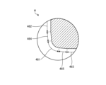
- FIG. 9 is a schematic enlarged view of the H section shown in FIG.
- the stepped portion 46 has a curved corner portion 461 in cross-sectional views shown in FIGS. Since the corner 461 of the stepped portion 46 is curved in this way, it is possible to facilitate the formation of air flow along the stepped portion 46 compared to the case where the corner 461 is at right angles, for example. . In other words, the airflow is less likely to be disturbed compared to when the corners 461 are at right angles. Therefore, the wind speed on the second opening 102 side can be further increased, and the heat radiation efficiency of the plurality of optical elements 3 can be further increased.
- the stepped portion 46 also has a vertical surface 462 , a horizontal surface 463 , a first inclined surface 464 and a second inclined surface 465 .
- the vertical surface 462 is a surface extending vertically toward the substrate 2 from the first region 201 side surface of the surface 411 facing the substrate 2 of the plate-like portion 41 .
- the horizontal plane 463 is a plane extending parallel to the substrate 2 toward the second opening 102 .
- the first inclined surface 464 is a surface that connects the corner portion 461 and the vertical surface 462 , and is a surface that is inclined away from the first opening 101 toward the corner portion 461 from the vertical surface 462 .
- the second inclined surface 465 is a surface that connects the corner portion 461 and the horizontal surface 463 , and is a surface that is inclined so as to approach the substrate 2 from the corner portion 461 toward the horizontal surface 463 .
- the air flow along the stepped portion 46 is further formed. can be made easier. Therefore, the wind speed on the second opening 102 side can be further increased, and the heat dissipation efficiency of the plurality of optical elements 3 can be further increased.
- FIG. 10 is a perspective view of the heat dissipating member 4 according to the first modified example as viewed obliquely from below.
- the plate-like portion 41 of the heat radiating member 4 may have a slope portion 47 instead of the stepped portion 46 .
- the slope portion 47 is an inclined surface that is inclined so as to approach the one main surface 21 of the substrate 2 toward the second opening 102 .
- FIG. 11 is a perspective view of the heat radiating member 4 according to the second modified example as viewed obliquely from below.
- FIG. 12 is a diagram of the semiconductor module 1 according to the second modified example viewed from the negative side of the X-axis.
- the first leg 42 of the heat radiating member 4 has a width from the first opening 101 to the second opening 102 in the direction perpendicular to the longitudinal direction of the first leg 42, that is, in the Y-axis direction. You may have the shape which spreads as it goes. With such a configuration, the width W2 of the first leg portion 42 on the second opening 102 side is larger than the width W1 of the first leg portion 42 on the first opening 101 side. Accordingly, the width W4 of the second opening 102 in the direction perpendicular to the longitudinal direction of the first leg 42, that is, the Y-axis direction, is smaller than the width W3 of the first opening 101 in the same direction. That is, the opening area of the second opening 102 is smaller than the opening area of the first opening 101 .
- the plate-like portion 41 according to the second modification may have the step portion 46 or the slope portion 47 described above.
- the semiconductor module 1 has the substrate 2, at least one semiconductor element positioned on the substrate, such as the optical element 3, and the heat dissipation member 4 in contact with the semiconductor element.
- the semiconductor module according to the embodiment when the substrate is viewed from above, the position of the semiconductor element is shifted from the center C0 of the substrate.
- the semiconductor module according to the embodiment it is possible to improve the heat dissipation efficiency of the semiconductor element.
- the width (length in the Y direction) of the first leg 42 and the second leg 43 is constant along the thickness direction (Z-axis direction),
- the shape of the two legs 43 is not limited to this.
- the width of the first leg 42 may decrease as it approaches the substrate 2 .
Landscapes
- Physics & Mathematics (AREA)
- General Physics & Mathematics (AREA)
- Optics & Photonics (AREA)
- Cooling Or The Like Of Semiconductors Or Solid State Devices (AREA)
Priority Applications (4)
| Application Number | Priority Date | Filing Date | Title |
|---|---|---|---|
| CN202380018981.XA CN118633154A (zh) | 2022-01-31 | 2023-01-31 | 半导体模块 |
| JP2023577087A JP7791217B2 (ja) | 2022-01-31 | 2023-01-31 | 半導体モジュール |
| EP23747174.3A EP4475180A1 (en) | 2022-01-31 | 2023-01-31 | Semiconductor module |
| US18/729,091 US20250164719A1 (en) | 2022-01-31 | 2023-01-31 | Semiconductor module |
Applications Claiming Priority (2)
| Application Number | Priority Date | Filing Date | Title |
|---|---|---|---|
| JP2022-013589 | 2022-01-31 | ||
| JP2022013589 | 2022-01-31 |
Publications (1)
| Publication Number | Publication Date |
|---|---|
| WO2023145964A1 true WO2023145964A1 (ja) | 2023-08-03 |
Family
ID=87471787
Family Applications (1)
| Application Number | Title | Priority Date | Filing Date |
|---|---|---|---|
| PCT/JP2023/003039 Ceased WO2023145964A1 (ja) | 2022-01-31 | 2023-01-31 | 半導体モジュール |
Country Status (5)
| Country | Link |
|---|---|
| US (1) | US20250164719A1 (https=) |
| EP (1) | EP4475180A1 (https=) |
| JP (1) | JP7791217B2 (https=) |
| CN (1) | CN118633154A (https=) |
| WO (1) | WO2023145964A1 (https=) |
Citations (4)
| Publication number | Priority date | Publication date | Assignee | Title |
|---|---|---|---|---|
| JP2000040834A (ja) | 1998-07-24 | 2000-02-08 | Mitsubishi Electric Corp | マルチチップモジュールの製造方法 |
| JP2003124663A (ja) * | 2001-10-09 | 2003-04-25 | Fujitsu Ltd | 冷却装置 |
| JP2010141279A (ja) * | 2008-11-14 | 2010-06-24 | Calsonic Kansei Corp | 素子の放熱構造及び方法 |
| WO2015045648A1 (ja) * | 2013-09-30 | 2015-04-02 | 富士電機株式会社 | 半導体装置、半導体装置の組み立て方法、半導体装置用部品及び単位モジュール |
Family Cites Families (5)
| Publication number | Priority date | Publication date | Assignee | Title |
|---|---|---|---|---|
| JP2001111158A (ja) | 1999-10-13 | 2001-04-20 | Sumitomo Electric Ind Ltd | 光通信モジュールおよびその製造方法 |
| JP2003264388A (ja) | 2002-03-08 | 2003-09-19 | Toshiba Kyaria Kk | 電気部品装置 |
| JP5075139B2 (ja) | 2009-01-30 | 2012-11-14 | 古河電気工業株式会社 | 並列光伝送装置 |
| JP5751261B2 (ja) | 2013-01-17 | 2015-07-22 | ヤマハ株式会社 | 熱電発電ユニット |
| JP5904146B2 (ja) | 2013-03-13 | 2016-04-13 | 日立金属株式会社 | 通信モジュール及びそれを備えた信号伝送装置 |
-
2023
- 2023-01-31 EP EP23747174.3A patent/EP4475180A1/en not_active Withdrawn
- 2023-01-31 US US18/729,091 patent/US20250164719A1/en active Pending
- 2023-01-31 CN CN202380018981.XA patent/CN118633154A/zh active Pending
- 2023-01-31 WO PCT/JP2023/003039 patent/WO2023145964A1/ja not_active Ceased
- 2023-01-31 JP JP2023577087A patent/JP7791217B2/ja active Active
Patent Citations (4)
| Publication number | Priority date | Publication date | Assignee | Title |
|---|---|---|---|---|
| JP2000040834A (ja) | 1998-07-24 | 2000-02-08 | Mitsubishi Electric Corp | マルチチップモジュールの製造方法 |
| JP2003124663A (ja) * | 2001-10-09 | 2003-04-25 | Fujitsu Ltd | 冷却装置 |
| JP2010141279A (ja) * | 2008-11-14 | 2010-06-24 | Calsonic Kansei Corp | 素子の放熱構造及び方法 |
| WO2015045648A1 (ja) * | 2013-09-30 | 2015-04-02 | 富士電機株式会社 | 半導体装置、半導体装置の組み立て方法、半導体装置用部品及び単位モジュール |
Also Published As
| Publication number | Publication date |
|---|---|
| JP7791217B2 (ja) | 2025-12-23 |
| EP4475180A1 (en) | 2024-12-11 |
| JPWO2023145964A1 (https=) | 2023-08-03 |
| CN118633154A (zh) | 2024-09-10 |
| US20250164719A1 (en) | 2025-05-22 |
Similar Documents
| Publication | Publication Date | Title |
|---|---|---|
| US6967845B2 (en) | Integrated heat dissipating device with curved fins | |
| JP3852253B2 (ja) | 電子部品の冷却装置及び電子機器 | |
| JP7339075B2 (ja) | 電気機器、電子制御装置 | |
| JP7549469B2 (ja) | 電子制御装置 | |
| CN103262675B (zh) | 能散失热负荷的机顶盒 | |
| US7967059B2 (en) | Heat dissipation device | |
| JP2901835B2 (ja) | 半導体装置 | |
| JP2005064384A (ja) | インターフェイスモジュール付lsiパッケージ及びそれに用いるヒートシンク | |
| CN102045989A (zh) | 热管散热模组 | |
| JP7397991B2 (ja) | 電子制御装置 | |
| CN111596514A (zh) | 一种激光光源及激光投影设备 | |
| WO2023100480A1 (ja) | 電子制御装置 | |
| JP3840970B2 (ja) | ヒートシンク | |
| WO2023145964A1 (ja) | 半導体モジュール | |
| JP2002185173A (ja) | 電子モジュール及びその実装装置 | |
| TW202420929A (zh) | 組合式散熱器結構 | |
| JP7454048B2 (ja) | 電子制御装置 | |
| KR101996616B1 (ko) | 방열 장치를 구비하는 전자기기 | |
| JP2011171686A (ja) | 放熱部付き金属ベースプリント基板 | |
| KR102034166B1 (ko) | 방열 장치를 구비하는 전자기기 | |
| JP3104491U (ja) | 放熱板を備えた配線基板および該配線基板を実装した電子機器 | |
| TWM619527U (zh) | 散熱組件及電子組件 | |
| WO2024071110A1 (ja) | 半導体モジュール | |
| JPS6271300A (ja) | 電子装置の放熱構造 | |
| JPH03208398A (ja) | 半導体装置 |
Legal Events
| Date | Code | Title | Description |
|---|---|---|---|
| 121 | Ep: the epo has been informed by wipo that ep was designated in this application |
Ref document number: 23747174 Country of ref document: EP Kind code of ref document: A1 |
|
| WWE | Wipo information: entry into national phase |
Ref document number: 18729091 Country of ref document: US |
|
| ENP | Entry into the national phase |
Ref document number: 2023577087 Country of ref document: JP Kind code of ref document: A |
|
| WWE | Wipo information: entry into national phase |
Ref document number: 202380018981.X Country of ref document: CN |
|
| WWE | Wipo information: entry into national phase |
Ref document number: 2023747174 Country of ref document: EP |
|
| NENP | Non-entry into the national phase |
Ref country code: DE |
|
| ENP | Entry into the national phase |
Ref document number: 2023747174 Country of ref document: EP Effective date: 20240902 |
|
| WWP | Wipo information: published in national office |
Ref document number: 18729091 Country of ref document: US |
|
| WWW | Wipo information: withdrawn in national office |
Ref document number: 2023747174 Country of ref document: EP |