WO2023145839A1 - 吸着基板 - Google Patents
吸着基板 Download PDFInfo
- Publication number
- WO2023145839A1 WO2023145839A1 PCT/JP2023/002509 JP2023002509W WO2023145839A1 WO 2023145839 A1 WO2023145839 A1 WO 2023145839A1 JP 2023002509 W JP2023002509 W JP 2023002509W WO 2023145839 A1 WO2023145839 A1 WO 2023145839A1
- Authority
- WO
- WIPO (PCT)
- Prior art keywords
- conductive layer
- end surface
- adsorption substrate
- substrate
- projecting portion
- Prior art date
- Legal status (The legal status is an assumption and is not a legal conclusion. Google has not performed a legal analysis and makes no representation as to the accuracy of the status listed.)
- Ceased
Links
Images


Classifications
-
- H—ELECTRICITY
- H02—GENERATION; CONVERSION OR DISTRIBUTION OF ELECTRIC POWER
- H02N—ELECTRIC MACHINES NOT OTHERWISE PROVIDED FOR
- H02N13/00—Clutches or holding devices using electrostatic attraction, e.g. using Johnson-Rahbek effect
-
- H—ELECTRICITY
- H10—SEMICONDUCTOR DEVICES; ELECTRIC SOLID-STATE DEVICES NOT OTHERWISE PROVIDED FOR
- H10P—GENERIC PROCESSES OR APPARATUS FOR THE MANUFACTURE OR TREATMENT OF DEVICES COVERED BY CLASS H10
- H10P72/00—Handling or holding of wafers, substrates or devices during manufacture or treatment thereof
- H10P72/70—Handling or holding of wafers, substrates or devices during manufacture or treatment thereof for supporting or gripping
Definitions
- the disclosed embodiments relate to adsorption substrates.
- An electrostatic chuck that holds an object to be processed such as a semiconductor wafer is known.
- Such an electrostatic chuck includes an adsorption substrate in which an electrode is positioned inside an insulating substrate (see Patent Documents 1 and 2, for example).
- JP 2015-162481 A Japanese Patent Application Laid-Open No. 2020-25101
- An adsorption substrate includes an insulating base, a conductive layer, and a projecting portion.
- the substrate has a first surface for holding an object to be processed and a second surface opposite to the first surface.
- a conductive layer is positioned within the substrate and extends along the first surface.
- the protruding portion is located inside the base and protrudes from the conductive layer toward the second surface.
- the protruding portion has a first end surface in contact with the conductive layer and a second end surface located on the second surface side. A first distance between the first end surface and the second end surface is greater than half the thickness of the conductive layer.
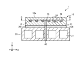
- FIG. 1 is a cross-sectional view showing an example of an electrostatic chuck having an attraction substrate according to the first embodiment.
- FIG. 2 is an enlarged view of area A shown in FIG.
- FIG. 3 is a cross-sectional view taken along line BB shown in FIG.
- FIG. 4A is a cross-sectional view showing another example of a protrusion included in the adsorption substrate according to the first embodiment;
- FIG. 4B is a cross-sectional view showing another example of a protrusion included in the adsorption substrate according to the first embodiment;
- 5A is a cross-sectional view showing another example of the adsorption substrate according to the first embodiment;
- FIG. 5B is a cross-sectional view showing another example of the adsorption substrate according to the first embodiment;
- FIG. 5A is a cross-sectional view showing another example of the adsorption substrate according to the first embodiment;
- FIG. 5B is a cross-sectional view showing another example of the adsorption
- FIG. 5C is a cross-sectional view showing another example of the adsorption substrate according to the first embodiment
- FIG. 6 is a cross-sectional view showing another example of the electrostatic chuck according to the first embodiment
- FIG. 7 is a cross-sectional view showing an example of an electrostatic chuck having an attraction substrate according to the second embodiment.
- FIG. 8 is an enlarged view of area C shown in FIG.
- FIG. 1 is a cross-sectional view showing an example of an electrostatic chuck having an attraction substrate according to the first embodiment.
- FIG. 2 is an enlarged view of area A shown in FIG.
- FIG. 3 is a cross-sectional view taken along line BB shown in FIG.
- the electrostatic chuck 1 includes an adsorption substrate 10 , a heat exchanger 20 and a bonding material 30 .
- the electrostatic chuck 1 uses electrostatic force generated on the surface of the attraction substrate 10 to attract an object to be processed such as a semiconductor wafer.
- the adsorption substrate 10 has, for example, a substantially disk shape.
- the adsorption substrate 10 may be disc-shaped, for example, with a diameter of 50 mm to 400 mm and a thickness of 2 mm to 20 mm.
- the adsorption substrate 10 has a first surface 10a and a second surface 10b facing each other in the thickness direction.
- the first surface 10a is a holding surface that holds an object to be processed.
- the second surface 10b is located on the opposite side of the first surface 10a and may be bonded to the heat exchanger 20 using a bonding material 30.
- the adsorption substrate 10 has a base 11 , a conductive layer 12 , protrusions 13 and conductors 14 .
- the base 11 has insulating properties.
- the substrate 11 contains, for example, ceramics such as aluminum oxide (Al 2 O 3 ), aluminum nitride (AlN), yttria (Y 2 O 3 ), etc. as a main component.
- the conductive layer 12 is located inside the base 11 .
- the conductive layer 12 extends along the first surface 10a in the vicinity of the first surface 10a.
- the conductive layer 12 has, for example, a substantially circular shape in a plan view.
- the conductive layer 12 can have a diameter of 30 mm to 398 mm in plan view, for example.
- the conductive layer 12 has a thickness t1.
- Conductive layer 12 contains noble metal (for example, platinum (Pt), palladium (Pd), etc.) as a main component.
- the present disclosure exemplifies the case of a unipolar structure having one conductive layer 12, the number of conductive layers 12 is not limited to one, and a bipolar structure having two conductive layers 12 may be used. .
- the projecting portion 13 is positioned inside the base 11 .
- the protruding portion 13 is positioned to protrude from the conductive layer 12 toward the second surface 10b.
- the projecting portion 13 has a first end surface 131 in contact with the conductive layer 12 and a second end surface 132 located on the second surface 10b side.
- a plurality of projecting portions 13 having a substantially circular columnar shape in plan view may be connected to the conductive layer 12 .
- the shape of the projecting portion 13 in plan view is not limited to that shown in FIG. 3, and may be, for example, an elliptical shape or a polygonal shape.
- the projecting portion 13 is positioned so as to fit into the concave base 11, the projecting portion 13 is unlikely to come off from the base 11 even when the attraction substrate 10 receives an external force, for example. As a result, the conductive layer 12 connected to the projecting portion 13 is less likely to come off from the base 11 . Therefore, according to the adsorption substrate 10 according to the present embodiment, delamination is less likely to occur.
- the projecting portion 13 has a first distance d1 between the first end surface 131 and the second end surface 132. As shown in FIG. This first distance d1 is larger than half the thickness t1 of the conductive layer 12 . Also, the first distance d1 may be greater than the second distance d2 between the first surface 10a and the conductive layer 12 . In this way, the attraction substrate 10 has the protruding portions 13 whose shape is different from the fine irregularities located on the surface of the conductive layer 12, so that the occurrence of delamination can be further reduced.
- the thickness t1 may be in the range of 2 ⁇ m to 20 ⁇ m, for example.
- the first distance d1 may be 1 ⁇ m to 3000 ⁇ m.
- the first distance d1 may be 500 ⁇ m or more.
- the second distance d2 can be set to 300 ⁇ m, for example.
- the material of the protrusion 13 may be the same as that of the conductive layer 12, for example. Accordingly, the adsorption substrate 10 can be manufactured without separately preparing a material for the projecting portion 13 .
- the material of the projecting portion 13 may be different from that of the conductive layer 12 .
- the conductor 14 is connected to a power supply terminal 40 drawn outside, and power is supplied to the conductive layer 12 via the conductor 14 . Therefore, the projecting portion 13 may have insulating properties.
- the projecting portion 13 may be made of, for example, a metal material, a carbon material, or a thermosetting resin.
- the projecting portion 13 may be made of a ceramic different from that of the base 11 .
- a heater an RF (radio frequency) electrode, and the like, for example, may be arranged inside the base 11 .
- the heat exchanger 20 receives heat from the adsorption substrate 10 and dissipates it to the outside.
- the heat exchanger 20 is bonded to the second surface 10b of the adsorption substrate 10 with a bonding material 30 such as silicone.
- the heat exchanger 20 may have a channel 21 through which a cooling medium flows.
- the heat exchanger 20 according to the embodiment may be made of metal such as aluminum, or may be made of ceramic such as alumina or silicon carbide.
- the heat exchanger 20 may be used as the RF electrode of the adsorption substrate 10.
- the heat exchanger 20 is made of ceramic, a metal layer may be formed on the outer surface of the heat exchanger 20 and the metal layer may be used as the RF electrode of the electrostatic chuck 1 .
- the adsorption substrate 10 has a protruding portion 13 with a constant cross-sectional shape in the thickness direction, but it is not limited to this.
- 4A and 4B are cross-sectional views showing other examples of protrusions of the adsorption substrate according to the first embodiment.
- the adsorption substrate 10 may have a tapered protruding portion 13 whose cross-sectional shape changes so that the cross-sectional area increases from the first end surface 131 toward the second end surface 132 .
- the contact area between the projecting portion 13 and the substrate 11 increases even when the adsorption substrate 10 receives an external force. It becomes difficult for the conductive layer 12 connected to the base 11 to come off from the base 11 .
- the adsorption substrate 10 according to the present embodiment it is possible to further reduce the occurrence of delamination.
- the projecting portion 13 has a third distance d3, which is the distance between the first end surface 131 and the second end surface 132.
- Such third distance d3 may be, for example, 1 ⁇ m or more.
- the third distance d3 can be in the range of 0.5 mm to 3.0 mm, for example.
- the diameter D1 of the first end surface 131 can be set to, for example, 0.3 mm to 2.5 mm.
- a diameter D2 of the second end surface 132 can be, for example, 0.5 mm to 3.0 mm.
- the thickness t2 of the conductive layer 12 can be in the range of 5 ⁇ m to 20 ⁇ m, for example.
- the attraction substrate 10 may have a tapered projecting portion 13 whose cross-sectional shape changes so that the cross-sectional area decreases from the first end surface 131 toward the second end surface 132. .
- the contact area between the projecting portion 13 and the substrate 11 increases even when the adsorption substrate 10 receives an external force. It becomes difficult for the conductive layer 12 connected to the base 11 to come off from the base 11 .
- the adsorption substrate 10 according to the present embodiment it is possible to further reduce the occurrence of delamination.
- the projecting portion 13 has a fourth distance d4, which is the distance between the first end surface 131 and the second end surface 132.
- the fourth distance d4 may be 1 ⁇ m or more.
- it can be in the range of 0.5 mm to 3.0 mm.
- the diameter D3 of the first end surface 131 can be set to, for example, 0.5 mm to 3.0 mm.
- a diameter D4 of the second end surface 132 can be, for example, 0.3 mm to 2.5 mm.
- the adsorption substrate 10 according to the present embodiment shows an example in which the plurality of projecting portions 13 are evenly distributed, but it is not limited to this.
- 5A to 5C are cross-sectional views showing another example of the adsorption substrate according to the first embodiment.
- the adsorption substrate 10 may be positioned such that the protruding portions 13 positioned in the outer peripheral region 122 of the conductive layer 12 in plan view are denser than the inner peripheral region 121 .
- the inner peripheral region 121 can be, for example, a portion that satisfies the diameter L1 ⁇ 0.6 ⁇ L with respect to the diameter L of the conductive layer 12 in plan view.
- the outer peripheral region 122 is the remaining portion of the conductive layer 12 in plan view located outside the inner peripheral region 121 .
- the adsorption substrate 10 may have cylindrical projections 13 that are concentrically positioned in a plan view.
- the adsorption substrate 10 may have a projecting portion 13 inside the outline 12a of the conductive layer 12 in plan view.
- peeling from the contour 12a of the conductive layer 12 can be reduced.
- the distance between the contour 12a of the conductive layer 12 and the protruding portion 13 adjacent to the contour 12a can be, for example, 10 mm to 20 mm. If the attraction substrate has through holes through which lift pins for lifting the wafer pass, the conductive layer 12 is arranged so as to avoid the through holes.
- a contour 12a exists in the conductive layer around the through-hole, and the separation of the conductive layer 12 caused from the contour 12a is prevented by setting the distance between the contour 12a and the protrusion 13 adjacent to the contour 12a to be, for example, 10 mm to 20 mm. can be reduced. Also, the interval between adjacent protruding portions 13 can be set to 20 mm, for example. In addition, when the attraction substrate 10 has a plurality of conductive layers 12 , the arrangement of the projecting portions 13 can be determined for each of the plurality of conductive layers 12 .
- FIG. 6 is a cross-sectional view showing another example of the electrostatic chuck according to the first embodiment.
- a power supply terminal 40 inserted into the adsorption substrate 10 through an opening 15 provided in the adsorption substrate 10 supplies power to the conductive layer 12 through a connecting portion 16 such as a brazing material. It differs from the electrostatic chuck 1 shown in FIG. 1 in that power can be supplied.
- the mode of power supply to the conductive layer 12 shown in FIGS. 1 and 6 is merely an example, and is not limited to the illustrated one.
- FIG. 7 is a cross-sectional view showing an example of an electrostatic chuck having an attraction substrate according to the second embodiment.
- FIG. 8 is an enlarged view of area C shown in FIG.
- the attraction substrate 10 according to this embodiment differs from the attraction substrate 10 according to the first embodiment in that the projecting portion 13 has a flat portion 17 .
- the flat portion 17 is connected to the second end surface 132 of the protruding portion 13 and extends along the first surface 10 a of the adsorption substrate 10 .
- the projecting portion 13 having the flat portion 17 has a stepped shape in a cross-sectional view.
- the projecting portion 13 has a different area between the flat portion 17 and the portion located between the first end surface 131 and the second end surface 132 when viewed from the first surface 10a side.
- the projecting portion 13 has a third end surface 171 and a fourth end surface 172 .
- the third end face 171 is in contact with the second end face 132 .
- the fourth end face 172 is located apart from the third end face 171 .
- a flat portion 17 is a portion of the projecting portion 13 located between the third end surface 171 and the fourth end surface 172 .
- the projecting portion 13 Since the projecting portion 13 has the flat portion 17, even if the attraction substrate 10 receives an external force, the projecting portion 13 is more difficult to come off from the base 11, so that the conductive layer connected to the projecting portion 13 12 becomes difficult to peel off from the base 11. - ⁇ Thus, according to the adsorption substrate 10 according to the present embodiment, delamination is less likely to occur.
- the diameter D5 of the first end surface 131 can be set to 0.3 mm to 2.5 mm, for example.
- the diameter D6 of the fourth end surface 172 can be, for example, 0.5 mm to 3.0 mm.
- the diameter of the second end surface 132 may be the same as or different from the diameter D5 of the first end surface 131 .
- the diameter of the third end face 171 may be the same as or different from the diameter D6 of the fourth end face 172 .
- the area of the flat portion 17 when viewed from the first surface 10 a side may be larger than the area of the second end surface 132 . This further reduces delamination.
- the flat portion 17 may have a smaller area than the conductive layer 12 when viewed from the first surface 10a side. This makes it difficult for the projecting portion 13 to come off from the base 11 together with the flat portion 17 .
- the area of the projecting portion 13 when the portion from the first end surface 131 to the second end surface 132 is viewed from the first surface 10a side is 5% to 85% of the area of the flat portion 17 when viewed from the first surface 10a side. %, the occurrence of delamination can be further reduced.
- the area of the protruding portion 13 when the portion from the first end surface 131 to the second end surface 132 is viewed from the first surface 10a side is 5% to 30% of the area of the flat portion 17 when viewed from the first surface 10a side. %, delamination is even less likely to occur.
- the flat portion 17 has a thickness t3.
- the thickness t3 may be smaller than the first distance d1 between the first end surface 131 and the second end surface 132 of the protruding portion 13 .
- the thickness t3 of the flat portion 17 may be greater than the thickness t1 of the conductive layer 12 .
- the thickness t3 may be, for example, 1 ⁇ m or more.
- the thickness t3 may be in the range of 2 ⁇ m to 20 ⁇ m.
- the thickness t3 may be 0.5 ⁇ m to 3.0 ⁇ m.
- the thickness t3 of the flat portion 17 may be greater than the thickness t1 of the conductive layer 12 .
- the thickness t3 can be in the range of 2 to 100 times the thickness t1, for example.
- the material of the flat portion 17 may be, for example, the same as that of other portions of the projecting portion 13 . Also, the material of the flat portion 17 may be the same as that of the conductive layer 12 .
- the flat portion 17 may be located on each of the protruding portions 13 protruding from the conductive layer 12, or may be provided only on some of them. Moreover, the flat portion 17 may be positioned so as to straddle two or more protruding portions 13 .
- the shape of the projecting portion 13 having the flat portion 17 is not limited to that shown in FIG.
- the diameter of the first end face 131 may be formed to be larger than the diameter of the fourth end face 172 .
- a portion of the protruding portion 13 located on the conductive layer 12 side between the first end surface 131 and the second end surface 132 has a columnar shape extending in a first direction along the XY plane (for example, the Y-axis direction).
- the flat portion 17 may have a columnar shape extending in a second direction (for example, the X-axis direction) that intersects the first direction, so that the projecting portion 13 may be substantially X-shaped in plan view.
- the protrusion 13 has the flat portion 17, the cross-sectional shape of the protrusion 13 changes in the thickness direction (Z-axis direction). This increases the surface area of the projecting portion 13 . Therefore, the contact area between the projecting portion 13 and the base 11 is increased, and the conductive layer 12 connected to the projecting portion 13 is less likely to come off from the base 11 . Thus, according to the adsorption substrate 10 shown in FIG. 8, the occurrence of delamination can be further reduced.
- the adsorption substrate 10 can be produced, for example, as follows.
- the adsorption substrate 10 includes the insulating substrate 11, the conductive layer 12, and the projecting portion 13.
- the substrate 11 has a first surface 10a for holding an object to be processed and a second surface 10b opposite to the first surface.
- the conductive layer 12 is located inside the base 11 and extends along the first surface 10a.
- the protrusion 13 is located inside the base 11 and protrudes from the conductive layer 12 toward the second surface 10b.
- the projecting portion 13 has a first end surface 131 in contact with the conductive layer 12 and a second end surface 132 located on the second surface 10b side.
- a first distance d1 between the first end surface 131 and the second end surface 132 is larger than half the thickness t1 of the conductive layer 12 . This makes delamination less likely to exist.
Landscapes
- Container, Conveyance, Adherence, Positioning, Of Wafer (AREA)
Priority Applications (1)
| Application Number | Priority Date | Filing Date | Title |
|---|---|---|---|
| JP2023576991A JP7844511B2 (ja) | 2022-01-28 | 2023-01-26 | 吸着基板 |
Applications Claiming Priority (2)
| Application Number | Priority Date | Filing Date | Title |
|---|---|---|---|
| JP2022012408 | 2022-01-28 | ||
| JP2022-012408 | 2022-01-28 |
Publications (1)
| Publication Number | Publication Date |
|---|---|
| WO2023145839A1 true WO2023145839A1 (ja) | 2023-08-03 |
Family
ID=87471566
Family Applications (1)
| Application Number | Title | Priority Date | Filing Date |
|---|---|---|---|
| PCT/JP2023/002509 Ceased WO2023145839A1 (ja) | 2022-01-28 | 2023-01-26 | 吸着基板 |
Country Status (2)
| Country | Link |
|---|---|
| JP (1) | JP7844511B2 (https=) |
| WO (1) | WO2023145839A1 (https=) |
Citations (2)
| Publication number | Priority date | Publication date | Assignee | Title |
|---|---|---|---|---|
| JP2004259805A (ja) * | 2003-02-25 | 2004-09-16 | Kyocera Corp | 静電チャック |
| JP2013084938A (ja) * | 2011-09-30 | 2013-05-09 | Toto Ltd | 静電チャック |
-
2023
- 2023-01-26 JP JP2023576991A patent/JP7844511B2/ja active Active
- 2023-01-26 WO PCT/JP2023/002509 patent/WO2023145839A1/ja not_active Ceased
Patent Citations (2)
| Publication number | Priority date | Publication date | Assignee | Title |
|---|---|---|---|---|
| JP2004259805A (ja) * | 2003-02-25 | 2004-09-16 | Kyocera Corp | 静電チャック |
| JP2013084938A (ja) * | 2011-09-30 | 2013-05-09 | Toto Ltd | 静電チャック |
Also Published As
| Publication number | Publication date |
|---|---|
| JP7844511B2 (ja) | 2026-04-13 |
| JPWO2023145839A1 (https=) | 2023-08-03 |
Similar Documents
| Publication | Publication Date | Title |
|---|---|---|
| CN108470702B (zh) | 静电吸盘 | |
| KR101994006B1 (ko) | 정전 척 | |
| CN104952779B (zh) | 静电吸盘 | |
| JP6587223B1 (ja) | 静電チャック | |
| JP7430489B2 (ja) | 静電チャック、静電チャック装置 | |
| JP6971183B2 (ja) | 基板固定装置 | |
| WO2023145839A1 (ja) | 吸着基板 | |
| JP3767719B2 (ja) | 静電吸着装置 | |
| JP6449802B2 (ja) | 半導体製造用部品 | |
| JP6901547B2 (ja) | 半導体製造用部品 | |
| JP2025066175A (ja) | 保持装置 | |
| CN114026681A (zh) | 晶片载置台 | |
| KR102203859B1 (ko) | 절연 저항이 우수한 정전척 | |
| JP2003179129A (ja) | 静電チャック装置 | |
| JP2025084481A (ja) | 静電チャック | |
| WO2024058183A1 (ja) | 吸着基板 | |
| JP2023177720A (ja) | 保持装置 | |
| JP7373111B2 (ja) | 静電チャック | |
| JP2020004809A (ja) | 保持装置 | |
| JP7714063B1 (ja) | 保持装置 | |
| US20230178408A1 (en) | Electrostatic chuck | |
| JP2025037120A (ja) | 保持部材 | |
| JP2025112084A (ja) | 保持装置 | |
| CN121772679A (zh) | 静电吸盘 | |
| KR20250139193A (ko) | 정전 척 부재 및 정전 척 장치 |
Legal Events
| Date | Code | Title | Description |
|---|---|---|---|
| 121 | Ep: the epo has been informed by wipo that ep was designated in this application |
Ref document number: 23747049 Country of ref document: EP Kind code of ref document: A1 |
|
| ENP | Entry into the national phase |
Ref document number: 2023576991 Country of ref document: JP Kind code of ref document: A |
|
| NENP | Non-entry into the national phase |
Ref country code: DE |
|
| 122 | Ep: pct application non-entry in european phase |
Ref document number: 23747049 Country of ref document: EP Kind code of ref document: A1 |