WO2023090223A1 - 電流センサ - Google Patents
電流センサ Download PDFInfo
- Publication number
- WO2023090223A1 WO2023090223A1 PCT/JP2022/041774 JP2022041774W WO2023090223A1 WO 2023090223 A1 WO2023090223 A1 WO 2023090223A1 JP 2022041774 W JP2022041774 W JP 2022041774W WO 2023090223 A1 WO2023090223 A1 WO 2023090223A1
- Authority
- WO
- WIPO (PCT)
- Prior art keywords
- core
- gap
- width direction
- bus bar
- line segment
- Prior art date
Links
Images


Classifications
-
- G—PHYSICS
- G01—MEASURING; TESTING
- G01R—MEASURING ELECTRIC VARIABLES; MEASURING MAGNETIC VARIABLES
- G01R15/00—Details of measuring arrangements of the types provided for in groups G01R17/00 - G01R29/00, G01R33/00 - G01R33/26 or G01R35/00
- G01R15/14—Adaptations providing voltage or current isolation, e.g. for high-voltage or high-current networks
- G01R15/20—Adaptations providing voltage or current isolation, e.g. for high-voltage or high-current networks using galvano-magnetic devices, e.g. Hall-effect devices, i.e. measuring a magnetic field via the interaction between a current and a magnetic field, e.g. magneto resistive or Hall effect devices
Definitions
- the present disclosure relates to current sensors.
- a current sensor that detects AC current flowing through an inverter for driving an AC motor for a hybrid vehicle or an electric vehicle.
- This current sensor includes a bus bar through which an alternating current of an inverter flows, a core through which a magnetic field generated by the alternating current flowing through the bus bar passes, and a sensor chip arranged in a gap formed in the core. The sensor chip detects the magnetic field passing through the core gap, and the current sensor detects alternating current flowing through the inverter.
- An object of the present disclosure is to provide a current sensor that suppresses magnetic saturation.
- a current sensor includes a bus bar formed in a plate shape, a core hole into which the bus bar is inserted, a first end surface facing the width direction of the bus bar, a first a second end surface facing the end surface in the width direction; a gap forming portion formed by the first end surface and the second end surface and including a gap communicating with the core hole and the outside; and a gap forming portion connected to the gap forming portion. and a core bottom portion connected to the core lateral portion and extending in the width direction and forming a core hole with the gap forming portion and the core lateral portion.
- a detection unit that is arranged in the gap and detects the strength of the magnetic field generated in the gap by the current flowing through the bus bar, the magnetic permeability of the lateral portion of the core being higher than the magnetic permeability of the bottom portion of the core. It is the current sensor that is getting bigger.
- the linear region of the magnetic flux density in the core lateral portion with respect to the magnetic field strength becomes larger than the linear region of the magnetic flux density in the core bottom portion with respect to the magnetic field strength, so magnetic saturation in the core lateral portion is suppressed. Therefore, magnetic saturation of the core is suppressed.
- the current sensor includes a bus bar formed in a plate shape, a core hole into which the bus bar is inserted, a first end surface facing the width direction of the bus bar, a gap forming portion including a second end face facing the first end face in the width direction and a gap formed by the first end face and the second end face and communicating with the core hole and the outside; and a gap forming portion a core bottom portion connected to the bus bar and extending in the thickness direction of the busbar; and a core bottom portion connected to the core lateral portion and extending in the width direction and forming a core hole with the gap forming portion and the core lateral portion.
- a detector disposed in the gap and detecting the strength of the magnetic field generated in the gap by the current flowing through the busbar, wherein the magnetic permeability of the lateral portion of the core is equal to the magnetic permeability of the bottom portion of the core.
- the linear region of the magnetic flux density at the bottom of the core with respect to the strength of the magnetic field becomes larger than the linear region of the magnetic flux density at the lateral portion of the core with respect to the strength of the magnetic field, so magnetic saturation at the bottom of the core is suppressed. Therefore, magnetic saturation of the core is suppressed.
- the current sensor includes a bus bar formed in a plate shape, a core hole into which the bus bar is inserted, a first end surface facing the width direction of the bus bar, a gap forming portion including a second end face facing the first end face in the width direction and a gap formed by the first end face and the second end face and communicating with the core hole and the outside; and a gap forming portion a core bottom portion connected to the bus bar and extending in the thickness direction of the busbar; and a core bottom portion connected to the core lateral portion and extending in the width direction and forming a core hole with the gap forming portion and the core lateral portion.
- a detector arranged in the gap and detecting the strength of the magnetic field generated in the gap by the current flowing in the bus bar, wherein the length of the bottom of the core in the thickness direction and the width of the core in the width direction It is a current sensor in which the length of the core is the same and the magnetic permeability of the core lateral part and the magnetic permeability of the core bottom are different.
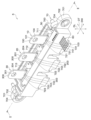
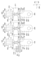
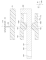
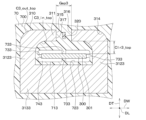
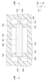
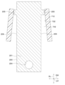
- FIG. 1 is a perspective view of a current sensor according to a first embodiment
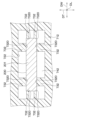
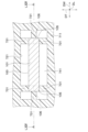
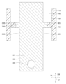
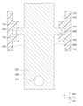
- FIG. 2 is a top view of busbars, cores, detectors, lead wires, substrates, and terminals of the current sensor
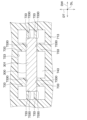
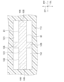
- FIG. 4 is a diagram showing the relationship between the strength of the magnetic field, the magnetic flux density applied to the first easy axis portion, and the magnetic flux density applied to the first hard axis portion; Sectional drawing of the current sensor of 2nd Embodiment. Sectional drawing of the current sensor of 3rd Embodiment.
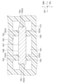
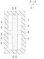
- FIG. 2 is a top view of busbars, cores, detectors, lead wires, substrates, and terminals of the current sensor; Sectional drawing of the current sensor of 4th Embodiment.
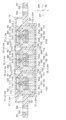
- FIG. 21 is a cross-sectional view of the first core and the first detector of the current sensor of the fourteenth embodiment; Sectional drawing of the 2nd core of a current sensor, and a 2nd detection part. Sectional drawing of the 3rd core of an electric current sensor, and a 3rd detection part.
- FIG. 21 is a cross-sectional view of the first core and the first detector of the current sensor of the fourteenth embodiment; Sectional drawing of the 2nd core of a current sensor, and a 2nd detection part. Sectional drawing of the 3rd core of an electric current sensor, and a 3rd detection part.
- FIG. 21 is a cross-sectional view of the first core of the current sensor of the fifteenth embodiment; Sectional drawing of the 2nd core of a current sensor.
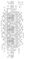
- FIG. 21 is a cross-sectional view of the first core, the second core and the third core in the current sensor of the seventeenth embodiment;
- FIG. 21 is a cross-sectional view of the first core, the second core and the third core in the current sensor of the eighteenth embodiment;
- FIG. 21 is a cross-sectional view of the first core, the second core and the third core in the current sensor of the eighteenth embodiment;
- FIG. 20 is a cross-sectional view of the first core, the second core, and the third core in the current sensor of the nineteenth embodiment; Sectional drawing of the 1st core, the 2nd core, and the 3rd core in the current sensor of 20th Embodiment.
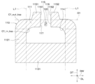
- FIG. 21 is a cross-sectional view of the first plate portion of the first bus bar and the first opening of the case in the current sensor of the twenty-first embodiment; XXXVI-XXXVI line sectional view of FIG. XXXVII-XXXVII line sectional view of FIG. Sectional drawing of the 2nd board part of the 2nd bus bar in a current sensor, and the 2nd opening part of a case. XXXIX-XXIX line sectional view of FIG.
- FIG. 12 is a cross-sectional view of the first plate portion of the first busbar and the first opening of the case in the current sensor of the twenty-second embodiment; Sectional drawing of the 2nd board part of the 2nd bus bar in a current sensor, and the 2nd opening part of a case. Sectional drawing of the 3rd board
- FIG. 12 is a cross-sectional view of the first plate portion of the first bus bar and the first opening of the case in the current sensor of the twenty-third embodiment; Sectional drawing of the 2nd board part of the 2nd bus bar in a current sensor, and the 2nd opening part of a case. Sectional drawing of the 3rd board
- FIG. 21 is a cross-sectional view of the first plate portion of the first bus bar and the first opening of the case in the current sensor of the twenty-fourth embodiment; Sectional drawing of the 2nd board part of the 2nd bus bar in a current sensor, and the 2nd opening part of a case.
- FIG. 21 is a cross-sectional view of the first plate portion of the first bus bar and the first opening of the case in the current sensor of the twenty-fifth embodiment; Sectional drawing of the 2nd board part of the 2nd bus bar in a current sensor, and the 2nd opening part of a case. Sectional drawing of the 3rd board
- FIG. 21 is a cross-sectional view of the first plate portion of the first bus bar and the first opening of the case in the current sensor of the twenty-fifth embodiment; Sectional drawing of the 2nd board part of the 2nd bus bar in a current sensor, and the 2nd opening part of a case. Sectional drawing of the 3rd board
- FIG. 21 is a cross-sectional view of the first plate portion of the first bus bar and the first opening of the case in the
- FIG. 14 is a cross-sectional view of the first bus bar, first core, first detection section, and case in the current sensor of the twenty-sixth embodiment; Sectional drawing of the 2nd bus bar in a current sensor, a 2nd core, a 2nd detection part, and a case. Sectional drawing of the 3rd bus bar in a current sensor, a 3rd core, a 3rd detection part, and a case.
- FIG. 4 is a relationship diagram of a first ratio and an amplitude ratio in a current sensor; FIG.
- FIG. 21 is a cross-sectional view of a first bus bar, a first core, and a first detector in a current sensor according to a twenty-seventh embodiment; Sectional drawing of the 2nd bus bar in a current sensor, a 2nd core, and a 2nd detection part. Sectional drawing of the 3rd bus bar in a current sensor, a 3rd core, and a 3rd detection part.
- FIG. 20 is a cross-sectional view of the first bus bar and the first opening of the case in the current sensor of the twenty-eighth embodiment; LXIV-LXIV line sectional view of FIG. Sectional drawing of the 2nd bus bar in a current sensor, and the 2nd opening part of a case.
- LXVI-LXVI line sectional view of FIG. Sectional drawing of the 3rd bus bar in a current sensor, and the 3rd opening part of a case.
- LXVIII-LXVIII line sectional view of FIG. FIG. 20 is a cross-sectional view of the first bus bar and the first opening of the case in the current sensor of the twenty-ninth embodiment; Sectional drawing of the 2nd bus bar in a current sensor, and the 2nd opening part of a case. Sectional drawing of the 3rd bus bar in a current sensor, and the 3rd opening part of a case.
- FIG. 21 is a cross-sectional view of the first bus bar and the first opening of the case in the current sensor of the thirtieth embodiment; Sectional drawing of the 2nd bus bar in a current sensor, and the 2nd opening part of a case. Sectional drawing of the 3rd bus bar in a current sensor, and the 3rd opening part of a case.
- FIG. 21 is a cross-sectional view of the first bus bar and the first opening of the case in the current sensor of the thirty-first embodiment; Sectional drawing of the 2nd bus bar in a current sensor, and the 2nd opening part of a case. Sectional drawing of the 3rd bus bar in a current sensor, and the 3rd opening part of a case.
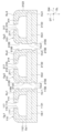
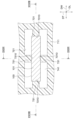
- the current sensor 5 of this embodiment is used in an inverter that drives a three-phase AC motor mounted on a vehicle (not shown).
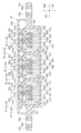
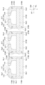
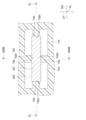
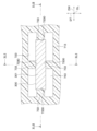
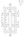
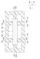
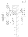
- the current sensor 5 includes a first sensor 10, a second sensor 20, a third sensor 30, a substrate 50, a plurality of terminals 60, and a case 70, as shown in FIGS.
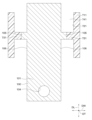
- the first sensor 10 has a first busbar 100 , a first core 110 , a first detection section 120 and a first lead wire 130 .
- the first bus bar 100 is made of copper or the like and formed into a plate shape. Moreover, the surface of the first bus bar 100 is plated to prevent the surface from being oxidized, if necessary. Further, first bus bar 100 has first plate portion 101 , first extension portion 102 and second extension portion 103 .
- the first plate portion 101 includes a first bolt hole 104 .
- a bolt (not shown) is inserted into the first bolt hole 104 and the hole provided in the inverter. Thereby, the first plate portion 101 is connected to a part of the inverter.
- the longitudinal direction DL of the first plate portion 101 is simply referred to as the longitudinal direction DL for convenience.
- the width direction DW of the first plate portion 101 is simply referred to as the width direction DW.
- the thickness direction DT of the first plate portion 101 is simply referred to as the thickness direction DT.
- the first extension portion 102 is connected to the side of the first plate portion 101 opposite to the first bolt hole 104 . Also, the first extension portion 102 extends in the thickness direction DT from the boundary portion between the first extension portion 102 and the first plate portion 101 .
- the second extension portion 103 is connected to the side of the first extension portion 102 opposite to the first plate portion 101 . Also, the second extension 103 extends in the longitudinal direction DL from the boundary between the second extension 103 and the first extension 102 . Furthermore, the second extension 103 is connected to part of the inverter by being welded to the part of the inverter.
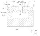
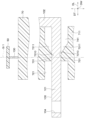
- the first core 110 is made of a soft magnetic material such as permalloy or a grain-oriented electrical steel sheet and is formed in a C shape.
- the first core 110 is formed by bending a plate-like soft magnetic material into a C shape.
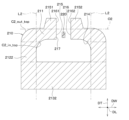
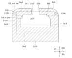
- First core 110 also includes first gap forming portion 111 , first easy shaft portion 112 , first hard shaft portion 113 and first core hole 114 .
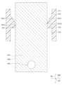
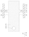
- the first gap forming portion 111 is formed in a plate shape extending in the width direction DW. Moreover, the first gap forming portion 111 is separated from the first bus bar 100 in the thickness direction DT. Further, a first lateral outer corner portion C1_out_top, which is a corner portion on the outer side in the width direction DW of the first gap forming portion 111, has an R shape. Also, the first gap forming portion 111 includes a first core end surface 115 , a second core end surface 116 and a first gap 117 . The first core end face 115 overlaps the projected second core end face 116 when the second core end face 116 is projected in the width direction DW. The first gap 117 is a space defined by the first core end face 115 and the second core end face 116 . Further, first gap 117 communicates with first core hole 114 and the outside of first core 110 .
- the surface of the first plate portion 101 facing the first core end surface 115 and the second core end surface 116 in the thickness direction DT is defined as a first plate surface S1.
- a portion of the first plate surface S1 overlapping the projected first core end surface 115 when the first core end surface 115 is projected onto the first plate surface S1 in the thickness direction DT is defined as a first projected portion Ps1.
- a portion of the first plate surface S1 overlapping the projected second core end surface 116 when the second core end surface 116 is projected onto the first plate surface S1 in the thickness direction DT is referred to as a second projected portion Ps2.
- a region of the first plate surface S1 defined by the first projection portion Ps1 and the second projection portion Ps2 is defined as a first region R1.
- a first recess 118 recessed in the thickness direction DT from at least a portion of the first region R1 is formed. Also, the first recess 118 is formed in a rectangular shape. In addition, the first recess 118 is not limited to being formed in a rectangular shape, and may be formed in a polygonal shape or a circular shape.
- the first easy shaft portion 112 is connected to the first gap forming portion 111 . Further, the first easy shaft portion 112 extends in the thickness direction DT from the boundary portion between the first easy shaft portion 112 and the first gap forming portion 111 . Further, the inner first lateral inner corner C1_in_top at the boundary between the first easy shaft portion 112 and the first gap forming portion 111 has an R shape. Also, the first easy shaft portion 112 is separated from the first bus bar 100 in the width direction DW.
- the first hard shaft portion 113 is connected to the first easy shaft portion 112 . Further, the first hard shaft portion 113 extends in the width direction DW. Further, the magnetic permeability of the first hard shaft portion 113 is lower than the magnetic permeability of the first easy shaft portion 112 . Furthermore, the saturation magnetic flux density of first hard shaft portion 113 is lower than the saturation magnetic flux density of first easy shaft portion 112 . Also, the length in the thickness direction DT of the first hard shaft portion 113 is longer than the length in the width direction DW of the first easy shaft portion 112 .
- the magnetic permeability means, for example, the maximum magnetic permeability, which is the maximum value of the amount of change in the magnetic flux density with respect to the strength of the magnetic field.
- the first core hole 114 is a space formed by the first gap forming portion 111 , the first easy shaft portion 112 and the first hard shaft portion 113 . A portion of the first plate portion 101 of the first busbar 100 is inserted into the first core hole 114 .
- the first detector 120 is arranged in the first gap 117 . Therefore, when the first core end surface 115 is projected in the width direction DW, the first detection unit 120 overlaps the projected first core end surface 115 . Furthermore, when the second core end surface 116 is projected in the width direction DW, the first detection unit 120 overlaps the projected second core end surface 116 . Also, the first detection unit 120 has, for example, a Hall element, a TMR element, a GMR element, and an AMR element (not shown). With these elements, the first detection section 120 detects the strength of the magnetic field in the width direction DW applied to the first detection section 120 . Furthermore, the first detection unit 120 outputs a signal corresponding to the strength of the detected magnetic field to the outside.
- the first lead wire 130 is connected to the first detection section 120 .
- TMR is an abbreviation for Tunnel Magneto Resistive.
- GMR is an abbreviation for Giant Magneto Resistive.
- AMR is an abbreviation for Anisotropic Magneto Resistive.
- the second sensor 20 has a second busbar 200 , a second core 210 , a second detection section 220 and a second lead wire 230 .
- the second bus bar 200 is made of copper or the like and formed into a plate shape. Moreover, the surface of the second bus bar 200 is plated to prevent the surface from being oxidized, if necessary. Furthermore, the second busbar 200 has a second plate portion 201 , a third extension portion 202 and a fourth extension portion 203 .
- the second plate portion 201 includes a second bolt hole 204 .
- a bolt (not shown) is inserted into the second bolt hole 204 and the hole provided in the inverter. Thereby, the second plate portion 201 is connected to a part of the inverter.
- the third extension portion 202 is connected to the side of the second plate portion 201 opposite to the second bolt hole 204 . Further, the third extension portion 202 extends in the thickness direction DT from the boundary portion between the third extension portion 202 and the second plate portion 201 .
- the fourth extension portion 203 is connected to the side of the third extension portion 202 opposite to the second plate portion 201 . Also, the fourth extension 203 extends in the longitudinal direction DL from the boundary between the fourth extension 203 and the third extension 202 . Furthermore, the fourth extension 203 is connected to a portion of the inverter by being welded to the portion of the inverter.
- the second core 210 is made of a soft magnetic material such as permalloy or a grain-oriented electrical steel sheet and is formed in a C shape.
- the second core 210 is formed by bending a plate-shaped soft magnetic material into a C shape.
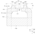
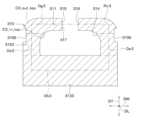
- the second core 210 includes a second gap forming portion 211 , a second easy shaft portion 212 , a second hard shaft portion 213 and a second core hole 214 .
- the second gap forming portion 211 is formed in a plate shape extending in the width direction DW. Moreover, the second gap forming portion 211 is separated from the second bus bar 200 in the thickness direction DT. Further, a second lateral outer corner portion C2_out_top, which is a corner portion on the outer side in the width direction DW of the second gap forming portion 211, has an R shape. Also, the second laterally outer corner C2_out_top and the first laterally outer corner C1_out_top face each other in the width direction DW. Furthermore, the second gap forming portion 211 includes a third core end face 215 , a fourth core end face 216 and a second gap 217 .
- the third core end face 215 overlaps the projected fourth core end face 216 when the fourth core end face 216 is projected in the width direction DW.
- a second gap 217 is a space defined by the third core end surface 215 and the fourth core end surface 216 . Further, second gap 217 communicates with second core hole 214 and the outside of second core 210 .
- the surface of the second plate portion 201 facing the third core end surface 215 and the fourth core end surface 216 in the thickness direction DT is defined as a second plate surface S2.
- a portion of the second plate surface S2 overlapping the projected third core end surface 215 when the third core end surface 215 is projected onto the second plate surface S2 in the thickness direction DT is referred to as a third projected portion Ps3.
- a portion of the second plate surface S2 overlapping the projected fourth core end surface 216 when the fourth core end surface 216 is projected onto the second plate surface S2 in the thickness direction DT is referred to as a fourth projected portion Ps4.
- the area of the second plate surface S2 defined by the third projection part Ps3 and the fourth projection part Ps4 is defined as a second area R2.
- a second recess 218 recessed in the thickness direction DT from at least a portion of the second region R2 is formed. Also, the second recess 218 is formed in a rectangular shape. In addition, the second recessed portion 218 is not limited to being formed in a rectangular shape, and may be formed in a polygonal shape or a circular shape.
- the second easy shaft portion 212 is connected to the second gap forming portion 211 . Further, the second easy shaft portion 212 extends in the thickness direction DT from the boundary portion between the second easy shaft portion 212 and the second gap forming portion 211 . Further, the inner second lateral inner corner C2_in_top at the boundary between the second easy shaft portion 212 and the second gap forming portion 211 has an R shape. Also, the second easy shaft portion 212 is separated from the second bus bar 200 in the width direction DW.
- the second hard shaft portion 213 is connected to the second easy shaft portion 212 . Furthermore, the second hard shaft portion 213 extends in the width direction DW. Further, the magnetic permeability of the second hard shaft portion 213 is lower than the magnetic permeability of the second easy shaft portion 212 . Furthermore, the saturation magnetic flux density of the second hard shaft portion 213 is smaller than the saturation magnetic flux density of the second easy shaft portion 212 . Further, the length of the second hard shaft portion 213 in the thickness direction DT is longer than the length of the second easy shaft portion 212 in the width direction DW.
- the second core hole 214 is a space formed by the second gap forming portion 211, the second easy shaft portion 212 and the second hard shaft portion 213. A portion of the second plate portion 201 of the second bus bar 200 is inserted into the second core hole 214 .
- the second detector 220 is arranged in the second gap 217 . Therefore, when the third core end face 215 is projected in the width direction DW, the second detector 220 overlaps the projected third core end face 215 . Furthermore, the second detector 220 overlaps the projected fourth core end surface 216 when the fourth core end surface 216 is projected in the width direction DW. Also, the second detection unit 220 has, for example, a Hall element, a TMR element, a GMR element, and an AMR element (not shown). With these elements, the second detection section 220 detects the intensity of the magnetic field applied to the second detection section 220 in the width direction DW. Furthermore, the second detection unit 220 outputs a signal corresponding to the strength of the detected magnetic field to the outside. The second lead wire 230 is connected to the second detector 220 .
- the third sensor 30 has a third busbar 300 , a third core 310 , a third detector 320 and a third lead wire 330 .
- the third bus bar 300 is made of copper or the like and formed into a plate shape. Moreover, the surface of the third bus bar 300 is plated to prevent the surface from being oxidized, if necessary. Furthermore, third bus bar 300 has third plate portion 301 , fifth extension portion 302 and sixth extension portion 303 .
- the third plate portion 301 includes a third bolt hole 304 .
- a bolt (not shown) is inserted into the third bolt hole 304 and the hole provided in the inverter. Thereby, the third plate portion 301 is connected to a part of the inverter.
- the fifth extension portion 302 is connected to the side of the third plate portion 301 opposite to the third bolt hole 304 . Also, the fifth extension portion 302 extends in the thickness direction DT from the boundary portion between the fifth extension portion 302 and the third plate portion 301 .
- the sixth extension portion 303 is connected to the opposite side of the fifth extension portion 302 to the third plate portion 301 . Also, the sixth extension portion 303 extends in the longitudinal direction DL from the boundary portion between the sixth extension portion 303 and the fifth extension portion 302 . Furthermore, the sixth extension 303 is connected to part of the inverter by being welded to the part of the inverter.
- the third core 310 is made of a soft magnetic material such as permalloy or a grain-oriented electrical steel sheet and is formed in a C shape.
- the third core 310 is formed by bending a plate-like soft magnetic material into a C shape.
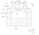
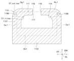
- the third core 310 includes a third gap forming portion 311 , a third easy shaft portion 312 , a third hard shaft portion 313 and a third core hole 314 .
- the third gap forming portion 311 is formed in a plate shape extending in the width direction DW. Also, the third gap forming portion 311 is separated from the third bus bar 300 in the thickness direction DT. Further, a third laterally outer corner portion C3_out_top, which is an outer corner portion in the width direction DW of the third gap forming portion 311, has an R shape. Also, the third laterally outer corner portion C3_out_top and the second laterally outer corner portion C2_out_top face each other in the width direction DW. Also, the third gap forming portion 311 includes a fifth core end face 315 , a sixth core end face 316 and a third gap 317 .
- the fifth core end face 315 overlaps the projected sixth core end face 316 when the sixth core end face 316 is projected in the width direction DW.
- a third gap 317 is a space defined by the fifth core end surface 315 and the sixth core end surface 316 . Furthermore, the third gap 317 communicates with the outside of the third core hole 314 and the third core 310 .
- the surface of the third plate portion 301 facing the fifth core end surface 315 and the sixth core end surface 316 in the thickness direction DT is defined as a third plate surface S3.
- a portion of the third plate surface S3 overlapping the projected fifth core end surface 315 when the fifth core end surface 315 is projected onto the third plate surface S3 in the thickness direction DT is referred to as a fifth projected portion Ps5.
- a portion of the third plate surface S3 that overlaps the projected sixth core end surface 316 when the sixth core end surface 316 is projected onto the third plate surface S3 in the thickness direction DT is referred to as a sixth projected portion Ps6.
- a region of the third plate surface S3 defined by the fifth projection portion Ps5 and the sixth projection portion Ps6 is defined as a third region R3.
- a third recess 318 recessed in the thickness direction DT from at least a portion of the third region R3 is formed.
- the third recess 318 is formed in a rectangular shape.
- the third recessed portion 318 is not limited to being formed in a rectangular shape, and may be formed in a polygonal shape or a circular shape.
- the third easy shaft portion 312 is connected to the third gap forming portion 311 . Further, the third easy shaft portion 312 extends in the thickness direction DT from the boundary portion between the third easy shaft portion 312 and the third gap forming portion 311 . Further, the inner third lateral inner corner C3_in_top at the boundary between the third easy shaft portion 312 and the third gap forming portion 311 has an R shape. Further, the third easy shaft portion 312 is separated from the third bus bar 300 in the width direction DW.
- the third hard shaft portion 313 is connected to the third easy shaft portion 312 . Further, the third hard shaft portion 313 extends in the width direction DW. Further, the magnetic permeability of the third hard shaft portion 313 is lower than the magnetic permeability of the third easy shaft portion 312 . Furthermore, the saturation magnetic flux density of the third hard shaft portion 313 is lower than the saturation magnetic flux density of the third easy shaft portion 312 . Also, the length of the third hard shaft portion 313 in the thickness direction DT is longer than the length of the third easy shaft portion 312 in the width direction DW.
- a third core hole 314 is a space formed by the third gap forming portion 311 , the third easy shaft portion 312 and the third hard shaft portion 313 .
- a portion of the third plate portion 301 of the third bus bar 300 is inserted into the third core hole 314 .
- the third detector 320 is arranged in the third gap 317 . Therefore, when the fifth core end face 315 is projected in the width direction DW, the third detector 320 overlaps the projected fifth core end face 315 . Furthermore, the third detector 320 overlaps the projected sixth core end face 316 when the sixth core end face 316 is projected in the width direction DW. Also, the third detection unit 320 has, for example, a Hall element, a TMR element, a GMR element, and an AMR element (not shown). With these elements, the third detector 320 detects the strength of the magnetic field in the width direction DW applied to the third detector 320 . Furthermore, the third detector 320 outputs a signal corresponding to the strength of the detected magnetic field to the outside. The third lead wire 330 is connected to the third detector 320 .
- the board 50 is a printed board. Further, the substrate 50 is connected to the first lead wire 130, the second lead wire 230 and the third lead wire 330 by soldering or the like.
- the terminal 60 is connected to the board 50 by soldering or the like. Furthermore, the terminal 60 is connected to a computing device (not shown).
- the case 70 is made of thermoplastic resin such as PBT.
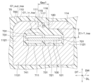
- the case 70 is formed by injection molding. Further, the case 70 has a housing portion 700 , a collar portion 701 and a fixing collar 702 .
- PBT is an abbreviation for Polybutylene Terephthalate.
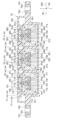
- the housing portion 700 is formed in a rectangular tubular shape.
- the accommodating portion 700 includes the first core 110, the second core 210, the third core 310, the first detection portion 120, the second detection portion 220, the third detection portion 320, the first lead wire 130, the second lead wire. 230 and a third lead 330 are accommodated.
- the housing portion 700 houses the board 50 and part of the terminal 60 . Further, the space of the housing portion 700 is filled with a resin such as urethane (not shown). As a result, the inside of the housing portion 700 is sealed, so that each component housed in the housing portion 700 is protected.
- the accommodation portion 700 includes the first extension portion 102 of the first bus bar 100, part of the second extension portion 103, third extension portion 202 of the second bus bar 200, and part of the fourth extension portion 203. , the fifth extension 302 and part of the sixth extension 303 of the third bus bar 300 . Also, the housing portion 700 includes a first opening 711 , a second opening 712 and a third opening 713 .
- the first opening 711 is inserted into the first core hole 114 .
- a part of the first plate portion 101 of the first bus bar 100 is inserted into the space of the first opening portion 711 .
- the first opening 711 includes a first facing surface 721 and a first protrusion 731 .
- the first opposing surface 721 faces the first plate portion 101 in the width direction DW and the thickness direction DT.
- the first protruding portion 731 protrudes from the first opposing surface 721 in the thickness direction DT and the width direction DW.
- the first projecting portion 731 is in contact with the first plate portion 101 . Thereby, the case 70 and the first bus bar 100 are positioned.
- a first space 741 is formed between the first opposing surface 721 and the first plate portion 101 .
- a portion of the second opening 712 is inserted into the second core hole 214 .
- a part of the second plate portion 201 of the second busbar 200 is inserted into the space of the second opening portion 712 .
- the second opening 712 includes a second facing surface 722 and a second protrusion 732 .
- the second facing surface 722 faces the second plate portion 201 in the width direction DW and the thickness direction DT.
- the second protruding portion 732 protrudes from the second opposing surface 722 in the thickness direction DT and the width direction DW.
- the second projecting portion 732 is in contact with the second plate portion 201 . Therefore, the case 70 and the second bus bar 200 are positioned.
- a second space 742 is formed between the second facing surface 722 and the second plate portion 201 .
- the third opening 713 includes a third facing surface 723 and a third protrusion 733 .
- the third facing surface 723 faces the third plate portion 301 in the width direction DW and the thickness direction DT.
- the third protruding portion 733 protrudes from the third facing surface 723 in the thickness direction DT and the width direction DW.
- the third projecting portion 733 is in contact with the third plate portion 301 . Thereby, the case 70 and the third bus bar 300 are positioned.
- a third space 743 is formed between the third facing surface 723 and the third plate portion 301 .
- the flange portion 701 protrudes in the width direction DW from a portion of the accommodation portion 700 on the width direction DW side.
- Collar 701 also includes a collar hole 704 .
- the flange hole 704 communicates with the outside in the thickness direction DT.
- a fixing collar 702 is inserted into the flange hole 704 . By inserting an external shaft (not shown) into the fixing collar 702, the case 70 is connected to the outside, thereby fixing the current sensor 5 to the outside.
- the current sensor 5 of the first embodiment is configured as described above. Next, the detection of the three-phase alternating current of the inverter by the current sensor 5 will be described.
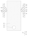
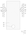
- the first plate portion 101 of the first bus bar 100 in the first sensor 10 is connected to part of the inverter. Also, the second extension portion 103 of the first bus bar 100 is connected to a part of the inverter. Therefore, the alternating current from the inverter flows through the first plate portion 101 . At this time, due to the alternating current flowing through the first plate portion 101, a magnetic field is generated in the circumferential direction around the axis extending in the longitudinal direction DL while passing through the first plate portion 101. FIG. Also, due to the generated magnetic field, the lines of magnetic force pass through the first core 110 , and thus pass through the first gap 117 . Therefore, the magnetic lines of force pass through the first detection section 120 .
- the first detector 120 detects the strength of the magnetic field in the width direction DW. Thereby, the first detection unit 120 detects the current from the inverter corresponding to the strength of this magnetic field. The first detector 120 also outputs a signal corresponding to the strength of the detected magnetic field to an external computing device (not shown) via the first lead wire 130 , the substrate 50 and the terminal 60 . This arithmetic unit calculates the current from the inverter based on the signal from the first detection section 120 .
- the magnetic field leaking from the first gap 117 enters the first plate portion 101, and the change in the frequency of the alternating current of the inverter causes the magnetic field to change over time.
- An induced electromotive force is generated in the opposite direction.
- the magnetic field applied to the first gap 117 changes due to the magnetic field generated by the current flowing through the first plate portion 101 due to the induced electromotive force. Therefore, an error occurs in the current detected by the current sensor 5 .
- the frequency of the alternating current of the inverter increases, the current flowing through the surface of the first plate portion 101 due to the induced electromotive force increases due to the skin effect, so the magnetic field applied to the first gap 117 changes. easier.
- the first recess 118 is formed in the first region R ⁇ b>1 of the first plate portion 101 , so the first plate portion 101 is easily separated from the first gap 117 . Therefore, since the lines of magnetic force entering the first plate portion 101 through the first gap 117 are suppressed, the generation of the induced electromotive force in the direction opposite to the direction of the current flowing through the first plate portion 101 is suppressed. Therefore, errors in the current detected by the current sensor 5 are less likely to occur, and the frequency characteristics of the current sensor 5 are improved.
- the first sensor 10 detects one phase of the three-phase alternating current of the inverter.
- the second sensor 20 like the first sensor 10, detects one phase of the three-phase alternating current of the inverter. Therefore, in the description of the second sensor 20 , the first sensor 10 is read as the second sensor 20 .
- the first busbar 100 is read as the second busbar 200 .
- the first plate portion 101 can be read as the second plate portion 201 .
- the second extension 103 is read as the fourth extension 203 .
- the first core 110 is read as the second core 210 .
- the first gap 117 is read as the second gap 217 .
- the first detection section 120 is read as the second detection section 220 .
- the first lead wire 130 is read as the second lead wire 230 .
- the first region R1 is read as the second region R2.
- the first recess 118 is read as the second recess 218 .
- the third sensor 30 detects one phase of the three-phase alternating current of the inverter. Therefore, in the description of the third sensor 30 , the first sensor 10 can be read as the third sensor 30 .
- the first busbar 100 is read as the third busbar 300 .
- the first plate portion 101 can be read as the third plate portion 301 .
- the second extension 103 is read as the sixth extension 303 .
- the first core 110 is read as the third core 310 .
- the first gap 117 is read as the third gap 317 .
- the first detector 120 can be read as the third detector 320 .
- the first lead wire 130 is read as the third lead wire 330 .
- the first region R1 is read as the third region R3.
- the first recess 118 can be read as the third recess 318 .
- the current sensor 5 detects the 3-phase alternating current of the inverter. Next, in the current sensor 5, improvement in frequency characteristics will be described.
- the magnetic field leaking from the core gap penetrates into the busbar, and the magnetic field changes with time due to the change in the frequency of the alternating current.
- An induced electromotive force is generated in the direction opposite to the direction of .
- the magnetic field applied to the core gap changes due to the magnetic field generated by the current flowing through the busbar due to the induced electromotive force. Therefore, an error occurs in the current detected by the comparison current sensor. Therefore, the frequency characteristic of the current sensor for comparison is degraded.
- the current sensor 5 detects the alternating current of the inverter. Further, the current sensor 5 includes a first bus bar 100, a second bus bar 200, a third bus bar 300, a first core 110, a second core 210, a third core 310, a first detector 120, A second detection unit 220 and a third detection unit 320 are provided. First bus bar 100, second bus bar 200 and third bus bar 300 are formed in a plate shape.
- the first core 110 has a first core hole 114 and a first gap forming portion 111 .
- First bus bar 100 is inserted into first core hole 114 .
- First gap forming portion 111 includes first core end face 115 , second core end face 116 and first gap 117 .
- the first core end surface 115 faces the width direction DW.
- the second core end face 116 faces the first core end face 115 in the width direction DW.
- a first gap 117 is formed by the first core end face 115 and the second core end face 116 and communicates with the first core hole 114 and the outside.
- the second core 210 has a second core hole 214 and a second gap forming portion 211 .
- a second bus bar 200 is inserted into the second core hole 214 .
- the second gap forming portion 211 includes a third core end face 215 , a fourth core end face 216 and a second gap 217 .
- the third core end surface 215 faces the width direction DW.
- the fourth core end face 216 faces the third core end face 215 in the width direction DW.
- a second gap 217 is formed by the third core end surface 215 and the fourth core end surface 216 and communicates with the second core hole 214 and the outside.
- the third core 310 has a third core hole 314 and a third gap forming portion 311 .
- the third bus bar 300 is inserted into the third core hole 314 .
- Third gap forming portion 311 includes fifth core end face 315 , sixth core end face 316 and third gap 317 .
- the fifth core end surface 315 faces the width direction DW.
- the sixth core end face 316 faces the fifth core end face 315 in the width direction DW.
- a third gap 317 is formed by the fifth core end surface 315 and the sixth core end surface 316 and communicates with the third core hole 314 and the outside.
- the first bus bar 100 has a first projection portion Ps1, a second projection portion Ps2, a first region R1, and a first concave portion 118.
- the first projected portion Ps1 is a portion of the first bus bar 100 that overlaps the projected first core end surface 115 when the first core end surface 115 is projected onto the first bus bar 100 in the thickness direction DT.
- Second projected portion Ps2 is a portion of first bus bar 100 overlapping second core end face 116 when second core end face 116 is projected onto first bus bar 100 in thickness direction DT.
- the first region R1 is the region between the first projection part Ps1 and the second projection part Ps2.
- the first recess 118 is recessed in the thickness direction DT from the first region R1.
- the second bus bar 200 has a third projected portion Ps3, a fourth projected portion Ps4, a second region R2, and a second concave portion 218.
- Third projected portion Ps3 is a portion of second bus bar 200 that overlaps projected third core end face 215 when third core end face 215 is projected onto second bus bar 200 in thickness direction DT.
- the fourth projected portion Ps4 is a portion of the second bus bar 200 that overlaps the projected fourth core end surface 216 when the fourth core end surface 216 is projected onto the second bus bar 200 in the thickness direction DT.
- the second region R2 is the region between the third projection part Ps3 and the fourth projection part Ps4.
- the second recessed portion 218 is recessed in the thickness direction DT from the second region R2.
- the third bus bar 300 has a fifth projected portion Ps5, a sixth projected portion Ps6, a third region R3, and a third concave portion 318.
- Fifth projected portion Ps5 is a portion of third bus bar 300 that overlaps projected fifth core end face 315 when fifth core end face 315 is projected onto third bus bar 300 in thickness direction DT.
- Sixth projected portion Ps6 is a portion of third bus bar 300 that overlaps projected sixth core end face 316 when sixth core end face 316 is projected onto third bus bar 300 in thickness direction DT.
- the third region R3 is the region between the fifth projection part Ps5 and the sixth projection part Ps6.
- the third recessed portion 318 is recessed in the thickness direction DT from the third region R3.
- the first busbar 100, the second busbar 200 and the third busbar 300 correspond to busbars.
- the first core 110, the second core 210 and the third core 310 correspond to cores.
- the first detection unit 120, the second detection unit 220 and the third detection unit 320 correspond to detection units.
- the first core hole 114, the second core hole 214 and the third core hole 314 correspond to core holes.
- the first gap forming portion 111, the second gap forming portion 211, and the third gap forming portion 311 correspond to gap forming portions.
- the first core end face 115, the third core end face 215 and the fifth core end face 315 correspond to the first end face.
- the second core end face 116, the fourth core end face 216 and the sixth core end face 316 correspond to the second end face.
- the first gap 117, the second gap 217 and the third gap 317 correspond to gaps.
- the third projection part Ps3 and the fifth projection part Ps5 correspond to the first projection part Ps1.
- the fourth projection part Ps4 and the sixth projection part Ps6 correspond to the second projection part Ps2.
- the first region R1, the second region R2 and the third region R3 correspond to regions.
- the first recess 118, the second recess 218 and the third recess 318 correspond to recesses.
- the first concave portion 118 makes it easier for the first plate portion 101 to separate from the first gap 117 . Therefore, the lines of magnetic force entering the first plate portion 101 through the first gap 117 are suppressed.
- the second recess 218 allows the second plate portion 201 to be easily separated from the second gap 217 . This suppresses the lines of magnetic force that enter the second plate portion 201 through the second gap 217 .
- the third recess 318 allows the third plate portion 301 to be easily separated from the third gap 317 . Therefore, the lines of magnetic force that enter the third plate portion 301 through the third gap 317 are suppressed.
- the current sensor 5 also has the following effects.
- the magnetic permeability of the first hard shaft portion 113 is smaller than the magnetic permeability of the first easy shaft portion 112
- the magnetic permeability of the first easy shaft portion 112 is 1 larger than the magnetic permeability of the hard-axis portion 113 .
- the linear region of the magnetic flux density of the first easy axis portion 112 with respect to the strength of the magnetic field becomes larger than the linear region of the magnetic flux density of the first hard axis portion 113 with respect to the strength of the magnetic field. . Therefore, since the magnetic saturation of the first easy shaft portion 112 is suppressed, the lengths of the first easy shaft portion 112 in the width direction DW and the longitudinal direction DL can be reduced.
- the magnetic permeability of the second easy shaft portion 212 is higher than the magnetic permeability of the second hard shaft portion 213 .
- the magnetic saturation of the second easy shaft portion 212 is suppressed, so that the lengths of the second easy shaft portion 212 in the width direction DW and the longitudinal direction DL can be reduced.
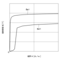
- the magnetic permeability of the third easy shaft portion 312 is greater than the magnetic permeability of the third hard shaft portion 313 . Therefore, since the magnetic saturation of the third easy shaft portion 312 is suppressed, the lengths of the third easy shaft portion 312 in the width direction DW and the longitudinal direction DL can be reduced. Therefore, the physical size of the current sensor 5 can be reduced. In FIG.
- Be1 indicates the magnetic flux density of the first easy axis portion 112 with respect to the strength of the magnetic field.
- Bd1 indicates the magnetic flux density of the first hard-axis portion 113 with respect to the strength of the magnetic field.
- the first easy shaft portion 112, the second easy shaft portion 212 and the third easy shaft portion 312 correspond to the core lateral portion.
- the first hard shaft portion 113, the second hard shaft portion 213, and the third hard shaft portion 313 correspond to the core bottom portion.
- the saturation magnetic flux density of the first easy shaft portion 112 is higher than that of the first hard shaft portion 113 .
- the linear region of the magnetic flux density of the first easy axis portion 112 with respect to the strength of the magnetic field becomes larger than the linear region of the magnetic flux density of the first hard axis portion 113 with respect to the strength of the magnetic field. Therefore, since the magnetic saturation of the first easy shaft portion 112 is suppressed, the lengths of the first easy shaft portion 112 in the width direction DW and the longitudinal direction DL can be reduced.
- the saturation magnetic flux density of the second easy shaft portion 212 is higher than the saturation magnetic flux density of the second hard shaft portion 213 .
- the magnetic saturation of the second easy shaft portion 212 is suppressed, so that the lengths of the second easy shaft portion 212 in the width direction DW and the longitudinal direction DL can be reduced.
- the saturation magnetic flux density of the third easy shaft portion 312 is higher than the saturation magnetic flux density of the third hard shaft portion 313 . Therefore, since the magnetic saturation of the third easy shaft portion 312 is suppressed, the lengths of the third easy shaft portion 312 in the width direction DW and the longitudinal direction DL can be reduced. Therefore, the physical size of the current sensor 5 can be reduced.
- the length of the first hard shaft portion 113 in the thickness direction DT is equal to or greater than the length of the first easy shaft portion 112 in the width direction DW.
- the magnetic flux density applied to the first hard shaft portion 113 is lower than the magnetic flux density applied to the first easy shaft portion 112 . Therefore, magnetic saturation of the first hard shaft portion 113 is suppressed.
- the length in the thickness direction DT of the second hard shaft portion 213 is equal to or greater than the length in the width direction DW of the second easy shaft portion 212 .
- the magnetic flux density applied to the second hard shaft portion 213 is lower than the magnetic flux density applied to the second easy shaft portion 212 . Therefore, magnetic saturation of the second hard shaft portion 213 is suppressed.
- the length in the thickness direction DT of the third hard shaft portion 313 is equal to or greater than the length in the width direction DW of the third easy shaft portion 312 .
- the magnetic flux density applied to the third hard shaft portion 313 is lower than the magnetic flux density applied to the third easy shaft portion 312 . Therefore, magnetic saturation of the third hard shaft portion 313 is suppressed.
- first hard-axis portion 113 since magnetic saturation of first hard-axis portion 113, second hard-axis portion 213, and third hard-axis portion 313 is suppressed, the intensity of magnetism detected by current sensor 5 with respect to the current from the inverter is reduced. Increased range. As a result, the range of magnitude of current detected by the current sensor 5 is widened.
- the current sensor 5 further includes a case 70 .
- Case 70 houses second core 210 , second core 210 and third core 310 .
- the case 70 has a first opening 711 , a second opening 712 and a third opening 713 .
- the first opening 711 is inserted into the first core hole 114 and the first bus bar 100 is inserted therein.
- the first opening 711 includes a first facing surface 721 and a first protrusion 731 .
- the first facing surface 721 faces the first plate portion 101 .
- the first projecting portion 731 is in contact with the first bus bar 100 by projecting from the first facing surface 721 toward the first bus bar 100 .
- a first space 741 is formed between the first facing surface 721 and the first bus bar 100 .
- Second opening 712 is inserted into second core hole 214 and into second bus bar 200 .
- the second opening 712 includes a second facing surface 722 and a second protrusion 732 .
- the second facing surface 722 faces the second plate portion 201 .
- the second projecting portion 732 is in contact with the second bus bar 200 by projecting from the second facing surface 722 toward the second bus bar 200 .
- a second space 742 is formed between the second facing surface 722 and the second plate portion 201 .
- the third opening 713 is inserted into the third core hole 314 and the third bus bar 300 is inserted therein.
- the third opening 713 includes a third facing surface 723 and a third protrusion 733 .
- the third facing surface 723 faces the third plate portion 301 .
- Third projecting portion 733 is in contact with third bus bar 300 by projecting from third opposing surface 723 toward third bus bar 300 . Furthermore, a third space 743 is formed between the third facing surface 723 and the third bus bar 300 . Note that the first opening 711, the second opening 712, and the third opening 713 correspond to openings. The first opposing surface 721, the second opposing surface 722 and the third opposing surface 723 correspond to the opposing surfaces. The first projecting portion 731, the second projecting portion 732 and the third projecting portion 733 correspond to projecting portions.
- the first bus bar 100, the second bus bar 200 and the third bus bar 300 generate heat due to the current flowing through the first bus bar 100, the second bus bar 200 and the third bus bar 300.
- the first space 741 , the second space 742 and the third space 743 are formed by the first projecting portion 731 , the second projecting portion 732 and the third projecting portion 733 .
- first projecting portion 731 is in contact with the first plate portion 101, the case 70 and the first bus bar 100 are positioned. This reduces positional variations between the case 70 and the first bus bar 100 .
- second projecting portion 732 is in contact with the second plate portion 201, the case 70 and the second bus bar 200 are positioned. Therefore, positional variations between the case 70 and the second bus bar 200 are reduced.
- the third projecting portion 733 is in contact with the third plate portion 301, so that the case 70 and the third bus bar 300 are positioned. This reduces positional variations between the case 70 and the third bus bar 300 .
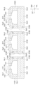
- the shapes of the first plate portion 101, the second plate portion 201 and the third plate portion 301 are different from those in the first embodiment. Other than these, it is the same as the first embodiment.
- the first plate portion 101 includes a first through hole 119 instead of the first concave portion 118 .
- the first through hole 119 penetrates from at least a portion of the first region R1 in the thickness direction DT.
- the second plate portion 201 includes a second through hole 219 instead of the second concave portion 218 .
- the second through hole 219 penetrates from at least a portion of the second region R2 in the thickness direction DT.
- the third plate portion 301 includes a third through hole 319 instead of the third concave portion 318 .
- the third through hole 319 penetrates from at least a portion of the third region R3 in the thickness direction DT.
- the first through-hole 119, the second through-hole 219 and the third through-hole 319 are formed in a rectangular shape.
- first through hole 119, the second through hole 219, and the third through hole 319 correspond to through holes. Furthermore, the first through-hole 119, the second through-hole 219, and the third through-hole 319 are not limited to being formed in a rectangular shape, and may be formed in a polygonal shape or a circular shape.
- the current sensor 5 of the second embodiment is configured as described above. Also in this second embodiment, the same effect as in the first embodiment is obtained.
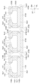
- the shapes of a first gap forming portion 111, a second gap forming portion 211 and a third gap forming portion 311 are different from those of the first embodiment. Other than these, it is the same as the first embodiment.
- the first gap forming portion 111 includes a first slanted surface 151 and a second slanted surface 152 in addition to the first core end surface 115 , the second core end surface 116 and the first gap 117 .
- the first inclined surface 151 is connected to the edge of the first core end surface 115 . Also, the first inclined surface 151 extends from the edge of the first core end surface 115 in a direction crossing the first core end surface 115 . Thereby, the first inclined surface 151 is inclined with respect to the first core end surface 115 in the direction away from the first gap 117 .
- the second inclined surface 152 is connected to the edge of the second core end surface 116 . Further, the second inclined surface 152 extends from the edge of the second core end surface 116 in a direction crossing the second core end surface 116 . Therefore, the second inclined surface 152 is inclined with respect to the second core end surface 116 in the direction away from the second gap 217 .
- the second gap forming portion 211 includes a third slanted surface 251 and a fourth slanted surface 252 in addition to the third core end surface 215 , the fourth core end surface 216 and the second gap 217 .
- the third inclined surface 251 is connected to the edge of the third core end surface 215 . Also, the third inclined surface 251 extends from the edge of the third core end surface 215 in a direction crossing the third core end surface 215 . Thereby, the third inclined surface 251 is inclined with respect to the third core end surface 215 in the direction away from the second gap 217 .
- the fourth inclined surface 252 is connected to the edge of the fourth core end surface 216. Furthermore, the fourth inclined surface 252 extends from the edge of the fourth core end surface 216 in a direction crossing the fourth core end surface 216 . Therefore, the fourth inclined surface 252 is inclined with respect to the fourth core end surface 216 in the direction away from the second gap 217 .
- the third gap forming portion 311 includes a fifth inclined surface 351 and a sixth inclined surface 352 in addition to the fifth core end surface 315, the sixth core end surface 316 and the third gap 317.
- the fifth inclined surface 351 is connected to the edge of the fifth core end surface 315 . Also, the fifth inclined surface 351 extends from the edge of the fifth core end surface 315 in a direction crossing the fifth core end surface 315 . Thereby, the fifth inclined surface 351 is inclined with respect to the fifth core end surface 315 in the direction away from the third gap 317 .
- the sixth inclined surface 352 is connected to the edge of the sixth core end surface 316. Furthermore, the sixth inclined surface 352 extends from the edge of the sixth core end surface 316 in a direction crossing the sixth core end surface 316 . Therefore, the sixth inclined surface 352 is inclined with respect to the sixth core end surface 316 in the direction away from the third gap 317 .
- the current sensor 5 of the third embodiment is configured as described above. Also in the third embodiment, the same effects as in the first embodiment are obtained. In addition, the third embodiment also has the effects described below.
- the corner of the second gap forming portion 211 is easily separated from the second gap 217 by the third inclined surface 251 and the fourth inclined surface 252 . Therefore, the number of extra magnetic lines of force passing through the second gap 217 from the corner of the second gap forming portion 211 is reduced compared to when the third inclined surface 251 and the fourth inclined surface 252 are not provided. Magnetic saturation of the second gap forming portion 211 is thereby suppressed. Furthermore, the fifth inclined surface 351 and the sixth inclined surface 352 facilitate the separation of the corner of the third gap forming portion 311 from the third gap 317 .
- the number of extra magnetic lines of force passing through the third gap 317 from the corner of the third gap forming portion 311 is reduced compared to the case where the fifth inclined surface 351 and the sixth inclined surface 352 are not provided. Magnetic saturation of the third gap forming portion 311 is thereby suppressed. Therefore, since the magnetic saturation of the first gap forming portion 111, the second gap forming portion 211 and the third gap forming portion 311 is suppressed, the intensity of the magnetism detected by the current sensor 5 with respect to the current from the inverter is reduced. Increased range. Therefore, the range of magnitude of current detected by the current sensor 5 is widened.
- the first inclined surface 151, the third inclined surface 251, and the fifth inclined surface 351 are connected to the edge of the first end surface and extend from the edge of the first end surface in a direction away from the gap. handle.
- the second inclined surface 152, the fourth inclined surface 252 and the sixth inclined surface 352 are connected to the edge of the second end surface and extend from the edge of the second end surface in a direction away from the gap. handle.
- the angle formed by the first inclined surface 151 and the first core end surface 115 may be 90 degrees.
- the angle formed by the second inclined surface 152 and the second core end surface 116 may be 90 degrees.
- the angle formed by the third inclined surface 251 and the third core end surface 215 may be 90 degrees.
- the angle formed by the fourth inclined surface 252 and the fourth core end surface 216 may be 90 degrees. Furthermore, the angle between the fifth inclined surface 351 and the fifth core end surface 315 may be 90 degrees. Also, the angle formed by the sixth inclined surface 352 and the sixth core end surface 316 may be 90 degrees.
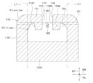
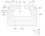
- the first core 110 includes a first core lateral portion 1121 and a first core bottom portion 1131 instead of the first easy shaft portion 112 and the first hard shaft portion 113 .
- the first core horizontal part 1121 is connected to the first gap forming part 111 . Further, the first core horizontal portion 1121 extends in the thickness direction DT from the boundary portion between the first core horizontal portion 1121 and the first gap forming portion 111 . Further, the inner first lateral inner corner C1_in_top at the boundary between the first core lateral portion 1121 and the first gap forming portion 111 has an R shape. Also, the first core horizontal portion 1121 is separated from the first bus bar 100 in the width direction DW.
- the first core bottom portion 1131 is connected to the first core lateral portion 1121 . Furthermore, the first core bottom portion 1131 extends in the width direction DW. Further, the magnetic permeability of first core bottom portion 1131 is higher than the magnetic permeability of first core horizontal portion 1121 . Furthermore, the saturation magnetic flux density of first core bottom portion 1131 is higher than the saturation magnetic flux density of first core lateral portion 1121 . Also, the length in the thickness direction DT of the first core bottom portion 1131 is shorter than the length in the width direction DW of the first core lateral portion 1121 .
- First core hole 114 is a space formed by first gap forming portion 111 , first core lateral portion 1121 and first core bottom portion 1131 .
- the second core 210 includes a second core lateral portion 2122 and a second core bottom portion 2132 instead of the second easy shaft portion 212 and the second hard shaft portion 213 .
- the second core horizontal part 2122 is connected to the second gap forming part 211 . Also, the second core lateral portion 2122 extends in the thickness direction DT. Further, the inner second lateral inner corner C2_in_top at the boundary between the second core lateral portion 2122 and the second gap forming portion 211 has an R shape. Also, the second core horizontal portion 2122 is separated from the second bus bar 200 in the width direction DW.
- the second core bottom portion 2132 is connected to the second core lateral portion 2122 . Further, the second core bottom portion 2132 extends in the width direction DW. Further, the magnetic permeability of the second core bottom portion 2132 is higher than the magnetic permeability of the second core horizontal portion 2122 . Furthermore, the saturation magnetic flux density of the second core bottom portion 2132 is higher than the saturation magnetic flux density of the second core lateral portion 2122 . Also, the length in the thickness direction DT of the second core bottom portion 2132 is shorter than the length in the width direction DW of the second core lateral portion 2122 . Second core hole 214 is a space formed by second gap forming portion 211 , second core lateral portion 2122 and second core bottom portion 2132 .
- the third core 310 includes a third core lateral portion 3123 and a third core bottom portion 3133 instead of the third easy shaft portion 312 and the third hard shaft portion 313 .
- the third core horizontal portion 3123 is connected to the third gap forming portion 311 . Further, the third core horizontal portion 3123 extends in the thickness direction DT from the boundary portion between the third core horizontal portion 3123 and the third gap forming portion 311 . Further, the inner third lateral inner corner C3_in_top at the boundary between the third core lateral portion 3123 and the third gap forming portion 311 has an R shape. Also, the third core lateral portion 3123 is separated from the third bus bar 300 in the width direction DW.
- the third core bottom portion 3133 is connected to the third core lateral portion 3123 . Furthermore, the third core bottom portion 3133 extends in the width direction DW. Further, the magnetic permeability of the third core bottom portion 3133 is higher than the magnetic permeability of the third core horizontal portion 3123 . Furthermore, the saturation magnetic flux density of the third core bottom portion 3133 is higher than the saturation magnetic flux density of the third core lateral portion 3123 . Also, the length in the thickness direction DT of the third core bottom portion 3133 is shorter than the length in the width direction DW of the third core lateral portion 3123 . Third core hole 314 is a space formed by third gap forming portion 311 , third core lateral portion 3123 and third core bottom portion 3133 .
- the current sensor 5 of the fourth embodiment is configured as described above. Also in this fourth embodiment, the same effect as in the first embodiment is obtained. In addition, the fourth embodiment also has the effects described below.
- the length of the first core bottom portion 1131 in the thickness direction DT is smaller than the length of the first core lateral portion 1121 in the width direction DW.
- the magnetic flux density applied to the first core horizontal portion 1121 is lower than the magnetic flux density applied to the first core bottom portion 1131 . Therefore, magnetic saturation of the first core horizontal portion 1121 is suppressed.
- the length of the second core bottom portion 2132 in the thickness direction DT is shorter than the length of the second core lateral portion 2122 in the width direction DW.
- the magnetic flux density applied to the second core lateral portion 2122 is lower than the magnetic flux density applied to the second core bottom portion 2132 . Therefore, magnetic saturation of the second core lateral portion 2122 is suppressed.
- the length of the third core bottom portion 3133 in the thickness direction DT is shorter than the length of the third core lateral portion 3123 in the width direction DW.
- the magnetic flux density applied to the third core horizontal portion 3123 is lower than the magnetic flux density applied to the third core bottom portion 3133 . Therefore, magnetic saturation of the third core horizontal portion 3123 is suppressed.
- the magnetic permeability of the first core horizontal portion 1121 is lower than the magnetic permeability of the first core bottom portion 1131 .
- the linear region of the magnetic flux density of the first core bottom portion 1131 with respect to the magnetic field strength becomes larger than the linear region of the magnetic flux density of the first core lateral portion 1121 with respect to the magnetic field strength. Therefore, since the magnetic saturation of the first core bottom portion 1131 is suppressed, the lengths of the first core bottom portion 1131 in the thickness direction DT and the longitudinal direction DL can be reduced.
- the magnetic permeability of the second core lateral portion 2122 is lower than the magnetic permeability of the second core bottom portion 2132 .
- a first core lateral portion 1121, a first core bottom portion 1131, a second core lateral portion 2122, a second core bottom portion 2132, a third core lateral portion 3123 and a third core bottom portion 3133 differs from the fourth embodiment. Other than these, it is the same as the fourth embodiment.
- the length of the first core bottom portion 1131 in the thickness direction DT and the length of the first core lateral portion 1121 in the width direction DW are the same. Further, the magnetic permeability of the first core horizontal portion 1121 and the magnetic permeability of the first core bottom portion 1131 are different. For example, the magnetic permeability of the first core horizontal portion 1121 and the magnetic permeability of the first core bottom portion 1131 are increased. It should be noted that the “same” here includes the manufacturing error range. Further, the magnetic permeability of first core horizontal portion 1121 may be small, and the magnetic permeability of first core bottom portion 1131 may be small.
- the length of the second core bottom portion 2132 in the thickness direction DT and the length of the second core lateral portion 2122 in the width direction DW are the same. Further, the magnetic permeability of the second core horizontal portion 2122 and the magnetic permeability of the second core bottom portion 2132 are different. For example, the magnetic permeability of the second core lateral portion 2122 is increased, and the magnetic permeability of the second core bottom portion 2132 is increased. The magnetic permeability of the second core horizontal portion 2122 may be lower than that of the second core bottom portion 2132 .
- the length of the third core bottom portion 3133 in the thickness direction DT and the length of the third core lateral portion 3123 in the width direction DW are the same. Further, the magnetic permeability of the third core horizontal portion 3123 and the magnetic permeability of the third core bottom portion 3133 are different. For example, the magnetic permeability of the third core horizontal portion 3123 is increased, and the magnetic permeability of the third core bottom portion 3133 is increased. Note that the magnetic permeability of the third core horizontal portion 3123 and the magnetic permeability of the third core bottom portion 3133 may be small.
- the current sensor 5 of the fifth embodiment is configured as described above. Also in this fifth embodiment, the same effect as in the fourth embodiment is obtained. In addition, the fifth embodiment also has the effects described below.
- the magnetic permeability of the first core horizontal portion 1121 and the magnetic permeability of the first core bottom portion 1131 are different, the magnetic permeability of either the first core horizontal portion 1121 or the first core bottom portion 1131 is larger.
- the linear region of the magnetic flux density with respect to the strength of the magnetic field can be increased in either the first core horizontal portion 1121 or the first core bottom portion 1131 . Therefore, magnetic saturation of either first core lateral portion 1121 or first core bottom portion 1131 is suppressed. Accordingly, either the first core horizontal portion 1121 or the first core bottom portion 1131 can be made smaller.
- the magnetic permeability of the second core horizontal portion 2122 and the magnetic permeability of the second core bottom portion 2132 are different, it is possible to increase the magnetic permeability of either the second core horizontal portion 2122 or the second core bottom portion 2132. can be done. As a result, the linear region of the magnetic flux density with respect to the strength of the magnetic field can be increased in either the second core lateral portion 2122 or the second core bottom portion 2132 . Therefore, magnetic saturation of either the second core lateral portion 2122 or the second core bottom portion 2132 is suppressed. Accordingly, either the second core horizontal portion 2122 or the second core bottom portion 2132 can be made smaller.
- the magnetic permeability of the third core horizontal portion 3123 and the magnetic permeability of the third core bottom portion 3133 are different, the magnetic permeability of either the third core horizontal portion 3123 or the third core bottom portion 3133 can be increased. can be done. As a result, the linear region of the magnetic flux density with respect to the strength of the magnetic field can be increased in either the third core horizontal portion 3123 or the third core bottom portion 3133 . Therefore, magnetic saturation of either the third core lateral portion 3123 or the third core bottom portion 3133 is suppressed. Accordingly, either the third core horizontal portion 3123 or the third core bottom portion 3133 can be made smaller.
- the first core 110 includes a first core lateral portion 1121 and a first core bottom portion 1131 instead of the first easy shaft portion 112 and the first hard shaft portion 113 .
- the first core horizontal part 1121 is connected to the first gap forming part 111 . Further, the first core horizontal portion 1121 extends in the thickness direction DT from the boundary portion between the first core horizontal portion 1121 and the first gap forming portion 111 . Further, the inner first lateral inner corner C1_in_top at the boundary between the first core lateral portion 1121 and the first gap forming portion 111 has an R shape. Also, the first core horizontal portion 1121 is separated from the first bus bar 100 in the width direction DW. In addition, the 1st gap formation part 111 is separated from the 1st bus bar 100 in the thickness direction DT similarly to the above.
- the first core bottom portion 1131 is connected to the first core lateral portion 1121 . Furthermore, the first core bottom portion 1131 extends in the width direction DW. Further, the magnetic permeability of first core bottom portion 1131 is lower than the magnetic permeability of first core horizontal portion 1121 . Furthermore, the saturation magnetic flux density of first core bottom portion 1131 is lower than the saturation magnetic flux density of first core lateral portion 1121 . Also, the length in the thickness direction DT of the first core bottom portion 1131 is longer than the length in the width direction DW of the first core lateral portion 1121 . It should be noted that, similarly to the above, first core hole 114 is a space formed by first gap forming portion 111 , first core lateral portion 1121 and first core bottom portion 1131 .
- the second core 210 includes a second core lateral portion 2122 and a second core bottom portion 2132 instead of the second easy shaft portion 212 and the second hard shaft portion 213 .
- the second core horizontal portion 2122 is connected to the second gap forming portion 211 . Further, the second core horizontal portion 2122 extends in the thickness direction DT from the boundary portion between the second core horizontal portion 2122 and the second gap forming portion 211 . Further, the inner second lateral inner corner C2_in_top at the boundary between the second core lateral portion 2122 and the second gap forming portion 211 has an R shape. Also, the second core lateral portion 2122 is separated from the second bus bar 200 in the width direction DW. In addition, the 2nd gap formation part 211 is separated from the 2nd bus bar 200 in the thickness direction DT similarly to the above.
- the second core bottom portion 2132 is connected to the second core lateral portion 2122 . Further, the second core bottom portion 2132 extends in the width direction DW. Also, the magnetic permeability of the second core bottom portion 2132 is lower than the magnetic permeability of the second core horizontal portion 2122 . Furthermore, the saturation magnetic flux density of the second core bottom portion 2132 is lower than the saturation magnetic flux density of the second core lateral portion 2122 . Also, the length in the thickness direction DT of the second core bottom portion 2132 is longer than the length in the width direction DW of the second core lateral portion 2122 . It should be noted that, similarly to the above, the second core hole 214 is a space formed by the second gap forming portion 211 , the second core lateral portion 2122 and the second core bottom portion 2132 .
- the third core 310 includes a third core lateral portion 3123 and a third core bottom portion 3133 instead of the third easy shaft portion 312 and the third hard shaft portion 313 .
- the third core horizontal portion 3123 is connected to the third gap forming portion 311 . Further, the third core horizontal portion 3123 extends in the thickness direction DT from the boundary portion between the third core horizontal portion 3123 and the third gap forming portion 311 . Further, the inner third lateral inner corner C3_in_top at the boundary between the third core lateral portion 3123 and the third gap forming portion 311 has an R shape. Also, the third core lateral portion 3123 is separated from the third bus bar 300 in the width direction DW. In addition, the 3rd gap formation part 311 is separated from the 3rd bus bar 300 in the thickness direction DT similarly to the above.
- the third core bottom portion 3133 is connected to the third core lateral portion 3123 . Furthermore, the third core bottom portion 3133 extends in the width direction DW. Further, the magnetic permeability of the third core bottom portion 3133 is lower than the magnetic permeability of the third core horizontal portion 3123 . Furthermore, the saturation magnetic flux density of the third core bottom portion 3133 is lower than the saturation magnetic flux density of the third core lateral portion 3123 . Also, the length in the thickness direction DT of the third core bottom portion 3133 is longer than the length in the width direction DW of the third core lateral portion 3123 . In addition, the third core hole 314 is a space formed by the third gap forming portion 311 , the third core lateral portion 3123 and the third core bottom portion 3133 in the same manner as described above.
- the current sensor 5 of the sixth embodiment is configured as described above. Also in this sixth embodiment, the same effect as in the first embodiment is obtained. In addition, the sixth embodiment also has the effects described below.
- the first lateral inner corner C1_in_top, the second lateral inner corner C2_in_top and the third lateral inner corner C3_in_top are rounded.
- the magnetic path length inside each of first core 110, second core 210 and third core 310 is shortened, the length of each inside first core 110, second core 210 and third core 310 is reduced.
- the strength of the demagnetizing field increases. Therefore, the magnetic flux density of each of first core 110, second core 210 and third core 310 is suppressed. Therefore, magnetic saturation of each of first core 110, second core 210 and third core 310 is suppressed.
- the first gap forming portion 111 is separated from the first bus bar 100 in the thickness direction DT, and the first core lateral portion 1121 is separated from the first bus bar 100 in the width direction DW. This suppresses contact between first bus bar 100 and first core 110 .
- Second gap forming portion 211 is separated from second bus bar 200 in thickness direction DT, and second core lateral portion 2122 is separated from second bus bar 200 in width direction DW. Therefore, contact between second bus bar 200 and second core 210 is suppressed.
- third gap forming portion 311 is separated from third bus bar 300 in thickness direction DT, and third core lateral portion 3123 is separated from third bus bar 300 in width direction DW. This suppresses contact between third bus bar 300 and third core 310 .
- the first core 110 has a first bottom inside corner C1_in_btm in addition to the first lateral inside corner C1_in_top.
- First bottom inner corner portion C1_in_btm is an inner corner portion at the boundary between first core horizontal portion 1121 and first core bottom portion 1131 and is formed in an R shape.
- the first core bottom portion 1131 is separated from the first bus bar 100 in the thickness direction DT.
- the second core 210 has a second bottom inner corner C2_in_btm in addition to the second lateral inner corner C2_in_top.
- Second bottom inner corner C2_in_btm is an inner corner at the boundary between second core lateral portion 2122 and second core bottom portion 2132 and is formed in an R shape. Also, the second core bottom portion 2132 is separated from the second bus bar 200 in the thickness direction DT.
- the third core 310 has a third bottom inner corner C3_in_btm in addition to the third lateral inner corner C3_in_top.
- the third bottom inner corner portion C3_in_btm is an inner corner portion at the boundary portion between the third core horizontal portion 3123 and the third core bottom portion 3133 and is formed in an R shape. Also, the third core bottom portion 3133 is separated from the third bus bar 300 in the thickness direction DT.
- the current sensor 5 of the seventh embodiment is configured as described above. Also in the seventh embodiment, the same effect as in the sixth embodiment is obtained. In addition, the seventh embodiment also has the effects described below.
- the first bottom inner corner C1_in_btm, the second bottom inner corner C2_in_btm, and the third bottom inner corner C3_in_btm are rounded.
- the magnetic path length inside each of first core 110, second core 210 and third core 310 is shortened, the length of each inside first core 110, second core 210 and third core 310 is reduced.
- the strength of the demagnetizing field increases. Therefore, the magnetic flux density of each of first core 110, second core 210 and third core 310 is suppressed. Therefore, magnetic saturation of each of first core 110, second core 210 and third core 310 is suppressed.
- the first core bottom portion 1131 is separated from the first bus bar 100 in the thickness direction DT. This suppresses contact between first bus bar 100 and first core bottom portion 1131 .
- the second core bottom portion 2132 is separated from the second bus bar 200 in the thickness direction DT. Therefore, contact between second bus bar 200 and second core bottom portion 2132 is suppressed.
- the third core bottom portion 3133 is separated from the third bus bar 300 in the thickness direction DT. This suppresses contact between third bus bar 300 and third core bottom portion 3133 .
- the shapes of the first lateral inner corner portion C1_in_top and the first bottom inner corner portion C1_in_btm are different from those in the seventh embodiment.
- the shapes of the second lateral inner corner portion C2_in_top and the second bottom inner corner portion C2_in_btm are different from those of the seventh embodiment.
- the shapes of the third lateral inner corner C3_in_top and the third bottom inner corner C3_in_btm are different from those of the seventh embodiment. Other than these, it is the same as the seventh embodiment.
- First lateral inner corner portion C1_in_top is connected to the inner surface of first gap forming portion 111 and the inner surface of first core lateral portion 1121, and forms an inclined surface that is inclined with respect to width direction DW and thickness direction DT.
- First bottom inner corner portion C1_in_btm is connected to the inner surface of first core lateral portion 1121 and the inner surface of first core bottom portion 1131, and forms an inclined surface that is inclined with respect to width direction DW and thickness direction DT. .
- Second lateral inner corner portion C2_in_top is connected to the inner surface of second gap forming portion 211 and the inner surface of second core lateral portion 2122, and forms an inclined surface that is inclined with respect to width direction DW and thickness direction DT.
- the second bottom inner corner portion C2_in_btm is connected to the inner surface of the second core lateral portion 2122 and the inner surface of the second core bottom portion 2132, and forms an inclined surface that is inclined with respect to the width direction DW and the thickness direction DT. .
- Third lateral inner corner portion C3_in_top is connected to the inner surface of third gap forming portion 311 and the inner surface of third core lateral portion 3123, and forms an inclined surface that is inclined with respect to width direction DW and thickness direction DT.
- the third bottom inner corner portion C3_in_btm is connected to the inner surface of the third core lateral portion 3123 and the inner surface of the third core bottom portion 3133, and forms an inclined surface that is inclined with respect to the width direction DW and the thickness direction DT. .
- the current sensor 5 of the eighth embodiment is configured as described above. Also in this eighth embodiment, the same effects as those of the seventh embodiment are obtained.
- First core 110 includes first gap forming portion 111 and first core hole 114, and instead of first easy shaft portion 112 and first hard shaft portion 113, first core horizontal portion 1121 and first core bottom portion Including 1131.
- the first core horizontal part 1121 is connected to the first gap forming part 111 . Further, the first core horizontal portion 1121 extends in the thickness direction DT from the boundary portion between the first core horizontal portion 1121 and the first gap forming portion 111 . Note that, in the same manner as described above, the first lateral outer corner portion C1_out_top, which is the outer corner portion in the width direction DW of the first gap forming portion 111, has an R shape.
- the first core bottom portion 1131 is connected to the first core lateral portion 1121 . Furthermore, the first core bottom portion 1131 extends in the width direction DW. Further, the magnetic permeability of first core bottom portion 1131 is lower than the magnetic permeability of first core horizontal portion 1121 . Furthermore, the saturation magnetic flux density of first core bottom portion 1131 is lower than the saturation magnetic flux density of first core lateral portion 1121 . Also, the length in the thickness direction DT of the first core bottom portion 1131 is longer than the length in the width direction DW of the first core lateral portion 1121 . It should be noted that, similarly to the above, first core hole 114 is a space formed by first gap forming portion 111 , first core lateral portion 1121 and first core bottom portion 1131 .
- Second core 210 includes second gap forming portion 211 and second core hole 214, and has second core lateral portion 2122 and second core bottom portion instead of second easy shaft portion 212 and second hard shaft portion 213. 2132.
- the second core horizontal portion 2122 is connected to the second gap forming portion 211 . Further, the second core horizontal portion 2122 extends in the thickness direction DT from the boundary portion between the second core horizontal portion 2122 and the second gap forming portion 211 .
- the second lateral outer corner C2_out_top which is the outer corner in the width direction DW of the second gap forming portion 211, has an R shape. Also, the second laterally outer corner C2_out_top and the first laterally outer corner C1_out_top face each other in the width direction DW.
- the second core bottom portion 2132 is connected to the second core lateral portion 2122 . Further, the second core bottom portion 2132 extends in the width direction DW. Also, the magnetic permeability of the second core bottom portion 2132 is lower than the magnetic permeability of the second core horizontal portion 2122 . Furthermore, the saturation magnetic flux density of the second core bottom portion 2132 is lower than the saturation magnetic flux density of the second core lateral portion 2122 . Also, the length in the thickness direction DT of the second core bottom portion 2132 is longer than the length in the width direction DW of the second core lateral portion 2122 . It should be noted that, similarly to the above, the second core hole 214 is a space formed by the second gap forming portion 211 , the second core lateral portion 2122 and the second core bottom portion 2132 .
- Third core 310 includes third gap forming portion 311 and third core hole 314, and instead of third easy shaft portion 312 and third hard shaft portion 313, third core horizontal portion 3123 and third core bottom portion 3133 included.
- the third core horizontal portion 3123 is connected to the third gap forming portion 311 . Further, the third core horizontal portion 3123 extends in the thickness direction DT from the boundary portion between the third core horizontal portion 3123 and the third gap forming portion 311 . Note that, in the same manner as described above, the third lateral outer corner portion C3_out_top, which is the outer corner portion in the width direction DW of the third gap forming portion 311, has an R shape. Further, the third laterally outer corner C3_out_top and the second laterally outer corner C2_out_top face each other in the width direction DW.
- the third core bottom portion 3133 is connected to the third core lateral portion 3123 . Furthermore, the third core bottom portion 3133 extends in the width direction DW. Further, the magnetic permeability of the third core bottom portion 3133 is lower than the magnetic permeability of the third core horizontal portion 3123 . Furthermore, the saturation magnetic flux density of the third core bottom portion 3133 is lower than the saturation magnetic flux density of the third core lateral portion 3123 . Also, the length in the thickness direction DT of the third core bottom portion 3133 is longer than the length in the width direction DW of the third core lateral portion 3123 . In addition, the third core hole 314 is a space formed by the third gap forming portion 311 , the third core lateral portion 3123 and the third core bottom portion 3133 in the same manner as described above.
- the current sensor 5 of the ninth embodiment is configured as described above. Also in the ninth embodiment, the same effect as in the first embodiment is obtained. In addition, the ninth embodiment also has the effects described below.
- the first core 110, the second core 210 and the third core 310 are arranged in the order of the first core 110, the second core 210 and the third core 310 in the width direction DW. Also, the first lateral outer corner C1_out_top and the second lateral outer corner C2_out_top facing each other in the width direction DW are rounded. As a result, the maximum distance in the width direction DW between the first gap forming portion 111 and the second gap forming portion 211 becomes longer than when the R shape is not formed. Further, the second lateral outer corner C2_out_top and the third lateral outer corner C3_out_top facing each other in the width direction DW are rounded.
- the maximum distance in the width direction DW between the second gap forming portion 211 and the third gap forming portion 311 becomes longer than when the R shape is not formed.
- the magnetic resistance between the first core 110 and the second core 210 adjacent to each other and between the second core 210 and the third core 310 adjacent to each other increases. Therefore, magnetic paths are less likely to be formed in first core 110 and second core 210 adjacent to each other, and second core 210 and third core 310 adjacent to each other. Therefore, a decrease in magnetic resistance in the entirety of first core 110, second core 210, and third core 310 is suppressed. Therefore, an increase in the magnetic flux density of each of first core 110, second core 210 and third core 310 due to the influence of adjacent cores is suppressed. Magnetic saturation of each of the cores 310 is suppressed.
- the first core 110 has a first bottom outer corner C1_out_btm in addition to the first lateral outer corner C1_out_top.
- the first bottom outside corner portion C1_out_btm is the outside corner portion in the width direction DW of the first core bottom portion 1131 and is formed in an R shape.
- the second core 210 has a second bottom outer corner C2_out_btm in addition to the second lateral outer corner C2_out_top.
- the second bottom outside corner portion C2_out_btm is a corner portion on the outside in the width direction DW of the second core bottom portion 2132 and is formed in an R shape. Also, the second bottom outside corner portion C2_out_btm and the first bottom outside corner portion C1_out_btm face each other in the width direction DW.
- the third core 310 has a third bottom outer corner C3_out_btm in addition to the third lateral outer corner C3_out_top.
- the third bottom outside corner portion C3_out_btm is a corner portion on the outside in the width direction DW of the third core bottom portion 3133 and is formed in an R shape. Also, the third bottom outside corner C3_out_btm and the second bottom outside corner C2_out_btm face each other in the width direction DW.
- the current sensor 5 of the tenth embodiment is configured as described above.
- the tenth embodiment also has the same effect as the ninth embodiment.
- the tenth embodiment also has the effects described below.
- the first bottom outer corner C1_out_btm and the second bottom outer corner C2_out_btm facing each other in the width direction DW are rounded.
- the maximum distance in the width direction DW between the first core bottom portion 1131 and the second core bottom portion 2132 is increased compared to the case where the R shape is not formed.
- the second bottom outer corner C2_out_btm and the third bottom outer corner C3_out_btm facing each other in the width direction DW are rounded.
- the maximum distance in the width direction DW between the second core bottom portion 2132 and the third core bottom portion 3133 is increased compared to the case where the R shape is not formed.
- the magnetic resistance between the first core 110 and the second core 210 adjacent to each other and between the second core 210 and the third core 310 adjacent to each other increases. Therefore, magnetic paths are less likely to be formed in first core 110 and second core 210 adjacent to each other, and second core 210 and third core 310 adjacent to each other. Therefore, a decrease in magnetic resistance in the entirety of first core 110, second core 210, and third core 310 is suppressed. Therefore, an increase in the magnetic flux density of each of first core 110, second core 210 and third core 310 due to the influence of adjacent cores is suppressed. Magnetic saturation of each of the cores 310 is suppressed.
- the first lateral outer corner C1_out_top and the first bottom outer corner C1_out_btm are different from those in the tenth embodiment.
- the second lateral outer corner C2_out_top and the second bottom outer corner C2_out_btm are different from those in the tenth embodiment.
- the shapes of the third lateral outer corner C3_out_top and the third bottom outer corner C3_out_btm are different from those of the tenth embodiment. Other than these, it is the same as the tenth embodiment.
- First lateral outer corner portion C1_out_top is connected to the outer surface of first gap forming portion 111 and the outer surface of first core lateral portion 1121, and forms an inclined surface that is inclined with respect to width direction DW and thickness direction DT.
- the first bottom outside corner portion C1_out_btm is connected to the outer surface of the first core lateral portion 1121 and the outer surface of the first core bottom portion 1131, and forms an inclined surface that is inclined with respect to the width direction DW and the thickness direction DT. .
- Second lateral outer corner portion C2_out_top is connected to the outer surface of second gap forming portion 211 and the outer surface of second core lateral portion 2122, and forms an inclined surface that is inclined with respect to width direction DW and thickness direction DT.
- the second bottom outer corner portion C2_out_btm is connected to the outer surface of the second core lateral portion 2122 and the outer surface of the second core bottom portion 2132, and has an inclined surface that is inclined with respect to the width direction DW and the thickness direction DT. .
- Third lateral outer corner portion C3_out_top is connected to the outer surface of third gap forming portion 311 and the outer surface of third core lateral portion 3123, and forms an inclined surface that is inclined with respect to width direction DW and thickness direction DT.
- the third bottom outside corner portion C3_out_btm is connected to the outer surface of the third core lateral portion 3123 and the outer surface of the third core bottom portion 3133, and has an inclined surface that is inclined with respect to the width direction DW and the thickness direction DT. .
- the current sensor 5 of the eleventh embodiment is configured as described above.
- the eleventh embodiment also has the same effect as the tenth embodiment.
- the shapes of the first core 110, the second core 210 and the third core 310 are different from those in the sixth embodiment. Other than these, it is the same as the sixth embodiment. 16 to 18, the illustration of the first bus bar 100, the second bus bar 200, the third bus bar 300, the case 70, etc. is omitted in order to avoid complexity.
- the first core 110 includes a first gap forming portion 111, a first core lateral portion 1121, a first core bottom portion 1131 and a first core hole 114, as well as a first projecting portion 1151 and a second core hole 114.
- a protrusion 1152 is included.
- the first protrusion 1151 and the second protrusion 1152 protrude in the thickness direction DT from the outer surface of the first gap forming portion 111 facing outward in the thickness direction DT.
- a first protrusion surface 1161 which is a surface of the first protrusion 1151 facing inward in the width direction DW, is connected to the first core end surface 115 .
- a second protrusion surface 1162 that is a surface of the second protrusion 1152 facing inward in the width direction DW is connected to the second core end surface 116 . Therefore, the first gap 117 is formed by the first projection surface 1161 and the second projection surface 1162 in addition to the first core end surface 115 and the second core end surface 116 .
- the number of the first protrusion 1151 and the number of the second protrusions 1152 is one, but the number is not limited to this, and the number may be two or more. Further, the shape of each of the first protrusion 1151 and the second protrusion 1152 is a quadrangular prism shape, but is not limited to this. .
- the second core 210 includes a second gap forming portion 211, a second core lateral portion 2122, a second core bottom portion 2132 and a second core hole 214, as well as a third protrusion 2151 and a fourth core hole 214.
- a protrusion 2152 is included.
- the third projecting portion 2151 and the fourth projecting portion 2152 protrude in the thickness direction DT from the outer surface of the second gap forming portion 211 facing outward in the thickness direction DT.
- a third protrusion surface 2161 which is a surface of the third protrusion 2151 facing inward in the width direction DW, is connected to the third core end surface 215 .
- a fourth projection surface 2162 which is a surface of the fourth projection 2152 facing inward in the width direction DW, is connected to the fourth core end surface 216 . Therefore, in addition to the third core end face 215 and the fourth core end face 216 , the third projecting surface 2161 and the fourth projecting surface 2162 form the second gap 217 .
- the present invention is not limited to this, and the number may be two or more.
- the shapes of the third protrusion 2151 and the fourth protrusion 2152 are each a quadrangular prism shape, they are not limited to this, and these shapes may be a polygonal prism shape, a cylindrical shape, or the like. .
- the third core 310 includes a third gap forming portion 311, a third core lateral portion 3123, a third core bottom portion 3133 and a third core hole 314, as well as a fifth projection 3151 and a sixth core hole 314. Includes protrusion 3152 .
- the fifth projecting portion 3151 and the sixth projecting portion 3152 protrude in the thickness direction DT from the outer surface of the third gap forming portion 311 facing outward in the thickness direction DT.
- a fifth protrusion surface 3161 which is a surface of the fifth protrusion 3151 facing inward in the width direction DW, is connected to the fifth core end surface 315 .
- a sixth projection surface 3162 which is a surface of the sixth projection 3152 facing inward in the width direction DW, is connected to the sixth core end surface 316 . Therefore, in addition to the fifth core end face 315 and the sixth core end face 316 , the fifth projecting surface 3161 and the sixth projecting surface 3162 form the third gap 317 .
- the number of the fifth protrusion 3151 and the number of the sixth protrusions 3152 is one, but the present invention is not limited to this, and each of these numbers may be two or more.
- the shape of each of the fifth protrusion 3151 and the sixth protrusion 3152 is a square prism shape, but is not limited to this, and these shapes may be a polygonal prism shape, a cylinder shape, or the like. .
- the inner edge of the first core lateral portion 1121 extending in the thickness direction DT and the thickness direction DT Let the extending line be the first imaginary line L1. Further, in the cross section of the second core 210 when the second core 210 is cut in the direction orthogonal to the longitudinal direction DL, the inner edge extending in the thickness direction DT of the second core lateral portion 2122 is passed through and extends in the thickness direction DT. Let the line be a second virtual line L2.
- the inner edge extending in the thickness direction DT of the third core lateral portion 3123 is passed through and extends in the thickness direction DT.
- the line be the third imaginary line L3.
- the first protrusion 1151 and the second protrusion 1152 are located inside the first imaginary line L1 in the width direction DW.
- the third protrusion 2151 and the fourth protrusion 2152 are located inside the second imaginary line L2 in the width direction DW.
- the fifth protrusion 3151 and the sixth protrusion 3152 are located inside the third imaginary line L3 in the width direction DW.
- a line extending in the width direction DW and passing through the center in the thickness direction DT of the surface obtained by combining the first projection surface 1161 and the first core end surface 115 is defined as a first center line O1. Furthermore, the first center line O1 passes through the center of the plane in which the second protrusion surface 1162 and the second core end surface 116 are combined in the thickness direction DT. A line extending in the width direction DW and passing through the center in the thickness direction DT of the surface where the third projection surface 2161 and the third core end surface 215 are combined is defined as a second center line O2. Furthermore, the second center line O2 passes through the center of the surface in the thickness direction DT where the fourth projection surface 2162 and the fourth core end surface 216 are combined.
- a line extending in the width direction DW and passing through the center in the thickness direction DT of a surface obtained by combining the fifth projection surface 3161 and the fifth core end surface 315 is defined as a third center line O3. Furthermore, the third center line O3 passes through the center of the plane in which the sixth projection surface 3162 and the sixth core end surface 316 are combined in the thickness direction DT.
- the first detection portion 120 is arranged on the first core hole 114 side of the first center line O1, the first detection portion 120 is positioned between the first center line O1 and the first bus bar in the thickness direction DT. placed between 100.
- the second detection portion 220 is arranged on the second core hole 214 side of the second center line O2, the second detection portion 220 is positioned between the second center line O2 and the second bus bar in the thickness direction DT. It is located between 200.
- the third detection portion 320 is arranged on the third core hole 314 side of the third center line O3, the third detection portion 320 is positioned between the third center line O3 and the third bus bar in the thickness direction DT. It is located between 300.
- the current sensor 5 of the twelfth embodiment is configured as described above.
- This twelfth embodiment also has the same effect as the sixth embodiment.
- the twelfth embodiment also has the following effects.
- the first detection unit 120 detects the strength of the magnetic field of the first gap 117
- the strength of the disturbance magnetic field for example, the strength of the magnetic field caused by the magnetic lines of force leaking from the second core 210
- False detection may occur.
- the second detection unit 220 detects the strength of the magnetic field of the second gap 217
- the strength of the disturbance magnetic field for example, the strength of the magnetic field due to the magnetic lines of force leaking from the first core 110 and the third core 310 is erroneously detected. may be detected.
- the third detection unit 320 when the third detection unit 320 detects the strength of the magnetic field of the third gap 317, it may erroneously detect the strength of the disturbance magnetic field, for example, the strength of the magnetic field due to the magnetic lines of force leaking from the second core 210. .
- first gap 117, the second gap 217, and the third gap 317 by reducing the sizes of the first gap 117, the second gap 217, and the third gap 317, it is conceivable to make them less susceptible to the disturbance magnetic field.
- the sizes of first gap 117, second gap 217 and third gap 317 are reduced, the sizes of first core 110, second core 210 and third core 310 are reduced.
- the magnetic resistances of first core 110, second core 210 and third core 310 decrease, and the magnetic flux density applied to first core 110, second core 210 and third core 310 increases. Therefore, magnetic saturation of first core 110, second core 210 and third core 310 is likely to occur.
- the first core 110 has a first protrusion 1151 and a second protrusion 1152 .
- the first protrusion 1151 and the second protrusion 1152 protrude from the first gap forming portion 111 in the thickness direction DT.
- first detection section 120 is less susceptible to the disturbance magnetic field, the detection accuracy of the first detection section 120 is improved.
- the size of the first gap 117 becomes larger due to the first protrusion 1151 and the second protrusion 1152 compared to the case without the first protrusion 1151 and the second protrusion 1152, the first core 110 increases the magnetic resistance of Therefore, an increase in the magnetic flux density of first core 110 is suppressed.
- first projection 1151 and second projection 1152 eliminate the need to increase the overall size of first core 110 . Therefore, magnetic saturation of the first core 110 is suppressed while an increase in the size of the first core 110 is suppressed.
- the second core 210 has a third protrusion 2151 and a fourth protrusion 2152 .
- the third projecting portion 2151 and the fourth projecting portion 2152 project from the second gap forming portion 211 in the thickness direction DT.
- the magnetic resistance of the second gap forming portion 211 with respect to the magnetic resistance of the entire second core 210 becomes lower than when the third projection 2151 and the fourth projection 2152 are not provided. Therefore, the magnetic lines of force due to the disturbance magnetic field, for example, the magnetic lines of force leaking from the first core 110 and the third core 310 do not pass through the second detection unit 220, but pass through the third protrusion 2151 and the fourth protrusion 2152 to reach the second gap. It is easy to pass through the forming part 211 .
- the second detection section 220 is less susceptible to the disturbance magnetic field, and the detection accuracy of the second detection section 220 is improved.
- the size of the second gap 217 becomes larger than when the third protrusion 2151 and the fourth protrusion 2152 are not provided. increases the magnetic resistance of Therefore, an increase in the magnetic flux density of second core 210 is suppressed.
- the third protrusion 2151 and the fourth protrusion 2152 eliminate the need to increase the overall size of the second core 210 . Therefore, the magnetic saturation of the second core 210 is suppressed while the enlargement of the second core 210 is suppressed.
- the third core 310 has a fifth protrusion 3151 and a sixth protrusion 3152 .
- the fifth projecting portion 3151 and the sixth projecting portion 3152 project from the third gap forming portion 311 in the thickness direction DT. This reduces the magnetic resistance of the third gap forming portion 311 with respect to the magnetic resistance of the entire third core 310 compared to the case where the fifth projection 3151 and the sixth projection 3152 are not provided. Therefore, the magnetic force lines due to the disturbance magnetic field, for example, the magnetic force lines leaking from the second core 210 do not pass through the third detecting portion 320 but pass through the third gap forming portion 311 via the fifth projecting portion 3151 and the sixth projecting portion 3152. It's easy to do.
- the third detector 320 is less susceptible to the disturbance magnetic field, the detection accuracy of the third detector 320 is improved.
- the size of the third gap 317 becomes larger than when the fifth protrusion 3151 and the sixth protrusion 3152 are not present. increases the magnetic resistance of Therefore, an increase in the magnetic flux density of third core 310 is suppressed.
- the fifth protrusion 3151 and the sixth protrusion 3152 eliminate the need to increase the overall size of the third core 310 . Therefore, the magnetic saturation of the third core 310 is suppressed while the enlargement of the third core 310 is suppressed.
- the first detector 120 is arranged between the first center line O1 and the first bus bar 100 in the thickness direction DT. As a result, since the first detection section 120 is separated from the outside of the first core 110 in the thickness direction DT, the magnetic lines of force due to the disturbance magnetic field are less likely to pass through the first detection section 120 . Therefore, since the first detection section 120 is less susceptible to the disturbance magnetic field, the detection accuracy of the first detection section 120 is improved.
- Second detector 220 is arranged between second center line O2 and second bus bar 200 in thickness direction DT. As a result, the second detection section 220 is separated from the outside of the second core 210 in the thickness direction DT, so that the magnetic lines of force due to the disturbance magnetic field are less likely to pass through the second detection section 220 .
- the second detection section 220 is less susceptible to the disturbance magnetic field, and the detection accuracy of the second detection section 220 is improved.
- the third detection portion 320 is arranged between the third center line O3 and the third bus bar 300 in the thickness direction DT. As a result, the third detector 320 is separated from the outside of the third core 310 in the thickness direction DT, so that the magnetic lines of force due to the disturbance magnetic field are less likely to pass through the third detector 320 . Therefore, the third detector 320 is less likely to be affected by the disturbance magnetic field, and the detection accuracy of the third detector 320 is improved.
- a first protrusion 1151, a second protrusion 1152, a third protrusion 2151, a fourth protrusion 2152, a fifth protrusion 3151 and a sixth protrusion 3152 differs from the twelfth embodiment. Other than these, it is the same as the twelfth embodiment. 19 to 21, the illustration of the first bus bar 100, the second bus bar 200, the third bus bar 300, the case 70, etc. is omitted in order to avoid complication.
- the first protruding surface 1161 and the second protruding surface 1162 are not connected to the first core end surface 115 and the second core end surface 116, but are connected to the outer surface of the first gap forming portion 111 facing outward in the thickness direction DT. . Further, the third protrusion 2151 and the fourth protrusion 2152 are not connected to the third core end surface 215 and the fourth core end surface 216, but are connected to the outer surface of the second gap forming portion 211 facing outward in the thickness direction DT. ing.
- the fifth protrusion 3151 and the sixth protrusion 3152 are not connected to the fifth core end surface 315 and the sixth core end surface 316, but are connected to the outer surface of the third gap forming portion 311 facing outward in the thickness direction DT. ing.
- the current sensor 5 of the thirteenth embodiment is configured as described above. This thirteenth embodiment also has the same effect as the twelfth embodiment.
- a first protrusion 1151, a second protrusion 1152, a third protrusion 2151, a fourth protrusion 2152, a fifth protrusion 3151 and a sixth protrusion 3152 differs from the twelfth embodiment. Other than these, it is the same as the twelfth embodiment. 22 to 24, the illustration of the first bus bar 100, the second bus bar 200, the third bus bar 300, the case 70, etc. is omitted in order to avoid complexity.
- the first protrusion 1151 and the second protrusion 1152 protrude in the thickness direction DT from the inner surface of the first gap forming portion 111 facing inward in the thickness direction DT. Further, the third protrusion 2151 and the fourth protrusion 2152 protrude in the thickness direction DT from the inner surface of the second gap forming portion 211 facing inward in the thickness direction DT. Furthermore, the fifth protrusion 3151 and the sixth protrusion 3152 protrude in the thickness direction DT from the inner surface of the third gap forming portion 311 facing inward in the thickness direction DT.
- the current sensor 5 of the fourteenth embodiment is configured as described above.
- the magnetic lines of force due to the disturbance magnetic field tend to pass through the first gap forming portion 111 without passing through the first protrusion 1151 and the second protrusion 1152 from the outside.
- the magnetic lines of force due to the disturbance magnetic field tend to pass through the second gap forming portion 211 from the outside without passing through the third protrusion 2151 and the fourth protrusion 2152 .
- the magnetic lines of force due to the disturbance magnetic field tend to pass through the third gap forming portion 311 without passing through the fifth protrusion 3151 and the sixth protrusion 3152 . Therefore, the fourteenth embodiment also has the same effect as the twelfth embodiment.
- the shapes of the first core 110, the second core 210 and the third core 310 are different from those in the sixth embodiment. Other than these, it is the same as the sixth embodiment. 25 to 27, in order to avoid complexity, the first bus bar 100, the second bus bar 200, the third bus bar 300, the first detection unit 120, the second detection unit 220, the third detection unit 320, and the case 70 etc. are omitted.
- the first core 110 includes a first core recess 1155 in addition to the first gap forming portion 111, the first core lateral portion 1121, the first core bottom portion 1131 and the first core hole 114, as shown in FIG.
- First core recess 1155 extends from the outer edge of first core 110 outside in width direction DW and thickness direction DT in a cross section of first core 110 when first core 110 is cut in a direction orthogonal to longitudinal direction DL. It is recessed toward the inside of the core 110 .
- the cross section of the first core recess 1155 is recessed toward the inside of the first core 110 from the outer edges of the first gap forming portion 111 and the first core lateral portion 1121 outside in the width direction DW.
- the first core recessed portion 1155 is recessed from the outer edges of the first gap forming portion 111 and the first core horizontal portion 1121 in its cross section, but is not limited to this.
- the first core recess 1155 may be recessed from the outer edge of the first core bottom 1131 in cross section. Also, the number of first core concave portions 1155 is two, but the number is not limited to this, and at least one is sufficient. Furthermore, the cross-sectional shape of the first core concave portion 1155 is rectangular, but is not limited to this, and may be, for example, a polygonal shape, an arc shape, or the like.
- the second core 210 includes a second gap forming portion 211, a second core lateral portion 2122, a second core bottom portion 2132, and a second core hole 214, as well as a second core concave portion 2155, as shown in FIG.
- Second core recess 2155 extends from the outer edge of second core 210 outside in width direction DW and thickness direction DT in a cross section of second core 210 when second core 210 is cut in a direction orthogonal to longitudinal direction DL. It is recessed toward the inside of core 210 .
- the second core recessed portion 2155 is recessed toward the inside of the second core 210 from the outer edges of the second gap forming portion 211 and the second core lateral portion 2122 on the outer side in the width direction DW in its cross section.
- the second core recessed portion 2155 is recessed from the outer edges of the second gap forming portion 211 and the second core lateral portion 2122 in its cross section, but is not limited thereto.
- the second core recess 2155 may be recessed from the outer edge of the second core bottom 2132 in cross section. Also, the number of second core concave portions 2155 is two, but the number is not limited to this, and at least one is sufficient. Furthermore, the cross-sectional shape of the second core concave portion 2155 is rectangular, but is not limited to this, and may be, for example, a polygonal shape, an arc shape, or the like.
- the third core 310 includes a third gap forming portion 311, a third core lateral portion 3123, a third core bottom portion 3133, and a third core hole 314, as well as a third core concave portion 3155, as shown in FIG.
- Third core concave portion 3155 extends from the outer edge of third core 310 outside in width direction DW and thickness direction DT in a cross section of third core 310 when third core 310 is cut in a direction orthogonal to longitudinal direction DL. It is recessed toward the inside of core 310 .
- the cross section of the third core recess 3155 is recessed toward the inside of the third core 310 from the outer edges of the third gap forming portion 311 and the third core lateral portion 3123 outside in the width direction DW.
- the third core recessed portion 3155 is recessed from the outer edges of the third gap forming portion 311 and the third core horizontal portion 3123 in its cross section, but is not limited thereto.
- the third core recess 3155 may be recessed from the outer edge of the third core bottom 3133 in its cross section.
- the number of third core concave portions 3155 is two, it is not limited to this, and at least one is sufficient.
- the cross-sectional shape of the third core concave portion 3155 is rectangular, but is not limited to this, and may be, for example, a polygonal shape, an arc shape, or the like.
- the thickness direction DT passes through the center of first gap forming portion 111 and A line segment extending in the width direction DW is defined as a first gap center line segment Og1.
- a line segment passing through the center of the first core horizontal portion 1121 in the width direction DW and extending in the thickness direction DT is defined as a first horizontal center line segment Os1.
- a line segment passing through the center of the first core bottom portion 1131 in the thickness direction DT and extending in the width direction DW is defined as a first bottom center line segment Ob1.
- the first gap center line segment Og1 is a line segment connecting the first horizontal center line segments Os1 arranged in the width direction DW.
- the first lateral center line segment Os1 is a line segment connecting the first gap center line segment Og1 and the first bottom center line segment Ob1.
- the first bottom center line segment Ob1 is a line segment connecting the first lateral center line segments Os1 arranged in the width direction DW.
- a region outside the first gap center line segment Og1, the first lateral center line segment Os1, and the first bottom center line segment Ob1 is defined as a first core region Rc1.
- the center of the second gap forming portion 211 in the thickness direction DT and the width A line segment extending in the direction DW is defined as a second gap center line segment Og2.
- a line segment passing through the center of the second core lateral portion 2122 in the width direction DW and extending in the thickness direction DT is defined as a second lateral center line segment Os2.
- a line segment passing through the center of the second core bottom portion 2132 in the thickness direction DT and extending in the width direction DW is defined as a second bottom center line segment Ob2.
- the second gap center line segment Og2 is a line segment connecting the second lateral center line segments Os2 arranged in the width direction DW.
- the second horizontal center line segment Os2 is a line segment connecting the second gap center line segment Og2 and the second bottom center line segment Ob2.
- the second bottom center line segment Ob2 is a line segment connecting the second lateral center line segments Os2 arranged in the width direction DW.
- a region outside the second gap center line segment Og2, the second lateral center line segment Os2, and the second bottom center line segment Ob2 is defined as a second core region Rc2.
- the center of the third gap forming portion 311 in the thickness direction DT and the width A line segment extending in the direction DW is assumed to be a third gap center line segment Og3.
- a line segment passing through the center of the third core lateral portion 3123 in the width direction DW and extending in the thickness direction DT is defined as a third lateral center line segment Os3.
- a line segment passing through the center of the third core bottom portion 3133 in the thickness direction DT and extending in the width direction DW is defined as a third bottom center line segment Ob3.
- the third gap center line segment Og3 is a line segment connecting the third horizontal center line segments Os3 arranged in the width direction DW.
- the third horizontal center line segment Os3 is a line segment connecting the third gap center line segment Og3 and the third bottom center line segment Ob3.
- the third bottom center line segment Ob3 is a line segment connecting the third lateral center line segments Os3 arranged in the width direction DW.
- a region outside the third gap center line segment Og3, the third lateral center line segment Os3, and the third bottom center line segment Ob3 is defined as a third core region Rc3.
- the first core recessed portion 1155 is located in the first core region Rc1. Also, the second core recessed portion 2155 is located in the second core region Rc2. Furthermore, the third core concave portion 3155 is located in the third core region Rc3.
- the current sensor 5 of the fifteenth embodiment is configured as described above. Also in this 15th embodiment, there exists an effect similar to 6th Embodiment. In addition, the fifteenth embodiment also has the following effects.
- first core 110 stress is applied to the first core 110, the second core 210 and the third core 310 when the case 70 is injection molded or the like. Therefore, the crystal structures of first core 110, second core 210 and third core 310 may change. As a result, the magnetic properties such as the BH properties of the first core 110, the second core 210 and the third core 310 may be degraded, eg, the linear region of the magnetic flux density with respect to the strength of the magnetic field may become smaller.
- the B in the BH characteristics means the magnetic flux density.
- H in the BH characteristics means a magnetic field.
- first core 110 includes a first core recess 1155 .
- First core recess 1155 extends from the outer edge of first core 110 outside in width direction DW and thickness direction DT in a cross section of first core 110 when first core 110 is cut in a direction orthogonal to longitudinal direction DL. It is recessed toward the inside of the core 110 . Thereby, the stress applied to the first core 110 is relieved. Therefore, since the change in the crystal structure of the first core 110 is suppressed, the deterioration of the magnetic properties of the first core 110 is suppressed.
- Second core 210 also includes second core recess 2155 .
- Second core recess 2155 extends from the outer edge of second core 210 outside in width direction DW and thickness direction DT in a cross section of second core 210 when second core 210 is cut in a direction orthogonal to longitudinal direction DL. It is recessed toward the inside of core 210 . This relieves the stress applied to the second core 210 . Therefore, since the change in the crystal structure of the second core 210 is suppressed, the deterioration of the magnetic properties of the second core 210 is suppressed. Additionally, the third core 310 includes a third core recess 3155 .
- Third core concave portion 3155 extends from the outer edge of third core 310 outside in width direction DW and thickness direction DT in a cross section of third core 310 when third core 310 is cut in a direction orthogonal to longitudinal direction DL. It is recessed toward the inside of core 310 . This relieves the stress applied to the third core 310 . Therefore, since the change in the crystal structure of the third core 310 is suppressed, the deterioration of the magnetic properties of the third core 310 is suppressed.
- the first core recess 1155 is located in the first core region Rc1 where the magnetic lines of force of the first core 110 tend to pass through the inside of the first core 110 .
- the first core recess 1155 is located at a position where the magnetic lines of force of the first core 110 are difficult to pass through, the passage of the magnetic lines of force in the first core 110 is suppressed from being blocked by the first core recess 1155 .
- the second core recessed portion 2155 is located in the second core region Rc2 where the lines of magnetic force in the second core 210 easily pass through the inner side of the second core 210 .
- the second core recess 2155 is located at a position where it is difficult for the magnetic lines of force of the second core 210 to pass through, the passage of the magnetic lines of force of the second core 210 is suppressed from being blocked by the second core recess 2155 .
- the third core recess 3155 is located in the third core region Rc3 where the magnetic lines of force of the third core 310 easily pass through the inner side of the third core 310 .
- third core recess 3155 is located at a position where the lines of magnetic force of third core 310 are difficult to pass through, so that passage of magnetic lines of force in third core 310 is prevented from being blocked by third core recess 3155 .
- the case 70 covers the first core 110 , the second core 210 and the third core 310 and contacts the first core recess 1155 , the second core recess 2155 and the third core recess 3155 .
- the contact area between the case 70 and the first core 110, the second core 210, and the third core 310 is increased compared to the case where the first core recess 1155, the second core recess 2155, and the third core recess 3155 are absent.
- case 70 and first core 110, second core 210 and third core 310 are easily supported, first core 110, second core 210 and third core 310 are supported relative to case 70 in width direction DW and thickness direction DT. A shift in the relative position of the third core 310 is suppressed.
- first core 110 includes first core through-hole 1156 instead of first core recess 1155 .
- Second core 210 includes a second core through-hole 2156 instead of second core recess 2155 .
- Third core 310 includes a third core through-hole 3156 instead of third core recess 3155 .
- the first bus bar 100, the second bus bar 200, the third bus bar 300, the first detection unit 120, the second detection unit 220, the third detection unit 320, and the case 70 etc. are omitted.
- the first core through hole 1156 penetrates in the longitudinal direction DL. Further, the first core through hole 1156 is located in the first core region Rc1 and is formed inside the first gap forming portion 111, for example. Although the first core through hole 1156 is formed in the first gap forming portion 111, it is not limited to this. A first core through-hole 1156 may be formed in the first core lateral portion 1121 and the first core bottom portion 1131 . Furthermore, although the number of first core through-holes 1156 is one, it is not limited to this and may be two or more. Also, the cross-sectional shape of the first core through-hole 1156 is circular, but is not limited to this, and may be polygonal, elliptical, or the like.
- the second core through hole 2156 penetrates in the longitudinal direction DL. Further, the second core through hole 2156 is located in the second core region Rc2 and is formed inside the second gap forming portion 211, for example. Although the second core through hole 2156 is formed in the second gap forming portion 211, it is not limited to this. A second core through hole 2156 may be formed in the second core lateral portion 2122 and the second core bottom portion 2132 . Furthermore, the number of second core through-holes 2156 is one, but is not limited to this, and may be two or more. Further, the cross-sectional shape of the second core through-hole 2156 is circular, but is not limited to this, and may be polygonal, elliptical, or the like.
- the third core through hole 3156 penetrates in the longitudinal direction DL. Further, the third core through hole 3156 is located in the third core region Rc3 and is formed inside the third gap forming portion 311, for example. Although the third core through-hole 3156 is formed in the third gap forming portion 311, it is not limited to this. A third core through-hole 3156 may be formed in the third core lateral portion 3123 and the third core bottom portion 3133 . Furthermore, the number of third core through-holes 3156 is one, but is not limited to this, and may be two or more. Further, the cross-sectional shape of the third core through-hole 3156 is circular, but is not limited to this, and may be polygonal, elliptical, or the like.
- the current sensor 5 of the sixteenth embodiment is configured as described above. Also in this 16th embodiment, there exists an effect similar to 15th embodiment.
- FIG. 31 shows the first bus bar 100, the second bus bar 200, the third bus bar 300, the first detector 120, the second detector 220, the third detector 320, the case 70, and the like. is omitted.
- the first core concave portion 1155 is an outer edge of the first core 110 facing the second core 210 in the width direction DW in the cross section of the first core 110 when the first core 110 is cut in the direction orthogonal to the longitudinal direction DL. , is recessed toward the inside of the first core 110 . Specifically, in its cross section, first core recess 1155 extends from the outer edge of first gap forming portion 111 , first core lateral portion 1121 and first core bottom portion 1131 facing second core 210 in width direction DW to the first core bottom portion 1131 . It is recessed toward the inside of 1 core 110 .
- the number of first core concave portions 1155 is two, the number is not limited to this, and at least one is sufficient.
- the cross-sectional shape of the first core recess 1155 is rectangular, but is not limited to this, and may be polygonal, arc-shaped, or the like.
- the second core concave portion 2155 is an outer edge of the second core 210 facing the first core 110 in the width direction DW in the cross section of the second core 210 when the second core 210 is cut in the direction orthogonal to the longitudinal direction DL. , is recessed toward the inside of the second core 210 . Specifically, in its cross section, the second core recess 2155 extends from the outer edges of the second gap forming portion 211 , the second core lateral portion 2122 and the second core bottom portion 2132 facing the first core 110 in the width direction DW to the second core bottom portion 2132 . It is recessed toward the inside of 2 cores 210 .
- the second core recess 2155 is recessed toward the inside of the second core 210 from the outer edge of the second core 210 facing the third core 310 in the width direction DW in its cross section. Specifically, in its cross section, the second core recess 2155 extends from the outer edge of the second gap forming portion 211 , the second core lateral portion 2122 and the second core bottom portion 2132 facing the third core 310 in the width direction DW to the second core bottom portion 2132 . It is recessed toward the inside of 2 cores 210 .
- the number of second core concave portions 2155 is four, it is not limited to this, and at least one may be provided on each of the first core 110 side and the third core 310 side.
- the cross-sectional shape of the second core recessed portion 2155 is rectangular, but is not limited thereto, and may be polygonal, arc-shaped, or the like.
- the third core concave portion 3155 is an outer edge of the third core 310 facing the second core 210 in the width direction DW in the cross section of the third core 310 when the third core 310 is cut in the direction orthogonal to the longitudinal direction DL. , is recessed toward the inside of the third core 310 . Specifically, in its cross section, the third core recess 3155 extends from the outer edges of the third gap forming portion 311 , the third core lateral portion 3123 , and the third core bottom portion 3133 facing the second core 210 in the width direction DW. It is recessed toward the inside of the 3-core 310 .
- the number of third core concave portions 3155 is two, the number is not limited to this, and at least one is sufficient.
- the cross-sectional shape of the third core concave portion 3155 is rectangular, but is not limited to this, and may be polygonal, arc-shaped, or the like.
- first core concave portion 1155 is located outside the first lateral center line segment Os1 in the width direction DW.
- second core concave portion 2155 is located outside the second lateral center line segment Os2 in the width direction DW.
- third core concave portion 3155 is located outside the third horizontal center line segment Os3 in the width direction DW.
- the current sensor 5 of the seventeenth embodiment is configured as described above. Also in this 17th embodiment, there exists an effect similar to 15th embodiment. In addition, the seventeenth embodiment also has the following effects.
- the first core horizontal portion 1121, the second core horizontal portion 2122, and the third core horizontal portion 3123 In order to suppress magnetic saturation of the first core horizontal portion 1121, the second core horizontal portion 2122, and the third core horizontal portion 3123, the first core horizontal portion 1121, the second core horizontal portion 2122, the third It is conceivable to increase the length in the width direction DW of the core lateral portion 3123 .
- the cores adjacent to each other tend to approach each other, so the magnetic resistance between the cores adjacent to each other decreases.
- a magnetic path is easily formed between cores adjacent to each other, so that the magnetic resistance of the entire first core 110, second core 210, and third core 310 is reduced. Therefore, since the magnetic flux densities of first core 110, second core 210 and third core 310 are likely to increase, the magnetic saturation of first core 110, second core 210 and third core 310 is reduced. more likely to occur.
- the first core 110 includes a first core recess 1155 .
- the first core concave portion 1155 is an outer edge of the first core 110 facing the second core 210 in the width direction DW in the cross section of the first core 110 when the first core 110 is cut in the direction orthogonal to the longitudinal direction DL. , is recessed toward the inside of the first core 110 .
- Second core 210 also includes second core recess 2155 .
- the second core concave portion 2155 is located in the width direction of the first core 110 or the third core 310 of the second core 210 in the cross section of the second core 210 when the second core 210 is cut in the direction orthogonal to the longitudinal direction DL. It is recessed toward the inside of second core 210 from the outer edge facing DW.
- the third core 310 includes a third core recess 3155 .
- the third core concave portion 3155 is an outer edge of the third core 310 facing the second core 210 in the width direction DW in the cross section of the third core 310 when the third core 310 is cut in the direction orthogonal to the longitudinal direction DL. , is recessed toward the inside of the third core 310 .
- the first core 110 includes a first core through-hole 1156 instead of the first core recess 1155 .
- Second core 210 includes a second core through-hole 2156 instead of second core recess 2155 .
- Third core 310 includes a third core through-hole 3156 instead of third core recess 3155 .
- the first bus bar 100, the second bus bar 200, the third bus bar 300, the first detection unit 120, the second detection unit 220, the third detection unit 320, the case 70, and the like are shown. is omitted.
- the first core through hole 1156 penetrates in the longitudinal direction DL.
- the first core through-hole 1156 is located outside the first lateral center line segment Os1 in the width direction DW, and faces the second core 210 in the width direction DW. It is formed on the core bottom portion 1131 .
- the first core through-hole 1156 is formed in the first core lateral portion 1121 and the first core bottom portion 1131, but is not limited to this, and forms a first gap facing the second core 210 in the width direction DW. It may be formed in the portion 111 .
- the number of first core through-holes 1156 is two, but it is not limited to this, and at least one is sufficient.
- the cross-sectional shape of first core through-hole 1156 is circular, but is not limited to this, and may be polygonal, elliptical, or the like.
- the second core through hole 2156 penetrates in the longitudinal direction DL.
- the second core through-hole 2156 is located outside the second lateral center line segment Os2 in the width direction DW, and faces the first core 110 in the width direction DW. It is formed on the core bottom 2132 . Further, the second core through-hole 2156 is located outside the second lateral center line segment Os2 in the width direction DW, and faces the third core 310 in the width direction DW. It is formed on the core bottom 2132 .
- the second core through-hole 2156 is formed in the second core horizontal portion 2122 and the second core bottom portion 2132, it is not limited to this.
- the second core through hole 2156 may be formed in the second gap forming portion 211 facing the first core 110 in the width direction DW.
- the second core through hole 2156 may be formed in the second gap forming portion 211 facing the third core 310 in the width direction DW.
- the number of second core through holes 2156 is four, it is not limited to this, and at least one on each of the first core 110 side and the third core 310 side is sufficient.
- the cross-sectional shape of the second core through-hole 2156 is circular, but is not limited to this, and may be polygonal, elliptical, or the like.
- the third core through hole 3156 penetrates in the longitudinal direction DL.
- the third core through-hole 3156 is located outside the third lateral center line segment Os3 in the width direction DW, and faces the second core 210 in the width direction DW. It is formed on the core bottom portion 3133 .
- the third core through-hole 3156 is formed in the third core lateral portion 3123 and the third core bottom portion 3133, the present invention is not limited to this. It may be formed in the portion 311 .
- the number of third core through holes 3156 is two, it is not limited to this, and at least one is sufficient.
- the cross-sectional shape of the third core through-hole 3156 is circular, but is not limited to this, and may be polygonal, elliptical, or the like.
- the current sensor 5 of the eighteenth embodiment is configured as described above.
- the eighteenth embodiment also has the same effect as the seventeenth embodiment.
- the nineteenth embodiment is a combination of the fifteenth and seventeenth embodiments.
- the first core 110 includes a first gap forming portion 111, a first core lateral portion 1121, a first core bottom portion 1131, and a first core hole 114. Includes recess 1155 . 33, to avoid complexity, the first bus bar 100, the second bus bar 200, the third bus bar 300, the first detection unit 120, the second detection unit 220, the third detection unit 320, the case 70, and the like are shown. is omitted.
- the first core recess 1155 is defined by the first gap forming portion 111 and the first core lateral portion 1121 outside in the width direction DW in a cross section of the first core 110 taken along the direction perpendicular to the longitudinal direction DL. is recessed toward the inside of the first core 110 from the outer edge of the first core 110 .
- the first core concave portion 1155 is located outside the first horizontal center line segment Os1 in the width direction DW.
- the cross-sectional shape of the first core recess 1155 is arc-shaped. Although the cross-sectional shape of the first core concave portion 1155 is arc-shaped, it is not limited to this, and may be, for example, polygonal.
- the second core 210 includes a second core recess 2155 in addition to the second gap forming portion 211 , the second core lateral portion 2122 , the second core bottom portion 2132 and the second core hole 214 .
- the second core concave portion 2155 is formed by the second gap forming portion 211 and the second core lateral portion 2122 on the outer side in the width direction DW. is recessed toward the inside of the second core 210 from the outer edge of the second core 210 .
- the second core concave portion 2155 is located outside the second horizontal center line segment Os2 in the width direction DW.
- the cross-sectional shape of the second core recessed portion 2155 is arc-shaped.
- the cross-sectional shape of the second core concave portion 2155 is arc-shaped, it is not limited to this, and may be, for example, a polygonal shape.
- the third core 310 includes a third core concave portion 3155 in addition to the third gap forming portion 311 , the third core lateral portion 3123 , the third core bottom portion 3133 and the third core hole 314 .
- the third core concave portion 3155 has the third gap forming portion 311 and the third core lateral portion 3123 outside in the width direction DW. is recessed toward the inside of the third core 310 from the outer edge of the third core 310 . Further, the third core concave portion 3155 is located outside the third horizontal center line segment Os3 in the width direction DW. Furthermore, the cross-sectional shape of the third core concave portion 3155 is arc-shaped. Although the cross-sectional shape of the third core concave portion 3155 is arcuate, it is not limited to this, and may be, for example, polygonal.
- first core 110, the second core 210 and the third core 310 are formed in the same shape. Further, second core 210 is positioned between first core 110 and third core 310 in width direction DW. Further, the first core recess 1155 on the second core 210 side overlaps the projected second core recess 2155 when the second core recess 2155 on the first core 110 side is projected in the width direction DW. Furthermore, the third core recess 3155 on the second core 210 side overlaps the projected second core recess 2155 when the second core recess 2155 on the third core 310 side is projected in the width direction DW.
- the maximum distance in the width direction DW between the first core 110 and the second core 210 adjacent to each other and between the second core 210 and the third core 310 adjacent to each other is increased compared to the case where they do not overlap. growing. Therefore, the magnetic resistance between first core 110 and second core 210 adjacent to each other and between second core 210 and third core 310 adjacent to each other increases. Therefore, magnetic paths are less likely to be formed in first core 110 and second core 210 adjacent to each other, and second core 210 and third core 310 adjacent to each other. Therefore, a decrease in magnetic resistance in the entirety of first core 110, second core 210, and third core 310 is suppressed. Therefore, since an increase in magnetic flux density of each of first core 110, second core 210 and third core 310 is suppressed, magnetic saturation of each of first core 110, second core 210 and third core 310 is reduced. Suppressed.
- the current sensor 5 of the nineteenth embodiment is configured as described above.
- This 19th embodiment also has the same effect as the 15th and 17th embodiments.
- the nineteenth embodiment also has the following effects.
- the first core 110, the second core 210 and the third core 310 are formed in the same shape.
- the twentieth embodiment is a combination of the sixteenth embodiment and the eighteenth embodiment.
- the first core 110 includes a first core through-hole 1156 instead of the first core recess 1155, as shown in FIG.
- the first core through hole 1156 penetrates in the longitudinal direction DL.
- the first core through-hole 1156 is located outside the first lateral center line segment Os1 in the width direction DW.
- the cross-sectional shape of first core through-hole 1156 is circular, but is not limited to this, and may be polygonal, elliptical, or the like. 34, to avoid complexity, the first bus bar 100, the second bus bar 200, the third bus bar 300, the first detection unit 120, the second detection unit 220, the third detection unit 320, the case 70, and the like are shown. is omitted.
- the second core 210 includes a second core through-hole 2156 instead of the second core concave portion 2155 .
- the second core through hole 2156 penetrates in the longitudinal direction DL.
- the second core through-hole 2156 is located outside the second lateral center line segment Os2 in the width direction DW.
- the cross-sectional shape of the second core through-hole 2156 is circular, but is not limited to this, and may be polygonal, elliptical, or the like.
- the third core 310 includes a third core through-hole 3156 instead of the third core recess 3155.
- the third core through hole 3156 penetrates in the longitudinal direction DL.
- the third core through-hole 3156 is located outside the third lateral center line segment Os3 in the width direction DW.
- the cross-sectional shape of the third core through-hole 3156 is circular, but is not limited to this, and may be polygonal, elliptical, or the like.
- first core 110, the second core 210 and the third core 310 are formed in the same shape. Further, second core 210 is positioned between first core 110 and third core 310 in width direction DW. Further, the first core through hole 1156 on the second core 210 side overlaps the projected second core through hole 2156 when the second core through hole 2156 on the first core 110 side is projected in the width direction DW. Furthermore, the third core through hole 3156 on the second core 210 side overlaps the projected second core through hole 2156 when the second core through hole 2156 on the third core 310 side is projected in the width direction DW.
- the current sensor 5 of the twentieth embodiment is configured as described above.
- the twentieth embodiment also has the same effects as those of the sixteenth and eighteenth embodiments.
- the first core 110, the second core 210 and the third core 310 are formed in the same shape.
- the shapes of the first protrusion 731, the second protrusion 732 and the third protrusion 733 are different from those in the sixth embodiment.
- the first recess 118, the second recess 218 and the third recess 318 are not formed. Other than these, it is the same as the sixth embodiment.
- the first protrusion 731 protrudes from the first opposing surface 721 in the thickness direction DT and the width direction DW. Also, the first protrusion 731 includes a first contact surface 7310 and a first protrusion inclined surface 7311, as shown in FIGS.
- the first contact surface 7310 is in contact with the first plate portion 101 .
- the first protrusion inclined surface 7311 is connected to the side of the first contact surface 7310 opposite to the first bolt hole 104 , here, the side of the first extension 102 . Further, the first projection inclined surface 7311 is inclined in a direction in which the size of the space of the first opening 711 increases as the distance from the boundary between the first projection inclined surface 7311 and the first contact surface 7310 increases. . As a result, the first projecting portion inclined surface 7311 is formed in a tapered shape.
- the second protrusion 732 protrudes from the second opposing surface 722 in the thickness direction DT and the width direction DW.
- the second protrusion 732 also includes a second contact surface 7320 and a second protrusion inclined surface 7321, as shown in FIGS.
- the second contact surface 7320 is in contact with the second plate portion 201.
- the second projection inclined surface 7321 is connected to the side of the second contact surface 7320 opposite to the second bolt hole 204 , here, the side of the third extension 202 .
- the second projection inclined surface 7321 is inclined in a direction in which the size of the space of the second opening 712 increases as the distance from the boundary between the second projection inclined surface 7321 and the second contact surface 7320 increases. .
- the second protrusion inclined surface 7321 is formed in a tapered shape.
- the third protruding portion 733 protrudes from the third facing surface 723 in the thickness direction DT and the width direction DW.
- the third protrusion 733 includes a third contact surface 7330 and a third protrusion inclined surface 7331, as shown in FIGS.
- the third contact surface 7330 is in contact with the third plate portion 301.
- the third protrusion inclined surface 7331 is connected to the side of the third contact surface 7330 opposite to the third bolt hole 304 , here, the side of the fifth extension 302 . Further, the third projection inclined surface 7331 is inclined in a direction in which the size of the space of the third opening 713 increases as the distance from the boundary portion between the third projection inclined surface 7331 and the third contact surface 7330 increases. . As a result, the third protrusion inclined surface 7331 is formed in a tapered shape.
- a plane passing through the substrate 50 and the first lead wire 130 and perpendicular to the longitudinal direction DL is defined as a first virtual plane Si1.
- a plane passing through the substrate 50 and the second lead wire 230 and perpendicular to the longitudinal direction DL is defined as a second virtual plane Si2.
- a plane passing through the substrate 50 and the third lead wire 330 and perpendicular to the longitudinal direction DL is defined as a third virtual plane Si3.
- the first projecting portion 731 is located on the first virtual plane Si1.
- the second protruding portion 732 is positioned on the second virtual plane Si2.
- the third projecting portion 733 is located on the third imaginary plane Si3.
- the current sensor 5 of the twenty-first embodiment is configured as described above.
- the twenty-first embodiment also has the same effect as the sixth embodiment.
- the twenty-first embodiment also has the following effects.
- the first protrusion 731 includes a first contact surface 7310 and a first protrusion inclined surface 7311 .
- the first contact surface 7310 is in contact with the first plate portion 101 .
- the first protrusion inclined surface 7311 is connected to the side of the first contact surface 7310 opposite to the first bolt hole 104 . Further, the first projection inclined surface 7311 is inclined in a direction in which the size of the space of the first opening 711 increases as the distance from the boundary between the first projection inclined surface 7311 and the first contact surface 7310 increases. .
- the first plate portion 101 when the first plate portion 101 is inserted into the space of the first opening portion 711 from the first extension portion 102 side, the first plate portion 101 is guided by the first protruding portion inclined surface 7311 .
- the plate portion 101 can be easily inserted.
- wear due to contact between the first plate portion 101 and the first projecting portion 731 is suppressed.
- abrasion powder generated by contact between the first plate portion 101 and the first protruding portion 731 is suppressed from entering the first bolt hole 104 .
- the second protrusion 732 includes a second contact surface 7320 and a second protrusion inclined surface 7321 .
- the second contact surface 7320 is in contact with the second plate portion 201 .
- the second protrusion inclined surface 7321 is connected to the side of the second contact surface 7320 opposite to the second bolt hole 204 .
- the second projection inclined surface 7321 is inclined in a direction in which the size of the space of the second opening 712 increases as the distance from the boundary between the second projection inclined surface 7321 and the second contact surface 7320 increases. .
- the second plate portion 201 when the second plate portion 201 is inserted into the space of the second opening portion 712 from the third extension portion 202 side, the second plate portion 201 is guided by the second protruding portion inclined surface 7321 .
- the plate portion 201 can be easily inserted.
- wear due to contact between the second plate portion 201 and the second protruding portion 732 is suppressed. For this reason, abrasion powder generated by contact between the second plate portion 201 and the second protruding portion 732 is suppressed from entering the second bolt hole 204 .
- the third protrusion 733 includes a third contact surface 7330 and a third protrusion inclined surface 7331 .
- the third contact surface 7330 is in contact with the third plate portion 301 .
- the third protrusion inclined surface 7331 is connected to the side of the third contact surface 7330 opposite to the third bolt hole 304 .
- the third projection inclined surface 7331 is inclined in a direction in which the size of the space of the third opening 713 increases as the distance from the boundary between the third projection inclined surface 7331 and the third contact surface 7330 increases. .
- the third plate portion 301 when the third plate portion 301 is inserted into the space of the third opening portion 713 from the fifth extension portion 302 side, the third plate portion 301 is guided by the third protruding portion inclined surface 7331 .
- the plate portion 301 can be easily inserted.
- wear due to contact between the third plate portion 301 and the third projecting portion 733 is suppressed.
- abrasion powder generated by contact between the third plate portion 301 and the third protruding portion 733 is suppressed from entering the third bolt hole 304 .
- the first protrusion 731 is located on the first virtual plane Si1.
- the cutting is performed in the direction perpendicular to the longitudinal direction DL while passing through the substrate 50, the first lead wire 130, and the case 70.
- the cross-sectional area becomes larger. Therefore, the section modulus and rigidity of the substrate 50, the first lead wire 130 and the case 70 are increased compared to the case where the first projecting portion 731 is not located on the first virtual surface Si1.
- the stress applied to the substrate 50 and the first lead wire 130 when the first plate portion 101 is displaced is reduced. Therefore, deformation and breakage of substrate 50 and first lead wire 130 are suppressed.
- the second projecting portion 732 is located on the second virtual plane Si2.
- the substrate 50, the second lead wire 230, and the case 70 are cut in a direction orthogonal to the longitudinal direction DL.
- the cross-sectional area becomes larger. Therefore, the section modulus and rigidity of the substrate 50, the second lead wire 230, and the case 70 are increased compared to the case where the second projecting portion 732 is not located on the second virtual plane Si2.
- the stress applied to the substrate 50 and the second lead wire 230 when the second plate portion 201 is displaced is reduced. Therefore, deformation and breakage of the substrate 50 and the second lead wire 230 are suppressed.
- the third projecting portion 733 is located on the third virtual plane Si3.
- the substrate 50, the third lead wire 330, and the case 70 are cut in a direction orthogonal to the longitudinal direction DL.
- the cross-sectional area becomes larger. Therefore, the section modulus and rigidity of the substrate 50, the third lead wire 330 and the case 70 are increased compared to the case where the third projecting portion 733 is not located on the third imaginary plane Si3.
- the third plate portion 301 is connected to the outside such as a part of the inverter, the stress applied to the substrate 50 and the third lead wire 330 when the third plate portion 301 is displaced is reduced. Therefore, deformation and breakage of the substrate 50 and the third lead wire 330 are suppressed.
- the first protrusion 731 protrudes from the first opposing surface 721 in the thickness direction DT and the width direction DW. Further, the first protrusion 731 does not include the first protrusion inclined surface 7311 but includes the first contact surface 7310 .
- the first contact surface 7310 is in contact with the first plate portion 101 . Also, the first contact surface 7310 is formed in a convex shape, for example, a hemispherical shape, which is convex toward the first plate portion 101 side. Therefore, the first contact surface 7310 and the first plate portion 101 are in point contact.
- the first contact surface 7310 is formed in a hemispherical shape
- the first contact surface 7310 is not limited to this, and may be formed in a circular arc column side shape, a long spherical shape, an elliptical arc column side shape, or the like.
- the second protrusion 732 protrudes from the second opposing surface 722 in the thickness direction DT and the width direction DW. Further, the second protrusion 732 does not include the second protrusion inclined surface 7321 but includes the second contact surface 7320 .
- the second contact surface 7320 is in contact with the second plate portion 201 . Further, the second contact surface 7320 is formed in a convex shape, for example, a hemispherical shape, which is convex toward the second plate portion 201 side. Therefore, the second contact surface 7320 and the second plate portion 201 are in point contact.
- the second contact surface 7320 is formed in a hemispherical shape
- the second contact surface 7320 is not limited to this, and may be formed in a circular arc column side shape, a prolate spherical shape, an elliptical arc column side shape, or the like.
- the third protruding portion 733 protrudes from the third facing surface 723 in the thickness direction DT and the width direction DW. Further, the third protrusion 733 does not include the third protrusion inclined surface 7331 but includes the third contact surface 7330 .
- the third contact surface 7330 is in contact with the third plate portion 301 . Also, the third contact surface 7330 is formed in a convex shape, for example, a hemispherical shape, which is convex toward the third plate portion 301 side. Therefore, the third contact surface 7330 and the third plate portion 301 are in point contact.
- the third contact surface 7330 is formed in a hemispherical shape
- the third contact surface 7330 is not limited to this, and may be formed in a circular arc column side shape, a prolate spherical shape, an elliptical arc column side shape, or the like.
- the current sensor 5 of the twenty-second embodiment is configured as described above. Also in this 22nd embodiment, the same effects as in the 21st embodiment are obtained.
- the first projecting portion 731 is formed at a position passing through the center of the first plate portion 101 in the thickness direction DT and the width direction DW. formed at a distance from Further, the first projecting portion 731 projecting in the thickness direction DT is located outside the first bolt hole 104 in the width direction DW. Therefore, the first projecting portion 731 projecting in the thickness direction DT passes through the first bolt hole 104 but does not pass through a plane perpendicular to the width direction DW. Therefore, the first protruding portion 731 protruding in the thickness direction DT is easily separated from the first bolt hole 104 .
- the second projecting portion 732 is formed at a position passing through the center of the second plate portion 201 in the thickness direction DT and the width direction DW. formed at a distance from Furthermore, the second projecting portion 732 projecting in the thickness direction DT is located outside the second bolt hole 204 in the width direction DW. Therefore, the second projecting portion 732 projecting in the thickness direction DT does not pass through a plane orthogonal to the width direction DW while passing through the second bolt hole 204 . Therefore, the second protruding portion 732 protruding in the thickness direction DT is easily separated from the second bolt hole 204 .
- the third projecting portion 733 is formed at a position passing through the center of the third plate portion 301 in the thickness direction DT and the width direction DW. formed at a distance from Further, the third projecting portion 733 projecting in the thickness direction DT is located outside the third bolt hole 304 in the width direction DW. Therefore, the third projecting portion 733 projecting in the thickness direction DT does not pass through a plane orthogonal to the width direction DW while passing through the third bolt hole 304 . Therefore, the third protruding portion 733 protruding in the thickness direction DT is easily separated from the third bolt hole 304 .
- the current sensor 5 of the twenty-third embodiment is configured as described above.
- the twenty-third embodiment also has the same effect as the twenty-first embodiment.
- the first projecting portion 731 projecting in the thickness direction DT is formed at a position passing through the center of the first plate portion 101 in the thickness direction DT and the width direction DW as shown in FIG. It is formed at a position away from the center of the first plate portion 101 . Further, the first projecting portion 731 projecting in the thickness direction DT is located outside the first bolt hole 104 in the width direction DW. Therefore, the first projecting portion 731 projecting in the thickness direction DT passes through the first bolt hole 104 but does not pass through a plane orthogonal to the width direction DW, so that the first projecting portion 731 is easily separated from the first bolt hole 104.
- the second projecting portion 732 projecting in the thickness direction DT is formed at a position passing through the center of the second plate portion 201 in the thickness direction DT and the width direction DW as shown in FIG. It is formed at a position away from the center of the second plate portion 201 . Furthermore, the second projecting portion 732 projecting in the thickness direction DT is located outside the second bolt hole 204 in the width direction DW. Therefore, the second projecting portion 732 projecting in the thickness direction DT passes through the second bolt hole 204 but does not pass through a plane orthogonal to the width direction DW, so that the second projecting portion 732 is easily separated from the second bolt hole 204.
- the third projecting portion 733 projecting in the thickness direction DT is formed at a position passing through the center of the third plate portion 301 in the thickness direction DT and the width direction DW as shown in FIG. It is formed at a position away from the center of the third plate portion 301 . Further, the third projecting portion 733 projecting in the thickness direction DT is located outside the third bolt hole 304 in the width direction DW. Therefore, the third projecting portion 733 projecting in the thickness direction DT passes through the third bolt hole 304 but does not pass through a plane orthogonal to the width direction DW, so that the third projecting portion 733 is easily separated from the third bolt hole 304.
- the current sensor 5 of the twenty-fourth embodiment is configured as described above.
- the twenty-fourth embodiment also has the same effect as the twenty-first embodiment.
- the first projecting portion 731 is located on the opposite side of the first bolt hole 104 from the first imaginary surface Si1 as shown in FIG. It is located on the first extension 102 side.
- the second projecting portion 732 is located on the opposite side of the second bolt hole 204 from the second virtual surface Si2, as shown in FIG. That is, it is positioned on the third extension 202 side.
- the third protruding part 733 is located on the opposite side of the third bolt hole 304 from the third imaginary plane Si3, as shown in FIG. That is, it is positioned on the fifth extension portion 302 side.
- the current sensor 5 of the twenty-fifth embodiment is configured as described above.
- This twenty-fifth embodiment also has the same effect as the twenty-first embodiment.
- the twenty-fifth embodiment also has the following effects.
- the first projecting portion 731 is located on the opposite side of the first bolt hole 104, that is, on the first extension portion 102 side of the first imaginary plane Si1.
- the first projecting portion 731 is positioned further than the first imaginary surface Si1.
- the rotation angle of the first plate portion 101 is smaller than when positioned on the first bolt hole 104 side. Therefore, when the first plate portion 101 is connected to the outside such as a part of the inverter, the rotational force applied to the first plate portion 101 is reduced when the first plate portion 101 is displaced.
- the second protruding portion 732 is located on the side opposite to the second bolt hole 204, that is, on the side of the third extension portion 202 with respect to the second imaginary plane Si2.
- the third projecting portion 733 is positioned on the side opposite to the third bolt hole 304, that is, on the fifth extension portion 302 side of the third imaginary plane Si3.
- the rotational force and stress applied to the case 70, the substrate 50 and the third lead wire 330 are small. Become. Therefore, deformation and breakage of the substrate 50 and the third lead wire 330 are suppressed.
- the minimum distance from the first core end surface 115 to the second core end surface 116 in the width direction DW is defined as a first distance Gap1.
- the maximum distance from the first plate portion 101 to the first gap forming portion 111 in the thickness direction DT be a first clearance distance Clr1_top.
- a value obtained by dividing the first clearance distance Clr1_top by the first distance Gap1 is defined as a first ratio Clr1/Gap1.
- the minimum distance from the third core end surface 215 to the fourth core end surface 216 in the width direction DW is defined as a second distance Gap2.
- a maximum distance from the second plate portion 201 to the second gap forming portion 211 in the thickness direction DT is defined as a second clearance distance Clr2_top.
- a value obtained by dividing the second clearance distance Clr2_top by the second distance Gap2 is defined as a second ratio Clr2/Gap2.
- the minimum distance from the fifth core end surface 315 to the sixth core end surface 316 in the width direction DW is defined as a third distance Gap3.
- a maximum distance from the third plate portion 301 to the third gap forming portion 311 in the thickness direction DT is defined as a third clearance distance Clr3_top.
- a value obtained by dividing the third clearance distance Clr3_top by the third distance Gap3 is defined as a third ratio Clr3/Gap3.
- the first distance Gap1 is, for example, 5.0 to 10.0 mm.
- the first clearance distance Clr1_top is, for example, 2.0 to 6.0 mm.
- the first ratio Clr1/Gap1 is set to 0.20 or more and 1.00 or less.
- the second distance Gap2 is, for example, 5.0 to 10.0 mm.
- the second clearance distance Clr2_top is, for example, 2.0 to 6.0 mm.
- the second ratio Clr2/Gap2 is set to 0.20 or more and 1.00 or less.
- the third distance Gap3 is, for example, 5.0 to 10.0 mm.
- the third clearance distance Clr3_top is, for example, 2.0 to 6.0 mm.
- the third ratio Clr2/Gap3 is set to 0.20 or more and 1.00 or less.
- the current sensor 5 of the twenty-sixth embodiment is configured as described above.
- the twenty-sixth embodiment also has the same effect as the sixth embodiment.
- the twenty-sixth embodiment also has the following effects.
- the value of the first distance Gap1 is fixed and the first ratio Clr1/Gap1 is less than 0.20.
- the first clearance distance Clr1_top is relatively short, the first plate portion 101 and the first gap forming portion 111 are relatively close to each other.
- the first plate portion 101 and the first gap 117 are relatively close to each other, so that the magnetic field leaking from the first gap 117 easily enters the first plate portion 101 .
- the magnetic field leaking from the first gap 117 enters the first plate portion 101, and the change in the frequency of the alternating current of the inverter causes the magnetic field to change over time. Induced electromotive force in the opposite direction is likely to occur.
- the magnetic field applied to the first gap 117 is likely to change due to the magnetic field generated by the current flowing through the first plate portion 101 due to the induced electromotive force. Therefore, an error in the current detected by the current sensor 5 is likely to occur.
- the frequency of the alternating current of the inverter increases, the current flowing on the surface of the first plate portion 101 due to the induced electromotive force increases due to the skin effect, so the magnetic field applied to the first gap 117 changes. easier. As a result, an error in the current detected by the current sensor 5 is likely to occur.
- the first ratio Clr1/Gap1 is 0.20 or more.
- the amplitude ratio Ia/Id when the first ratio Clr1/Gap1 is 0.20 or more is the amplitude ratio Ia when the first ratio Clr1/Gap1 is less than 0.20. /Id, it is closer to 100% and is equal to or less than the first allowable value.
- the first ratio Clr1/Gap1 is more preferably 0.30 or more. By setting the first ratio Clr1/Gap1 to be 0.30 or more, the amplitude ratio Ia/Id is 100% compared to the case where the first ratio Clr1/Gap1 is 0.20 or more and less than 0.30.
- the current sensor 5 detects less than the first ratio Clr1/Gap1 of 0.20 or more and less than 0.30.
- the current error is close to zero.
- the first allowable value and the second allowable value are values related to the error allowed for the current sensor 5 .
- the first allowable value is, for example, 100.03%.
- the second allowable value is, for example, 100.01%.
- first ratio Clr1/Gap1 is greater than 1.00, that is, Clr1/Gap1>1.
- the first clearance distance Clr1_top is greater than the first distance Gap1.
- the physical size of first core 110 in thickness direction DT becomes larger than when first ratio Clr1/Gap1 is 1.00 or less. Therefore, current sensor 5 is larger than when first ratio Clr1/Gap1 is 1.00 or less.
- the first ratio Clr1/Gap1 is 1.00 or less.
- the physical size of the first core 110 in the thickness direction DT becomes smaller than when the first ratio Clr1/Gap1 is greater than 1.00. Therefore, the current sensor 5 is smaller than when the first ratio Clr1/Gap1 is greater than 1.00. Therefore, an increase in the size of the current sensor 5 is suppressed.
- the second ratio Clr2/Gap2 is 0.20 or more and 1.00 or less.
- the error in the current detected by the current sensor 5 is reduced compared to the case where the value of the second distance Gap2 is fixed and the second ratio Clr2/Gap2 is less than 0.20. Since it is less likely to occur, the frequency characteristic of the current sensor 5 is improved. In addition, compared to the case where the second ratio Clr2/Gap2 is greater than 1.00, current sensor 5 is prevented from becoming large.
- the third ratio Clr3/Gap3 is 0.20 or more and 1.00 or less.
- the error in the current detected by the current sensor 5 is reduced compared to the case where the value of the third distance Gap3 is fixed and the third ratio Clr3/Gap3 is less than 0.20. Since it is less likely to occur, the frequency characteristic of the current sensor 5 is improved. In addition, compared to the case where the third ratio Clr3/Gap3 is greater than 1.00, current sensor 5 is prevented from becoming large.
- the twenty-seventh embodiment as shown in FIGS. 60 to 62, has the same configuration as the twelfth embodiment.
- the twenty-seventh embodiment also has the following effects. 60 to 62, the illustration of the case 70 and the like is omitted in order to avoid complication.
- the first protrusion 1151 and the second protrusion 1152 protrude in the thickness direction DT from the outer surface of the first gap forming section 111 facing outward in the thickness direction DT. Therefore, the first protrusion 1151 and the second protrusion 1152 protrude in the thickness direction DT from the surface of the first gap forming portion 111 opposite to the first plate portion 101 .
- the lines of magnetic force passing through the first gap forming portion 111 are more likely to pass through the first projecting portion 1151 and the second projecting portion 1152 than to go out of the first core 110 .
- the first protrusion 1151 and the second protrusion 1152 protrude in the thickness direction DT from the outer surface of the first gap forming portion 111 facing outward in the thickness direction DT. Therefore, compared to the case where the first protrusion 1151 and the second protrusion 1152 protrude toward the first plate portion 101 from the inner surface of the first gap forming portion 111 facing inward in the thickness direction DT, the first projection 1151 and the second projection 1152 Separates from the plate portion 101 .
- the lines of magnetic force passing through the first projection 1151 and the second projection 1152 are less likely to pass through the first plate portion 101 . Therefore, the lines of magnetic force entering the first plate portion 101 through the first gap 117 are suppressed. Therefore, the generation of the induced electromotive force in the direction opposite to the direction of the current flowing through the first plate portion 101 is suppressed. As a result, errors in the current detected by the current sensor 5 are less likely to occur, and the frequency characteristics of the current sensor 5 are improved.
- the third protrusion 2151 and the fourth protrusion 2152 protrude in the thickness direction DT from the outer surface of the second gap forming portion 211 facing outward in the thickness direction DT. Therefore, the third projecting portion 2151 and the fourth projecting portion 2152 protrude in the thickness direction DT from the surface of the second gap forming portion 211 opposite to the second plate portion 201 .
- the magnetic lines of force passing through the second gap forming portion 211 are more likely to pass through the third protrusion 2151 and the fourth protrusion 2152 than to go out of the second core 210 .
- the third projecting portion 2151 and the fourth projecting portion 2152 protrude in the thickness direction DT from the outer surface of the second gap forming portion 211 facing outward in the thickness direction DT. Therefore, the third protrusion 2151 and the fourth protrusion 2152 protrude toward the second plate portion 201 from the inner surface of the second gap forming portion 211 facing inward in the thickness direction DT. Separates from the plate portion 201 .
- the lines of magnetic force passing through the third projection 2151 and the fourth projection 2152 are less likely to pass through the second plate portion 201 . Therefore, the lines of magnetic force entering the second plate portion 201 through the second gap 217 are suppressed. Therefore, the generation of the induced electromotive force in the direction opposite to the direction of the current flowing through the second plate portion 201 is suppressed. As a result, errors in the current detected by the current sensor 5 are less likely to occur, and the frequency characteristics of the current sensor 5 are improved.
- the fifth protrusion 3151 and the sixth protrusion 3152 protrude in the thickness direction DT from the outer surface of the third gap forming portion 311 facing outward in the thickness direction DT. Therefore, the fifth projecting portion 3151 and the sixth projecting portion 3152 protrude in the thickness direction DT from the surface of the third gap forming portion 311 opposite to the third plate portion 301 .
- the lines of magnetic force passing through the third gap forming portion 311 are more likely to pass through the fifth projecting portion 3151 and the sixth projecting portion 3152 than to go out of the third core 310 .
- the fifth protrusion 3151 and the sixth protrusion 3152 protrude in the thickness direction DT from the outer surface of the third gap forming portion 311 facing outward in the thickness direction DT. Therefore, the fifth protrusion 3151 and the sixth protrusion 3152 protrude toward the third plate portion 301 from the inner surface of the third gap forming portion 311 facing inward in the thickness direction DT. Separates from the plate portion 301 .
- the lines of magnetic force passing through the fifth projection 3151 and the sixth projection 3152 are less likely to pass through the third plate portion 301 . Therefore, the lines of magnetic force entering the third plate portion 301 through the third gap 317 are suppressed. Therefore, the generation of the induced electromotive force in the direction opposite to the direction of the current flowing through the third plate portion 301 is suppressed. As a result, errors in the current detected by the current sensor 5 are less likely to occur, and the frequency characteristics of the current sensor 5 are improved.
- the first busbar 100 has a first busbar protrusion 105 in addition to the first plate portion 101, the first extension portion 102 and the second extension portion 103, as shown in FIGS.
- the first busbar protrusion 105 protrudes toward the first opening 711 from the surface of the first busbar 100 facing the first opening 711 .
- the first busbar protrusion 105 protrudes in the width direction DW from the first side surface 106 of the first plate portion 101 .
- the first side surface 106 is a surface of the first plate portion 101 that intersects the width direction DW and corresponds to a surface of the first plate portion 101 that intersects the width direction DW.
- the first bus bar protrusion 105 is formed in a quadrangular prism shape, but is not limited to this.
- the first busbar protrusion 105 may be formed in a polygonal columnar shape, a columnar shape, a hemispherical shape, or the like.
- the first projecting portion 731 projecting in the width direction DW is in contact with the first bus bar projecting portion 105 in the width direction DW.
- the first projecting portion 731 projecting in the thickness direction DT is in contact with the first bus bar projecting portion 105 in the thickness direction DT.
- the Young's modulus of the first projecting portion 731 is smaller than the Young's modulus of the first busbar projecting portion 105 .
- the first protrusion 731 deforms more easily than the first busbar protrusion 105 .
- the Young's modulus of the first projecting portion 731 is estimated from the Young's modulus of the material of the case 70, for example.
- the Young's modulus of the first bus bar protrusion 105 is estimated from the Young's modulus of the material of the first bus bar 100, for example.
- the second busbar 200 has a second busbar protrusion 205 in addition to the second plate portion 201, the third extension portion 202 and the fourth extension portion 203, as shown in FIGS.
- the second busbar protrusion 205 protrudes toward the second opening 712 from the surface of the second busbar 200 that faces the second opening 712 .
- the second busbar protrusion 205 protrudes in the width direction DW from the second side surface 206 of the second plate portion 201 .
- the second side surface 206 is a surface of the second plate portion 201 that intersects the width direction DW and corresponds to a surface of the second plate portion 201 that intersects the width direction DW.
- the second bus bar protrusion 205 is formed in a quadrangular prism shape, but is not limited to this.
- the second busbar protrusion 205 may be formed in a polygonal columnar shape, a columnar shape, a hemispherical shape, or the like.
- the second projecting portion 732 projecting in the width direction DW is in contact with the second bus bar projecting portion 205 in the width direction DW.
- the second projecting portion 732 projecting in the thickness direction DT is in contact with the second bus bar projecting portion 205 in the thickness direction DT.
- the Young's modulus of the second projecting portion 732 is smaller than the Young's modulus of the second bus bar projecting portion 205 .
- the second projecting portion 732 deforms more easily than the second busbar projecting portion 205 .
- the Young's modulus of the second projecting portion 732 is estimated from the Young's modulus of the material of the case 70, for example.
- the Young's modulus of the second bus bar protrusion 205 is estimated from the Young's modulus of the material of the second bus bar 200, for example.
- the third busbar 300 has a third busbar protrusion 305 in addition to the third plate portion 301, the fifth extension portion 302 and the sixth extension portion 303.
- the third bus bar protrusion 305 protrudes toward the third opening 713 from the surface of the third bus bar 300 facing the third opening 713 .
- the third busbar protrusion 305 protrudes in the width direction DW from the third side surface 306 of the third plate portion 301 .
- the third side surface 306 is a surface of the third plate portion 301 that intersects the width direction DW and corresponds to a surface of the third plate portion 301 that intersects the width direction DW.
- the third busbar protrusion 305 is formed in a quadrangular prism shape, but is not limited to this.
- the third busbar protrusion 305 may be formed in a polygonal columnar shape, a columnar shape, or a hemispherical shape.
- the third projecting portion 733 projecting in the width direction DW is in contact with the third busbar projecting portion 305 in the width direction DW. Furthermore, the third projecting portion 733 projecting in the thickness direction DT is in contact with the third bus bar projecting portion 305 in the thickness direction DT. Also, the Young's modulus of the third projecting portion 733 is smaller than the Young's modulus of the third bus bar projecting portion 305 . As a result, the third projecting portion 733 deforms more easily than the third bus bar projecting portion 305 .
- the Young's modulus of the third protruding portion 733 is estimated from the Young's modulus of the material of the case 70, for example. Also, the Young's modulus of the third bus bar protrusion 305 is estimated from the Young's modulus of the material of the third bus bar 300, for example.
- the current sensor 5 of the twenty-eighth embodiment is configured as described above.
- This twenty-eighth embodiment also has the same effect as the twenty-fourth embodiment.
- the twenty-eighth embodiment also has the following effects.
- the first busbar 100 has a first busbar protrusion 105 .
- the first busbar protrusion 105 protrudes from the first side surface 106 in the width direction DW, and is in contact with the first protrusion 731 in the width direction DW.
- the second busbar 200 also has a second busbar protrusion 205 .
- the second busbar protrusion 205 protrudes from the second side surface 206 in the width direction DW, and is in contact with the second protrusion 732 in the width direction DW.
- the third busbar 300 has a third busbar protrusion 305 .
- the third busbar protrusion 305 protrudes from the third side surface 306 in the width direction DW, and is in contact with the third protrusion 733 in the width direction DW.
- the first bus bar 100, the second bus bar 200 and the third bus bar 300 generate heat due to the current flowing through the first bus bar 100, the second bus bar 200 and the third bus bar 300. Therefore, in the twenty-eighth embodiment, the first space 741 is formed by the first projecting portion 731 and the first busbar projecting portion 105 .
- a second space 742 is formed by the second projecting portion 732 and the second busbar projecting portion 205 .
- a third space 743 is formed by the third projecting portion 733 and the third busbar projecting portion 305 .
- the size of the first space 741 when the first bus bar protrusion 105 and the first protrusion 731 are in contact with each other in the width direction DW is becomes larger than the size of the first space 741 when it is in contact with the .
- the size of the second space 742 when the second bus bar protrusion 205 and the second protrusion 732 are in contact with each other in the width direction DW is larger than the size of the second space 742 when it is in contact with the .
- the size of the third space 743 when the third busbar protrusion 305 and the third protrusion 733 are in contact with each other in the width direction DW is larger than the size of the third space 743 when it is in contact with the
- the heat generated by the first busbar 100 , the second busbar 200 and the third busbar 300 is less likely to be transmitted to the case 70 . Therefore, heat is less likely to be conducted from the case 70 to the first detection section 120 , the second detection section 220 and the third detection section 320 . Therefore, characteristic changes and failures of the elements of the first detection section 120, the second detection section 220, and the third detection section 320 are suppressed.
- first busbar protrusion 105 is in contact with the first protrusion 731 in the width direction DW
- the case 70 and the first busbar 100 are easily positioned in the width direction DW.
- second busbar protrusion 205 is in contact with the second protrusion 732 in the width direction DW
- the case 70 and the second busbar 200 are easily positioned in the width direction DW.
- third bus bar protrusion 305 is in contact with the third protrusion 733 in the width direction DW, the case 70 and the third bus bar 300 are easily positioned in the width direction DW.
- the first protrusion 731 protrudes from the first opposing surface 721 in the thickness direction DT.
- the first projecting portion 731 projecting in the thickness direction DT is in contact with the first bus bar projecting portion 105 in the thickness direction DT.
- the second protruding portion 732 protrudes from the second opposing surface 722 in the thickness direction DT.
- the second projecting portion 732 projecting in the thickness direction DT is in contact with the second busbar projecting portion 205 in the thickness direction DT.
- the third protruding portion 733 protrudes from the third opposing surface 723 in the thickness direction DT.
- the third projecting portion 733 projecting in the thickness direction DT is in contact with the third bus bar projecting portion 305 in the thickness direction DT.
- the Young's modulus of the first projection 731 is smaller than the Young's modulus of the first busbar projection 105 .
- the first protrusion 731 deforms more easily than the first busbar protrusion 105 . Therefore, when the first plate portion 101 is connected to the outside such as a part of the inverter, the first projecting portion 731 can easily absorb the stress energy generated when the first plate portion 101 is displaced. Therefore, damage to the main body of case 70 is suppressed.
- the Young's modulus of the second projecting portion 732 is smaller than the Young's modulus of the second bus bar projecting portion 205 .
- the second protrusions 732 deform more easily than the second busbar protrusions 205 . Therefore, when the second plate portion 201 is connected to the outside such as a part of the inverter, the second projecting portion 732 can easily absorb the stress energy generated when the second plate portion 201 is displaced. Therefore, damage to the main body of the case 70 is suppressed.
- the Young's modulus of the third projecting portion 733 is smaller than the Young's modulus of the third bus bar projecting portion 305 .
- the third projecting portion 733 deforms more easily than the third busbar projecting portion 305 . Therefore, when the third plate portion 301 is connected to the outside such as a part of the inverter, the third projecting portion 733 can easily absorb the stress energy generated when the third plate portion 301 is displaced. Therefore, damage to the main body of case 70 is suppressed.
- the first opening 711 does not include the first projection 731, as shown in FIGS. 69-71.
- Second opening 712 does not include second protrusion 732 .
- Third opening 713 does not include third protrusion 733 .
- the forms of the first busbar projection 105, the second busbar projection 205, and the third busbar projection 305 are different from those of the twenty-eighth embodiment. Other than these, it is the same as the twenty-eighth embodiment.
- the first busbar protrusion 105 is in contact with the first opposing surface 721 by protruding from the first side surface 106 in the width direction DW.
- the first busbar protrusion 105 is in contact with the first opposing surface 721 by protruding from the first plate surface S1 in the thickness direction.
- the first plate surface S1 is a surface of the first plate portion 101 that intersects the thickness direction DT and corresponds to a surface of the first plate portion 101 that intersects the thickness direction DT.
- the second busbar protrusion 205 is in contact with the second opposing surface 722 by protruding from the second side surface 206 in the width direction DW. Furthermore, the second busbar protrusion 205 is in contact with the second opposing surface 722 by protruding from the second plate surface S2 in the thickness direction.
- the second plate surface S2 is a surface of the second plate portion 201 that intersects the thickness direction DT and corresponds to a surface of the second plate portion 201 that intersects the thickness direction DT.
- the third busbar protrusion 305 is in contact with the third facing surface 723 by protruding from the third side surface 306 in the width direction DW. Further, the third busbar protrusion 305 is in contact with the third opposing surface 723 by protruding from the third plate surface S3 in the thickness direction.
- the third plate surface S3 is a surface of the third plate portion 301 that intersects the thickness direction DT and corresponds to a surface of the third plate portion 301 that intersects the thickness direction DT.
- the current sensor 5 of the twenty-ninth embodiment is configured as described above.
- the twenty-ninth embodiment also has the same effect as the twenty-eighth embodiment.
- the twenty-ninth embodiment also has the following effects.
- the first bus bar protrusion 105 protrudes toward the first opening 711 from the surface of the first bus bar 100 that faces the first opening 711, thereby It is in contact with surface 721 .
- Second bus bar protrusion 205 protrudes from the surface of second bus bar 200 facing second opening 712 toward second opening 712 , so that it I am in contact with 722.
- the third bus bar protrusion 305 protrudes from the surface of the third bus bar 300 facing the third opening 713 toward the third opening 713 . I am in contact with 723.
- the first space 741, the second space 742 and the third space 743 are formed in the same manner as described above. It becomes difficult to convey to In addition, similar to the above, the case 70 and the first bus bar 100, the second bus bar 200 and the third bus bar 300 are easily positioned.
- the first opposing surface 721 is tapered by being inclined with respect to the longitudinal direction DL.
- the second opposing surface 722 is formed in a tapered shape by being inclined with respect to the longitudinal direction DL.
- the third opposing surface 723 is formed in a tapered shape by being inclined with respect to the longitudinal direction DL.
- the current sensor 5 of the thirtieth embodiment is configured as described above.
- the thirtieth embodiment also has the same effect as the twenty-ninth embodiment.
- the first protrusions 731 protruding in the width direction DW are arranged in the longitudinal direction DL.
- the first bus bar protrusions 105 are sandwiched between the first protrusions 731 adjacent to each other.
- the first bus bar protrusion 105 and the first protrusion 731 protruding in the width direction DW are in contact with each other in the longitudinal direction DL.
- the second protrusions 732 protruding in the width direction DW are arranged in the longitudinal direction DL.
- the second busbar protrusion 205 is sandwiched between the second protrusions 732 adjacent to each other. Therefore, the second bus bar protrusion 205 and the second protrusion 732 protruding in the width direction DW are in contact with each other in the longitudinal direction DL.
- the third protrusions 733 protruding in the width direction DW are arranged in the longitudinal direction DL.
- the third busbar protrusion 305 is sandwiched between the third protrusions 733 adjacent to each other.
- the third busbar protrusion 305 and the third protrusion 733 protruding in the width direction DW are in contact with each other in the longitudinal direction DL.
- the current sensor 5 of the thirty-first embodiment is configured as described above. Also in this 31st embodiment, the same effects as in the 28th embodiment are obtained.
- the current sensor 5 detects the 3-phase alternating current of the inverter.
- the number of inverter phases detected by the current sensor 5 is not limited to three, and may be one or more.
- first core 110, the second core 210 and the third core 310 are formed by bending a plate-shaped soft magnetic material into a C shape.
- first core 110, second core 210 and third core 310 are not limited to being formed by bending a plate-shaped soft magnetic material into a C shape.
- the first core 110, the second core 210 and the third core 310 may be formed by wire-cutting a plate-shaped soft magnetic material.
- the first core 110, the second core 210 and the third core 310 may be formed by winding a sheet-like soft magnetic material. In this case, an adhesive material is used to prevent separation between the soft magnetic materials.
- first core 110, the second core 210 and the third core 310 may be formed by laminating sheet-like soft magnetic materials.
- a plurality of soft magnetic materials are press-formed into sheets, and the sheet-shaped soft magnetic materials are crimped to be laminated.
- first core 110, the second core 210, and the third core 310 are laminated with plate-shaped permalloy. At this time, compared with the case where the first core 110, the second core 210, and the third core 310 are laminated with plate-shaped grain-oriented electrical steel sheets, the thickness of the first core 110, the second core 210, and the third core 310 is reduced. Hysteresis characteristics are improved. Furthermore, it is assumed that the first core 110, the second core 210, and the third core 310 are made of plate-shaped grain-oriented electrical steel sheets. At this time, compared to when the first core 110, the second core 210, and the third core 310 are made of permalloy, the material cost is reduced, so the cost of the current sensor 5 can be reduced.
- the first opening 711, the second opening 712, and the third opening 713 are formed in a square tube shape.
- the first opening 711, the second opening 712, and the third opening 713 are not limited to being formed in the shape of a square tube, and may be formed in the shape of a polygonal tube, a cylinder, or the like. good.
- the first projecting portion 731, the second projecting portion 732 and the third projecting portion 733 are formed in a quadrangular prism shape.
- the first projecting portion 731, the second projecting portion 732, and the third projecting portion 733 are not limited to being formed in the shape of a square prism, but may be formed in the shape of a polygonal prism, a cylinder, or a hemisphere. good.
- the first core end face 115, the second core end face 116, the third core end face 215, the fourth core end face 216, the fifth core end face 315 and the sixth core end face 316 are formed flat.
- the first core end face 115, the second core end face 116, the third core end face 215, the fourth core end face 216, the fifth core end face 315 and the sixth core end face 316 are formed flat. is not limited to The first core end face 115, the second core end face 116, the third core end face 215, the fourth core end face 216, the fifth core end face 315, and the sixth core end face 316 may be spherical and curved.
- the number of the first recess 118, the second recess 218 and the third recess 318 is one.
- the number of first recesses 118, second recesses 218 and third recesses 318 is not limited to one.
- the number of first recesses 118, second recesses 218 and third recesses 318 may be two or more.
- the number of the first through-hole 119, the second through-hole 219 and the third through-hole 319 is one.
- the number of first through-holes 119, second through-holes 219 and third through-holes 319 is not limited to one.
- the number of first through-holes 119, second through-holes 219 and third through-holes 319 may be two or more.
- the current sensor 5 is used in an inverter, but is not limited to this, and may be used in a BMS, for example.
- BMS is an abbreviation for Battery Management System.
- the width of the first bus bar 100, the second bus bar 200, and the third bus bar 300 is larger than the thickness. .
- An object of the present disclosure is to provide a current sensor that suppresses magnetic saturation.
- a current sensor a bus bar (100, 200, 300) formed in a plate shape; A core hole (114, 214, 314) into which the busbar is inserted, a first end face (115, 215, 315) facing the width direction (DW) of the busbar, Opposed second end faces (116, 216, 316) and a gap (117, 217, 317) formed by the first end face and the second end face and communicating with the core hole and the outside and a core lateral portion (112, 212, 312, 1121, 2122, 1121, 2122) connected to the gap forming portion and extending in the thickness direction (DT) of the bus bar, 3123) and a core bottom portion (113, 213, 313, 1131, 2132, 3133), a core (110, 120, 130) having a detection unit (120, 220, 320) arranged in the gap and detecting the strength of the magnetic field generated in the gap by the current flowing through the bus bar; with The current sensor, wherein the magnetic permeability of the
- a current sensor a bus bar (100, 200, 300) formed in a plate shape; A core hole (114, 214, 314) into which the busbar is inserted, a first end face (115, 215, 315) facing the width direction (DW) of the busbar, Opposed second end faces (116, 216, 316) and a gap (117, 217, 317) formed by the first end face and the second end face and communicating with the core hole and the outside a gap forming portion (111, 211, 311) including; a core lateral portion (1121, 2122, 3123) connected to the gap forming portion and extending in the thickness direction (DT) of the bus bar; a core bottom portion (1131, 2132, 3133) connected to the lateral portion and extending in the width direction and forming the core hole with the gap forming portion and the core lateral portion (110, 120; 130) and a detection unit (120, 220, 320) arranged in the gap and detecting the strength of the magnetic field generated in
- a current sensor a bus bar (100, 200, 300) formed in a plate shape; A core hole (114, 214, 314) into which the busbar is inserted, a first end face (115, 215, 315) facing the width direction (DW) of the busbar, Opposed second end faces (116, 216, 316) and a gap (117, 217, 317) formed by the first end face and the second end face and communicating with the core hole and the outside a gap forming portion (111, 211, 311) including; a core lateral portion (1121, 2122, 3123) connected to the gap forming portion and extending in the thickness direction (DT) of the bus bar; a core bottom portion (1131, 2132, 3133) connected to the lateral portion and extending in the width direction and forming the core hole with the gap forming portion and the core lateral portion (110, 120; 130) and a detection unit (120, 220, 320) arranged in the gap and detecting the strength of the magnetic field generated in the
- the gap forming part is a first surface (151, 251, 351) connected to the edge of the first end face and extending from the edge of the first end face in a direction away from the gap; a second surface (152, 252, 352) connected to the edge of the second end face and extending from the edge of the second end face in a direction away from the gap;
- the current sensor according to any one of the first to third aspects, comprising: [Fifth Viewpoint] Any one of the first to fourth aspects, wherein lateral inner corners (C1_in_top, C2_in_top, C3_in_top), which are inner corners at the boundary between the gap forming portion and the core lateral portion, are rounded.
- a current sensor according to any one of the first to sixth aspects.
- said core comprises a core recess (1155, 2155, 3155); The core recess extends from the outer edge of the core outside in the width direction and the thickness direction to the inside of the core in the cross section of the core when the core is cut in the direction orthogonal to the longitudinal direction (DL) of the bus bar.
- a current sensor according to any one of the first to eighth aspects that is concave toward the side.
- a line segment passing through the center of the gap forming portion in the thickness direction and extending in the width direction is a gap center line segment (Og1, Og2 , Og3)
- a line segment passing through the center of the lateral portion of the core in the width direction and extending in the thickness direction is a lateral center line segment (Os1, Os2 , Os3)
- a line segment passing through the center of the core bottom portion in the thickness direction and extending in the width direction is a bottom center line segment (Ob1, Ob2, Ob3) and
- the gap center line segment is a line segment connecting the horizontal center line segments aligned in the width direction,
- the horizontal center line segment is
- said core includes a core through hole (1156, 2156, 3156) within said core;
- the current sensor according to any one of the first to eighth aspects, wherein the core through hole penetrates the busbar in the longitudinal direction (DL).
- gap center line segments In the cross section of the core cut in the direction orthogonal to the longitudinal direction, gap center line segments (Og1, Og2) are defined as line segments passing through the center of the gap forming portion in the thickness direction and extending in the width direction.
- a current sensor a bus bar (100, 200, 300) formed in a plate shape; A core hole (114, 214, 314) into which the busbar is inserted, a first end face (115, 215, 315) facing the width direction (DW) of the busbar, Opposed second end faces (116, 216, 316) and a gap (117, 217, 317) formed by the first end face and the second end face and communicating with the core hole and the outside and a core lateral portion (112, 212, 312, 1121, 2122, 1121, 2122) connected to the gap forming portion and extending in the thickness direction (DT) of the bus bar, 3123) and a core bottom portion (113, 213, 313, 1131, 2132, 3133), a core (110, 120, 130) having a detection unit (120, 220, 320) arranged in the gap and detecting the strength of the magnetic field generated in the gap by the current flowing through the bus bar; with The busbar is a first projection portion (Ps1,
- a current sensor a bus bar (100, 200, 300) formed in a plate shape; A core hole (114, 214, 314) into which the busbar is inserted, a first end face (115, 215, 315) facing the width direction (DW) of the busbar, Opposed second end faces (116, 216, 316) and a gap (117, 217, 317) formed by the first end face and the second end face and communicating with the core hole and the outside and a core lateral portion (112, 212, 312, 1121, 2122, 1121, 2122) connected to the gap forming portion and extending in the thickness direction (DT) of the bus bar, 3123) and a core bottom portion (113, 213, 313, 1131, 2132, 3133), a core (110, 120, 130) having a detection unit (120, 220, 320) arranged in the gap and detecting the strength of the magnetic field generated in the gap by the current flowing through the bus bar; with A value obtained by dividing the distance (Clr1
- the busbar generates heat due to the current flowing through the busbar. Therefore, in the current sensor as disclosed in Patent Document 1, the heat generated by the busbars is transmitted to the sensor chip as the detection section through the case that accommodates the busbars. This can lead to property changes and failure of the sensor chip.
- An object of the present disclosure is to provide a current sensor that suppresses heat transfer to a detection unit.
- a current sensor a bus bar (100, 200, 300) formed in a plate shape; A core hole (114, 214, 314) into which the busbar is inserted, a first end face (115, 215, 315) facing the width direction (DW) of the busbar, Opposed second end faces (116, 216, 316) and a gap (117, 217, 317) formed by the first end face and the second end face and communicating with the core hole and the outside and a core lateral portion (112, 212, 312, 1121, 2122, 1121, 2122) connected to the gap forming portion and extending in the thickness direction (DT) of the bus bar, 3123) and a core bottom portion (113, 213, 313, 1131, 2132, 3133), a core (110, 120, 130) having a detection unit (120, 220, 320) arranged in the gap and detecting the strength of the magnetic field generated in the gap by the current flowing through the bus bar; a case (70) containing the core; with The case
- a current sensor a bus bar (100, 200, 300) formed in a plate shape; A core hole (114, 214, 314) into which the busbar is inserted, a first end face (115, 215, 315) facing the width direction (DW) of the busbar, Opposed second end faces (116, 216, 316) and a gap (117, 217, 317) formed by the first end face and the second end face and communicating with the core hole and the outside and a core lateral portion (112, 212, 312, 1121, 2122, 1121, 2122) connected to the gap forming portion and extending in the thickness direction (DT) of the bus bar, 3123) and a core bottom portion (113, 213, 313, 1131, 2132, 3133), a core (110, 120, 130) having a detection unit (120, 220, 320) arranged in the gap and detecting the strength of the magnetic field generated in the gap by the current flowing through the bus bar; a case (70) containing the core
- An object of the present disclosure is to provide a current sensor that suppresses deterioration of magnetic properties.
- a current sensor a bus bar (100, 200, 300) formed in a plate shape; A core hole (114, 214, 314) into which the busbar is inserted, a first end face (115, 215, 315) facing the width direction (DW) of the busbar, Opposed second end faces (116, 216, 316) and a gap (117, 217, 317) formed by the first end face and the second end face and communicating with the core hole and the outside and a core lateral portion (112, 212, 312, 1121, 2122, 1121, 2122) connected to the gap forming portion and extending in the thickness direction (DT) of the bus bar, 3123) and a core bottom portion (113, 213, 313, 1131, 2132, 3133), a core (110, 120, 130) having a detection unit (120, 220, 320) arranged in the gap and detecting the strength of the magnetic field generated in the gap by the current flowing through the bus bar; with said core comprises a core recess (1155, 21
- a current sensor a bus bar (100, 200, 300) formed in a plate shape;
- a core hole (114, 214, 314) into which the busbar is inserted, a first end face (115, 215, 315) facing the width direction (DW) of the busbar, Opposed second end faces (116, 216, 316) and a gap (117, 217, 317) formed by the first end face and the second end face and communicating with the core hole and the outside and a core lateral portion (112, 212, 312, 1121, 2122, 1121, 2122) connected to the gap forming portion and extending in the thickness direction (DT) of the bus bar, 3123) and a core bottom portion (113, 213, 313, 1131, 2132, 3133), a core (110, 120, 130) having a detection unit (120, 220, 320) arranged in the gap and detecting the strength of the magnetic field generated in the gap by the current flowing through the bus bar;
- An object of the present disclosure is to provide a current sensor that suppresses magnetic saturation.
- a current sensor a bus bar (100, 200, 300) formed in a plate shape; A core hole (114, 214, 314) into which the busbar is inserted, a first end face (115, 215, 315) facing the width direction (DW) of the busbar, Opposed second end faces (116, 216, 316) and a gap (117, 217, 317) formed by the first end face and the second end face and communicating with the core hole and the outside and a core lateral portion (112, 212, 312, 1121, 2122, 1121, 2122) connected to the gap forming portion and extending in the thickness direction (DT) of the bus bar, 3123) and a core bottom portion (113, 213, 313, 1131, 2132, 3133), a core (110, 120, 130) having a detection unit (120, 220, 320) arranged in the gap and detecting the strength of the magnetic field generated in the gap by the current flowing through the bus bar; with The core has protrusions (1151, 1152,
Abstract
電流センサは、板状に形成されているバスバ(100、200、300)と、バスバ(100、200、300)が挿入されているコア穴(114、214、314)とギャップ形成部(117、217、317)とコア横部(112、212、312)とコア底部(113、213、313)とを有するコア(110、120、130)と、を備え、コア横部(112、212、312)の透磁率は、コア底部(113、213、313)の透磁率よりも大きくなっている。
Description
本出願は、2021年11月16日に出願された日本特許出願番号2021-186438号と、2022年4月5日に出願された日本特許出願番号2022-063126号と、2022年7月1日に出願された日本特許出願番号2022-107381号と、2022年10月6日に出願された日本特許出願番号2022-161915号と、に基づくもので、ここにその記載内容が参照により組み入れられる。
本開示は、電流センサに関するものである。
従来、特許文献1に記載されているように、ハイブリッド車や電気自動車用の交流モータを駆動するためのインバータに流れる交流電流を検出する電流センサが知られている。この電流センサは、インバータの交流電流が流れるバスバと、このバスバを流れる交流電流によって発生する磁界が通過するコアと、コアに形成されたギャップに配置されたセンサチップとを備える。そして、このコアギャップを通過する磁界をセンサチップが検出することにより、電流センサは、インバータに流れる交流電流を検出する。
発明者等の検討によれば、電流センサによって検出される電流の大きさの範囲拡大が求められている。しかし、電流センサによって検出される電流の大きさが大きくなると、特許文献1に記載されたような電流センサでは、コアの磁気飽和が生じるため、電流センサによって検出される電流の大きさの範囲を拡大することが困難となる。
本開示は、磁気飽和を抑制する電流センサを提供することを目的とする。
本開示は、磁気飽和を抑制する電流センサを提供することを目的とする。
本開示の1つの観点によれば、電流センサであって、板状に形成されているバスバと、バスバが挿入されているコア穴と、バスバの幅方向を向いている第1端面、第1端面と幅方向に対向している第2端面、および、第1端面と第2端面とによって形成されているとともにコア穴と外部とに連通するギャップを含むギャップ形成部と、ギャップ形成部に接続されているとともにバスバの厚み方向に延びているコア横部と、コア横部に接続されて幅方向に延びているとともにギャップ形成部およびコア横部とでコア穴を形成するコア底部と、を有するコアと、ギャップに配置されているとともに、バスバに流れる電流によってギャップに発生する磁界の強さを検出する検出部と、を備え、コア横部の透磁率は、コア底部の透磁率よりも大きくなっている電流センサである。
これにより、磁界の強さに対するコア横部の磁束密度の線形領域が、磁界の強さに対するコア底部の磁束密度の線形領域よりも大きくなるため、コア横部の磁気飽和が抑制される。したがって、コアの磁気飽和が抑制される。
また、本開示の1つの観点によれば、電流センサであって、板状に形成されているバスバと、バスバが挿入されているコア穴と、バスバの幅方向を向いている第1端面、第1端面と幅方向に対向している第2端面、および、第1端面と第2端面とによって形成されているとともにコア穴と外部とに連通するギャップを含むギャップ形成部と、ギャップ形成部に接続されているとともにバスバの厚み方向に延びているコア横部と、コア横部に接続されて幅方向に延びているとともにギャップ形成部およびコア横部とでコア穴を形成するコア底部と、を有するコアと、ギャップに配置されているとともに、バスバに流れる電流によってギャップに発生する磁界の強さを検出する検出部と、を備え、コア横部の透磁率は、コア底部の透磁率よりも小さくなっている電流センサである。
これにより、磁界の強さに対するコア底部の磁束密度の線形領域が、磁界の強さに対するコア横部の磁束密度の線形領域よりも大きくなるため、コア底部の磁気飽和が抑制される。したがって、コアの磁気飽和が抑制される。
さらに、本開示の1つの観点によれば、電流センサであって、板状に形成されているバスバと、バスバが挿入されているコア穴と、バスバの幅方向を向いている第1端面、第1端面と幅方向に対向している第2端面、および、第1端面と第2端面とによって形成されているとともにコア穴と外部とに連通するギャップを含むギャップ形成部と、ギャップ形成部に接続されているとともにバスバの厚み方向に延びているコア横部と、コア横部に接続されて幅方向に延びているとともにギャップ形成部およびコア横部とでコア穴を形成するコア底部と、を有するコアと、ギャップに配置されているとともに、バスバに流れる電流によってギャップに発生する磁界の強さを検出する検出部と、を備え、厚み方向におけるコア底部の長さと幅方向におけるコア横部の長さとが同じであり、コア横部の透磁率とコア底部の透磁率とが異なっている電流センサである。
これにより、コア横部およびコア底部のどちらかの透磁率を大きくすることで磁界の強さに対する磁束密度の線形領域を大きくすることができる。このため、コアの磁気飽和が抑制される。
なお、各構成要素等に付された括弧付きの参照符号は、その構成要素等と後述する実施形態に記載の具体的な構成要素等との対応関係の一例を示すものである。
以下、実施形態について図面を参照しつつ説明する。なお、以下の各実施形態相互において、互いに同一もしくは均等である部分には、同一符号を付し、その説明を省略する。
(第1実施形態)
本実施形態の電流センサ5は、図示しない車両に搭載される3相交流モータを駆動するインバータに用いられる。具体的には、電流センサ5は、図1~図3に示すように、第1センサ10、第2センサ20、第3センサ30、基板50、複数のターミナル60およびケース70を備える。
本実施形態の電流センサ5は、図示しない車両に搭載される3相交流モータを駆動するインバータに用いられる。具体的には、電流センサ5は、図1~図3に示すように、第1センサ10、第2センサ20、第3センサ30、基板50、複数のターミナル60およびケース70を備える。
第1センサ10は、第1バスバ100、第1コア110、第1検出部120および第1リード線130を有する。
第1バスバ100は、銅等で板状に形成されている。また、第1バスバ100の表面には、必要に応じて表面の酸化を防ぐためのメッキが施されている。さらに、第1バスバ100は、第1板部101、第1延長部102および第2延長部103を有する。
第1板部101は、ボルト用第1穴104を含む。ボルト用第1穴104およびインバータに設けられた穴には、図示しないボルトが挿入されている。これにより、第1板部101は、インバータの一部と接続されている。
ここで、以下では、便宜的に、第1板部101の長手方向DLを、単に長手方向DLと記載する。また、第1板部101の幅方向DWを、単に幅方向DWと記載する。さらに、第1板部101の厚み方向DTを、単に厚み方向DTと記載する。
第1延長部102は、第1板部101のうちボルト用第1穴104とは反対側と接続されている。また、第1延長部102は、第1延長部102と第1板部101との境界部から厚み方向DTに延びている。
第2延長部103は、第1延長部102のうち第1板部101とは反対側と接続されている。また、第2延長部103は、第2延長部103と第1延長部102との境界部から長手方向DLに延びている。さらに、第2延長部103は、インバータの一部と溶接されることにより、インバータの一部と接続されている。
第1コア110は、パーマロイや方向性電磁鋼板等の軟磁性材料でC字状に形成されている。例えば、第1コア110は、板状の軟磁性材料がC字状に曲げ加工されることにより形成されている。また、第1コア110は、第1ギャップ形成部111、第1容易軸部112、第1困難軸部113および第1コア穴114を含む。
第1ギャップ形成部111は、幅方向DWに延びる板状に形成されている。また、第1ギャップ形成部111は、厚み方向DTにおいて第1バスバ100と離れている。さらに、第1ギャップ形成部111のうち幅方向DW外側の角部である第1横外側角部C1_out_topがR形状になっている。また、第1ギャップ形成部111は、第1コア端面115、第2コア端面116および第1ギャップ117を含む。第1コア端面115は、第2コア端面116を幅方向DWに投影したとき、投影した第2コア端面116と重なる。第1ギャップ117は、第1コア端面115および第2コア端面116によって区画形成されている空間である。さらに、第1ギャップ117は、第1コア穴114および第1コア110の外部に連通している。
ここで、第1コア端面115および第2コア端面116と厚み方向DTに対向する第1板部101の面を第1板面S1とする。第1コア端面115を厚み方向DTへ第1板面S1に投影したときに、投影した第1コア端面115と重なる第1板面S1の部分を第1投影部Ps1とする。また、第2コア端面116を厚み方向DTへ第1板面S1に投影したときに、投影した第2コア端面116と重なる第1板面S1の部分を第2投影部Ps2とする。さらに、第1投影部Ps1および第2投影部Ps2によって区画形成されている第1板面S1の領域を第1領域R1とする。そして、第1領域R1の少なくとも一部から厚み方向DTに凹む第1凹部118が形成されている。また、第1凹部118は、長方形形状に形成されている。なお、第1凹部118は、長方形形状に形成されていることに限定されないで、多角形形状および円形状に形成されてもよい。
第1容易軸部112は、第1ギャップ形成部111に接続されている。また、第1容易軸部112は、第1容易軸部112と第1ギャップ形成部111との境界部から厚み方向DTに延びている。さらに、第1容易軸部112と第1ギャップ形成部111との境界部における内側の第1横内側角部C1_in_topがR形状になっている。また、第1容易軸部112は、幅方向DWにおいて第1バスバ100と離れている。
第1困難軸部113は、第1容易軸部112に接続されている。さらに、第1困難軸部113は、幅方向DWに延びている。また、第1困難軸部113の透磁率は、第1容易軸部112の透磁率よりも小さくなっている。さらに、第1困難軸部113の飽和磁束密度は、第1容易軸部112の飽和磁束密度よりも小さくなる。また、第1困難軸部113の厚み方向DTの長さは、第1容易軸部112の幅方向DWの長さよりも長くなっている。なお、ここでは、透磁率とは、例えば、磁界の強さに対する磁束密度の変化量の最大値である最大透磁率をいう。
第1コア穴114は、これらの第1ギャップ形成部111、第1容易軸部112および第1困難軸部113によって形成されている空間である。第1コア穴114には、第1バスバ100の第1板部101の一部が挿入されている。
第1検出部120は、第1ギャップ117に配置されている。このため、第1検出部120は、第1コア端面115を幅方向DWに投影したとき、投影した第1コア端面115と重なる。さらに、第1検出部120は、第2コア端面116を幅方向DWに投影したとき、投影した第2コア端面116と重なる。また、第1検出部120は、例えば、図示しないホール素子、TMR素子、GMR素子、AMR素子を有する。これらの素子により、第1検出部120は、第1検出部120にかかる幅方向DWの磁界の強さを検出する。さらに、第1検出部120は、この検出した磁界の強さに応じた信号を外部に出力する。第1リード線130は、第1検出部120に接続されている。なお、TMRは、Tunnel Magneto Resistiveの略である。GMRは、Giant Magneto Resistiveの略である。AMRは、Anisotropic Magneto Resistiveの略である。
第2センサ20は、第2バスバ200、第2コア210、第2検出部220および第2リード線230を有する。
第2バスバ200は、銅等で板状に形成されている。また、第2バスバ200の表面には、必要に応じて表面の酸化を防ぐためのメッキが施されている。さらに、第2バスバ200は、第2板部201、第3延長部202および第4延長部203を有する。
第2板部201は、ボルト用第2穴204を含む。ボルト用第2穴204およびインバータに設けられた穴には、図示しないボルトが挿入されている。これにより、第2板部201は、インバータの一部と接続されている。
第3延長部202は、第2板部201のうちボルト用第2穴204とは反対側と接続されている。また、第3延長部202は、第3延長部202と第2板部201との境界部から厚み方向DTに延びている。
第4延長部203は、第3延長部202のうち第2板部201とは反対側と接続されている。また、第4延長部203は、第4延長部203と第3延長部202との境界部から長手方向DLに延びている。さらに、第4延長部203は、インバータの一部と溶接されることにより、インバータの一部と接続されている。
第2コア210は、パーマロイや方向性電磁鋼板等の軟磁性材料でC字状に形成されている。例えば、第2コア210は、板状の軟磁性材料がC字状に曲げ加工されることにより形成されている。また、第2コア210は、第2ギャップ形成部211、第2容易軸部212、第2困難軸部213および第2コア穴214を含む。
第2ギャップ形成部211は、幅方向DWに延びる板状に形成されている。また、第2ギャップ形成部211は、厚み方向DTにおいて第2バスバ200と離れている。さらに、第2ギャップ形成部211のうち幅方向DW外側の角部である第2横外側角部C2_out_topがR形状になっている。また、第2横外側角部C2_out_topと、第1横外側角部C1_out_topとは、互いに幅方向DWに向き合っている。さらに、第2ギャップ形成部211は、第3コア端面215、第4コア端面216および第2ギャップ217を含む。第3コア端面215は、第4コア端面216を幅方向DWに投影したとき、投影した第4コア端面216と重なる。第2ギャップ217は、第3コア端面215および第4コア端面216によって区画形成されている空間である。さらに、第2ギャップ217は、第2コア穴214および第2コア210の外部に連通している。
ここで、第3コア端面215および第4コア端面216と厚み方向DTに対向する第2板部201の面を第2板面S2とする。第3コア端面215を厚み方向DTへ第2板面S2に投影したときに、投影した第3コア端面215と重なる第2板面S2の部分を第3投影部Ps3とする。また、第4コア端面216を厚み方向DTへ第2板面S2に投影したときに、投影した第4コア端面216と重なる第2板面S2の部分を第4投影部Ps4とする。さらに、第3投影部Ps3および第4投影部Ps4によって区画形成されている第2板面S2の領域を第2領域R2とする。そして、第2領域R2の少なくとも一部から厚み方向DTに凹む第2凹部218が形成されている。また、第2凹部218は、長方形形状に形成されている。なお、第2凹部218は、長方形形状に形成されていることに限定されないで、多角形形状および円形状に形成されてもよい。
第2容易軸部212は、第2ギャップ形成部211に接続されている。また、第2容易軸部212は、第2容易軸部212と第2ギャップ形成部211との境界部から厚み方向DTに延びている。さらに、第2容易軸部212と第2ギャップ形成部211との境界部における内側の第2横内側角部C2_in_topがR形状になっている。また、第2容易軸部212は、幅方向DWにおいて第2バスバ200と離れている。
第2困難軸部213は、第2容易軸部212に接続されている。さらに、第2困難軸部213は、幅方向DWに延びている。また、第2困難軸部213の透磁率は、第2容易軸部212の透磁率よりも小さくなっている。さらに、第2困難軸部213の飽和磁束密度は、第2容易軸部212の飽和磁束密度よりも小さくなる。また、第2困難軸部213の厚み方向DTの長さは、第2容易軸部212の幅方向DWの長さよりも長くなっている。
第2コア穴214は、これらの第2ギャップ形成部211、第2容易軸部212および第2困難軸部213によって形成されている空間である。第2コア穴214には、第2バスバ200の第2板部201の一部が挿入されている。
第2検出部220は、第2ギャップ217に配置されている。このため、第2検出部220は、第3コア端面215を幅方向DWに投影したとき、投影した第3コア端面215と重なる。さらに、第2検出部220は、第4コア端面216を幅方向DWに投影したとき、投影した第4コア端面216と重なる。また、第2検出部220は、例えば、図示しないホール素子、TMR素子、GMR素子、AMR素子を有する。これらの素子により、第2検出部220は、第2検出部220にかかる幅方向DWの磁界の強さを検出する。さらに、第2検出部220は、この検出した磁界の強さに応じた信号を外部に出力する。第2リード線230は、第2検出部220に接続されている。
第3センサ30は、第3バスバ300、第3コア310、第3検出部320および第3リード線330を有する。
第3バスバ300は、銅等で板状に形成されている。また、第3バスバ300の表面には、必要に応じて表面の酸化を防ぐためのメッキが施されている。さらに、第3バスバ300は、第3板部301、第5延長部302および第6延長部303を有する。
第3板部301は、ボルト用第3穴304を含む。ボルト用第3穴304およびインバータに設けられた穴には、図示しないボルトが挿入されている。これにより、第3板部301は、インバータの一部と接続されている。
第5延長部302は、第3板部301のうちボルト用第3穴304とは反対側と接続されている。また、第5延長部302は、第5延長部302と第3板部301との境界部から厚み方向DTに延びている。
第6延長部303は、第5延長部302のうち第3板部301とは反対側と接続されている。また、第6延長部303は、第6延長部303と第5延長部302との境界部から長手方向DLに延びている。さらに、第6延長部303は、インバータの一部と溶接されることにより、インバータの一部と接続されている。
第3コア310は、パーマロイや方向性電磁鋼板等の軟磁性材料でC字状に形成されている。例えば、第3コア310は、板状の軟磁性材料がC字状に曲げ加工されることにより形成されている。また、第3コア310は、第3ギャップ形成部311、第3容易軸部312、第3困難軸部313および第3コア穴314を含む。
第3ギャップ形成部311は、幅方向DWに延びる板状に形成されている。また、第3ギャップ形成部311は、厚み方向DTにおいて第3バスバ300と離れている。さらに、第3ギャップ形成部311のうち幅方向DW外側の角部である第3横外側角部C3_out_topがR形状になっている。また、第3横外側角部C3_out_topと、第2横外側角部C2_out_topとは、互いに幅方向DWに向き合っている。また、第3ギャップ形成部311は、第5コア端面315、第6コア端面316および第3ギャップ317を含む。第5コア端面315は、第6コア端面316を幅方向DWに投影したとき、投影した第6コア端面316と重なる。第3ギャップ317は、第5コア端面315および第6コア端面316によって区画形成されている空間である。さらに、第3ギャップ317は、第3コア穴314および第3コア310の外部に連通している。
ここで、第5コア端面315および第6コア端面316と厚み方向DTに対向する第3板部301の面を第3板面S3とする。第5コア端面315を厚み方向DTへ第3板面S3に投影したときに、投影した第5コア端面315と重なる第3板面S3の部分を第5投影部Ps5とする。また、第6コア端面316を厚み方向DTへ第3板面S3に投影したときに、投影した第6コア端面316と重なる第3板面S3の部分を第6投影部Ps6とする。さらに、第5投影部Ps5および第6投影部Ps6によって区画形成されている第3板面S3の領域を第3領域R3とする。そして、第3領域R3の少なくとも一部から厚み方向DTに凹む第3凹部318が形成されている。また、第3凹部318は、長方形形状に形成されている。なお、第3凹部318は、長方形形状に形成されていることに限定されないで、多角形形状および円形状に形成されてもよい。
第3容易軸部312は、第3ギャップ形成部311に接続されている。また、第3容易軸部312は、第3容易軸部312と第3ギャップ形成部311との境界部から厚み方向DTに延びている。さらに、第3容易軸部312と第3ギャップ形成部311との境界部における内側の第3横内側角部C3_in_topがR形状になっている。また、第3容易軸部312は、幅方向DWにおいて第3バスバ300と離れている。
第3困難軸部313は、第3容易軸部312に接続されている。さらに、第3困難軸部313は、幅方向DWに延びている。また、第3困難軸部313の透磁率は、第3容易軸部312の透磁率よりも小さくなっている。さらに、第3困難軸部313の飽和磁束密度は、第3容易軸部312の飽和磁束密度よりも小さくなる。また、第3困難軸部313の厚み方向DTの長さは、第3容易軸部312の幅方向DWの長さよりも長くなっている。
第3コア穴314は、これらの第3ギャップ形成部311、第3容易軸部312および第3困難軸部313によって形成されている空間である。第3コア穴314には、第3バスバ300の第3板部301の一部が挿入されている。
第3検出部320は、第3ギャップ317に配置されている。このため、第3検出部320は、第5コア端面315を幅方向DWに投影したとき、投影した第5コア端面315と重なる。さらに、第3検出部320は、第6コア端面316を幅方向DWに投影したとき、投影した第6コア端面316と重なる。また、第3検出部320は、例えば、図示しないホール素子、TMR素子、GMR素子、AMR素子を有する。これらの素子により、第3検出部320は、第3検出部320にかかる幅方向DWの磁界の強さを検出する。さらに、第3検出部320は、この検出した磁界の強さに応じた信号を外部に出力する。第3リード線330は、第3検出部320に接続されている。
基板50は、プリント基板である。また、基板50は、はんだ付け等により第1リード線130、第2リード線230および第3リード線330と接続されている。
ターミナル60は、はんだ付け等により基板50と接続されている。さらに、ターミナル60は、図示しない演算装置と接続されている。
ケース70は、PBT等の熱可塑性樹脂で形成されている。例えば、ケース70は、射出成形されることにより形成されている。また、ケース70は、収容部700、鍔部701および固定用カラー702を有する。なお、PBTは、Poly Butylene Terephthalateの略である。
収容部700は、四角筒状に形成されている。また、収容部700は、第1コア110、第2コア210、第3コア310、第1検出部120、第2検出部220、第3検出部320、第1リード線130、第2リード線230および第3リード線330を収容している。さらに、収容部700は、基板50と、ターミナル60の一部とを収容している。また、図示しないウレタン等の樹脂が収容部700の空間に充填される。これにより、収容部700の内部が封止されることから、収容部700に収容される各部品が保護される。さらに、収容部700は、第1バスバ100の第1延長部102と、第2延長部103の一部と、第2バスバ200の第3延長部202と、第4延長部203の一部と、第3バスバ300の第5延長部302と、第6延長部303の一部とを収容している。また、収容部700は、第1開口部711、第2開口部712および第3開口部713を含む。
第1開口部711の一部は、第1コア穴114に挿入されている。また、第1開口部711の空間には、第1バスバ100の第1板部101の一部が挿入されている。さらに、第1開口部711は、第1対向面721および第1突出部731を含む。第1対向面721は、幅方向DWおよび厚み方向DTに第1板部101と対向している。第1突出部731は、第1対向面721から厚み方向DTおよび幅方向DWに突出している。また、第1突出部731は、第1板部101と接触している。これにより、ケース70と第1バスバ100との位置決めがされる。さらに、第1対向面721および第1板部101の間に第1空間741が形成されている。
第2開口部712の一部は、第2コア穴214に挿入されている。また、第2開口部712の空間には、第2バスバ200の第2板部201の一部が挿入されている。さらに、第2開口部712は、第2対向面722および第2突出部732を含む。第2対向面722は、幅方向DWおよび厚み方向DTに第2板部201と対向している。第2突出部732は、第2対向面722から厚み方向DTおよび幅方向DWに突出している。また、第2突出部732は、第2板部201と接触している。このため、ケース70と第2バスバ200との位置決めがされる。さらに、第2対向面722および第2板部201の間に第2空間742が形成されている。
第3開口部713の一部は、第3コア穴314に挿入されている。また、第3開口部713の空間には、第3バスバ300の第3板部301の一部が挿入されている。さらに、第3開口部713は、第3対向面723および第3突出部733を含む。第3対向面723は、幅方向DWおよび厚み方向DTに第3板部301と対向している。第3突出部733は、第3対向面723から厚み方向DTおよび幅方向DWに突出している。また、第3突出部733は、第3板部301と接触している。これにより、ケース70と第3バスバ300との位置決めがされる。さらに、第3対向面723および第3板部301の間に第3空間743が形成されている。
鍔部701は、収容部700のうち幅方向DW側の部位から幅方向DWに突出している。また、鍔部701は、鍔部穴704を含む。鍔部穴704は、厚み方向DTに外部と連通している。さらに、鍔部穴704には、固定用カラー702が挿入されている。そして、この固定用カラー702に図示しない外部のシャフトが挿入されることにより、ケース70と外部とが接続されることから、電流センサ5が外部と固定される。
以上のように、第1実施形態の電流センサ5は、構成されている。次に、電流センサ5によるインバータの3相交流電流の検出について説明する。
第1センサ10における第1バスバ100の第1板部101がインバータの一部と接続されている。また、第1バスバ100の第2延長部103がインバータの一部と接続されている。このため、インバータからの交流電流は、第1板部101を流れる。このとき、第1板部101を流れる交流電流により、第1板部101を通りつつ長手方向DLに延びる軸を中心とする周方向の磁界が発生する。また、この発生した磁界により、磁力線が第1コア110を通過するため、第1ギャップ117を通過する。したがって、この磁力線は、第1検出部120を通過する。よって、第1検出部120は、幅方向DWの磁界の強さを検出する。これにより、第1検出部120は、この磁界の強さに対応するインバータからの電流を検出する。また、第1検出部120は、この検出した磁界の強さに応じた信号を、第1リード線130、基板50およびターミナル60を経由して、外部の図示しない演算装置に出力する。そして、この演算装置は、第1検出部120からの信号に基づいてインバータからの電流を演算する。
ここで、第1ギャップ117から漏れる磁界が第1板部101に侵入して、インバータの交流電流の周波数の変化により磁界の時間変化が生じることから、インバータから第1板部101に流れる電流の方向とは逆方向の誘導起電力が発生する。この誘導起電力による電流が第1板部101に流れることにて発生する磁界によって、第1ギャップ117にかかる磁界が変化する。このため、電流センサ5によって検出される電流の誤差が生じる。また、インバータの交流電流の周波数が大きくなることに伴い、表皮効果により、上記誘導起電力による第1板部101の表面を流れる電流が大きくなることから、第1ギャップ117にかかる磁界が変化しやすくなる。これにより、電流センサ5によって検出される電流の誤差が生じやすい。しかし、第1センサ10では、第1板部101の第1領域R1に第1凹部118が形成されていることから、第1板部101が第1ギャップ117から離れやすくなっている。このため、第1ギャップ117から第1板部101に侵入する磁力線が抑制されることから、第1板部101に流れる電流の方向とは逆方向の誘導起電力の発生が抑制される。したがって、電流センサ5によって検出される電流の誤差が生じにくくなるため、電流センサ5の周波数特性が向上している。
このように、第1センサ10は、インバータの3相交流電流のうちの1相を検出する。また、第2センサ20は、第1センサ10と同様に、インバータの3相交流電流のうちの1相を検出する。したがって、第2センサ20の説明では、第1センサ10が第2センサ20に読み替えられる。第1バスバ100が第2バスバ200に読み替えられる。第1板部101が第2板部201に読み替えられる。第2延長部103が第4延長部203に読み替えられる。第1コア110が第2コア210に読み替えられる。第1ギャップ117が第2ギャップ217に読み替えられる。第1検出部120が第2検出部220に読み替えられる。第1リード線130が第2リード線230に読み替えられる。第1領域R1が第2領域R2に読み替えられる。第1凹部118が第2凹部218に読み替えられる。また、第3センサ30は、第1センサ10と同様に、インバータの3相交流電流のうちの1相を検出する。よって、第3センサ30の説明では、第1センサ10が第3センサ30に読み替えられる。第1バスバ100が第3バスバ300に読み替えられる。第1板部101が第3板部301に読み替えられる。第2延長部103が第6延長部303に読み替えられる。第1コア110が第3コア310に読み替えられる。第1ギャップ117が第3ギャップ317に読み替えられる。第1検出部120が第3検出部320に読み替えられる。第1リード線130が第3リード線330に読み替えられる。第1領域R1が第3領域R3に読み替えられる。第1凹部118が第3凹部318に読み替えられる。
以上のように、電流センサ5は、インバータの3相交流電流を検出する。次に、電流センサ5では、周波数特性が向上することについて説明する。
ここで、特許文献1に記載されたような比較用電流センサでは、コアギャップから漏れる磁界がバスバに侵入して、交流電流の周波数の変化により磁界の時間変化が生じることから、バスバに流れる電流の方向とは逆方向の誘導起電力が発生する。この誘導起電力による電流がバスバに流れることにて発生する磁界によって、コアギャップにかかる磁界が変化する。このため、比較用電流センサによって検出される電流の誤差が生じる。したがって、比較用電流センサの周波数特性が低下する。
これに対して、電流センサ5は、インバータの交流電流を検出する。また、電流センサ5は、第1バスバ100と、第2バスバ200と、第3バスバ300と、第1コア110と、第2コア210と、第3コア310と、第1検出部120と、第2検出部220と、第3検出部320と、を備える。第1バスバ100、第2バスバ200および第3バスバ300は、板状に形成されている。第1コア110は、第1コア穴114と、第1ギャップ形成部111とを有する。第1コア穴114は、第1バスバ100が挿入されている。第1ギャップ形成部111は、第1コア端面115、第2コア端面116および第1ギャップ117を含む。第1コア端面115は、幅方向DWを向いている。第2コア端面116は、第1コア端面115と幅方向DWに対向している。第1ギャップ117は、第1コア端面115と第2コア端面116とによって形成されているとともに第1コア穴114と外部とに連通する。第2コア210は、第2コア穴214と、第2ギャップ形成部211とを有する。第2コア穴214は、第2バスバ200が挿入されている。第2ギャップ形成部211は、第3コア端面215、第4コア端面216および第2ギャップ217を含む。第3コア端面215は、幅方向DWを向いている。第4コア端面216は、第3コア端面215と幅方向DWに対向している。第2ギャップ217は、第3コア端面215と第4コア端面216とによって形成されているとともに第2コア穴214と外部とに連通する。第3コア310は、第3コア穴314と、第3ギャップ形成部311とを有する。第3コア穴314は、第3バスバ300が挿入されている。第3ギャップ形成部311は、第5コア端面315、第6コア端面316および第3ギャップ317を含む。第5コア端面315は、幅方向DWを向いている。第6コア端面316は、第5コア端面315と幅方向DWに対向している。第3ギャップ317は、第5コア端面315と第6コア端面316とによって形成されているとともに第3コア穴314と外部とに連通する。また、第1バスバ100は、第1投影部Ps1と、第2投影部Ps2と、第1領域R1と、第1凹部118と、を有する。第1投影部Ps1は、第1コア端面115を厚み方向DTへ第1バスバ100に投影したとき、投影した第1コア端面115と重なる第1バスバ100の部分である。第2投影部Ps2は、第2コア端面116を厚み方向DTへ第1バスバ100に投影したとき、投影した第2コア端面116と重なる第1バスバ100の部分である。第1領域R1は、第1投影部Ps1および第2投影部Ps2の間の領域である。第1凹部118は、第1領域R1から厚み方向DTに凹む。さらに、第2バスバ200は、第3投影部Ps3と、第4投影部Ps4と、第2領域R2と、第2凹部218と、を有する。第3投影部Ps3は、第3コア端面215を厚み方向DTへ第2バスバ200に投影したとき、投影した第3コア端面215と重なる第2バスバ200の部分である。第4投影部Ps4は、第4コア端面216を厚み方向DTへ第2バスバ200に投影したとき、投影した第4コア端面216と重なる第2バスバ200の部分である。第2領域R2は、第3投影部Ps3および第4投影部Ps4の間の領域である。第2凹部218は、第2領域R2から厚み方向DTに凹む。また、第3バスバ300は、第5投影部Ps5と、第6投影部Ps6と、第3領域R3と、第3凹部318と、を有する。第5投影部Ps5は、第5コア端面315を厚み方向DTへ第3バスバ300に投影したとき、投影した第5コア端面315と重なる第3バスバ300の部分である。第6投影部Ps6は、第6コア端面316を厚み方向DTへ第3バスバ300に投影したとき、投影した第6コア端面316と重なる第3バスバ300の部分である。第3領域R3は、第5投影部Ps5および第6投影部Ps6の間の領域である。第3凹部318は、第3領域R3から厚み方向DTに凹む。なお、第1バスバ100、第2バスバ200および第3バスバ300は、バスバに対応する。第1コア110、第2コア210および第3コア310は、コアに対応する。第1検出部120、第2検出部220および第3検出部320は、検出部に対応する。第1コア穴114、第2コア穴214および第3コア穴314は、コア穴に対応する。第1ギャップ形成部111、第2ギャップ形成部211および第3ギャップ形成部311は、ギャップ形成部に対応する。第1コア端面115、第3コア端面215および第5コア端面315は、第1端面に対応する。第2コア端面116、第4コア端面216および第6コア端面316は、第2端面に対応する。第1ギャップ117、第2ギャップ217および第3ギャップ317は、ギャップに対応する。第3投影部Ps3および第5投影部Ps5は、第1投影部Ps1に対応する。第4投影部Ps4および第6投影部Ps6は、第2投影部Ps2に対応する。第1領域R1、第2領域R2および第3領域R3は、領域に対応する。第1凹部118、第2凹部218および第3凹部318は、凹部に対応する。
第1凹部118により、第1板部101が第1ギャップ117から離れやすくなっている。このため、第1ギャップ117から第1板部101に侵入する磁力線が抑制される。また、第2凹部218により、第2板部201が第2ギャップ217から離れやすくなっている。これにより、第2ギャップ217から第2板部201に侵入する磁力線が抑制される。さらに、第3凹部318により、第3板部301が第3ギャップ317から離れやすくなっている。このため、第3ギャップ317から第3板部301に侵入する磁力線が抑制される。これらにより、第1板部101、第2板部201および第3板部301に流れる電流の方向とは逆方向の誘導起電力の発生が抑制される。したがって、電流センサ5によって検出される電流の誤差が生じにくくなるため、電流センサ5の周波数特性が向上している。
また、電流センサ5では、下記に記載する効果も奏する。
[1-1]上記したように、第1困難軸部113の透磁率が第1容易軸部112の透磁率よりも小さくなっていることから、第1容易軸部112の透磁率は、第1困難軸部113の透磁率よりも大きい。これにより、図4に示すように、磁界の強さに対する第1容易軸部112の磁束密度の線形領域は、磁界の強さに対する第1困難軸部113の磁束密度の線形領域よりも大きくなる。このため、第1容易軸部112の磁気飽和が抑制されることから、第1容易軸部112の幅方向DWおよび長手方向DLの長さを小さくすることができる。また、第2容易軸部212の透磁率は、第2困難軸部213の透磁率よりも大きい。これにより、第2容易軸部212の磁気飽和が抑制されることから、第2容易軸部212の幅方向DWおよび長手方向DLの長さを小さくすることができる。さらに、第3容易軸部312の透磁率は、第3困難軸部313の透磁率よりも大きい。このため、第3容易軸部312の磁気飽和が抑制されることから、第3容易軸部312の幅方向DWおよび長手方向DLの長さを小さくすることができる。したがって、電流センサ5の体格を小さくすることができる。なお、図4において、磁界の強さに対する第1容易軸部112の磁束密度がBe1で示されている。また、磁界の強さに対する第1困難軸部113の磁束密度がBd1で示されている。さらに、第1容易軸部112、第2容易軸部212および第3容易軸部312は、コア横部に対応する。また、第1困難軸部113、第2困難軸部213および第3困難軸部313は、コア底部に対応する。
また、第1容易軸部112、第2容易軸部212および第3容易軸部312の磁気飽和が抑制されるため、インバータからの電流に対して電流センサ5によって検出される磁気の強さの範囲が大きくなる。これにより、電流センサ5によって検出される電流の大きさの範囲が大きくなる。
[1-2]第1容易軸部112の飽和磁束密度は、第1困難軸部113の飽和磁束密度よりも大きい。これにより、磁界の強さに対する第1容易軸部112の磁束密度の線形領域は、磁界の強さに対する第1困難軸部113の磁束密度の線形領域よりも大きくなる。このため、第1容易軸部112の磁気飽和が抑制されることから、第1容易軸部112の幅方向DWおよび長手方向DLの長さを小さくすることができる。また、第2容易軸部212の飽和磁束密度は、第2困難軸部213の飽和磁束密度よりも大きい。これにより、第2容易軸部212の磁気飽和が抑制されることから、第2容易軸部212の幅方向DWおよび長手方向DLの長さを小さくすることができる。さらに、第3容易軸部312の飽和磁束密度は、第3困難軸部313の飽和磁束密度よりも大きい。このため、第3容易軸部312の磁気飽和が抑制されることから、第3容易軸部312の幅方向DWおよび長手方向DLの長さを小さくすることができる。したがって、電流センサ5の体格を小さくすることができる。
また、第1容易軸部112、第2容易軸部212および第3容易軸部312の磁気飽和が抑制されるため、インバータからの電流に対して電流センサ5によって検出される磁気の強さの範囲が大きくなる。これにより、電流センサ5によって検出される電流の大きさの範囲が大きくなる。
[1-3]第1困難軸部113の厚み方向DTの長さは、第1容易軸部112の幅方向DWの長さ以上である。これにより、第1困難軸部113にかかる磁束密度は、第1容易軸部112にかかる磁束密度よりも低くなる。このため、第1困難軸部113の磁気飽和が抑制される。また、第2困難軸部213の厚み方向DTの長さは、第2容易軸部212の幅方向DWの長さ以上である。これにより、第2困難軸部213にかかる磁束密度は、第2容易軸部212にかかる磁束密度よりも低くなる。このため、第2困難軸部213の磁気飽和が抑制される。さらに、第3困難軸部313の厚み方向DTの長さは、第3容易軸部312の幅方向DWの長さ以上である。これにより、第3困難軸部313にかかる磁束密度は、第3容易軸部312にかかる磁束密度よりも低くなる。このため、第3困難軸部313の磁気飽和が抑制される。
また、第1困難軸部113、第2困難軸部213および第3困難軸部313の磁気飽和が抑制されるため、インバータからの電流に対して電流センサ5によって検出される磁気の強さの範囲が大きくなる。これにより、電流センサ5によって検出される電流の大きさの範囲が大きくなる。
[1-4]電流センサ5は、ケース70をさらに備える。ケース70は、第2コア210、第2コア210および第3コア310を収容している。さらに、ケース70は、第1開口部711、第2開口部712および第3開口部713を有する。第1開口部711は、第1コア穴114に挿入されているとともに、第1バスバ100が挿入されている。また、第1開口部711は、第1対向面721と、第1突出部731と、を含む。第1対向面721は、第1板部101と対向している。第1突出部731は、第1対向面721から第1バスバ100に向かって突出していることにより第1バスバ100と接触している。さらに、第1対向面721および第1バスバ100の間に第1空間741が形成されている。第2開口部712は、第2コア穴214に挿入されているとともに、第2バスバ200に挿入されている。また、第2開口部712は、第2対向面722と、第2突出部732と、を含む。第2対向面722は、第2板部201と対向している。第2突出部732は、第2対向面722から第2バスバ200に向かって突出していることにより第2バスバ200と接触している。さらに、第2対向面722および第2板部201の間に第2空間742が形成されている。第3開口部713は、第3コア穴314に挿入されているとともに、第3バスバ300が挿入されている。また、第3開口部713は、第3対向面723と、第3突出部733と、を含む。第3対向面723は、第3板部301と対向している。第3突出部733は、第3対向面723から第3バスバ300に向かって突出していることにより第3バスバ300と接触している。さらに、第3対向面723および第3バスバ300の間に第3空間743が形成されている。なお、第1開口部711、第2開口部712および第3開口部713は、開口部に対応している。第1対向面721、第2対向面722および第3対向面723は、対向面に対応している。第1突出部731、第2突出部732および第3突出部733は、突出部に対応している。
ここで、第1バスバ100、第2バスバ200および第3バスバ300に電流が流れることにより、第1バスバ100、第2バスバ200および第3バスバ300は、発熱する。しかし、電流センサ5では、第1突出部731、第2突出部732および第3突出部733により、第1空間741、第2空間742および第3空間743が形成されている。これにより、第1バスバ100、第2バスバ200および第3バスバ300によって発生した熱がケース70に伝わりにくくなる。このため、ケース70から第1検出部120、第2検出部220および第3検出部320に熱が伝わりにくくなる。したがって、第1検出部120、第2検出部220および第3検出部320の素子の特性変化および故障が抑制される。
さらに、第1突出部731が第1板部101と接触していることにより、ケース70と第1バスバ100との位置決めがされる。これにより、ケース70と第1バスバ100との位置バラつきが低減する。また、第2突出部732が第2板部201と接触していることにより、ケース70と第2バスバ200との位置決めがされる。このため、ケース70と第2バスバ200との位置バラつきが低減する。さらに、第3突出部733が第3板部301と接触していることにより、ケース70と第3バスバ300との位置決めがされる。これにより、ケース70と第3バスバ300との位置バラつきが低減する。
(第2実施形態)
第2実施形態では、図5に示すように、第1板部101、第2板部201および第3板部301の形態が第1実施形態と異なる。これら以外は、第1実施形態と同様である。
第2実施形態では、図5に示すように、第1板部101、第2板部201および第3板部301の形態が第1実施形態と異なる。これら以外は、第1実施形態と同様である。
第1板部101は、第1凹部118に代えて、第1貫通穴119を含む。第1貫通穴119は、第1領域R1の少なくとも一部から厚み方向DTに貫通している。第2板部201は、第2凹部218に代えて、第2貫通穴219を含む。第2貫通穴219は、第2領域R2の少なくとも一部から厚み方向DTに貫通している。第3板部301は、第3凹部318に代えて、第3貫通穴319を含む。第3貫通穴319は、第3領域R3の少なくとも一部から厚み方向DTに貫通している。また、第1貫通穴119、第2貫通穴219および第3貫通穴319は、長方形形状に形成されている。なお、第1貫通穴119、第2貫通穴219および第3貫通穴319は、貫通穴に対応する。さらに、第1貫通穴119、第2貫通穴219および第3貫通穴319は、長方形形状に形成されていることに限定されないで、多角形形状および円形状に形成されてもよい。
以上のように、第2実施形態の電流センサ5は、構成されている。この第2実施形態においても、第1実施形態と同様の効果を奏する。
(第3実施形態)
第3実施形態では、図6および図7に示すように、第1ギャップ形成部111、第2ギャップ形成部211および第3ギャップ形成部311の形態が第1実施形態と異なる。これら以外は、第1実施形態と同様である。
第3実施形態では、図6および図7に示すように、第1ギャップ形成部111、第2ギャップ形成部211および第3ギャップ形成部311の形態が第1実施形態と異なる。これら以外は、第1実施形態と同様である。
第1ギャップ形成部111は、第1コア端面115、第2コア端面116および第1ギャップ117に加えて、第1傾斜面151および第2傾斜面152を含む。
第1傾斜面151は、第1コア端面115の縁に接続されている。また、第1傾斜面151は、第1コア端面115の縁から第1コア端面115と交差する方向に延びている。これにより、第1傾斜面151は、第1ギャップ117から遠ざかる方向に第1コア端面115に対して傾斜している。
第2傾斜面152は、第2コア端面116の縁に接続されている。さらに、第2傾斜面152は、第2コア端面116の縁から第2コア端面116と交差する方向に延びている。このため、第2傾斜面152は、第2ギャップ217から遠ざかる方向に第2コア端面116に対して傾斜している。
第2ギャップ形成部211は、第3コア端面215、第4コア端面216および第2ギャップ217に加えて、第3傾斜面251および第4傾斜面252を含む。
第3傾斜面251は、第3コア端面215の縁に接続されている。また、第3傾斜面251は、第3コア端面215の縁から第3コア端面215と交差する方向に延びている。これにより、第3傾斜面251は、第2ギャップ217から遠ざかる方向に第3コア端面215に対して傾斜している。
第4傾斜面252は、第4コア端面216の縁に接続されている。さらに、第4傾斜面252は、第4コア端面216の縁から第4コア端面216と交差する方向に延びている。このため、第4傾斜面252は、第2ギャップ217から遠ざかる方向に第4コア端面216に対して傾斜している。
第3ギャップ形成部311は、第5コア端面315、第6コア端面316および第3ギャップ317に加えて、第5傾斜面351および第6傾斜面352を含む。
第5傾斜面351は、第5コア端面315の縁に接続されている。また、第5傾斜面351は、第5コア端面315の縁から第5コア端面315と交差する方向に延びている。これにより、第5傾斜面351は、第3ギャップ317から遠ざかる方向に第5コア端面315に対して傾斜している。
第6傾斜面352は、第6コア端面316の縁に接続されている。さらに、第6傾斜面352は、第6コア端面316の縁から第6コア端面316と交差する方向に延びている。このため、第6傾斜面352は、第3ギャップ317から遠ざかる方向に第6コア端面316に対して傾斜している。
以上のように、第3実施形態の電流センサ5は、構成されている。この第3実施形態においても、第1実施形態と同様の効果を奏する。また、第3実施形態は、下記に記載する効果も奏する。
[2]ここで、第1傾斜面151および第2傾斜面152がない場合、第1ギャップ形成部111の角から余分な磁力線が第1ギャップ117を通過する。しかし、第3実施形態では、第1傾斜面151および第2傾斜面152により、第1ギャップ形成部111の角が第1ギャップ117から離れやすくなる。このため、第1傾斜面151および第2傾斜面152がない場合と比較して、第1ギャップ形成部111の角から第1ギャップ117を通過する余分な磁力線の数が減少する。これにより、第1ギャップ形成部111の磁気飽和が抑制される。また、第3傾斜面251および第4傾斜面252により、第2ギャップ形成部211の角が第2ギャップ217から離れやすくなる。このため、第3傾斜面251および第4傾斜面252がない場合と比較して、第2ギャップ形成部211の角から第2ギャップ217を通過する余分な磁力線の数が減少する。これにより、第2ギャップ形成部211の磁気飽和が抑制される。さらに、第5傾斜面351および第6傾斜面352により、第3ギャップ形成部311の角が第3ギャップ317から離れやすくなる。このため、第5傾斜面351および第6傾斜面352がない場合と比較して、第3ギャップ形成部311の角から第3ギャップ317を通過する余分な磁力線の数が減少する。これにより、第3ギャップ形成部311の磁気飽和が抑制される。したがって、第1ギャップ形成部111、第2ギャップ形成部211および第3ギャップ形成部311の磁気飽和が抑制されるため、インバータからの電流に対して電流センサ5によって検出される磁気の強さの範囲が大きくなる。このため、電流センサ5によって検出される電流の大きさの範囲が大きくなる。なお、第1傾斜面151、第3傾斜面251および第5傾斜面351は、第1端面の縁に接続されているとともにギャップから遠ざかる方向に第1端面の縁から延びている第1面に対応する。また、第2傾斜面152、第4傾斜面252および第6傾斜面352は、第2端面の縁に接続されているとともにギャップから遠ざかる方向に第2端面の縁から延びている第2面に対応する。さらに、第1傾斜面151と第1コア端面115とのなす角度は、90度であってもよい。また、第2傾斜面152と第2コア端面116とのなす角度は、90度であってもよい。さらに、第3傾斜面251と第3コア端面215とのなす角度は、90度であってもよい。また、第4傾斜面252と第4コア端面216とのなす角度は、90度であってもよい。さらに、第5傾斜面351と第5コア端面315とのなす角度は、90度であってもよい。また、第6傾斜面352と第6コア端面316とのなす角度は、90度であってもよい。
(第4実施形態)
第4実施形態では、図8に示すように、第1コア110、第2コア210および第3コア310の形態が第1実施形態と異なる。これら以外は、第1実施形態と同様である。
第4実施形態では、図8に示すように、第1コア110、第2コア210および第3コア310の形態が第1実施形態と異なる。これら以外は、第1実施形態と同様である。
第1コア110は、第1容易軸部112および第1困難軸部113に代えて、第1コア横部1121および第1コア底部1131を含む。
第1コア横部1121は、第1ギャップ形成部111に接続されている。また、第1コア横部1121は、第1コア横部1121と第1ギャップ形成部111との境界部から厚み方向DTに延びている。さらに、第1コア横部1121と第1ギャップ形成部111との境界部における内側の第1横内側角部C1_in_topがR形状になっている。また、第1コア横部1121は、幅方向DWにおいて第1バスバ100と離れている。
第1コア底部1131は、第1コア横部1121に接続されている。さらに、第1コア底部1131は、幅方向DWに延びている。また、第1コア底部1131の透磁率は、第1コア横部1121の透磁率よりも大きくなっている。さらに、第1コア底部1131の飽和磁束密度は、第1コア横部1121の飽和磁束密度よりも大きくなる。また、第1コア底部1131の厚み方向DTの長さは、第1コア横部1121の幅方向DWの長さよりも短くなっている。なお、第1コア穴114は、第1ギャップ形成部111、第1コア横部1121および第1コア底部1131によって形成されている空間である。
第2コア210は、第2容易軸部212および第2困難軸部213に代えて、第2コア横部2122および第2コア底部2132を含む。
第2コア横部2122は、第2ギャップ形成部211に接続されている。また、第2コア横部2122は、厚み方向DTに延びている。さらに、第2コア横部2122と第2ギャップ形成部211との境界部における内側の第2横内側角部C2_in_topがR形状になっている。また、第2コア横部2122は、幅方向DWにおいて第2バスバ200と離れている。
第2コア底部2132は、第2コア横部2122に接続されている。さらに、第2コア底部2132は、幅方向DWに延びている。また、第2コア底部2132の透磁率は、第2コア横部2122の透磁率よりも大きくなっている。さらに、第2コア底部2132の飽和磁束密度は、第2コア横部2122の飽和磁束密度よりも大きくなる。また、第2コア底部2132の厚み方向DTの長さは、第2コア横部2122の幅方向DWの長さよりも短くなっている。なお、第2コア穴214は、第2ギャップ形成部211、第2コア横部2122および第2コア底部2132によって形成されている空間である。
第3コア310は、第3容易軸部312および第3困難軸部313に代えて、第3コア横部3123および第3コア底部3133を含む。
第3コア横部3123は、第3ギャップ形成部311に接続されている。また、第3コア横部3123は、第3コア横部3123と第3ギャップ形成部311との境界部から厚み方向DTに延びている。さらに、第3コア横部3123と第3ギャップ形成部311との境界部における内側の第3横内側角部C3_in_topがR形状になっている。また、第3コア横部3123は、幅方向DWにおいて第3バスバ300と離れている。
第3コア底部3133は、第3コア横部3123に接続されている。さらに、第3コア底部3133は、幅方向DWに延びている。また、第3コア底部3133の透磁率は、第3コア横部3123の透磁率よりも大きくなっている。さらに、第3コア底部3133の飽和磁束密度は、第3コア横部3123の飽和磁束密度よりも大きくなる。また、第3コア底部3133の厚み方向DTの長さは、第3コア横部3123の幅方向DWの長さよりも短くなっている。なお、第3コア穴314は、第3ギャップ形成部311、第3コア横部3123および第3コア底部3133によって形成されている空間である。
以上のように、第4実施形態の電流センサ5は、構成されている。この第4実施形態においても、第1実施形態と同様の効果を奏する。また、第4実施形態は、以下に記載する効果も奏する。
[3]厚み方向DTにおける第1コア底部1131の長さが、幅方向DWにおける第1コア横部1121の長さよりも小さくなっている。これにより、第1コア横部1121にかかる磁束密度は、第1コア底部1131にかかる磁束密度よりも低くなる。このため、第1コア横部1121の磁気飽和が抑制される。また、厚み方向DTにおける第2コア底部2132の長さが、幅方向DWにおける第2コア横部2122の長さよりも小さくなっている。これにより、第2コア横部2122にかかる磁束密度は、第2コア底部2132にかかる磁束密度よりも低くなる。このため、第2コア横部2122の磁気飽和が抑制される。さらに、厚み方向DTにおける第3コア底部3133の長さが、幅方向DWにおける第3コア横部3123の長さよりも小さくなっている。これにより、第3コア横部3123にかかる磁束密度は、第3コア底部3133にかかる磁束密度よりも低くなる。このため、第3コア横部3123の磁気飽和が抑制される。
また、第1コア横部1121の透磁率は、第1コア底部1131の透磁率よりも小さくなっている。これにより、磁界の強さに対する第1コア底部1131の磁束密度の線形領域は、磁界の強さに対する第1コア横部1121の磁束密度の線形領域よりも大きくなる。このため、第1コア底部1131の磁気飽和が抑制されることから、第1コア底部1131の厚み方向DTおよび長手方向DLの長さを小さくすることができる。さらに、第2コア横部2122の透磁率は、第2コア底部2132の透磁率よりも小さくなっている。これにより、磁界の強さに対する第2コア底部2132の磁束密度の線形領域は、磁界の強さに対する第2コア横部2122の磁束密度の線形領域よりも大きくなる。このため、第2コア底部2132の磁気飽和が抑制されることから、第2コア底部2132の厚み方向DTおよび長手方向DLの長さを小さくすることができる。また、第3コア横部3123の透磁率は、第3コア底部3133の透磁率よりも小さくなっている。これにより、磁界の強さに対する第3コア底部3133の磁束密度の線形領域は、磁界の強さに対する第3コア横部3123の磁束密度の線形領域よりも大きくなる。このため、第3コア底部3133の磁気飽和が抑制されることから、第3コア底部3133の厚み方向DTおよび長手方向DLの長さを小さくすることができる。
(第5実施形態)
第5実施形態では、図9に示すように、第1コア横部1121、第1コア底部1131、第2コア横部2122、第2コア底部2132、第3コア横部3123および第3コア底部3133の形態が第4実施形態と異なる。これら以外は、第4実施形態と同様である。
第5実施形態では、図9に示すように、第1コア横部1121、第1コア底部1131、第2コア横部2122、第2コア底部2132、第3コア横部3123および第3コア底部3133の形態が第4実施形態と異なる。これら以外は、第4実施形態と同様である。
第5実施形態では、厚み方向DTにおける第1コア底部1131の長さと、幅方向DWにおける第1コア横部1121の長さとが同じになっている。また、第1コア横部1121の透磁率と、第1コア底部1131の透磁率とは、異なっている。例えば、第1コア横部1121の透磁率が、第1コア底部1131の透磁率が大きくなっている。なお、ここでは、「同じ」とは、製造誤差範囲を含む。また、第1コア横部1121の透磁率が、第1コア底部1131の透磁率が小さくてもよい。
厚み方向DTにおける第2コア底部2132の長さと、幅方向DWにおける第2コア横部2122の長さとが同じになっている。また、第2コア横部2122の透磁率と、第2コア底部2132の透磁率とは、異なっている。例えば、第2コア横部2122の透磁率が、第2コア底部2132の透磁率が大きくなっている。なお、第2コア横部2122の透磁率が、第2コア底部2132の透磁率が小さくてもよい。
厚み方向DTにおける第3コア底部3133の長さと、幅方向DWにおける第3コア横部3123の長さとが同じになっている。また、第3コア横部3123の透磁率と、第3コア底部3133の透磁率とは、異なっている。例えば、第3コア横部3123の透磁率が、第3コア底部3133の透磁率が大きくなっている。なお、第3コア横部3123の透磁率が、第3コア底部3133の透磁率が小さくてもよい。
以上のように、第5実施形態の電流センサ5は、構成されている。この第5実施形態においても、第4実施形態と同様の効果を奏する。また、第5実施形態は、以下に記載する効果も奏する。
[4]第1コア横部1121の透磁率と第1コア底部1131の透磁率とが異なっていることから、第1コア横部1121および第1コア底部1131のどちらかの透磁率が大きい。これにより、第1コア横部1121および第1コア底部1131のどちらかにおいて、磁界の強さに対する磁束密度の線形領域を大きくすることができる。このため、第1コア横部1121および第1コア底部1131のどちらかの磁気飽和が抑制される。これに伴い、第1コア横部1121および第1コア底部1131のどちらかを小さくすることができる。また、第2コア横部2122の透磁率と第2コア底部2132の透磁率とが異なっていることから、第2コア横部2122および第2コア底部2132のどちらかの透磁率を大きくすることができる。これにより、第2コア横部2122および第2コア底部2132のどちらかにおいて、磁界の強さに対する磁束密度の線形領域を大きくすることができる。このため、第2コア横部2122および第2コア底部2132のどちらかの磁気飽和が抑制される。これに伴い、第2コア横部2122および第2コア底部2132のどちらかを小さくすることができる。さらに、第3コア横部3123の透磁率と第3コア底部3133の透磁率とが異なっていることから、第3コア横部3123および第3コア底部3133のどちらかの透磁率を大きくすることができる。これにより、第3コア横部3123および第3コア底部3133のどちらかにおいて、磁界の強さに対する磁束密度の線形領域を大きくすることができる。このため、第3コア横部3123および第3コア底部3133のどちらかの磁気飽和が抑制される。これに伴い、第3コア横部3123および第3コア底部3133のどちらかを小さくできる。
(第6実施形態)
第6実施形態では、図10に示すように、第1コア110、第2コア210および第3コア310の形態が第1実施形態と異なる。これら以外は、第1実施形態と同様である。
第6実施形態では、図10に示すように、第1コア110、第2コア210および第3コア310の形態が第1実施形態と異なる。これら以外は、第1実施形態と同様である。
第1コア110は、第1容易軸部112および第1困難軸部113に代えて、第1コア横部1121および第1コア底部1131を含む。
第1コア横部1121は、第1ギャップ形成部111に接続されている。また、第1コア横部1121は、第1コア横部1121と第1ギャップ形成部111との境界部から厚み方向DTに延びている。さらに、第1コア横部1121と第1ギャップ形成部111との境界部における内側の第1横内側角部C1_in_topがR形状になっている。また、第1コア横部1121は、幅方向DWにおいて第1バスバ100と離れている。なお、上記と同様に、第1ギャップ形成部111は、厚み方向DTにおいて第1バスバ100と離れている。
第1コア底部1131は、第1コア横部1121に接続されている。さらに、第1コア底部1131は、幅方向DWに延びている。また、第1コア底部1131の透磁率は、第1コア横部1121の透磁率よりも小さくなっている。さらに、第1コア底部1131の飽和磁束密度は、第1コア横部1121の飽和磁束密度よりも小さくなる。また、第1コア底部1131の厚み方向DTの長さは、第1コア横部1121の幅方向DWの長さよりも長くなっている。なお、上記と同様に、第1コア穴114は、第1ギャップ形成部111、第1コア横部1121および第1コア底部1131によって形成されている空間である。
第2コア210は、第2容易軸部212および第2困難軸部213に代えて、第2コア横部2122および第2コア底部2132を含む。
第2コア横部2122は、第2ギャップ形成部211に接続されている。また、第2コア横部2122は、第2コア横部2122と第2ギャップ形成部211との境界部から厚み方向DTに延びている。さらに、第2コア横部2122と第2ギャップ形成部211との境界部における内側の第2横内側角部C2_in_topがR形状になっている。また、第2コア横部2122は、幅方向DWにおいて第2バスバ200と離れている。なお、上記と同様に、第2ギャップ形成部211は、厚み方向DTにおいて第2バスバ200と離れている。
第2コア底部2132は、第2コア横部2122に接続されている。さらに、第2コア底部2132は、幅方向DWに延びている。また、第2コア底部2132の透磁率は、第2コア横部2122の透磁率よりも小さくなっている。さらに、第2コア底部2132の飽和磁束密度は、第2コア横部2122の飽和磁束密度よりも小さくなる。また、第2コア底部2132の厚み方向DTの長さは、第2コア横部2122の幅方向DWの長さよりも長くなっている。なお、上記と同様に、第2コア穴214は、第2ギャップ形成部211、第2コア横部2122および第2コア底部2132によって形成されている空間である。
第3コア310は、第3容易軸部312および第3困難軸部313に代えて、第3コア横部3123および第3コア底部3133を含む。
第3コア横部3123は、第3ギャップ形成部311に接続されている。また、第3コア横部3123は、第3コア横部3123と第3ギャップ形成部311との境界部から厚み方向DTに延びている。さらに、第3コア横部3123と第3ギャップ形成部311との境界部における内側の第3横内側角部C3_in_topがR形状になっている。また、第3コア横部3123は、幅方向DWにおいて第3バスバ300と離れている。なお、上記と同様に、第3ギャップ形成部311は、厚み方向DTにおいて第3バスバ300と離れている。
第3コア底部3133は、第3コア横部3123に接続されている。さらに、第3コア底部3133は、幅方向DWに延びている。また、第3コア底部3133の透磁率は、第3コア横部3123の透磁率よりも小さくなっている。さらに、第3コア底部3133の飽和磁束密度は、第3コア横部3123の飽和磁束密度よりも小さくなる。また、第3コア底部3133の厚み方向DTの長さは、第3コア横部3123の幅方向DWの長さよりも長くなっている。なお、上記と同様に、第3コア穴314は、第3ギャップ形成部311、第3コア横部3123および第3コア底部3133によって形成されている空間である。
以上のように、第6実施形態の電流センサ5は、構成されている。この第6実施形態においても、第1実施形態と同様の効果を奏する。また、第6実施形態は、以下に記載する効果も奏する。
[5-1]第1横内側角部C1_in_top、第2横内側角部C2_in_topおよび第3横内側角部C3_in_topがR形状になっている。これにより、第1コア110、第2コア210および第3コア310のそれぞれの内部の磁路長が短くなることから、第1コア110、第2コア210および第3コア310のそれぞれの内部の反磁界の強さが大きくなる。このため、第1コア110、第2コア210および第3コア310のそれぞれの磁束密度が抑制される。したがって、第1コア110、第2コア210および第3コア310のそれぞれの磁気飽和が抑制される。
[5-2]第1ギャップ形成部111が厚み方向DTにおいて第1バスバ100と離れているとともに、第1コア横部1121は、幅方向DWにおいて第1バスバ100と離れている。これにより、第1バスバ100と第1コア110と接触が抑制される。また、第2ギャップ形成部211が厚み方向DTにおいて第2バスバ200と離れているとともに、第2コア横部2122は、幅方向DWにおいて第2バスバ200と離れている。このため、第2バスバ200と第2コア210との接触が抑制される。さらに、第3ギャップ形成部311が厚み方向DTにおいて第3バスバ300と離れているとともに、第3コア横部3123は、幅方向DWにおいて第3バスバ300と離れている。これによって、第3バスバ300と第3コア310との接触が抑制される。
(第7実施形態)
第7実施形態では、図11に示すように、第1コア110、第2コア210および第3コア310の形態が第1実施形態と異なる。これら以外は、第6実施形態と同様である。
第7実施形態では、図11に示すように、第1コア110、第2コア210および第3コア310の形態が第1実施形態と異なる。これら以外は、第6実施形態と同様である。
第1コア110は、第1横内側角部C1_in_topに加えて、第1底内側角部C1_in_btmを有する。第1底内側角部C1_in_btmは、第1コア横部1121と第1コア底部1131との境界部における内側の角部であって、R形状に形成されている。また、第1コア底部1131は、厚み方向DTにおいて第1バスバ100と離れている。
第2コア210は、第2横内側角部C2_in_topに加えて、第2底内側角部C2_in_btmを有する。第2底内側角部C2_in_btmは、第2コア横部2122と第2コア底部2132との境界部における内側の角部であって、R形状に形成されている。また、第2コア底部2132は、厚み方向DTにおいて第2バスバ200と離れている。
第3コア310は、第3横内側角部C3_in_topに加えて、第3底内側角部C3_in_btmを有する。第3底内側角部C3_in_btmは、第3コア横部3123と第3コア底部3133との境界部における内側の角部であって、R形状に形成されている。また、第3コア底部3133は、厚み方向DTにおいて第3バスバ300と離れている。
以上のように、第7実施形態の電流センサ5は、構成されている。この第7実施形態においても、第6実施形態と同様の効果を奏する。また、第7実施形態は、以下に記載する効果も奏する。
[6-1]第1底内側角部C1_in_btm、第2底内側角部C2_in_btmおよび第3底内側角部C3_in_btmがR形状になっている。これにより、第1コア110、第2コア210および第3コア310のそれぞれの内部の磁路長が短くなることから、第1コア110、第2コア210および第3コア310のそれぞれの内部の反磁界の強さが大きくなる。このため、第1コア110、第2コア210および第3コア310のそれぞれの磁束密度が抑制される。よって、第1コア110、第2コア210および第3コア310のそれぞれの磁気飽和が抑制される。
[6-2]第1コア底部1131が厚み方向DTにおいて第1バスバ100と離れている。これにより、第1バスバ100と第1コア底部1131との接触が抑制される。また、第2コア底部2132が厚み方向DTにおいて第2バスバ200と離れている。このため、第2バスバ200と第2コア底部2132との接触が抑制される。さらに、第3コア底部3133が厚み方向DTにおいて第3バスバ300と離れている。これによって、第3バスバ300と第3コア底部3133との接触が抑制される。
(第8実施形態)
第8実施形態では、図12に示すように、第1横内側角部C1_in_topおよび第1底内側角部C1_in_btmの形態が第7実施形態と異なる。また、第2横内側角部C2_in_topおよび第2底内側角部C2_in_btmの形態が第7実施形態と異なる。さらに、第3横内側角部C3_in_topおよび第3底内側角部C3_in_btmの形態が第7実施形態と異なる。これら以外は、第7実施形態と同様である。
第8実施形態では、図12に示すように、第1横内側角部C1_in_topおよび第1底内側角部C1_in_btmの形態が第7実施形態と異なる。また、第2横内側角部C2_in_topおよび第2底内側角部C2_in_btmの形態が第7実施形態と異なる。さらに、第3横内側角部C3_in_topおよび第3底内側角部C3_in_btmの形態が第7実施形態と異なる。これら以外は、第7実施形態と同様である。
第1横内側角部C1_in_topは、第1ギャップ形成部111の内面および第1コア横部1121の内面に接続されているとともに、幅方向DWおよび厚み方向DTに対して傾斜する傾斜面になっている。第1底内側角部C1_in_btmは、第1コア横部1121の内面および第1コア底部1131の内面に接続されているとともに、幅方向DWおよび厚み方向DTに対して傾斜する傾斜面になっている。
第2横内側角部C2_in_topは、第2ギャップ形成部211の内面および第2コア横部2122の内面に接続されているとともに、幅方向DWおよび厚み方向DTに対して傾斜する傾斜面になっている。第2底内側角部C2_in_btmは、第2コア横部2122の内面および第2コア底部2132の内面に接続されているとともに、幅方向DWおよび厚み方向DTに対して傾斜する傾斜面になっている。
第3横内側角部C3_in_topは、第3ギャップ形成部311の内面および第3コア横部3123の内面に接続されているとともに、幅方向DWおよび厚み方向DTに対して傾斜する傾斜面になっている。第3底内側角部C3_in_btmは、第3コア横部3123の内面および第3コア底部3133の内面に接続されているとともに、幅方向DWおよび厚み方向DTに対して傾斜する傾斜面になっている。
以上のように、第8実施形態の電流センサ5は、構成されている。この第8実施形態においても、第7実施形態と同様の効果を奏する。
(第9実施形態)
第9実施形態では、図13に示すように、第1コア110、第2コア210および第3コア310の形態が第1実施形態と異なる。これら以外は、第1実施形態と同様である。
第9実施形態では、図13に示すように、第1コア110、第2コア210および第3コア310の形態が第1実施形態と異なる。これら以外は、第1実施形態と同様である。
第1コア110は、第1ギャップ形成部111および第1コア穴114を含みつつ、第1容易軸部112および第1困難軸部113に代えて、第1コア横部1121および第1コア底部1131を含む。
第1コア横部1121は、第1ギャップ形成部111に接続されている。また、第1コア横部1121は、第1コア横部1121と第1ギャップ形成部111との境界部から厚み方向DTに延びている。なお、上記と同様に、第1ギャップ形成部111のうち幅方向DW外側の角部である第1横外側角部C1_out_topがR形状になっている。
第1コア底部1131は、第1コア横部1121に接続されている。さらに、第1コア底部1131は、幅方向DWに延びている。また、第1コア底部1131の透磁率は、第1コア横部1121の透磁率よりも小さくなっている。さらに、第1コア底部1131の飽和磁束密度は、第1コア横部1121の飽和磁束密度よりも小さくなる。また、第1コア底部1131の厚み方向DTの長さは、第1コア横部1121の幅方向DWの長さよりも長くなっている。なお、上記と同様に、第1コア穴114は、第1ギャップ形成部111、第1コア横部1121および第1コア底部1131によって形成されている空間である。
第2コア210は、第2ギャップ形成部211および第2コア穴214を含みつつ、第2容易軸部212および第2困難軸部213に代えて、第2コア横部2122および第2コア底部2132を含む。
第2コア横部2122は、第2ギャップ形成部211に接続されている。また、第2コア横部2122は、第2コア横部2122と第2ギャップ形成部211との境界部から厚み方向DTに延びている。なお、上記と同様に、第2ギャップ形成部211のうち幅方向DW外側の角部である第2横外側角部C2_out_topがR形状になっている。また、第2横外側角部C2_out_topと、第1横外側角部C1_out_topとは、互いに幅方向DWに向き合っている。
第2コア底部2132は、第2コア横部2122に接続されている。さらに、第2コア底部2132は、幅方向DWに延びている。また、第2コア底部2132の透磁率は、第2コア横部2122の透磁率よりも小さくなっている。さらに、第2コア底部2132の飽和磁束密度は、第2コア横部2122の飽和磁束密度よりも小さくなる。また、第2コア底部2132の厚み方向DTの長さは、第2コア横部2122の幅方向DWの長さよりも長くなっている。なお、上記と同様に、第2コア穴214は、第2ギャップ形成部211、第2コア横部2122および第2コア底部2132によって形成されている空間である。
第3コア310は、第3ギャップ形成部311および第3コア穴314を含みつつ、第3容易軸部312および第3困難軸部313に代えて、第3コア横部3123および第3コア底部3133を含む。
第3コア横部3123は、第3ギャップ形成部311に接続されている。また、第3コア横部3123は、第3コア横部3123と第3ギャップ形成部311との境界部から厚み方向DTに延びている。なお、上記と同様に、第3ギャップ形成部311のうち幅方向DW外側の角部である第3横外側角部C3_out_topがR形状になっている。さらに、第3横外側角部C3_out_topと、第2横外側角部C2_out_topとは、互いに幅方向DWに向き合っている。
第3コア底部3133は、第3コア横部3123に接続されている。さらに、第3コア底部3133は、幅方向DWに延びている。また、第3コア底部3133の透磁率は、第3コア横部3123の透磁率よりも小さくなっている。さらに、第3コア底部3133の飽和磁束密度は、第3コア横部3123の飽和磁束密度よりも小さくなる。また、第3コア底部3133の厚み方向DTの長さは、第3コア横部3123の幅方向DWの長さよりも長くなっている。なお、上記と同様に、第3コア穴314は、第3ギャップ形成部311、第3コア横部3123および第3コア底部3133によって形成されている空間である。
以上のように、第9実施形態の電流センサ5は、構成されている。第9実施形態においても、第1実施形態と同様の効果を奏する。また、第9実施形態は、以下に記載する効果も奏する。
[7]第1コア110、第2コア210および第3コア310は、幅方向DWに、第1コア110、第2コア210、第3コア310の順に並んでいる。また、互いに幅方向DWに向き合っている第1横外側角部C1_out_topおよび第2横外側角部C2_out_topは、R形状になっている。これにより、第1ギャップ形成部111および第2ギャップ形成部211の間における幅方向DWの最大距離が、R形状となっていない場合と比較して大きくなる。さらに、互いに幅方向DWに向き合っている第2横外側角部C2_out_topおよび第3横外側角部C3_out_topは、R形状になっている。これによって、第2ギャップ形成部211および第3ギャップ形成部311の間における幅方向DWの最大距離が、R形状となっていない場合と比較して大きくなる。これらのため、互いに隣り合う第1コア110および第2コア210の間、ならびに、互いに隣り合う第2コア210および第3コア310の間の磁気抵抗が高くなる。したがって、互いに隣り合う第1コア110および第2コア210、ならびに、互いに隣り合う第2コア210および第3コア310にて磁気経路が形成されにくくなる。よって、第1コア110、第2コア210および第3コア310の全体における磁気抵抗の低下が抑制される。したがって、互いに隣り合うコア間の影響による第1コア110、第2コア210および第3コア310のそれぞれの磁束密度の上昇が抑制されることから、第1コア110、第2コア210および第3コア310のそれぞれの磁気飽和が抑制される。
(第10実施形態)
第10実施形態では、図14に示すように、第1コア110、第2コア210および第3コア310の形態が第9実施形態と異なる。これら以外は、第9実施形態と同様である。
第10実施形態では、図14に示すように、第1コア110、第2コア210および第3コア310の形態が第9実施形態と異なる。これら以外は、第9実施形態と同様である。
第1コア110は、第1横外側角部C1_out_topに加えて、第1底外側角部C1_out_btmを有する。第1底外側角部C1_out_btmは、第1コア底部1131のうち幅方向DW外側の角部であって、R形状に形成されている。
第2コア210は、第2横外側角部C2_out_topに加えて、第2底外側角部C2_out_btmを有する。第2底外側角部C2_out_btmは、第2コア底部2132のうち幅方向DW外側の角部であって、R形状に形成されている。また、第2底外側角部C2_out_btmと、第1底外側角部C1_out_btmとは、互いに幅方向DWに向き合っている。
第3コア310は、第3横外側角部C3_out_topに加えて、第3底外側角部C3_out_btmを有する。第3底外側角部C3_out_btmは、第3コア底部3133のうち幅方向DW外側の角部であって、R形状に形成されている。また、第3底外側角部C3_out_btmと、第2底外側角部C2_out_btmとは、互いに幅方向DWに向き合っている。
以上のように、第10実施形態の電流センサ5は、構成されている。第10実施形態においても、第9実施形態と同様の効果を奏する。また、第10実施形態は、以下に記載する効果も奏する。
[8]互いに幅方向DWに向き合っている第1底外側角部C1_out_btmおよび第2底外側角部C2_out_btmは、R形状になっている。これにより、第1コア底部1131および第2コア底部2132の間における幅方向DWの最大距離が、R形状となっていない場合と比較して大きくなる。また、互いに幅方向DWに向き合っている第2底外側角部C2_out_btmおよび第3底外側角部C3_out_btmは、R形状になっている。これによって、第2コア底部2132および第3コア底部3133の間における幅方向DWの最大距離が、R形状となっていない場合と比較して大きくなる。これらのため、互いに隣り合う第1コア110および第2コア210の間、ならびに、互いに隣り合う第2コア210および第3コア310の間の磁気抵抗が高くなる。したがって、互いに隣り合う第1コア110および第2コア210、ならびに、互いに隣り合う第2コア210および第3コア310にて磁気経路が形成されにくくなる。よって、第1コア110、第2コア210および第3コア310の全体における磁気抵抗の低下が抑制される。したがって、互いに隣り合うコア間の影響による第1コア110、第2コア210および第3コア310のそれぞれの磁束密度の上昇が抑制されることから、第1コア110、第2コア210および第3コア310のそれぞれの磁気飽和が抑制される。
(第11実施形態)
第11実施形態では、図15に示すように、第1横外側角部C1_out_topおよび第1底外側角部C1_out_btmが第10実施形態と異なる。また、第2横外側角部C2_out_topおよび第2底外側角部C2_out_btmが第10実施形態と異なる。さらに、第3横外側角部C3_out_topおよび第3底外側角部C3_out_btmの形態が第10実施形態と異なる。これら以外は、第10実施形態と同様である。
第11実施形態では、図15に示すように、第1横外側角部C1_out_topおよび第1底外側角部C1_out_btmが第10実施形態と異なる。また、第2横外側角部C2_out_topおよび第2底外側角部C2_out_btmが第10実施形態と異なる。さらに、第3横外側角部C3_out_topおよび第3底外側角部C3_out_btmの形態が第10実施形態と異なる。これら以外は、第10実施形態と同様である。
第1横外側角部C1_out_topは、第1ギャップ形成部111の外面および第1コア横部1121の外面に接続されているとともに、幅方向DWおよび厚み方向DTに対して傾斜する傾斜面になっている。第1底外側角部C1_out_btmは、第1コア横部1121の外面および第1コア底部1131の外面に接続されているとともに、幅方向DWおよび厚み方向DTに対して傾斜する傾斜面になっている。
第2横外側角部C2_out_topは、第2ギャップ形成部211の外面および第2コア横部2122の外面に接続されているとともに、幅方向DWおよび厚み方向DTに対して傾斜する傾斜面になっている。第2底外側角部C2_out_btmは、第2コア横部2122の外面および第2コア底部2132の外面に接続されているとともに、幅方向DWおよび厚み方向DTに対して傾斜する傾斜面になっている。
第3横外側角部C3_out_topは、第3ギャップ形成部311の外面および第3コア横部3123の外面に接続されているとともに、幅方向DWおよび厚み方向DTに対して傾斜する傾斜面になっている。第3底外側角部C3_out_btmは、第3コア横部3123の外面および第3コア底部3133の外面に接続されているとともに、幅方向DWおよび厚み方向DTに対して傾斜する傾斜面になっている。
以上のように、第11実施形態の電流センサ5は、構成されている。この第11実施形態においても、第10実施形態と同様の効果を奏する。
(第12実施形態)
第12実施形態では、図16~図18に示すように、第1コア110、第2コア210および第3コア310の形態が第6実施形態と異なる。これら以外は、第6実施形態と同様である。なお、図16~図18では、煩雑さを避けるため、第1バスバ100、第2バスバ200、第3バスバ300およびケース70等の図示が省略されている。
第12実施形態では、図16~図18に示すように、第1コア110、第2コア210および第3コア310の形態が第6実施形態と異なる。これら以外は、第6実施形態と同様である。なお、図16~図18では、煩雑さを避けるため、第1バスバ100、第2バスバ200、第3バスバ300およびケース70等の図示が省略されている。
第1コア110は、図16に示すように、第1ギャップ形成部111、第1コア横部1121、第1コア底部1131および第1コア穴114に加えて、第1突起部1151および第2突起部1152を含む。
第1突起部1151および第2突起部1152は、厚み方向DT外側を向く第1ギャップ形成部111の外面から厚み方向DTに向かって突出している。また、幅方向DW内側を向く第1突起部1151の面である第1突起面1161は、第1コア端面115に接続されている。さらに、幅方向DW内側を向く第2突起部1152の面である第2突起面1162は、第2コア端面116に接続されている。したがって、第1コア端面115および第2コア端面116に加えて、第1突起面1161および第2突起面1162により、第1ギャップ117が形成されている。なお、第1突起部1151および第2突起部1152の数は、それぞれ1つであるところ、これに限定されないで、これらの数は、それぞれ、2以上であってもよい。また、第1突起部1151および第2突起部1152の形状は、それぞれ四角柱形状であるところ、これに限定されないで、これらの形状は、それぞれ、多角柱形状や円柱形状等であってもよい。
第2コア210は、図17に示すように、第2ギャップ形成部211、第2コア横部2122、第2コア底部2132および第2コア穴214に加えて、第3突起部2151および第4突起部2152を含む。
第3突起部2151および第4突起部2152は、厚み方向DT外側を向く第2ギャップ形成部211の外面から厚み方向DTに向かって突出している。また、幅方向DW内側を向く第3突起部2151の面である第3突起面2161は、第3コア端面215に接続されている。さらに、幅方向DW内側を向く第4突起部2152の面である第4突起面2162は、第4コア端面216に接続されている。よって、第3コア端面215および第4コア端面216に加えて、第3突起面2161および第4突起面2162により、第2ギャップ217が形成されている。なお、第3突起部2151および第4突起部2152の数は、それぞれ1つであるところ、これに限定されないで、これらの数は、それぞれ、2以上であってもよい。また、第3突起部2151および第4突起部2152の形状は、それぞれ四角柱形状であるところ、これに限定されないで、これらの形状は、それぞれ、多角柱形状や円柱形状等であってもよい。
第3コア310は、図18に示すように、第3ギャップ形成部311、第3コア横部3123、第3コア底部3133および第3コア穴314に加えて、第5突起部3151および第6突起部3152を含む。
第5突起部3151および第6突起部3152は、厚み方向DT外側を向く第3ギャップ形成部311の外面から厚み方向DTに向かって突出している。また、幅方向DW内側を向く第5突起部3151の面である第5突起面3161は、第5コア端面315に接続されている。さらに、幅方向DW内側を向く第6突起部3152の面である第6突起面3162は、第6コア端面316に接続されている。したがって、第5コア端面315および第6コア端面316に加えて、第5突起面3161および第6突起面3162により、第3ギャップ317が形成されている。なお、第5突起部3151および第6突起部3152の数は、それぞれ1つであるところ、これに限定されないで、これらの数は、それぞれ、2以上であってもよい。また、第5突起部3151および第6突起部3152の形状は、それぞれ四角柱形状であるところ、これに限定されないで、これらの形状は、それぞれ、多角柱形状や円柱形状等であってもよい。
ここで、第1コア110を長手方向DLと直交する方向に切断したときの第1コア110の断面において、第1コア横部1121の厚み方向DTに延びている内縁を通るとともに厚み方向DTに延びる線を第1仮想線L1とする。また、第2コア210を長手方向DLと直交する方向に切断したときの第2コア210の断面において、第2コア横部2122の厚み方向DTに延びている内縁を通るとともに厚み方向DTに延びる線を第2仮想線L2とする。さらに、第3コア310を長手方向DLと直交する方向に切断したときの第3コア310の断面において、第3コア横部3123の厚み方向DTに延びている内縁を通るとともに厚み方向DTに延びる線を第3仮想線L3とする。
そして、第1突起部1151および第2突起部1152は、第1仮想線L1よりも幅方向DW内側に位置している。また、第3突起部2151および第4突起部2152は、第2仮想線L2よりも幅方向DW内側に位置している。さらに、第5突起部3151および第6突起部3152は、第3仮想線L3よりも幅方向DW内側に位置している。
また、ここで、第1突起面1161および第1コア端面115を合わせた面の厚み方向DTにおける中心を通るとともに幅方向DWに延びる線を、第1中心線O1とする。さらに、第1中心線O1は、第2突起面1162および第2コア端面116を合わせた面の厚み方向DTにおける中心を通る。また、第3突起面2161および第3コア端面215を合わせた面の厚み方向DTにおける中心を通るとともに幅方向DWに延びる線を、第2中心線O2とする。さらに、第2中心線O2は、第4突起面2162および第4コア端面216を合わせた面の厚み方向DTにおける中心を通る。また、第5突起面3161および第5コア端面315を合わせた面の厚み方向DTにおける中心を通るとともに幅方向DWに延びる線を、第3中心線O3とする。さらに、第3中心線O3は、第6突起面3162および第6コア端面316を合わせた面の厚み方向DTにおける中心を通る。
そして、第1中心線O1よりも第1コア穴114側に第1検出部120が配置されていることにより、第1検出部120は、厚み方向DTにおいて、第1中心線O1および第1バスバ100の間に配置されている。また、第2中心線O2よりも第2コア穴214側に第2検出部220が配置されていることにより、第2検出部220は、厚み方向DTにおいて、第2中心線O2および第2バスバ200の間に配置されている。さらに、第3中心線O3よりも第3コア穴314側に第3検出部320が配置されていることにより、第3検出部320は、厚み方向DTにおいて、第3中心線O3および第3バスバ300の間に配置されている。
以上のように、第12実施形態の電流センサ5は、構成されている。この第12実施形態においても、第6実施形態と同様の効果を奏する。また、第12実施形態は、以下に記載する効果も奏する。
[9-1]ここで、第1検出部120は、第1ギャップ117の磁界の強さを検出するところ、外乱磁界の強さ、例えば、第2コア210から漏れる磁力線による磁界の強さを誤検出することがある。また、第2検出部220は、第2ギャップ217の磁界の強さを検出するところ、外乱磁界の強さ、例えば、第1コア110および第3コア310から漏れる磁力線による磁界の強さを誤検出することがある。さらに、第3検出部320は、第3ギャップ317の磁界の強さを検出するところ、外乱磁界の強さ、例えば、第2コア210から漏れる磁力線による磁界の強さを誤検出することがある。
これに対して、第1ギャップ117、第2ギャップ217および第3ギャップ317の大きさを小さくすることで、外乱磁界の影響を受けにくくすることが考えられる。しかし、第1ギャップ117、第2ギャップ217および第3ギャップ317の大きさを小さくすると、第1コア110、第2コア210および第3コア310の大きさが小さくなる。これにより、第1コア110、第2コア210および第3コア310の磁気抵抗が低下することで第1コア110、第2コア210および第3コア310にかかる磁束密度が大きくなる。このため、第1コア110、第2コア210および第3コア310の磁気飽和が生じやすくなる。
そこで、第1コア110は、第1突起部1151および第2突起部1152を有する。第1突起部1151および第2突起部1152は、第1ギャップ形成部111から厚み方向DTに向かって突出している。これにより、第1突起部1151および第2突起部1152がない場合と比較して、第1コア110全体の磁気抵抗に対する第1ギャップ形成部111の磁気抵抗が低くなる。このため、外乱磁界による磁力線、例えば、第2コア210から漏れる磁力線が第1検出部120を通過しないで第1突起部1151および第2突起部1152を経由して第1ギャップ形成部111を通過しやすい。したがって、第1検出部120が外乱磁界の影響を受けにくくなるため、第1検出部120の検出精度が向上する。また、第1突起部1151および第2突起部1152により、第1突起部1151および第2突起部1152がない場合と比較して第1ギャップ117の大きさが大きくなることから、第1コア110の磁気抵抗が大きくなる。このため、第1コア110の磁束密度の上昇が抑制される。さらに、第1突起部1151および第2突起部1152により、第1コア110全体の大きさを大きくする必要がなくなる。よって、第1コア110の大型化が抑制されつつ、第1コア110の磁気飽和が抑制される。
また、第2コア210は、第3突起部2151および第4突起部2152を有する。第3突起部2151および第4突起部2152は、第2ギャップ形成部211から厚み方向DTに向かって突出している。これにより、第3突起部2151および第4突起部2152がない場合と比較して、第2コア210全体の磁気抵抗に対する第2ギャップ形成部211の磁気抵抗が低くなる。このため、外乱磁界による磁力線、例えば、第1コア110および第3コア310から漏れる磁力線が第2検出部220を通過しないで第3突起部2151および第4突起部2152を経由して第2ギャップ形成部211を通過しやすい。よって、第2検出部220が外乱磁界の影響を受けにくくなるため、第2検出部220の検出精度が向上する。また、第3突起部2151および第4突起部2152により、第3突起部2151および第4突起部2152がない場合と比較して第2ギャップ217の大きさが大きくなることから、第2コア210の磁気抵抗が大きくなる。よって、第2コア210の磁束密度の上昇が抑制される。さらに、第3突起部2151および第4突起部2152により、第2コア210全体の大きさを大きくする必要がなくなる。よって、第2コア210の大型化が抑制されつつ、第2コア210の磁気飽和が抑制される。
さらに、第3コア310は、第5突起部3151および第6突起部3152を有する。第5突起部3151および第6突起部3152は、第3ギャップ形成部311から厚み方向DTに向かって突出している。これにより、第5突起部3151および第6突起部3152がない場合と比較して、第3コア310全体の磁気抵抗に対する第3ギャップ形成部311の磁気抵抗が低くなる。このため、外乱磁界による磁力線、例えば、第2コア210から漏れる磁力線が第3検出部320を通過しないで第5突起部3151および第6突起部3152を経由して第3ギャップ形成部311を通過しやすい。したがって、第3検出部320が外乱磁界の影響を受けにくくなるため、第3検出部320の検出精度が向上する。また、第5突起部3151および第6突起部3152により、第5突起部3151および第6突起部3152がない場合と比較して第3ギャップ317の大きさが大きくなることから、第3コア310の磁気抵抗が大きくなる。よって、第3コア310の磁束密度の上昇が抑制される。さらに、第5突起部3151および第6突起部3152により、第3コア310全体の大きさを大きくする必要がなくなる。よって、第3コア310の大型化が抑制されつつ、第3コア310の磁気飽和が抑制される。
[9-2]第1検出部120は、厚み方向DTにおいて、第1中心線O1および第1バスバ100の間に配置されている。これにより、厚み方向DTにおいて、第1検出部120が第1コア110の外部から離れるため、外乱磁界による磁力線が第1検出部120を通過しにくくなる。したがって、第1検出部120が外乱磁界の影響を受けにくくなるため、第1検出部120の検出精度が向上する。また、第2検出部220は、厚み方向DTにおいて、第2中心線O2および第2バスバ200の間に配置されている。これにより、厚み方向DTにおいて、第2検出部220が第2コア210の外部から離れるため、外乱磁界による磁力線が第2検出部220を通過しにくくなる。よって、第2検出部220が外乱磁界の影響を受けにくくなるため、第2検出部220の検出精度が向上する。さらに、第3検出部320は、厚み方向DTにおいて、第3中心線O3および第3バスバ300の間に配置されている。これにより、厚み方向DTにおいて、第3検出部320が第3コア310の外部から離れるため、外乱磁界による磁力線が第3検出部320を通過しにくくなる。よって、第3検出部320が外乱磁界の影響を受けにくくなるため、第3検出部320の検出精度が向上する。
(第13実施形態)
第13実施形態では、図19~図21に示すように、第1突起部1151、第2突起部1152、第3突起部2151、第4突起部2152、第5突起部3151および第6突起部3152の形態が第12実施形態と異なる。これら以外は、第12実施形態と同様である。なお、図19~図21では、煩雑さを避けるため、第1バスバ100、第2バスバ200、第3バスバ300およびケース70等の図示が省略されている。
第13実施形態では、図19~図21に示すように、第1突起部1151、第2突起部1152、第3突起部2151、第4突起部2152、第5突起部3151および第6突起部3152の形態が第12実施形態と異なる。これら以外は、第12実施形態と同様である。なお、図19~図21では、煩雑さを避けるため、第1バスバ100、第2バスバ200、第3バスバ300およびケース70等の図示が省略されている。
第1突起面1161および第2突起面1162は、第1コア端面115および第2コア端面116に接続されていないで、厚み方向DT外側を向く第1ギャップ形成部111の外面に接続されている。また、第3突起部2151および第4突起部2152は、第3コア端面215および第4コア端面216に接続されていないで、厚み方向DT外側を向く第2ギャップ形成部211の外面に接続されている。さらに、第5突起部3151および第6突起部3152は、第5コア端面315および第6コア端面316に接続されていないで、厚み方向DT外側を向く第3ギャップ形成部311の外面に接続されている。
以上のように、第13実施形態の電流センサ5は、構成されている。この第13実施形態においても、第12実施形態と同様の効果を奏する。
(第14実施形態)
第14実施形態では、図22~図24に示すように、第1突起部1151、第2突起部1152、第3突起部2151、第4突起部2152、第5突起部3151および第6突起部3152の形態が第12実施形態と異なる。これら以外は、第12実施形態と同様である。なお、図22~図24では、煩雑さを避けるため、第1バスバ100、第2バスバ200、第3バスバ300およびケース70等の図示が省略されている。
第14実施形態では、図22~図24に示すように、第1突起部1151、第2突起部1152、第3突起部2151、第4突起部2152、第5突起部3151および第6突起部3152の形態が第12実施形態と異なる。これら以外は、第12実施形態と同様である。なお、図22~図24では、煩雑さを避けるため、第1バスバ100、第2バスバ200、第3バスバ300およびケース70等の図示が省略されている。
第1突起部1151および第2突起部1152は、厚み方向DT内側を向く第1ギャップ形成部111の内面から厚み方向DTに向かって突出している。また、第3突起部2151および第4突起部2152は、厚み方向DT内側を向く第2ギャップ形成部211の内面から厚み方向DTに向かって突出している。さらに、第5突起部3151および第6突起部3152は、厚み方向DT内側を向く第3ギャップ形成部311の内面から厚み方向DTに向かって突出している。
以上のように、第14実施形態の電流センサ5は、構成されている。この場合、外乱磁界による磁力線は、外部から第1突起部1151および第2突起部1152を経由しないで第1ギャップ形成部111を通過しやすい。また、外乱磁界による磁力線は、外部から第3突起部2151および第4突起部2152を経由しないで第2ギャップ形成部211を通過しやすい。さらに、外乱磁界による磁力線は、第5突起部3151および第6突起部3152を経由しないで第3ギャップ形成部311を通過しやすい。したがって、第14実施形態においても、第12実施形態と同様の効果を奏する。
(第15実施形態)
第15実施形態では、図25~図27に示すように、第1コア110、第2コア210および第3コア310の形態が第6実施形態と異なる。これら以外は、第6実施形態と同様である。なお、図25~図27では、煩雑さを避けるため、第1バスバ100、第2バスバ200、第3バスバ300、第1検出部120、第2検出部220、第3検出部320およびケース70等の図示が省略されている。
第15実施形態では、図25~図27に示すように、第1コア110、第2コア210および第3コア310の形態が第6実施形態と異なる。これら以外は、第6実施形態と同様である。なお、図25~図27では、煩雑さを避けるため、第1バスバ100、第2バスバ200、第3バスバ300、第1検出部120、第2検出部220、第3検出部320およびケース70等の図示が省略されている。
第1コア110は、図25に示すように、第1ギャップ形成部111、第1コア横部1121、第1コア底部1131および第1コア穴114に加えて、第1コア凹部1155を含む。
第1コア凹部1155は、第1コア110を長手方向DLと直交する方向に切断したときの第1コア110の断面において、幅方向DWおよび厚み方向DT外側の第1コア110の外縁から第1コア110の内部に向かって凹んでいる。例えば、第1コア凹部1155は、その断面において、幅方向DW外側の第1ギャップ形成部111および第1コア横部1121の外縁から第1コア110の内部に向かって凹んでいる。なお、第1コア凹部1155は、その断面において、第1ギャップ形成部111および第1コア横部1121の外縁から凹んでいるところ、これに限定されない。第1コア凹部1155は、その断面において、第1コア底部1131の外縁から凹んでいてもよい。また、第1コア凹部1155の数は、2つであるところ、これに限定されないで、少なくとも1つあればよい。さらに、第1コア凹部1155の断面形状は、四角形状であるところ、これに限定されないで、例えば、多角形状および円弧形状等であってもよい。
第2コア210は、図26に示すように、第2ギャップ形成部211、第2コア横部2122、第2コア底部2132および第2コア穴214に加えて、第2コア凹部2155を含む。
第2コア凹部2155は、第2コア210を長手方向DLと直交する方向に切断したときの第2コア210の断面において、幅方向DWおよび厚み方向DT外側の第2コア210の外縁から第2コア210の内部に向かって凹んでいる。例えば、第2コア凹部2155は、その断面において、幅方向DW外側の第2ギャップ形成部211および第2コア横部2122の外縁から第2コア210の内部に向かって凹んでいる。なお、第2コア凹部2155は、その断面において、第2ギャップ形成部211および第2コア横部2122の外縁から凹んでいるところ、これに限定されない。第2コア凹部2155は、その断面において、第2コア底部2132の外縁から凹んでいてもよい。また、第2コア凹部2155の数は、2つであるところ、これに限定されないで、少なくとも1つあればよい。さらに、第2コア凹部2155の断面形状は、四角形状であるところ、これに限定されないで、例えば、多角形状および円弧形状等であってもよい。
第3コア310は、図27に示すように、第3ギャップ形成部311、第3コア横部3123、第3コア底部3133および第3コア穴314に加えて、第3コア凹部3155を含む。
第3コア凹部3155は、第3コア310を長手方向DLと直交する方向に切断したときの第3コア310の断面において、幅方向DWおよび厚み方向DT外側の第3コア310の外縁から第3コア310の内部に向かって凹んでいる。例えば、第3コア凹部3155は、その断面において、幅方向DW外側の第3ギャップ形成部311および第3コア横部3123の外縁から第3コア310の内部に向かって凹んでいる。なお、第3コア凹部3155は、その断面において、第3ギャップ形成部311および第3コア横部3123の外縁から凹んでいるところ、これに限定されない。第3コア凹部3155は、その断面において、第3コア底部3133の外縁から凹んでいてもよい。また、第3コア凹部3155の数は、2つであるところ、これに限定されないで、少なくとも1つあればよい。さらに、第3コア凹部3155の断面形状は、四角形状であるところ、これに限定されないで、例えば、多角形状および円弧形状等であってもよい。
ここで、図25に示すように、第1コア110を長手方向DLと直交する方向に切断したときの第1コア110の断面において、厚み方向DTにおける第1ギャップ形成部111の中心を通るとともに幅方向DWに延びる線分を第1ギャップ中心線分Og1とする。また、幅方向DWにおける第1コア横部1121の中心を通るとともに厚み方向DTに延びる線分を第1横中心線分Os1とする。さらに、厚み方向DTにおける第1コア底部1131の中心を通るとともに幅方向DWに延びる線分を第1底中心線分Ob1とする。また、第1ギャップ中心線分Og1は、幅方向DWに並ぶ第1横中心線分Os1を結んだ線分になっている。さらに、第1横中心線分Os1は、第1ギャップ中心線分Og1と第1底中心線分Ob1とを結んだ線分になっている。また、第1底中心線分Ob1は、幅方向DWに並ぶ第1横中心線分Os1を結んだ線分になっている。さらに、第1ギャップ中心線分Og1、第1横中心線分Os1および第1底中心線分Ob1よりも外側の領域を第1コア領域Rc1とする。
また、図26に示すように、第2コア210を長手方向DLと直交する方向に切断したときの第2コア210の断面において、厚み方向DTにおける第2ギャップ形成部211の中心を通るとともに幅方向DWに延びる線分を第2ギャップ中心線分Og2とする。さらに、幅方向DWにおける第2コア横部2122の中心を通るとともに厚み方向DTに延びる線分を第2横中心線分Os2とする。また、厚み方向DTにおける第2コア底部2132の中心を通るとともに幅方向DWに延びる線分を第2底中心線分Ob2とする。さらに、第2ギャップ中心線分Og2は、幅方向DWに並ぶ第2横中心線分Os2を結んだ線分になっている。また、第2横中心線分Os2は、第2ギャップ中心線分Og2と第2底中心線分Ob2とを結んだ線分になっている。さらに、第2底中心線分Ob2は、幅方向DWに並ぶ第2横中心線分Os2を結んだ線分になっている。また、第2ギャップ中心線分Og2、第2横中心線分Os2および第2底中心線分Ob2よりも外側の領域を第2コア領域Rc2とする。
さらに、図27に示すように、第3コア310を長手方向DLと直交する方向に切断したときの第3コア310の断面において、厚み方向DTにおける第3ギャップ形成部311の中心を通るとともに幅方向DWに延びる線分を第3ギャップ中心線分Og3とする。また、幅方向DWにおける第3コア横部3123の中心を通るとともに厚み方向DTに延びる線分を第3横中心線分Os3とする。さらに、厚み方向DTにおける第3コア底部3133の中心を通るとともに幅方向DWに延びる線分を第3底中心線分Ob3とする。また、第3ギャップ中心線分Og3は、幅方向DWに並ぶ第3横中心線分Os3を結んだ線分になっている。さらに、第3横中心線分Os3は、第3ギャップ中心線分Og3と第3底中心線分Ob3とを結んだ線分になっている。また、第3底中心線分Ob3は、幅方向DWに並ぶ第3横中心線分Os3を結んだ線分になっている。さらに、第3ギャップ中心線分Og3、第3横中心線分Os3および第3底中心線分Ob3よりも外側の領域を第3コア領域Rc3とする。
そして、第1コア凹部1155は、第1コア領域Rc1に位置している。また、第2コア凹部2155は、第2コア領域Rc2に位置している。さらに、第3コア凹部3155は、第3コア領域Rc3に位置している。
以上のように、第15実施形態の電流センサ5は、構成されている。この第15実施形態においても、第6実施形態と同様の効果を奏する。また、第15実施形態は、以下に記載する効果も奏する。
[10-1]ここで、ケース70の射出成形等がされるときに、第1コア110、第2コア210および第3コア310に応力がかかる。このため、第1コア110、第2コア210および第3コア310の結晶構造が変化することがある。これにより、第1コア110、第2コア210および第3コア310のBH特性等の磁気特性が低下する、例えば、磁界の強さに対する磁束密度の線形領域が小さくなることがある。なお、BH特性のBは、磁束密度を意味する。また、BH特性のHは、磁界を意味する。
これに対して、第1コア110は、第1コア凹部1155を含む。第1コア凹部1155は、第1コア110を長手方向DLと直交する方向に切断したときの第1コア110の断面において、幅方向DWおよび厚み方向DT外側の第1コア110の外縁から第1コア110の内部に向かって凹んでいる。これにより、第1コア110にかかる応力が緩和される。このため、第1コア110の結晶構造の変化が抑制されることから、第1コア110の磁気特性の低下が抑制される。また、第2コア210は、第2コア凹部2155を含む。第2コア凹部2155は、第2コア210を長手方向DLと直交する方向に切断したときの第2コア210の断面において、幅方向DWおよび厚み方向DT外側の第2コア210の外縁から第2コア210の内部に向かって凹んでいる。これにより、第2コア210にかかる応力が緩和される。このため、第2コア210の結晶構造の変化が抑制されることから、第2コア210の磁気特性の低下が抑制される。さらに、第3コア310は、第3コア凹部3155を含む。第3コア凹部3155は、第3コア310を長手方向DLと直交する方向に切断したときの第3コア310の断面において、幅方向DWおよび厚み方向DT外側の第3コア310の外縁から第3コア310の内部に向かって凹んでいる。これにより、第3コア310にかかる応力が緩和される。このため、第3コア310の結晶構造の変化が抑制されることから、第3コア310の磁気特性の低下が抑制される。
[10-2]第1コア110の磁力線が第1コア110の内側を通過しやすいところ、第1コア凹部1155は、第1コア領域Rc1に位置している。これにより、第1コア凹部1155の位置が第1コア110の磁力線が通過しにくい位置となるため、第1コア110内の磁力線の通過が第1コア凹部1155によって妨げられることが抑制される。また、第2コア210内の磁力線が第2コア210の内側を通過しやすいところ、第2コア凹部2155は、第2コア領域Rc2に位置している。このため、第2コア凹部2155の位置が第2コア210の磁力線が通過しにくい位置となることから、第2コア210の磁力線の通過が第2コア凹部2155によって妨げられることが抑制される。さらに、第3コア310の磁力線が第3コア310の内側を通過しやすいところ、第3コア凹部3155は、第3コア領域Rc3に位置している。これによって、第3コア凹部3155の位置が第3コア310の磁力線が通過しにくい位置となるため、第3コア310内の磁力線の通過が第3コア凹部3155によって妨げられることが抑制される。
[10-3]ケース70は、第1コア110、第2コア210および第3コア310を覆うとともに、第1コア凹部1155、第2コア凹部2155および第3コア凹部3155と接触する。これにより、第1コア凹部1155、第2コア凹部2155および第3コア凹部3155がない場合と比較して、ケース70と第1コア110、第2コア210および第3コア310との接触面積が増加する。このため、ケース70と第1コア110、第2コア210および第3コア310とが支持されやすくなることから、幅方向DWおよび厚み方向DTにおけるケース70に対する第1コア110、第2コア210および第3コア310の相対位置のズレが抑制される。
(第16実施形態)
第16実施形態では、図28~図30に示すように、第1コア110は、第1コア凹部1155に代えて、第1コア貫通穴1156を含む。第2コア210は、第2コア凹部2155に代えて、第2コア貫通穴2156を含む。第3コア310は、第3コア凹部3155に代えて、第3コア貫通穴3156を含む。これら以外は、第15実施形態と同様である。なお、図28~図30では、煩雑さを避けるため、第1バスバ100、第2バスバ200、第3バスバ300、第1検出部120、第2検出部220、第3検出部320およびケース70等の図示が省略されている。
第16実施形態では、図28~図30に示すように、第1コア110は、第1コア凹部1155に代えて、第1コア貫通穴1156を含む。第2コア210は、第2コア凹部2155に代えて、第2コア貫通穴2156を含む。第3コア310は、第3コア凹部3155に代えて、第3コア貫通穴3156を含む。これら以外は、第15実施形態と同様である。なお、図28~図30では、煩雑さを避けるため、第1バスバ100、第2バスバ200、第3バスバ300、第1検出部120、第2検出部220、第3検出部320およびケース70等の図示が省略されている。
第1コア貫通穴1156は、長手方向DLに貫通している。また、第1コア貫通穴1156は、第1コア領域Rc1に位置しているとともに、例えば、第1ギャップ形成部111の内部に形成されている。なお、第1コア貫通穴1156は、第1ギャップ形成部111に形成されているところ、これに限定されない。第1コア貫通穴1156は、第1コア横部1121および第1コア底部1131に形成されてもよい。さらに、第1コア貫通穴1156の数は、1つであるところ、これに限定されないで、2つ以上であってもよい。また、第1コア貫通穴1156の断面形状は、円形状であるところ、これに限定されないで、多角形状および楕円形状等であってもよい。
第2コア貫通穴2156は、長手方向DLに貫通している。また、第2コア貫通穴2156は、第2コア領域Rc2に位置しているとともに、例えば、第2ギャップ形成部211の内部に形成されている。なお、第2コア貫通穴2156は、第2ギャップ形成部211に形成されているところ、これに限定されない。第2コア貫通穴2156は、第2コア横部2122および第2コア底部2132に形成されてもよい。さらに、第2コア貫通穴2156の数は、1つであるところ、これに限定されないで、2つ以上であってもよい。また、第2コア貫通穴2156の断面形状は、円形状であるところ、これに限定されないで、多角形状および楕円形状等であってもよい。
第3コア貫通穴3156は、長手方向DLに貫通している。また、第3コア貫通穴3156は、第3コア領域Rc3に位置しているとともに、例えば、第3ギャップ形成部311の内部に形成されている。なお、第3コア貫通穴3156は、第3ギャップ形成部311に形成されているところ、これに限定されない。第3コア貫通穴3156は、第3コア横部3123および第3コア底部3133に形成されてもよい。さらに、第3コア貫通穴3156の数は、1つであるところ、これに限定されないで、2つ以上であってもよい。また、第3コア貫通穴3156の断面形状は、円形状であるところ、これに限定されないで、多角形状および楕円形状等であってもよい。
以上のように、第16実施形態の電流センサ5は、構成されている。この第16実施形態においても、第15実施形態と同様の効果を奏する。
(第17実施形態)
第17実施形態では、図31に示すように、第1コア凹部1155、第2コア凹部2155および第3コア凹部3155の形態が第15実施形態と異なる。これら以外は、第15実施形態と同様である。なお、図31では、煩雑さを避けるため、第1バスバ100、第2バスバ200、第3バスバ300、第1検出部120、第2検出部220、第3検出部320およびケース70等の図示が省略されている。
第17実施形態では、図31に示すように、第1コア凹部1155、第2コア凹部2155および第3コア凹部3155の形態が第15実施形態と異なる。これら以外は、第15実施形態と同様である。なお、図31では、煩雑さを避けるため、第1バスバ100、第2バスバ200、第3バスバ300、第1検出部120、第2検出部220、第3検出部320およびケース70等の図示が省略されている。
第1コア凹部1155は、第1コア110を長手方向DLと直交する方向に切断したときの第1コア110の断面において、第1コア110のうち第2コア210と幅方向DWに対向する外縁から第1コア110の内部に向かって凹んでいる。具体的には、第1コア凹部1155は、その断面において、第2コア210と幅方向DWに対向する第1ギャップ形成部111、第1コア横部1121および第1コア底部1131の外縁から第1コア110の内部に向かって凹んでいる。なお、第1コア凹部1155の数は、2つであるところ、これに限定されないで、少なくとも1つあればよい。また、第1コア凹部1155の断面形状は、四角形状であるところ、これに限定されないで、多角形状および円弧形状等であってもよい。
第2コア凹部2155は、第2コア210を長手方向DLと直交する方向に切断したときの第2コア210の断面において、第2コア210のうち第1コア110と幅方向DWに対向する外縁から第2コア210の内部に向かって凹んでいる。具体的には、第2コア凹部2155は、その断面において、第1コア110と幅方向DWに対向する第2ギャップ形成部211、第2コア横部2122および第2コア底部2132の外縁から第2コア210の内部に向かって凹んでいる。また、第2コア凹部2155は、その断面において、第2コア210のうち第3コア310と幅方向DWに対向する外縁から第2コア210の内部に向かって凹んでいる。具体的には、第2コア凹部2155は、その断面において、第3コア310と幅方向DWに対向する第2ギャップ形成部211、第2コア横部2122および第2コア底部2132の外縁から第2コア210の内部に向かって凹んでいる。なお、第2コア凹部2155の数は、4つであるところ、これに限定されないで、第1コア110側および第3コア310側のそれぞれに少なくとも1つあればよい。また、第2コア凹部2155の断面形状は、四角形状であるところ、これに限定されないで、多角形状および円弧形状等であってもよい。
第3コア凹部3155は、第3コア310を長手方向DLと直交する方向に切断したときの第3コア310の断面において、第3コア310のうち第2コア210と幅方向DWに対向する外縁から第3コア310の内部に向かって凹んでいる。具体的には、第3コア凹部3155は、その断面において、第2コア210と幅方向DWに対向する第3ギャップ形成部311、第3コア横部3123および第3コア底部3133の外縁から第3コア310の内部に向かって凹んでいる。なお、第3コア凹部3155の数は、2つであるところ、これに限定されないで、少なくとも1つあればよい。また、第3コア凹部3155の断面形状は、四角形状であるところ、これに限定されないで、多角形状および円弧形状等であってもよい。
また、第1コア凹部1155は、第1横中心線分Os1よりも幅方向DW外側に位置している。さらに、第2コア凹部2155は、第2横中心線分Os2よりも幅方向DW外側に位置している。また、第3コア凹部3155は、第3横中心線分Os3よりも幅方向DW外側に位置している。
以上のように、第17実施形態の電流センサ5は、構成されている。この第17実施形態においても、第15実施形態と同様の効果を奏する。また、第17実施形態は、以下に記載する効果も奏する。
[11]ここで、第1コア横部1121、第2コア横部2122、第3コア横部3123の磁気飽和を抑制するため、第1コア横部1121、第2コア横部2122、第3コア横部3123の幅方向DWの長さを大きくすることが考えられる。このとき、第1コア110、第2コア210および第3コア310が幅方向DWに順に並ぶと、互いに隣り合うコアが近づきやすくなるため、互いに隣り合うコア間の磁気抵抗が低下する。これにより、互いに隣り合うコア間にて磁気経路が形成されやすくなることから、第1コア110、第2コア210および第3コア310の全体における磁気抵抗が低下する。このため、第1コア110、第2コア210および第3コア310のそれぞれの磁束密度が上昇しやすくなることから、第1コア110、第2コア210および第3コア310のそれぞれの磁気飽和が生じやすくなる。
これに対して、第1コア110は、第1コア凹部1155を含む。第1コア凹部1155は、第1コア110を長手方向DLと直交する方向に切断したときの第1コア110の断面において、第1コア110のうち第2コア210と幅方向DWに対向する外縁から第1コア110の内部に向かって凹んでいる。また、第2コア210は、第2コア凹部2155を含む。第2コア凹部2155は、第2コア210を長手方向DLと直交する方向に切断したときの第2コア210の断面において、第2コア210のうち第1コア110または第3コア310と幅方向DWに対向する外縁から第2コア210の内部に向かって凹んでいる。さらに、第3コア310は、第3コア凹部3155を含む。第3コア凹部3155は、第3コア310を長手方向DLと直交する方向に切断したときの第3コア310の断面において、第3コア310のうち第2コア210と幅方向DWに対向する外縁から第3コア310の内部に向かって凹んでいる。
これにより、互いに隣り合う第1コア110および第2コア210の間、ならびに、互いに隣り合う第2コア210および第3コア310の間の幅方向DWにおける最大距離が大きくなる。このため、互いに隣り合う第1コア110および第2コア210の間、ならびに、互いに隣り合う第2コア210および第3コア310の間の磁気抵抗が高くなる。したがって、互いに隣り合う第1コア110および第2コア210、ならびに、互いに隣り合う第2コア210および第3コア310にて磁気経路が形成されにくくなる。よって、第1コア110、第2コア210および第3コア310の全体における磁気抵抗の低下が抑制される。したがって、第1コア110、第2コア210および第3コア310のそれぞれの磁束密度の上昇が抑制されることから、第1コア110、第2コア210および第3コア310のそれぞれの磁気飽和が抑制される。
(第18実施形態)
第18実施形態では、図32に示すように、第1コア110は、第1コア凹部1155に代えて、第1コア貫通穴1156を含む。第2コア210は、第2コア凹部2155に代えて、第2コア貫通穴2156を含む。第3コア310は、第3コア凹部3155に代えて、第3コア貫通穴3156を含む。これら以外は、第17実施形態と同様である。なお、図32では、煩雑さを避けるため、第1バスバ100、第2バスバ200、第3バスバ300、第1検出部120、第2検出部220、第3検出部320およびケース70等の図示が省略されている。
第18実施形態では、図32に示すように、第1コア110は、第1コア凹部1155に代えて、第1コア貫通穴1156を含む。第2コア210は、第2コア凹部2155に代えて、第2コア貫通穴2156を含む。第3コア310は、第3コア凹部3155に代えて、第3コア貫通穴3156を含む。これら以外は、第17実施形態と同様である。なお、図32では、煩雑さを避けるため、第1バスバ100、第2バスバ200、第3バスバ300、第1検出部120、第2検出部220、第3検出部320およびケース70等の図示が省略されている。
第1コア貫通穴1156は、長手方向DLに貫通している。また、第1コア貫通穴1156は、第1横中心線分Os1よりも幅方向DW外側に位置しているとともに、第2コア210と幅方向DWに対向する第1コア横部1121および第1コア底部1131に形成されている。なお、第1コア貫通穴1156は、第1コア横部1121および第1コア底部1131に形成されているところ、これに限定されないで、第2コア210と幅方向DWに対向する第1ギャップ形成部111に形成されてもよい。また、第1コア貫通穴1156の数は、2つであるところ、これに限定されないで、少なくとも1つあればよい。さらに、第1コア貫通穴1156の断面形状は、円形状であるところ、これに限定されないで、多角形状および楕円形状等であってもよい。
第2コア貫通穴2156は、長手方向DLに貫通している。また、第2コア貫通穴2156は、第2横中心線分Os2よりも幅方向DW外側に位置しているとともに、第1コア110と幅方向DWに対向する第2コア横部2122および第2コア底部2132に形成されている。さらに、第2コア貫通穴2156は、第2横中心線分Os2よりも幅方向DW外側に位置しているとともに、第3コア310と幅方向DWに対向する第2コア横部2122および第2コア底部2132に形成されている。なお、第2コア貫通穴2156は、第2コア横部2122および第2コア底部2132に形成されているところ、これに限定されない。第2コア貫通穴2156は、第1コア110と幅方向DWに対向する第2ギャップ形成部211に形成されてもよい。さらに、第2コア貫通穴2156は、第3コア310と幅方向DWに対向する第2ギャップ形成部211に形成されてもよい。また、第2コア貫通穴2156の数は、4つであるところ、これに限定されないで、第1コア110側および第3コア310側のそれぞれに少なくとも1つあればよい。また、第2コア貫通穴2156の断面形状は、円形状であるところ、これに限定されないで、多角形状および楕円形状等であってもよい。
第3コア貫通穴3156は、長手方向DLに貫通している。また、第3コア貫通穴3156は、第3横中心線分Os3よりも幅方向DW外側に位置しているとともに、第2コア210と幅方向DWに対向する第3コア横部3123および第3コア底部3133に形成されている。なお、第3コア貫通穴3156は、第3コア横部3123および第3コア底部3133に形成されているところ、これに限定されないで、第2コア210と幅方向DWに対向する第3ギャップ形成部311に形成されてもよい。また、第3コア貫通穴3156の数は、2つであるところ、これに限定されないで、少なくとも1つあればよい。さらに、第3コア貫通穴3156の断面形状は、円形状であるところ、これに限定されないで、多角形状および楕円形状等であってもよい。
以上のように、第18実施形態の電流センサ5は、構成されている。この第18実施形態においても、第17実施形態と同様の効果を奏する。
(第19実施形態)
第19実施形態では、第15実施形態と第17実施形態とが組み合わされた形態とされている。
第19実施形態では、第15実施形態と第17実施形態とが組み合わされた形態とされている。
具体的には、第1コア110は、図33に示すように、第1ギャップ形成部111、第1コア横部1121、第1コア底部1131および第1コア穴114に加えて、第1コア凹部1155を含む。なお、図33では、煩雑さを避けるため、第1バスバ100、第2バスバ200、第3バスバ300、第1検出部120、第2検出部220、第3検出部320およびケース70等の図示が省略されている。
第1コア凹部1155は、第1コア110を長手方向DLと直交する方向に切断したときの第1コア110の断面において、幅方向DW外側の第1ギャップ形成部111および第1コア横部1121の外縁から第1コア110の内部に向かって凹んでいる。また、第1コア凹部1155は、第1横中心線分Os1よりも幅方向DW外側に位置している。さらに、第1コア凹部1155の断面形状は、円弧形状である。なお、第1コア凹部1155の断面形状は、円弧形状であるところ、これに限定されないで、例えば、多角形状等であってもよい。
第2コア210は、第2ギャップ形成部211、第2コア横部2122、第2コア底部2132および第2コア穴214に加えて、第2コア凹部2155を含む。
第2コア凹部2155は、第2コア210を長手方向DLと直交する方向に切断したときの第2コア210の断面において、幅方向DW外側の第2ギャップ形成部211および第2コア横部2122の外縁から第2コア210の内部に向かって凹んでいる。また、第2コア凹部2155は、第2横中心線分Os2よりも幅方向DW外側に位置している。さらに、第2コア凹部2155の断面形状は、円弧形状である。なお、第2コア凹部2155の断面形状は、円弧形状であるところ、これに限定されないで、例えば、多角形状等であってもよい。
第3コア310は、第3ギャップ形成部311、第3コア横部3123、第3コア底部3133および第3コア穴314に加えて、第3コア凹部3155を含む。
第3コア凹部3155は、第3コア310を長手方向DLと直交する方向に切断したときの第3コア310の断面において、幅方向DW外側の第3ギャップ形成部311および第3コア横部3123の外縁から第3コア310の内部に向かって凹んでいる。また、第3コア凹部3155は、第3横中心線分Os3よりも幅方向DW外側に位置している。さらに、第3コア凹部3155の断面形状は、円弧形状である。なお、第3コア凹部3155の断面形状は、円弧形状であるところ、これに限定されないで、例えば、多角形状等であってもよい。
また、第1コア110、第2コア210および第3コア310は、同一形状に形成されている。さらに、第2コア210は、幅方向DWにおいて、第1コア110および第3コア310の間に位置している。また、第2コア210側の第1コア凹部1155は、第1コア110側の第2コア凹部2155を幅方向DWに投影したとき、投影した第2コア凹部2155と重なる。さらに、第2コア210側の第3コア凹部3155は、第3コア310側の第2コア凹部2155を幅方向DWに投影したとき、投影した第2コア凹部2155と重なる。これらにより、重ならない場合と比較して、互いに隣り合う第1コア110および第2コア210の間、ならびに、互いに隣り合う第2コア210および第3コア310の間の幅方向DWにおける最大距離が大きくなる。このため、互いに隣り合う第1コア110および第2コア210の間、ならびに、互いに隣り合う第2コア210および第3コア310の間の磁気抵抗が高くなる。したがって、互いに隣り合う第1コア110および第2コア210、ならびに、互いに隣り合う第2コア210および第3コア310にて磁気経路が形成されにくくなる。よって、第1コア110、第2コア210および第3コア310の全体における磁気抵抗の低下が抑制される。したがって、第1コア110、第2コア210および第3コア310のそれぞれの磁束密度の上昇が抑制されることから、第1コア110、第2コア210および第3コア310のそれぞれの磁気飽和が抑制される。
以上のように、第19実施形態の電流センサ5は、構成されている。この第19実施形態においても、第15実施形態および第17実施形態と同様の効果を奏する。また、第19実施形態は、以下に記載する効果も奏する。
[12]第1コア110、第2コア210および第3コア310は、同一形状に形成されている。
これにより、電流センサ5を製造する際において、第1コア110、第2コア210および第3コア310の製造がしやすくなる。このため、電流センサ5の製造がしやすくなる。
(第20実施形態)
第20実施形態では、第16実施形態と第18実施形態とが組み合わされた形態とされている。
第20実施形態では、第16実施形態と第18実施形態とが組み合わされた形態とされている。
具体的には、第1コア110は、図34に示すように、第1コア凹部1155に代えて、第1コア貫通穴1156を含む。第1コア貫通穴1156は、長手方向DLに貫通している。また、第1コア貫通穴1156は、第1横中心線分Os1よりも幅方向DW外側に位置している。さらに、第1コア貫通穴1156の断面形状は、円形状であるところ、これに限定されないで、多角形状および楕円形状等であってもよい。なお、図34では、煩雑さを避けるため、第1バスバ100、第2バスバ200、第3バスバ300、第1検出部120、第2検出部220、第3検出部320およびケース70等の図示が省略されている。
第2コア210は、第2コア凹部2155に代えて、第2コア貫通穴2156を含む。第2コア貫通穴2156は、長手方向DLに貫通している。また、第2コア貫通穴2156は、第2横中心線分Os2よりも幅方向DW外側に位置している。さらに、第2コア貫通穴2156の断面形状は、円形状であるところ、これに限定されないで、多角形状および楕円形状等であってもよい。
第3コア310は、第3コア凹部3155に代えて、第3コア貫通穴3156を含む。第3コア貫通穴3156は、長手方向DLに貫通している。また、第3コア貫通穴3156は、第3横中心線分Os3よりも幅方向DW外側に位置している。さらに、第3コア貫通穴3156の断面形状は、円形状であるところ、これに限定されないで、多角形状および楕円形状等であってもよい。
また、第1コア110、第2コア210および第3コア310は、同一形状に形成されている。さらに、第2コア210は、幅方向DWにおいて、第1コア110および第3コア310の間に位置している。また、第2コア210側の第1コア貫通穴1156は、第1コア110側の第2コア貫通穴2156を幅方向DWに投影したとき、投影した第2コア貫通穴2156と重なる。さらに、第2コア210側の第3コア貫通穴3156は、第3コア310側の第2コア貫通穴2156を幅方向DWに投影したとき、投影した第2コア貫通穴2156と重なる。
以上のように、第20実施形態の電流センサ5は、構成されている。この第20実施形態においても、第16実施形態および第18実施形態と同様の効果を奏する。また、第20実施形態では、第1コア110、第2コア210および第3コア310は、同一形状に形成されている。
これにより、上記したように、電流センサ5を製造する際において、第1コア110、第2コア210および第3コア310の製造がしやすくなる。このため、電流センサ5の製造がしやすくなる。
(第21実施形態)
第21実施形態では、図35~図43に示すように、第1突出部731、第2突出部732および第3突出部733の形態が第6実施形態と異なる。また、第21実施形態では、第1凹部118、第2凹部218および第3凹部318が形成されていない。これら以外は、第6実施形態と同様である。
第21実施形態では、図35~図43に示すように、第1突出部731、第2突出部732および第3突出部733の形態が第6実施形態と異なる。また、第21実施形態では、第1凹部118、第2凹部218および第3凹部318が形成されていない。これら以外は、第6実施形態と同様である。
第1突出部731は、図35に示すように、第1対向面721から厚み方向DTおよび幅方向DWに突出している。また、第1突出部731は、図36および図37に示すように、第1接触面7310および第1突出部傾斜面7311を含む。
第1接触面7310は、第1板部101と接触している。第1突出部傾斜面7311は、第1接触面7310のうちボルト用第1穴104とは反対側、ここでは、第1延長部102側と接続されている。また、第1突出部傾斜面7311は、第1突出部傾斜面7311と第1接触面7310との境界部から離れるにつれて第1開口部711の空間の大きさが大きくなる方向に傾斜している。これにより、第1突出部傾斜面7311は、テーパ状に形成されている。
第2突出部732は、図38に示すように、第2対向面722から厚み方向DTおよび幅方向DWに突出している。また、第2突出部732は、図39および図40に示すように、第2接触面7320および第2突出部傾斜面7321を含む。
第2接触面7320は、第2板部201と接触している。第2突出部傾斜面7321は、第2接触面7320のうちボルト用第2穴204とは反対側、ここでは、第3延長部202側と接続されている。また、第2突出部傾斜面7321は、第2突出部傾斜面7321と第2接触面7320との境界部から離れるにつれて第2開口部712の空間の大きさが大きくなる方向に傾斜している。これにより、第2突出部傾斜面7321は、テーパ状に形成されている。
第3突出部733は、図41に示すように、第3対向面723から厚み方向DTおよび幅方向DWに突出している。また、第3突出部733は、図42および図43に示すように、第3接触面7330および第3突出部傾斜面7331を含む。
第3接触面7330は、第3板部301と接触している。第3突出部傾斜面7331は、第3接触面7330のうちボルト用第3穴304とは反対側、ここでは、第5延長部302側と接続されている。また、第3突出部傾斜面7331は、第3突出部傾斜面7331と第3接触面7330との境界部から離れるにつれて第3開口部713の空間の大きさが大きくなる方向に傾斜している。これにより、第3突出部傾斜面7331は、テーパ状に形成されている。
また、ここで、図36に示すように、基板50および第1リード線130を通りつつ長手方向DLと直交する平面を第1仮想面Si1とする。さらに、図39に示すように、基板50および第2リード線230を通りつつ長手方向DLと直交する平面を第2仮想面Si2とする。また、図42に示すように、基板50および第3リード線330を通りつつ長手方向DLと直交する平面を第3仮想面Si3とする。
そして、第1突出部731は、図36に示すように、第1仮想面Si1上に位置している。また、第2突出部732は、図39に示すように、第2仮想面Si2上に位置している。さらに、第3突出部733は、図42に示すように、第3仮想面Si3上に位置している。
以上のように、第21実施形態の電流センサ5は、構成されている。この第21実施形態においても、第6実施形態と同様の効果を奏する。また、第21実施形態は、以下に記載する効果も奏する。
[13-1]第1突出部731は、第1接触面7310および第1突出部傾斜面7311を含む。第1接触面7310は、第1板部101と接触している。第1突出部傾斜面7311は、第1接触面7310のうちボルト用第1穴104とは反対側と接続されている。また、第1突出部傾斜面7311は、第1突出部傾斜面7311と第1接触面7310との境界部から離れるにつれて第1開口部711の空間の大きさが大きくなる方向に傾斜している。
これにより、第1延長部102側から第1板部101を第1開口部711の空間に挿入するときに、第1板部101が第1突出部傾斜面7311に案内されるため、第1板部101の挿入がされやすくなる。また、このことから、第1板部101と第1突出部731との接触による摩耗が抑制される。このため、第1板部101と第1突出部731との接触による摩耗粉がボルト用第1穴104に入り込むことが抑制される。したがって、ボルト用第1穴104およびインバータに設けられた穴にボルトを挿入することにより第1板部101とインバータの一部等の外部とを接続するときに、摩耗粉が噛みこむことで第1板部101が破損することが抑制される。
また、第2突出部732は、第2接触面7320および第2突出部傾斜面7321を含む。第2接触面7320は、第2板部201と接触している。第2突出部傾斜面7321は、第2接触面7320のうちボルト用第2穴204とは反対側と接続されている。さらに、第2突出部傾斜面7321は、第2突出部傾斜面7321と第2接触面7320との境界部から離れるにつれて第2開口部712の空間の大きさが大きくなる方向に傾斜している。
これにより、第3延長部202側から第2板部201を第2開口部712の空間に挿入するときに、第2板部201が第2突出部傾斜面7321に案内されるため、第2板部201の挿入がされやすくなる。また、このことから、第2板部201と第2突出部732との接触による摩耗が抑制される。このため、第2板部201と第2突出部732との接触による摩耗粉がボルト用第2穴204に入り込むことが抑制される。よって、ボルト用第2穴204およびインバータに設けられた穴にボルトを挿入することにより第2板部201とインバータの一部等の外部とを接続するときに、摩耗粉が噛みこむことで第2板部201が破損することが抑制される。
また、第3突出部733は、第3接触面7330および第3突出部傾斜面7331を含む。第3接触面7330は、第3板部301と接触している。第3突出部傾斜面7331は、第3接触面7330のうちボルト用第3穴304とは反対側と接続されている。さらに、第3突出部傾斜面7331は、第3突出部傾斜面7331と第3接触面7330との境界部から離れるにつれて第3開口部713の空間の大きさが大きくなる方向に傾斜している。
これにより、第5延長部302側から第3板部301を第3開口部713の空間に挿入するときに、第3板部301が第3突出部傾斜面7331に案内されるため、第3板部301の挿入がされやすくなる。また、このことから、第3板部301と第3突出部733との接触による摩耗が抑制される。このため、第3板部301と第3突出部733との接触による摩耗粉がボルト用第3穴304に入り込むことが抑制される。したがって、ボルト用第3穴304およびインバータに設けられた穴にボルトを挿入することにより第3板部301とインバータの一部等の外部とを接続するときに、摩耗粉が噛みこむことで第3板部301が破損することが抑制される。
[13-2]第1突出部731は、第1仮想面Si1上に位置している。これにより、第1突出部731が第1仮想面Si1上に位置していない場合と比較して、基板50、第1リード線130、ケース70を通りつつ長手方向DLと直交する方向に切断したときの断面積が大きくなる。このため、第1突出部731が第1仮想面Si1上に位置していない場合と比較して、基板50、第1リード線130およびケース70の断面係数および剛性が高くなる。また、第1板部101とインバータの一部等の外部とを接続する場合に第1板部101が変位するときにおける基板50および第1リード線130にかかる応力が小さくなる。したがって、基板50および第1リード線130の変形や破損が抑制される。
また、第2突出部732は、第2仮想面Si2上に位置している。これにより、第2突出部732が第2仮想面Si2上に位置していない場合と比較して、基板50、第2リード線230、ケース70を通りつつ長手方向DLと直交する方向に切断したときの断面積が大きくなる。このため、第2突出部732が第2仮想面Si2上に位置していない場合と比較して、基板50、第2リード線230およびケース70の断面係数および剛性が高くなる。また、第2板部201とインバータの一部等の外部とを接続する場合に第2板部201が変位するときにおける基板50および第2リード線230にかかる応力が小さくなる。よって、基板50および第2リード線230の変形や破損が抑制される。
さらに、第3突出部733は、第3仮想面Si3上に位置している。これにより、第3突出部733が第3仮想面Si3上に位置していない場合と比較して、基板50、第3リード線330、ケース70を通りつつ長手方向DLと直交する方向に切断したときの断面積が大きくなる。このため、第3突出部733が第3仮想面Si3上に位置していない場合と比較して、基板50、第3リード線330およびケース70の断面係数および剛性が高くなる。また、第3板部301とインバータの一部等の外部とを接続する場合に第3板部301が変位するときにおける基板50および第3リード線330にかかる応力が小さくなる。したがって、基板50および第3リード線330の変形や破損が抑制される。
(第22実施形態)
第22実施形態では、図44~図46に示すように、第1突出部731、第2突出部732および第3突出部733の形態が第21実施形態と異なる。これら以外は、第21実施形態と同様である。
第22実施形態では、図44~図46に示すように、第1突出部731、第2突出部732および第3突出部733の形態が第21実施形態と異なる。これら以外は、第21実施形態と同様である。
第1突出部731は、図44に示すように、第1対向面721から厚み方向DTおよび幅方向DWに突出している。さらに、第1突出部731は、第1突出部傾斜面7311を含まないで、第1接触面7310を含む。第1接触面7310は、第1板部101と接触している。また、第1接触面7310は、第1板部101側に凸の凸面状、例えば、半球面状に形成されている。このため、第1接触面7310と第1板部101とは点接触している。なお、第1接触面7310は、半球面状に形成されているところ、これに限定されないで、円弧柱側面状、長球面状および楕円弧柱側面状等に形成されてもよい。
第2突出部732は、図45に示すように、第2対向面722から厚み方向DTおよび幅方向DWに突出している。さらに、第2突出部732は、第2突出部傾斜面7321を含まないで、第2接触面7320を含む。第2接触面7320は、第2板部201と接触している。また、第2接触面7320は、第2板部201側に凸の凸面状、例えば、半球面状に形成されている。このため、第2接触面7320と第2板部201とは点接触している。なお、第2接触面7320は、半球面状に形成されているところ、これに限定されないで、円弧柱側面状、長球面状および楕円弧柱側面状等に形成されてもよい。
第3突出部733は、図46に示すように、第3対向面723から厚み方向DTおよび幅方向DWに突出している。さらに、第3突出部733は、第3突出部傾斜面7331を含まないで、第3接触面7330を含む。第3接触面7330は、第3板部301と接触している。また、第3接触面7330は、第3板部301側に凸の凸面状、例えば、半球面状に形成されている。このため、第3接触面7330と第3板部301とは点接触している。なお、第3接触面7330は、半球面状に形成されているところ、これに限定されないで、円弧柱側面状、長球面状および楕円弧柱側面状等に形成されてもよい。
以上のように、第22実施形態の電流センサ5は、構成されている。この第22実施形態においても、第21実施形態と同様の効果を奏する。
(第23実施形態)
第23実施形態では、図47~図49に示すように、第1突出部731、第2突出部732および第3突出部733の形態が第21実施形態と異なる。これ以外は、第21実施形態と同様である。
第23実施形態では、図47~図49に示すように、第1突出部731、第2突出部732および第3突出部733の形態が第21実施形態と異なる。これ以外は、第21実施形態と同様である。
第1突出部731は、図47に示すように、厚み方向DTおよび幅方向DWにおける第1板部101の中心を通る位置に形成されていることに代えて、その第1板部101の中心から離れた位置に形成されている。また、厚み方向DTに突出している第1突出部731は、幅方向DWにおいて、ボルト用第1穴104よりも外側に位置している。このため、厚み方向DTに突出している第1突出部731は、ボルト用第1穴104を通りつつ幅方向DWと直交する面を通過しない。したがって、厚み方向DTに突出している第1突出部731は、ボルト用第1穴104と離れやすくなっている。
第2突出部732は、図48に示すように、厚み方向DTおよび幅方向DWにおける第2板部201の中心を通る位置に形成されていることに代えて、その第2板部201の中心から離れた位置に形成されている。さらに、厚み方向DTに突出している第2突出部732は、幅方向DWにおいて、ボルト用第2穴204よりも外側に位置している。このため、厚み方向DTに突出している第2突出部732は、ボルト用第2穴204を通りつつ幅方向DWと直交する面を通過しない。よって、厚み方向DTに突出している第2突出部732は、ボルト用第2穴204と離れやすくなっている。
第3突出部733は、図49に示すように、厚み方向DTおよび幅方向DWにおける第3板部301の中心を通る位置に形成されていることに代えて、その第3板部301の中心から離れた位置に形成されている。また、厚み方向DTに突出している第3突出部733は、幅方向DWにおいて、ボルト用第3穴304よりも外側に位置している。このため、厚み方向DTに突出している第3突出部733は、ボルト用第3穴304を通りつつ幅方向DWと直交する面を通過しない。したがって、厚み方向DTに突出している第3突出部733は、ボルト用第3穴304と離れやすくなっている。
以上のように、第23実施形態の電流センサ5は、構成されている。この第23実施形態においても、第21実施形態と同様の効果を奏する。
(第24実施形態)
第24実施形態では、図50~図52に示すように、第1突出部731、第2突出部732および第3突出部733の形態が第21実施形態と異なる。これ以外は、第21実施形態と同様である。
第24実施形態では、図50~図52に示すように、第1突出部731、第2突出部732および第3突出部733の形態が第21実施形態と異なる。これ以外は、第21実施形態と同様である。
厚み方向DTに突出している第1突出部731は、図50に示すように、厚み方向DTおよび幅方向DWにおける第1板部101の中心を通る位置に形成されていることに代えて、その第1板部101の中心から離れた位置に形成されている。また、厚み方向DTに突出している第1突出部731は、幅方向DWにおいて、ボルト用第1穴104よりも外側に位置している。このため、厚み方向DTに突出している第1突出部731は、ボルト用第1穴104を通りつつ幅方向DWと直交する面を通過しないことから、ボルト用第1穴104と離れやすくなっている。
厚み方向DTに突出している第2突出部732は、図51に示すように、厚み方向DTおよび幅方向DWにおける第2板部201の中心を通る位置に形成されていることに代えて、その第2板部201の中心から離れた位置に形成されている。さらに、厚み方向DTに突出している第2突出部732は、幅方向DWにおいて、ボルト用第2穴204よりも外側に位置している。このため、厚み方向DTに突出している第2突出部732は、ボルト用第2穴204を通りつつ幅方向DWと直交する面を通過しないことから、ボルト用第2穴204と離れやすくなっている。
厚み方向DTに突出している第3突出部733は、図52に示すように、厚み方向DTおよび幅方向DWにおける第3板部301の中心を通る位置に形成されていることに代えて、その第3板部301の中心から離れた位置に形成されている。また、厚み方向DTに突出している第3突出部733は、幅方向DWにおいて、ボルト用第3穴304よりも外側に位置している。このため、厚み方向DTに突出している第3突出部733は、ボルト用第3穴304を通りつつ幅方向DWと直交する面を通過しないことから、ボルト用第3穴304と離れやすくなっている。
以上のように、第24実施形態の電流センサ5は、構成されている。この第24実施形態においても、第21実施形態と同様の効果を奏する。
(第25実施形態)
第25実施形態では、図53~図55に示すように、第1突出部731、第2突出部732および第3突出部733の形態が第21実施形態と異なる。これ以外は、第21実施形態と同様である。
第25実施形態では、図53~図55に示すように、第1突出部731、第2突出部732および第3突出部733の形態が第21実施形態と異なる。これ以外は、第21実施形態と同様である。
第1突出部731は、第1仮想面Si1上に位置していることに代えて、図53に示すように、第1仮想面Si1よりもボルト用第1穴104とは反対側、すなわち、第1延長部102側に位置している。また、第2突出部732は、第2仮想面Si2上に位置していることに代えて、図54に示すように、第2仮想面Si2よりもボルト用第2穴204とは反対側、すなわち、第3延長部202側に位置している。さらに、第3突出部733は、第3仮想面Si3上に位置していることに代えて、図55に示すように、第3仮想面Si3よりもボルト用第3穴304とは反対側、すなわち、第5延長部302側に位置している。
以上のように、第25実施形態の電流センサ5は、構成されている。この第25実施形態においても、第21実施形態と同様の効果を奏する。また、第25実施形態では、以下に記載する効果も奏する。
[14]第1突出部731は、第1仮想面Si1よりもボルト用第1穴104とは反対側、すなわち、第1延長部102側に位置している。
これにより、第1突出部731は、ボルト用第1穴104と離れやすくなる。このため、第1板部101とインバータの一部等の外部とを接続する場合に第1板部101の変位量を一定としたときに、第1突出部731が第1仮想面Si1よりもボルト用第1穴104側に位置する場合と比較して、第1板部101の回転角度が小さくなる。したがって、第1板部101とインバータの一部等の外部とを接続する場合に第1板部101が変位するときに第1板部101にかかる回転力が小さくなる。よって、第1板部101とインバータの一部等の外部とを接続する場合に第1板部101が変位するときにおけるケース70、基板50および第1リード線130にかかる回転力および応力が小さくなる。したがって、基板50および第1リード線130の変形や破損が抑制される。
また、第2突出部732は、第2仮想面Si2よりもボルト用第2穴204とは反対側、すなわち、第3延長部202側に位置している。
これにより、第2突出部732は、ボルト用第2穴204と離れやすくなる。このため、第2板部201とインバータの一部等の外部とを接続する場合に第2板部201の変位量を一定としたときに、第2突出部732が第2仮想面Si2よりもボルト用第2穴204側に位置する場合と比較して、第2板部201の回転角度が小さくなる。したがって、第2板部201とインバータの一部等の外部とを接続する場合に第2板部201が変位するときに第2板部201にかかる回転力が小さくなる。よって、第2板部201とインバータの一部等の外部とを接続する場合に第2板部201が変位するときにおけるケース70、基板50および第2リード線230にかかる回転力および応力が小さくなる。したがって、基板50および第2リード線230の変形や破損が抑制される。
さらに、第3突出部733は、第3仮想面Si3よりもボルト用第3穴304とは反対側、すなわち、第5延長部302側に位置している。
これにより、第3突出部733は、ボルト用第3穴304と離れやすくなる。このため、第3板部301とインバータの一部等の外部とを接続する場合に第3板部301の変位量を一定としたときに、第3突出部733が第3仮想面Si3よりもボルト用第3穴304側に位置する場合と比較して、第3板部301の回転角度が小さくなる。したがって、第3板部301とインバータの一部等の外部とを接続する場合に第3板部301が変位するときに第3板部301にかかる回転力が小さくなる。よって、第3板部301とインバータの一部等の外部とを接続する場合に第3板部301が変位するときにおけるケース70、基板50および第3リード線330にかかる回転力および応力が小さくなる。したがって、基板50および第3リード線330の変形や破損が抑制される。
(第26実施形態)
第26実施形態では、図56~図58に示すように、第1コア110、第2コア210、第3コア310、第1バスバ100、第2バスバ200、第3バスバ300の形態が第6実施形態と異なる。また、第26実施形態では、第1凹部118、第2凹部218および第3凹部318が形成されていない。これら以外は、第6実施形態と同様である。
第26実施形態では、図56~図58に示すように、第1コア110、第2コア210、第3コア310、第1バスバ100、第2バスバ200、第3バスバ300の形態が第6実施形態と異なる。また、第26実施形態では、第1凹部118、第2凹部218および第3凹部318が形成されていない。これら以外は、第6実施形態と同様である。
ここで、図56に示すように、幅方向DWにおける第1コア端面115から第2コア端面116までの最小距離を第1距離Gap1とする。厚み方向DTにおける第1板部101から第1ギャップ形成部111までの最大距離を第1クリアランス距離Clr1_topとする。第1クリアランス距離Clr1_topを第1距離Gap1で除算した値を、第1比Clr1/Gap1とする。また、図57に示すように、幅方向DWにおける第3コア端面215から第4コア端面216までの最小距離を第2距離Gap2とする。厚み方向DTにおける第2板部201から第2ギャップ形成部211までの最大距離を第2クリアランス距離Clr2_topとする。第2クリアランス距離Clr2_topを第2距離Gap2で除算した値を、第2比Clr2/Gap2とする。さらに、図58に示すように、幅方向DWにおける第5コア端面315から第6コア端面316までの最小距離を第3距離Gap3とする。厚み方向DTにおける第3板部301から第3ギャップ形成部311までの最大距離を第3クリアランス距離Clr3_topとする。第3クリアランス距離Clr3_topを第3距離Gap3で除算した値を、第3比Clr3/Gap3とする。
そして、第1距離Gap1は、例えば、5.0~10.0mmとされている。また、第1クリアランス距離Clr1_topは、例えば、2.0~6.0mmとされている。さらに、第1比Clr1/Gap1は、0.20以上、1.00以下とされている。また、第2距離Gap2は、例えば、5.0~10.0mmとされている。さらに、第2クリアランス距離Clr2_topは、例えば、2.0~6.0mmとされている。また、第2比Clr2/Gap2は、0.20以上、1.00以下とされている。さらに、第3距離Gap3は、例えば、5.0~10.0mmとされている。また、第3クリアランス距離Clr3_topは、例えば、2.0~6.0mmとされている。さらに、第3比Clr2/Gap3は、0.20以上、1.00以下とされている。
以上のように、第26実施形態の電流センサ5は、構成されている。この第26実施形態においても、第6実施形態と同様の効果を奏する。また、第26実施形態では、以下に記載する効果も奏する。
[15]ここで、周波数が1Hz~数kHzであって、振幅が0~2000Aの交流電流が第1バスバ100に流れたとする。また、この交流電流の振幅と同じ値となる直流電流が第1バスバ100に流れたとする。さらに、この交流電流の振幅をIaとする。また、この交流電流の振幅と同じ値となる直流電流の値をIdとする。IaをIdで除算した値を振幅比Ia/Idとする。また、IaおよびIdが、第1検出部120によって検出されたとする。
さらに、第1距離Gap1の値が固定されているとともに第1比Clr1/Gap1が0.20未満であるとする。このとき、第1クリアランス距離Clr1_topが比較的短いことから、第1板部101と第1ギャップ形成部111とが比較的近い。これにより、第1板部101と第1ギャップ117とが比較的近くなるため、第1ギャップ117から漏れる磁界が第1板部101に侵入しやすい。このため、第1ギャップ117から漏れる磁界が第1板部101に侵入して、インバータの交流電流の周波数の変化により磁界の時間変化が生じることから、インバータから第1板部101に流れる電流の方向とは逆方向の誘導起電力が発生しやすい。この誘導起電力による電流が第1板部101に流れることにて発生する磁界によって、第1ギャップ117にかかる磁界が変化しやすい。したがって、電流センサ5によって検出される電流の誤差が生じやすい。また、インバータの交流電流の周波数が大きくなることに伴い、表皮効果により、上記誘導起電力による第1板部101の表面を流れる電流が大きくなることから、第1ギャップ117にかかる磁界が変化しやすくなる。これにより、電流センサ5によって検出される電流の誤差が生じやすい。
これに対して、第26実施形態では、第1比Clr1/Gap1は、0.20以上とされている。
これにより、第1距離Gap1の値が固定されているとともに第1比Clr1/Gap1が0.20未満である場合と比較して、第1クリアランス距離Clr1_topが長くなる。このため、第1距離Gap1の値が固定されているとともに第1比Clr1/Gap1が0.20未満である場合と比較して、第1板部101と第1ギャップ形成部111とが離れる。したがって、第1距離Gap1の値が固定されているとともに第1比Clr1/Gap1が0.20未満である場合と比較して、第1板部101と第1ギャップ117とが離れることから、第1ギャップ117から第1板部101に侵入する磁力線が抑制される。よって、第1板部101に流れる電流の方向とは逆方向の誘導起電力の発生が抑制される。これにより、電流センサ5によって検出される電流の誤差が生じにくくなるため、電流センサ5の周波数特性が向上する。
このため、図59に示すように、第1比Clr1/Gap1が0.20以上であるときの振幅比Ia/Idは、第1比Clr1/Gap1が0.20未満である場合の振幅比Ia/Idよりも100%に近くなっており、第1許容値以下となる。また、第1比Clr1/Gap1は、0.30以上とされていることがより好ましい。第1比Clr1/Gap1が0.30以上とされていることで、第1比Clr1/Gap1が0.20以上、0.30未満である場合と比較して、振幅比Ia/Idが100%に近くなっている。したがって、第1比Clr1/Gap1が0.30以上とされていることで、第1比Clr1/Gap1が0.20以上、0.30未満である場合と比較して、電流センサ5によって検出される電流の誤差が0に近くなっている。なお、第1許容値および第2許容値は、電流センサ5に許容される誤差に関する値である。第1許容値は、例えば、100.03%である。第2許容値は、例えば、100.01%である。
また、ここで、第1比Clr1/Gap1が1.00よりも大きい、すなわち、Clr1/Gap1>1であるとする。このとき、第1クリアランス距離Clr1_topが第1距離Gap1よりも大きい。これにより、第1比Clr1/Gap1が1.00以下である場合と比較して、厚み方向DTにおける第1コア110の体格が大きくなる。したがって、第1比Clr1/Gap1が1.00以下である場合と比較して、電流センサ5の体格が大きくなる。
このため、第26実施形態では、第1比Clr1/Gap1は、1.00以下とされている。
これにより、第1比Clr1/Gap1が1.00よりも大きい場合と比較して、厚み方向DTにおける第1コア110の体格が小さくなる。このため、第1比Clr1/Gap1が1.00よりも大きい場合と比較して、電流センサ5の体格が小さくなる。したがって、電流センサ5の体格が大きくなることが抑制される。
また、第26実施形態では、第2比Clr2/Gap2は、0.20以上、1.00以下とされている。
これにより、上記と同様に、第2距離Gap2の値が固定されているとともに第2比Clr2/Gap2が0.20未満である場合と比較して、電流センサ5によって検出される電流の誤差が生じにくくなるため、電流センサ5の周波数特性が向上する。また、第2比Clr2/Gap2が1.00よりも大きい場合と比較して、電流センサ5の体格が大きくなることが抑制される。
さらに、第26実施形態では、第3比Clr3/Gap3は、0.20以上、1.00以下とされている。
これにより、上記と同様に、第3距離Gap3の値が固定されているとともに第3比Clr3/Gap3が0.20未満である場合と比較して、電流センサ5によって検出される電流の誤差が生じにくくなるため、電流センサ5の周波数特性が向上する。また、第3比Clr3/Gap3が1.00よりも大きい場合と比較して、電流センサ5の体格が大きくなることが抑制される。
(第27実施形態)
第27実施形態は、図60~図62に示すように、第12実施形態と同様の構成となっている。また、第27実施形態では、以下に記載する効果も奏する。なお、図60~図62では、煩雑さを避けるため、ケース70等の図示が省略されている。
第27実施形態は、図60~図62に示すように、第12実施形態と同様の構成となっている。また、第27実施形態では、以下に記載する効果も奏する。なお、図60~図62では、煩雑さを避けるため、ケース70等の図示が省略されている。
[16]第1突起部1151および第2突起部1152は、厚み方向DT外側を向く第1ギャップ形成部111の外面から厚み方向DTに向かって突出している。このため、第1突起部1151および第2突起部1152は、第1ギャップ形成部111のうち第1板部101とは反対側の面から厚み方向DTに向かって突出している。
ここで、第1ギャップ形成部111を通過する磁力線は、第1コア110の外部に出ていくことよりも第1突起部1151および第2突起部1152を通過しやすい。また、上記したように、第1突起部1151および第2突起部1152は、厚み方向DT外側を向く第1ギャップ形成部111の外面から厚み方向DTに向かって突出している。このため、第1突起部1151および第2突起部1152は、厚み方向DT内側を向く第1ギャップ形成部111の内面から第1板部101に向かって突出している場合と比較して、第1板部101と離れる。したがって、第1突起部1151および第2突起部1152を通過する磁力線は、第1板部101を通過しにくい。よって、第1ギャップ117から第1板部101に侵入する磁力線が抑制される。このため、第1板部101に流れる電流の方向とは逆方向の誘導起電力の発生が抑制される。これにより、電流センサ5によって検出される電流の誤差が生じにくくなるため、電流センサ5の周波数特性が向上する。
また、第3突起部2151および第4突起部2152は、厚み方向DT外側を向く第2ギャップ形成部211の外面から厚み方向DTに向かって突出している。このため、第3突起部2151および第4突起部2152は、第2ギャップ形成部211のうち第2板部201とは反対側の面から厚み方向DTに向かって突出している。
さらに、ここで、第2ギャップ形成部211を通過する磁力線は、第2コア210の外部に出ていくことよりも第3突起部2151および第4突起部2152を通過しやすい。また、上記したように、第3突起部2151および第4突起部2152は、厚み方向DT外側を向く第2ギャップ形成部211の外面から厚み方向DTに向かって突出している。このため、第3突起部2151および第4突起部2152は、厚み方向DT内側を向く第2ギャップ形成部211の内面から第2板部201に向かって突出している場合と比較して、第2板部201と離れる。したがって、第3突起部2151および第4突起部2152を通過する磁力線は、第2板部201を通過しにくい。よって、第2ギャップ217から第2板部201に侵入する磁力線が抑制される。このため、第2板部201に流れる電流の方向とは逆方向の誘導起電力の発生が抑制される。これにより、電流センサ5によって検出される電流の誤差が生じにくくなるため、電流センサ5の周波数特性が向上する。
さらに、第5突起部3151および第6突起部3152は、厚み方向DT外側を向く第3ギャップ形成部311の外面から厚み方向DTに向かって突出している。このため、第5突起部3151および第6突起部3152は、第3ギャップ形成部311のうち第3板部301とは反対側の面から厚み方向DTに向かって突出している。
また、ここで、第3ギャップ形成部311を通過する磁力線は、第3コア310の外部に出ていくことよりも第5突起部3151および第6突起部3152を通過しやすい。さらに、上記したように、第5突起部3151および第6突起部3152は、厚み方向DT外側を向く第3ギャップ形成部311の外面から厚み方向DTに向かって突出している。このため、第5突起部3151および第6突起部3152は、厚み方向DT内側を向く第3ギャップ形成部311の内面から第3板部301に向かって突出している場合と比較して、第3板部301と離れる。したがって、第5突起部3151および第6突起部3152を通過する磁力線は、第3板部301を通過しにくい。よって、第3ギャップ317から第3板部301に侵入する磁力線が抑制される。このため、第3板部301に流れる電流の方向とは逆方向の誘導起電力の発生が抑制される。これにより、電流センサ5によって検出される電流の誤差が生じにくくなるため、電流センサ5の周波数特性が向上する。
(第28実施形態)
第28実施形態では、図63~図68に示すように、第1バスバ100、第2バスバ200および第3バスバ300の形態が第24実施形態と異なる。また、第1突出部731、第2突出部732および第3突出部733の形態が第24実施形態と異なる。これら以外は、第24実施形態と同様である。
第28実施形態では、図63~図68に示すように、第1バスバ100、第2バスバ200および第3バスバ300の形態が第24実施形態と異なる。また、第1突出部731、第2突出部732および第3突出部733の形態が第24実施形態と異なる。これら以外は、第24実施形態と同様である。
第1バスバ100は、図63および図64に示すように、第1板部101、第1延長部102および第2延長部103に加えて、第1バスバ突起部105を有する。
第1バスバ突起部105は、第1バスバ100のうち第1開口部711と対向する面から第1開口部711に向かって突出している。具体的には、第1バスバ突起部105は、第1板部101の第1側面106から幅方向DWに突出している。なお、第1側面106は、第1板部101のうち幅方向DWと直交する面であって、第1板部101のうち幅方向DWと交差する面に対応する。また、ここでは、第1バスバ突起部105は、四角柱状に形成されているところ、これに限定されない。第1バスバ突起部105は、多角柱状、円柱状および半球状等に形成されてもよい。
また、幅方向DWに突出している第1突出部731は、第1バスバ突起部105と幅方向DWに接触している。さらに、厚み方向DTに突出している第1突出部731は、第1バスバ突起部105と厚み方向DTに接触している。また、第1突出部731のヤング率は、第1バスバ突起部105のヤング率よりも小さい。これにより、第1突出部731は、第1バスバ突起部105よりも変形しやすくなっている。なお、第1突出部731のヤング率は、例えば、ケース70の材料のヤング率から推定される。また、第1バスバ突起部105のヤング率は、例えば、第1バスバ100の材料のヤング率から推定される。
第2バスバ200は、図65および図66に示すように、第2板部201、第3延長部202および第4延長部203に加えて、第2バスバ突起部205を有する。
第2バスバ突起部205は、第2バスバ200のうち第2開口部712と対向する面から第2開口部712に向かって突出している。具体的には、第2バスバ突起部205は、第2板部201の第2側面206から幅方向DWに突出している。なお、第2側面206は、第2板部201のうち幅方向DWと直交する面であって、第2板部201のうち幅方向DWと交差する面に対応する。また、ここでは、第2バスバ突起部205は、四角柱状に形成されているところ、これに限定されない。第2バスバ突起部205は、多角柱状、円柱状および半球状等に形成されてもよい。
また、幅方向DWに突出している第2突出部732は、第2バスバ突起部205と幅方向DWに接触している。さらに、厚み方向DTに突出している第2突出部732は、第2バスバ突起部205と厚み方向DTに接触している。また、第2突出部732のヤング率は、第2バスバ突起部205のヤング率よりも小さい。これにより、第2突出部732は、第2バスバ突起部205よりも変形しやすくなっている。なお、第2突出部732のヤング率は、例えば、ケース70の材料のヤング率から推定される。また、第2バスバ突起部205のヤング率は、例えば、第2バスバ200の材料のヤング率から推定される。
第3バスバ300は、図67および図68に示すように、第3板部301、第5延長部302および第6延長部303に加えて、第3バスバ突起部305を有する。
第3バスバ突起部305は、第3バスバ300のうち第3開口部713と対向する面から第3開口部713に向かって突出している。具体的には、第3バスバ突起部305は、第3板部301の第3側面306から幅方向DWに突出している。なお、第3側面306は、第3板部301のうち幅方向DWと直交する面であって、第3板部301のうち幅方向DWと交差する面に対応する。また、ここでは、第3バスバ突起部305は、四角柱状に形成されているところ、これに限定されない。第3バスバ突起部305は、多角柱状、円柱状および半球状に形成されてもよい。
また、幅方向DWに突出している第3突出部733は、第3バスバ突起部305と幅方向DWに接触している。さらに、厚み方向DTに突出している第3突出部733は、第3バスバ突起部305と厚み方向DTに接触している。また、第3突出部733のヤング率は、第3バスバ突起部305のヤング率よりも小さい。これにより、第3突出部733は、第3バスバ突起部305よりも変形しやすくなっている。なお、第3突出部733のヤング率は、例えば、ケース70の材料のヤング率から推定される。また、第3バスバ突起部305のヤング率は、例えば、第3バスバ300の材料のヤング率から推定される。
以上のように、第28実施形態の電流センサ5は、構成されている。この第28実施形態においても、第24実施形態と同様の効果を奏する。また、第28実施形態では、以下に記載する効果も奏する。
[17-1]第1バスバ100は、第1バスバ突起部105を有する。第1バスバ突起部105は、第1側面106から幅方向DWに向かって突出していることにより第1突出部731と幅方向DWに接触している。また、第2バスバ200は、第2バスバ突起部205を有する。第2バスバ突起部205は、第2側面206から幅方向DWに向かって突出していることにより第2突出部732と幅方向DWに接触している。さらに、第3バスバ300は、第3バスバ突起部305を有する。第3バスバ突起部305は、第3側面306から幅方向DWに向かって突出していることにより第3突出部733と幅方向DWに接触している。
ここで、第1バスバ100、第2バスバ200および第3バスバ300に電流が流れることにより、第1バスバ100、第2バスバ200および第3バスバ300は、発熱する。そこで、第28実施形態では、第1突出部731および第1バスバ突起部105により、第1空間741が形成されている。また、第2突出部732および第2バスバ突起部205により、第2空間742が形成されている。さらに、第3突出部733および第3バスバ突起部305により、第3空間743が形成されている。また、第1バスバ突起部105と第1突出部731とが幅方向DWに接触している場合の第1空間741の大きさは、第1側面106と第1突出部731とが幅方向DWに接触している場合の第1空間741の大きさと比較して大きくなる。さらに、第2バスバ突起部205と第2突出部732とが幅方向DWに接触している場合の第2空間742の大きさは、第2側面206と第2突出部732とが幅方向DWに接触している場合の第2空間742の大きさと比較して大きくなる。また、第3バスバ突起部305と第3突出部733とが幅方向DWに接触している場合の第3空間743の大きさは、第3側面306と第3突出部733とが幅方向DWに接触している場合の第3空間743の大きさと比較して大きくなる。
これにより、第1バスバ100、第2バスバ200および第3バスバ300によって発生した熱がケース70に伝わりにくくなる。このため、ケース70から第1検出部120、第2検出部220および第3検出部320に熱が伝わりにくくなる。したがって、第1検出部120、第2検出部220および第3検出部320の素子の特性変化および故障が抑制される。
また、第1バスバ突起部105が第1突出部731と幅方向DWに接触していることにより、幅方向DWにおけるケース70と第1バスバ100との位置決めがされやすくなる。さらに、第2バスバ突起部205が第2突出部732と幅方向DWに接触していることにより、幅方向DWにおけるケース70と第2バスバ200との位置決めがされやすくなる。また、第3バスバ突起部305が第3突出部733と幅方向DWに接触していることにより、幅方向DWにおけるケース70と第3バスバ300との位置決めがされやすくなる。
[17-2]第1突出部731は、第1対向面721から厚み方向DTに向かって突出している。厚み方向DTに突出している第1突出部731は、第1バスバ突起部105と厚み方向DTに接触している。
これにより、厚み方向DTにおけるケース70と第1バスバ100との位置決めがされやすくなる。
また、第2突出部732は、第2対向面722から厚み方向DTに向かって突出している。厚み方向DTに突出している第2突出部732は、第2バスバ突起部205と厚み方向DTに接触している。
このため、厚み方向DTにおけるケース70と第2バスバ200との位置決めがされやすくなる。
さらに、第3突出部733は、第3対向面723から厚み方向DTに向かって突出している。厚み方向DTに突出している第3突出部733は、第3バスバ突起部305と厚み方向DTに接触している。
これにより、厚み方向DTにおけるケース70と第3バスバ300との位置決めがされやすくなる。
[17-3]第1突出部731のヤング率は、第1バスバ突起部105のヤング率よりも小さくなっている。
これにより、第1突出部731は、第1バスバ突起部105よりも変形しやすい。このため、第1板部101とインバータの一部等の外部とを接続する場合に第1板部101が変位するときに発生する応力エネルギーを第1突出部731が吸収しやすい。したがって、ケース70の本体の破損が抑制される。
第2突出部732のヤング率は、第2バスバ突起部205のヤング率よりも小さくなっている。
これにより、第2突出部732は、第2バスバ突起部205よりも変形しやすい。このため、第2板部201とインバータの一部等の外部とを接続する場合に第2板部201が変位するときに発生する応力エネルギーを第2突出部732が吸収しやすい。よって、ケース70の本体の破損が抑制される。
第3突出部733のヤング率は、第3バスバ突起部305のヤング率よりも小さくなっている。
これにより、第3突出部733は、第3バスバ突起部305よりも変形しやすい。このため、第3板部301とインバータの一部等の外部とを接続する場合に第3板部301が変位するときに発生する応力エネルギーを第3突出部733が吸収しやすい。したがって、ケース70の本体の破損が抑制される。
(第29実施形態)
第29実施形態では、図69~図71に示すように、第1開口部711は、第1突出部731を含まない。第2開口部712は、第2突出部732を含まない。第3開口部713は、第3突出部733を含まない。また、第1バスバ突起部105、第2バスバ突起部205および第3バスバ突起部305の形態が第28実施形態と異なる。これら以外は、第28実施形態と同様である。
第29実施形態では、図69~図71に示すように、第1開口部711は、第1突出部731を含まない。第2開口部712は、第2突出部732を含まない。第3開口部713は、第3突出部733を含まない。また、第1バスバ突起部105、第2バスバ突起部205および第3バスバ突起部305の形態が第28実施形態と異なる。これら以外は、第28実施形態と同様である。
第1バスバ突起部105は、図69に示すように、第1側面106から幅方向DWに向かって突出していることにより、第1対向面721と接触している。また、第1バスバ突起部105は、第1板面S1から厚み方向に向かって突出していることにより、第1対向面721と接触している。なお、ここでは、第1板面S1は、第1板部101のうち厚み方向DTと直交する面であって、第1板部101のうち厚み方向DTと交差する面に対応する
第2バスバ突起部205は、図70に示すように、第2側面206から幅方向DWに向かって突出していることにより、第2対向面722と接触している。さらに、第2バスバ突起部205は、第2板面S2から厚み方向に向かって突出していることにより、第2対向面722と接触している。なお、ここでは、第2板面S2は、第2板部201のうち厚み方向DTと直交する面であって、第2板部201のうち厚み方向DTと交差する面に対応する
第3バスバ突起部305は、図71に示すように、第3側面306から幅方向DWに向かって突出していることにより、第3対向面723と接触している。さらに、第3バスバ突起部305は、第3板面S3から厚み方向に向かって突出していることにより、第3対向面723と接触している。なお、ここでは、第3板面S3は、第3板部301のうち厚み方向DTと直交する面であって、第3板部301のうち厚み方向DTと交差する面に対応する
以上のように、第29実施形態の電流センサ5は、構成されている。この第29実施形態においても、第28実施形態と同様の効果を奏する。また、第29実施形態では、以下に記載する効果も奏する。
[18]第1バスバ突起部105は、第1バスバ100のうち第1開口部711と対向する面から第1開口部711に向かって突出していることにより、第1開口部711の第1対向面721と接触している。また、第2バスバ突起部205は、第2バスバ200のうち第2開口部712と対向する面から第2開口部712に向かって突出していることにより、第2開口部712の第2対向面722と接触している。さらに、第3バスバ突起部305は、第3バスバ300のうち第3開口部713と対向する面から第3開口部713に向かって突出していることにより、第3開口部713の第3対向面723と接触している。
これらにより、上記と同様に、第1空間741、第2空間742および第3空間743が形成されることから、第1バスバ100、第2バスバ200および第3バスバ300によって発生した熱がケース70に伝わりにくくなる。また、上記と同様に、ケース70と、第1バスバ100、第2バスバ200および第3バスバ300との位置決めがされやすくなる。
(第30実施形態)
第30実施形態では、図72~図74に示すように、第1対向面721、第2対向面722および第3対向面723の形態が第29実施形態と異なる。これ以外は、第29実施形態と同様である。
第30実施形態では、図72~図74に示すように、第1対向面721、第2対向面722および第3対向面723の形態が第29実施形態と異なる。これ以外は、第29実施形態と同様である。
第30実施形態では、第1対向面721は、長手方向DLに対して傾斜していることにより、テーパ状に形成されている。また、第2対向面722は、長手方向DLに対して傾斜していることにより、テーパ状に形成されている。さらに、第3対向面723は、長手方向DLに対して傾斜していることにより、テーパ状に形成されている。
以上のように、第30実施形態の電流センサ5は、構成されている。この第30実施形態においても、第29実施形態と同様の効果を奏する。
(第31実施形態)
第31実施形態では、図75~図77に示すように、第1突出部731、第2突出部732、第3突出部733、第1バスバ突起部105、第2バスバ突起部205および第3バスバ突起部305の形態が第28実施形態と異なる。これ以外は、第28実施形態と同様である。
第31実施形態では、図75~図77に示すように、第1突出部731、第2突出部732、第3突出部733、第1バスバ突起部105、第2バスバ突起部205および第3バスバ突起部305の形態が第28実施形態と異なる。これ以外は、第28実施形態と同様である。
幅方向DWに突出している第1突出部731は、長手方向DLに並んでいる。また、第1バスバ突起部105は、互いに隣り合う第1突出部731に挟まれている。これにより、第1バスバ突起部105と幅方向DWに突出している第1突出部731とが長手方向DLに接触している。
幅方向DWに突出している第2突出部732は、長手方向DLに並んでいる。また、第2バスバ突起部205は、互いに隣り合う第2突出部732に挟まれている。このため、第2バスバ突起部205と幅方向DWに突出している第2突出部732とが長手方向DLに接触している。
幅方向DWに突出している第3突出部733は、長手方向DLに並んでいる。また、第3バスバ突起部305は、互いに隣り合う第3突出部733に挟まれている。これにより、第3バスバ突起部305と幅方向DWに突出している第3突出部733とが長手方向DLに接触している。
以上のように、第31実施形態の電流センサ5は、構成されている。この第31実施形態においても、第28実施形態と同様の効果を奏する。
(他の実施形態)
本開示は、上記実施形態に限定されるものではなく、上記実施形態に対して、適宜変更が可能である。また、上記各実施形態において、実施形態を構成する要素は、特に必須であると明示した場合および原理的に明らかに必須であると考えられる場合等を除き、必ずしも必須のものではないことは言うまでもない。
本開示は、上記実施形態に限定されるものではなく、上記実施形態に対して、適宜変更が可能である。また、上記各実施形態において、実施形態を構成する要素は、特に必須であると明示した場合および原理的に明らかに必須であると考えられる場合等を除き、必ずしも必須のものではないことは言うまでもない。
上記実施形態では、電流センサ5は、インバータの3相交流電流を検出する。これに対して、電流センサ5によって検出されるインバータの相数は、3つに限定されないで、1つ以上であればよい。
上記実施形態では、第1コア110、第2コア210および第3コア310は、板状の軟磁性材料がC字状に曲げ加工されることにより形成されている。これに対して、第1コア110、第2コア210および第3コア310は、板状の軟磁性材料がC字状に曲げ加工されることにより形成されていることに限定されない。例えば、第1コア110、第2コア210および第3コア310は、板状の軟磁性材料がワイヤカットされることにより形成されてもよい。また、第1コア110、第2コア210および第3コア310は、シート状の軟磁性材料が巻き付けられることにより形成されてもよい。この場合、軟磁性材料間の剥離を防ぐために接着材料が用いられる。さらに、第1コア110、第2コア210および第3コア310は、シート状の軟磁性材料が重ね合わされて積層されることにより形成されてもよい。この場合、複数の軟磁性材料がプレス加工されることによりシート状に形成され、シート状の軟磁性材料がダボカシメされることにより、積層される。
また、第1コア110、第2コア210、第3コア310が板状のパーマロイで積層されたとする。このとき、第1コア110、第2コア210、第3コア310が板状の方向性電磁鋼板で積層されるときと比較して、第1コア110、第2コア210、第3コア310のヒステリシス特性が向上する。さらに、第1コア110、第2コア210、第3コア310が板状の方向性電磁鋼板で形成されたとする。このとき、第1コア110、第2コア210、第3コア310がパーマロイで形成されるときと比較して、材料費が削減されるため、電流センサ5のコストを削減することができる。
上記実施形態では、第1開口部711、第2開口部712および第3開口部713は、四角筒状に形成されている。これに対して、第1開口部711、第2開口部712および第3開口部713は、四角筒状に形成されていることに限定されないで、多角筒状および円筒状等に形成されてもよい。
上記実施形態では、第1突出部731、第2突出部732および第3突出部733は、四角柱状に形成されている。これに対して、第1突出部731、第2突出部732および第3突出部733は、四角柱状に形成されていることに限定されないで、多角柱状、円柱状および半球状に形成されてもよい。
上記実施形態では、第1コア端面115、第2コア端面116、第3コア端面215、第4コア端面216、第5コア端面315および第6コア端面316は、平面状に形成されている。これに対して、第1コア端面115、第2コア端面116、第3コア端面215、第4コア端面216、第5コア端面315および第6コア端面316は、平面状に形成されていることに限定されない。第1コア端面115、第2コア端面116、第3コア端面215、第4コア端面216、第5コア端面315および第6コア端面316は、球面状および曲面状に形成されてもよい。
上記第1および第3実施形態では、第1凹部118、第2凹部218および第3凹部318の数は、1つである。これに対して、第1凹部118、第2凹部218および第3凹部318の数は、1つであることに限定されない。第1凹部118、第2凹部218および第3凹部318の数は、2つ以上であってもよい。
上記第2実施形態では、第1貫通穴119、第2貫通穴219および第3貫通穴319の数は、1つである。これに対して、第1貫通穴119、第2貫通穴219および第3貫通穴319の数は、1つであることに限定されない。第1貫通穴119、第2貫通穴219および第3貫通穴319の数は、2つ以上であってもよい。
上記各実施形態では、電流センサ5は、インバータに用いられるところ、これに限定されないで、例えば、BMSに用いられてもよい。なお、BMSは、Battery Management Systemの略である。
上記各実施形態では、第1バスバ100、第2バスバ200、第3バスバ300は、厚みよりも幅が大きくなっているところ、これに限定されないで、幅よりも厚みが大きくなっていてもよい。
上記各実施形態は、適宜組み合わされてもよい。
(本開示の特徴)
(課題)
発明者等の検討によれば、電流センサによって検出される電流の大きさの範囲拡大が求められている。しかし、電流センサによって検出される電流の大きさが大きくなると、特許文献1に記載されたような電流センサでは、コアの磁気飽和が生じるため、電流センサによって検出される電流の大きさの範囲を拡大することが困難となる。
本開示は、磁気飽和を抑制する電流センサを提供することを目的とする。
(課題)
発明者等の検討によれば、電流センサによって検出される電流の大きさの範囲拡大が求められている。しかし、電流センサによって検出される電流の大きさが大きくなると、特許文献1に記載されたような電流センサでは、コアの磁気飽和が生じるため、電流センサによって検出される電流の大きさの範囲を拡大することが困難となる。
本開示は、磁気飽和を抑制する電流センサを提供することを目的とする。
[第1の観点]
電流センサであって、
板状に形成されているバスバ(100、200、300)と、
前記バスバが挿入されているコア穴(114、214、314)と、前記バスバの幅方向(DW)を向いている第1端面(115、215、315)、前記第1端面と前記幅方向に対向している第2端面(116、216、316)、および、前記第1端面と前記第2端面とによって形成されているとともに前記コア穴と外部とに連通するギャップ(117、217、317)を含むギャップ形成部(111、211、311)と、前記ギャップ形成部に接続されているとともに前記バスバの厚み方向(DT)に延びているコア横部(112、212、312、1121、2122、3123)と、前記コア横部に接続されて前記幅方向に延びているとともに前記ギャップ形成部および前記コア横部とで前記コア穴を形成するコア底部(113、213、313、1131、2132、3133)と、を有するコア(110、120、130)と、
前記ギャップに配置されているとともに、前記バスバに流れる電流によって前記ギャップに発生する磁界の強さを検出する検出部(120、220、320)と、
を備え、
前記コア横部の透磁率は、前記コア底部の透磁率よりも大きくなっている電流センサ。
[第2の観点]
電流センサであって、
板状に形成されているバスバ(100、200、300)と、
前記バスバが挿入されているコア穴(114、214、314)と、前記バスバの幅方向(DW)を向いている第1端面(115、215、315)、前記第1端面と前記幅方向に対向している第2端面(116、216、316)、および、前記第1端面と前記第2端面とによって形成されているとともに前記コア穴と外部とに連通するギャップ(117、217、317)を含むギャップ形成部(111、211、311)と、前記ギャップ形成部に接続されているとともに前記バスバの厚み方向(DT)に延びているコア横部(1121、2122、3123)と、前記コア横部に接続されて前記幅方向に延びているとともに前記ギャップ形成部および前記コア横部とで前記コア穴を形成するコア底部(1131、2132、3133)と、を有するコア(110、120、130)と、
前記ギャップに配置されているとともに、前記バスバに流れる電流によって前記ギャップに発生する磁界の強さを検出する検出部(120、220、320)と、
を備え、
前記コア横部の透磁率は、前記コア底部の透磁率よりも小さくなっている電流センサ。
[第3の観点]
電流センサであって、
板状に形成されているバスバ(100、200、300)と、
前記バスバが挿入されているコア穴(114、214、314)と、前記バスバの幅方向(DW)を向いている第1端面(115、215、315)、前記第1端面と前記幅方向に対向している第2端面(116、216、316)、および、前記第1端面と前記第2端面とによって形成されているとともに前記コア穴と外部とに連通するギャップ(117、217、317)を含むギャップ形成部(111、211、311)と、前記ギャップ形成部に接続されているとともに前記バスバの厚み方向(DT)に延びているコア横部(1121、2122、3123)と、前記コア横部に接続されて前記幅方向に延びているとともに前記ギャップ形成部および前記コア横部とで前記コア穴を形成するコア底部(1131、2132、3133)と、を有するコア(110、120、130)と、
前記ギャップに配置されているとともに、前記バスバに流れる電流によって前記ギャップに発生する磁界の強さを検出する検出部(120、220、320)と、
を備え、
前記厚み方向における前記コア底部の長さと前記幅方向における前記コア横部の長さとが同じであり、
前記コア横部の透磁率と前記コア底部の透磁率とが異なっている電流センサ。
[第4の観点]
前記ギャップ形成部は、
前記第1端面の縁に接続されているとともに前記ギャップから遠ざかる方向に前記第1端面の縁から延びている第1面(151、251、351)と、
前記第2端面の縁に接続されているとともに前記ギャップから遠ざかる方向に前記第2端面の縁から延びている第2面(152、252、352)と、
を含む第1ないし第3の観点のいずれか1つに記載の電流センサ。
[第5の観点]
前記ギャップ形成部と前記コア横部との境界部における内側の角部である横内側角部(C1_in_top、C2_in_top、C3_in_top)がR形状になっている第1ないし第4の観点のいずれか1つに記載の電流センサ。
[第6の観点]
前記ギャップ形成部と前記コア横部との境界部における内側の角部である横内側角部(C1_in_top、C2_in_top、C3_in_top)が前記幅方向および前記厚み方向に対して傾斜する傾斜面になっている第1ないし第4の観点のいずれか1つに記載の電流センサ。
[第7の観点]
前記コア横部と前記コア底部との境界部における内側の角部である底内側角部(C1_in_btm、C2_in_btm、C3_in_btm)がR形状になっている第1ないし第6の観点のいずれか1つに記載の電流センサ。
[第8の観点]
前記コア横部と前記コア底部との境界部における内側の角部である底内側角部(C1_in_btm、C2_in_btm、C3_in_btm)が前記幅方向および前記厚み方向に対して傾斜する傾斜面になっている第1ないし第6の観点のいずれか1つに記載の電流センサ。
[第9の観点]
前記コアは、コア凹部(1155、2155、3155)を含み、
前記コア凹部は、前記コアを前記バスバの長手方向(DL)と直交する方向に切断したときの前記コアの断面において、前記幅方向および前記厚み方向外側の前記コアの外縁から前記コアの内部に向かって凹んでいる第1ないし第8の観点のいずれか1つに記載の電流センサ。
[第10の観点]
前記コアを前記長手方向と直交する方向に切断したときの前記コアの断面において、前記厚み方向における前記ギャップ形成部の中心を通るとともに前記幅方向に延びる線分をギャップ中心線分(Og1、Og2、Og3)とし、
前記コアを前記長手方向と直交する方向に切断したときの前記コアの断面において、前記幅方向における前記コア横部の中心を通るとともに前記厚み方向に延びる線分を横中心線分(Os1、Os2、Os3)とし、
前記コアを前記長手方向と直交する方向に切断したときの前記コアの断面において、前記厚み方向における前記コア底部の中心を通るとともに前記幅方向に延びる線分を底中心線分(Ob1、Ob2、Ob3)とし、
前記ギャップ中心線分は、前記幅方向に並ぶ前記横中心線分を結んだ線分になっており、
前記横中心線分は、前記ギャップ中心線分と前記底中心線分とを結んだ線分になっており、
前記底中心線分は、前記幅方向に並ぶ前記横中心線分を結んだ線分になっており、
前記コア凹部は、前記ギャップ中心線分、前記横中心線分および前記底中心線分よりも外側の領域(Rc1、Rc2、Rc3)に位置している第9の観点に記載の電流センサ。
[第11の観点]
前記コアは、コア貫通穴(1156、2156、3156)を前記コアの内部に含み、
前記コア貫通穴は、前記バスバの長手方向(DL)に貫通している第1ないし第8の観点のいずれか1つに記載の電流センサ。
[第12の観点]
前記コアを前記長手方向と直交する方向に切断したときの前記コアの断面において、前記厚み方向における前記ギャップ形成部の中心を通るとともに前記幅方向に延びる線分をギャップ中心線分(Og1、Og2、Og3)とし、
前記コアを前記長手方向と直交する方向に切断したときの前記コアの断面において、前記幅方向における前記コア横部の中心を通るとともに前記厚み方向に延びる線分を横中心線分(Os1、Os2、Os3)とし、
前記コアを前記長手方向と直交する方向に切断したときの前記コアの断面において、前記厚み方向における前記コア底部の中心を通るとともに前記幅方向に延びる線分を底中心線分(Ob1、Ob2、Ob3)とし、
前記ギャップ中心線分は、前記幅方向に並ぶ前記横中心線分を結んだ線分になっており、
前記横中心線分は、前記ギャップ中心線分と前記底中心線分とを結んだ線分になっており、
前記底中心線分は、前記幅方向に並ぶ前記横中心線分を結んだ線分になっており、
前記コア貫通穴は、前記ギャップ中心線分、前記横中心線分および前記底中心線分よりも外側の領域(Rc1、Rc2、Rc3)に位置している第11の観点に記載の電流センサ。
電流センサであって、
板状に形成されているバスバ(100、200、300)と、
前記バスバが挿入されているコア穴(114、214、314)と、前記バスバの幅方向(DW)を向いている第1端面(115、215、315)、前記第1端面と前記幅方向に対向している第2端面(116、216、316)、および、前記第1端面と前記第2端面とによって形成されているとともに前記コア穴と外部とに連通するギャップ(117、217、317)を含むギャップ形成部(111、211、311)と、前記ギャップ形成部に接続されているとともに前記バスバの厚み方向(DT)に延びているコア横部(112、212、312、1121、2122、3123)と、前記コア横部に接続されて前記幅方向に延びているとともに前記ギャップ形成部および前記コア横部とで前記コア穴を形成するコア底部(113、213、313、1131、2132、3133)と、を有するコア(110、120、130)と、
前記ギャップに配置されているとともに、前記バスバに流れる電流によって前記ギャップに発生する磁界の強さを検出する検出部(120、220、320)と、
を備え、
前記コア横部の透磁率は、前記コア底部の透磁率よりも大きくなっている電流センサ。
[第2の観点]
電流センサであって、
板状に形成されているバスバ(100、200、300)と、
前記バスバが挿入されているコア穴(114、214、314)と、前記バスバの幅方向(DW)を向いている第1端面(115、215、315)、前記第1端面と前記幅方向に対向している第2端面(116、216、316)、および、前記第1端面と前記第2端面とによって形成されているとともに前記コア穴と外部とに連通するギャップ(117、217、317)を含むギャップ形成部(111、211、311)と、前記ギャップ形成部に接続されているとともに前記バスバの厚み方向(DT)に延びているコア横部(1121、2122、3123)と、前記コア横部に接続されて前記幅方向に延びているとともに前記ギャップ形成部および前記コア横部とで前記コア穴を形成するコア底部(1131、2132、3133)と、を有するコア(110、120、130)と、
前記ギャップに配置されているとともに、前記バスバに流れる電流によって前記ギャップに発生する磁界の強さを検出する検出部(120、220、320)と、
を備え、
前記コア横部の透磁率は、前記コア底部の透磁率よりも小さくなっている電流センサ。
[第3の観点]
電流センサであって、
板状に形成されているバスバ(100、200、300)と、
前記バスバが挿入されているコア穴(114、214、314)と、前記バスバの幅方向(DW)を向いている第1端面(115、215、315)、前記第1端面と前記幅方向に対向している第2端面(116、216、316)、および、前記第1端面と前記第2端面とによって形成されているとともに前記コア穴と外部とに連通するギャップ(117、217、317)を含むギャップ形成部(111、211、311)と、前記ギャップ形成部に接続されているとともに前記バスバの厚み方向(DT)に延びているコア横部(1121、2122、3123)と、前記コア横部に接続されて前記幅方向に延びているとともに前記ギャップ形成部および前記コア横部とで前記コア穴を形成するコア底部(1131、2132、3133)と、を有するコア(110、120、130)と、
前記ギャップに配置されているとともに、前記バスバに流れる電流によって前記ギャップに発生する磁界の強さを検出する検出部(120、220、320)と、
を備え、
前記厚み方向における前記コア底部の長さと前記幅方向における前記コア横部の長さとが同じであり、
前記コア横部の透磁率と前記コア底部の透磁率とが異なっている電流センサ。
[第4の観点]
前記ギャップ形成部は、
前記第1端面の縁に接続されているとともに前記ギャップから遠ざかる方向に前記第1端面の縁から延びている第1面(151、251、351)と、
前記第2端面の縁に接続されているとともに前記ギャップから遠ざかる方向に前記第2端面の縁から延びている第2面(152、252、352)と、
を含む第1ないし第3の観点のいずれか1つに記載の電流センサ。
[第5の観点]
前記ギャップ形成部と前記コア横部との境界部における内側の角部である横内側角部(C1_in_top、C2_in_top、C3_in_top)がR形状になっている第1ないし第4の観点のいずれか1つに記載の電流センサ。
[第6の観点]
前記ギャップ形成部と前記コア横部との境界部における内側の角部である横内側角部(C1_in_top、C2_in_top、C3_in_top)が前記幅方向および前記厚み方向に対して傾斜する傾斜面になっている第1ないし第4の観点のいずれか1つに記載の電流センサ。
[第7の観点]
前記コア横部と前記コア底部との境界部における内側の角部である底内側角部(C1_in_btm、C2_in_btm、C3_in_btm)がR形状になっている第1ないし第6の観点のいずれか1つに記載の電流センサ。
[第8の観点]
前記コア横部と前記コア底部との境界部における内側の角部である底内側角部(C1_in_btm、C2_in_btm、C3_in_btm)が前記幅方向および前記厚み方向に対して傾斜する傾斜面になっている第1ないし第6の観点のいずれか1つに記載の電流センサ。
[第9の観点]
前記コアは、コア凹部(1155、2155、3155)を含み、
前記コア凹部は、前記コアを前記バスバの長手方向(DL)と直交する方向に切断したときの前記コアの断面において、前記幅方向および前記厚み方向外側の前記コアの外縁から前記コアの内部に向かって凹んでいる第1ないし第8の観点のいずれか1つに記載の電流センサ。
[第10の観点]
前記コアを前記長手方向と直交する方向に切断したときの前記コアの断面において、前記厚み方向における前記ギャップ形成部の中心を通るとともに前記幅方向に延びる線分をギャップ中心線分(Og1、Og2、Og3)とし、
前記コアを前記長手方向と直交する方向に切断したときの前記コアの断面において、前記幅方向における前記コア横部の中心を通るとともに前記厚み方向に延びる線分を横中心線分(Os1、Os2、Os3)とし、
前記コアを前記長手方向と直交する方向に切断したときの前記コアの断面において、前記厚み方向における前記コア底部の中心を通るとともに前記幅方向に延びる線分を底中心線分(Ob1、Ob2、Ob3)とし、
前記ギャップ中心線分は、前記幅方向に並ぶ前記横中心線分を結んだ線分になっており、
前記横中心線分は、前記ギャップ中心線分と前記底中心線分とを結んだ線分になっており、
前記底中心線分は、前記幅方向に並ぶ前記横中心線分を結んだ線分になっており、
前記コア凹部は、前記ギャップ中心線分、前記横中心線分および前記底中心線分よりも外側の領域(Rc1、Rc2、Rc3)に位置している第9の観点に記載の電流センサ。
[第11の観点]
前記コアは、コア貫通穴(1156、2156、3156)を前記コアの内部に含み、
前記コア貫通穴は、前記バスバの長手方向(DL)に貫通している第1ないし第8の観点のいずれか1つに記載の電流センサ。
[第12の観点]
前記コアを前記長手方向と直交する方向に切断したときの前記コアの断面において、前記厚み方向における前記ギャップ形成部の中心を通るとともに前記幅方向に延びる線分をギャップ中心線分(Og1、Og2、Og3)とし、
前記コアを前記長手方向と直交する方向に切断したときの前記コアの断面において、前記幅方向における前記コア横部の中心を通るとともに前記厚み方向に延びる線分を横中心線分(Os1、Os2、Os3)とし、
前記コアを前記長手方向と直交する方向に切断したときの前記コアの断面において、前記厚み方向における前記コア底部の中心を通るとともに前記幅方向に延びる線分を底中心線分(Ob1、Ob2、Ob3)とし、
前記ギャップ中心線分は、前記幅方向に並ぶ前記横中心線分を結んだ線分になっており、
前記横中心線分は、前記ギャップ中心線分と前記底中心線分とを結んだ線分になっており、
前記底中心線分は、前記幅方向に並ぶ前記横中心線分を結んだ線分になっており、
前記コア貫通穴は、前記ギャップ中心線分、前記横中心線分および前記底中心線分よりも外側の領域(Rc1、Rc2、Rc3)に位置している第11の観点に記載の電流センサ。
(課題)
特許文献1に記載されたような電流センサでは、コアギャップから漏れる磁界がバスバに侵入して、交流電流の周波数の変化により磁界の時間変化が生じることから、バスバに流れる電流の方向とは逆方向の誘導起電力が発生する。この誘導起電力による電流がバスバに流れることにて発生する磁界によって、コアギャップにかかる磁界が変化する。このため、電流センサによって検出される電流の誤差が生じる。したがって、電流センサの周波数特性が低下する。
本開示は、周波数特性を向上させる電流センサを提供することを目的とする。
特許文献1に記載されたような電流センサでは、コアギャップから漏れる磁界がバスバに侵入して、交流電流の周波数の変化により磁界の時間変化が生じることから、バスバに流れる電流の方向とは逆方向の誘導起電力が発生する。この誘導起電力による電流がバスバに流れることにて発生する磁界によって、コアギャップにかかる磁界が変化する。このため、電流センサによって検出される電流の誤差が生じる。したがって、電流センサの周波数特性が低下する。
本開示は、周波数特性を向上させる電流センサを提供することを目的とする。
[第1の観点]
電流センサであって、
板状に形成されているバスバ(100、200、300)と、
前記バスバが挿入されているコア穴(114、214、314)と、前記バスバの幅方向(DW)を向いている第1端面(115、215、315)、前記第1端面と前記幅方向に対向している第2端面(116、216、316)、および、前記第1端面と前記第2端面とによって形成されているとともに前記コア穴と外部とに連通するギャップ(117、217、317)を含むギャップ形成部(111、211、311)と、前記ギャップ形成部に接続されているとともに前記バスバの厚み方向(DT)に延びているコア横部(112、212、312、1121、2122、3123)と、前記コア横部に接続されて前記幅方向に延びているとともに前記ギャップ形成部および前記コア横部とで前記コア穴を形成するコア底部(113、213、313、1131、2132、3133)と、を有するコア(110、120、130)と、
前記ギャップに配置されているとともに、前記バスバに流れる電流によって前記ギャップに発生する磁界の強さを検出する検出部(120、220、320)と、
を備え、
前記バスバは、
前記第1端面を前記バスバの厚み方向(DT)へ前記バスバに投影したときに、投影した前記第1端面と重なる前記バスバの部分である第1投影部(Ps1、Ps3、Ps5)と、
前記第2端面を前記厚み方向へ前記バスバに投影したときに、投影した前記第2端面と重なる前記バスバの部分である第2投影部(Ps2、Ps4、Ps6)と、
前記第1投影部および前記第2投影部の間の領域(R1、R2、R3)と、
前記領域から前記厚み方向に凹む凹部(118、218、318)と、
を有する電流センサ。
[第2の観点]
電流センサであって、
板状に形成されているバスバ(100、200、300)と、
前記バスバが挿入されているコア穴(114、214、314)と、前記バスバの幅方向(DW)を向いている第1端面(115、215、315)、前記第1端面と前記幅方向に対向している第2端面(116、216、316)、および、前記第1端面と前記第2端面とによって形成されているとともに前記コア穴と外部とに連通するギャップ(117、217、317)を含むギャップ形成部(111、211、311)と、前記ギャップ形成部に接続されているとともに前記バスバの厚み方向(DT)に延びているコア横部(112、212、312、1121、2122、3123)と、前記コア横部に接続されて前記幅方向に延びているとともに前記ギャップ形成部および前記コア横部とで前記コア穴を形成するコア底部(113、213、313、1131、2132、3133)と、を有するコア(110、120、130)と、
前記ギャップに配置されているとともに、前記バスバに流れる電流によって前記ギャップに発生する磁界の強さを検出する検出部(120、220、320)と、
を備え、
前記バスバは、
前記第1端面を前記バスバの厚み方向(DT)へ前記バスバに投影したときに、投影した前記第1端面と重なる前記バスバの部分である第1投影部(Ps1、Ps3、Ps5)と、
前記第2端面を前記厚み方向へ前記バスバに投影したときに、投影した前記第2端面と重なる前記バスバの部分である第2投影部(Ps2、Ps4、Ps6)と、
前記第1投影部および前記第2投影部の間の領域(R1、R2、R3)と、
前記領域から前記厚み方向に貫通している貫通穴(119、219、319)と、
を有する電流センサ。
電流センサであって、
板状に形成されているバスバ(100、200、300)と、
前記バスバが挿入されているコア穴(114、214、314)と、前記バスバの幅方向(DW)を向いている第1端面(115、215、315)、前記第1端面と前記幅方向に対向している第2端面(116、216、316)、および、前記第1端面と前記第2端面とによって形成されているとともに前記コア穴と外部とに連通するギャップ(117、217、317)を含むギャップ形成部(111、211、311)と、前記ギャップ形成部に接続されているとともに前記バスバの厚み方向(DT)に延びているコア横部(112、212、312、1121、2122、3123)と、前記コア横部に接続されて前記幅方向に延びているとともに前記ギャップ形成部および前記コア横部とで前記コア穴を形成するコア底部(113、213、313、1131、2132、3133)と、を有するコア(110、120、130)と、
前記ギャップに配置されているとともに、前記バスバに流れる電流によって前記ギャップに発生する磁界の強さを検出する検出部(120、220、320)と、
を備え、
前記バスバは、
前記第1端面を前記バスバの厚み方向(DT)へ前記バスバに投影したときに、投影した前記第1端面と重なる前記バスバの部分である第1投影部(Ps1、Ps3、Ps5)と、
前記第2端面を前記厚み方向へ前記バスバに投影したときに、投影した前記第2端面と重なる前記バスバの部分である第2投影部(Ps2、Ps4、Ps6)と、
前記第1投影部および前記第2投影部の間の領域(R1、R2、R3)と、
前記領域から前記厚み方向に凹む凹部(118、218、318)と、
を有する電流センサ。
[第2の観点]
電流センサであって、
板状に形成されているバスバ(100、200、300)と、
前記バスバが挿入されているコア穴(114、214、314)と、前記バスバの幅方向(DW)を向いている第1端面(115、215、315)、前記第1端面と前記幅方向に対向している第2端面(116、216、316)、および、前記第1端面と前記第2端面とによって形成されているとともに前記コア穴と外部とに連通するギャップ(117、217、317)を含むギャップ形成部(111、211、311)と、前記ギャップ形成部に接続されているとともに前記バスバの厚み方向(DT)に延びているコア横部(112、212、312、1121、2122、3123)と、前記コア横部に接続されて前記幅方向に延びているとともに前記ギャップ形成部および前記コア横部とで前記コア穴を形成するコア底部(113、213、313、1131、2132、3133)と、を有するコア(110、120、130)と、
前記ギャップに配置されているとともに、前記バスバに流れる電流によって前記ギャップに発生する磁界の強さを検出する検出部(120、220、320)と、
を備え、
前記バスバは、
前記第1端面を前記バスバの厚み方向(DT)へ前記バスバに投影したときに、投影した前記第1端面と重なる前記バスバの部分である第1投影部(Ps1、Ps3、Ps5)と、
前記第2端面を前記厚み方向へ前記バスバに投影したときに、投影した前記第2端面と重なる前記バスバの部分である第2投影部(Ps2、Ps4、Ps6)と、
前記第1投影部および前記第2投影部の間の領域(R1、R2、R3)と、
前記領域から前記厚み方向に貫通している貫通穴(119、219、319)と、
を有する電流センサ。
(課題)
特許文献1に記載されたような電流センサでは、コアギャップから漏れる磁界がバスバに侵入して、交流電流の周波数の変化により磁界の時間変化が生じることから、バスバに流れる電流の方向とは逆方向の誘導起電力が発生する。この誘導起電力による電流がバスバに流れることにて発生する磁界によって、コアギャップにかかる磁界が変化する。このため、電流センサによって検出される電流の誤差が生じる。したがって、電流センサの周波数特性が低下する。
本開示は、周波数特性を向上させる電流センサを提供することを目的とする。
特許文献1に記載されたような電流センサでは、コアギャップから漏れる磁界がバスバに侵入して、交流電流の周波数の変化により磁界の時間変化が生じることから、バスバに流れる電流の方向とは逆方向の誘導起電力が発生する。この誘導起電力による電流がバスバに流れることにて発生する磁界によって、コアギャップにかかる磁界が変化する。このため、電流センサによって検出される電流の誤差が生じる。したがって、電流センサの周波数特性が低下する。
本開示は、周波数特性を向上させる電流センサを提供することを目的とする。
[第1の観点]
電流センサであって、
板状に形成されているバスバ(100、200、300)と、
前記バスバが挿入されているコア穴(114、214、314)と、前記バスバの幅方向(DW)を向いている第1端面(115、215、315)、前記第1端面と前記幅方向に対向している第2端面(116、216、316)、および、前記第1端面と前記第2端面とによって形成されているとともに前記コア穴と外部とに連通するギャップ(117、217、317)を含むギャップ形成部(111、211、311)と、前記ギャップ形成部に接続されているとともに前記バスバの厚み方向(DT)に延びているコア横部(112、212、312、1121、2122、3123)と、前記コア横部に接続されて前記幅方向に延びているとともに前記ギャップ形成部および前記コア横部とで前記コア穴を形成するコア底部(113、213、313、1131、2132、3133)と、を有するコア(110、120、130)と、
前記ギャップに配置されているとともに、前記バスバに流れる電流によって前記ギャップに発生する磁界の強さを検出する検出部(120、220、320)と、
を備え、
前記厚み方向における前記バスバから前記ギャップ形成部までの距離(Clr1_top、Clr2_top、Clr3_top)を、前記幅方向における前記第1端面から前記第2端面までの距離(Gap1、Gap2、Gap3)で除算した値(Clr1/Gap1、Clr2/Gap2、Clr3/Gap3)が0.20以上、1.00以下とされている電流センサ。
(課題)
バスバに電流が流れることにより、バスバは、発熱する。このため、特許文献1に記載されたような電流センサでは、バスバによって発生した熱が、バスバを収容するケースを介して、検出部としてのセンサチップに伝わる。これにより、センサチップの特性変化および故障が生じることがある。
本開示は、検出部に熱が伝わることを抑制する電流センサを提供することを目的とする。
バスバに電流が流れることにより、バスバは、発熱する。このため、特許文献1に記載されたような電流センサでは、バスバによって発生した熱が、バスバを収容するケースを介して、検出部としてのセンサチップに伝わる。これにより、センサチップの特性変化および故障が生じることがある。
本開示は、検出部に熱が伝わることを抑制する電流センサを提供することを目的とする。
[第1の観点]
電流センサであって、
板状に形成されているバスバ(100、200、300)と、
前記バスバが挿入されているコア穴(114、214、314)と、前記バスバの幅方向(DW)を向いている第1端面(115、215、315)、前記第1端面と前記幅方向に対向している第2端面(116、216、316)、および、前記第1端面と前記第2端面とによって形成されているとともに前記コア穴と外部とに連通するギャップ(117、217、317)を含むギャップ形成部(111、211、311)と、前記ギャップ形成部に接続されているとともに前記バスバの厚み方向(DT)に延びているコア横部(112、212、312、1121、2122、3123)と、前記コア横部に接続されて前記幅方向に延びているとともに前記ギャップ形成部および前記コア横部とで前記コア穴を形成するコア底部(113、213、313、1131、2132、3133)と、を有するコア(110、120、130)と、
前記ギャップに配置されているとともに、前記バスバに流れる電流によって前記ギャップに発生する磁界の強さを検出する検出部(120、220、320)と、
前記コアを収容しているケース(70)と、
を備え、
前記ケースは、前記コア穴に挿入されているとともに前記バスバが挿入されている開口部(711、712、713)を有し、
前記開口部は、
前記バスバと対向している対向面(721、722、723)と、
前記対向面から前記バスバに向かって突出していることにより前記バスバと接触している突出部(731、732、733)と、
を含み、
前記対向面および前記バスバの間には、空間(741、742、743)が形成されている電流センサ。
[第2の観点]
電流センサであって、
板状に形成されているバスバ(100、200、300)と、
前記バスバが挿入されているコア穴(114、214、314)と、前記バスバの幅方向(DW)を向いている第1端面(115、215、315)、前記第1端面と前記幅方向に対向している第2端面(116、216、316)、および、前記第1端面と前記第2端面とによって形成されているとともに前記コア穴と外部とに連通するギャップ(117、217、317)を含むギャップ形成部(111、211、311)と、前記ギャップ形成部に接続されているとともに前記バスバの厚み方向(DT)に延びているコア横部(112、212、312、1121、2122、3123)と、前記コア横部に接続されて前記幅方向に延びているとともに前記ギャップ形成部および前記コア横部とで前記コア穴を形成するコア底部(113、213、313、1131、2132、3133)と、を有するコア(110、120、130)と、
前記ギャップに配置されているとともに、前記バスバに流れる電流によって前記ギャップに発生する磁界の強さを検出する検出部(120、220、320)と、
前記コアを収容しているケース(70)と、
を備え、
前記ケースは、前記コア穴に挿入されているとともに前記バスバが挿入されている開口部(711、712、713)を有し、
前記バスバは、前記開口部と対向する面から前記開口部に向かって突出していることにより、前記開口部と接触している突出部(105、205、305)を有し、
前記開口部および前記バスバ部の間には、空間(741、742、743)が形成されている電流センサ。
電流センサであって、
板状に形成されているバスバ(100、200、300)と、
前記バスバが挿入されているコア穴(114、214、314)と、前記バスバの幅方向(DW)を向いている第1端面(115、215、315)、前記第1端面と前記幅方向に対向している第2端面(116、216、316)、および、前記第1端面と前記第2端面とによって形成されているとともに前記コア穴と外部とに連通するギャップ(117、217、317)を含むギャップ形成部(111、211、311)と、前記ギャップ形成部に接続されているとともに前記バスバの厚み方向(DT)に延びているコア横部(112、212、312、1121、2122、3123)と、前記コア横部に接続されて前記幅方向に延びているとともに前記ギャップ形成部および前記コア横部とで前記コア穴を形成するコア底部(113、213、313、1131、2132、3133)と、を有するコア(110、120、130)と、
前記ギャップに配置されているとともに、前記バスバに流れる電流によって前記ギャップに発生する磁界の強さを検出する検出部(120、220、320)と、
前記コアを収容しているケース(70)と、
を備え、
前記ケースは、前記コア穴に挿入されているとともに前記バスバが挿入されている開口部(711、712、713)を有し、
前記開口部は、
前記バスバと対向している対向面(721、722、723)と、
前記対向面から前記バスバに向かって突出していることにより前記バスバと接触している突出部(731、732、733)と、
を含み、
前記対向面および前記バスバの間には、空間(741、742、743)が形成されている電流センサ。
[第2の観点]
電流センサであって、
板状に形成されているバスバ(100、200、300)と、
前記バスバが挿入されているコア穴(114、214、314)と、前記バスバの幅方向(DW)を向いている第1端面(115、215、315)、前記第1端面と前記幅方向に対向している第2端面(116、216、316)、および、前記第1端面と前記第2端面とによって形成されているとともに前記コア穴と外部とに連通するギャップ(117、217、317)を含むギャップ形成部(111、211、311)と、前記ギャップ形成部に接続されているとともに前記バスバの厚み方向(DT)に延びているコア横部(112、212、312、1121、2122、3123)と、前記コア横部に接続されて前記幅方向に延びているとともに前記ギャップ形成部および前記コア横部とで前記コア穴を形成するコア底部(113、213、313、1131、2132、3133)と、を有するコア(110、120、130)と、
前記ギャップに配置されているとともに、前記バスバに流れる電流によって前記ギャップに発生する磁界の強さを検出する検出部(120、220、320)と、
前記コアを収容しているケース(70)と、
を備え、
前記ケースは、前記コア穴に挿入されているとともに前記バスバが挿入されている開口部(711、712、713)を有し、
前記バスバは、前記開口部と対向する面から前記開口部に向かって突出していることにより、前記開口部と接触している突出部(105、205、305)を有し、
前記開口部および前記バスバ部の間には、空間(741、742、743)が形成されている電流センサ。
(課題)
特許文献1に記載されたような電流センサでは、電流センサが製造されるとき等に、コアに応力がかかる。このため、コアの結晶構造が変化することがある。これにより、コアのBH特性等の磁気特性が低下する。
本開示は、磁気特性低下を抑制する電流センサを提供することを目的とする。
特許文献1に記載されたような電流センサでは、電流センサが製造されるとき等に、コアに応力がかかる。このため、コアの結晶構造が変化することがある。これにより、コアのBH特性等の磁気特性が低下する。
本開示は、磁気特性低下を抑制する電流センサを提供することを目的とする。
[第1の観点]
電流センサであって、
板状に形成されているバスバ(100、200、300)と、
前記バスバが挿入されているコア穴(114、214、314)と、前記バスバの幅方向(DW)を向いている第1端面(115、215、315)、前記第1端面と前記幅方向に対向している第2端面(116、216、316)、および、前記第1端面と前記第2端面とによって形成されているとともに前記コア穴と外部とに連通するギャップ(117、217、317)を含むギャップ形成部(111、211、311)と、前記ギャップ形成部に接続されているとともに前記バスバの厚み方向(DT)に延びているコア横部(112、212、312、1121、2122、3123)と、前記コア横部に接続されて前記幅方向に延びているとともに前記ギャップ形成部および前記コア横部とで前記コア穴を形成するコア底部(113、213、313、1131、2132、3133)と、を有するコア(110、120、130)と、
前記ギャップに配置されているとともに、前記バスバに流れる電流によって前記ギャップに発生する磁界の強さを検出する検出部(120、220、320)と、
を備え、
前記コアは、コア凹部(1155、2155、3155)を含み、
前記コア凹部は、前記コアを前記バスバの長手方向(DL)と直交する方向に切断したときの前記コアの断面において、前記幅方向および前記厚み方向外側の前記コアの外縁から前記コアの内部に向かって凹んでいる電流センサ。
[第2の観点]
電流センサであって、
板状に形成されているバスバ(100、200、300)と、
前記バスバが挿入されているコア穴(114、214、314)と、前記バスバの幅方向(DW)を向いている第1端面(115、215、315)、前記第1端面と前記幅方向に対向している第2端面(116、216、316)、および、前記第1端面と前記第2端面とによって形成されているとともに前記コア穴と外部とに連通するギャップ(117、217、317)を含むギャップ形成部(111、211、311)と、前記ギャップ形成部に接続されているとともに前記バスバの厚み方向(DT)に延びているコア横部(112、212、312、1121、2122、3123)と、前記コア横部に接続されて前記幅方向に延びているとともに前記ギャップ形成部および前記コア横部とで前記コア穴を形成するコア底部(113、213、313、1131、2132、3133)と、を有するコア(110、120、130)と、
前記ギャップに配置されているとともに、前記バスバに流れる電流によって前記ギャップに発生する磁界の強さを検出する検出部(120、220、320)と、
を備え、
前記コアは、コア貫通穴(1156、2156、3156)を前記コアの内部に含み、
前記コア貫通穴は、前記バスバの長手方向(DL)に貫通している電流センサ。
電流センサであって、
板状に形成されているバスバ(100、200、300)と、
前記バスバが挿入されているコア穴(114、214、314)と、前記バスバの幅方向(DW)を向いている第1端面(115、215、315)、前記第1端面と前記幅方向に対向している第2端面(116、216、316)、および、前記第1端面と前記第2端面とによって形成されているとともに前記コア穴と外部とに連通するギャップ(117、217、317)を含むギャップ形成部(111、211、311)と、前記ギャップ形成部に接続されているとともに前記バスバの厚み方向(DT)に延びているコア横部(112、212、312、1121、2122、3123)と、前記コア横部に接続されて前記幅方向に延びているとともに前記ギャップ形成部および前記コア横部とで前記コア穴を形成するコア底部(113、213、313、1131、2132、3133)と、を有するコア(110、120、130)と、
前記ギャップに配置されているとともに、前記バスバに流れる電流によって前記ギャップに発生する磁界の強さを検出する検出部(120、220、320)と、
を備え、
前記コアは、コア凹部(1155、2155、3155)を含み、
前記コア凹部は、前記コアを前記バスバの長手方向(DL)と直交する方向に切断したときの前記コアの断面において、前記幅方向および前記厚み方向外側の前記コアの外縁から前記コアの内部に向かって凹んでいる電流センサ。
[第2の観点]
電流センサであって、
板状に形成されているバスバ(100、200、300)と、
前記バスバが挿入されているコア穴(114、214、314)と、前記バスバの幅方向(DW)を向いている第1端面(115、215、315)、前記第1端面と前記幅方向に対向している第2端面(116、216、316)、および、前記第1端面と前記第2端面とによって形成されているとともに前記コア穴と外部とに連通するギャップ(117、217、317)を含むギャップ形成部(111、211、311)と、前記ギャップ形成部に接続されているとともに前記バスバの厚み方向(DT)に延びているコア横部(112、212、312、1121、2122、3123)と、前記コア横部に接続されて前記幅方向に延びているとともに前記ギャップ形成部および前記コア横部とで前記コア穴を形成するコア底部(113、213、313、1131、2132、3133)と、を有するコア(110、120、130)と、
前記ギャップに配置されているとともに、前記バスバに流れる電流によって前記ギャップに発生する磁界の強さを検出する検出部(120、220、320)と、
を備え、
前記コアは、コア貫通穴(1156、2156、3156)を前記コアの内部に含み、
前記コア貫通穴は、前記バスバの長手方向(DL)に貫通している電流センサ。
(課題)
発明者等の検討によれば、電流センサによって検出される電流の大きさの範囲拡大が求められている。しかし、電流センサによって検出される電流の大きさが大きくなると、特許文献1に記載されたような電流センサでは、コアの磁気飽和が生じるため、電流センサによって検出される電流の大きさの範囲を拡大することが困難となる。
本開示は、磁気飽和を抑制する電流センサを提供することを目的とする。
発明者等の検討によれば、電流センサによって検出される電流の大きさの範囲拡大が求められている。しかし、電流センサによって検出される電流の大きさが大きくなると、特許文献1に記載されたような電流センサでは、コアの磁気飽和が生じるため、電流センサによって検出される電流の大きさの範囲を拡大することが困難となる。
本開示は、磁気飽和を抑制する電流センサを提供することを目的とする。
[第1の観点]
電流センサであって、
板状に形成されているバスバ(100、200、300)と、
前記バスバが挿入されているコア穴(114、214、314)と、前記バスバの幅方向(DW)を向いている第1端面(115、215、315)、前記第1端面と前記幅方向に対向している第2端面(116、216、316)、および、前記第1端面と前記第2端面とによって形成されているとともに前記コア穴と外部とに連通するギャップ(117、217、317)を含むギャップ形成部(111、211、311)と、前記ギャップ形成部に接続されているとともに前記バスバの厚み方向(DT)に延びているコア横部(112、212、312、1121、2122、3123)と、前記コア横部に接続されて前記幅方向に延びているとともに前記ギャップ形成部および前記コア横部とで前記コア穴を形成するコア底部(113、213、313、1131、2132、3133)と、を有するコア(110、120、130)と、
前記ギャップに配置されているとともに、前記バスバに流れる電流によって前記ギャップに発生する磁界の強さを検出する検出部(120、220、320)と、
を備え、
前記コアは、前記ギャップ形成部から前記厚み方向に向かって突出している突起部(1151、1152、2151、2152、3151、3152)を有する電流センサ。
Claims (12)
- 電流センサであって、
板状に形成されているバスバ(100、200、300)と、
前記バスバが挿入されているコア穴(114、214、314)と、前記バスバの幅方向(DW)を向いている第1端面(115、215、315)、前記第1端面と前記幅方向に対向している第2端面(116、216、316)、および、前記第1端面と前記第2端面とによって形成されているとともに前記コア穴と外部とに連通するギャップ(117、217、317)を含むギャップ形成部(111、211、311)と、前記ギャップ形成部に接続されているとともに前記バスバの厚み方向(DT)に延びているコア横部(112、212、312、1121、2122、3123)と、前記コア横部に接続されて前記幅方向に延びているとともに前記ギャップ形成部および前記コア横部とで前記コア穴を形成するコア底部(113、213、313、1131、2132、3133)と、を有するコア(110、120、130)と、
前記ギャップに配置されているとともに、前記バスバに流れる電流によって前記ギャップに発生する磁界の強さを検出する検出部(120、220、320)と、
を備え、
前記コア横部の透磁率は、前記コア底部の透磁率よりも大きくなっている電流センサ。 - 電流センサであって、
板状に形成されているバスバ(100、200、300)と、
前記バスバが挿入されているコア穴(114、214、314)と、前記バスバの幅方向(DW)を向いている第1端面(115、215、315)、前記第1端面と前記幅方向に対向している第2端面(116、216、316)、および、前記第1端面と前記第2端面とによって形成されているとともに前記コア穴と外部とに連通するギャップ(117、217、317)を含むギャップ形成部(111、211、311)と、前記ギャップ形成部に接続されているとともに前記バスバの厚み方向(DT)に延びているコア横部(1121、2122、3123)と、前記コア横部に接続されて前記幅方向に延びているとともに前記ギャップ形成部および前記コア横部とで前記コア穴を形成するコア底部(1131、2132、3133)と、を有するコア(110、120、130)と、
前記ギャップに配置されているとともに、前記バスバに流れる電流によって前記ギャップに発生する磁界の強さを検出する検出部(120、220、320)と、
を備え、
前記コア横部の透磁率は、前記コア底部の透磁率よりも小さくなっている電流センサ。 - 電流センサであって、
板状に形成されているバスバ(100、200、300)と、
前記バスバが挿入されているコア穴(114、214、314)と、前記バスバの幅方向(DW)を向いている第1端面(115、215、315)、前記第1端面と前記幅方向に対向している第2端面(116、216、316)、および、前記第1端面と前記第2端面とによって形成されているとともに前記コア穴と外部とに連通するギャップ(117、217、317)を含むギャップ形成部(111、211、311)と、前記ギャップ形成部に接続されているとともに前記バスバの厚み方向(DT)に延びているコア横部(1121、2122、3123)と、前記コア横部に接続されて前記幅方向に延びているとともに前記ギャップ形成部および前記コア横部とで前記コア穴を形成するコア底部(1131、2132、3133)と、を有するコア(110、120、130)と、
前記ギャップに配置されているとともに、前記バスバに流れる電流によって前記ギャップに発生する磁界の強さを検出する検出部(120、220、320)と、
を備え、
前記厚み方向における前記コア底部の長さと前記幅方向における前記コア横部の長さとが同じであり、
前記コア横部の透磁率と前記コア底部の透磁率とが異なっている電流センサ。 - 前記ギャップ形成部は、
前記第1端面の縁に接続されているとともに前記ギャップから遠ざかる方向に前記第1端面の縁から延びている第1面(151、251、351)と、
前記第2端面の縁に接続されているとともに前記ギャップから遠ざかる方向に前記第2端面の縁から延びている第2面(152、252、352)と、
を含む請求項1ないし3のいずれか1つに記載の電流センサ。 - 前記ギャップ形成部と前記コア横部との境界部における内側の角部である横内側角部(C1_in_top、C2_in_top、C3_in_top)がR形状になっている請求項1ないし3のいずれか1つに記載の電流センサ。
- 前記ギャップ形成部と前記コア横部との境界部における内側の角部である横内側角部(C1_in_top、C2_in_top、C3_in_top)が前記幅方向および前記厚み方向に対して傾斜する傾斜面になっている請求項1ないし3のいずれか1つに記載の電流センサ。
- 前記コア横部と前記コア底部との境界部における内側の角部である底内側角部(C1_in_btm、C2_in_btm、C3_in_btm)がR形状になっている請求項1ないし3のいずれか1つに記載の電流センサ。
- 前記コア横部と前記コア底部との境界部における内側の角部である底内側角部(C1_in_btm、C2_in_btm、C3_in_btm)が前記幅方向および前記厚み方向に対して傾斜する傾斜面になっている請求項1ないし3のいずれか1つに記載の電流センサ。
- 前記コアは、コア凹部(1155、2155、3155)を含み、
前記コア凹部は、前記コアを前記バスバの長手方向(DL)と直交する方向に切断したときの前記コアの断面において、前記幅方向および前記厚み方向外側の前記コアの外縁から前記コアの内部に向かって凹んでいる請求項1ないし3のいずれか1つに記載の電流センサ。 - 前記コアを前記長手方向と直交する方向に切断したときの前記コアの断面において、前記厚み方向における前記ギャップ形成部の中心を通るとともに前記幅方向に延びる線分をギャップ中心線分(Og1、Og2、Og3)とし、
前記コアを前記長手方向と直交する方向に切断したときの前記コアの断面において、前記幅方向における前記コア横部の中心を通るとともに前記厚み方向に延びる線分を横中心線分(Os1、Os2、Os3)とし、
前記コアを前記長手方向と直交する方向に切断したときの前記コアの断面において、前記厚み方向における前記コア底部の中心を通るとともに前記幅方向に延びる線分を底中心線分(Ob1、Ob2、Ob3)とし、
前記ギャップ中心線分は、前記幅方向に並ぶ前記横中心線分を結んだ線分になっており、
前記横中心線分は、前記ギャップ中心線分と前記底中心線分とを結んだ線分になっており、
前記底中心線分は、前記幅方向に並ぶ前記横中心線分を結んだ線分になっており、
前記コア凹部は、前記ギャップ中心線分、前記横中心線分および前記底中心線分よりも外側の領域(Rc1、Rc2、Rc3)に位置している請求項9に記載の電流センサ。 - 前記コアは、コア貫通穴(1156、2156、3156)を前記コアの内部に含み、
前記コア貫通穴は、前記バスバの長手方向(DL)に貫通している請求項1ないし3のいずれか1つに記載の電流センサ。 - 前記コアを前記長手方向と直交する方向に切断したときの前記コアの断面において、前記厚み方向における前記ギャップ形成部の中心を通るとともに前記幅方向に延びる線分をギャップ中心線分(Og1、Og2、Og3)とし、
前記コアを前記長手方向と直交する方向に切断したときの前記コアの断面において、前記幅方向における前記コア横部の中心を通るとともに前記厚み方向に延びる線分を横中心線分(Os1、Os2、Os3)とし、
前記コアを前記長手方向と直交する方向に切断したときの前記コアの断面において、前記厚み方向における前記コア底部の中心を通るとともに前記幅方向に延びる線分を底中心線分(Ob1、Ob2、Ob3)とし、
前記ギャップ中心線分は、前記幅方向に並ぶ前記横中心線分を結んだ線分になっており、
前記横中心線分は、前記ギャップ中心線分と前記底中心線分とを結んだ線分になっており、
前記底中心線分は、前記幅方向に並ぶ前記横中心線分を結んだ線分になっており、
前記コア貫通穴は、前記ギャップ中心線分、前記横中心線分および前記底中心線分よりも外側の領域(Rc1、Rc2、Rc3)に位置している請求項11に記載の電流センサ。
Applications Claiming Priority (8)
| Application Number | Priority Date | Filing Date | Title |
|---|---|---|---|
| JP2021186438 | 2021-11-16 | ||
| JP2021-186438 | 2021-11-16 | ||
| JP2022063126 | 2022-04-05 | ||
| JP2022-063126 | 2022-04-05 | ||
| JP2022107381 | 2022-07-01 | ||
| JP2022-107381 | 2022-07-01 | ||
| JP2022161915A JP2023073966A (ja) | 2021-11-16 | 2022-10-06 | 電流センサ |
| JP2022-161915 | 2022-10-06 |
Publications (1)
| Publication Number | Publication Date |
|---|---|
| WO2023090223A1 true WO2023090223A1 (ja) | 2023-05-25 |
Family
ID=86396909
Family Applications (6)
| Application Number | Title | Priority Date | Filing Date |
|---|---|---|---|
| PCT/JP2022/041778 WO2023090227A1 (ja) | 2021-11-16 | 2022-11-09 | 電流センサ |
| PCT/JP2022/041776 WO2023090225A1 (ja) | 2021-11-16 | 2022-11-09 | 電流センサ |
| PCT/JP2022/041777 WO2023090226A1 (ja) | 2021-11-16 | 2022-11-09 | 電流センサ |
| PCT/JP2022/041779 WO2023090228A1 (ja) | 2021-11-16 | 2022-11-09 | 電流センサ |
| PCT/JP2022/041775 WO2023090224A1 (ja) | 2021-11-16 | 2022-11-09 | 電流センサ |
| PCT/JP2022/041774 WO2023090223A1 (ja) | 2021-11-16 | 2022-11-09 | 電流センサ |
Family Applications Before (5)
| Application Number | Title | Priority Date | Filing Date |
|---|---|---|---|
| PCT/JP2022/041778 WO2023090227A1 (ja) | 2021-11-16 | 2022-11-09 | 電流センサ |
| PCT/JP2022/041776 WO2023090225A1 (ja) | 2021-11-16 | 2022-11-09 | 電流センサ |
| PCT/JP2022/041777 WO2023090226A1 (ja) | 2021-11-16 | 2022-11-09 | 電流センサ |
| PCT/JP2022/041779 WO2023090228A1 (ja) | 2021-11-16 | 2022-11-09 | 電流センサ |
| PCT/JP2022/041775 WO2023090224A1 (ja) | 2021-11-16 | 2022-11-09 | 電流センサ |
Country Status (2)
| Country | Link |
|---|---|
| JP (5) | JP2023073977A (ja) |
| WO (6) | WO2023090227A1 (ja) |
Citations (10)
| Publication number | Priority date | Publication date | Assignee | Title |
|---|---|---|---|---|
| WO1996015460A1 (en) * | 1994-11-10 | 1996-05-23 | Powerbreaker Plc | Current transducers |
| JPH11194141A (ja) * | 1998-01-06 | 1999-07-21 | Yasukawa Control Kk | 電流検出器 |
| US6426617B1 (en) * | 1999-09-28 | 2002-07-30 | Rockwell Automation Technologies, Inc. | Hall effect current sensor system packaging |
| JP2006071456A (ja) * | 2004-09-02 | 2006-03-16 | Denso Corp | 電流計測装置 |
| WO2008111586A1 (ja) * | 2007-03-14 | 2008-09-18 | Tamura Corporation | 電流検出器 |
| JP2009300196A (ja) * | 2008-06-12 | 2009-12-24 | Tamura Seisakusho Co Ltd | 電流検出器 |
| JP2012502295A (ja) * | 2008-09-12 | 2012-01-26 | エレクトリクフィル オートモーティヴ | 広範囲のオープンループ電流センサー |
| JP2013054016A (ja) * | 2011-08-31 | 2013-03-21 | Kohshin Electric Corp | 電流センサにおける磁性体コアの形状 |
| JP2014219221A (ja) * | 2013-05-01 | 2014-11-20 | 富士通コンポーネント株式会社 | 電流センサ |
| CN106706990A (zh) * | 2017-02-28 | 2017-05-24 | 南京普肯传感科技有限公司 | 一种穿芯式霍尔电流传感器用磁芯气隙固定结构组件 |
Family Cites Families (20)
| Publication number | Priority date | Publication date | Assignee | Title |
|---|---|---|---|---|
| JPH03113822U (ja) * | 1990-03-09 | 1991-11-21 | ||
| FR2703467B1 (fr) * | 1993-03-29 | 1995-06-30 | Mecagis | Capteur de courant à effet Hall à flux nul destiné en particulier aux véhicules automobiles et scooters électriques. |
| JP2003215169A (ja) * | 2002-01-21 | 2003-07-30 | Yazaki Corp | 非接触式センサ用コアの製造方法、非接触式センサ用コア、及び、非接触式センサ |
| JP5263494B2 (ja) * | 2008-06-19 | 2013-08-14 | Tdk株式会社 | 電流センサ |
| JP2011112559A (ja) * | 2009-11-27 | 2011-06-09 | Autonetworks Technologies Ltd | 電流センサ |
| JP2012002690A (ja) * | 2010-06-17 | 2012-01-05 | Aisin Seiki Co Ltd | 電流センサ、及び、電流センサアレイ |
| JP2012163454A (ja) * | 2011-02-07 | 2012-08-30 | Toyota Motor Corp | 電流検出機構および駆動装置 |
| JP5982860B2 (ja) * | 2012-02-22 | 2016-08-31 | 住友電気工業株式会社 | 自動車用電流センサ組込み中継バスバー装置 |
| JP2013205194A (ja) * | 2012-03-28 | 2013-10-07 | Sumitomo Electric Ind Ltd | 電流センサ |
| JP2013246122A (ja) * | 2012-05-29 | 2013-12-09 | Tokai Rika Co Ltd | 電流センサ |
| JP2014106101A (ja) * | 2012-11-27 | 2014-06-09 | Toyota Industries Corp | 電流センサ |
| JP6372969B2 (ja) * | 2012-12-03 | 2018-08-15 | 矢崎総業株式会社 | 電流センサ |
| JP2015224883A (ja) * | 2014-05-26 | 2015-12-14 | 株式会社フジクラ | 電流検出装置及びバスバー付き電流検出装置 |
| JP6265282B2 (ja) * | 2014-12-15 | 2018-01-24 | 株式会社村田製作所 | 電流センサ |
| US10247758B2 (en) * | 2016-08-08 | 2019-04-02 | Allegro Microsystems, Llc | Current sensor |
| JP2018189504A (ja) * | 2017-05-08 | 2018-11-29 | 矢崎総業株式会社 | 電流センサ |
| DE112017007752T5 (de) * | 2017-07-17 | 2020-04-09 | Maglab Limited | Kombinationsstromerfassungseinrichtung |
| JP2021032796A (ja) * | 2019-08-28 | 2021-03-01 | 株式会社デンソー | 電流センサ |
| JP2021152515A (ja) * | 2020-03-24 | 2021-09-30 | 甲神電機株式会社 | 電流センサ |
| JP2021173737A (ja) * | 2020-04-21 | 2021-11-01 | 甲神電機株式会社 | 電流センサ |
-
2022
- 2022-10-31 JP JP2022174861A patent/JP2023073977A/ja active Pending
- 2022-10-31 JP JP2022174860A patent/JP2023073976A/ja active Pending
- 2022-10-31 JP JP2022174862A patent/JP2023073978A/ja active Pending
- 2022-10-31 JP JP2022174863A patent/JP2023073979A/ja active Pending
- 2022-10-31 JP JP2022174859A patent/JP2023073975A/ja active Pending
- 2022-11-09 WO PCT/JP2022/041778 patent/WO2023090227A1/ja unknown
- 2022-11-09 WO PCT/JP2022/041776 patent/WO2023090225A1/ja unknown
- 2022-11-09 WO PCT/JP2022/041777 patent/WO2023090226A1/ja unknown
- 2022-11-09 WO PCT/JP2022/041779 patent/WO2023090228A1/ja unknown
- 2022-11-09 WO PCT/JP2022/041775 patent/WO2023090224A1/ja unknown
- 2022-11-09 WO PCT/JP2022/041774 patent/WO2023090223A1/ja unknown
Patent Citations (10)
| Publication number | Priority date | Publication date | Assignee | Title |
|---|---|---|---|---|
| WO1996015460A1 (en) * | 1994-11-10 | 1996-05-23 | Powerbreaker Plc | Current transducers |
| JPH11194141A (ja) * | 1998-01-06 | 1999-07-21 | Yasukawa Control Kk | 電流検出器 |
| US6426617B1 (en) * | 1999-09-28 | 2002-07-30 | Rockwell Automation Technologies, Inc. | Hall effect current sensor system packaging |
| JP2006071456A (ja) * | 2004-09-02 | 2006-03-16 | Denso Corp | 電流計測装置 |
| WO2008111586A1 (ja) * | 2007-03-14 | 2008-09-18 | Tamura Corporation | 電流検出器 |
| JP2009300196A (ja) * | 2008-06-12 | 2009-12-24 | Tamura Seisakusho Co Ltd | 電流検出器 |
| JP2012502295A (ja) * | 2008-09-12 | 2012-01-26 | エレクトリクフィル オートモーティヴ | 広範囲のオープンループ電流センサー |
| JP2013054016A (ja) * | 2011-08-31 | 2013-03-21 | Kohshin Electric Corp | 電流センサにおける磁性体コアの形状 |
| JP2014219221A (ja) * | 2013-05-01 | 2014-11-20 | 富士通コンポーネント株式会社 | 電流センサ |
| CN106706990A (zh) * | 2017-02-28 | 2017-05-24 | 南京普肯传感科技有限公司 | 一种穿芯式霍尔电流传感器用磁芯气隙固定结构组件 |
Also Published As
| Publication number | Publication date |
|---|---|
| WO2023090224A1 (ja) | 2023-05-25 |
| JP2023073976A (ja) | 2023-05-26 |
| WO2023090225A1 (ja) | 2023-05-25 |
| JP2023073975A (ja) | 2023-05-26 |
| WO2023090227A1 (ja) | 2023-05-25 |
| JP2023073978A (ja) | 2023-05-26 |
| JP2023073977A (ja) | 2023-05-26 |
| JP2023073979A (ja) | 2023-05-26 |
| WO2023090226A1 (ja) | 2023-05-25 |
| WO2023090228A1 (ja) | 2023-05-25 |
Similar Documents
| Publication | Publication Date | Title |
|---|---|---|
| JP6350785B2 (ja) | インバータ装置 | |
| US20160223594A1 (en) | Current Sensor | |
| JP2016173334A (ja) | 電流センサ | |
| US20170003323A1 (en) | Bus bar module | |
| US11041887B2 (en) | Current sensor | |
| WO2014162687A1 (ja) | 電流センサ用の磁気シールド体及び電流センサ装置 | |
| JP2000321309A (ja) | 固定型電流検知装置 | |
| JP5153481B2 (ja) | 電流検出装置 | |
| US20200025803A1 (en) | Current sensor | |
| JP2016200436A (ja) | 電流センサ | |
| JP4629644B2 (ja) | 電流検知装置 | |
| JP6536553B2 (ja) | 電流センサ | |
| WO2023090223A1 (ja) | 電流センサ | |
| JP2023073966A (ja) | 電流センサ | |
| JP2014055791A (ja) | 電流センサ | |
| JP6237525B2 (ja) | 電流センサ | |
| WO2016047292A1 (ja) | 電流センサ | |
| CN117836637A (zh) | 电流传感器 | |
| JP7257510B2 (ja) | 電流検出装置 | |
| WO2022065311A1 (ja) | 電流検出装置 | |
| US20210063446A1 (en) | Current sensor | |
| JP7272298B2 (ja) | センサ付きケーブル及び回転検出装置 | |
| JP7000572B2 (ja) | 電気回路装置 | |
| CN211856628U (zh) | 转速传感器 | |
| JP7452398B2 (ja) | 電流センサ |
Legal Events
| Date | Code | Title | Description |
|---|---|---|---|
| 121 | Ep: the epo has been informed by wipo that ep was designated in this application |
Ref document number: 22895505 Country of ref document: EP Kind code of ref document: A1 |