WO2023074342A1 - 電子素子実装用基板、電子装置、および電子モジュール - Google Patents
電子素子実装用基板、電子装置、および電子モジュール Download PDFInfo
- Publication number
- WO2023074342A1 WO2023074342A1 PCT/JP2022/037801 JP2022037801W WO2023074342A1 WO 2023074342 A1 WO2023074342 A1 WO 2023074342A1 JP 2022037801 W JP2022037801 W JP 2022037801W WO 2023074342 A1 WO2023074342 A1 WO 2023074342A1
- Authority
- WO
- WIPO (PCT)
- Prior art keywords
- electronic
- element mounting
- base
- substrate
- mounting area
- Prior art date
- Legal status (The legal status is an assumption and is not a legal conclusion. Google has not performed a legal analysis and makes no representation as to the accuracy of the status listed.)
- Ceased
Links
Images


Classifications
-
- H—ELECTRICITY
- H10—SEMICONDUCTOR DEVICES; ELECTRIC SOLID-STATE DEVICES NOT OTHERWISE PROVIDED FOR
- H10W—GENERIC PACKAGES, INTERCONNECTIONS, CONNECTORS OR OTHER CONSTRUCTIONAL DETAILS OF DEVICES COVERED BY CLASS H10
- H10W90/00—Package configurations
Definitions
- the present disclosure relates to electronic element mounting substrates, electronic devices, and electronic modules.
- Patent Document 1 a light receiving element as a first electronic element and a light emitting element as a second electronic element are provided on the upper surface of a substrate made of an electrically insulating material (referred to as a substrate in Patent Document 1).
- An electronic device (referred to as an optical device in Patent Document 1) mounted with an element (referred to as a light-emitting element array in Patent Document 1) is known.
- An electronic element mounting substrate includes a base having a first element mounting area for mounting a first electronic element and a second element mounting area for mounting a second electronic element.
- the first element mounting area and the second element mounting area have different heights in a cross-sectional view.
- An electronic device includes the electronic element mounting substrate, a first electronic element mounted in the first element mounting area, and a second electronic element mounted in the second element mounting area. .
- An electronic module includes the electronic device and a housing located on the upper surface of the base of the electronic device.
- FIG. 1 is a schematic plan view showing an electronic device according to a first embodiment
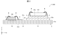
- FIG. FIG. 2 is a schematic cross-sectional view taken along line II-II in FIG. 1
- 1 is a schematic cross-sectional plan view showing an electronic module according to a first embodiment
- FIG. FIG. 4 is a schematic cross-sectional view taken along line IV-IV in FIG. 3
- FIG. 4 is a schematic plan view showing another aspect of the electronic device according to the first embodiment
- FIG. 6 is a schematic cross-sectional view taken along line VI-VI in FIG. 5
- FIG. 4 is a schematic plan view showing another aspect of the electronic device according to the first embodiment
- FIG. 4 is a schematic cross-sectional view showing another aspect of the electronic device according to the first embodiment
- FIG. 4 is a schematic cross-sectional view showing another aspect of the electronic device according to the first embodiment
- FIG. 4 is a schematic cross-sectional view showing another aspect of the electronic device according to the first embodiment
- FIG. 4 is a schematic cross-sectional view showing another aspect of the electronic device according to the first embodiment;
- FIG. 4 is a schematic plan view showing another aspect of the electronic device according to the first embodiment;
- FIG. 11 is a schematic cross-sectional view taken along line XI-XI in FIG. 10;
- FIG. 4 is a schematic plan view showing another aspect of the electronic module according to the first embodiment;
- FIG. 13 is a schematic cross-sectional view taken along line XIII-XIII in FIG. 12;
- FIG. 4 is a schematic plan view showing another aspect of the electronic module according to the first embodiment;
- FIG. 15 is a schematic cross-sectional view taken along line XV-XV in FIG. 14;
- FIG. 4 is a schematic plan view showing another aspect of the electronic module according to the first embodiment;
- FIG. 11 is a schematic cross-sectional view taken along line XI-XI in FIG. 10;
- FIG. 4 is a schematic plan view showing another aspect of the electronic module according to the
- FIG. 17 is a schematic cross-sectional view along line XVII-XVII in FIG. 16;
- FIG. 5 is a schematic plan view showing an electronic device according to a second embodiment;
- FIG. 19 is a schematic cross-sectional view along line XIX-XIX in FIG. 18;
- FIG. 11 is a schematic plan view showing an electronic device according to a third embodiment;
- FIG. 21 is a schematic cross-sectional view along line XXI-XXI in FIG. 20;
- FIG. 11 is a schematic cross-sectional plan view showing an electronic device according to another aspect of the fourth embodiment;
- FIG. 23 is a schematic cross-sectional view taken along line XXIII-XXIII in FIG. 22;
- the heat generated from the light-emitting element propagates to the light-receiving element, the heat may cause problems such as noise or malfunction in the light-receiving element. In other words, heat generated from the light emitting element may cause problems in the electronic device. Therefore, it is desired to reduce the heat that propagates from a heat-generating electronic element to other electronic elements.
- the electronic element mounting board of the present disclosure and the electronic device and electronic module including the board, can reduce the possibility of malfunction due to heat generated by the electronic element.
- each drawing referred to below shows only the constituent elements necessary for explaining the embodiment in a simplified manner. Therefore, the electronic element mounting board, the electronic device, and the electronic module according to the embodiments can include arbitrary components that are not shown in the referenced figures.
- the dimensions of the constituent elements in each drawing may not represent the actual dimensions of the constituent elements, the dimensional ratios of the respective members, and the like faithfully.
- the directions of the electronic element mounting board, the electronic device, and the electronic module are defined using an orthogonal coordinate system XYZ for convenience.
- the positive side in the X-axis direction is the right side
- the positive side in the Y-axis direction is the front side
- the positive side in the Z-axis direction is the upper side.
- the term “annular” includes a rectangular ring, a circular ring, and an elliptical ring.
- the description of "parallel” does not require strict parallelism as long as it is parallel at a visible level.
- FIG. 1 is a schematic plan view showing an electronic device 100 according to the first embodiment.
- FIG. 2 is a schematic cross-sectional view along line II-II in FIG.
- FIG. 3 is a schematic cross-sectional plan view showing the electronic module 200 according to the first embodiment.
- FIG. 4 is a schematic cross-sectional view taken along line IV-IV in FIG.
- the electronic device 100 includes an electronic element mounting board 1 and a light receiving element 110 as a first electronic element mounted on the electronic element mounting board 1. and a light emitting element 120 as a second electronic element mounted on the electronic element mounting board 1 .
- the electronic element mounting substrate 1 includes a base 2, and the shape of the base 2 in plan view is, for example, a rectangular shape.
- the substrate 2 is made of insulating ceramics such as sintered aluminum oxide (alumina ceramics), sintered aluminum nitride, sintered mullite, or sintered glass ceramics.
- the longitudinal direction of the base 2 may be the left-right direction (X-axis direction), and the short-side direction of the base 2 may be the front-rear direction (Y-axis direction).
- the base 2 is made of insulating ceramics, the heat dissipation of the base 2 is high and the rigidity of the base 2 is high. Also, even if the base body 2 has an irregular shape or a through hole is provided in the base body 2, dust such as dust is less likely to be generated. Even when the substrate 2 is heated by the heat generated by the light emitting element 120, it is difficult to generate moisture, gas, and the like. Furthermore, the difference between the thermal expansion coefficient of silicon and the thermal expansion coefficient of the insulating ceramics constituting the light receiving element 110 and the light emitting element 120 is smaller than the difference between the thermal expansion coefficient of the organic material and the thermal expansion coefficient of the insulating ceramics. . Therefore, even when the light emitting element 120 generates heat, the substrate 2 made of insulating ceramics can reduce the stress applied to the electronic elements, compared to the case where the substrate 2 is made of an organic material. .
- the base 2 may have a base 21, and the plan view shape of the base 21 is, for example, a rectangular shape.
- the base 21 has an upper surface 21u and a lower surface 21d.
- the base 21 may be composed of three laminated insulating layers 21a.
- the base 21 may be composed of a plurality of laminated insulating layers 21a other than three, or one insulating layer 21a.
- the base 2 may have a first pedestal 22 positioned on the right side of the upper surface 21 u of the base 21 .
- the first pedestal 22 is integrated with the base 21 and has a first upper surface 22u.
- the first pedestal 22 may be composed of two laminated insulating layers 22a.
- the plurality of insulating layers 22a may have a stepped shape in a cross-sectional view.
- the first pedestal 22 may be composed of a plurality of laminated insulating layers 22a other than two, or one insulating layer 22a.
- a first element mounting area F1 for mounting the light receiving element 110 as the first electronic element may be located on the top surface of the upper insulating layer 22a, which is the first top surface 22u of the first pedestal 22, a first element mounting area F1 for mounting the light receiving element 110 as the first electronic element may be located.
- the first upper surface 22u of the first pedestal 22 includes the first element mounting area F1.
- the base 2 may have the first element mounting area F1 on the first upper surface 22u of the first pedestal 22 .
- the first element mounting area F1 may be an area overlapping with the light receiving element 110 in plan view.
- the first element mounting area F1 may be an area surrounded by imaginary lines connecting alignment marks used when the light receiving element 110 is mounted.
- the first element mounting area F1 may be an area where a metallized layer for mounting the light receiving element 110 is located.
- a second element mounting area F2 for mounting the light emitting element 120 as the second electronic element may be located on the left side of the first pedestal 22 on the upper surface 21u of the base portion 21 .
- the upper surface 21u of the base 21 may include the second element mounting area F2.
- the base 2 may have the second element mounting area F2 on the left side of the first pedestal 22 on the top surface of the base 21 .
- the second element mounting area F2 may be an area overlapping with the light emitting element 120 in plan view.
- the second element mounting area F2 may be an area surrounded by imaginary lines connecting alignment marks used when the light emitting element 120 is mounted.
- the second device mounting region F2 may be a region where a metallized layer for mounting the light emitting device 120 is located.
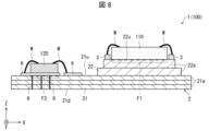
- the first element mounting area F1 and the second element mounting area F2 are parallel and different in height when viewed in cross section. Since the first element mounting area F1 and the second element mounting area F2 are parallel in a cross-sectional view, the mounting process of the light receiving element 110 and the light emitting element 120 is simplified, and the same manufacturing apparatus is used for light reception. Mounting of the element 110 and the light emitting element 120 becomes possible. Moreover, since the mounting surfaces are parallel, it is possible to reduce the possibility that the light receiving element 110 and the light emitting element 120 will come off or shift from the upper surface of the base 2 when the electronic device 100 is used for a long period of time. In addition, the heat generated by the heat generated by the electronic elements can be easily and uniformly transferred from the upper surface of the substrate 2 to directly below.
- the difference in the amount of heat propagation (heat distribution) between the first element mounting area F1 and the second element mounting area F2 can be reduced, thereby facilitating temperature control.
- the light emitted from the light emitting element 120 side can be reflected and directly received by the light receiving element 110 side.
- the first element mounting area F1 may be higher than the second element mounting area F2 by the thickness of the first pedestal 22 in a cross-sectional view.
- the arrangement direction which is the direction in which the first element mounting area F1 and the second element mounting area F2 are arranged, may be the longitudinal direction (X-axis direction) of the base 2 .
- the direction orthogonal to the arrangement direction of the first element mounting area F1 and the second element mounting area F2 may be the lateral direction (Y-axis direction) of the base 2 .
- the arrangement direction is not limited to the X-axis direction of the base 2, depending on the plan view shapes of the base 2, the first element mounting area F1, and the second element mounting area F2.
- the arrangement direction may be, for example, a direction along a line connecting the center of the first element mounting area F1 and the center of the second element mounting area F2.
- a plurality of first connection pads 3 may be provided on the first upper surface 22u of the first pedestal 22 outside the first element mounting region F1.
- Each of the plurality of first connection pads 3 may be connected by a wire W to a corresponding electrode of the light receiving element 110 as the first electronic element.
- each of the plurality of first connection pads 3 may be connected to the corresponding electrode of the light receiving element 110 by wire bonding.
- each of the plurality of first connection pads 3 may be connected to a corresponding electrode of the light receiving element 110 by flip-chip bonding.
- a plurality of first external electrodes 4 may be provided on the lower surface 21 d or the side surface of the base portion 21 . Each of the plurality of first external electrodes 4 may be electrically connected to a corresponding first electrode of the external substrate.
- a plurality of first wiring conductors 5 may be provided inside the base 2 , and the plurality of first wiring conductors 5 connect each of the plurality of first connection pads 3 to the corresponding first external electrode 4 . It may be electrically connected.
- Each of the plurality of first wiring conductors 5 may include a through conductor that penetrates the insulating layer 21a, a through conductor that penetrates the insulating layer 22a, and an internal wiring.
- Two second connection pads 6 may be provided on the upper surface 21 u of the base 21 .
- One of the second connection pads 6 may be located in a region including the second device mounting region F2 on the upper surface 21u of the base 21, and functions as a mounting pad for mounting the light emitting device 120 as the second electronic device. may have The other second connection pad 6 may be located outside the second element mounting region F2 on the upper surface 21u of the base 21.
- Each of the two second connection pads 6 may be connected by a wire W to a corresponding electrode of the light emitting element 120 as the second electronic element.
- each of the two second connection pads 6 may be connected to the corresponding electrode of the light emitting element 120 by wire bonding.
- Each of the two second connection pads 6 may be connected to a corresponding electrode of the light emitting element 120 by flip chip bonding.
- Two second external electrodes 7 may be provided on the lower surface 21 d or the side surface of the base portion 21 . Each of the two second external electrodes 7 may be electrically connected to a corresponding second electrode on the external substrate. Also, two second wiring conductors 8 may be provided inside the base 2 , and the two second wiring conductors 8 connect each of the two second connection pads 6 to the corresponding second external electrode 7 . It may be electrically connected. Each of the plurality of second wiring conductors 8 may include a penetrating conductor penetrating through the insulating layer 21a and an internal wiring.
- the first connection pads 3, the first external electrodes 4, the first wiring conductors 5, the second connection pads 6, the second external electrodes 7, and the second wiring conductors 8 are made of, for example, tungsten (W), molybdenum (Mo), It consists of metal powder metallization containing manganese (Mn), silver (Ag), copper (Cu), or the like as a component.
- the base 2 when the base 2 is made of, for example, an aluminum oxide sintered body, the base 2 is produced as follows. Raw material powders such as aluminum oxide and silicon oxide are mixed with an appropriate organic binder and solvent to produce a slurry. Ceramic green sheets for the insulating layers 21a and 22a are produced by molding this slurry into sheets by a doctor blade method, a calender roll method, or the like. After that, a laminate for the substrate 2 is manufactured by laminating a plurality of ceramic green sheets for the insulating layers 21a and 22a. The substrate 2 is produced by firing the laminate for the substrate 2 at a high temperature (approximately 1300-1600° C.).
- the internal wiring of the first connection pad 3, the first external electrode 4, the first wiring conductor 5, the second connection pad 6, the second external electrode 7, and the second wiring conductor 8 are formed as follows. be.
- the internal wiring is formed by printing a metal paste prepared by mixing tungsten powder with an organic solvent and an organic binder at predetermined positions of the ceramic green sheets for the insulating layers 21a and 22a by a method such as screen printing. It is formed by firing the laminate for 2.
- the penetrating conductors of the first wiring conductor 5 and the penetrating conductors of the second wiring conductor 8 are formed by providing through-conductor holes at predetermined positions in the ceramic green sheets for the insulating layers 21a and 22a, and applying a metal paste to the through-conductor holes. It is formed by filling the
- the surfaces of the first connection pads 3, the first external electrodes 4, the first wiring conductors 5, the second connection pads 6, the second external electrodes 7, and the second wiring conductors 8 exposed to the outside are metallized by plating.
- a nickel plating layer/gold plating layer may be applied as the plating layer.
- the plating method is, for example, an electrolytic plating method or an electroless plating method. This can effectively reduce corrosion of the first wiring conductor 5, the second wiring conductor 8, and the like.
- the metal plating layer is not limited to nickel plating layer/gold plating layer, and may be other metal plating layers including nickel plating layer/palladium plating layer/gold plating layer and the like.
- the first device mounting region F1 and the second device mounting region F2 have different heights when viewed in cross section. is located.
- the first upper surface 22u of the first pedestal 22 includes the first element mounting area F1 and the upper surface of the base portion 21 includes the second element mounting area F2
- the first element mounting area F1 and the second element mounting area F2 is positioned at a different height by the height of the first pedestal 22 in cross-sectional view. This makes it possible to increase the distance between the first element mounting area F1 and the second element mounting area F2.
- the distance from the second element mounting region F2, which is a heat generating portion, to the bottom surface of the base 2 that is in contact with the outside is shorter than the distance from the first element mounting region F1 to the bottom surface, the heat from the heat generating portion is transferred to the base. 2 is easily propagated to the outside. Therefore, the heat generated by the light emitting element 120 as the second electronic element is less likely to propagate to the light receiving element 110 as the first electronic element. Therefore, it is possible to reduce the possibility of malfunction of the light receiving element 110 due to the heat generated by the light emitting element 120 .
- the first element mounting area F1 and the second element mounting area F2 in a plan view are increased.
- the distance to the element mounting area F2 can be shortened. That is, it is possible to reduce the size of the electronic device 100 .
- the difference in height between the first element mounting region F1 and the second element mounting region F2 in a cross-sectional view can be reduced by the plurality of insulating layers 22a. It becomes easy to set large. Moreover, it becomes easier to adjust the height of the first pedestal 22 . Therefore, the heat generated by the light emitting element 120 is more difficult to propagate to the light receiving element 110 side. This can further reduce the possibility that the light-receiving element 110 will malfunction due to the heat generated by the light-emitting element 120 .
- the installation position of the first connection pad 3 can be adjusted.
- an electronic component such as a capacitor can be installed on the upper surface of the lower insulating layer 22a.
- the first connection pads 3 and electronic components can be placed close to each other, the electrical characteristics of the electronic device 100 are improved.
- the electronic device 100 includes an electronic element mounting substrate 1, a light receiving element 110 as a first electronic element mounted in a first element mounting region F1 of a base 2, and a base and a light emitting element 120 as a second electronic element mounted in the second element mounting region F2.
- a first electronic element other than the light receiving element 110 may be mounted on the first element mounting area F1 of the base 2 .
- a second electronic element other than the light emitting element 120 may be mounted on the second element mounting area F2 of the base 2 .
- the light receiving element 110 is, for example, a photodiode, and may be bonded to the first element mounting area F1 of the base 2 with an adhesive. Each of the plurality of electrodes of the light receiving element 110 may be connected to the corresponding first connection pad 3 by wire bonding or flip chip bonding.
- the light emitting element 120 is, for example, an LED (Light Emitting Diode) or a VCSEL (Vertical Cavity Surface Emitting Laser) type laser diode, and is joined to the second element mounting region F2 of the base 2 by one of the second connection pads 6. good too.
- Each of the two electrodes of the light emitting element 120 may be connected to the corresponding second connection pad 6 by wire bonding or flip chip bonding.
- the electronic device 100 includes the electronic element mounting substrate 1, so that the heat generated by the light emitting element 120 propagates to the light receiving element 110, causing the light receiving element 110 to deteriorate. It is possible to further reduce the possibility of occurrence of troubles such as noise or malfunction.
- the electronic module 200 includes an electronic device 100 and a housing 210 positioned on the upper surface 21u of the base 21 of the base 2 of the electronic device 100.
- the housing 210 is made of, for example, metal such as aluminum (Al) or resin such as PBT (polybutylene terephthalate).
- the housing 210 may be bonded to the upper surface 21u of the base 21 of the base 2 with a bonding material such as brazing material or adhesive.
- the housing 210 may cover the top of the first element mounting area F1 of the base 2 .
- the housing 210 may cover the second element mounting area F2 of the base 2 instead of covering the first element mounting area F1 of the base 2 .
- the housing 210 may have a holding hole 220 in its upper portion, and the holding hole 220 passes through the upper portion of the housing 210 .
- a lens 230 may be provided in the holding hole 220 of the housing 210 , and the lens 230 may have a function of converging external light entering from the outside onto the light receiving surface of the light receiving element 110 .
- An IR cut filter that blocks infrared rays may be provided on the light exit side of the lens 230 .
- the electronic module 200 includes the electronic device 100. Therefore, noise is generated in the light receiving element 110 due to the heat generated in the light emitting element 120 propagating to the light receiving element 110 side. Alternatively, it is possible to further reduce the possibility of occurrence of troubles such as malfunction.
- FIG. 5 is a schematic plan view showing another aspect of the electronic device 100 according to the first embodiment.
- FIG. 6 is a schematic cross-sectional view taken along line VI-VI in FIG.
- FIG. 7 is a schematic plan view showing another aspect of the electronic device 100 according to the first embodiment.
- FIG. 8 is a schematic cross-sectional view showing another aspect of the electronic device 100 according to the first embodiment.
- FIG. 9 is a schematic cross-sectional view showing another aspect of the electronic device 100 according to the first embodiment.
- FIG. 10 is a schematic plan view showing another aspect of the electronic device 100 according to the first embodiment.
- 11 is a schematic cross-sectional view along line XI-XI in FIG. 10.
- each side surface of the plurality of insulating layers 22a may match when viewed from above.
- the size and weight of the substrate 2 can be reduced, in other words, the size and weight of the electronic element mounting board 1 can be reduced. That is, in the contents of the present disclosure, instead of lengthening the planar direction propagation path between the light emitting element 120 and the light receiving element 110 to reduce heat propagation, the thickness direction propagation path is lengthened. , the electronic element mounting board 1 can be miniaturized. Matching the side surfaces of the insulating layer 22a in plan view is advantageous for further miniaturization of the electronic element mounting substrate 1. As shown in FIG.
- the two first side surfaces 22s of the first pedestal 22 parallel to the left-right direction (X-axis direction), which is the arrangement direction of the first element mounting area F1 and the second element mounting area F2, are In plan view, it may correspond to the two third side surfaces 21s of the base portion 21 parallel to the left-right direction.
- the first upper surface 22u of the first pedestal 22 expands in the front-rear direction (Y-axis direction).
- an electronic component such as a capacitor can be installed at the same height as the light receiving element 110 as the first electronic element, so that the electrical characteristics of the electronic device 100 are improved.
- the electronic element mounting substrate 1 may include a plurality of thermal vias 9 penetrating along the thickness direction of the base 2 at positions overlapping the light emitting elements 120 in top view. Also, each of the plurality of thermal vias 9 may be connected to the second element mounting region F2.
- the thermal via 9 is made of metal powder metallization containing, for example, tungsten (W), molybdenum (Mo), manganese (Mn), silver (Ag), copper (Cu), or the like.
- the thermal vias 9 are formed by providing thermal via holes at predetermined positions in the ceramic green sheets for the insulating layers 21a and 22a and filling the thermal via holes with a metal paste.
- the heat generated by the light emitting elements 120 propagates to the bottom surface of the base 2 . This can further reduce the possibility that the light-receiving element 110 will malfunction due to the heat generated by the light-emitting element 120 .
- the electronic device mounting substrate 1 may include a heat sink 10 positioned on the lower surface 21d of the base portion 21, which is the lower surface of the base 2, and dissipating heat generated from the light emitting elements 120.
- the heat sink 10 may be bonded to the lower surface 21d of the base 21 with a bonding material such as a resin adhesive.
- the heat sink 10 may be made of, for example, a highly thermally conductive metal such as aluminum.
- the heat generated by the light emitting device 120 is dissipated by the heat sink 10. This can further reduce the possibility that the light-receiving element 110 will malfunction due to the heat generated by the light-emitting element 120 .
- the heat shield part 11 is made of, for example, thermosetting resin or thermoplastic resin.
- the grooves 21g of the base 21 are formed by subjecting the ceramic green sheets for the insulating layer to suitable punching or the like before firing the laminate for the base 2 .
- the heat generated by the light emitting element 120 is more difficult to propagate to the light receiving element 110 side. This can further reduce the possibility that the light-receiving element 110 will malfunction due to the heat generated by the light-emitting element 120 .
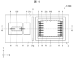
- FIG. 12 is a schematic plan view showing another aspect of the electronic module 200 according to the first embodiment.
- 13 is a schematic cross-sectional view along line XIII-XIII in FIG. 12.
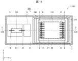
- FIG. 14 is a schematic plan view showing another aspect of the electronic module 200 according to the first embodiment.
- 15 is a schematic cross-sectional view along line XV-XV in FIG. 14.
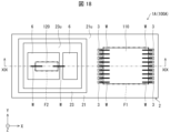
- FIG. 16 is a schematic plan view showing another aspect of the electronic module 200 according to the first embodiment. 17 is a schematic cross-sectional view along line XVII-XVII in FIG. 16.
- a portion of the portion of the housing 210 that joins the base 2 may be located on the upper surface of the insulating layer 22a on the lower layer side of the first pedestal 22 of the base 2.
- the front view shape of the housing 210 may be an inverted U shape.
- the housing 210 may be bonded to the upper surface of the insulating layer 22a on the lower layer side of the first pedestal 22 of the base 2 with a bonding material such as brazing material or adhesive.
- the side view shape of the housing 210 may be an inverted U shape.
- the electronic module 200 includes a housing 210 as a first housing located on the upper surface 21 u of the base 21 of the base 2 , and a housing 210 on the upper surface 21 u of the base 21 of the base 2 .
- a second housing 240 may be located.
- the second housing 240 is made of, for example, metal such as aluminum (Al) or resin such as PBT (polybutylene terephthalate).
- the second housing 240 may be bonded to the upper surface 21u of the base 21 of the base 2 with a bonding material such as brazing material or adhesive.
- the second housing 240 may cover above the first element mounting area F1 of the base 2, above the second element mounting area F2 of the base 2, and above the first housing 210.
- the second housing 240 may have two holding holes 250 , 260 in its upper portion, each of the two holding holes 250 , 260 passing through the upper portion of the second housing 240 .
- a lens 270 , 280 may be provided in each of the two holding holes 250 , 260 of the second housing 240 .
- Lens 270 may have the function of converging, diverging, or collimating the emitted light emitted from light emitting element 120 .
- the lens 270 may have a function of converging external light incident from the outside.
- each of the two holding holes 250 and 260 of the second housing 240 may be provided with a member capable of transmitting light, such as a glass plate.
- FIG. 18 is a schematic plan view showing an electronic device 100A according to the second embodiment.
- 19 is a schematic cross-sectional view taken along line XIX-XIX in FIG. 18.
- the electronic device 100A includes an electronic element mounting substrate 1A, a light receiving element 110 as a first electronic element mounted on the electronic element mounting substrate 1A, and an electronic element mounting substrate. and a light emitting element 120 as a second electronic element mounted on 1A.
- An electronic device mounting substrate 1A according to the second embodiment has the same structure as the electronic device mounting substrate 1 according to the first embodiment except for a part.
- the points that differ from the configuration of the electronic device mounting substrate 1 according to the first embodiment will be described.
- members having the same functions as the members explained in the first embodiment are denoted by the same reference numerals.
- the base 2 may have a second pedestal 23 located on the left side of the upper surface of the base 21.
- the second pedestal 23 is integrated with the base 21 and has a second upper surface 23u.
- the second pedestal 23 may be composed of two laminated insulating layers 23a.
- the plurality of insulating layers 23a may have a stepped shape in a cross-sectional view.
- the second pedestal 23 may be composed of a plurality of laminated insulating layers 23a other than two, or one insulating layer 23a.
- a first element mounting area F1 for mounting the light receiving element 110 as the first electronic element may be positioned on the right side of the upper surface 21u of the base portion 21 .
- the base 2 may have the first element mounting area F1 on the right side of the upper surface 21u of the base 21 .
- a second element mounting area F2 for mounting the light emitting element 120 as the second electronic element may be located on the top surface of the upper insulating layer 23a, which is the second top surface 23u of the second pedestal 23.
- the second upper surface 23u of the second pedestal 23 includes the second element mounting area F2.
- the base 2 may have the second element mounting area F2 on the second upper surface 23u of the second pedestal 23 .
- first element mounting area F1 and the second element mounting area F2 are parallel to each other and have different heights when viewed in cross section.
- the second element mounting area F2 may be higher than the first element mounting area F1 by the thickness of the second pedestal 23 in a cross-sectional view.
- the base 2 having the second pedestal 23 is manufactured by the same method as the base 2 having the first pedestal 22 .
- the first element mounting area F1 and the second element mounting area F2 are different heights in a cross-sectional view. is located. This makes it possible to increase the distance between the first element mounting area F1 and the second element mounting area F2. Also, the distance from the first element mounting area F1 to the bottom surface of the substrate 2 that is in contact with the outside is shorter than the distance from the second element mounting area F2 to the bottom surface. When the heat from the light emitting element 120 is propagated, at least part of the heat is dissipated to the outside in contact with the base 2, so that the influence of the heat on the light receiving element 110 can be reduced.
- the heat generated by the light emitting element 120 as the second electronic element is less likely to propagate to the light receiving element 110 as the first electronic element.
- the possibility of malfunction of the light receiving element 110 due to heat generated by the light emitting element 120 can be reduced.
- the distance between the first element mounting area F1 and the second element mounting area F2 is increased by increasing the distance between the first element mounting area F1 and the second element mounting area F2 in cross-sectional view. By providing it, it is possible to reduce the size of the electronic device 100A.
- the plurality of insulating layers 23a can reduce the difference in height between the first element mounting area F1 and the second element mounting area F2 in a cross-sectional view. It becomes easy to set large. Also, it becomes easier to adjust the height of the second pedestal 23 . Therefore, the heat generated by the light emitting element 120 is more difficult to propagate to the light receiving element 110 side. This can further reduce the possibility that the light-receiving element 110 will malfunction due to the heat generated by the light-emitting element 120 .
- the installation position of the second connection pad 6 can be adjusted.
- an electronic component such as a capacitor can be installed on the upper surface of the lower insulating layer 23a in addition to the upper surface of the uppermost insulating layer 23a.
- the second connection pads 6 and electronic components can be placed close to each other, the electrical characteristics of the electronic device 100A are improved.
- Each side surface of the plurality of insulating layers 23a may be aligned in plan view.
- the two second side surfaces of the second pedestal 23 parallel to the left-right direction (X-axis direction) in which the first element mounting area F1 and the second element mounting area F2 are arranged are base portions parallel to the left-right direction in plan view. 21 may coincide with the two third sides 21s.
- the second upper surface 23u of the second pedestal 23 expands in the front-rear direction (Y-axis direction). Thereby, a space for installing the housing 210 on the second upper surface 23u of the second pedestal 23 can be secured.
- an electronic component such as a capacitor can be installed at the same height as the light emitting element 120 as the second electronic element, thereby improving the electrical characteristics of the electronic device 100A.
- the base 2 may have a first pedestal 22 positioned on the right side of the upper surface 21u of the base 21 .
- the first element mounting region F1 may be located on the top surface of the upper insulating layer 22a, which is the first top surface 22u of the first pedestal 22. As shown in FIG.
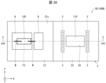
- FIG. 20 is a schematic plan view showing an electronic device 100B according to the third embodiment.
- FIG. 21 is a schematic cross-sectional view taken along line XXI-XXI in FIG. 20, and FIG. 21 shows only a cross-sectional view of the electronic device 100B according to the third embodiment.
- the electronic device 100B includes an electronic element mounting board 1B, a light receiving element 110 as a first electronic element mounted on the electronic element mounting board 1B, and an electronic element mounting board 1B. and a light emitting element 120 as a second electronic element mounted on the substrate 1B.
- An electronic device mounting substrate 1B according to the third embodiment has the same structure as the electronic device mounting substrate 1 according to the first embodiment except for a part.
- the points that differ from the configuration of the electronic device mounting substrate 1 according to the first embodiment will be described.
- members having the same functions as the members explained in the first embodiment are denoted by the same reference numerals.
- the base 2 may have a stepped first housing hole 24 for housing the light receiving element 110 .
- the first receiving hole 24 may penetrate in the thickness direction of the base 2 from the upper surface of the first pedestal 22 to the lower surface of the base portion 21 .
- the plan view shape of the first accommodation hole 24 may be rectangular.
- a first element mounting area F1 for mounting the light receiving element 110 as the first electronic element may be positioned on the stepped surface 24p of the first housing hole 24 having a rectangular ring shape.
- the base body 2 may have the first element mounting area F1 on the step surface 24p of the first receiving hole 24 .
- the first element mounting region F1 may be a region that overlaps the step surface 24p of the first receiving hole 24 in plan view.
- the first element mounting area F1 may be an area surrounded by imaginary lines connecting alignment marks used when the light receiving element 110 is mounted.
- the first element mounting area F1 may be an area where a metallized layer for mounting the light receiving element 110 is located.
- the first element mounting area F1 and the second element mounting area F2 are parallel to each other and have different heights in a cross-sectional view.
- a plurality of first connection pads 3 may be provided on the stepped surface 24p of the first accommodation hole 24 .
- Each of the plurality of first connection pads 3 may be connected by a bump B to a corresponding electrode of the light emitting element 120 as the second electronic element.
- each of the plurality of first connection pads 3 may be connected to the corresponding electrode of the light receiving element 110 by flip chip bonding.
- Each of the plurality of first connection pads 3 may be connected to a corresponding electrode of the light receiving element 110 by wire bonding.
- the step surface 24p is a part of the surface of the insulating layer 22a located above the first receiving hole 24. As shown in FIG.
- the first receiving hole 24 of the base 2 is formed by performing appropriate punching or the like on the ceramic green sheets for the insulating layers 21a and 22a before firing the laminate for the base 2.
- the first element mounting area F1 and the second element mounting area F2 are different heights in a cross-sectional view. is located. This makes it possible to increase the distance between the first element mounting area F1 and the second element mounting area F2.
- the distance from the second element mounting region F2, which is a heat generating portion, to the bottom surface of the base 2 that is in contact with the outside is shorter than the distance from the first element mounting region F1 to the bottom surface, the heat from the heat generating portion is transferred to the base. 2 is easily propagated to the outside.
- the heat generated by the light emitting element 120 as the second electronic element is less likely to propagate to the light receiving element 110 as the first electronic element. Therefore, it is possible to reduce the possibility of malfunction of the light receiving element 110 due to the heat generated by the light emitting element 120 .
- the contact area between the light receiving element 110 and the base 21 via the bumps B becomes small, and the light emitting element 120 It becomes difficult for the heat generated in to propagate to the light receiving element 110 side. This can further reduce the possibility that the light-receiving element 110 will malfunction due to the heat generated by the light-emitting element 120 .
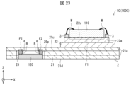
- FIG. 22 is a schematic cross-sectional plan view showing an electronic device 100C according to another aspect of the fourth embodiment.
- FIG. 23 is a schematic cross-sectional view taken along line XXIII-XXIII in FIG. 22, and FIG. 23 shows only a cross-sectional view of an electronic device 100C according to another aspect of the fourth embodiment.
- the electronic device 100C includes an electronic element mounting board 1C, a light receiving element 110 as a first electronic element mounted on the electronic element mounting board 1C, and an electronic element mounting board 1C. and a light emitting element 120 as a second electronic element mounted on the substrate 1C.
- An electronic device mounting substrate 1C according to the fourth embodiment has the same structure as the electronic device mounting substrate 1 according to the first embodiment except for a part.
- the points different from the configuration of the electronic device mounting substrate 1 according to the first embodiment will be described.
- members having the same functions as the members explained in the first embodiment are denoted by the same reference numerals.
- the base 2 may have a stepped second housing hole 25 for housing the light emitting element 120 .
- the second receiving hole 25 may penetrate in the thickness direction of the base 2 from the upper surface of the base portion 21 to the lower surface of the base portion 21 .
- the plan view shape of the second accommodation hole 25 may be rectangular.
- a second element mounting area F2 for mounting the light emitting element 120 as the second electronic element may be located on the stepped surface 25p of the second housing hole 25 having a rectangular shape.
- the base 2 may have the second element mounting region F2 on the stepped surface 25p of the second housing hole 25 .
- the second element mounting area F2 may be an area that overlaps the step surface 25p of the second housing hole 25 in plan view.
- the second element mounting area F2 may be an area surrounded by imaginary lines connecting alignment marks used when the light emitting element 120 is mounted.
- the second device mounting region F2 may be a region where a metallized layer for mounting the light emitting device 120 is located.
- the first element mounting area F1 and the second element mounting area F2 are parallel to each other and have different heights in a cross-sectional view.
- a plurality of second connection pads 6 may be provided on the stepped surface 25p of the second accommodation hole 25 .
- Each of the plurality of second connection pads 6 may be connected by a bump B to a corresponding electrode of the light emitting element 120 .
- each of the plurality of second connection pads 6 may be connected to the corresponding electrode of the light emitting element 120 by flip chip bonding.
- Each of the plurality of second connection pads 6 may be connected to a corresponding electrode of the light emitting element 120 by wire bonding.
- the step surface 25p is a part of the surface of the insulating layer 21a located above the second receiving hole 25. As shown in FIG.
- the second housing hole 25 of the base 2 is formed by subjecting the ceramic green sheet for the insulating layer 21a to suitable punching or the like before firing the laminate for the base 2 .
- the first element mounting area F1 and the second element mounting area F2 have different heights when viewed in cross section. is located. This makes it possible to increase the distance between the first element mounting area F1 and the second element mounting area F2. Therefore, the heat generated by the light emitting element 120 as the second electronic element is less likely to propagate to the light receiving element 110 as the first electronic element. Therefore, it is possible to reduce the possibility of malfunction of the light receiving element 110 due to the heat generated by the light emitting element 120 .
- the contact area between the light emitting element 120 and the base 21 via the bumps B becomes small, and the light emitting element 120 It becomes difficult for the heat generated in to propagate to the light receiving element 110 side. This can further reduce the possibility that the light-receiving element 110 will malfunction due to the heat generated by the light-emitting element 120 . Furthermore, the fact that the light emitting element 120 is accommodated in the second accommodation hole 25 is advantageous in terms of reducing the height of the electronic device 100C.
Landscapes
- Structures For Mounting Electric Components On Printed Circuit Boards (AREA)
- Cooling Or The Like Of Semiconductors Or Solid State Devices (AREA)
- Led Device Packages (AREA)
Priority Applications (3)
| Application Number | Priority Date | Filing Date | Title |
|---|---|---|---|
| JP2023556280A JP7753380B2 (ja) | 2021-10-25 | 2022-10-11 | 電子素子実装用基板、電子装置、および電子モジュール |
| CN202280071217.4A CN118251763A (zh) | 2021-10-25 | 2022-10-11 | 电子元件安装用基板、电子装置以及电子模块 |
| EP22886672.9A EP4425546A1 (en) | 2021-10-25 | 2022-10-11 | Substrate for mounting electronic elements, electronic device, and electronic module |
Applications Claiming Priority (2)
| Application Number | Priority Date | Filing Date | Title |
|---|---|---|---|
| JP2021174038 | 2021-10-25 | ||
| JP2021-174038 | 2021-10-25 |
Publications (1)
| Publication Number | Publication Date |
|---|---|
| WO2023074342A1 true WO2023074342A1 (ja) | 2023-05-04 |
Family
ID=86159291
Family Applications (1)
| Application Number | Title | Priority Date | Filing Date |
|---|---|---|---|
| PCT/JP2022/037801 Ceased WO2023074342A1 (ja) | 2021-10-25 | 2022-10-11 | 電子素子実装用基板、電子装置、および電子モジュール |
Country Status (4)
| Country | Link |
|---|---|
| EP (1) | EP4425546A1 (https=) |
| JP (1) | JP7753380B2 (https=) |
| CN (1) | CN118251763A (https=) |
| WO (1) | WO2023074342A1 (https=) |
Cited By (1)
| Publication number | Priority date | Publication date | Assignee | Title |
|---|---|---|---|---|
| WO2025134746A1 (ja) * | 2023-12-21 | 2025-06-26 | Hoya株式会社 | 光源装置、電子内視鏡システム |
Citations (9)
| Publication number | Priority date | Publication date | Assignee | Title |
|---|---|---|---|---|
| JP2002344008A (ja) * | 2001-05-17 | 2002-11-29 | Fuji Xerox Co Ltd | 光素子モジュール |
| JP2005101366A (ja) * | 2003-09-25 | 2005-04-14 | Kyocera Corp | 高周波モジュール |
| JP2014107460A (ja) * | 2012-11-29 | 2014-06-09 | Kyocera Corp | 配線基板およびそれを用いた実装構造体 |
| JP2016535533A (ja) * | 2013-08-26 | 2016-11-10 | オプティツ インコーポレイテッド | 一体型カメラモジュール及びその製造方法 |
| JP2017198950A (ja) * | 2016-04-28 | 2017-11-02 | APRESIA Systems株式会社 | 光通信モジュール |
| JP2018110262A (ja) * | 2016-08-10 | 2018-07-12 | 京セラ株式会社 | 電気素子搭載用パッケージ、アレイ型パッケージおよび電気装置 |
| JP2020155622A (ja) | 2019-03-20 | 2020-09-24 | 富士ゼロックス株式会社 | 発光装置、光学装置および情報処理装置 |
| JP2021032603A (ja) * | 2019-08-20 | 2021-03-01 | ソニーセミコンダクタソリューションズ株式会社 | 測距装置、電子機器、および、測距装置の製造方法 |
| JP2021130917A (ja) * | 2020-02-18 | 2021-09-09 | 株式会社Lixil | 給水装置 |
-
2022
- 2022-10-11 CN CN202280071217.4A patent/CN118251763A/zh active Pending
- 2022-10-11 JP JP2023556280A patent/JP7753380B2/ja active Active
- 2022-10-11 EP EP22886672.9A patent/EP4425546A1/en not_active Withdrawn
- 2022-10-11 WO PCT/JP2022/037801 patent/WO2023074342A1/ja not_active Ceased
Patent Citations (9)
| Publication number | Priority date | Publication date | Assignee | Title |
|---|---|---|---|---|
| JP2002344008A (ja) * | 2001-05-17 | 2002-11-29 | Fuji Xerox Co Ltd | 光素子モジュール |
| JP2005101366A (ja) * | 2003-09-25 | 2005-04-14 | Kyocera Corp | 高周波モジュール |
| JP2014107460A (ja) * | 2012-11-29 | 2014-06-09 | Kyocera Corp | 配線基板およびそれを用いた実装構造体 |
| JP2016535533A (ja) * | 2013-08-26 | 2016-11-10 | オプティツ インコーポレイテッド | 一体型カメラモジュール及びその製造方法 |
| JP2017198950A (ja) * | 2016-04-28 | 2017-11-02 | APRESIA Systems株式会社 | 光通信モジュール |
| JP2018110262A (ja) * | 2016-08-10 | 2018-07-12 | 京セラ株式会社 | 電気素子搭載用パッケージ、アレイ型パッケージおよび電気装置 |
| JP2020155622A (ja) | 2019-03-20 | 2020-09-24 | 富士ゼロックス株式会社 | 発光装置、光学装置および情報処理装置 |
| JP2021032603A (ja) * | 2019-08-20 | 2021-03-01 | ソニーセミコンダクタソリューションズ株式会社 | 測距装置、電子機器、および、測距装置の製造方法 |
| JP2021130917A (ja) * | 2020-02-18 | 2021-09-09 | 株式会社Lixil | 給水装置 |
Cited By (1)
| Publication number | Priority date | Publication date | Assignee | Title |
|---|---|---|---|---|
| WO2025134746A1 (ja) * | 2023-12-21 | 2025-06-26 | Hoya株式会社 | 光源装置、電子内視鏡システム |
Also Published As
| Publication number | Publication date |
|---|---|
| JP7753380B2 (ja) | 2025-10-14 |
| EP4425546A1 (en) | 2024-09-04 |
| JPWO2023074342A1 (https=) | 2023-05-04 |
| CN118251763A (zh) | 2024-06-25 |
Similar Documents
| Publication | Publication Date | Title |
|---|---|---|
| TWI605280B (zh) | Electronic module | |
| KR20190034545A (ko) | 전기 소자 탑재용 패키지, 어레이형 패키지, 및 전기 장치 | |
| JPWO2020017582A1 (ja) | モジュール | |
| CN112020771A (zh) | 电子元件安装用基板、电子装置以及电子模块 | |
| CN108461453A (zh) | 电子元件安装用基板、电子装置以及电子模块 | |
| JP7300454B2 (ja) | 配線基板、電子装置および電子モジュール | |
| JP4555026B2 (ja) | 光電変換モジュール、積層基板接合体 | |
| WO2023074342A1 (ja) | 電子素子実装用基板、電子装置、および電子モジュール | |
| KR101543563B1 (ko) | 광전자 반도체 컴포넌트 | |
| JP4975698B2 (ja) | 光電変換モジュール | |
| JP6626735B2 (ja) | 電子部品搭載用基板、電子装置および電子モジュール | |
| JP7587025B2 (ja) | 基板、パッケージ、電子部品および発光装置。 | |
| JP6666200B2 (ja) | 配線基板および電子装置 | |
| JP6940373B2 (ja) | 受光装置 | |
| JP7652908B2 (ja) | 電子素子実装用基板、電子装置および電子モジュール | |
| JP6382615B2 (ja) | 配線基板、電子装置および電子装置の実装構造 | |
| JP6622583B2 (ja) | 配線基板および電子装置 | |
| CN114270499A (zh) | 安装基板以及电子装置 | |
| JP2007227739A (ja) | 電子部品収納用パッケージ及び電子部品装置 | |
| JP7679479B2 (ja) | 配線基板および電子装置 | |
| JP7433766B2 (ja) | 回路基板、電子部品および電子モジュール | |
| JP2004282227A (ja) | 光モジュール及びその製造方法並びに電子機器 | |
| WO2023243271A1 (ja) | 半導体装置 | |
| WO2024181322A1 (ja) | 配線基板および配線基板を用いた光モジュール | |
| JPWO2023026904A5 (https=) |
Legal Events
| Date | Code | Title | Description |
|---|---|---|---|
| 121 | Ep: the epo has been informed by wipo that ep was designated in this application |
Ref document number: 22886672 Country of ref document: EP Kind code of ref document: A1 |
|
| ENP | Entry into the national phase |
Ref document number: 2023556280 Country of ref document: JP Kind code of ref document: A |
|
| WWE | Wipo information: entry into national phase |
Ref document number: 202280071217.4 Country of ref document: CN Ref document number: 18703800 Country of ref document: US |
|
| WWE | Wipo information: entry into national phase |
Ref document number: 2022886672 Country of ref document: EP |
|
| NENP | Non-entry into the national phase |
Ref country code: DE |
|
| ENP | Entry into the national phase |
Ref document number: 2022886672 Country of ref document: EP Effective date: 20240527 |