WO2023073479A1 - 表示装置、及び電子機器 - Google Patents
表示装置、及び電子機器 Download PDFInfo
- Publication number
- WO2023073479A1 WO2023073479A1 PCT/IB2022/059838 IB2022059838W WO2023073479A1 WO 2023073479 A1 WO2023073479 A1 WO 2023073479A1 IB 2022059838 W IB2022059838 W IB 2022059838W WO 2023073479 A1 WO2023073479 A1 WO 2023073479A1
- Authority
- WO
- WIPO (PCT)
- Prior art keywords
- switch
- terminal
- transistor
- display device
- wiring
- Prior art date
- Legal status (The legal status is an assumption and is not a legal conclusion. Google has not performed a legal analysis and makes no representation as to the accuracy of the status listed.)
- Ceased
Links
Images




















































Classifications
-
- G—PHYSICS
- G09—EDUCATION; CRYPTOGRAPHY; DISPLAY; ADVERTISING; SEALS
- G09G—ARRANGEMENTS OR CIRCUITS FOR CONTROL OF INDICATING DEVICES USING STATIC MEANS TO PRESENT VARIABLE INFORMATION
- G09G3/00—Control arrangements or circuits, of interest only in connection with visual indicators other than cathode-ray tubes
- G09G3/20—Control arrangements or circuits, of interest only in connection with visual indicators other than cathode-ray tubes for presentation of an assembly of a number of characters, e.g. a page, by composing the assembly by combination of individual elements arranged in a matrix no fixed position being assigned to or needed to be assigned to the individual characters or partial characters
- G09G3/22—Control arrangements or circuits, of interest only in connection with visual indicators other than cathode-ray tubes for presentation of an assembly of a number of characters, e.g. a page, by composing the assembly by combination of individual elements arranged in a matrix no fixed position being assigned to or needed to be assigned to the individual characters or partial characters using controlled light sources
- G09G3/30—Control arrangements or circuits, of interest only in connection with visual indicators other than cathode-ray tubes for presentation of an assembly of a number of characters, e.g. a page, by composing the assembly by combination of individual elements arranged in a matrix no fixed position being assigned to or needed to be assigned to the individual characters or partial characters using controlled light sources using electroluminescent panels
- G09G3/32—Control arrangements or circuits, of interest only in connection with visual indicators other than cathode-ray tubes for presentation of an assembly of a number of characters, e.g. a page, by composing the assembly by combination of individual elements arranged in a matrix no fixed position being assigned to or needed to be assigned to the individual characters or partial characters using controlled light sources using electroluminescent panels semiconductive, e.g. using light-emitting diodes [LED]
- G09G3/3208—Control arrangements or circuits, of interest only in connection with visual indicators other than cathode-ray tubes for presentation of an assembly of a number of characters, e.g. a page, by composing the assembly by combination of individual elements arranged in a matrix no fixed position being assigned to or needed to be assigned to the individual characters or partial characters using controlled light sources using electroluminescent panels semiconductive, e.g. using light-emitting diodes [LED] organic, e.g. using organic light-emitting diodes [OLED]
- G09G3/3225—Control arrangements or circuits, of interest only in connection with visual indicators other than cathode-ray tubes for presentation of an assembly of a number of characters, e.g. a page, by composing the assembly by combination of individual elements arranged in a matrix no fixed position being assigned to or needed to be assigned to the individual characters or partial characters using controlled light sources using electroluminescent panels semiconductive, e.g. using light-emitting diodes [LED] organic, e.g. using organic light-emitting diodes [OLED] using an active matrix
- G09G3/3233—Control arrangements or circuits, of interest only in connection with visual indicators other than cathode-ray tubes for presentation of an assembly of a number of characters, e.g. a page, by composing the assembly by combination of individual elements arranged in a matrix no fixed position being assigned to or needed to be assigned to the individual characters or partial characters using controlled light sources using electroluminescent panels semiconductive, e.g. using light-emitting diodes [LED] organic, e.g. using organic light-emitting diodes [OLED] using an active matrix with pixel circuitry controlling the current through the light-emitting element
-
- G—PHYSICS
- G09—EDUCATION; CRYPTOGRAPHY; DISPLAY; ADVERTISING; SEALS
- G09F—DISPLAYING; ADVERTISING; SIGNS; LABELS OR NAME-PLATES; SEALS
- G09F9/00—Indicating arrangements for variable information in which the information is built-up on a support by selection or combination of individual elements
- G09F9/30—Indicating arrangements for variable information in which the information is built-up on a support by selection or combination of individual elements in which the desired character or characters are formed by combining individual elements
-
- G—PHYSICS
- G09—EDUCATION; CRYPTOGRAPHY; DISPLAY; ADVERTISING; SEALS
- G09F—DISPLAYING; ADVERTISING; SIGNS; LABELS OR NAME-PLATES; SEALS
- G09F9/00—Indicating arrangements for variable information in which the information is built-up on a support by selection or combination of individual elements
- G09F9/30—Indicating arrangements for variable information in which the information is built-up on a support by selection or combination of individual elements in which the desired character or characters are formed by combining individual elements
- G09F9/33—Indicating arrangements for variable information in which the information is built-up on a support by selection or combination of individual elements in which the desired character or characters are formed by combining individual elements being semiconductor devices, e.g. diodes
- G09F9/335—Indicating arrangements for variable information in which the information is built-up on a support by selection or combination of individual elements in which the desired character or characters are formed by combining individual elements being semiconductor devices, e.g. diodes being organic light emitting diodes [OLED]
-
- G—PHYSICS
- G09—EDUCATION; CRYPTOGRAPHY; DISPLAY; ADVERTISING; SEALS
- G09G—ARRANGEMENTS OR CIRCUITS FOR CONTROL OF INDICATING DEVICES USING STATIC MEANS TO PRESENT VARIABLE INFORMATION
- G09G3/00—Control arrangements or circuits, of interest only in connection with visual indicators other than cathode-ray tubes
- G09G3/20—Control arrangements or circuits, of interest only in connection with visual indicators other than cathode-ray tubes for presentation of an assembly of a number of characters, e.g. a page, by composing the assembly by combination of individual elements arranged in a matrix no fixed position being assigned to or needed to be assigned to the individual characters or partial characters
-
- G—PHYSICS
- G09—EDUCATION; CRYPTOGRAPHY; DISPLAY; ADVERTISING; SEALS
- G09G—ARRANGEMENTS OR CIRCUITS FOR CONTROL OF INDICATING DEVICES USING STATIC MEANS TO PRESENT VARIABLE INFORMATION
- G09G2300/00—Aspects of the constitution of display devices
- G09G2300/04—Structural and physical details of display devices
- G09G2300/0421—Structural details of the set of electrodes
- G09G2300/0426—Layout of electrodes and connections
-
- G—PHYSICS
- G09—EDUCATION; CRYPTOGRAPHY; DISPLAY; ADVERTISING; SEALS
- G09G—ARRANGEMENTS OR CIRCUITS FOR CONTROL OF INDICATING DEVICES USING STATIC MEANS TO PRESENT VARIABLE INFORMATION
- G09G2300/00—Aspects of the constitution of display devices
- G09G2300/08—Active matrix structure, i.e. with use of active elements, inclusive of non-linear two terminal elements, in the pixels together with light emitting or modulating elements
- G09G2300/0809—Several active elements per pixel in active matrix panels
- G09G2300/0842—Several active elements per pixel in active matrix panels forming a memory circuit, e.g. a dynamic memory with one capacitor
-
- G—PHYSICS
- G09—EDUCATION; CRYPTOGRAPHY; DISPLAY; ADVERTISING; SEALS
- G09G—ARRANGEMENTS OR CIRCUITS FOR CONTROL OF INDICATING DEVICES USING STATIC MEANS TO PRESENT VARIABLE INFORMATION
- G09G2300/00—Aspects of the constitution of display devices
- G09G2300/08—Active matrix structure, i.e. with use of active elements, inclusive of non-linear two terminal elements, in the pixels together with light emitting or modulating elements
- G09G2300/0809—Several active elements per pixel in active matrix panels
- G09G2300/0842—Several active elements per pixel in active matrix panels forming a memory circuit, e.g. a dynamic memory with one capacitor
- G09G2300/0852—Several active elements per pixel in active matrix panels forming a memory circuit, e.g. a dynamic memory with one capacitor being a dynamic memory with more than one capacitor
-
- G—PHYSICS
- G09—EDUCATION; CRYPTOGRAPHY; DISPLAY; ADVERTISING; SEALS
- G09G—ARRANGEMENTS OR CIRCUITS FOR CONTROL OF INDICATING DEVICES USING STATIC MEANS TO PRESENT VARIABLE INFORMATION
- G09G2310/00—Command of the display device
- G09G2310/08—Details of timing specific for flat panels, other than clock recovery
Definitions
- One embodiment of the present invention relates to display devices and electronic devices.
- one aspect of the present invention is not limited to the above technical field.
- the technical field of the invention disclosed in this specification and the like relates to an object, a driving method, or a manufacturing method.
- one aspect of the invention relates to a process, machine, manufacture, or composition of matter. Therefore, the technical fields of one embodiment of the present invention disclosed in this specification more specifically include semiconductor devices, display devices, liquid crystal display devices, light-emitting devices, power storage devices, imaging devices, storage devices, signal processing devices, and processors. , electronic devices, systems, methods of driving them, methods of manufacturing them, or methods of testing them.
- Patent Literature 1 discloses a display device with a large number of pixels and high definition, which includes a light-emitting device containing an organic EL (Electroluminescence) material.
- the area of the region (light-emitting surface) where the light-emitting device is formed becomes smaller.
- the amount of current required for the light emitting device to emit light becomes smaller, but the amount of allowable current also becomes smaller.
- increasing the definition of the display device of the light-emitting device narrows the range of the amount of current that can be passed through the light-emitting device. Therefore, it is necessary to finely control the amount of current to adjust the luminance of the light-emitting device.
- An object of one embodiment of the present invention is to provide a display device in which the amount of current flowing through a light-emitting device can be finely controlled. Alternatively, an object of one embodiment of the present invention is to provide a high-definition display device. Another object of one embodiment of the present invention is to provide a display device with high display quality. Alternatively, an object of one embodiment of the present invention is to provide a novel display device. Another object of one embodiment of the present invention is to provide an electronic device including the above display device.
- the problem of one embodiment of the present invention is not limited to the problems listed above.
- the issues listed above do not preclude the existence of other issues.
- Still other issues are issues not mentioned in this section, which will be described in the following description.
- Problems not mentioned in this section can be derived from the descriptions in the specification, drawings, or the like by those skilled in the art, and can be appropriately extracted from these descriptions.
- one embodiment of the present invention is to solve at least one of the problems listed above and other problems. Note that one embodiment of the present invention does not necessarily solve all of the problems listed above and other problems.
- One embodiment of the present invention is a display device including a pixel and a circuit.
- the pixel has a light emitting device, a driving transistor, a first switch, a second switch, a third switch, a fourth switch and a first capacitor.
- the circuit also has a fifth switch, a sixth switch, and a second capacitor.
- a gate of the driving transistor is electrically connected to the first terminal of the first switch, the first terminal of the second switch, and the first terminal of the first capacitor, and one of the source and the drain of the driving transistor is The second terminal of the first capacitor, the first terminal of the fourth switch, and the anode of the light emitting device are electrically connected to the other of the source or drain of the drive transistor, the other of the second terminal of the second switch and the third terminal.
- the switch is electrically connected to the first terminal of the switch. Also, the second terminal of the first switch is electrically connected to the first terminal of the second capacitor. Also, the first terminal of the fifth switch is electrically connected to the first terminal of the sixth switch and the second terminal of the second capacitor.
- the first switch has an n-channel first transistor
- the second switch has an n-channel second transistor
- the third switch has n
- a channel-type third transistor may be provided
- the fourth switch may be configured to have an n-channel-type fourth transistor.
- one of the source or drain of the first transistor is electrically connected to the first terminal of the first switch and the other of the source or drain of the first transistor is electrically connected to the second terminal of the first switch.
- one of the source and drain of the second transistor is electrically connected to the first terminal of the second switch, and the other of the source and drain of the second transistor is electrically connected to the second terminal of the second switch.
- one of the source and drain of the third transistor is electrically connected to the first terminal of the third switch, and the other of the source and drain of the third transistor is electrically connected to the second terminal of the third switch. It is preferable that Also, one of the source and drain of the fourth transistor is electrically connected to the first terminal of the fourth switch, and the other of the source and drain of the fourth transistor is electrically connected to the second terminal of the fourth switch. It is preferable that
- one embodiment of the present invention is a display device that includes a pixel and a circuit and has a structure different from that of (1).
- the pixel has a light emitting device, a driving transistor, a first switch, a second switch, a third switch, a fourth switch, a fifth switch, a first capacitor and a third capacitor.
- the circuit also has a sixth switch, a seventh switch, an eighth switch, and a second capacitor.
- the drive transistor has a first gate and a second gate. A first gate of the drive transistor is electrically connected to a first terminal of the first switch, a first terminal of the second switch, and a first terminal of the first capacitor, and is one of a source and a drain of the drive transistor.
- the second terminal of the first capacitor is electrically connected to the second terminal of the first capacitor, the first terminal of the third capacitor, the second terminal of the second switch, the first terminal of the third switch, and the first terminal of the fourth switch.
- the second gate of the drive transistor is electrically connected to the second terminal of the third capacitor and the first terminal of the fifth switch.
- the second terminal of the third switch is electrically connected to the anode of the light emitting device.
- the second terminal of the first switch is electrically connected to the first terminal of the second capacitor and the first terminal of the eighth switch.
- the first terminal of the sixth switch is electrically connected to the first terminal of the seventh switch and the second terminal of the second capacitor.
- the first switch has an n-channel first transistor
- the second switch has an n-channel second transistor
- the third switch has n
- a configuration may be adopted in which a channel type third transistor is provided
- the fourth switch has an n-channel type fourth transistor
- the fifth switch has an n-channel type fifth transistor.
- one of the source or drain of the first transistor is electrically connected to the first terminal of the first switch and the other of the source or drain of the first transistor is electrically connected to the second terminal of the first switch.
- one of the source and drain of the second transistor is electrically connected to the first terminal of the second switch, and the other of the source and drain of the second transistor is electrically connected to the second terminal of the second switch.
- one of the source and drain of the third transistor is electrically connected to the first terminal of the third switch, and the other of the source and drain of the third transistor is electrically connected to the second terminal of the third switch.
- one of the source and drain of the fourth transistor is electrically connected to the first terminal of the fourth switch, and the other of the source and drain of the fourth transistor is electrically connected to the second terminal of the fourth switch.
- one of the source and drain of the fifth transistor is electrically connected to the first terminal of the fifth switch, and the other of the source and drain of the fifth transistor is electrically connected to the second terminal of the fifth switch. It is preferable that
- one embodiment of the present invention is a display device that includes a pixel and a circuit and has a structure different from that of (1) and (3) above.
- the pixel has a light emitting device, a driving transistor, a first switch, a third switch, a fourth switch, a fifth switch, a first capacitor and a third capacitor.
- the circuit also has a sixth switch, a seventh switch, an eighth switch, and a second capacitor.
- the drive transistor has a first gate and a second gate. A first gate of the drive transistor is electrically connected to a first terminal of the first switch and a first terminal of the first capacitor, and one of a source or a drain of the drive transistor is connected to the second terminal of the first capacitor.
- the first terminal of the third capacitor, the first terminal of the third switch, and the first terminal of the fourth switch, and the second gate of the driving transistor is connected to the second terminal of the third capacitor. terminal and the first terminal of the fifth switch.
- the second terminal of the third switch is electrically connected to the anode of the light emitting device.
- the second terminal of the first switch is electrically connected to the first terminal of the second capacitor and the first terminal of the eighth switch.
- the first terminal of the sixth switch is electrically connected to the first terminal of the seventh switch and the second terminal of the second capacitor.
- the first switch has an n-channel first transistor
- the third switch has an n-channel third transistor
- the fourth switch has n
- a channel type fourth transistor may be provided
- the fifth switch may be configured to have an n-channel type fifth transistor.
- one of the source or drain of the first transistor is electrically connected to the first terminal of the first switch and the other of the source or drain of the first transistor is electrically connected to the second terminal of the first switch.
- one of the source and drain of the third transistor is electrically connected to the first terminal of the third switch, and the other of the source and drain of the third transistor is electrically connected to the second terminal of the third switch.
- one of the source and drain of the fourth transistor is electrically connected to the first terminal of the fourth switch, and the other of the source and drain of the fourth transistor is electrically connected to the second terminal of the fourth switch. It is preferable that Also, one of the source and drain of the fifth transistor is electrically connected to the first terminal of the fifth switch, and the other of the source and drain of the fifth transistor is electrically connected to the second terminal of the fifth switch. It is preferable that
- One embodiment of the present invention is a display device including a pixel and a circuit.
- the pixel has a light emitting device, a driving transistor, a first switch, a second switch, a third switch, a fourth switch, a first capacitor and a second capacitor.
- the circuit also has a fifth switch and a sixth switch.
- a gate of the driving transistor is electrically connected to the first terminal of the first switch, the first terminal of the second switch, and the first terminal of the first capacitor, and one of the source and the drain of the driving transistor is The second terminal of the first capacitor, the first terminal of the fourth switch, and the anode of the light emitting device are electrically connected to the other of the source or drain of the drive transistor, the other of the second terminal of the second switch and the third terminal.
- the switch is electrically connected to the first terminal of the switch. Also, the second terminal of the first switch is electrically connected to the first terminal of the second capacitor. Also, the first terminal of the fifth switch is electrically connected to the first terminal of the sixth switch and the second terminal of the second capacitor.
- one embodiment of the present invention is a display device which includes a pixel and a circuit and has a structure different from that of (7).
- the pixel has a light emitting device, a driving transistor, a first switch, a second switch, a third switch, a fourth switch, a first capacitor and a second capacitor.
- the circuit also has a fifth switch and a sixth switch.
- a gate of the drive transistor is electrically connected to the first terminal of the second switch, the first terminal of the first capacitor, and the first terminal of the second capacitor, and one of the source and the drain of the drive transistor is:
- the second terminal of the first capacitor, the first terminal of the fourth switch, and the anode of the light emitting device are electrically connected to the other of the source or drain of the drive transistor, the other of the second terminal of the second switch and the third terminal.
- the switch is electrically connected to the first terminal of the switch.
- the second terminal of the second capacitor is electrically connected to the first terminal of the first switch.
- the first terminal of the fifth switch is electrically connected to the first terminal of the sixth switch and the second terminal of the first switch.
- one embodiment of the present invention is a display device which includes a pixel and a circuit and has a structure different from that of (7) and (8).
- the pixel has a light emitting device, a driving transistor, a first switch, a second switch, a third switch, a fourth switch, a fifth switch, a first capacitor and a second capacitor.
- the circuit also has a sixth switch.
- a gate of the drive transistor is electrically connected to the first terminal of the second switch, the first terminal of the first capacitor, and the first terminal of the second capacitor, and one of the source and the drain of the drive transistor is:
- the second terminal of the first capacitor, the first terminal of the fourth switch, and the anode of the light emitting device are electrically connected to the other of the source or drain of the drive transistor, the other of the second terminal of the second switch and the third terminal.
- the switch is electrically connected to the first terminal of the switch.
- the second terminal of the second capacitor is electrically connected to the first terminal of the first switch and the first terminal of the fifth switch.
- the first terminal of the sixth switch is electrically connected to the second terminal of the first switch.
- one embodiment of the present invention is a display device including a pixel and a driver circuit.
- the pixel has a light emitting device, a driving transistor, a first switch, a second switch, a third switch, a fourth switch, a fifth switch, a first capacitor and a second capacitor.
- a gate of the drive transistor is electrically connected to the first terminal of the second switch, the first terminal of the first capacitor, and the first terminal of the second capacitor, and one of the source and the drain of the drive transistor is:
- the second terminal of the first capacitor, the first terminal of the fourth switch, and the anode of the light emitting device are electrically connected to the other of the source or drain of the drive transistor, the other of the second terminal of the second switch and the third terminal.
- the switch is electrically connected to the first terminal of the switch.
- the second terminal of the second capacitor is electrically connected to the first terminal of the first switch and the first terminal of the fifth switch.
- the drive circuit is electrically connected to the second terminal of the first switch. Further, the driving circuit has a function of transmitting an image signal to the second terminal of the first switch.
- the first switch includes an n-channel first transistor and the second switch includes an n-channel second transistor.
- the third switch may have an n-channel third transistor, and the fourth switch may have an n-channel fourth transistor.
- one of the source or drain of the first transistor is electrically connected to the first terminal of the first switch and the other of the source or drain of the first transistor is electrically connected to the second terminal of the first switch.
- one of the source and drain of the second transistor is electrically connected to the first terminal of the second switch, and the other of the source and drain of the second transistor is electrically connected to the second terminal of the second switch.
- one of the source and drain of the third transistor is electrically connected to the first terminal of the third switch, and the other of the source and drain of the third transistor is electrically connected to the second terminal of the third switch. It is preferable that Also, one of the source and drain of the fourth transistor is electrically connected to the first terminal of the fourth switch, and the other of the source and drain of the fourth transistor is electrically connected to the second terminal of the fourth switch. It is preferable that
- one embodiment of the present invention is a display device which includes a pixel and a circuit and has a different structure from those of (7) to (9).
- a pixel includes a light emitting device, a driving transistor, a first switch, a second switch, a third switch, a fourth switch, a fifth switch, an eighth switch, a first capacitor, and a second capacitor. , and a third capacity.
- the circuit also has a sixth switch and a seventh switch.
- the drive transistor has a first gate and a second gate. A first gate of the drive transistor is electrically connected to the first terminal of the first switch, the first terminal of the second switch, the first terminal of the eighth switch, and the first terminal of the first capacitor.
- one of the source and the drain of the drive transistor is connected to the second terminal of the first capacitor, the first terminal of the third capacitor, the second terminal of the second switch, the first terminal of the third switch, and the fourth switch.
- the second gate of the driving transistor is electrically connected to the second terminal of the third capacitor and the first terminal of the fifth switch.
- the second terminal of the third switch is electrically connected to the anode of the light emitting device.
- the second terminal of the first switch is electrically connected to the first terminal of the second capacitor.
- the second terminal of the second capacitor is electrically connected to the first terminal of the sixth switch and the first terminal of the seventh switch.
- one embodiment of the present invention is a display device which includes a pixel and a circuit and has a different structure from the above (7) to (9) and (12).
- a pixel includes a light emitting device, a driving transistor, a first switch, a second switch, a third switch, a fourth switch, a fifth switch, an eighth switch, a first capacitor, and a second capacitor. , and a third capacity.
- the circuit also has a sixth switch and a seventh switch.
- the drive transistor has a first gate and a second gate. A first gate of the drive transistor is electrically connected to the first terminal of the second switch, the first terminal of the eighth switch, the first terminal of the first capacitor, and the first terminal of the second capacitor terminal.
- the second gate of the drive transistor is electrically connected to the second terminal of the third capacitor and the first terminal of the fifth switch.
- the second terminal of the third switch is electrically connected to the anode of the light emitting device.
- the second terminal of the second capacitor is electrically connected to the first terminal of the first switch.
- the second terminal of the first switch is electrically connected to the first terminal of the sixth switch and the first terminal of the seventh switch.
- one embodiment of the present invention is a display device which includes a pixel and a circuit and has a different structure from the above (7) to (9), (12), and (13).
- a pixel includes a light emitting device, a driving transistor, a first switch, a second switch, a third switch, a fourth switch, a fifth switch, a sixth switch, an eighth switch, and a first capacitor. , a second capacity, and a third capacity.
- the circuit also has a seventh switch.
- the drive transistor has a first gate and a second gate. A first gate of the drive transistor is electrically connected to the first terminal of the second switch, the first terminal of the eighth switch, the first terminal of the first capacitor, and the first terminal of the second capacitor terminal.
- the second terminal of the first capacitor is connected to the second terminal of the first capacitor, the first terminal of the third capacitor, the second terminal of the second switch, the first terminal of the third switch, and the fourth terminal.
- the second gate of the drive transistor is electrically connected to the second terminal of the third capacitor and the first terminal of the fifth switch.
- the second terminal of the third switch is electrically connected to the anode of the light emitting device.
- the second terminal of the second capacitor is electrically connected to the first terminal of the first switch and the first terminal of the sixth switch.
- the second terminal of the first switch is electrically connected to the first terminal of the seventh switch.
- one embodiment of the present invention is a display device which includes a pixel and a driver circuit and has a structure different from that of (10).
- a pixel includes a light emitting device, a driving transistor, a first switch, a second switch, a third switch, a fourth switch, a fifth switch, a sixth switch, an eighth switch, and a first capacitor. , a second capacity, and a third capacity.
- the drive transistor has a first gate and a second gate. A first gate of the drive transistor is electrically connected to the first terminal of the second switch, the first terminal of the eighth switch, the first terminal of the first capacitor, and the first terminal of the second capacitor terminal.
- the source and the drain of the driving transistor is connected to the second terminal of the first capacitor, the first terminal of the third capacitor, the second terminal of the second switch, the first terminal of the third switch, and the fourth terminal.
- the second gate of the drive transistor is electrically connected to the second terminal of the third capacitor and the first terminal of the fifth switch.
- the second terminal of the third switch is electrically connected to the anode of the light emitting device.
- the second terminal of the second capacitor is electrically connected to the first terminal of the first switch and the first terminal of the sixth switch.
- the drive circuit is electrically connected to the second terminal of the first switch.
- the driving circuit has a function of transmitting an image signal to the second terminal of the first switch.
- the first switch includes an n-channel first transistor and the second switch includes an n-channel second transistor.
- the third switch may have a third n-channel transistor
- the fourth switch may have a fourth n-channel transistor
- the fifth switch may have a fifth n-channel transistor.
- one of the source or drain of the first transistor is electrically connected to the first terminal of the first switch and the other of the source or drain of the first transistor is electrically connected to the second terminal of the first switch.
- one of the source and drain of the second transistor is electrically connected to the first terminal of the second switch, and the other of the source and drain of the second transistor is electrically connected to the second terminal of the second switch.
- one of the source and drain of the third transistor is electrically connected to the first terminal of the third switch, and the other of the source and drain of the third transistor is electrically connected to the second terminal of the third switch.
- one of the source and drain of the fourth transistor is electrically connected to the first terminal of the fourth switch, and the other of the source and drain of the fourth transistor is electrically connected to the second terminal of the fourth switch.
- one of the source and drain of the fifth transistor is electrically connected to the first terminal of the fifth switch, and the other of the source and drain of the fifth transistor is electrically connected to the second terminal of the fifth switch. It is preferable that
- the light-emitting device may be an organic EL device.
- one embodiment of the present invention is an electronic device including the display device described in (17) above and a housing.
- a display device in which the amount of current flowing through a light-emitting device can be finely controlled can be provided.
- a high-definition display device can be provided.
- a display device with high display quality can be provided.
- a novel display device can be provided.
- an electronic device including any of the above display devices can be provided.
- FIG. 1 is a block diagram showing a configuration example of a display device.
- FIG. 2 is a circuit diagram showing a configuration example of a display device.
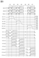
- 3A and 3B are timing charts showing an operation example of the display device.
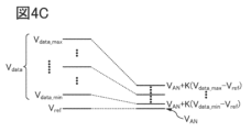
- 4A to 4C are diagrams showing potential relationships between an image data signal input to a circuit and an image data signal output from the circuit.
- FIG. 5 is a timing chart showing an operation example of the display device.
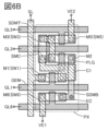
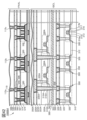
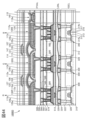
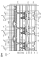
- 6A and 6B are plan views showing circuit layout examples.
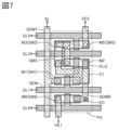
- FIG. 7 is a plan view showing a circuit layout example.
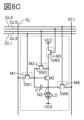
- 8A to 8C are circuit diagrams showing configuration examples of pixels included in the display device.
- FIG. 9 is a circuit diagram showing a configuration example of a display device.
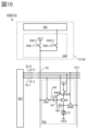
- FIG. 10 is a circuit diagram showing a configuration example of a display device.
- FIG. 10 is a circuit diagram showing a configuration example of a display device.
- FIG. 11 is a circuit diagram showing a configuration example of a display device.
- FIG. 12 is a circuit diagram showing a configuration example of a display device.
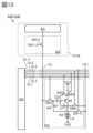
- FIG. 13 is a circuit diagram showing a configuration example of a display device.
- FIG. 14 is a circuit diagram showing a configuration example of a display device.
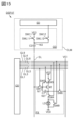
- FIG. 15 is a circuit diagram showing a configuration example of a display device.
- FIG. 16 is a timing chart showing an operation example of the display device.
- FIG. 17 is a circuit diagram showing a configuration example of a display device.
- 18A to 18C are timing charts showing operation examples of the display device.
- 19A to 19C are diagrams showing potential relationships between an image data signal input to a circuit and an image data signal output from the circuit.
- FIG. 20 is a plan view showing a circuit layout example.
- FIG. 21 is a circuit diagram showing a configuration example of a display device.
- FIG. 22 is a circuit diagram showing a configuration example of a display device.
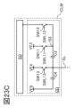
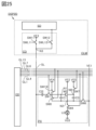
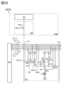
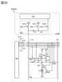
- 23A to 23D are circuit diagrams showing configuration examples of circuits included in the display device.
- FIG. 24 is a circuit diagram showing a configuration example of a display device.
- FIG. 25 is a circuit diagram showing a configuration example of a display device.
- FIG. 26 is a circuit diagram showing a configuration example of a display device.
- FIG. 27 is a circuit diagram showing a configuration example of a display device.
- FIG. 28 is a circuit diagram showing a configuration example of a display device.
- FIG. 29 is a circuit diagram showing a configuration example of a display device.
- FIG. 30 is a circuit diagram showing a configuration example of a display device.
- FIG. 31 is a timing chart showing an operation example of the display device.
- 32A to 32C are schematic cross-sectional views showing configuration examples of display devices.
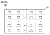
- FIG. 33A is a schematic plan view showing an example of a display portion of a display device
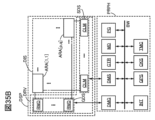
- FIG. 33B is a schematic plan view showing an example of a drive circuit region of the display device.
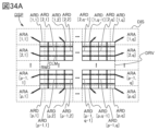
- 34A and 34B are schematic plan views showing configuration examples of the display device.
- 35A and 35B are block diagrams showing configuration examples of the display device.
- FIG. 36 is a schematic cross-sectional view showing a configuration example of a display device.
- 37A to 37C are schematic cross-sectional views showing a partial region of the configuration example of the display device.
- FIG. 38 is a schematic cross-sectional view showing a configuration example of a display device.
- FIG. 39 is a schematic cross-sectional view showing a configuration example of a display device.
- FIG. 40 is a schematic cross-sectional view showing a configuration example of a display device.
- FIG. 41 is a schematic cross-sectional view showing a configuration example of a display device.
- FIG. 42 is a schematic cross-sectional view showing a configuration example of a display device.
- 43A is a schematic cross-sectional view showing a configuration example of a display device, and FIGS. 43B and 43C are cross-sectional views showing configuration examples of a transistor.
- FIG. 44 is a schematic cross-sectional view showing a configuration example of a display device.
- FIG. 45 is a schematic cross-sectional view showing a configuration example of a display device.
- FIG. 45 is a schematic cross-sectional view showing a configuration example of a display device.
- FIG. 46 is a schematic cross-sectional view showing a configuration example of a display device.
- FIG. 47A is a schematic cross-sectional view showing a configuration example of a display device
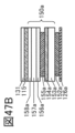
- FIG. 47B is a schematic cross-sectional view showing a configuration example of a light emitting device.
- FIG. 48 is a schematic cross-sectional view showing a configuration example of a display device.
- 49A to 49D are schematic cross-sectional views showing configuration examples of LED packages.
- 50A and 50B are schematic plan views showing configuration examples of LED packages.
- FIG. 51A is a schematic cross-sectional view showing a configuration example of a display device
- FIG. 51A is a schematic cross-sectional view showing a configuration example of a display device
- FIG. 51A is a schematic cross-sectional view showing a configuration example of a display device
- FIG. 51A is a schematic cross-sectional view showing a configuration example of a display device
- FIG. 51A is a schematic cross-sectional
- 51B is a schematic cross-sectional view showing a configuration example of a substrate provided in the display device and light-emitting diodes on the substrate.
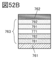
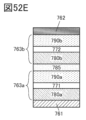
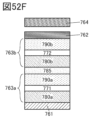
- 52A to 52F are diagrams showing configuration examples of light-emitting devices.
- 53A to 53C are diagrams showing configuration examples of light emitting devices.
- FIG. 54A is a circuit diagram showing a configuration example of a pixel circuit included in the display device
- FIG. 54B is a schematic perspective view showing a configuration example of the pixel circuit included in the display device.
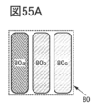
- 55A to 55G are plan views showing examples of pixels.
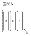
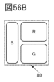
- 56A to 56F are plan views showing examples of pixels.
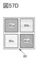
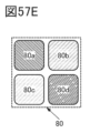
- 57A to 57H are plan views showing examples of pixels.
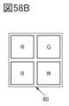
- 58A to 58D are plan views showing examples of pixels.
- FIG. 60A is a schematic plan view showing a configuration example of a transistor
- FIGS. 60B and 60C are schematic cross-sectional views showing configuration examples of the transistor.
- 61A and 61B are diagrams showing configuration examples of the display module.
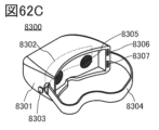
- 62A to 62F are diagrams showing configuration examples of electronic devices.
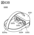
- 63A to 63D are diagrams illustrating configuration examples of electronic devices.
- 64A to 64C are diagrams illustrating configuration examples of electronic devices.
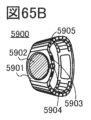
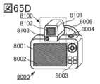
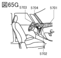
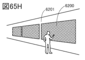
- 65A to 65H are diagrams illustrating configuration examples of electronic devices.
- a semiconductor device is a device that utilizes semiconductor characteristics, and refers to a circuit that includes semiconductor elements (eg, transistors, diodes, and photodiodes), and a device that has the same circuit.
- a semiconductor device refers to all devices that can function by utilizing semiconductor characteristics.
- an integrated circuit, a chip including the integrated circuit, and an electronic component containing the chip in a package are examples of semiconductor devices.
- storage devices, display devices, light-emitting devices, lighting devices, and electronic devices themselves may be semiconductor devices or may include semiconductor devices.
- connection relationships other than the connection relationships shown in the drawings or the text are not limited to the predetermined connection relationships, for example, the connection relationships shown in the drawings or the text.
- X and Y are electrically connected is an element that enables electrical connection between X and Y (for example, switch, transistor, capacitive element, inductor, resistive element, diode, display devices, light emitting devices, and loads) can be connected between X and Y one or more times.
- the switch has a function of being controlled to be turned on and off. In other words, the switch has the function of being in a conducting state (on state) or a non-conducting state (off state) and controlling whether or not to allow current to flow.
- both an element and a power supply line for example, VDD (high power supply potential), VSS (low power supply potential), GND (ground potential), or a wiring that gives a desired potential
- VDD high power supply potential
- VSS low power supply potential
- GND ground potential
- X and Y are electrically connected when they are connected.
- X and Y are directly connected.
- X and Y are electrically connected when the drain and source of the transistor are interposed between X and Y.
- a capacitive element when a capacitive element is arranged between X and Y, it may or may not be defined that X and Y are electrically connected.
- a capacitive element in the configuration of a digital circuit or logic circuit, if a capacitive element is arranged between X and Y, it may not be defined that X and Y are electrically connected.
- X and Y may be defined as being electrically connected.
- X and Y are functionally connected is a circuit that enables functional connection between X and Y (e.g., logic circuit (e.g., inverter, NAND circuit, and NOR circuit), Signal conversion circuits (e.g., digital-to-analog conversion circuits, analog-to-digital conversion circuits, and gamma correction circuits), potential level conversion circuits (e.g., power supply circuits such as step-up circuits or step-down circuits, and level shifter circuits that change the potential level of signals), voltage source, current source, switching circuit, amplifier circuit (for example, a circuit that can increase signal amplitude or current amount, operational amplifier, differential amplifier circuit, source follower circuit, and buffer circuit), signal generation circuit, memory circuit, and control circuit ) can be connected between X and Y one or more times. As an example, even if another circuit is interposed between X and Y, when a signal output from X is transmitted to Y, X and Y are considered to be functionally
- X and Y, and the source (which may be referred to as one of the first terminal or the second terminal) and the drain (which may be referred to as the other of the first terminal or the second terminal) of the transistor are , are electrically connected to each other, and are electrically connected in the order of X, the source of the transistor, the drain of the transistor, and Y.”
- the source of the transistor is electrically connected to X
- the drain of the transistor is electrically connected to Y
- X, the source of the transistor, the drain of the transistor, Y are electrically connected in that order.
- X is electrically connected to Y through the source and drain of the transistor, and X, the source of the transistor, the drain of the transistor, and Y are provided in this connection order.”
- X and Y are objects (for example, devices, elements, circuits, wiring, electrodes, terminals, conductive films, or layers).
- circuit diagram shows independent components electrically connected to each other, if one component has the functions of multiple components.
- one component has the functions of multiple components.
- the term "electrically connected" in this specification includes cases where one conductive film functions as a plurality of constituent elements.
- a “resistive element” can be, for example, a circuit element having a resistance value higher than 0 ⁇ or a wiring having a resistance value higher than 0 ⁇ . Therefore, in this specification and the like, a “resistive element” includes a wiring having a resistance value, a transistor, a diode, or a coil through which a current flows between a source and a drain.
- resistive element may be interchanged with the terms “resistance,””load,” or “region having a resistance value.”
- the terms “resistor,””load,” or “region having a resistance value” may be interchanged with the term “resistive element.”
- the resistance value can be, for example, preferably 1 m ⁇ or more and 10 ⁇ or less, more preferably 5 m ⁇ or more and 5 ⁇ or less, still more preferably 10 m ⁇ or more and 1 ⁇ or less. Also, for example, it may be 1 ⁇ or more and 1 ⁇ 10 9 ⁇ or less.
- capacitor element refers to, for example, a circuit element having a capacitance value higher than 0 F, a wiring region having a capacitance value higher than 0 F, a parasitic capacitance, or It can be the gate capacitance of a transistor. Also, the terms “capacitance element”, “parasitic capacitance”, or “gate capacitance” may be interchanged with the term “capacitance”.
- capacitor may be interchanged with the terms “capacitive element,” “parasitic capacitance,” or “gate capacitance.”
- a “capacity” (including a “capacity” with three or more terminals) includes an insulator and a pair of conductors sandwiching the insulator. Therefore, the term “pair of conductors” in “capacitance” can be replaced with “pair of electrodes,” “pair of conductive regions,” “pair of regions,” or “pair of terminals.” Also, the terms “one of a pair of terminals” and “the other of a pair of terminals” may be referred to as a first terminal and a second terminal, respectively.
- the value of the capacitance can be, for example, 0.05 fF or more and 10 pF or less. Also, for example, it may be 1 pF or more and 10 ⁇ F or less.
- a transistor has three terminals called a gate, a source, and a drain.
- a gate is a control terminal that controls the conduction state of a transistor.
- the two terminals functioning as source or drain are the input and output terminals of the transistor.
- One of the two input/output terminals functions as a source and the other as a drain depending on the conductivity type (n-channel type or p-channel type) of the transistor and the level of potentials applied to the three terminals of the transistor. Therefore, in this specification and the like, the terms “source” and “drain” may be used interchangeably.
- a transistor may have a back gate in addition to the three terminals described above, depending on the structure of the transistor.
- one of the gate and back gate of the transistor may be referred to as a first gate
- the other of the gate and back gate of the transistor may be referred to as a second gate.
- the terms "gate” and “backgate” may be used interchangeably for the same transistor.
- the respective gates may be referred to as a first gate, a second gate, a third gate, or the like in this specification and the like.
- a multi-gate transistor having two or more gate electrodes can be used as an example of a transistor.
- the multi-gate structure since the channel formation regions are connected in series, a structure in which a plurality of transistors are connected in series is obtained. Therefore, the multi-gate structure can reduce off-state current and improve the breakdown voltage (reliability) of the transistor.
- the multi-gate structure even if the voltage between the drain and source changes when operating in the saturation region, the current between the drain and source does not change much and the slope is flat. properties can be obtained.
- the flat-slope voltage-current characteristic an ideal current source circuit or an active load with a very high resistance value can be realized. As a result, a differential circuit or current mirror circuit with good characteristics can be realized.
- circuit elements such as “light-emitting device” and “light-receiving device” may have polarities called “anode” and “cathode”.
- anode In the case of a “light emitting device”, it may be possible to cause the “light emitting device” to emit light by applying a forward bias (applying a positive potential to the "anode” with respect to the "cathode”).
- the “anode” and “cathode” are sometimes treated as input/output terminals in circuit elements such as “light-emitting device” and “light-receiving device”.
- anode and “cathode” in circuit elements such as “light-emitting device” and “light-receiving device” are sometimes referred to as terminals (first terminal, second terminal, etc.).
- terminals first terminal, second terminal, etc.
- one of the “anode” and the “cathode” may be referred to as the first terminal, and the other of the “anode” and the “cathode” may be referred to as the second terminal.
- the circuit element may have a plurality of circuit elements.
- the circuit element when one resistor is described on the circuit diagram, it includes the case where two or more resistors are electrically connected in series.
- the case where one capacitor is described on the circuit diagram includes the case where two or more capacitors are electrically connected in parallel.
- the switch when one transistor is illustrated in a circuit diagram, two or more transistors are electrically connected in series and the gates of the transistors are electrically connected to each other. shall include Similarly, for example, when one switch is described on the circuit diagram, the switch has two or more transistors, and the two or more transistors are electrically connected in series or in parallel. and the gates of the respective transistors are electrically connected to each other.
- a node can be called a terminal, a wiring, an electrode, a conductive layer, a conductor, an impurity region, or the like, depending on the circuit configuration and device structure. Terminals, wirings, and the like can also be called nodes.
- Voltage is a potential difference from a reference potential.
- the reference potential is ground potential
- “voltage” can be replaced with “potential”. Note that the ground potential does not necessarily mean 0V.
- the potential is relative, and when the reference potential changes, the potential applied to the wiring, the potential applied to the circuit, etc., and the potential output from the circuit etc. also change.
- high-level potential and low-level potential do not mean specific potentials.
- the high-level potentials supplied by both wirings do not have to be equal to each other.
- the low-level potentials applied by both wirings need not be equal to each other.
- electrical current refers to the movement phenomenon of charge (electrical conduction).
- electrical conduction occurs in a positive In other words, “electrical conduction is occurring”. Therefore, in this specification and the like, unless otherwise specified, the term “electric current” refers to a charge transfer phenomenon (electrical conduction) associated with the movement of carriers.
- carriers here include electrons, holes, anions, cations, and complex ions, and the carriers differ depending on the current-flowing system (eg, semiconductor, metal, electrolyte, and in vacuum).
- the "direction of current” in wiring or the like is the direction in which carriers that become positive charges move, and is described as a positive amount of current.
- the direction in which the carriers that become negative charges move is the direction opposite to the direction of the current, and is represented by the amount of negative current. Therefore, in this specification and the like, when there is no notice about the positive or negative of the current (or the direction of the current), the description of "current flows from the element A to the element B" should be rephrased as “current flows from the element B to the element A.” It shall be possible. Also, the description of "a current is input to the element A" can be rephrased as "a current is output from the element A”.
- ordinal numbers such as “first”, “second”, and “third” are added to avoid confusion of constituent elements. Therefore, the number of components is not limited. Also, the order of the components is not limited. For example, the component referred to as “first” in one of the embodiments such as this specification may be the component referred to as “second” in another embodiment or the scope of claims. can also be Further, for example, the component referred to as “first” in one of the embodiments of this specification etc. may be omitted in other embodiments or the scope of claims.
- the terms “above” and “below” do not limit the positional relationship of the components to being directly above or below and in direct contact with each other.
- the expression “electrode B on insulating layer A” does not require that electrode B be formed on insulating layer A in direct contact with another configuration between insulating layer A and electrode B. Do not exclude those containing elements.
- the expression “electrode B above the insulating layer A” it is not necessary that the electrode B is formed on the insulating layer A in direct contact with the insulating layer A and the electrode B.
- Electrode B under the insulating layer A it is not necessary that the electrode B is formed under the insulating layer A in direct contact with the insulating layer A and the electrode B. do not exclude other components between
- the terms “row” and “column” may be used to describe the components arranged in a matrix and their positional relationships.
- the positional relationship between the configurations changes appropriately according to the direction in which each configuration is drawn. Therefore, it is not limited to the words and phrases explained in the specification, etc., and can be appropriately rephrased according to the situation.
- the expression “row-wise” may be rephrased as “column-wise” by rotating the orientation of the drawing shown by 90 degrees.
- a wiring that electrically connects components arranged in a matrix can extend in the row direction or the column direction.
- the wiring A may also extend in the column direction.
- the wiring A may also extend in the row direction. That is, the direction in which the wiring that electrically connects the components arranged in a matrix is not limited to the direction described in this specification and the like, and can be the row direction or the column direction.
- the terms “film” and “layer” can be interchanged depending on the situation. For example, it may be possible to change the term “conductive layer” to the term “conductive film.” Or, for example, it may be possible to change the term “insulating film” to the term “insulating layer”. Alternatively, the terms “film” and “layer” may be omitted and replaced with other terms as the case may or may be. For example, it may be possible to change the term “conductive layer” or “conductive film” to the term “conductor.” Or, for example, it may be possible to change the term “insulating layer” or “insulating film” to the term “insulator”.
- electrode in this specification do not functionally limit these components.
- an “electrode” may be used as part of a “wiring” and vice versa.
- the term “electrode” or “wiring” includes the case where a plurality of “electrodes” or “wiring” are integrally formed.
- a “terminal” may be used as part of a “wiring” or an “electrode”, and vice versa.
- terminal includes the case where one or more selected from “electrode”, “wiring”, and “terminal” are integrally formed.
- an “electrode” can be part of a “wiring” or a “terminal”, and a “terminal” can be part of a “wiring” or an “electrode”, for example.
- the terms “electrode”, “wiring”, or “terminal” may be replaced with the term “region” in some cases.
- the terms “wiring”, “signal line”, and “power line” can be interchanged depending on the case or situation. For example, it may be possible to change the term “wiring” to the term “signal line”. Also, for example, it may be possible to change the term “wiring” to a term such as "power supply line”. Also, vice versa, it may be possible to change the term “signal line” or “power line” to the term “wiring”. It may be possible to change the term "power line” to the term “signal line”. Also, vice versa, the term “signal line” may be changed to the term "power line”. Also, the term “potential” applied to the wiring can be changed to the term “signal” in some cases or depending on the situation. And vice versa, the term “signal” may be changed to the term “potential”.
- timing charts are sometimes used to describe the operation method of the semiconductor device.
- the timing charts used in this specification and the like show ideal operation examples. is not limited unless otherwise specified.
- the magnitude and timing of signals (for example, potential or current) input to each wiring (including nodes) in the timing chart may be changed depending on the situation. It can be performed. For example, even if the timing chart shows two periods at equal intervals, the lengths of the two periods may differ from each other. Also, for example, in two periods, even if one period is long and the other period is described as short, the length of both periods may be equal, or one period may be short And the other period may be longer in some cases.
- a metal oxide is a metal oxide in a broad sense. Metal oxides are classified into oxide insulators, oxide conductors (including transparent oxide conductors), oxide semiconductors (also referred to as oxide semiconductors or simply OSs), and the like. For example, when a channel formation region of a transistor contains a metal oxide, the metal oxide is sometimes referred to as an oxide semiconductor. In other words, when a metal oxide can constitute a channel-forming region of a transistor having at least one of an amplifying action, a rectifying action, and a switching action, the metal oxide is called a metal oxide semiconductor. can do. In the case of describing an OS transistor, it can also be referred to as a transistor including a metal oxide or an oxide semiconductor.
- nitrogen-containing metal oxides may also be collectively referred to as metal oxides.
- a metal oxide containing nitrogen may also be referred to as a metal oxynitride.
- semiconductor impurities refer to, for example, substances other than the main component that constitutes the semiconductor layer.
- impurities may cause one or both of, for example, an increase in defect level density, a decrease in carrier mobility, and a decrease in crystallinity in a semiconductor.
- impurities that change the characteristics of the semiconductor include, for example, Group 1 elements, Group 2 elements, Group 13 elements, Group 14 elements, and Group 15 elements.
- transition metals other than the main constituents among others, for example, hydrogen (also contained in water), lithium, sodium, silicon, boron, phosphorus, carbon, and nitrogen.
- impurities that change the characteristics of the semiconductor include, for example, Group 1 elements, Group 2 elements, Group 13 elements, and Group 15 elements (with the exception of oxygen, does not contain hydrogen).
- a switch is one that has the function of being in a conducting state (on state) or a non-conducting state (off state) and controlling whether or not to allow current to flow.
- a switch has a function of selecting and switching a path through which current flows. Therefore, the switch may have two or more terminals through which current flows, in addition to the control terminal.
- an electrical switch, a mechanical switch, or the like can be used. In other words, the switch is not limited to a specific one as long as it can control current.
- Examples of electrical switches include transistors (eg, bipolar transistors, MOS transistors, etc.), diodes (eg, PN diodes, PIN diodes, Schottky diodes, MIM (Metal Insulator Metal) diodes, MIS (Metal Insulator Semiconductor) diodes , and diode-connected transistors), or a logic circuit combining these.
- transistors eg, bipolar transistors, MOS transistors, etc.
- diodes eg, PN diodes, PIN diodes, Schottky diodes, MIM (Metal Insulator Metal) diodes, MIS (Metal Insulator Semiconductor) diodes , and diode-connected transistors
- the “conducting state” of the transistor means, for example, a state in which the source electrode and the drain electrode of the transistor can be considered to be electrically short-circuited, or a state in which a current flows between the source electrode and the drain electrode.
- a “non-conducting state” of a transistor means a state in which a source electrode and a drain electrode of the transistor can be considered to be electrically cut off. Note that the polarity (conductivity type) of the transistor is not particularly limited when the transistor is operated as a simple switch.
- a mechanical switch is a switch using MEMS (Micro Electro Mechanical Systems) technology.
- the switch has an electrode that can be moved mechanically, and operates by controlling conduction and non-conduction by moving the electrode.
- a device manufactured using a metal mask or FMM may be referred to as a device with an MM (metal mask) structure.
- a device manufactured without using a metal mask or FMM may be referred to as a device with an MML (metal maskless) structure.
- a structure in which a light-emitting layer is separately formed or a light-emitting layer is separately painted in each color light-emitting device is referred to as SBS (Side By Side) structure.
- SBS Side By Side
- a light-emitting device capable of emitting white light is sometimes referred to as a white light-emitting device.
- the white light-emitting device can be combined with a colored layer (for example, a color filter) to form a full-color display device.
- light-emitting devices can be broadly classified into single structures and tandem structures.
- a single-structure device preferably has one light-emitting unit between a pair of electrodes, and the light-emitting unit preferably includes one or more light-emitting layers.
- light-emitting layers may be selected such that the respective colors of light emitted from the two light-emitting layers are in a complementary color relationship.
- the luminescent color of the first luminescent layer and the luminescent color of the second luminescent layer have a complementary color relationship, it is possible to obtain a configuration in which the entire light emitting device emits white light.
- the light-emitting device as a whole may emit white light by combining the light-emitting colors of the three or more light-emitting layers.
- a device with a tandem structure preferably has two or more light-emitting units between a pair of electrodes, and each light-emitting unit includes one or more light-emitting layers.
- each light-emitting unit includes one or more light-emitting layers.
- a structure in which white light emission is obtained by combining light from the light emitting layers of a plurality of light emitting units may be employed. Note that the structure for obtaining white light emission is the same as the structure of the single structure.
- the white light emitting device when comparing the white light emitting device (single structure or tandem structure) and the light emitting device having the SBS structure, the light emitting device having the SBS structure can consume less power than the white light emitting device. If it is desired to keep power consumption low, it is preferable to use a light-emitting device with an SBS structure. On the other hand, the white light emitting device is preferable because the manufacturing process is simpler than that of the SBS structure light emitting device, so that the manufacturing cost can be lowered or the manufacturing yield can be increased.
- parallel refers to a state in which two straight lines are arranged at an angle of -10° or more and 10° or less. Therefore, the case of ⁇ 5° or more and 5° or less is also included.
- substantially parallel or “substantially parallel” refers to a state in which two straight lines are arranged at an angle of -30° or more and 30° or less.
- Perfect means that two straight lines are arranged at an angle of 80° or more and 100° or less. Therefore, the case of 85° or more and 95° or less is also included.
- the content (or part of the content) described in one embodiment may be combined with another content (or part of the content) described in that embodiment, or one or a plurality of other implementations. can be applied, combined, or replaced with at least one of the contents described in the form of (may be part of the contents).
- figure (may be part of) described in one embodiment refers to another part of that figure, another figure (may be part) described in that embodiment, and one or more other More drawings can be formed by combining at least one of the drawings (or part of them) described in the embodiments.
- plan views may be used to describe the configuration according to each embodiment.
- a plan view is, for example, a diagram showing a state of a plane (cut end) obtained by cutting the configuration in the horizontal direction.
- Hidden lines for example, dashed lines
- the term "plan view” can be replaced with the term "projection view", "top view", or "bottom view”.
- a plane (cut) obtained by cutting the configuration in a direction different from the horizontal direction may be called a plan view instead of a plane (cut) obtained by cutting the configuration in the horizontal direction.
- cross-sectional views may be used to describe the configuration according to each embodiment.
- a cross-sectional view is, for example, a diagram showing a state of a plane (cut end) obtained by cutting the configuration in the vertical direction.
- the term "cross-sectional view” can be replaced with the term "front view” or "side view”.
- a cross-sectional view may be a plane (cut) obtained by cutting the structure in a direction different from the vertical direction, rather than a plane (cut) obtained by cutting the configuration in the vertical direction.
- FIG. 1 shows a display device of one embodiment of the present invention.
- the display device DSP0 has, as an example, a pixel array ALP, a row driver circuit RWD, and a column driver circuit CLM.
- the pixel array ALP has, for example, m ⁇ n pixels PX (where m is an integer of 1 or more and n is an integer of 1 or more).
- the pixels PX are arranged in a matrix of m rows and n columns in the pixel array ALP.
- FIG. 1 illustrates a plurality of pixels PX as a pixel PX[1,1], a pixel PX[m,1], a pixel PX[1,n], a pixel PX[m,n], a pixel PX[i,j] (where i is an integer of 1 to m and j is an integer of 1 to n) is shown.
- the pixel PX functions as a display pixel.
- a display pixel can be, for example, a pixel to which one or both of a liquid crystal display device and a light-emitting device are applied.
- Examples of light-emitting devices include light-emitting devices including organic EL elements (OLEDs (Organic Light Emitting Diodes)), inorganic EL elements, LEDs (including micro LEDs), QLEDs (Quantum-dot Light Emitting Diodes), and semiconductor lasers. is mentioned. Note that in this embodiment, a light-emitting device including an organic EL material is applied to the pixel PX.
- the luminance of light emitted from a light emitting device capable of emitting light with particularly high luminance is, for example, 500 cd/m 2 or more, preferably 1000 cd/m 2 or more and 10000 cd/m 2 or less, more preferably 2000 cd/m 2 or more and 5000 cd/m 2 or more. m 2 or less.
- each of the wirings GL[1] to GL[m] extends in the row direction.
- each of the wirings SL[1] to SL[n] extends in the column direction.
- the pixel PX[i,j] is electrically connected to the wiring GL[i] and the wiring SL[j], for example.
- the wiring SL[j] functions, for example, as a wiring that transmits an image data signal to the pixel PX[i, j].
- FIG. 1 illustrates that one wiring SL extends per column in the pixel array, but the number of wirings SL extending in one column is not limited to one. . That is, the number of wirings SL extending in one column of the pixel array ALP may be two or more.
- the wiring GL[i] functions, for example, as a wiring that transmits a selection signal for selecting the pixel PX[i,j] to which the image data signal is supplied. Further, the wiring GL[i] is, for example, a selection line for selecting the pixel PX[i,j] in order to correct the threshold voltage of the drive transistor included in the pixel PX[i,j]. It may also function as wiring for transmitting signals. The wiring GL[i] also functions as a wiring for transmitting a control signal (digital potential) for switching the switch included in the pixel PX[i,j] between an on state and an off state. good too.
- FIG. 1 illustrates that one wiring GL extends per row in the pixel array, but the number of wirings GL extending per row is not limited to one. . That is, the number of wirings GL extending in one row of the pixel array ALP may be two or more. For example, the number of wirings GL extending in one row can be determined according to the circuit configuration of the pixel PX, and the number of wirings GL may be two or more depending on the circuit configuration of the pixel PX.
- the row driver circuit RWD has, for example, a drive circuit GD.
- the driver circuit GD is electrically connected to each of the wirings GL[1] to GL[m].
- the driving circuit GD selects one or more selected from the first to m-th rows of the pixel array ALP to which the image data signal is supplied, and selects one or more pixels arranged in the selected row. It has a function of transmitting a selection signal to the pixel PX. For this reason, the drive circuit GD may be provided with a demultiplexer. Note that the selection signal can be, for example, an analog potential, a digital potential (a high-level potential or a low-level potential), or a pulse potential. Further, the driving circuit GD not only selects the pixel PX to which the image data signal is supplied, but also has a function of selecting the pixel PX for the purpose of correcting the threshold voltage of the transistor included in the pixel PX. may have. That is, the drive circuit GD may have a function of transmitting a selection signal for correcting the threshold voltage of the transistor included in the pixel PX.
- the column driver circuit CLM has, for example, a drive circuit SD and circuits CD[1] to CD[n].
- each of the circuits CD[1] to CD[j] is electrically connected to the driving circuit SD. Further, the circuit CD[j] is electrically connected to the wiring SL[j], for example.
- the drive circuit SD has, for example, a function of transmitting image data signals to the pixels PX included in the pixel array ALP. Further, depending on the transmission method of the image data signal, the drive circuit SD may be provided with a demultiplexer. Note that the image data signal can be, for example, an analog potential, a digital potential (high-level potential or low-level potential), or a pulse potential.
- the circuit CD[j] has a function of level-shifting the image data signal input from the drive circuit SD and transmitting the level-shifted image data signal to the line SL[j].
- the display device DSP1A shown in FIG. 2 is an example of the display device DSP0 shown in FIG.
- the drive circuit GD of the row driver circuit RWD and the circuit CD and drive circuit SD of the column driver circuit CLM, which are connected, are shown in an excerpt.
- the pixel PX has, for example, a transistor M2, a switch SW1, a switch SW3, a switch SW5, a switch SW6, a capacitor C1, and a light emitting device LD.
- the circuit CD also has a switch SW11, a switch SW12, and a capacitor C2.
- transistor M2 functions as a driving transistor in pixel PX.
- an OS transistor is preferably applied to the transistor M2.
- metal oxides included in the channel formation region of the OS transistor include indium oxide, gallium oxide, and zinc oxide.
- the metal oxide preferably contains one or more selected from indium, the element M, and zinc.
- Element M includes gallium, aluminum, silicon, boron, yttrium, tin, copper, vanadium, beryllium, titanium, iron, nickel, germanium, zirconium, molybdenum, lanthanum, cerium, neodymium, hafnium, tantalum, tungsten, cobalt, and magnesium.
- the element M is preferably one or more selected from aluminum, gallium, yttrium, and tin.
- an oxide containing indium (In), gallium (Ga), and zinc (Zn) also referred to as IGZO
- an oxide containing indium, tin, and zinc also referred to as ITZO (registered trademark)
- ITZO registered trademark
- oxides containing indium, gallium, tin, and zinc are preferably used.
- an oxide containing indium (In), aluminum (Al), and zinc (Zn) is preferably used.
- an oxide containing indium (In), aluminum (Al), gallium (Ga), and zinc (Zn) also referred to as IAGZO
- IAGZO oxide containing indium (In), aluminum (Al), gallium (Ga), and zinc (Zn)
- the OS transistor will be described in detail in Embodiment 5.
- a transistor other than the OS transistor may be applied to the transistor M2.
- a transistor including silicon in a channel formation region (hereinafter referred to as a Si transistor) can be applied to the transistor M2.
- silicon for example, single crystal silicon, amorphous silicon (sometimes referred to as hydrogenated amorphous silicon), microcrystalline silicon, or polycrystalline silicon (including low-temperature polycrystalline silicon) can be used.
- the transistor M2 includes, for example, a transistor whose channel formation region contains germanium, zinc selenide, cadmium sulfide, gallium arsenide, indium phosphide, gallium nitride, or silicon.
- a transistor whose channel formation region contains a compound semiconductor such as germanium, a transistor whose channel formation region contains a carbon nanotube, or a transistor whose channel formation region contains an organic semiconductor can be used.
- the transistor M2 illustrated in FIG. 2 is an n-channel transistor, it may be a p-channel transistor depending on the situation or circumstances. Further, when the n-channel transistor is replaced with the p-channel transistor, it is necessary to appropriately change the potential input to the pixel PX so that the pixel PX operates normally. Note that this applies not only to FIG. 2 but also to transistors described elsewhere in the specification or illustrated in other drawings. Further, in this embodiment mode, the structure and operation of the pixel PX are described with the transistor M2 being an n-channel transistor.
- the transistor M2 operates to flow a current between the source and the drain according to the voltage between the gate and the source instead of the voltage between the source and the drain. That is, it is preferable that the transistor M2 operates in the saturation region when it is on. By operating transistor M2 in the saturation region, the amount of current flowing through transistor M2 can be determined by the gate-to-source voltage. Further, by operating the transistor M2 in the saturation region, even if the source-drain voltage of the transistor M2 changes, the drain current does not change significantly. That is, by determining the amount of current flowing through the transistor M2 by the gate-source voltage, the transistor M2 can allow a stable current to flow between the anode and cathode of the light emitting device LD. Also, in some circumstances, transistor M2 may operate in its linear region when it is on. Alternatively, transistor M2 may operate in the sub-threshold region.
- switches SW1, SW3, SW5, SW6, SW11, and SW12 can be applied to each of the switches SW1, SW3, SW5, SW6, SW11, and SW12.
- the switches SW1, SW3, SW5, SW6, SW11, and SW12 preferably use the above-described transistors as electrical switches, and OS transistors are used. is more preferable.
- the electrical switches other than the OS transistor include: A transistor that can be applied to the transistor M2 can be used.
- the transistor can be a Si transistor.
- mechanical switches may be applied to the switches SW1, SW3, SW5, SW6, SW11, and SW12.
- each of the switches SW1, SW3, SW5, SW6, SW11, and SW12 shown in FIG. It is turned on when it is on, and turned off when a low level potential is applied to the control terminal.
- the light-emitting device LD is, for example, a self-luminous light-emitting device having an organic EL element (OLED).
- OLED organic EL element
- the first terminal of the switch SW1 is electrically connected to the gate of the transistor M2, the first terminal of the switch SW3, and the first terminal of the capacitor C1, and the second terminal of the switch SW1 is connected to the wiring.
- SL and the control terminal of the switch SW1 is electrically connected to the wiring GL1.
- the first terminal of the transistor M2 is electrically connected to the second terminal of the capacitor C1, the first terminal of the switch SW6, and the anode of the light emitting device LD, and the second terminal of the transistor M2 is connected to the switch SW3. and the first terminal of the switch SW5.
- a control terminal of the switch SW3 is electrically connected to the wiring GL3.
- a second terminal of the switch SW5 is electrically connected to the wiring VE2, and a control terminal of the switch SW5 is electrically connected to the wiring GL5.
- a second terminal of the switch SW6 is electrically connected to the wiring VE1, and a control terminal of the switch SW6 is electrically connected to the wiring GL6.
- the cathode of the light emitting device LD is electrically connected to the wiring VE0.
- an electrical connection point between the first terminal of the switch SW1, the first terminal of the switch SW3, the gate of the transistor M2, and the first terminal of the capacitor C1 is referred to as a node N1.
- a node N2 is an electrical connection point among the first terminal of the transistor M2, the second terminal of the capacitor C1, the first terminal of the switch SW6, and the anode of the light emitting device LD.
- a first terminal of the capacitor C2 is electrically connected to the wiring SL, and a second terminal of the capacitor C2 is electrically connected to the first terminal of the switch SW11 and the first terminal of the switch SW12. It is A second terminal of the switch SW11 is electrically connected to the wiring VE3, and a control terminal of the switch SW11 is electrically connected to the wiring SWL11. A second terminal of the switch SW12 is electrically connected to the drive circuit SD, and a control terminal of the switch SW12 is electrically connected to the wiring SWL12.
- an electrical connection point between the first terminal of the switch SW11, the first terminal of the switch SW12, and the second terminal of the capacitor C2 is called a node N3.
- Each of the wirings VE0 to VE3 functions as a wiring for applying a constant potential, for example.
- the constant potentials applied to the wirings VE0 to VE3 may be the same or different. Alternatively, some of the potentials applied to the wirings VE0 to VE3 may be the same and the rest may be different. Further, one or more wirings selected from the wirings VE0 to VE3 may function as wirings for applying a pulse potential instead of a constant potential.
- the wiring VE0 preferably functions as a wiring that applies a potential to the cathode of the light emitting device LD.
- the wiring VE2 preferably functions as a wiring that applies a potential to the anode of the light emitting device LD.
- the cathode of the light emitting device LD is electrically connected to the wiring VE0, and the anode of the light emitting device LD is electrically connected to the wiring VE2 via the transistor M2 and the switch SW5.
- the anode of the light emitting device LD may be electrically connected to the wiring VE0, and the cathode of the light emitting device LD may be electrically connected to the wiring VE2. That is, when the former light-emitting device LD has a forward stacking structure, the light-emitting device of the pixel in the display device of one embodiment of the present invention may have a reverse stacking structure.
- the wiring VE0 functions as a wiring that applies a potential to the anode of the light emitting device LD
- the wiring VE2 functions as a wiring that applies a potential to the cathode of the light emitting device LD.
- the wiring GL1, the wiring GL3, the wiring GL5, and the wiring GL6 correspond to one of the wirings GL[1] to GL[m] in FIG. That is, in the case of the circuit configuration of the pixel PX shown in FIG. 2, the number of wirings GL extending to one row of the pixel array ALP is four.
- the wiring SWL11 functions as a wiring for transmitting a control signal (digital potential) for switching the switch SW11 between the ON state and the OFF state.
- the wiring SWL12 functions as a wiring for transmitting a control signal (digital potential) for switching the switch SW12 between the ON state and the OFF state.
- FIG. 3A and 3B are timing charts showing an example of the operation method of the display device DSP1A.
- the timing chart in FIG. 3A shows changes in the potentials of the wiring GL1, the wiring GL3, the wiring GL5, the wiring GL6, the wiring SWL11, the wiring SWL12, and the node N3 in each of the periods T11 to T17.
- FIG. 3B shows changes in the potentials of the node N1 and the node N2 in each of the periods T11 to T17.
- the potential change of the node N1 is indicated by a solid line
- the potential change of the node N2 is indicated by a dashed line.
- the timing chart of FIG. 3B shows a case where the threshold voltage of the transistor M2 is higher than 0V.
- High indicates a high level potential and Low indicates a low level potential.
- VN is applied as a constant potential to the wiring VE1. Further, Vref is applied as a constant potential to the wiring VE3. Note that VN and Vref may have the same potential.
- VAN is applied as a constant potential to the wiring VE2. It is assumed that VCT is applied to the wiring VE0 as a constant potential. In addition, V AN is set to a potential higher than V CT .
- VAN has a higher potential than VN .
- VN - VCT is a voltage at which the light-emitting device LD does not emit light (current does not flow between the anode and ni-cathode of the light-emitting device LD). Therefore , VN is preferably equal to or lower than VCT .
- the threshold voltage of the transistor M2 is Vth .
- V th is a voltage lower than V AN ⁇ V N .
- the wiring GL1, the wiring GL3, the wiring GL5, the wiring GL6, the wiring SWL11, and the wiring SWL12 are each supplied with a low-level potential.
- a low level potential is applied to the respective control terminals of the switches SW1, SW3, SW5, SW6, SW11, and SW12, so that each of these switches is in an off state. .
- FIG. 3B shows an example in which the potential of the node N1 rises during a period T11, which will be described later. good. Further, for example, FIG. 3B shows an example in which the potential of the node N2 is lowered in a period T11 described later, but the potential of the node N2 before the period T11 is a potential that rises in the period T11. may be
- the potential of the node N3 is indefinite. Therefore, the potential of the node N3 before the period T11 in the timing chart of FIG. 3A is shown hatched.
- Period T11 In the period T11, a high-level potential is applied to the wirings GL1, GL3, GL5, GL6, and SWL11. As a result, high-level potentials are applied to the control terminals of the switches SW1, SW3, SW5, SW6, and SW11, so that these switches are turned on.
- the switch SW6 since the switch SW6 is in the ON state, the wiring VE1 and the first terminal of the transistor M2, the second terminal of the capacitor C1, and the anode of the light emitting device LD are electrically connected. Therefore, the potential VN from the wiring VE1 is applied to the first terminal of the transistor M2, the second terminal of the capacitor C1, and the anode (node N2) of the light emitting device LD (see FIG. 3B).
- the voltage between the anode and the cathode of the light emitting device LD is VN - VCT .
- the light-emitting device LD does not emit light (no current flows between the anode-cathode of the light-emitting device LD).
- the potential of the gate and the second terminal of the transistor M2 is VAN
- the potential of the first terminal of the transistor M2 is VN
- the gate-source voltage of the transistor M2 is VAN - VN . Since the gate-source voltage VAN - VN is higher than Vth , the transistor M2 is turned on. Also, assuming that no current flows between the anode and cathode of the light emitting device LD, current flows between the wiring VE1 and the wiring VE2 via the switch SW5, the transistor M2, and the switch SW6.
- a high-level potential is input to each of the wirings GL1, GL3, GL5, GL6, and SWL11 at the same timing in the period T11 in the timing chart of FIG. 3A;
- the timing at which the high-level potential is input to each of the wiring GL1, the wiring GL3, the wiring GL5, the wiring GL6, and the wiring SWL11 may be different.
- the transistor M2 is turned on because the gate-source voltage VAN - VN of the transistor M2 is higher than the threshold voltage Vth of the transistor M2.
- the potential V AN is no longer applied from the wiring VE2 to the second terminal of the transistor M2 and the gate of the transistor M2.
- the electric current is discharged to the wiring VE1 between the 1st terminal and the 2nd terminal and via the switch SW6. This lowers the potential of node N1.
- the gate-source voltage of the transistor M2 As the potential of the node N1 drops, the gate-source voltage of the transistor M2 also drops. When the voltage between the gate and the source of the transistor M2 is lowered to the threshold voltage Vth of the transistor M2, the transistor M2 is turned off and discharge of positive charges from the node N1 is stopped. That is, when the potential of the node N1 reaches VN + Vth from VAN , the transistor M2 is turned off. Since the transistor M2 is turned off, the potential of the node N1 remains unchanged from V N +V th (see FIG. 3B). Further, since the transistor M2 is turned off, the node N1 and the wiring SL are in a floating state.
- Period T13 In the period T13, a low-level potential is applied to each of the wiring GL3 and the wiring SWL11. As a result, a low level potential is applied to the control terminals of the switches SW3 and SW11, so that the switches SW3 and SW11 are turned off.
- the switch SW3 Since the switch SW3 is in the off state, the first terminal of the capacitor C2, the gate of the transistor M2, the first terminal of the capacitor C1, and the second terminal of the transistor M2 are in a non-conducting state.
- the drive circuit SD sends an image data signal corresponding to the image to be displayed on the pixel PX to the second terminal (node N3) of the capacitor C2 via the switch SW12. shall be sent.
- the image data signal is assumed to be the potential V data .
- the potential of the node N3 changes from Vref to Vdata .
- the potentials of the wiring SL and the node N1 change as the potential of the node N3 changes due to capacitive coupling in the capacitor C2.
- the amount of change in the potential of the wiring SL and the node N1 is, for example, the electrostatic capacitance of the capacitor C1, the electrostatic capacitance of the capacitor C2, the gate capacitance of the transistor M2, the parasitic capacitance related to the switch SW1, the parasitic capacitance related to the switch SW3, and the wiring. It is determined by the parasitic capacitance associated with SL. In this operation example, for the sake of simplicity, it is assumed that the amount of change in the potential of the wiring SL and the node N1 is determined by the capacitance of the capacitor C1 and the capacitance of the capacitor C2.
- the transistor M2 since the gate-source voltage V drv of the transistor M2 is higher than the threshold voltage V th of the transistor M2, the transistor M2 is turned on. However, since the switches SW3 and SW5 are off, the second terminal of the transistor M2 and the node N1 and the second terminal of the transistor M2 and the wiring VE2 are not electrically connected. becomes. Therefore, no current flows between the first terminal and the second terminal of the transistor M2.
- Period T15 A low-level potential is applied to the wiring GL1 in the period T15. As a result, a low level potential is applied to the control terminal of the switch SW1, so that the switch SW1 is turned off.
- Period T16 In the period T16, a high-level potential is applied to the wiring GL5 and a low-level potential is applied to the wiring GL6. As a result, a high level potential is applied to the control terminal of the switch SW5, so that the switch SW5 is turned on. Also, since a low level potential is applied to the control terminal of the switch SW6, the switch SW6 is turned off.
- the switch SW5 Since the switch SW5 is on, the second terminal of the transistor M2 and the wiring VE2 are electrically connected. Further, since the switch SW6 is in the off state, the wiring VE1 is not electrically connected to the first terminal of the transistor M2 and the second terminal of the capacitor C1. Also, since the switch SW3 has been in the off state since the period T13, the second terminal of the transistor M2 and the gate (node N1) of the transistor M2 are in a non-conducting state.
- the voltage V AN -V CT between the wiring VE0 and the wiring VE2 is divided by the transistor M2, the light emitting device LD, and the switch SW5.
- the potential of the first terminal of the transistor M2 (the second terminal of the capacitor C1 and the node N2) is boosted from VN to VS by the operation in the period T16 (see FIG. 3B). .
- the amount of change in the potential of the node N1 due to the capacitive coupling of the capacitor C1 described above is determined by the electrostatic capacitance of the capacitor C1, the gate capacitance of the transistor M2, the parasitic capacitance associated with the switch SW1, and the parasitic capacitance associated with the switch SW3.
- the amount of current that flows between the first terminal and the second terminal of transistor M2 depends on the gate-source voltage V drv of transistor M2.
- k is a proportionality constant that depends on the structure of the transistor.
- the transistor M2 can generate a current that does not depend on the threshold voltage Vth of the transistor M2.
- the potential of the anode of the light emitting device LD is VS
- the potential between the anode and the cathode of the light emitting device LD is VS - VCT .
- the light emitting device LD emits light.
- the luminance of the light-emitting device LD is determined by the amount of current flowing between the anode and cathode of the light-emitting device LD. That is, the light emission luminance of the light emitting device LD is determined by the image data signal V data input from the drive circuit SD.
- the image data signal V data output from the drive circuit SD changes to V AN +K ⁇ (V data ⁇ V ref ) through the circuit CD. That is, V AN +K ⁇ (V data ⁇ V ref ) is input to the pixel PX.
- K C 2 /(C 1 +C 2 ).
- the minimum pixel grayscale level is Vdata_min
- the maximum pixel grayscale level is Vdata_max
- the image data signal Vdata takes one of a plurality of potentials from Vdata_min to Vdata_max .
- Each of the plurality of potentials from Vdata_min to Vdata_max is input to the pixel PX via the circuit CD, so that VAN +K*( Vdata_min - Vref ) to VAN +K*( Vdata_max - Vref ). change to
- each of the image data signals Vdata_min to Vdata_max output from the drive circuit SD and VAN +K ⁇ ( Vdata_min ⁇ Vref ) to V AN +K ⁇ (V data_max ⁇ V ref ) is as shown in FIG. 4A. That is, by inputting the image data signal output from the driving circuit SD to the pixel PX via the circuit CD, the potential range of the image data signal is narrowed and the step width of the potential of the image data signal is also reduced. . As a result, the potential of the image data signal input to the pixel PX can be finely changed, so that the amount of current flowing between the source and the drain of the transistor M2 can be finely changed.
- each of the image data signals V data_min to V data_max output from the drive circuit SD and V AN +K ⁇ (V data_min ⁇ V ref ) to V AN +K ⁇ (V data_max ⁇ V ref ) is as shown in FIG. 4B. 4A in that the step size of the potential of the image data signal can be reduced to finely change the amount of current flowing between the source and the drain of the transistor M2.
- each of the image data signals V data_min to V data_max output from the drive circuit SD and V AN +K ⁇ (V data_min ⁇ Vref ) to VAN +K ⁇ ( Vdata_max ⁇ Vref ) is as shown in FIG. 4C. 4A and 4B in that the step size of the potential of the image data signal can be reduced to finely change the amount of current flowing between the source and the drain of the transistor M2.
- a high-level potential is input to the wiring GL5 and a low-level potential is input to the wiring GL6 at the same timing. and the wiring GL6 may be supplied with different timings.
- the wiring GL5 and the wiring SWL12 are each supplied with a low-level potential, and the wiring GL6 is supplied with a high-level potential. Therefore, a low-level potential is applied to the control terminals of the switches SW5 and SW12, so that the switches SW5 and SW12 are turned off. Also, since a high level potential is applied to the control terminal of the switch SW6, the switch SW6 is turned on.
- the switch SW5 Since the switch SW5 is off, the second terminal of the transistor M2 and the wiring VE2 are not electrically connected. Also, since the switch SW6 is in the ON state, the wiring VE1 and the first terminal of the transistor M2, the second terminal of the capacitor C1, and the anode of the light emitting device LD are electrically connected. Therefore, the potential VN from the wiring VE1 is applied to the first terminal of the transistor M2, the second terminal of the capacitor C1, and the anode (node N2) of the light emitting device LD (see FIG. 3B).
- the voltage between the anode and the cathode of the light emitting device LD is VN - VCT .
- the light-emitting device LD does not emit light (no current flows between the anode-cathode of the light-emitting device LD).
- the light emission of the light emitting device LD can be stopped.
- the transistor M2 of the pixel PX can generate current independent of the threshold voltage Vth of the transistor M2 and supply the current to the light emitting device LD. be able to.
- the threshold voltages of the driving transistors of the plurality of pixels included in the pixel array of the display device may vary depending on the manufacturing process and manufacturing environment of the display device. In other words, even if the same image data signal is supplied to different pixels, if the threshold voltages of the transistors of the pixels are different, the amounts of currents flowing through the transistors are also different, resulting in the luminance of the light emitting devices of the pixels. may differ. As a result, the luminance of light emitted from the light-emitting device becomes uneven, and the display quality of the image on the display device is degraded.
- the use of the display device DSP1A allows the transistor M2 of the pixel PX to generate a current that does not depend on the threshold voltage Vth of the transistor M2; It is possible to prevent unevenness in the light emission luminance of the light emitting device included in each pixel PX. Therefore, by using the display device DSP1A, the display quality of the display device DSP1A can be improved.
- the area of a region (light emitting surface) in which light emitting devices of a plurality of pixels included in a pixel array are formed becomes smaller.
- the amount of current required for the light emitting device to emit light becomes smaller, but the amount of allowable current also becomes smaller. Therefore, in order to accurately adjust the luminance of the light emitted from the light emitting device, it is necessary to control a very small amount of current.
- the amount of current flowing through the light-emitting device LD can be finely controlled, so that the brightness of the light emitted from the light-emitting device LD of the pixel PX can be finely adjusted. Therefore, by using the display device DSP1A, the gradation of an image can be finely set, so that the display quality of the display device DSP1A can be improved. Further, by using the display device DSP1A, the amount of current flowing through the light emitting device LD can be reduced, so that it is possible to prevent the light emitting device LD from being damaged by overcurrent.
- Example 2 of operation method of display device>> 3A and 3B described the operation of one pixel PX included in the pixel array ALP of the display device DSP1A.
- the overall operation of the pixel array ALP in the display device DSP0 to which the display device DSP1A is applied will be described.
- the circuit CD in FIG. 2 is applied to the circuits CD[1] to CD[n] of the display device DSP0. It is also assumed that the pixel PX in FIG. 2 is applied to each of the pixels PX[1,1] to PX[m,n].
- FIG. 5 is a timing chart showing an example of a method of writing image data to a plurality of pixels PX included in the pixel array ALP of the display device DSP0.
- the timing chart in FIG. 5 shows the node N3[1], the node N3[2], the node N3[n], the wiring GL1[1], the wiring GL6[ 1], the wiring GL1[2], the wiring GL6[2], the wiring GL1[m], and the wiring GL6[m], the capacitance C1[1,1], the capacitance C1[1,2], and the capacitance C1[1,n], capacitance C1[2,1], capacitance C1[2,2], capacitance C1[2,n], capacitance C1[m,1], capacitance C1[m,2], and capacitance C1 and changes in image data held between the respective first and second terminals of [m, n].
- node N3[1] corresponds to the node N3 included in the circuit CD[1] in the display device DSP0.
- node N3[2] corresponds to node N3 included in circuit CD[2] (not shown in FIG. 1) in display device DSP0
- node N3[n] corresponds to circuit CD[n] in display device DSP0.
- ] corresponds to the node N3 included in .
- the wiring GL1[1] corresponds to the wiring GL1 in FIG. 2 extending to the first row in the pixel array ALP of the display device DSP0.
- the wiring GL1[2] corresponds to the wiring GL1 in FIG. 2 extending to the second row in the pixel array ALP of the display device DSP0
- the wiring GL1[m] corresponds to the pixel array of the display device DSP0. It corresponds to the wiring GL1 in FIG. 2 extending to the m-th row in ALP.
- the capacitance C1[1,1] corresponds to the capacitance C1 in FIG. 2 of the pixel PX[1,1] included in the pixel array ALP of the display device DSP0.
- capacitance C1[1,2] corresponds to capacitance C1 in FIG. [1,n] corresponds to the capacitance C1 in FIG. 2, which is included in the pixel PX[1,n] included in the pixel array ALP of the display device DSP0.
- the notation of capacitance C1[i,j] will be treated as equivalent to the capacitance C1 in FIG. 2, which the pixel PX[i,j] included in the pixel array ALP of the display device DSP0 has.
- each of periods U1, U3, and U6 in the timing chart of FIG. 5 the operation of periods T11 to T13 in the timing chart of FIG. 3 is performed on a plurality of pixels PX located in a predetermined row. shall be performed. Further, in each of the periods U2, U4, and U7 in the timing chart of FIG. 5, the operations of the periods T14 to T17 in the timing chart of FIG. 3A are performed on the plurality of pixels PX located in a predetermined row. shall be performed.
- the capacitor C1[1,1] holds the voltage V drv [1,1]_0
- the capacitor C1[1,2] holds the voltage V drv [1,2]_0
- Voltage V drv [1, n]_0 is held in capacitor C1[1,n]
- voltage V drv [2,1]_0 is held in capacitor C1[2,1]
- capacitor C1[2,2 ] holds the voltage V drv [2, 2]_0
- the capacitor C1 [2, n] holds the voltage V drv [2, n]_0
- the capacitor C1 [m, 1] holds the voltage V drv [m,1]_0 is held
- the voltage V drv [m,2]_0 is held in the capacitor C1[m,2]
- the voltage V drv [m,n]_0 is held in the capacitor C1[m,n]. is retained.
- V drv [i, j] corresponds to V drv
- a low-level potential is input to each of the wirings GL1[1] to GL1[m].
- the control terminals of the switches SW1 of all the pixels PX of the pixel array ALP are supplied with a low level potential, so that the switches SW1 of all the pixels PX are turned off.
- a current flows between the anode and cathode of the light emitting device LD of all the pixels PX of the pixel array ALP, so that the light emitting device LD emits light.
- the pixels PX[1,1] to PX[1,n] located in the first row of the pixel array ALP perform the operations of the periods T11 to T13 in the timing chart of FIG. 3A. Accordingly, the potential of each of the nodes N3[1] to N3[n] becomes Vref .
- a high-level potential is input to the wiring GL1[1].
- a high level potential is applied to each of the control terminals of the switches SW1 of the pixels PX[1,1] to PX[1,n] arranged in the first row of the pixel array ALP. 1,1] to pixel PX[1,n] are turned on.
- a high-level potential is input to the wiring GL6[1].
- a high level potential is applied to each of the control terminals of the switches SW6 of the pixels PX[1,1] to PX[1,n] arranged in the first row of the pixel array ALP. 1,1] to pixel PX[1,n] are turned on.
- no current flows between the anode and cathode of the light emitting devices LD of the pixels PX[1,1] to PX[1,n], so that these light emitting devices LD do not emit light. .
- the pixels PX[1,1] to PX[1,n] located in the first row of the pixel array ALP perform the operations of the periods T14 to T17 in the timing chart of FIG. 3A.
- each of the nodes N3[1] to N3[n] has a potential V as a signal corresponding to the image data written to the pixels PX[1,1] to PX[1,n].
- d [1,1]_1 to Vd [1,n]_1 are input. Note that V d [1,1]_1 to V d [1,n]_1 correspond to V data described in FIGS. 3A and 3B.
- the capacitors C1[1,1] to C1 included in the pixels PX[1,1] to PX[1,n], respectively, are generated by the operation in the period T14 to the period T17 in the timing chart of FIG.
- Level-shifted potentials of V d [1, 1]_1 to V d [1, n]_1 are input to the first terminals of [1, n]. Accordingly, V drv [1, 1]_1 to V drv [1, n]_1 are held as potentials corresponding to the image data in the capacitors C1[1,1] to C1 [1,n], respectively. be.
- a low-level potential is input to the wiring GL1[1].
- a low level potential is applied to each of the control terminals of the switches SW1 of the pixels PX[1,1] to PX[1,n] arranged in the first row of the pixel array ALP. 1,1] to pixel PX[1,n] are turned off.
- a low-level potential is applied to the wiring GL6[1] after the low-level potential is applied to the wiring GL1[1].
- a low level potential is applied to each of the control terminals of the switches SW6 of the pixels PX[1,1] to PX[1,n] arranged in the first row of the pixel array ALP. 1,1] to pixel PX[1,n] are turned off.
- a current flows between the anode and cathode of each of the light emitting devices LD of the pixels PX[1,1] to PX[1,n].
- the amount of current is determined according to the gate-source voltage of the transistor M2, that is, the voltage held in the capacitor C1, as described with reference to FIGS. 3A and 3B. That is, the light-emitting device LD of the pixel PX[1,1] emits light with luminance corresponding to the voltage V drv [1,1]_1, and the light-emitting device LD of the pixel PX[1,2] emits light having the voltage V drv [ 1,2]_1, and the light emitting device LD of the pixel PX[1,n] emits light with a luminance corresponding to the voltage V drv [1,n]_1.
- the pixels PX[2,1] to PX[2,n] located in the second row of the pixel array ALP are in the period T11 to the period T11 of the timing chart of FIG.
- the operation of T13 is performed. Accordingly, the potential of each of the nodes N3[1] to N3[n] becomes Vref .
- a high-level potential is input to the wiring GL1[2].
- a high level potential is applied to each of the control terminals of the switches SW1 of the pixels PX[2,1] to PX[2,n] arranged in the second row of the pixel array ALP. 2,1] to pixel PX[2,n] are turned on.
- a high-level potential is input to the wiring GL6[2].
- a high level potential is applied to each of the control terminals of the switches SW6 of the pixels PX[2,1] to PX[2,n] arranged in the second row of the pixel array ALP. 2,1] to pixel PX[2,n] are turned on. Also, due to this operation, no current flows between the anode and cathode of the light emitting devices LD of the pixels PX[2,1] to PX[2,n], so that these light emitting devices LD do not emit light. .
- each of the nodes N3[1] to N3[n] has a potential V as a signal corresponding to the image data written to the pixels PX[2,1] to PX[2,n].
- d [2,1]_1 to Vd [2,n]_1 are input. Note that V d [2, 1]_1 to V d [2, n]_1 correspond to V data described in FIGS. 3A and 3B.
- the capacitors C1[2,1] to C1 included in the pixels PX[2,1] to PX[2,n], respectively, are generated by the operation in the period T14 to the period T17 in the timing chart of FIG.
- Level-shifted potentials of V d [2, 1]_1 to V d [2, n]_1 are input to the first terminals of [2, n]. Accordingly, V drv [2, 1]_1 to V drv [2, n]_1 are held as potentials corresponding to the image data in the capacitors C1[2,1] to C1 [2,n], respectively. be.
- a low-level potential is input to the wiring GL1[2].
- a low level potential is applied to each of the control terminals of the switches SW1 of the pixels PX[2,1] to PX[2,n] arranged in the second row of the pixel array ALP. 2,1] to PX[2,n] are turned off.
- a low-level potential is input to the wiring GL6[2] after the low-level potential is applied to the wiring GL1[2].
- a low level potential is applied to each of the control terminals of the switches SW6 of the pixels PX[2,1] to PX[2,n] arranged in the second row of the pixel array ALP. 2,1] to PX[2,n] are turned off.
- a current flows between the anode and cathode of each of the light emitting devices LD of the pixels PX[2,1] to PX[2,n].
- the amount of current is determined according to the gate-source voltage of the transistor M2, that is, the voltage held in the capacitor C1, as described with reference to FIGS. 3A and 3B. That is, the light-emitting device LD of the pixel PX[2,1] emits light with luminance corresponding to the voltage V drv [2,1]_1, and the light-emitting device LD of the pixel PX[2,2] emits light having the voltage V drv [ 2,2]_1, and the light emitting device LD of the pixel PX[2,n] emits light with a luminance corresponding to the voltage V drv [2,n]_1.
- image data is written to the pixels PX in each row from the 3rd row to the m ⁇ 1 row, similarly to the periods U1 and U2 (periods U3 and U4). Note that writing of image data to the pixels PX in the period U5 is performed sequentially for each row.
- the pixels PX[m,1] to PX[m,n] located in the m-th row of the pixel array ALP perform the operations of the periods T11 to T13 in the timing chart of FIG. 3A. Accordingly, the potential of each of the nodes N3[1] to N3[n] becomes Vref .
- a high-level potential is input to the wiring GL1[m].
- a high level potential is applied to each of the control terminals of the switches SW1 of the pixels PX[m,1] to PX[m,n] arranged in the m-th row of the pixel array ALP. m, 1] to pixel PX [m, n] are turned on.
- a high-level potential is input to the wiring GL6[m].
- a high level potential is applied to each of the control terminals of the switches SW6 of the pixels PX[m,1] to PX[m,n] arranged in the m-th row of the pixel array ALP.
- m, 1] to pixel PX [m, n] are turned on.
- no current flows between the anode and cathode of the light emitting devices LD of the pixels PX[m,1] to PX[m,n], so that these light emitting devices LD do not emit light. .
- the capacitors C1[m , 1] to the capacitors C1[m,n] are initialized, and the voltages V drv [m,1]_0 to V drv [m,n]_0 held in the capacitors C1[1,1] to C1[m,n] are initialized.
- a voltage for correcting the threshold voltage of the transistor M2 is written to each of the capacitors C1[1, n]. It should be noted that the capacitance C1[m,1], the capacitance C1[m,2], and the capacitance C1[m,n] in the period U6 in FIG. 5 do not include correction voltages.
- the pixels PX[m,1] to PX[m,n] located in the m-th row of the pixel array ALP perform the operations of the periods T14 to T17 in the timing chart of FIG. 3A.
- each of the nodes N3[1] to N3[n] has a potential V as a signal corresponding to the image data written to the pixels PX[m,1] to PX[m,n].
- d [m,1]_1 to Vd [m,n]_1 are input. Note that V d [m, 1]_1 to V d [m, n]_1 correspond to V data described in FIGS. 3A and 3B.
- the capacitors C1[m,1] to C1 included in the pixels PX[m,1] to PX[m,n], respectively, are generated by the operation in the period T14 to the period T17 in the timing chart of FIG.
- Level-shifted potentials of V d [m, 1]_1 to V d [m, n]_1 are input to the first terminals of [m, n]. Accordingly, V drv [m, 1]_1 to V drv [m, n]_1 are held as potentials corresponding to the image data in the capacitors C1[m,1] to C1 [m,n], respectively. be.
- a low-level potential is input to the wiring GL1[m].
- a low level potential is applied to each of the control terminals of the switches SW1 of the pixels PX[m,1] to PX[m,n] arranged in the m-th row of the pixel array ALP. m, 1] to pixel PX [m, n] are turned off.
- a low-level potential is input to the wiring GL6[m] after the low-level potential is applied to the wiring GL1[3].
- a low level potential is applied to each of the control terminals of the switches SW6 of the pixels PX[m,1] to PX[m,n] arranged in the m-th row of the pixel array ALP.
- m, 1] to pixel PX [m, n] are turned off.
- a current flows between the anode and the cathode of each of the light emitting devices LD of the pixels PX[m,1] to PX[m,n].
- the amount of current is determined according to the gate-source voltage of the transistor M2, that is, the voltage held in the capacitor C1, as described with reference to FIGS. 3A and 3B. That is, the light-emitting device LD of the pixel PX[m,1] emits light with luminance corresponding to the voltage V drv [m,1]_1, and the light-emitting device of the pixel PX[m,2] (not shown in FIG.
- the LD emits light with luminance corresponding to the voltage V drv [m, 2]_1, and the light emitting device LD of the pixel PX[m, n] emits light with luminance corresponding to the voltage V drv [m, n]_1. emit.
- the display device DSP0 to which the display device DSP1A is applied can display an image by performing the operations in periods U1 to U7.
- the image displayed on the display device DSP0 can be updated each time the operations in the periods U1 to U7 are repeated.
- the operation method of the display device DSP0 described above is not limited to the operation method of the display device of one embodiment of the present invention.
- the display device DSP0 in FIG. An image may be displayed by causing the light-emitting device of the pixel PX to emit light in a pulsed manner by controlling one or both of the voltages applied.
- the display device DSP0 in FIG. 1 can prevent the light-emitting device of the pixel PX from emitting light during a period other than when the light-emitting device of the pixel PX is emitting light within one frame period. That is, the display device DSP0 can perform an operation of displaying an image and displaying black (called duty drive) during one frame period.
- the frame frequency of the display device DSP0 may be 30 Hz or higher, 60 Hz or higher, 120 Hz or higher, 165 Hz or higher, or 240 Hz or higher.
- the frame frequency of the display device DSP0 may be 10 Hz or less, 5 Hz or less, 1 Hz or less, 0.5 Hz or less, or 0.1 Hz or less.
- FIGS. 6A and 6B are layout diagram (plan view) showing an example of a partial circuit configuration of the display device DSP1A of FIG. Also, FIG. 6A shows a layout diagram of the circuit CD, and FIG. 6B shows a layout diagram of the pixel PX.
- the transistor M11 is applied to the switch SW11 included in the circuit CD of FIG. 1, and the transistor M12 is applied to the switch SW12 included in the circuit CD of FIG. ing. 6B
- the transistor M1 is applied to the switch SW1 included in the pixel PX in FIG. 1
- the transistor M3 is applied to the switch SW3 included in the pixel PX in FIG.
- the transistor M5 is applied to the switch SW5 included in the pixel PX of FIG. 1
- the transistor M6 is applied to the switch SW6 included in the pixel PX of FIG.
- the display device DSP1A has a conductor GEM, a conductor SDMB, a conductor SDMT, a semiconductor SMC, and a conductor PLG. Note that the insulator included in the display device DSP1A is not illustrated in each of FIGS. 6A and 6B.
- the semiconductor SMC is located below the conductor GEM.
- the conductor GEM is positioned below the conductor SDMB as an example.
- the conductor SDMB is positioned below the conductor SDMT, as an example. That is, in FIGS. 6A and 6B, the circuit CD and the pixel PX are formed in the order of the semiconductor SMC, the conductor GEM, the conductor SDMB, and the conductor SDMT.
- a part of the conductor GEM functions, as an example, as a gate (sometimes referred to as a first gate) of each of the transistor M1, the transistor M2, the transistor M3, the transistor M5, the transistor M6, the transistor M11, and the transistor M12. .
- Each of the semiconductor SMC, the conductor GEM, the conductor SDMB, and the conductor SDMT can be formed using, for example, a photolithography method.
- a conductive material to be the conductor GEM is deposited by a sputtering method, a chemical vapor deposition (CVD) method, a PLD (Pulsed Laser Deposition) method, and It may be formed using one or more methods selected from atomic layer deposition (ALD) methods, and then a desired pattern may be formed by photolithography.
- ALD atomic layer deposition
- the semiconductor SMC, the conductor SDMB, and the conductor SDMT can also be formed by the same method as described above.
- An insulator may be provided between the semiconductor SMC and the conductor GEM, between the conductor GEM and the conductor SDMB, and between the conductor SDMB and the conductor SDMT.
- an insulator provided between the semiconductor SMC and the conductor GEM may function as a gate insulating film (sometimes referred to as a first gate insulating film or a front gate insulating film).
- a conductor PLG functioning as a wiring or a plug is provided between the semiconductor SMC and the conductor SDMB, between the semiconductor SMC and the conductor SDMT, and between the conductor GEM and the conductor SDMT. It is The conductor PLG is formed, for example, by forming an opening in the insulator and filling the opening with a conductive material that will become the conductor PLG. Note that after the formation of the conductor PLG, planarization may be performed by a planarization process using a chemical mechanical polishing method or the like in order to align the film surfaces of the conductor PLG and the surrounding insulator. good.
- each of the capacitor C1 and the capacitor C2 illustrated in FIGS. 6A and 6B respectively have portions of the conductor SDMB and the conductor SDMT.
- each of the capacitor C1 and the capacitor C2 has a region in which the conductor SDMB and the conductor SDMT partially overlap each other. That is, in each of the capacitors C1 and C2, a portion of the conductor SDMB functions as one of the pair of electrodes, and a portion of the conductor SDMT functions as the other of the pair of electrodes.
- an insulator with a high dielectric constant is preferably provided between the conductor SDMB and the conductor SDMT included in the capacitors C1 and C2.
- the conductor EC illustrated in FIG. 6B is formed on the conductor SDMB as an example.
- the conductor EC functions as a wire or plug for electrically connecting to the anode of the light emitting device LD (not shown in FIG. 6B) located above the conductor SDMT.
- layout diagrams of the display device of one embodiment of the present invention are not limited to FIGS. 6A and 6B.
- the layout diagram of the display device of one embodiment of the present invention may be FIG. 6A or FIG. 6B which is modified as appropriate.
- FIG. 6B A modified example of FIG. 6B is shown in FIG.
- the semiconductor SMC included in the transistor M3 and the semiconductor SMC included in the transistor M5 are formed as a continuous semiconductor film without being separated from each other. It is different from the layout diagram of the pixel PX in FIG. 6B in that respect.
- the semiconductor SMC included in the transistor M3 and the semiconductor SMC included in the transistor M5 are formed as a continuous semiconductor film, and therefore correspond to the second terminal of the switch SW3.
- One conductor PLG is formed on a region including one of the source or drain of the transistor M3 and one of the source or drain of the transistor M5 corresponding to the first terminal of the switch SW5.
- the distance of the current flowing between one of the source and drain of the transistor M3 and one of the source and drain of the transistor M5 is reduced. can be shortened. Accordingly, the resistance between one of the source and the drain of the transistor M3 and one of the source and the drain of the transistor M5 can be reduced, which leads to reduction in power consumption.
- the display device of one embodiment of the present invention may have the structure of the pixel PX in FIG. 2 that is changed as appropriate.
- FIG. 8A A modification example of the pixel PX in FIG. 2 is shown in FIG. 8A.
- the pixel PX shown in FIG. 8A differs from the pixel PX in FIG. 2 in that the transistor M2 has a back gate.
- the transistor M2 illustrated in FIG. 8A is, for example, a transistor having a structure having gates above and below the channel, and the transistor M2 has a first gate and a second gate.
- the first gate is described as a gate (sometimes referred to as a front gate) and the second gate is described as a back gate, but the first gate and the second gate can be exchanged with each other. can be done. Therefore, in this specification and the like, the term “gate” can be replaced with the term “back gate”.
- backgate can be interchanged with the term “gate.”
- a connection configuration in which "the gate is electrically connected to the first wiring and the back gate is electrically connected to the second wiring” is replaced by “the back gate is electrically connected to the first wiring.” and the gate is electrically connected to the second wiring”.
- the pixel PX in the display device of one embodiment of the present invention does not depend on the connection structure of the back gates of the transistors.
- the transistor M2 illustrated in FIG. 8A has a back gate, and the connection configuration of the back gate is not illustrated, but the electrical connection destination of the back gate can be determined at the design stage. can.
- the gate and back gate may be electrically connected in order to increase the on-state current of the transistor. That is, the gate and back gate of the transistor M2 may be electrically connected.
- a wiring electrically connected to an external circuit or the like is provided in order to change the threshold voltage of the transistor or to reduce the off-state current of the transistor.
- a fixed potential or a variable potential may be applied to the back gate of the transistor by the external circuit or the like. Note that this applies not only to FIG. 8A, but also to transistors described elsewhere in the specification and transistors illustrated in other drawings.
- the gate of the transistor M2 is electrically connected to the first terminal of the switch SW3, the first terminal of the switch SW1, and the first terminal of the capacitor C1.
- the back gate of the transistor M2, not the gate of the transistor M2 is connected to the first terminal of the switch SW3, the first terminal of the switch SW1, and the first terminal of the capacitor C1. and may be electrically connected to each other.
- electrical switches such as transistors can be applied to the switches SW1, SW3, SW5, and SW6 included in the pixel PX shown in FIG.
- the pixel PX has a configuration in which the switch SW1 has the transistor M1, the switch SW3 has the transistor M3, the switch SW5 has the transistor M5, and the switch SW6 has the transistor M6.
- a transistor that can be applied to the transistor M2 can be used for each of the transistor M1, the transistor M3, the transistor M5, and the transistor M6.
- the display device DSP1A in FIG. 2 converts the potential of the image data signal by the capacitance C1 inside the pixel PX and the capacitance C2 outside the pixel PX.
- the potential change of the node N2 changes the potential of the node N1 to C 1 / Since the potential multiplied by (C 1 +C 2 ) is applied, the voltage written in the capacitor C1 for correcting the threshold voltage of the transistor M2 may deviate (potential change at the node N2 is If it is the same as the potential change of N1, the voltage for correcting the threshold voltage of the transistor M2 written in the capacitor C1 does not deviate).
- the potential of the node N2 does not change except for the periods T11, T16, and T17.
- the node N1 and the first terminal of the capacitor C2 are in a non-conducting state, the potential change of the node N1 caused by the potential change of the node N2 is not affected by the capacitor C2. That is, when the potential of the node N2 changes, the amount of change in the potential of the node N1 is substantially the same as the amount of change in the potential of the node N2.
- FIG. 9 shows an example of the display device DSP0 of FIG. 1, which is different from the display device DSP1A.
- a display device DSP1B shown in FIG. 9 is a modified example of the display device DSP1A shown in FIG. Differs from device DSP1A.
- the description of the display device DSP1A is referred to for the parts that are common to the contents of the display device DSP1A.
- the first terminal of the capacitor C2I is electrically connected to the second terminal of the switch SW1.
- a second terminal of the capacitor C2I is electrically connected to the wiring SL.
- a first terminal of the switch SW11 is electrically connected to the wiring SL and a first terminal of the switch SW12.
- an electrical connection point between the first terminal of the switch SW11, the first terminal of the switch SW12, and the capacitor C2I is called a node N3.
- the node N3 may be replaced with the wiring SL in some cases.
- the capacitance C2I corresponds to the capacitance C2 of the display device DSP1A. That is, the display device DSP1B has a configuration in which the capacitor C2 included in the circuit CD in the display device DSP1A is provided in the pixel PX as the capacitor C2I. Therefore, the operation method of the display device DSP1B may be explained by replacing the capacitance C2 with the capacitance C2I in the operation method of the display device DSP1A.
- the display device DSP1B can display an image on the pixel PX by correcting the threshold voltage of the transistor M2 of the pixel PX by performing the same operation method as the display device DSP1A.
- the display device of one embodiment of the present invention is not limited to the structure of the display device DSP1B.
- the display device of one embodiment of the present invention may have the structure of the display device DSP1B that is modified as appropriate.
- FIG. 10 A modified example of the display device DSP1B in FIG. 9 is shown in FIG.
- the second terminal of the switch SW1 is electrically connected to the wiring SL instead of the first terminal of the capacitor C2I, and the first terminal of the switch SW1 is connected to the gate of the transistor M2.
- the first terminal of SW3 and the first terminal of the capacitor C1 are not electrically connected to the second terminal of the capacitor C2I, and the first terminal of the capacitor C2I is connected to the gate of the transistor M2 and the first terminal of the switch SW3.
- the display device DSP1B differs from the display device DSP1B in FIG. 9 in that the terminal is electrically connected to the first terminal of the capacitor C1.
- the display device DSP1B has a configuration in which the capacitor C2I, the switch SW1, the capacitor C1, and the light emitting device LD are provided in order on the electrical path from the wiring SL to the wiring VE0.
- the DSP1C has a configuration in which a switch SW1, a capacitor C2I, a capacitor C1, and a light emitting device LD are provided in this order on an electrical path from the wiring SL to the wiring VE0.
- an electrical connection point between the first terminal of the switch SW1 and the second terminal of the capacitor C2I is called a node N4.
- the capacitance C2I corresponds to the capacitance C2 of the display device DSP1A.
- the node N4 corresponds to the node N3 in the display device DSP1A. That is, the display device DSP1C has a configuration in which the capacitor C2 included in the circuit CD in the display device DSP1A is provided in the pixel PX as the capacitor C2I. Therefore, the operation method of the display device DSP1C may be explained by replacing the capacitance C2 with the capacitance C2I and the node N3 with the node N4 in the operation method of the display device DSP1A.
- the display device DSP1C can also correct the threshold voltage of the transistor M2 of the pixel PX and display an image on the pixel PX by performing the same operation method as the display device DSP1A.
- FIG. 11 Another modified example of the display device DSP1A, which is different from the display device DSP1C of FIG. 10, is shown in FIG.
- the display device DSP1D shown in FIG. 11 is a further modified example of the display device DSP1C shown in FIG. is different from the display device DSP1C. That is, the display device DSP1D shown in FIG. 11 differs from the display device DSP1A in that the pixel PX is provided with the switch SW11I and the capacitor C2I, and the circuit CD is not provided with the switch SW11 and the capacitor C2.
- the first terminal of the switch SW11I is electrically connected to the first terminal of the switch SW1 and the second terminal of the capacitor C2I.
- a second terminal of the switch SW11I is electrically connected to the wiring VE3.
- a control terminal of the switch SW11I is electrically connected to the wiring GL11.
- the first terminal of the capacitor C2I is electrically connected to the first terminal of the switch SW3, the first terminal of the capacitor C1, and the gate of the transistor M2.
- a second terminal of the switch SW1 is electrically connected to the wiring SL.
- a first terminal of the switch SW12 is electrically connected to the wiring SL.
- the wiring GL11 corresponds to one of the wirings GL[1] to GL[m] in FIG. 1 together with the wirings GL1, GL3, GL5, and GL6. That is, in the case of the circuit configuration of the pixel PX shown in FIG. 11, the number of wirings GL extending to one row of the pixel array ALP is five.
- the capacitance C2I corresponds to the capacitance C2 of the display device DSP1A.
- a switch SW11I corresponds to the switch SW11 of the display device DSP1A.
- the wiring GL11 corresponds to the wiring SWL11 of the display device DSP1A.
- the node N4 corresponds to the node N3 of the display device DSP1A. That is, the display device DSP1D has a configuration in which the switch SW11 and the capacitor C2 included in the circuit CD in the display device DSP1A are provided in the pixel PX as the switch SW11I and the capacitor C2I, respectively.
- the operation method of the display device DSP1D is similar to the operation method of the display device DSP1A, in which the switch SW11 is replaced with the switch SW11I, the capacitor C2 is replaced with the capacitor C2I, the node N3 is replaced with the node N4, and the wiring SWL11 is replaced with the wiring GL11.
- the switch SW11 is replaced with the switch SW11I
- the capacitor C2 is replaced with the capacitor C2I
- the node N3 is replaced with the node N4
- the wiring SWL11 is replaced with the wiring GL11.
- the display device DSP1D can display an image on the pixel PX by correcting the threshold voltage of the transistor M2 of the pixel PX by performing the same operation method as the display device DSP1A.
- FIG. 12 shows a display device DSP1DA in which the wiring VE2 and the wiring VE3 are integrated into one wiring VE3 in the display device DSP1D.
- FIG. 13 shows a display device DSP1DB in which the wiring VE1 and the wiring VE3 are combined into one wiring VE1 in the display device DSP1D.
- the display device DSP1E shown in FIG. 14 is a further modified example of the display device DSP1D shown in FIG. 11, and differs from the display device DSP1D in that the switch SW12 is not provided in the circuit CD. That is, the display device DSP1E shown in FIG. 14 differs from the display device DSP1A in that the pixel PX is provided with the switch SW11I, the switch SW12I, and the capacitor C2I, and in that the circuit CD is not provided.
- the switch SW1 of the display device DSP1D is denoted as switch SW12I
- the wiring GL1 of the display device DSP1D is denoted as wiring GL12.
- the drive circuit SD is electrically connected to the wiring SL, and the wiring SL is electrically connected to the second terminal of the switch SW12I.
- the switch SW12I provided in the display device DSP1E can also be used as the switch SW1 provided in the pixel PX in the display device DSP1D. Therefore, the display device DSP1D can be changed to a configuration in which the switch SW12 is not provided in the circuit CD, like the display device DSP1E in FIG.
- the operation method of the display device DSP1E is similar to the operation method of the display device DSP1A except that the switch SW11 is replaced with the switch SW11I, the capacitor C2 is replaced with the capacitor C2I, the node N3 is replaced with the node N4, the wiring SWL11 is replaced with the wiring GL11, and the wiring SWL12 is replaced.
- the display device DSP1E does not have to consider the signal supplied from the wiring GL1 of the display device DSP1A.
- FIG. 15 shows an example of the display device DSP0 of FIG. 1, which is different from the display devices DSP1A to DSP1E.
- the display device DSP1F shown in FIG. 15 is a modified example of the display device DSP1A shown in FIG. and a switch SW9 is provided so as to be electrically connected in parallel to the light emitting device LD. Different from DSP1A.
- switches SW4 and SW9 for example, switches applicable to the switches SW1, SW3, SW5, SW6, SW11, or SW12 can be used.
- the switches SW4 and SW9 are turned on when a high level potential is applied to their control terminals, and turned off when a low level potential is applied to their control terminals.
- a first terminal of the switch SW4 is electrically connected to the second terminal of the capacitor C1, the first terminal of the transistor M2, and the first terminal of the switch SW6.
- a second terminal of the switch SW4 is electrically connected to the anode of the light emitting device LD and the first terminal of the switch SW9.
- a control terminal of the switch SW4 is electrically connected to the wiring GL4.
- a second terminal of the switch SW9 is electrically connected to the cathode of the light emitting device LD and the wiring VE0.
- a control terminal of the switch SW9 is electrically connected to the wiring GL9.
- the wiring GL4 and the wiring GL9 correspond to one of the wirings GL[1] to GL[m] in FIG. 1 together with the wirings GL1, GL3, GL5, and GL6. That is, in the case of the circuit configuration of the pixel PX shown in FIG. 15, the number of wirings GL extending to one row of the pixel array ALP is six.
- FIG. 16 is a timing chart showing an example of the operation method of the display device DSP1F.
- the timing chart in FIG. 16 is a modified example of the timing chart in FIG. 3A, and shows changes in the potentials of the wirings GL4 and GL9 in addition to the timing chart in FIG. 3A. Therefore, the description of the timing chart in FIG. 3A is referred to for the operation of the display device DSP1F other than the change in the potentials of the wirings GL4 and GL9.
- a high-level potential is applied to the wiring GL4, and a low-level potential is applied to the wiring GL9.
- a high level potential is applied to the control terminal of the switch SW4, so that the switch SW4 is turned on.
- a low level potential is applied to the control terminal of the switch SW9, the switch SW9 is in an off state.
- the wiring VE0, the cathode of the light emitting device LD, and the anode of the light emitting device LD are in a non-conducting state. No potential VCT is supplied.
- the switch SW5 and the switch SW4 are both in the ON state, so the current from the wiring VE2 flows through the anode of the light emitting device LD. Therefore, the light emitting device LD emits light.
- the wiring GL4 is supplied with a low-level potential and the wiring GL9 is supplied with a high-level potential.
- a low level potential is applied to the control terminal of the switch SW4, so that the switch SW4 is turned off.
- a high level potential is applied to the control terminal of the switch SW9, the switch SW9 is in an ON state.
- the wiring VE0, the cathode of the light emitting device LD, and the anode of the light emitting device LD are in a conductive state, so that the voltage between the anode and the cathode of the light emitting device LD increases. becomes 0V. Also, since the switch SW4 is in the off state, no current flows between the node N2 and the anode of the light emitting device LD via the switch SW4.
- period T11 to period T15 and period T17 are originally periods in which the light emitting device LD does not emit light, but by turning on the switch SW9 during these periods, light is accumulated in the anode of the light emitting device LD.
- the charge can be discharged to the wiring VE0 via the switch SW9.
- the display device DSP1F accumulates the light in the anode of the light emitting device LD faster than the display devices (for example, the display devices DSP1A to DSP1E) in which the switch SW9 is not provided. Charge can be discharged.
- the light emitting state of the light emitting device LD can be shifted to the extinction state more quickly.
- FIG. 17 shows a configuration example of each of the pixel PX and the circuit CD that can be applied to the display device DSP0 of FIG. 1 described in the first embodiment. 2, the display device DSP2A shown in FIG. 17 drives one of the plurality of pixels PX included in the pixel array ALP and the row driver circuit RWD electrically connected to the pixel PX.
- the circuit GD and the circuit CD and driver circuit SD of the column driver circuit CLM are shown in an excerpt.
- the pixel PX includes, for example, a transistor M2, a switch SW1, a switch SW4, a switch SW6, a switch SW7, a switch SW8, a capacitor C1, a capacitor C3, and a light emitting device LD. and have Further, the circuit CD has a switch SW11, a switch SW12, a switch SW13, and a capacitor C2.
- transistor M2 illustrated in FIG. 2 can be used as the transistor M2 illustrated in FIG.
- the transistor M2 in FIG. 17 differs from the transistor M2 in FIG. 2 in that it has a back gate.
- switches SW1, SW4, SW6, SW7, SW8, SW11, SW12, and SW13 shown in FIG. A switch applicable to the switch SW6, the switch SW11, and the switch SW12 can be used.
- each of the switches SW1, SW4, SW6, SW7, SW8, SW11, SW12, and SW13 shown in FIG. 17 is supplied with a high-level potential to its control terminal. It is turned on when it is on, and turned off when a low level potential is applied to the control terminal.
- the light emitting device LD refers to the description of the light emitting device LD described in the first embodiment.
- the first terminal of the switch SW1 is electrically connected to the gate of the transistor M2, the first terminal of the switch SW8, and the first terminal of the capacitor C1, and the second terminal of the switch SW1 is connected to the wiring.
- SL and the control terminal of the switch SW1 is electrically connected to the wiring GL1.
- the first terminal of the transistor M2 is the first terminal of the switch SW4, the first terminal of the switch SW6, the second terminal of the switch SW8, the second terminal of the capacitor C1, the first terminal of the capacitor C3,
- a second terminal of the transistor M2 is electrically connected to the wiring VE2, and a back gate of the transistor M2 is electrically connected to the second terminal of the capacitor C3 and the first terminal of the switch SW7. It is connected to the.
- a second terminal of the switch SW4 is electrically connected to the anode of the light emitting device LD, and a control terminal of the switch SW4 is electrically connected to the wiring GL4.
- a second terminal of the switch SW6 is electrically connected to the wiring VE1, and a control terminal of the switch SW6 is electrically connected to the wiring GL6.
- a second terminal of the switch SW7 is electrically connected to the wiring VE5, and a control terminal of the switch SW7 is electrically connected to the wiring GL7.
- the cathode of the light emitting device LD is electrically connected to the wiring VE0.
- an electrical connection point between the first terminal of the switch SW1, the first terminal of the switch SW8, the gate of the transistor M2, and the first terminal of the capacitor C1 is referred to as a node N1.
- the first terminal of the transistor M2, the second terminal of the capacitor C1, the first terminal of the capacitor C3, the first terminal of the switch SW4, the first terminal of the switch SW6, the second terminal of the switch SW8, is called a node N2.
- a node NB is an electrical connection point among the back gate of the transistor M2, the second terminal of the capacitor C3, and the first terminal of the switch SW7.
- the first terminal of the capacitor C2 is electrically connected to the wiring SL and the first terminal of the switch SW13, and the second terminal of the capacitor C2 is connected to the first terminal of the switch SW11 and the switch SW12. It is electrically connected to the first terminal.
- a second terminal of the switch SW11 is electrically connected to the wiring VE3, and a control terminal of the switch SW11 is electrically connected to the wiring SWL11.
- a second terminal of the switch SW12 is electrically connected to the drive circuit SD, and a control terminal of the switch SW12 is electrically connected to the wiring SWL12.
- a second terminal of the switch SW13 is electrically connected to the wiring VE4, and a control terminal of the switch SW13 is electrically connected to the wiring SWL13.
- an electrical connection point between the first terminal of the switch SW11, the first terminal of the switch SW12, and the second terminal of the capacitor C2 is called a node N3.
- Each of the wirings VE0 to VE5 functions as a wiring for applying a constant potential, for example.
- the constant potentials applied to the wirings VE0 to VE5 may be the same or different. Alternatively, some of the potentials applied to the wirings VE0 to VE5 may be the same and the rest may be different. Further, one or more wirings selected from the wirings VE0 to VE5 may function as wirings for applying a pulse potential instead of a constant potential.
- the wiring VE0 preferably functions as a wiring that applies a potential to the cathode of the light emitting device LD.
- the wiring VE2 preferably functions as a wiring that applies a potential to the anode of the light emitting device LD.
- the light emitting device LD in FIG. 17 may have a reverse stacking configuration.
- the wiring VE0 functions as a wiring that applies a potential to the anode of the light emitting device LD
- the wiring VE2 functions as a wiring that applies a potential to the cathode of the light emitting device LD.
- the wiring GL1, the wiring GL4, the wiring GL6, and the wiring GL7 correspond to one of the wirings GL[1] to GL[m] in FIG. That is, in the case of the circuit configuration of the pixel PX shown in FIG. 17, the number of wirings GL extending in one row of the pixel array ALP is four.
- the wiring SWL13 functions as a wiring for transmitting a control signal (digital potential) for switching the switch SW13 between an on state and an off state.
- 18A to 18C are timing charts showing an example of the operation method of the display device DSP1A.
- the timing chart in FIG. 18A shows changes in the potentials of the wiring GL1, the wiring GL4, the wiring GL6, the wiring GL7, the wiring SWL11, the wiring SWL12, the wiring SWL13, and the node N3 in each of the periods T21 to T30.
- 18B shows changes in the potentials of the node N1 and the node N2 in each of the periods T21 to T30
- FIG. 18C shows changes in the potentials of the node N2 and the node NB in each of the periods T21 to T30.
- a solid line indicates a potential change at the node N1
- a one-dot chain line indicates a potential change at the node N2
- a two-dot chain line indicates a potential change at the node NB.
- High indicates a high level potential
- Low indicates a low level potential
- VN1 is supplied with VN1 as a constant potential.
- Vref is applied as a constant potential to the wiring VE3.
- VN5 is applied as a constant potential to the wiring VE5. Note that VN1 is set to a potential lower than VN5 in FIG. 18C, but VN1 may be set to the same potential as VN5 or may be set to a potential lower than VN5 in some cases.
- VN5 is preferably set to a potential such that the threshold voltage of the transistor M2 is lower than 0 V when the backgate-source voltage of the transistor M2 is VN5 - VN1 .
- VAN is applied as a constant potential to the wiring VE2. It is assumed that VCT is applied to the wiring VE0 as a constant potential. In addition, V AN is set to a potential higher than V CT .
- VAN has a higher potential than VN1 .
- the voltage VN1 - VCT is a voltage at which the light-emitting device LD does not emit light (no current flows between the anode and cathode of the light-emitting device LD). Therefore, VN1 is preferably equal to or lower than VCT .
- the wiring GL1, the wiring GL6, the wiring GL7, the wiring SWL11, the wiring SWL12, and the wiring SWL13 are each supplied with a low-level potential. Therefore, a low level potential is applied to the control terminals of the switches SW1, SW6, SW7, SW8, SW11, SW12, and SW13, so that these switches are turned off. ing.
- a high-level potential is applied to the wiring GL4 before the period T21. Therefore, a high level potential is applied to the control terminal of the switch SW4, so that the switch SW4 is in an ON state.
- the potential of the node N3 is indefinite. Therefore, the potential of the node N3 before the period T21 in the timing chart of FIG. 18A is shown hatched.
- the switch SW4 since the switch SW4 is in the ON state, when the gate-source voltage of the transistor M2 is higher than the threshold voltage of the transistor M2, the light is emitted through the transistor M2, the switch SW4, and the light emitting device LD. Therefore, a current flows between the wiring VE2 and the wiring VE0. Therefore, before the period T21, the light emitting device LD may emit light.
- Period T21 In the period T21, a high-level potential is applied to the wiring GL6, the wiring GL7, and the wiring SWL11. As a result, a high level potential is applied to the respective control terminals of the switches SW6, SW7, SW8, and SW11, so that these switches are turned on.
- each of the switch SW6 and the switch SW8 is on, the gate of the transistor M2, the first terminal of the transistor M2, the first terminal of the capacitor C1, the second terminal of the capacitor C1, and the first terminal of the capacitor C3 are all connected. and the wiring VE1 are brought into a conductive state. Therefore, the wiring VE1 is connected to the gate of the transistor M2, the first terminal (node N1) of the capacitor C1, the first terminal of the transistor M2, the second terminal of the capacitor C1, and the first terminal (node N2) of the capacitor C3. is applied (see FIGS . 18B and 18C).
- the switch SW7 since the switch SW7 is on, the back gate of the transistor M2 and the second terminal of the capacitor C3 are electrically connected to the wiring VE5. Therefore, the potential VN5 from the wiring VE5 is applied to the back gate of the transistor M2 and the second terminal (node NB) of the capacitor C3 (see FIG. 18C).
- the switch SW4 since the switch SW4 is in the ON state, the potential VN1 from the wiring VE1 is applied to the anode of the light emitting device. Therefore, the voltage between the anode and the cathode of the light emitting device LD is VN1 - VCT .
- the voltage across the anode-cathode of the light-emitting device LD is VN1 - VCT , the light-emitting device LD does not emit light (no current flows between the anode-cathode of the light-emitting device LD).
- the transistor M2 When the transistor M2 is on, current flows from the wiring VE2 to the wiring VE1 through the transistor M2 and the switch SW6.
- a high-level potential is input to each of the wirings GL6, GL7, and SWL11 at the same timing in the period T21 in the timing chart of FIG. 18A; and the wiring SWL11 may be supplied with the high-level potential at different timings.
- the transistor M2 since the potentials of the gate of the transistor M2 and the potential of the first terminal of the transistor M2 are VN1 , the voltage between the gate and the source of the transistor M2 is 0V. When the threshold voltage of the transistor M2 is 0V or lower, the transistor M2 is turned on.
- the voltage between the back gate and the source of the transistor M2 is VN5 - VN1 .
- the potential VN1 is no longer applied from the wiring VE1 to the first terminal of the transistor M2 and the gate of the transistor M2.
- a positive charge is charged from the wiring VE2 between the terminal and the second terminal and via the switch SW8.
- the potentials of the nodes N1 and N2 rise.
- the backgate-source voltage of the transistor M2 decreases.
- the threshold voltage Vth of the transistor M2 reaches 0 V, which is the voltage between the gate and the source of the transistor M2 due to the decrease in the voltage between the back gate and the source of the transistor M2, the transistor M2 is turned off. Charging of positive charge stops.
- the voltage between the back gate and the source at this time is assumed to be ⁇ VB .
- the switch SW7 is on, and the potential of the node NB is VN5 , so the potentials of the nodes N1 and N2 at this time are VN5 - ⁇ VB .
- Period T24 A low-level potential is applied to the wiring GL7 in the period T24. As a result, a low level potential is applied to the control terminals of the switches SW7 and SW8, so that the switches SW7 and SW8 are turned off.
- the wiring VE5 is not electrically connected to the second terminal of the capacitor C3 and the back gate of the transistor M2. At this time, the node NB is in a floating state. Further, this makes it possible to hold the voltage ⁇ VB between the first terminal and the second terminal of the capacitor C3.
- the switch SW8 since the switch SW8 is in an off state, the first terminal of the capacitor C1, the gate of the transistor M2, the second terminal of the capacitor C1, the first terminal of the transistor M2, and the first terminal of the capacitor C3 are connected to each other. , and are in a non-conducting state. At this time, the node N1 and the node N2 are in a floating state.
- Period T25 In the period T25, a high-level potential is applied to each of the wiring GL1, the wiring GL6, and the wiring SWL13. As a result, a high-level potential is applied to the respective control terminals of the switches SW1, SW6, and SW13, so that the switches SW1, SW6, and SW12 are turned on.
- the switch SW6 since the switch SW6 is turned on, the first terminal of the transistor M2, the second terminal of the capacitor C1, and the first terminal of the capacitor C3 are electrically connected to the wiring VE1. Therefore, the potential VN1 from the wiring VE1 is applied to the first terminal of the transistor M2, the second terminal of the capacitor C1, and the first terminal of the capacitor C3 (node N2) (see FIGS. 18B and 18C). .
- Period T26 In the period T26, a low-level potential is applied to the wiring SWL13. Therefore, a low level potential is applied to the control terminal of the switch SW13, so that the switch SW13 is turned off.
- the gate of the transistor M2 Since the switch SW13 is turned off, the gate of the transistor M2, the first terminal (node N1) of the capacitor C1, the line SL, and the line VE4 are all disconnected. At this time, the gate of the transistor M2, the first terminal (node N1) of the capacitor C1, and the wiring SL are in a floating state.
- Period T27 In the period T27, a low-level potential is applied to the wiring SWL11 and a high-level potential is applied to the wiring SWL12. As a result, a low level potential is applied to the control terminal of the switch SW11, so that the switch SW11 is turned off. Also, since a high level potential is applied to the control terminal of the switch SW12, the switch SW12 is turned on.
- the drive circuit SD sends an image data signal corresponding to the image to be displayed on the pixel PX to the second terminal (node N3) of the capacitor C2 via the switch SW12. shall be sent.
- the image data signal is assumed to be the potential V data .
- the potential of the node N3 changes from Vref to Vdata .
- the potentials of the wiring SL and the node N1 change as the potential of the node N3 changes due to capacitive coupling in the capacitor C2.
- the amount of change in the potential of the wiring SL and the node N1 is, for example, the electrostatic capacitance of the capacitor C1, the electrostatic capacitance of the capacitor C2, the gate capacitance of the transistor M2, the parasitic capacitance related to the switch SW1, the parasitic capacitance related to the switch SW8, and the wiring. It is determined by the parasitic capacitance associated with SL. In this operation example, for the sake of simplicity, it is assumed that the amount of change in the potential of the wiring SL and the node N1 is determined by the capacitance of the capacitor C1 and the capacitance of the capacitor C2.
- the transistor M2 since the gate-source voltage V drv of the transistor M2 is higher than the threshold voltage (0 V) of the transistor M2, the transistor M2 is turned on. However, since the switches SW4 and SW8 are off and the switch SW6 is on, current flows between the wiring VE2 and the wiring VE1 through the transistor M2 and the switch SW6.
- Period T29 In the period T29, a high-level potential is applied to the wiring GL4 and a low-level potential is applied to the wiring GL6. As a result, a high level potential is applied to the control terminal of the switch SW4, so that the switch SW4 is turned on. Also, since a low level potential is applied to the control terminal of the switch SW6, the switch SW6 is turned off.
- the switch SW4 Since the switch SW4 is on, the first terminal of the transistor M2 and the anode of the light emitting device LD are electrically connected. Further, since the switch SW6 is turned off, the first terminal of the transistor M2, the second terminal of the capacitor C1, and the first terminal of the capacitor C3 are not electrically connected to the wiring VE1. Also, since the switch SW8 has been in the off state since the period T24, the first terminal (node N2) of the transistor M2 and the gate (node N1) of the transistor M2 are in a non-conducting state.
- the voltage V AN -V CT between the wiring VE0 and the wiring VE2 is divided by the transistor M2, the light emitting device LD, and the switch SW4.
- the potential of the first terminal of the transistor M2 (the second terminal of the capacitor C1, the first terminal of the capacitor C3, and the node N2) is boosted from VN1 to VS by the operation in the period T29. (see FIGS. 18B and 18C).
- the capacitive coupling of the capacitor C1 causes the gate of the transistor M2 (the first terminal of the capacitor C1) to , and node N1) also change.
- the potential of the gate of the transistor M2 (the first terminal of the capacitor C1 and the node N1) is boosted from V init + ⁇ V data to V G by the operation in the period T29 (see FIG. 18B). .
- the amount of change in the potential of the node N1 due to the capacitive coupling of the capacitor C1 described above is determined by the capacitance of the capacitor C1, the gate capacitance of the transistor M2, and the parasitic capacitance of the switch SW1.
- the capacitive coupling of the capacitor C3 causes the back gate of the transistor M2 (the voltage of the capacitor C3) to increase.
- the potential of the second terminal and the node NB) also changes.
- the potential of the back gate of the transistor M2 (the second terminal of the capacitor C3 and the node NB) is V N1 + ⁇ V B when the capacitive coupling coefficient around the node N3 is 1 due to the operation in the period T29. to V N1 + ⁇ V B + ⁇ V C1 (see FIG. 18C.
- V BG V N1 + ⁇ V B + ⁇ V C1 ).
- the back gate-source voltage of the transistor M2 remains at ⁇ VB , so the threshold voltage of the transistor M2 remains at 0V.
- the amount of current that flows between the first terminal and the second terminal of transistor M2 depends on the gate-source voltage V drv of transistor M2.
- k is a proportionality constant that depends on the structure of the transistor.
- the transistor M2 can generate a current that does not depend on the threshold voltage Vth of the transistor M2.
- the potential of the anode of the light emitting device LD is VS
- the potential between the anode and the cathode of the light emitting device LD is VS - VCT .
- the light emitting device LD emits light.
- the luminance of the light-emitting device LD is determined by the amount of current flowing between the anode and cathode of the light-emitting device LD. Since V init is a constant potential, the light emission luminance of the light emitting device LD is determined by the image data signal V data input from the driving circuit SD.
- each of the image data signals Vdata_min to Vdata_max output from the drive circuit SD and Vinit +K ⁇ ( Vdata_min ⁇ Vref ) to V init +K ⁇ (V data_max ⁇ V ref ) is as shown in FIG. 19A.
- V ref is higher than V init
- each of the image data signals V data_min to V data_max output from the drive circuit SD and V init +K ⁇ (V data_min ⁇ V ref ) to V init +K ⁇ (V data_max ⁇ V ref ) is as shown in FIG. 19B.
- each of the image data signals Vdata_min to Vdata_max output from the drive circuit SD and Vinit +K ⁇ ( Vdata_min ⁇ V ref ) to V init +K ⁇ (V data_max ⁇ V ref ) is as shown in FIG. 19C.
- the image data signal output from the driving circuit SD is input to the pixel PX via the circuit CD, thereby narrowing the potential range of the image data signal and The step width of the potential of the signal is also reduced.
- the potential of the image data signal input to the pixel PX can be finely changed, so that the amount of current flowing between the source and the drain of the transistor M2 can be finely changed.
- a high-level potential is input to the wiring GL4 and a low-level potential is input to the wiring GL6 at the same timing. and the wiring GL6 may be supplied with different timings.
- the wiring GL4 and the wiring SWL12 are each supplied with a low-level potential, and the wiring GL6 is supplied with a high-level potential. Therefore, a low-level potential is applied to the control terminals of the switches SW4 and SW12, so that the switches SW4 and SW12 are turned off. Also, since a high level potential is applied to the control terminal of the switch SW6, the switch SW6 is turned on.
- the switch SW4 Since the switch SW4 is in the off state, the second terminal of the transistor M2 and the light emitting device LD are in a non-conducting state.
- the switch SW6 since the switch SW6 is in the ON state, the first terminal of the transistor M2, the second terminal of the capacitor C1, the first terminal of the capacitor C3, the anode of the light emitting device LD, and the wiring VE1 are electrically connected to each other. state. Therefore, the potential VN1 from the wiring VE1 is applied to the first terminal of the transistor M2, the second terminal of the capacitor C1, and the anode (node N2) of the light emitting device LD (see FIGS. 18B and 18C).
- the voltage between the anode and the cathode of the light emitting device LD is VN1 - VCT .
- the light-emitting device LD does not emit light (no current flows between the anode-cathode of the light-emitting device LD).
- the light emission of the light emitting device LD can be stopped by performing the operation of the period T30.
- the transistor M2 of the pixel PX can generate a current that does not depend on the threshold voltage Vth of the transistor M2, as in the display device DSP1A of Embodiment 1. , and the current can be supplied to the light emitting device LD.
- the amount of current flowing through the light emitting device LD of the pixel PX of the display device DSP2A can be more finely controlled as in the display device DSP1A of the first embodiment. can.
- Example 2 of operation method of display device>> 18A to 18C describe the operation of one pixel PX included in the pixel array ALP of the display device DSP2A.
- the overall operation of the pixel array ALP in the display device DSP0 to which the display device DSP2A is applied will be described.
- the overall operation of the pixel array ALP in the display device DSP0 to which the display device DSP2A is applied may be the same as the overall operation of the pixel array ALP in the display device DSP0 to which the display device DSP1A is applied, described in the first embodiment. can. That is, the timing chart of FIG. 5 can be applied as an example of the overall operation of the pixel array ALP in the display device DSP0 to which the display device DSP2A is applied.
- portions different from the overall operation of the pixel array ALP in the display device DSP0 to which the display device DSP1A is applied will be described. See description.
- the node N3[1] corresponds to the node N3 included in the circuit CD[1] in the display device DSP0.
- node N3[2] corresponds to node N3 included in circuit CD[2] (not shown in FIG. 1) in display device DSP0
- node N3[n] corresponds to circuit CD[n] in display device DSP0.
- ] corresponds to the node N3 included in .
- the wiring GL1[1] corresponds to the wiring GL1 in FIG. 17 extending to the first row in the pixel array ALP of the display device DSP0.
- the wiring GL1[2] corresponds to the wiring GL1 in FIG. 17 extending to the second row in the pixel array ALP of the display device DSP0
- the wiring GL1[m] It corresponds to the wiring GL1 in FIG. 17 extending to the m-th row in ALP.
- the wiring GL6[1] corresponds to the wiring GL6 in FIG. 17 extending to the first row in the pixel array ALP of the display device DSP0.
- the wiring GL6[2] corresponds to the wiring GL6 in FIG. 17 extending to the second row in the pixel array ALP of the display device DSP0
- the wiring GL1[m] is the pixel array of the display device DSP0. It corresponds to the wiring GL6 in FIG. 17 extending to the m-th row in ALP.
- the capacitance C1[1,1] corresponds to the capacitance C1 in FIG. 17 that the pixel PX[1,1] included in the pixel array ALP of the display device DSP0 has.
- the capacitance C1[1,2] corresponds to the capacitance C1 in FIG. [1,n] corresponds to the capacitance C1 in FIG. 17, which is included in the pixel PX[1,n] included in the pixel array ALP of the display device DSP0.
- the notation of capacitance C1[i,j] is treated as equivalent to the capacitance C1 of FIG. 17, which the pixel PX[i,j] included in the pixel array ALP of the display device DSP0 has.
- each of the periods U1, U3, and U6 in the timing chart of FIG. 5 corresponds to the operation of the plurality of pixels PX located in a predetermined row in the periods T21 to T26 of the timing chart of FIG. 18A. shall be performed. Further, in each of the periods U2, U4, and U7 in the timing chart of FIG. 5, the operations of the periods T27 to T30 in the timing chart of FIG. 18A are performed on the plurality of pixels PX located in a predetermined row. shall be performed.
- the display device DSP0 to which the display device DSP2A is applied can display an image by performing the operations in periods U1 to U7.
- the image displayed on the display device DSP0 can be updated each time the operations in the periods U1 to U7 are repeated.
- FIG. 20 is a layout diagram (plan view) showing an example of the circuit configuration of part of the display device DSP2A of FIG. Specifically, FIG. 20 shows a layout diagram of the pixel PX. Note that the layout diagram of FIG. 6A is referred to as an example of the layout diagram of the circuit CD of the display device DSP2A.
- the transistor M1 is applied to the switch SW1 included in the pixel PX of FIG. 17, and the transistor M4 is applied to the switch SW4 included in the pixel PX of FIG.
- the transistor M6 is applied to the switch SW6 included in the pixel PX of FIG. 17, the transistor M7 is applied to the switch SW7 included in the pixel PX of FIG. 17, and the transistor M8 is applied to the switch SW8. are doing.
- the pixel PX has a conductor BGM, a conductor GEM, a conductor SDMB, a conductor SDMT, a semiconductor SMC, and a conductor PLG. Note that the insulator included in the display device DSP2A is not shown in FIG.
- the conductor BGM is located below the semiconductor SMC.
- the semiconductor SMC is positioned below the conductor GEM as an example.
- the conductor GEM is positioned below the conductor SDMB as an example.
- the conductor SDMB is positioned below the conductor SDMT, as an example. That is, in FIG. 20, the circuit CD and the pixel PX are formed in the order of the conductor BGM, the semiconductor SMC, the conductor GEM, the conductor SDMB, and the conductor SDMT.
- a part of the conductor GEM functions, as an example, as gates (sometimes referred to as first gates) of the transistors M1, M2, M4, M6, M7, and M8. Also, part of the conductor BGM functions, for example, as a back gate (sometimes referred to as a second gate) of the transistor M2.
- Each of the conductor BGM, the semiconductor SMC, the conductor GEM, the conductor SDMB, and the conductor SDMT can be formed using, for example, a photolithography method.
- a conductive material to be the conductor GEM is formed using one or more methods selected from a sputtering method, a CVD method, a PLD method, and an ALD method. , and then a desired pattern may be formed by photolithography.
- the conductor BGM, the semiconductor SMC, the conductor SDMB, and the conductor SDMT can be formed by the same method as described above.
- Insulators are provided between the conductor BGM and the semiconductor SMC, between the semiconductor SMC and the conductor GEM, between the conductor GEM and the conductor SDMB, and between the conductor SDMB and the conductor SDMT.
- an insulator provided between the semiconductor SMC and the conductor GEM may function as a first gate insulating film (sometimes referred to as a front gate insulating film).
- the insulator provided between the conductor BGM and the semiconductor SMC may function as a second gate insulating film (sometimes referred to as a back gate insulating film).
- Wirings are provided between the conductor BGM and the conductor SDMT, between the semiconductor SMC and the conductor SDMB, between the semiconductor SMC and the conductor SDMT, and between the conductor GEM and the conductor SDMT. , or a conductor PLG that functions as a plug is provided.
- the conductor PLG is formed, for example, by forming an opening in the insulator and filling the opening with a conductive material that will become the conductor PLG. Note that after the formation of the conductor PLG, planarization may be performed by a planarization process using a chemical mechanical polishing method or the like in order to align the film surfaces of the conductor PLG and the surrounding insulator. good.
- transistor M1 Each of the transistor M1, the transistor M2, the transistor M4, the transistor M6, the transistor M7, and the transistor M8 illustrated in FIG. , respectively. Further, the transistor M2 has, as an example, part of the conductor BGM.
- the capacitor C1 and the capacitor C3 illustrated in FIG. 20 have a part of each of the conductor SDMB and the conductor SDMT. Further, specifically, each of the capacitor C1 and the capacitor C3 has a region where the conductor SDMB and the conductor SDMT partially overlap each other. That is, in each of the capacitors C1 and C3, part of the conductor SDMB functions as one of the pair of electrodes, and part of the conductor SDMT functions as the other of the pair of electrodes. Note that an insulator with a high dielectric constant is preferably provided between the conductor SDMB and the conductor SDMT included in the capacitors C1 and C3.
- the conductor EC illustrated in FIG. 20 is formed on the conductor SDMT as an example.
- the conductor EC functions as a wire or plug for electrically connecting to the anode of the light emitting device LD (not shown in FIG. 20) located above the conductor SDMT.
- FIG. 17 A modification example of the pixel PX in FIG. 17 is shown in FIG.
- the anode of the light emitting device LD is connected to the first terminal of the switch SW6, the second terminal of the switch SW8, the first terminal of the transistor M2, and the second terminal of the capacitor C1.
- the first terminal of the capacitor C3, the cathode of the light emitting device LD is electrically connected to the first terminal of the switch SW4, and the second terminal of the switch SW4. is electrically connected to the wiring VE0, which is different from the pixel PX of the display device DSP2A in FIG. That is, the pixel PX of the display device DSP2AA shown in FIG. 21 has a configuration in which the positions of the switch SW4 and the light emitting device LD of the pixel PX of FIG. 17 are interchanged.
- the display device DSP2AA can obtain the same effect as the display device DSP2A by performing the same operation method as the display device DSP2A of FIG.
- FIG. 22 shows a modification example of the pixel PX in FIG. 17, which is different from the pixel PX in FIG.
- the pixel PX of the display device DSP2B shown in FIG. 22 differs from the pixel PX of the display device DSP2A shown in FIG. 17 in that the switch SW8 is not provided.
- the operation method of the display device DSP2B in FIG. 22 is partially different from the operation method of the display device DSP2A.
- the difference in operation method from the display device DSP2A will be described below.
- the switch SW1 of the display device DSP2B is turned on during the period T21 in FIG. 18A and turned off during the period T23. Also, the switch SW13 of the display device DSP2B is turned on during the period T21 in FIG. 18A and turned off during the period T24. Note that the switch SW13 of the display device DSP2B may be turned on until the period T25.
- the potential V init applied to the wiring VE4 is equal to the potential VN1 applied to the wiring VE1.
- the operation may be substantially the same as that of the display device DSP2A in FIG. 18A.
- the display device DSP2B can obtain the same effect as the display device DSP2A when V init and V N1 are equal.
- circuit CD according to the display device of one embodiment of the present invention described above is not limited to the circuit CD illustrated in FIG.
- the circuit CD in the display device of one embodiment of the present invention may have the structure of the circuit CD in FIG. 17, which is modified as appropriate.
- the circuit CD of the display device DSP2A in FIG. 17 when the potential V ref applied to the wiring VE3 is equal to the potential V init applied to the wiring VE4, the circuit CD of the display device DSP2A in FIG. The configuration of the circuit CD shown may be changed.
- the circuit CD shown in FIG. 23A differs from the display device DSP2A shown in FIG. 17 in that the second terminal of the switch SW11 is electrically connected to the wiring VE4 instead of the wiring VE3.
- the display device DSP2A may have a configuration in which the second terminal of the switch SW11 and the second terminal of the switch SW13 are electrically connected to the wiring VE3.
- the display device DSP2A to which the circuit CD of FIG. 23A is applied can operate in the same manner as the operation of the timing chart of FIG. 18A.
- the configuration of the circuit CD in FIG. 23A may be changed to the circuit CD in FIG. 23B.
- the second terminal of the switch SW11 is electrically connected to the first terminal of the switch SW13, the first terminal of the capacitor C2, and the wiring SL instead of the wiring VE4. , differs from the circuit CD of FIG. 23A.
- the switches SW11 and SW13 are turned on during the period for correcting the threshold voltage of the transistor M2 (period T21 to period T26 in the timing chart of FIG. 18A).
- a new capacitor may be added to the circuit CD shown in FIG. 23A.
- the circuit CD is provided with a capacitor C4, and the first terminal of the capacitor C4 is connected to the first terminal of the switch SW13, the first terminal of the capacitor C2, It may be electrically connected to the wiring SL.
- a second terminal of the capacitor C4 is electrically connected to the wiring VE6.
- the wiring VE6 functions as a wiring that gives a constant potential.
- the constant potential applied by the wiring VE6 may be equal to or different from the constant potential applied by any one of the wirings VE0 to VE5.
- the amount of change in the potential of the wiring SL and the node due to the change in the potential of the node N3 during the period T27 in the timing chart of FIG. 18A can be further reduced.
- the capacitance of the capacitor C4 is C4
- the amount of change in the potentials of the wiring SL and the node due to the change in the potential of the node N3 is C2 /( C1 +C 2 +C 4 ).
- the capacitor C4 is provided inside the circuit CD, but the capacitor C4 may be provided outside the circuit CD. Specifically, for example, as in the display device DSP2C illustrated in FIG. may be physically connected.
- the capacitors included in the circuits CD similar to the capacitor C4 and the wiring VE6 shown in FIG. and part of the plurality of switches may be provided outside the circuit CD.
- one aspect of the present invention is not limited to the configuration of the circuit CD shown in this specification, drawings, etc. can be provided outside the circuit CD.
- the circuit CD of the display device DSP2A in FIG. 17 may be changed to the circuit CD in FIG. 23D.
- the circuit CD in FIG. 23D differs from the circuit CD in FIG. 23A in that it includes an inverter circuit INV and that the control terminal of the switch SW12 is electrically connected to the wiring SWL11 instead of the wiring SWL12. .
- control terminal of the switch SW12 may be electrically connected to the wiring SWL11 without passing through the inverter circuit INV.
- FIG. 25 shows an example of the display device DSP0 of FIG. 1, which is different from the display devices DSP2A to DSP2C.
- the display device DSP2D shown in FIG. 25 is a modified example of the display device DSP2A shown in FIG. It is different from the display device DSP2A in that there is no
- the description of the display device DSP2D the description of the display device DSP2A will be referred to for the parts that are common to the contents of the display device DSP2A.
- the switch SW13I for example, a switch that can be applied to the switch SW13 can be used.
- the switch SW13I is turned on when a high level potential is applied to its control terminal, and is turned off when a low level potential is applied to its control terminal.
- the first terminal of the capacitor C2I is electrically connected to the second terminal of the switch SW1.
- a second terminal of the capacitor C2I is electrically connected to the wiring SL.
- a first terminal of the switch SW13I is electrically connected to the first terminal of the switch SW1, the first terminal of the switch SW8, the first terminal of the capacitor C1, and the gate of the transistor M2.
- a second terminal of the switch SW13I is electrically connected to the wiring VE4, and a control terminal of the switch SW13I is electrically connected to the wiring GL13.
- a first terminal of the switch SW11 is electrically connected to the wiring SL and a first terminal of the switch SW12.
- an electrical connection point between the first terminal of the switch SW11, the first terminal of the switch SW12, and the capacitor C2I is called a node N3.
- the node N3 may be replaced with the wiring SL in some cases.
- the wiring GL13 corresponds to one of the wirings GL[1] to GL[m] in FIG. 1 together with the wirings GL1, GL4, GL6, and GL7. That is, in the case of the circuit configuration of the pixel PX shown in FIG. 25, the number of wirings GL extending in one row of the pixel array ALP is five.
- the capacitance C2I corresponds to the capacitance C2 of the display device DSP2A.
- the switch SW13I corresponds to the switch SW13 in the display device DSP2A.
- the wiring GL13 corresponds to the wiring SWL13 in the display device DSP2A. That is, the display device DSP2D has a configuration in which the switch SW13 and the capacitor C2 included in the circuit CD in the display device DSP2A are provided in the pixel PX as the switch SW13I and the capacitor C2I, respectively.
- the operation method of the display device DSP2D may be explained by replacing the capacitance C2 with the capacitance C2I, the switch SW13 with the switch SW13I, and the wiring SWL13 with the wiring GL13 in the operation method of the display device DSP2A. be.
- the display device DSP2D can display an image on the pixel PX by correcting the threshold voltage of the transistor M2 of the pixel PX by performing the same operation method as the display device DSP1A.
- the display device of one embodiment of the present invention is not limited to the structure of the display device DSP2D.
- the display device of one embodiment of the present invention may have the structure of the display device DSP2D that is modified as appropriate.
- FIG. 25 A modified example of the display device DSP2D in FIG. 25 is shown in FIG.
- the first terminal of the switch SW13I is the first terminal of the switch SW1 instead of the first terminal of the switch SW1, the first terminal of the switch SW8, the first terminal of the capacitor C1 and the gate of the transistor M2.
- the display device DSP2D differs from the display device DSP2D in FIG. 25 in that it is electrically connected to the second terminal and the first terminal of the capacitor C2I.
- the display device DSP2DA of FIG. 26 even when the configuration of the display device DSP2D is changed, the display device DSP2DA performs the same operation method as the display device DSP1A, thereby reducing the threshold voltage of the transistor M2 of the pixel PX. can be corrected to display an image on the pixel PX.
- FIG. 27 shows a modified example of the display device DSP2D of FIG. 25, which is different from the display device DSP2DA of FIG.
- the second terminal of the switch SW1 is electrically connected to the wiring SL instead of the first terminal of the capacitor C2I, and the first terminal of the switch SW1 is connected to the gate of the transistor M2.
- the first terminal of the switch SW13I, the first terminal of the switch SW8, and the first terminal of the capacitor C1 are not electrically connected to the second terminal of the capacitor C2I, and the first terminal of the capacitor C2I is connected to the transistor M2.
- the display device DSP2D differs from the display device DSP2D of FIG. 25 in that the gate is electrically connected to the first terminal of the switch SW13I, the first terminal of the switch SW8, and the first terminal of the capacitor C1.
- the capacitor C2I, the switch SW1, the capacitor C1 (or the switch SW8), the switch SW4, and the light emitting device LD are provided in this order on the electrical path from the wiring SL to the wiring VE0.
- a switch SW1, a capacitor C2I, a capacitor C1 (or a switch SW8), a switch SW4, and a light emitting device LD are arranged in this order on an electrical path from the wiring SL to the wiring VE0. It is configured as provided.
- an electrical connection point between the first terminal of the switch SW1 and the second terminal of the capacitor C2I is called a node N4.
- the capacitance C2I corresponds to the capacitance C2 of the display device DSP2A.
- the switch SW13I corresponds to the switch SW13 in the display device DSP2A.
- the wiring GL13 corresponds to the wiring SWL13.
- the node N4 corresponds to the node N3 in the display device DSP2A. That is, the display device DSP2E has a configuration in which the switch SW13 and the capacitor C2 included in the circuit CD in the display device DSP2A are provided in the pixel PX as the switch SW13I and the capacitor C2I, respectively.
- the operation method of the display device DSP2E is similar to the operation method of the display device DSP2A, in which the capacitor C2 is replaced with the capacitor C2I, the switch SW13 is replaced with the switch SW13I, the wiring SWL13 is replaced with the wiring GL13, and the node N3 is replaced with the node N4.
- the capacitor C2 is replaced with the capacitor C2I
- the switch SW13 is replaced with the switch SW13I
- the wiring SWL13 is replaced with the wiring GL13
- the node N3 is replaced with the node N4.
- the display device DSP2E can also correct the threshold voltage of the transistor M2 of the pixel PX and display an image on the pixel PX by performing the same operation method as the display device DSP1A.
- FIG. 28 shows another modified example of the display device DSP2D, which is different from the display device DSP2DA of FIG. 26 and the display device DSP2E of FIG.
- the display device DSP2F shown in FIG. 28 is a further modified example of the display device DSP2E shown in FIG. is different from the display device DSP2E. That is, in the display device DSP2F shown in FIG. 28, the pixel PX is provided with the switch SW11I, the switch SW13I, and the capacitor C2I, and the circuit CD is not provided with the switch SW11, the switch SW13, and the capacitor C2. , and is different from the display device DSP2A.
- the first terminal of the switch SW11I is electrically connected to the first terminal of the switch SW1 and the second terminal of the capacitor C2I.
- a second terminal of the switch SW11I is electrically connected to the wiring VE3.
- a control terminal of the switch SW11I is electrically connected to the wiring GL11.
- the first terminal of the capacitor C2I is electrically connected to the first terminal of the switch SW8, the first terminal of the switch SW13I, the first terminal of the capacitor C1, and the gate of the transistor M2.
- a second terminal of the switch SW1 is electrically connected to the wiring SL.
- a first terminal of the switch SW12 is electrically connected to the wiring SL.
- the wiring GL11 corresponds to one of the wirings GL[1] to GL[m] in FIG. 1 together with the wirings GL1, GL4, GL6, GL7, and GL13. That is, in the case of the circuit configuration of the pixel PX shown in FIG. 28, the number of wirings GL extending in one row of the pixel array ALP is six.
- the capacitance C2I corresponds to the capacitance C2 of the display device DSP2A.
- a switch SW11I corresponds to the switch SW11 of the display device DSP2A.
- the wiring GL11 corresponds to the wiring SWL11 of the display device DSP2A.
- the switch SW13I corresponds to the switch SW13 of the display device DSP2A.
- the wiring GL13 corresponds to the wiring SWL13 of the display device DSP2A.
- the node N4 corresponds to the node N3 of the display device DSP2A.
- the display device DSP2F has a configuration in which the switches SW11, SW13, and capacitor C2 included in the circuit CD in the display device DSP2A are provided in the pixels PX as the switches SW11I, the switches SW13I, and the capacitors C2I, respectively.
- the operation method of the display device DSP2F is similar to the operation method of the display device DSP2A in that the switch SW11 is replaced with the switch SW11I, the switch SW13 is replaced with the switch SW13I, the capacitor C2 is replaced with the capacitor C2I, and the node N3 is replaced with the node N4.
- the wiring SWL11 can be replaced with the wiring GL11
- the wiring SWL13 can be replaced with the wiring GL13.
- the display device DSP2F can display an image on the pixel PX by correcting the threshold voltage of the transistor M2 of the pixel PX by performing the same operation method as the display device DSP2A.
- potentials applied to two or more wirings selected from the wirings VE1 to VE5 can be made equal to each other.
- the selected wirings may be combined as one wiring.
- the display device DSP2G shown in FIG. 29 is a further modified example of the display device DSP2F shown in FIG. 28, and differs from the display device DSP2F in that the switch SW12 is not provided in the circuit CD. That is, the display device DSP2G shown in FIG. 29 differs from the display device DSP2A in that the pixel PX is provided with the switch SW11I, the switch SW12I, the switch SW13I, and the capacitor C2I, and in that the circuit CD is not provided. ing.
- the switch SW1 of the display device DSP1F is denoted as switch SW12I
- the wiring GL1 of the display device DSP1F is denoted as wiring GL12.
- the drive circuit SD is electrically connected to the wiring SL, and the wiring SL is electrically connected to the second terminal of the switch SW12I.
- the switch SW12I provided in the display device DSP2G can also be used as the switch SW1 provided in the pixel PX in the display device DSP2D. Therefore, the display device DSP2D can be changed to a configuration in which the switch SW12 is not provided in the circuit CD, like the display device DSP2G in FIG.
- the operation method of the display device DSP2G is similar to the operation method of the display device DSP2A, except that the switch SW11 is replaced with the switch SW11I, the switch SW13 is replaced with the switch SW13I, the capacitor C2 is replaced with the capacitor C2I, the node N3 is replaced with the node N4, and the wiring SWL11 is replaced. may be replaced with the wiring GL11, the wiring SWL12 with the wiring GL12, and the wiring SWL13 with the wiring GL13. Note that the display device DSP2G does not need to consider the signal provided by the wiring GL1 of the display device DSP2A.
- FIG. 30 shows an example of the display device DSP0 of FIG. 1, which is different from the display devices DSP2A to DSP2G.
- the display device DSP2H shown in FIG. 30 is a modified example of the display device DSP2A shown in FIG. ing.
- switch SW9 for example, a switch that can be applied to the switches SW1, SW4, SW6, SW7, and SW8 can be used.
- the switch SW9 is turned on when a high level potential is applied to its control terminal, and is turned off when a low level potential is applied to its control terminal.
- a first terminal of the switch SW9 is electrically connected to a second terminal of the switch SW4 and the anode of the light emitting device LD.
- a second terminal of the switch SW9 is electrically connected to the cathode of the light emitting device LD and the wiring VE0.
- a control terminal of the switch SW9 is electrically connected to the wiring GL9.
- the wiring GL9 corresponds to one of the wirings GL[1] to GL[m] in FIG. 1 together with the wirings GL1, GL4, GL6, and GL7. That is, in the case of the circuit configuration of the pixel PX shown in FIG. 30, the number of wirings GL extending to one row of the pixel array ALP is five.
- FIG. 31 is a timing chart showing an example of the operation method of the display device DSP2H.
- the timing chart of FIG. 31 is a modified example of the timing chart of FIG. 18A, and shows the timing chart of FIG. 18A with changes in the potential of the wiring GL9 added.
- changes in the potential of the wiring GL4 in the timing chart of FIG. 31 are different from changes in the potential of the wiring GL4 in the timing chart of FIG. 18A. Therefore, the description of the timing chart in FIG. 18A is referred to for the operation of the display device DSP2H other than the change in the potentials of the wirings GL4 and GL9.
- the wiring GL4 is supplied with a high-level potential, and the wiring GL9 is supplied with a low-level potential.
- a high level potential is applied to the control terminal of the switch SW4, so that the switch SW4 is turned on.
- a low level potential is applied to the control terminal of the switch SW9, the switch SW9 is in an off state.
- each of the wiring VE0 and the cathode of the light emitting device LD and the anode of the light emitting device LD are in a non-conducting state. No potential VCT is supplied.
- the switch SW4 is in the ON state, so the current from the wiring VE2 flows through the anode of the light emitting device LD. Therefore, the light emitting device LD emits light.
- the wiring GL4 is supplied with a low-level potential and the wiring GL9 is supplied with a high-level potential.
- a low level potential is applied to the control terminal of the switch SW4, so that the switch SW4 is turned off.
- a high level potential is applied to the control terminal of the switch SW9, the switch SW9 is in an ON state.
- the wiring VE0, the cathode of the light emitting device LD, and the anode of the light emitting device LD are in a conductive state, so that the voltage between the anode and the cathode of the light emitting device LD increases. becomes 0V. Also, since the switch SW4 is in the off state, no current flows between the node N2 and the anode of the light emitting device LD via the switch SW4.
- periods T21 to T28 and period T30 are originally periods in which the light-emitting device LD does not emit light, but by turning on the switch SW9 during these periods, light is accumulated in the anode of the light-emitting device LD.
- the charge can be discharged to the wiring VE0 via the switch SW9.
- the display device DSP1F accumulates in the anode of the light emitting device LD faster than the display device (for example, the display devices DSP2A to DSP2G) in which the switch SW9 is not provided. Charge can be discharged.
- the light emitting state of the light emitting device LD can be shifted to the extinction state more quickly.
- a high-level potential is applied to the wiring GL4 in the period T21 of the timing chart in FIG. 18A, but a low-level potential is applied to the wiring GL4 in the period T21 of the timing chart in FIG.
- the anode of the light-emitting device LD is supplied with the potential from the wiring VE1 so that the light-emitting device LD does not emit light
- a potential from the wiring VE0 is applied to the anode of the light emitting device LD to make the light emitting device LD non-light emitting.
- the display device DSP2A of FIG. 17 and the display device DSP2B of FIG. 22 convert the potential of the image data signal by the capacitance C1 inside the pixel PX and the capacitance C2 outside the pixel PX.
- the potential change of the node N2 changes the potential of the node N1 to C 1 / Since the potential multiplied by (C 1 +C 2 ) is applied, the voltage written in the capacitor C1 for correcting the threshold voltage of the transistor M2 may deviate (potential change at the node N2 is If it is the same as the potential change of N1, the voltage for correcting the threshold voltage of the transistor M2 written in the capacitor C1 does not deviate).
- the amount of change in the potential of the node N1 due to the change can be made substantially equal to the amount of change in the potential of the node N2. can be suppressed.
- FIG. 32A is a schematic cross-sectional view of an example of the display device described in the above embodiments.
- the display device DSP for example, has a pixel layer PXAL, a wiring layer LINL, and a circuit layer SICL.
- the wiring layer LINL is provided on the circuit layer SICL, and the pixel layer PXAL is provided on the wiring layer LINL. Note that the pixel layer PXAL overlaps a region including a driver circuit region DRV, which will be described later.
- the circuit layer SICL has a substrate BS and a drive circuit region DRV.
- the substrate BS for example, a single crystal substrate (for example, a semiconductor substrate made of silicon or germanium) can be used.
- the substrate BS may be, for example, an SOI (Silicon On Insulator) substrate, a glass substrate, a quartz substrate, a plastic substrate, a sapphire glass substrate, a metal substrate, a stainless steel substrate, or a stainless steel foil.
- substrates, tungsten substrates, substrates with tungsten foil, flexible substrates, laminated films, papers containing fibrous materials, or substrate films can be used.
- glass substrates include barium borosilicate glass, aluminoborosilicate glass, and soda lime glass.
- Examples of flexible substrates, laminated films, and base films include the following. Examples thereof include plastics represented by polyethylene terephthalate (PET), polyethylene naphthalate (PEN), polyethersulfone (PES), and polytetrafluoroethylene (PTFE). Alternatively, as an example, a synthetic resin such as an acrylic resin may be used. Or, examples include polypropylene, polyester, polyvinyl fluoride, or polyvinyl chloride. Alternatively, examples include polyamides, polyimides, aramids, epoxy resins, inorganic deposition films, and papers. Note that when heat treatment is included in the manufacturing process of the display device DSP, it is preferable to select a substrate having high resistance to heat as the substrate BS.
- the substrate BS is described as a semiconductor substrate having silicon as a material. Therefore, the transistor included in the drive circuit region DRV can be a transistor having silicon in the channel formation region (hereinafter referred to as a Si transistor).
- the drive circuit region DRV is provided on the substrate BS.
- the drive circuit region DRV has, for example, a drive circuit for driving pixels included in the pixel layer PXAL, which will be described later.
- a specific configuration example of the drive circuit region DRV will be described later.
- the wiring layer LINL is provided on the circuit layer SICL.
- wiring is provided in the wiring layer LINL.
- the wiring included in the wiring layer LINL is, for example, a wiring that electrically connects the driving circuit included in the driving circuit region DRV provided below and the circuit included in the pixel layer PXAL provided above. function as
- the pixel layer PXAL has, as an example, a plurality of pixels (for example, pixels PX[1,1] to pixels PX[m,n] in FIG. 1).
- FIG. 33A is an example of a plan view of the display device DSP, showing only the display section DIS. Note that the display portion DIS can be a plan view of the pixel layer PXAL.
- the display unit DIS is, for example, divided into p rows and q columns (p is an integer of 1 or more and q is an integer of 1 or more). Therefore, the display section DIS is configured to have the display areas ARA[1,1] to ARA[p,q]. Note that in FIG.
- the resolution of the display device DSP is 8K4K
- the number of display pixels is 7680 ⁇ 4320 pixels.
- the sub-pixels of the display section DIS are of three colors, red (R), green (G), and blue (B)
- the total number of sub-pixels is 7680 ⁇ 4320 ⁇ 3.
- the pixel array of the display unit DIS with a resolution of 8K4K is divided into 32 regions, the number of display pixels per region is 960 ⁇ 1080 pixels, and the sub-pixels of the display device DSP. If pixels are of three colors, red (R), green (G), and blue (B), the number of sub-pixels per region is 960 ⁇ 1080 ⁇ 3.
- FIG. 33B is an example of a plan view of the display device DSP, showing only the drive circuit region DRV included in the circuit layer SICL.
- each of the divided display areas ARA[1,1] to ARA[p,q] has: A corresponding drive circuit is required.
- the drive circuit region DRV may also be divided into regions of p rows and q columns, and a drive circuit may be provided in each divided region.
- the display device DSP in FIG. 33B shows a configuration in which the drive circuit region DRV is divided into regions of p rows and q columns. Therefore, the drive circuit region DRV has circuit regions ARD[1,1] to ARD[p,q]. Note that in FIG. 33B
- Each of the circuit areas ARD[1,1] to ARD[p,q] has a column driver circuit CLM and a row driver circuit RWD.
- it is included in the circuit region ARD[h, k] (not shown in FIG. 33B) located in the h-th row and the k-th column (h is an integer of 1 or more and p or less, and k is an integer of 1 or more and q or less).
- the column driver circuit CLM and the row driver circuit RWD are included in the display area ARA[h, k] (not shown in FIG. 33A) located in the h-th row and the k-th column of the display section DIS. Multiple pixels can be driven.
- the column driver circuit CLM includes, for example, a source driver circuit that transmits image signals to a plurality of pixels included in the corresponding display area ARA. Therefore, the display device DSP in FIG. 32A or FIG. 33A has a configuration in which the column driver circuit CLM is electrically connected to the wirings SL[1] to SL[n], similarly to the display device DSP0 in FIG. It is preferable to In addition, the column driver circuit CLM may have a digital-to-analog conversion circuit that converts a digital data image signal into analog data.
- the row driver circuit RWD has, for example, a gate driver circuit for selecting a plurality of display pixels to which image signals are to be sent in the corresponding display area ARA. Therefore, the display device DSP in FIG. 32A or FIG. 33A has a configuration in which the row driver circuit RWD is electrically connected to the wirings GL[1] to GL[m], similarly to the display device DSP0 in FIG. It is preferable to
- the display device DSP shown in FIGS. 32A, 33A, and 33B has a configuration in which the display area ARA[h, k] and the circuit area ARD[h, k] of the display unit DIS overlap each other.
- the display device of one embodiment of the present invention is not limited thereto.
- the display area ARA[h, k] and the circuit area ARD[h, k] do not necessarily overlap with each other.
- the display device DSP may have a configuration in which not only the driver circuit region DRV but also the region LIA are provided on the substrate BS.
- wiring is provided in the area LIA.
- the wiring included in the region LIA may be electrically connected to the wiring included in the wiring layer LINL.
- the circuits included in the drive circuit area DRV and the circuits included in the pixel layer PXAL are electrically connected by the wiring included in the area LIA and the wiring included in the wiring layer LINL. It is good also as a structure connected.
- the display device DSP may be configured such that the circuits included in the drive circuit region DRV and the wirings or circuits included in the region LIA are electrically connected via the wirings included in the wiring layer LINL. good.
- the area LIA may include, for example, a GPU (Graphics Processing Unit).
- the area LIA may include a sensor controller that controls the touch sensor included in the touch panel.
- a liquid crystal element is applied as a display element of the display device DSP, a gamma correction circuit may be included.
- the area LIA may include a controller having a function of processing an input signal from the outside of the display device DSP.
- the area LIA may include a voltage generating circuit for generating a voltage to be supplied to the circuit described above and the driving circuit included in the circuit area ARD.
- the region LIA may include an EL correction circuit.
- the EL correction circuit for example, has a function of appropriately adjusting the amount of current input to the light emitting device containing the organic EL material. Since the luminance of a light-emitting device containing an organic EL material during light emission is proportional to the amount of current, if the characteristics of the driving transistor electrically connected to the light-emitting device are not good, the light-emitting device The brightness of the emitted light may be less than desired.
- the EL correction circuit monitors the amount of current flowing through the light-emitting device, and when the amount of current is smaller than a desired amount of current, increases the amount of current flowing through the light-emitting device so that the light-emitting device Brightness of light emission can be increased. Conversely, when the current amount is larger than the desired current amount, the current amount flowing through the light emitting device may be adjusted to be smaller.
- FIG. 34A is an example of a plan view of the display device DSP shown in FIG. 32B, showing the drive circuit region DRV indicated by solid lines and the display portion DIS indicated by dotted lines. Further, the display device DSP of FIG. 34A shows, as an example, a configuration in which the drive circuit region DRV is surrounded by the region LIA (an example of the plan view of the display device DSP showing only the circuit layer SICL is shown in FIG. 34B. show). Therefore, as shown in FIG. 34A, the drive circuit region DRV is arranged so as to overlap with the inside of the display portion DIS in plan view.
- the display portion DIS is divided into the display areas ARA[1,1] to ARA[p,q], and the drive circuit area DRV is also divided into circuit areas ARD[1,1] to ARD[p,q].
- the correspondence relationship between the display area ARA and the circuit area ARD including the drive circuit for driving the pixels included in the display area ARA is illustrated with thick arrows.
- the driver circuits included in the circuit area ARD[1,1] drive the pixels included in the display area ARA[1,1], and the pixels included in the circuit area ARD[2,1].
- the driving circuit in the display area ARA[2,1] drives the pixels included in the display area ARA[2,1].
- the driver circuits included in the circuit area ARD[p-1,1] drive the pixels included in the display area ARA[p-1,1], and the pixels included in the circuit area ARD[p,1].
- the driving circuit provided drives the pixels included in the display area ARA[p,1].
- the drive circuit included in the circuit area ARD[1,q] drives the pixels included in the display area ARA[1,q]
- the drive circuit included in the circuit area ARD[2,q] drives the pixels included in the display area ARA[1,q]. drives the pixels included in the display area ARA[2,q].
- the driver circuits included in the circuit area ARD[p-1,q] drive the pixels included in the display area ARA[p-1,q], and the pixels included in the circuit area ARD[p,q].
- the drive circuit drives the pixels included in the display area ARA[p,q]. That is, although not shown in FIG. 34A, the drive circuit included in the circuit area ARD[h, k] located in the h row and k column drives the pixels included in the display area ARA[h, k].
- the configuration of the display device DSP can be such that the display area ARA[h, k] and the circuit area ARD[h, k] do not necessarily overlap each other. Therefore, the positional relationship between the drive circuit region DRV and the display section DIS is not limited to the plan view of the display device DSP shown in FIG. 34A, and the arrangement of the drive circuit region DRV can be freely determined.
- a display device of one embodiment of the present invention may have a structure in which a pixel layer PXAL is provided over a circuit layer SICL, as illustrated in FIG. 32C, for example.
- the arrangement of the column driver circuits CLM and the row driver circuits RWD is the The present invention is not limited to the configuration of the display device of one aspect of the above.
- the column driver circuits CLM and the row driver circuits RWD are arranged so as to intersect each other (in a cross).
- the row driver circuit RWD may be arranged in various geometries.
- the circuits included in the plurality of display areas ARA can be operated independently. can be driven.
- the column driver circuit CLM and the row driver circuit RWD provided in the corresponding circuit area ARD are driven at a high frame frequency, and image data is not frequently rewritten.
- the area ARA can be driven by lowering the frame frequency of the column driver circuit CLM and the row driver circuit RWD provided in the corresponding circuit area ARD.
- the column driver circuit CLM and the row driver circuit RWD corresponding to the display area ARA in which much image data such as moving images are rewritten should operate at a high frame frequency of 60 Hz or higher, 120 Hz or higher, 165 Hz or higher, or 240 Hz or higher. good. Further, the column driver circuit CLM and the row driver circuit RWD corresponding to the display area ARA in which image data such as still images are not frequently rewritten have a low frame frequency of 5 Hz or less, 1 Hz or less, 0.5 Hz or less, or 0.1 Hz or less.
- the display device DSP can display images at different frame frequencies in at least two of the display areas ARA[1,1] to ARA[p,q] in the display unit DIS.
- FIG. 35A is a block diagram showing an example of the display device DSP of FIG. 32A or FIG. 32B.
- the display device DSP shown in FIG. 35A has a display portion DIS and a peripheral circuit PRPH.
- the peripheral circuit PRPH includes a circuit GDS including a plurality of row driver circuits RWD, a circuit SDS including a plurality of column driver circuits CLM, a distribution circuit DMG, a distribution circuit DMS, a control section CTR, a memory device MD, a voltage It has a generation circuit PG, a timing controller TMC, a clock signal generation circuit CKS, an image processing unit GPS, and an interface INT.
- the peripheral circuit PRPH can be, for example, a circuit included in the circuit layer SICL in FIGS. 32A and 32B.
- the drive circuit region DRV including each of the plurality of row driver circuits RWD overlaps the pixel layer PXAL including the plurality of display regions ARA as shown in FIGS. 32A to 34A.
- a plurality of row driver circuits RWD are shown arranged in a line outside the display section DIS.
- the drive circuit region DRV including each of the plurality of column driver circuits CLM overlaps with the pixel layer PXAL including the plurality of display regions ARA.
- the column driver circuits CLM are shown arranged in one row.
- the peripheral circuit PRPH is included in the circuit layer SICL shown in FIGS. 32A and 32B, for example. Also, the circuit GDS and the circuit SDS included in the peripheral circuit PRPH are included in the drive circuit region DRV shown in FIGS. 32A and 32B, for example.
- One or more selected from the processing unit GPS and the interface INT may be included in the area LIA.
- the circuits not included in the area LIA may be electrically connected as external circuits to one or both of the circuits included in the area LIA and the circuits included in the drive circuit area DRV.
- a distribution circuit DMG a distribution circuit DMS, a control unit CTR, a memory device MD, a voltage generation circuit PG, a timing controller TMC, a clock signal generation circuit CKS, an image processing unit GPS, and an interface INT, respectively transmit and receive various signals to and from each other via the bus wiring BW.
- the interface INT has a function as a circuit for taking in, for example, image information for displaying an image on the display device DSP, which is output from an external device, into a circuit within the peripheral circuit PRPH.
- the external device here includes, for example, a recording media player, a non-volatile storage device such as a HDD (Hard Disk Drive), and an SSD (Solid State Drive).
- the interface INT may be a circuit that outputs a signal from a circuit in the peripheral circuit PRPH to a device outside the display device DSP.
- the interface INT is, for example, one selected from an antenna for receiving image information, a mixer, an amplifier circuit, and an analog-to-digital conversion circuit. It can be set as the structure which has the above.
- the control unit CTR has the function of processing various control signals sent from an external device via the interface INT and controlling various circuits included in the peripheral circuit PRPH.
- the memory device MD has a function of temporarily holding information and image signals.
- the storage device MD functions, for example, as a frame memory (sometimes called a frame buffer).
- the storage device MD may have a function of temporarily holding one or both of information sent from an external device via the interface INT and information processed by the control unit CTR.
- SRAM Static Random Access Memory
- DRAM Dynamic Random Access Memory
- the voltage generating circuit PG has a function of generating a power supply voltage to be supplied to each of the pixel circuits included in the display section DIS and the circuits included in the peripheral circuit PRPH.
- the voltage generation circuit PG may have a function of selecting a circuit to supply voltage.
- the voltage generation circuit PG uses one or more selected from the circuit GDS, the circuit SDS, the image processing unit GPS, the timing controller TMC, and the clock signal generation circuit CKS. By stopping the voltage supply to the display device DSP, the power consumption of the entire display device DSP can be reduced.
- the timing controller TMC has a function of generating timing signals used by the plurality of row driver circuits RWD included in the circuit GDS and the plurality of column driver circuits CLM included in the circuit SDS. Note that the clock signal generated by the clock signal generation circuit CKS can be used to generate the timing signal.
- the image processing unit GPS has a function of performing processing for drawing an image on the display unit DIS.
- the image processing unit GPS may have a GPU.
- the image processing unit GPS can process image data to be displayed on the display unit DIS at high speed by adopting a configuration that performs pipeline processing in parallel.
- the image processing unit GPS can also function as a decoder for restoring encoded images.
- the image processing unit GPS may have a function of correcting the color tone of the image displayed on the display unit DIS.
- the image processing unit GPS is preferably provided with one or both of a light adjustment circuit and a color adjustment circuit.
- the image processing unit GPS may be provided with an EL correction circuit.
- Artificial intelligence may also be used for the image correction described above.
- the current (or voltage applied to the display device) flowing through the display device provided in the pixel is obtained by monitoring
- the image displayed on the display unit DIS is obtained by the image sensor
- the current (or voltage) is obtained.
- the image may be treated as input data for computation of artificial intelligence (for example, an artificial neural network), and the presence or absence of correction of the image may be determined based on the output result.
- artificial intelligence for example, an artificial neural network
- artificial intelligence calculations can be applied not only to image correction, but also to up-conversion processing of image data.
- up-conversion processing of image data can be performed by performing up-conversion of image data with low resolution to match the resolution of the display unit DIS.
- the above-described artificial intelligence calculation can be performed using, for example, a GPU included in the image processing unit GPS. That is, the GPU can be used to perform various correction calculations (for example, color unevenness correction or up-conversion).
- the GPU that performs artificial intelligence calculations is referred to as an AI accelerator. That is, in this specification and the like, the GPU may be replaced with an AI accelerator for explanation.
- the clock signal generation circuit CKS has a function of generating a clock signal. Further, for example, the clock signal generation circuit CKS may be configured to change the frame frequency of the clock signal according to the image displayed on the display unit DIS.
- the distribution circuit DMG has a function of transmitting a signal received from the bus wiring BW to the row driver circuit RWD that drives pixels included in one of the plurality of display areas ARA according to the content of the signal.
- the distribution circuit DMS has a function of transmitting a signal received from the bus wiring BW to the column driver circuit CLM that drives pixels included in one of the plurality of display areas ARA according to the content of the signal.
- LVDS Low Voltage Differential Signaling
- eDP embedded Display Port
- iDP internal Display Port
- the peripheral circuit PRPH may include a level shifter.
- a level shifter for example, has a function of converting a signal input to each circuit to an appropriate level.
- the configuration of the peripheral circuit PRPH of the display device DSP shown in FIG. 35A is an example, and the circuit configuration included in the peripheral circuit PRPH may be changed according to the situation. For example, if the display device DSP is configured to receive drive voltages for each circuit from the outside, it is not necessary to generate the drive voltages within the display device DSP. A configuration that does not include a PG may also be used.
- the distribution circuit DMG, the distribution circuit DMS, the control unit CTR, the storage device MD, the voltage generation circuit PG, the timing controller TMC, and the clock signal generation circuit CKS , the image processing unit GPS, and the interface INT may not be included in the display device DSP.
- the peripheral circuit PRPH includes a distribution circuit DMG, a distribution circuit DMS, a control unit CTR, a memory device MD, a voltage generation circuit PG, a timing controller TMC, and a clock signal generation circuit.
- a configuration including the circuit CKS, the image processing unit GPS, and the interface INT may be provided outside the display device DSP.
- 35B shows how signals are transmitted and received between the circuit GDS and the distribution circuit DMG and between the circuit SDS and the distribution circuit DMS. , the transmission and reception of signals between the circuit SDS and the distribution circuit DMS may take place via the interface INT. Also, the configuration of the display device DSP shown in FIG. 35B can be applied to the display device DSP of FIG. 32C, for example.
- the interface INT As a configuration including the interface INT, an example provided outside the display device DSP has been shown, but the distribution circuit DMG, the distribution circuit DMS, the control unit CTR, the storage device MD, and the voltage generation circuit PG. , the timing controller TMC, the clock signal generation circuit CKS, the image processing unit GPS, and the interface INT are electrically connected as external circuits to the remaining circuits included in the drive circuit region DRV.
- FIG. 36 is a cross-sectional view illustrating an example of a display device of one embodiment of the present invention.
- a display device 1000 illustrated in FIG. 36 has, for example, a structure in which a pixel circuit, a driver circuit, and the like are provided over a substrate 310 .
- the configuration of the display device DSP0 and the like in FIG. 1 of the embodiment described above can be the configuration of the display device 1000 in FIG.
- the pixel circuit described in this embodiment can be the display pixel circuit described in the above embodiment.
- each of the circuit layer SICL, the wiring layer LINL, and the pixel layer PXAL shown in the display device DSP of FIGS. 32A and 32B can be configured as in the display device 1000 of FIG.
- the circuit layer SICL has, for example, a substrate 310 on which a transistor 300 is formed.
- a wiring layer LINL is provided above the transistor 300, and the wiring layer LINL electrically connects the transistor 300, a transistor 500 described later, and a light-emitting device 130R, a light-emitting device 130G, and a light-emitting device 130B, which are described later. Wiring for connection is provided.
- a pixel layer PXAL is provided above the wiring layer LINL, and the pixel layer PXAL includes, for example, the transistor 500 and the light emitting device 130 (in FIG. 130B).
- the transistor 500 can be the transistor included in the pixel PX described in Embodiments 1 and 2. Specifically, for example, the transistor 500 can be the transistor M2 included in the pixel PX shown in FIG. 2 or FIG. Further, for example, the transistor 500 can be a transistor included in the switch included in the display device DSP1A in FIG. 2 or a transistor included in the switch included in the display device DSP1B in FIG.
- the light emitting device 130 can be the light emitting device LD included in the pixel PX described in the first and second embodiments.
- circuit CD shown in FIG. 2 or 17 may be included in the pixel layer PXAL, for example. That is, the transistor included in circuit CD may have the structure of transistor 500 . Also, the circuit CD shown in FIG. 2 or 17 may be included in the circuit layer SICL, for example. That is, the transistor included in the circuit CD may have the structure of the transistor 300 .
- a substrate that can be applied to the substrate BS described in the third embodiment can be used.
- a substrate having high heat resistance is preferably selected as the substrate 310.
- the diagonal size of the display device can be determined by the type and size of the substrate 310, for example. For example, when producing a display device with a diagonal size of 30 inches or more, 50 inches or more, 70 inches or more, or 100 inches or more for television devices or electronic devices for digital signage, the substrate 310 , a glass substrate may be used. Further, for example, when manufacturing a display device with a diagonal size of 10 inches or less, 5 inches or less, 1.5 inches or less, or 1 inch or less for devices for XR or wearable information terminals, the substrate 310 As such, a semiconductor substrate may be used.
- the screen ratio (aspect ratio) of the display device 1000 is not particularly limited.
- the display device 1000 can support various screen ratios such as 1:1 (square), 4:3, 16:9, 16:10, 21:9, or 32:9.
- the substrate 310 is described as a semiconductor substrate having silicon as a material.
- the transistor 300 is provided over a substrate 310 and includes an element isolation layer 312, a conductor 316, an insulator 315, an insulator 317, a semiconductor region 313 formed of part of the substrate 310, and a source or drain region. functioning low resistance region 314a and low resistance region 314b. Therefore, the transistor 300 is a Si transistor.
- FIG. 36 shows a structure in which one of the source and the drain of the transistor 300 is electrically connected to a conductor 330 and a conductor 356, which are described later, through a conductor 328, which is described later.
- the electrical connection structure of the display device of one embodiment of the present invention is not limited to this.
- the display device of one embodiment of the present invention may have a structure in which the gate of the transistor 300 is electrically connected to the conductors 330 and 356 through the conductor 328, for example.
- the transistor 300 can be made Fin-type, for example, by covering the upper surface and side surfaces in the channel width direction of the semiconductor region 313 with the conductor 316 via the insulator 315 functioning as a gate insulating film.
- the effective channel width can be increased, and the on-characteristics of the transistor 300 can be improved. Further, since the contribution of the electric field of the gate electrode can be increased, the off characteristics of the transistor 300 can be improved.
- the transistor 300 may be either p-channel type or n-channel type. Alternatively, a plurality of transistors 300 may be provided and both p-channel and n-channel transistors may be used.
- a region in which a channel of the semiconductor region 313 is formed, a region in the vicinity thereof, and a low-resistance region 314a and a low-resistance region 314b serving as a source region or a drain region preferably contain a silicon-based semiconductor. Specifically, it preferably contains single crystal silicon.
- the regions described above may be formed using germanium, silicon germanium, gallium arsenide, aluminum gallium arsenide, or gallium nitride, for example.
- a structure using silicon in which the effective mass is controlled by applying stress to the crystal lattice and changing the lattice spacing may be used.
- the transistor 300 may be a HEMT (High Electron Mobility Transistor) using gallium arsenide and aluminum gallium arsenide, for example.
- HEMT High Electron Mobility Transistor
- a semiconductor material such as silicon containing an element imparting n-type conductivity such as arsenic or phosphorus or an element imparting p-type conductivity such as boron or aluminum is used. can be done.
- the conductor 316 can be a conductive material such as, for example, a metal material, an alloy material, or a metal oxide material.
- the threshold voltage of the transistor can be adjusted by selecting the material of the conductor. Specifically, one or both of titanium nitride and tantalum nitride is preferably used for the conductor. Furthermore, in order to achieve both conductivity and embeddability, it is preferable to use one or both of metal materials of tungsten and aluminum as a laminate for the conductor, and it is particularly preferable to use tungsten from the viewpoint of heat resistance.
- the element isolation layer 312 is provided to isolate a plurality of transistors formed on the substrate 310 from each other.
- the element isolation layer can be formed using, for example, a LOCOS (Local Oxidation of Silicon) method, an STI (Shallow Trench Isolation) method, or a mesa isolation method.
- LOCOS Local Oxidation of Silicon
- STI Shallow Trench Isolation
- the transistor 300 illustrated in FIG. 36 is only an example, and the structure is not limited, and an appropriate transistor may be used depending on the circuit configuration, driving method, and the like.
- the transistor 300 may have a planar structure instead of a Fin structure.
- an insulator 320, an insulator 322, an insulator 324, and an insulator 326 are stacked in this order from the substrate 310 side.
- insulators 320, 322, and 326 for example, one or more selected from silicon oxide, silicon oxynitride, silicon nitride oxide, silicon nitride, aluminum oxide, aluminum oxynitride, aluminum nitride oxide, and aluminum nitride should be used.
- oxynitride refers to a material whose composition contains more oxygen than nitrogen
- nitride oxide refers to a material whose composition contains more nitrogen than oxygen. point to the material.
- silicon oxynitride refers to a material whose composition contains more oxygen than nitrogen
- silicon nitride oxide refers to a material whose composition contains more nitrogen than oxygen. indicates
- the insulator 322 may function as a planarization film that planarizes steps caused by the insulator 320 and the transistor 300 covered with the insulator 322 .
- the top surface of the insulator 322 may be planarized by planarization treatment using a chemical mechanical polishing (CMP) method to improve planarity.
- CMP chemical mechanical polishing
- a region above the insulator 324 from the substrate 310 or the transistor 300 eg, a region where the transistor 500, the light-emitting device 130R, the light-emitting device 130G, and the light-emitting device 130B are provided.
- an insulating film having a barrier property referred to as a barrier insulating film
- the insulator 324 also has the function of suppressing the diffusion of impurities such as nitrogen atoms, nitrogen molecules, nitrogen oxide molecules (eg, N 2 O, NO, and NO 2 ), and copper atoms. It is preferable to use an insulating material that is hard to permeate. Alternatively, it preferably has a function of suppressing diffusion of oxygen (for example, one or both of oxygen atoms and oxygen molecules).
- Silicon nitride formed by a CVD method can be used as an example of a film having a barrier property against hydrogen.
- the desorption amount of hydrogen can be analyzed using, for example, thermal desorption spectroscopy (TDS).
- TDS thermal desorption spectroscopy
- the amount of hydrogen released from the insulator 324 is the amount of hydrogen atoms released per area of the insulator 324 when the surface temperature of the film is in the range of 50° C. to 500° C. in TDS analysis. , 10 ⁇ 10 15 atoms/cm 2 or less, preferably 5 ⁇ 10 15 atoms/cm 2 or less.
- the insulator 326 preferably has a lower dielectric constant than the insulator 324 .
- the dielectric constant of insulator 326 is preferably less than 4, more preferably less than 3.
- the dielectric constant of the insulator 326 is preferably 0.7 times or less, more preferably 0.6 times or less, that of the insulator 324 .
- a conductor 328, a conductor 330, and the like connected to a light-emitting device or the like provided above the insulator 326 are embedded.
- the conductors 328, 330, and the like function as plugs or wirings.
- conductors that function as plugs or wiring may have a plurality of structures collectively given the same reference numerals.
- the wiring and the plug connected to the wiring may be integrated. That is, part of the conductor may function as wiring, and part of the conductor may function as a plug.
- each plug and wiring is one or more conductive materials selected from metal materials, alloy materials, metal nitride materials, and metal oxide materials. It can be used as a single layer or as a laminate. It is preferable to use a high-melting-point material such as tungsten or molybdenum, which has both heat resistance and conductivity, and it is preferable to use tungsten. Alternatively, it is preferably made of a low resistance conductive material such as aluminum or copper. Wiring resistance can be reduced by using a low-resistance conductive material.
- a wiring layer may be provided over the insulator 326 and the conductor 330 .
- an insulator 350 , an insulator 352 , and an insulator 354 are stacked in this order over an insulator 326 and a conductor 330 .
- a conductor 356 is formed over the insulators 350 , 352 , and 354 .
- the conductor 356 functions as a plug or wiring connected to the transistor 300 . Note that the conductor 356 can be provided using a material similar to that of the conductors 328 and 330 .
- the insulator 350 for example, like the insulator 324, an insulator having a barrier property against one or more selected from hydrogen, oxygen, and water is preferably used.
- an insulator with a relatively low dielectric constant is preferably used in order to reduce parasitic capacitance between wirings, like the insulator 326.
- the insulator 352 and the insulator 354 function as an interlayer insulating film and a planarization film.
- the conductor 356 preferably includes a conductor having barrier properties against one or more selected from hydrogen, oxygen, and water.
- the conductor having a barrier property against hydrogen for example, tantalum nitride may be used. Further, by stacking tantalum nitride and tungsten having high conductivity, diffusion of hydrogen from the transistor 300 can be suppressed while the conductivity of the wiring is maintained. In this case, it is preferable that the tantalum nitride layer having a barrier property against hydrogen be in contact with the insulator 350 having a barrier property against hydrogen.
- An insulator 512 is provided above the insulator 354 and the conductor 356 .
- the transistor 500 is provided over the insulator 512 .
- a substance having barrier properties against at least one selected from oxygen and hydrogen is preferably used.
- the insulator 512 for example, at least one selected from silicon oxide, silicon oxynitride, silicon nitride oxide, silicon nitride, aluminum oxide, aluminum oxynitride, aluminum nitride oxide, and aluminum nitride is used. good.
- Silicon nitride formed by a CVD method can be used as an example of a film having a barrier property against hydrogen.
- diffusion of hydrogen into a semiconductor element including an oxide semiconductor, such as the transistor 500 might degrade the characteristics of the semiconductor element. Therefore, it is preferable to use a film that suppresses diffusion of hydrogen between the transistor 500 and the transistor 300 .
- the film that suppresses diffusion of hydrogen is a film from which the amount of desorption of hydrogen is small.
- the insulator 512 can be made of the same material as the insulator 320 .
- the insulator 512 can be a silicon oxide film or a silicon oxynitride film.
- An insulator 514 is provided over the insulator 512 , and the transistor 500 is provided over the insulator 514 .
- An insulator 574 is formed over the transistor 500 and an insulator 581 is formed over the insulator 574 .
- the insulator 574 and insulator 581 will be described in detail in the fifth embodiment.
- the insulator 514 is a film (barrier property) that suppresses diffusion of impurities such as water and hydrogen from the substrate 310 or a region below the insulator 512 where a circuit element is provided to a region where the transistor 500 is provided. It is preferable to use a membrane having Therefore, silicon nitride formed by a CVD method can be used for the insulator 514, for example.
- a transistor 500 illustrated in FIG. 36 is an OS transistor including a metal oxide in a channel formation region, as described above. Note that the OS transistor will be described in detail in Embodiment 5.
- An insulator 592 and an insulator 594 are formed in this order on the insulator 581 .
- a conductor 596 is embedded in the insulator 592 and the insulator 594 .
- the conductor 596 functions as a plug or wiring connected to the transistor 300 .
- the conductor 596 can be provided using a material similar to that of the conductors 328 and 330 .
- the insulator 592 for example, an insulator having a barrier property against one or more selected from hydrogen, oxygen, and water is preferably used, like the insulator 324. As with the insulator 326, an insulator with a relatively low dielectric constant is preferably used for the insulator 594 in order to reduce parasitic capacitance generated between wirings. In addition, the insulator 594 functions as an interlayer insulating film and a planarization film. Also, the conductor 596 preferably includes a conductor having barrier properties against one or more selected from hydrogen, oxygen, and water.
- An insulator 598 and an insulator 599 are formed over the insulator 594 and the conductor 596 .
- the insulator 598 for example, like the insulator 324, an insulator having a barrier property against one or more selected from hydrogen, oxygen, and water is preferably used.
- an insulator with a relatively low dielectric constant is preferably used in order to reduce parasitic capacitance generated between wirings, similarly to the insulator 326.
- the insulator 599 functions as an interlayer insulating film and a planarization film.
- a light-emitting device 130R, a light-emitting device 130G, a light-emitting device 130B, and a connecting portion 140 are formed on the insulator 599.
- FIG. 1 A light-emitting device 130R, a light-emitting device 130G, a light-emitting device 130B, and a connecting portion 140 are formed on the insulator 599.
- connection part 140 is sometimes called a cathode contact part, and is electrically connected to the cathode electrodes of the light emitting device 130R, the light emitting device 130G, and the light emitting device 130B.
- the connection portion 140 includes one or more conductors selected from conductors 112a to 112c described later, at least one conductor selected from conductors 126a to 126c described later, and a conductor It has one or more conductors selected from conductors 129a to 129c, a common layer 114 to be described later, and a common electrode 115 to be described later.
- the connecting portion 140 may be provided so as to surround the four sides of the display portion, or may be provided inside the display portion (for example, between adjacent light emitting devices 130).
- the light emitting device 130R has a conductor 112a, a conductor 126a on the conductor 112a, and a conductor 129a on the conductor 126a. All of the conductors 112a, 126a, and 129a can be called pixel electrodes, and some of them can be called pixel electrodes.
- the light emitting device 130G has a conductor 112b, a conductor 126b on the conductor 112b, and a conductor 129b on the conductor 126b.
- all of the conductors 112b, 126b, and 129b can be called pixel electrodes, or some of them can be called pixel electrodes.
- the light emitting device 130B has a conductor 112c, a conductor 126c on the conductor 112c, and a conductor 129c on the conductor 126c.
- all of the conductors 112c, 126c, and 129c can be called pixel electrodes, or some of them can be called pixel electrodes.
- a conductive layer functioning as a reflective electrode can be used for the conductors 112a to 112c and the conductors 126a to 126c, for example.
- a conductor having a high reflectance with respect to visible light such as silver, aluminum, or an alloy film of silver (Ag), palladium (Pd), and copper (Cu) (Ag—Pd -Cu (APC) film) can be applied.
- the conductors 112a to 112c and the conductors 126a to 126c are stacked layers of aluminum sandwiched between a pair of titanium layers (layered films of Ti, Al, and Ti in this order) or a pair of indium tin films.
- a layered film of silver sandwiched between oxides a layered film of ITO, Ag, and ITO in this order
- oxides a layered film of ITO, Ag, and ITO in this order
- a conductive layer functioning as a reflective electrode may be used for the conductors 112a to 112c, and a highly light-transmitting conductor may be used for the conductors 126a to 126c.
- highly translucent conductors include a silver-magnesium alloy and indium tin oxide (sometimes referred to as ITO).
- a conductive layer functioning as a transparent electrode can be used for the conductors 129a to 129c.
- the conductive layer functioning as a transparent electrode for example, the above-described conductive material having high translucency can be used.
- microcavity structure (microresonator structure) may be provided in the light emitting device 130, which will be described in detail later.
- the microcavity structure refers to a structure in which the distance between the lower surface of the light-emitting layer and the upper surface of the lower electrode is set to a thickness corresponding to the wavelength of the light emitted by the light-emitting layer.
- a conductive material having light-transmitting and light-reflecting properties is used for the conductors 129a to 129c which are the upper electrodes (common electrodes), and the conductors 112a to 112c which are the lower electrodes (pixel electrodes),
- a light-reflective conductive material is preferably used for the conductors 126a to 126c.
- a microcavity structure refers to a structure in which the optical distance between the lower electrode and the light-emitting layer is adjusted to (2n-1) ⁇ /4 (where n is a natural number of 1 or more, and ⁇ is the wavelength of emitted light to be amplified).
- n is a natural number of 1 or more
- ⁇ is the wavelength of emitted light to be amplified.
- the conductor 112 a is connected to the conductor 596 embedded in the insulator 594 through an opening provided in the insulator 599 . Also, the end of the conductor 126a is located outside the end of the conductor 112a. The end of the conductor 126a and the end of the conductor 129a are aligned or substantially aligned.
- the conductors 112b, 126b, and 129b in the light-emitting device 130G, and the conductors 112c, 126c, and 129c in the light-emitting device 130B are the conductors 112a, 126a, and 126a in the light-emitting device 130R. 129a, detailed description is omitted.
- Concave portions are formed in the conductors 112a, 112b, and 112c so as to cover the openings provided in the insulator 599.
- a layer 128 is embedded in the recess.
- the layer 128 has a function of planarizing recesses of the conductors 112a, 112b, and 112c.
- Conductors 126a, 126b, and 126c electrically connected to the conductors 112a, 112b, and 112c are provided over the conductors 112a, 112b, and 112c, and the layer 128. ing. Therefore, regions overlapping with recesses of the conductors 112a, 112b, and 112c can also be used as light-emitting regions, and the aperture ratio of the pixel can be increased.
- the layer 128 may be an insulating layer or a conductive layer.
- Various inorganic insulating materials, organic insulating materials, and conductive materials can be used as appropriate for layer 128 .
- layer 128 is preferably formed using an insulating material.
- layer 128 can be made of acrylic resin, polyimide resin, epoxy resin, polyamide resin, polyimideamide resin, siloxane resin, benzocyclobutene-based resin, phenolic resin, or precursors of these resins.
- a photosensitive resin can be used as the layer 128 . Photosensitive resins include positive-working materials and negative-working materials.
- the layer 128 can be formed only through exposure and development steps, and the influence of dry etching or wet etching on the surfaces of the conductors 112a, 112b, and 112c can be reduced. can do. Further, by forming the layer 128 using a negative photosensitive resin, the layer 128 can be formed using the same photomask (exposure mask) used for forming the opening of the insulator 599 in some cases. be.
- FIG. 36 shows an example in which the top surface of the layer 128 has a flat portion
- the shape of the layer 128 is not particularly limited.
- a modification of layer 128 is shown in FIGS. 37A-37C.
- the upper surface of the layer 128 can be configured to have a shape in which the center and the vicinity thereof are depressed in a cross-sectional view, that is, a shape having a concave curved surface.
- the upper surface of the layer 128 can be configured to have a shape in which the center and the vicinity thereof bulge in a cross-sectional view, that is, have a convex curved surface.
- the top surface of the layer 128 may have one or both of a convex curved surface and a concave curved surface.
- the number of convex curved surfaces and concave curved surfaces that the upper surface of the layer 128 has is not limited, and may be one or more.
- the height of the top surface of the layer 128 and the height of the top surface of the conductor 112a may match or substantially match, or may differ from each other.
- the height of the top surface of layer 128 may be lower or higher than the height of the top surface of conductor 112a.
- FIG. 37A can also be said to be an example in which the layer 128 is accommodated inside the recess formed in the conductor 112a.
- the layer 128 may exist outside the recess formed in the conductor 112a, that is, the upper surface of the layer 128 may be wider than the recess.
- the light emitting device 130R has a first layer 113a, a common layer 114 on the first layer 113a, and a common electrode 115 on the common layer 114.
- the light emitting device 130G also has a second layer 113b, a common layer 114 on the second layer 113b, and a common electrode 115 on the common layer 114.
- the light emitting device 130B also has a third layer 113c, a common layer 114 on the third layer 113c, and a common electrode 115 on the common layer 114.
- the first layer 113a is formed to cover the top and side surfaces of the conductor 126a and the top and side surfaces of the conductor 129a.
- the second layer 113b is formed to cover the top and side surfaces of the conductor 126b and the top and side surfaces of the conductor 129b.
- the third layer 113c is formed to cover the top and side surfaces of the conductor 126c and the top and side surfaces of the conductor 129c.
- the aperture ratio of the pixel can be reduced. can be enhanced.
- the first layer 113a and the common layer 114 can be collectively called an EL layer.
- the second layer 113b and the common layer 114 can be collectively called an EL layer.
- the third layer 113c and the common layer 114 can be collectively called an EL layer.
- the configuration of the light-emitting device of this embodiment is not particularly limited, and may be a single structure or a tandem structure.
- the first layer 113a, the second layer 113b, and the third layer 113c are processed into an island shape by photolithography. Therefore, each of the first layer 113a, the second layer 113b, and the third layer 113c forms an angle of approximately 90 degrees between the top surface and the side surface at the ends thereof.
- an organic film formed using FMM Fine Metal Mask
- FMM Fe Metal Mask
- the first layer 113a, the second layer 113b, and the third layer 113c are clearly distinguishable between the top surface and the side surface. Accordingly, in the adjacent first layer 113a and second layer 113b, one side surface of the first layer 113a and one side surface of the second layer 113b are arranged to face each other. This is the same for any combination of the first layer 113a, the second layer 113b, and the third layer 113c.
- the first layer 113a, the second layer 113b, and the third layer 113c have at least a light-emitting layer.
- the first layer 113a has a light-emitting layer that emits red light
- the second layer 113b has a light-emitting layer that emits green light
- the third layer 113c has a light-emitting layer that emits blue light.
- a structure having layers is preferable.
- cyan, magenta, yellow, or white can be applied to each light-emitting layer as colors other than those described above.
- the first layer 113a, the second layer 113b, and the third layer 113c are respectively a hole injection layer, a hole transport layer, a hole blocking layer, a charge generation layer, an electron blocking layer, and an electron transport layer. , and an electron injection layer.
- the first layer 113a, the second layer 113b, and the third layer 113c may have a hole-injection layer, a hole-transport layer, a light-emitting layer, and an electron-transport layer.
- the first layer 113a, the second layer 113b, and the third layer 113c may be formed by stacking an electron injection layer, an electron transport layer, a light emitting layer, and a hole transport layer in this order. good. Further, a hole blocking layer may be provided between the electron transport layer and the light emitting layer. Also, a hole injection layer may be provided on the hole transport layer.
- the first layer 113a, the second layer 113b, and the third layer 113c preferably have a light-emitting layer and a carrier-transporting layer (electron-transporting layer or hole-transporting layer) on the light-emitting layer.
- the surfaces of the first layer 113a, the second layer 113b, and the third layer 113c may be exposed during the manufacturing process of the display device; can be suppressed from being exposed to the outermost surface, and damage to the light-emitting layer can be reduced. Thereby, the reliability of the light-emitting device and the light-receiving device can be improved.
- the first layer 113a, the second layer 113b, and the third layer 113c may have a structure including, for example, a first light-emitting unit, a charge generation layer, and a second light-emitting unit.
- the first layer 113a has two or more light-emitting units that emit red light
- the second layer 113b has two or more light-emitting units that emit green light
- the layer 113c preferably has two or more light-emitting units that emit blue light.
- the second light-emitting unit preferably has a light-emitting layer and a carrier-transporting layer (electron-transporting layer or hole-transporting layer) on the light-emitting layer. Since the surface of the second light-emitting unit is exposed during the manufacturing process of the display device, by providing the carrier transport layer on the light-emitting layer, the exposure of the light-emitting layer to the outermost surface is suppressed and damage to the light-emitting layer is prevented. can be reduced. This can improve the reliability of the light emitting device.
- a carrier-transporting layer electron-transporting layer or hole-transporting layer
- the common layer 114 has, for example, an electron injection layer or a hole injection layer.
- the common layer 114 may have a laminate of an electron transport layer and an electron injection layer, or may have a laminate of a hole transport layer and a hole injection layer.
- Common layer 114 is shared by light emitting device 130R, light emitting device 130G, and light emitting device 130B.
- the common electrode 115 is shared by the light emitting device 130R, the light emitting device 130G, and the light emitting device 130B.
- the common electrode 115 shared by the plurality of light emitting devices is electrically connected to the conductor included in the connecting portion 140 .
- the side surfaces of the first layer 113a, the second layer 113b, and the third layer 113c are covered with insulators 125 and 127, respectively.
- a mask layer 118a is positioned between the second layer 113 b and the insulator 125
- a mask layer 118 a is positioned between the third layer 113 c and the insulator 125 .
- a common layer 114 is provided over the first layer 113 a , the second layer 113 b , the third layer 113 c , the insulator 125 , and the insulator 127
- the common electrode 115 is provided over the common layer 114 .
- Each of the common layer 114 and the common electrode 115 is a continuous film provided in common for a plurality of light emitting devices.
- the insulator 125 can be an insulating layer having an inorganic material.
- the insulator 125 for example, one or more inorganic insulating films selected from an oxide insulating film, a nitride insulating film, an oxynitride insulating film, and a nitride oxide insulating film can be used.
- the insulator 125 may have a single-layer structure or a laminated structure.
- oxide insulating films include silicon oxide films, aluminum oxide films, magnesium oxide films, indium gallium zinc oxide films, gallium oxide films, germanium oxide films, yttrium oxide films, zirconium oxide films, lanthanum oxide films, and neodymium oxide films.
- nitride insulating film examples include a silicon nitride film and an aluminum nitride film.
- oxynitride insulating film examples include a silicon oxynitride film and an aluminum oxynitride film.
- nitride oxide insulating film examples include a silicon nitride oxide film and an aluminum nitride oxide film.
- an aluminum oxide film is preferable because it has a high selectivity with respect to the EL layer in an etching step and has a function of protecting the EL layer during formation of the insulator 127, which will be described later.
- the insulator 125 by applying an inorganic insulating film such as an aluminum oxide film, a hafnium oxide film, or a silicon oxide film formed by an ALD method to the insulator 125, the insulator 125 with few pinholes and an excellent function of protecting the EL layer can be obtained. can be formed.
- the insulator 125 may have a layered structure of a film formed by an ALD method and a film formed by a sputtering method.
- the insulator 125 may have, for example, a stacked structure of an aluminum oxide film formed by an ALD method and a silicon nitride film formed by a sputtering method.
- the insulator 125 preferably functions as a barrier insulating layer against one or both of water and oxygen. Further, the insulator 125 preferably has a function of suppressing diffusion of one or both of water and oxygen. Further, the insulator 125 preferably has a function of capturing or fixing one or both of water and oxygen (also called gettering).
- the insulator 125 has a function as a barrier insulating layer or a gettering function, thereby suppressing entry of impurities (typically, one or both of water and oxygen) that can diffuse into each light-emitting device from the outside. It is a configuration that allows With such a structure, a highly reliable light-emitting device and a highly reliable display panel can be provided.
- the insulator 125 preferably has a low impurity concentration. Accordingly, deterioration of the EL layer due to entry of impurities from the insulator 125 into the EL layer can be suppressed. In addition, by reducing the concentration of impurities in the insulator 125, barrier properties against one or both of water and oxygen can be improved.
- the insulator 125 desirably has sufficiently low hydrogen concentration, carbon concentration, or both.
- An insulating layer containing an organic material can be suitably used as the insulator 127 .
- the organic material it is preferable to use a photosensitive organic resin, and for example, a photosensitive resin composition containing an acrylic resin may be used.
- the viscosity of the material of the insulator 127 may be 1 cP or more and 1500 cP or less, preferably 1 cP or more and 12 cP or less. By setting the viscosity of the material of the insulator 127 within the above range, the insulator 127 having a tapered shape, which will be described later, can be formed relatively easily.
- acrylic resin does not only refer to polymethacrylate esters or methacrylic resins, but may refer to all acrylic polymers in a broad sense.
- the insulator 127 only needs to have a tapered side surface as described later, and the organic material that can be used for the insulator 127 is not limited to the above.
- the insulator 127 is made of acrylic resin, polyimide resin, epoxy resin, imide resin, polyamide resin, polyimideamide resin, silicone resin, siloxane resin, benzocyclobutene-based resin, phenolic resin, or precursors of these resins. sometimes you can.
- an organic material such as polyvinyl alcohol (PVA), polyvinyl butyral, polyvinylpyrrolidone, polyethylene glycol, polyglycerin, pullulan, water-soluble cellulose, or alcohol-soluble polyamide resin can be used in some cases.
- PVA polyvinyl alcohol
- polyvinyl butyral polyvinylpyrrolidone
- polyethylene glycol polyglycerin
- pullulan polyethylene glycol
- water-soluble cellulose polyglycerin
- alcohol-soluble polyamide resin water-soluble polyamide resin
- a photoresist can be used as a photosensitive resin in some cases.
- the photosensitive resin may be a positive material or a negative material.
- a material that absorbs visible light may be used for the insulator 127 . Since the insulator 127 absorbs light emitted from the light-emitting device, leakage of light (stray light) from the light-emitting device to an adjacent light-emitting device through the insulator 127 can be suppressed. Thereby, the display quality of the display panel can be improved. In addition, since the display quality can be improved without using a polarizing plate for the display panel, the weight and thickness of the display panel can be reduced.
- Materials that absorb visible light include materials containing pigments such as black, materials containing dyes, light-absorbing resin materials (e.g., polyimide), and resin materials that can be used for color filters (color filter materials ).
- resin materials that can be used for color filters color filter materials
- by mixing color filter materials of three or more colors it is possible to obtain a black or nearly black resin layer.
- the insulator 127 is formed using a wet film formation method such as spin coating, dipping, spray coating, inkjet, dispensing, screen printing, offset printing, doctor knife method, slit coating, roll coating, curtain coating, or knife coating. can be formed. In particular, it is preferable to form an organic insulating film to be the insulator 127 by spin coating.
- the insulator 127 is formed at a temperature lower than the heat-resistant temperature of the EL layer.
- the substrate temperature when the insulator 127 is formed is typically 200° C. or lower, preferably 180° C. or lower, more preferably 160° C. or lower, more preferably 150° C. or lower, and more preferably 140° C. or lower. .
- the structure of the insulator 127 and the like will be described below, taking the structure of the insulator 127 between the light emitting device 130R and the light emitting device 130G as an example. The same applies to the insulator 127 between the light emitting device 130G and the light emitting device 130B, the insulator 127 between the light emitting device 130B and the light emitting device 130R, and the like.
- the end portion of the insulator 127 over the second layer 113b may be taken as an example; The same is true for the edge of the upper insulator 127 .
- the insulator 127 preferably has a tapered shape with a taper angle ⁇ 1 on the side surface in a cross-sectional view of the display device.
- the taper angle ⁇ 1 is the angle between the side surface of the insulator 127 and the substrate surface.
- the angle formed by the side surface of the insulator 127 and the top surface of the flat portion of the insulator 125 or the top surface of the flat portion of the second layer 113b may be used instead of the substrate surface.
- the side surface of the insulator 127 is tapered
- the side surface of the insulator 125 and the side surface of the mask layer 118a may also be tapered.
- the taper angle ⁇ 1 of the insulator 127 is less than 90°, preferably 60° or less, more preferably 45° or less.
- the upper surface of the insulator 127 preferably has a convex curved shape.
- the convex curved shape of the upper surface of the insulator 127 is preferably a shape that gently bulges toward the center. Further, it is preferable that the central protruding surface portion of the upper surface of the insulator 127 is smoothly connected to the tapered portion of the side edge portion.
- the common layer 114 and the common electrode 115 can be formed over the insulator 127 with good coverage.
- the insulator 127 is formed in a region between two EL layers (eg, a region between the first layer 113a and the second layer 113b). At this time, part of the insulator 127 is sandwiched between the side edge of one EL layer (eg, the first layer 113a) and the side edge of the other EL layer (eg, the second layer 113b). It will be placed in a position where
- one end of the insulator 127 preferably overlaps with the conductor 126a functioning as the pixel electrode, and the other end of the insulator 127 preferably overlaps with the conductor 126b functioning as the pixel electrode.
- the end portion of the insulator 127 can be formed over a substantially flat region of the first layer 113a (second layer 113b). Therefore, it becomes relatively easy to process the tapered shape of the insulator 127 as described above.
- the insulator 127 or the like by providing the insulator 127 or the like, the stepped portions of the common layer 114 and the common electrode 115, and the portions from the substantially flat region of the first layer 113a to the substantially flat region of the second layer 113b, and It is possible to prevent the formation of locally thin portions. Therefore, between the light emitting devices, it is necessary to suppress the occurrence of a connection failure due to a disconnection between the common layer 114 and the common electrode 115 and an increase in electrical resistance due to a locally thin film thickness. can be done.
- the display device of this embodiment can reduce the distance between the light emitting devices.
- the distance between light-emitting devices, the distance between EL layers, or the distance between pixel electrodes is less than 10 ⁇ m, 8 ⁇ m or less, 5 ⁇ m or less, 3 ⁇ m or less, 2 ⁇ m or less, 1 ⁇ m or less, 500 nm or less, 200 nm or less, or 100 nm or less.
- the display device of this embodiment has a region where the distance between two adjacent island-shaped EL layers is 1 ⁇ m or less, preferably 0.5 ⁇ m (500 nm) or less, more preferably 0.5 ⁇ m (500 nm) or less. has a region of 100 nm or less.
- a protective layer 131 is provided on each of the light emitting device 130R, the light emitting device 130G, and the light emitting device 130B.
- the protective layer 131 is a film that functions as a passivation film that protects the light emitting device 130 .
- aluminum oxide, silicon nitride, or silicon oxynitride can be used for the protective layer 131 .
- the protective layer 131 and the substrate 110 are adhered via the adhesive layer 107 .
- a solid sealing structure, a hollow sealing structure, or the like can be applied to sealing the light-emitting device.
- the space between substrate 310 and substrate 110 is filled with adhesive layer 107 to apply a solid sealing structure.
- the space may be filled with an inert gas (such as nitrogen or argon) to apply a hollow sealing structure.
- the adhesive layer 107 may be provided so as not to overlap the light emitting device.
- the space may be filled with a resin different from that of the frame-shaped adhesive layer 107 .
- various curable adhesives such as ultraviolet curable photocurable adhesives, reaction curable adhesives, thermosetting adhesives, and anaerobic adhesives can be used.
- these adhesives include epoxy resins, acrylic resins, silicone resins, phenol resins, polyimide resins, imide resins, PVC (polyvinyl chloride) resins, PVB (polyvinyl butyral) resins, and EVA (ethylene vinyl acetate) resins.
- epoxy resins with low moisture permeability are preferred.
- a two-liquid mixed type resin may be used.
- an adhesive sheet may be used.
- the display device 1000 is of the top emission type. Light emitted by the light emitting device is emitted to the substrate 110 side. Therefore, it is preferable to use a material having high visible light transmittance for the substrate 110 .
- a substrate having high visible light transmittance may be selected from substrates applicable to the substrate 310 and the substrate BS.
- the pixel electrode contains a material that reflects visible light
- the counter electrode (common electrode 115) contains a material that transmits visible light.
- a display device with high resolution and high definition can be realized.
- HD (1280 ⁇ 720 pixels
- FHD (1920 ⁇ 1080 pixels)
- WQHD 2560 ⁇ 1440 pixels
- WQXGA 2560 ⁇ 1600 pixels
- 4K 3840 ⁇ 2160 pixels
- a display device with a resolution of 8K (7680 ⁇ 4320 pixels)
- a display device with a resolution of 100 ppi or more, 300 ppi or more, 500 ppi or more, 1000 ppi or more, 2000 ppi or more, 3000 ppi or more, or 5000 ppi or more may be realized.
- the display device of one embodiment of the present invention is not limited to the structure of the display device 1000 illustrated in FIG.
- a display device of one embodiment of the present invention may have the structure of the display device 1000 in FIG. 36 that is modified as appropriate. Modification examples of the display device in FIG. 36, which is a display device of one embodiment of the present invention, are described below.
- the pixel layer PXAL of the display device 1000 illustrated in FIG. 36 may have a structure in which two or more layers of the transistors 500 are stacked.
- a display device 1000A shown in FIG. 38 has a configuration example in which two layers of transistors 500 included in the pixel layer PXAL of the display device 1000 in FIG. 36 are stacked. Note that the display device 1000A shown in FIG. 38 shows only the pixel layer PXAL, and the configuration of the display device 1000 in FIG. 36 is referred to for the circuit layer SICL and the wiring layer LINL.
- the configuration shown in the display device 1000A in FIG. 38 may be applied.
- the circuit layer SICL of the display device 1000 illustrated in FIG. 36 may have a structure in which an OS transistor is stacked above the transistor 300 .
- a display device 1000B1 shown in FIG. 39 has a configuration example in which the circuit layer SICL of the display device 1000 in FIG. In the display device 1000B1 shown in FIG. 39, only the circuit layer SICL, the wiring layer LINL, and the layer including the transistor 500 of the pixel layer PXAL are illustrated. , refer to the configuration of the display device 1000 in FIG.
- the transistor 300OS can be an n-type transistor
- the transistor 300 can be a p-type transistor
- the circuit included in the circuit layer SICL of FIG. 39 can be configured as a CMOS circuit.
- a circuit in which an OS transistor is an n-type transistor and a Si transistor is a p-type transistor is sometimes called an LTPO.
- the circuit layer SICL of the display device 1000 shown in FIG. 36 may have a configuration in which OS transistors are formed instead of the transistors 300.
- a display device 1000B2 shown in FIG. 40 has a configuration example in which the circuit layer SICL of the display device 1000 in FIG.
- the substrate 310 can be a glass substrate, a quartz substrate, a plastic substrate, a sapphire glass substrate, a metal substrate, a stainless steel substrate, a substrate with stainless steel foil, a tungsten substrate, a substrate with tungsten foil, a flexible substrate.
- Substrates, laminated films, paper containing fibrous materials, or base films can be used. Note that in the case where heat treatment is included in the manufacturing process of the display device, a material with high heat resistance is preferably selected for the substrate 310 .
- the circuit layer SICL of the display device 1000 shown in FIG. may be A display device 1000B3 shown in FIG. 41 has a configuration example in which the circuit layer SICL of the display device 1000 in FIG.
- the transistor 300LT is provided on the substrate 310 .
- the transistor 300LT includes an insulator 361, an insulator 362, an insulator 363, an insulator 364, a conductor 366, a conductor 367, a low-resistance region 368p, a semiconductor region 368i, a conductor 369, have
- the same hatching pattern is applied to a plurality of layers obtained by processing the same conductive film.
- the low-resistance region 368p and the semiconductor region 368i are collectively referred to as a semiconductor layer 368.
- the transistor 300LT can be an LTPS transistor.
- the LTPS transistor has high field effect mobility and good frequency characteristics.
- the conductor 367 functions as a first gate (sometimes referred to as either gate or back gate) in the transistor 300LT.
- the conductor 366 functions as a second gate (sometimes referred to as the other of the gate and the back gate) in the transistor 300LT.
- One of the pair of low-resistance regions 368p of the semiconductor layer 368 functions as one of the source and drain of the transistor 300LT, and the other of the pair of low-resistance regions 368p of the semiconductor layer 368 functions as the other of the source and drain of the transistor 300LT.
- the insulator 363 functions as a first gate insulating film in the transistor 300LT, and the insulator 362 functions as a second gate insulating film in the transistor 300LT.
- an insulator 361 is formed on the substrate 310 .
- a conductor 366 is formed on a part of the insulator 361 .
- An insulator 362 is formed to cover the insulator 361 and the conductor 366 .
- a semiconductor layer 368 is formed over the conductor 366 and the insulator 362 and partially over the insulator 362 .
- An insulator 363 is formed to cover the insulator 362 and the semiconductor layer 368 .
- a conductor 367 is formed over the conductor 366 , the insulator 362 , the semiconductor layer 368 , and the insulator 363 and partially over the insulator 363 .
- An insulator 364 is formed to cover the insulator 363 and the conductor 367 .
- openings are provided in regions of the insulators 363 and 364 that overlap with the low-resistance region 368p, and a conductor 369 is formed over the insulator 364 so as to fill the openings
- the insulators 361, 362, 363, and 364 are made of, for example, silicon oxide, silicon oxynitride, silicon oxynitride, silicon nitride, aluminum oxide, aluminum oxynitride, aluminum oxynitride, and aluminum nitride. One or more selected may be used.
- the insulator 361 may contain impurities (eg, metal ions, metal atoms, oxygen atoms, oxygen molecules, hydrogen atoms, hydrogen molecules, and water molecules) from the region (eg, the substrate 310) below the insulator 361. It is preferable to use a barrier insulating film that prevents diffusion.
- impurities eg, metal ions, metal atoms, oxygen atoms, oxygen molecules, hydrogen atoms, hydrogen molecules, and water molecules
- the low resistance region 368p is a region containing an impurity element.
- an impurity element for example, when the transistor 300LT is an n-channel transistor, phosphorus or arsenic may be added to the low-resistance region 368p.
- phosphorus or arsenic when the transistor 300LT is of p-channel type, boron or aluminum may be added to the low-resistance region 368p.
- the impurity described above may be added to the semiconductor region 368i in order to control the threshold voltage of the transistor 300LT.
- the transistor 300LT may be of either p-channel type or n-channel type.
- a plurality of transistors 300LT may be provided in the circuit layer SICL, and both p-channel and n-channel transistors may be used.
- the conductors 366 and 367 metals such as aluminum, titanium, chromium, nickel, copper, yttrium, zirconium, molybdenum, silver, tantalum, or tungsten can be used.
- an alloy containing two or more metals selected from the above metals as main components can be used.
- the conductors 366 and 367 may be indium oxide, indium tin oxide (ITO), indium oxide containing tungsten, indium zinc oxide containing tungsten, indium oxide containing titanium, or ITO containing titanium.
- ITO indium oxide, zinc oxide (ZnO), ZnO containing gallium, or indium tin oxide containing silicon can be used.
- a semiconductor eg, polycrystalline silicon or an oxide semiconductor
- a silicide eg, nickel silicide
- a film containing graphene can be used for the conductors 366 and 367 .
- a film containing graphene can be formed, for example, by reducing a film containing graphene oxide.
- it may be formed using a conductive paste (eg, a conductive paste containing silver, carbon, or copper) or a conductive polymer (eg, polythiophene).
- Conductive paste is inexpensive and preferred. Conductive polymers are preferred because they are easy to apply.
- one or both of the conductors 366 and 367 can have a single-layer structure or a laminated structure.
- the conductor 369 functions as a wiring electrically connected to the low resistance region 368p of the transistor 300LT. That is, conductor 369 functions as a source or drain in transistor 300LT. Note that a material that can be used for the conductors 366 and 367 can be used for the conductor 369 .
- the circuit layer SICL of the display device 1000 shown in FIG. 36 may have a configuration in which a plurality of substrates are bonded together.
- the circuit layer SICL of the display device 1000B4 shown in FIG. 42 has a substrate 310 and a substrate 310A, and has a configuration in which the upper surface of the substrate 310 and the lower surface of the substrate 310A are bonded together. ing.
- FIG. 42 shows only the circuit layer SICL and the layer including the transistor 500 of the pixel layer PXAL, and the wiring layer LINL and the layer including the light emitting device of the pixel layer PXAL are shown in FIG.
- the configuration of the display device 1000 is referred to.
- the description of the display device 1000 in FIG. 36 is referred to.
- An insulator 350 and an insulator 352 are formed in this order on the insulator 326 and the conductor 330, similarly to the display device 1000 of FIG.
- An opening is formed in each of the insulators 350 and 352 in a region overlapping with a part of the conductor 330, and the conductor 358 is provided so as to fill the opening.
- a conductor 358 is also formed over the insulator 352 . After that, the conductor 358 is patterned into a shape such as a wiring, a terminal, or a pad by an etching process or the like.
- the conductor 358 for example, copper, aluminum, tin, zinc, tungsten, silver, platinum, or gold can be used.
- the conductor 358 is preferably made of the same material as the material used for the conductor 319A, which will be described later.
- an insulator 380 is formed so as to cover the insulator 352 and the conductor 358, and then planarization treatment using, for example, a chemical mechanical polishing (CMP) method is performed until the conductor 358 is exposed. Accordingly, the conductor 358 can be formed on the substrate 310 as a wiring, terminal, or pad.
- CMP chemical mechanical polishing
- the insulator 380 preferably uses a film (a film having a barrier property) that suppresses the diffusion of impurities such as water and hydrogen.
- a material that can be used for the insulator 324 is preferably used for the insulator 380 .
- the insulator 380 for example, an insulator with a relatively low relative dielectric constant may be used in order to reduce parasitic capacitance generated between wirings, like the insulator 326. That is, the insulator 380 may be formed using a material that can be used for the insulator 326 .
- the insulator 380 is preferably made of the same material as the insulator 382 described later.
- the substrate 310A will be explained.
- a semiconductor substrate that can be applied to the substrate 310 can be used.
- a transistor, an insulator, and a conductor are formed over the substrate 310A in the same manner as the substrate 310.
- a transistor 300A is formed over a substrate 310A
- an insulator 320A is formed to cover the transistor 300A
- an insulator 322A, an insulator 324A, an insulator 326A, and an insulator 320A are formed over the insulator 320A.
- 350A are formed in this order.
- a material that can be used for the insulator 320 can be used for the insulator 320A.
- insulator 322A can use a material that can be used for insulator 322
- insulator 324A can use a material that can be used for insulator 324
- insulator 326A can use a material that can be used for insulator 326.
- a material that can be used for the insulator 350A can be used for the insulator 350A.
- a conductor 328A functioning as a plug or wiring is embedded in the insulator 320A and the insulator 322A, similarly to the conductor 328.
- a conductor 330A functioning as a plug or wiring is embedded in the insulator 324A and the insulator 326A, similarly to the conductor 330.
- An insulator 382 is formed on the surface of the substrate 310A opposite to the surface on which the transistor 300A is formed. As described above, the insulator 382 can be made of a material that can be applied to the insulator 380 .
- the insulator 320A and the insulator 322A are provided with openings in regions overlapping with the conductors 358 in addition to the openings in which the conductors 328A are formed.
- An insulator 318A is formed on the side surface of the opening formed in a region overlapping with the conductor 358, and a conductor 319A is formed in the remaining opening.
- the conductor 319A may be called TSV (Through Silicon Via).
- a material that can be applied to the conductor 358 can be used for the conductor 319A as described above.
- the insulator 318A has, for example, a function of insulating the substrate 310A and the conductor 319A. Note that for the insulator 318A, for example, a material that can be applied to the insulator 320 or the insulator 324 is preferably used.
- the insulator 380 and conductor 358 function as bonding layers on the substrate 310 side, and the insulator 382 and conductor 319A function as bonding layers on the substrate 310A side. That is, the insulator 380 and the conductor 358 formed over the substrate 310 and the insulator 382 and the conductor 319A formed over the substrate 310A can be bonded by a bonding process, for example. can.
- a planarization process is performed on the substrate 310 side in order to match the surface heights of the insulator 380 and the conductor 358 .
- planarization treatment is performed on the substrate 310A side to match the heights of the insulator 382 and the conductor 319A.
- the bonding process when the insulator 380 and the insulator 382 are bonded, that is, when the insulating layers are bonded to each other, after imparting high flatness by polishing (for example, chemical mechanical polishing (CMP) method), oxygen plasma or the like is applied.
- polishing for example, chemical mechanical polishing (CMP) method
- oxygen plasma or the like can be used, for example, a hydrophilic bonding method in which the surfaces that have been hydrophilically treated are brought into contact with each other for temporary bonding, and dehydration by heat treatment is performed for final bonding. Hydrophilic bonding also provides mechanically superior bonding because bonding occurs at the atomic level.
- the surface oxide film and impurity adsorption layer are removed by sputtering or the like, and the cleaned and activated surfaces are brought into contact with each other.
- a surface-activated bonding method can be used in which the bonding is performed by aligning and bonding.
- a diffusion bonding method can be used in which surfaces are bonded using both temperature and pressure. Since bonding occurs at the atomic level in both cases, excellent bonding can be obtained not only electrically but also mechanically.
- the conductor 358 on the substrate 310 side can be electrically connected to the conductor 319A on the substrate 310A side. Moreover, it is possible to obtain a mechanically strong connection between the insulator 380 on the substrate 310 side and the insulator 382 on the substrate 310A side.
- a surface activation bonding method and a hydrophilic bonding method may be combined.
- the surface of the metal layer may be made of a hard-to-oxidize metal such as gold and subjected to a hydrophilic treatment.
- a bonding method other than the method described above may be used for bonding the substrate 310 and the substrate 310A.
- a method of flip chip bonding may be used as a method of bonding the substrate 310 and the substrate 310A.
- connection terminals such as bumps may be provided above the conductor 358 on the substrate 310 side or below the conductor 319A on the substrate 310A side.
- flip chip bonding for example, a method of injecting a resin containing anisotropic conductive particles between the insulator 380 and the insulator 382 and between the conductor 358 and the conductor 319A for bonding, or a method of bonding by injecting a resin containing anisotropic conductive particles A method of joining using tin solder is mentioned.
- an ultrasonic bonding method can be used.
- an underfill agent is added between the insulators 380 and 382 and in order to reduce physical stress such as impact or thermal stress. It may be implanted between body 358 and conductor 319A. Further, for example, a die bonding film may be used for bonding the substrate 310 and the substrate 310A.
- the transistor 500 included in the pixel layer PXAL of the display device 1000 illustrated in FIG. 36 may be a transistor with another structure.
- a display device 1000C illustrated in FIG. 43A has a configuration example in which a transistor 200 is used as a bottom-gate top-contact (BGTC) transistor instead of the transistor 500 in the display device 1000 in FIG. Note that the display device 1000C shown in FIG. 43A shows only the pixel layer PXAL, and the configuration of the display device 1000 in FIG. 36 is referred to for the circuit layer SICL and the wiring layer LINL.
- BGTC bottom-gate top-contact
- an insulator 322 is provided above the wiring layer LINL.
- a material that can be applied to the insulator 320 can be used for the insulator 322 .
- a plurality of transistors 200 are formed on the insulator 322 .
- a plurality of transistors 200 can be manufactured using the same material and the same process, for example.
- An insulator 211, an insulator 213, an insulator 215, and an insulator 214 are provided on the insulator 322 in this order.
- Part of the insulator 211 functions as a gate insulating layer of each transistor.
- Part of the insulator 213 functions as a gate insulating layer of each transistor.
- An insulator 215 is provided over the transistor.
- An insulator 214 is provided over the transistor and functions as a planarization layer. Note that the number of gate insulating layers and the number of insulating layers covering a transistor are not limited, and each layer may be a single layer or a stack of two or more layers.
- a material in which impurities such as water and hydrogen are difficult to diffuse for at least one insulating layer covering the transistor.
- Inorganic insulating films are preferably used for the insulators 211, 213, and 215, respectively.
- examples of inorganic insulating films include silicon nitride films, silicon oxynitride films, silicon oxide films, silicon oxynitride films, aluminum oxide films, and aluminum nitride films.
- the insulator 211, the insulator 213, and the insulator 215 include, for example, a hafnium oxide film, an yttrium oxide film, a zirconium oxide film, a gallium oxide film, a tantalum oxide film, a magnesium oxide film, a lanthanum oxide film, and a cerium oxide film. , and a neodymium oxide film may be used.
- the insulator 211, the insulator 213, and the insulator 215 may have a single-layer structure or a structure in which two or more of the above insulating films are stacked (a stacked structure).
- An organic insulating layer is suitable for the insulator 214 that functions as a planarization layer.
- materials that can be used for the organic insulating layer include acrylic resins, polyimide resins, epoxy resins, polyamide resins, polyimideamide resins, siloxane resins, benzocyclobutene-based resins, phenolic resins, and precursors of these resins. be done.
- the insulator 214 may have a laminated structure of an organic insulating layer and an inorganic insulating layer. The outermost layer of the insulator 214 preferably functions as an etching protective layer.
- the insulator 214 may be provided with recesses when the conductor 112a, the conductor 126a, or the conductor 129a is processed.
- the insulator 214 corresponds to the insulator 599 in the display device 1000 of FIG. Therefore, a method for forming an insulator or a conductor over the insulator 214 in the display device 1000C in FIG. 43 is the same as a method for forming an insulator or a conductor over the insulator 599 in the display device 1000 in FIG. , the insulator 599 is replaced with the insulator 214 .
- the plurality of transistors 200 includes a conductor 221 functioning as a gate, an insulator 211 functioning as a gate insulating layer, conductors 222a and 222b functioning as sources and drains, a semiconductor layer 231, and an insulator functioning as a gate insulating layer. 213, and a conductor 223 that functions as a gate.
- a conductor 221 functioning as a gate
- an insulator 211 functioning as a gate insulating layer
- conductors 222a and 222b functioning as sources and drains
- a semiconductor layer 231 and an insulator functioning as a gate insulating layer.
- 213 a conductor 223 that functions as a gate.
- the insulator 211 is located between the conductor 221 and the semiconductor layer 231 .
- the insulator 213 is located between the conductor 223 and the semiconductor layer 231 .
- the structure of the transistor included in the display device of this embodiment there is no particular limitation on the structure of the transistor included in the display device of this embodiment.
- a planar transistor, a staggered transistor, an inverted staggered transistor, or the like can be used.
- the transistor structure may be either a top-gate type or a bottom-gate type.
- gates may be provided above and below a semiconductor layer in which a channel is formed.
- a configuration in which a semiconductor layer in which a channel is formed is sandwiched between two gates is applied to each of the plurality of transistors 200 .
- a transistor may be driven by connecting two gates and applying the same signal to them.
- the threshold voltage of the transistor may be controlled by applying a potential for controlling the threshold voltage to one of the two gates and applying a potential for driving to the other.
- the structure of the transistor 200 is not limited to the structure shown in FIG. 43A.
- a TGSA (Top Gate Self Align) transistor structure shown in FIGS. 43B and 43C may be applied.
- the transistor 200A and the transistor 200B each include a conductor 221 functioning as a gate, an insulator 211 functioning as a gate insulating layer, a semiconductor layer 231 having a channel formation region 231i and a pair of low-resistance regions 231n, and one of the pair of low-resistance regions 231n.
- a conductor 222b connected to the other of the pair of low-resistance regions 231n, an insulator 225 functioning as a gate insulating layer, a conductor 223 functioning as a gate, and an insulator 215 covering the conductor 223 have
- the insulator 211 is located between the conductor 221 and the channel formation region 231i.
- the insulator 225 is positioned at least between the conductor 223 and the channel formation region 231i. Additionally, an insulator 218 may be provided to cover the transistor.
- the transistor 200A shown in FIG. 43B shows an example in which the insulator 225 covers the upper surface and side surfaces of the semiconductor layer 231.
- the conductors 222a and 222b are connected to the low-resistance region 231n through openings provided in the insulators 225 and 215, respectively.
- One of the conductor 222a and the conductor 222b functions as a source and the other functions as a drain.
- the insulator 225 overlaps the channel formation region 231i of the semiconductor layer 231 and does not overlap the low resistance region 231n.
- the insulator 215 is provided to cover the insulator 225 and the conductor 223, and the conductors 222a and 222b are connected to the low-resistance region 231n through openings in the insulator 215, respectively.
- the display device 1000 illustrated in FIG. 36 may be provided with a panel having a touch sensor function (sometimes called a touch panel).
- a display device 1000D illustrated in FIG. 44 for example, a resin layer 147, an insulator 103, a conductor 104, an insulator 105, and a conductor 106 are formed over a protective layer 131 in this order.
- the resin layer 147 preferably contains an organic insulating material.
- organic insulating materials include acrylic resins, polyimide resins, epoxy resins, polyamide resins, polyimideamide resins, siloxane resins, benzocyclobutene resins, phenolic resins, and precursors of these resins.
- the insulator 103 preferably contains an inorganic insulating material.
- Inorganic insulating materials include, for example, oxides or nitrides such as silicon oxide, silicon oxynitride, silicon oxynitride, silicon nitride, aluminum oxide, aluminum oxynitride, and hafnium oxide.
- the conductors 104 and 106 function as touch sensor electrodes.
- the mutual capacitance method is used as the touch sensor method, for example, one of the conductors 104 and 106 is supplied with a pulse potential, and the other is provided with an analog-digital (A-D) conversion circuit or a sense amplifier.
- a configuration in which the detection circuit is electrically connected may be employed.
- a capacitance is formed between the conductors 104 and 106 .
- the capacitance changes (specifically, the capacitance decreases). This change in capacitance appears as a change in amplitude of a signal generated in one of the conductors 104 and 106 when a pulse potential is applied to the other. Thereby, contact and proximity of a finger or the like can be detected.
- an inorganic insulating film or an organic insulating film can be used.
- resin such as acrylic resin or epoxy resin can be used for the insulator 105, for example.
- the insulator 105 can be formed using an inorganic insulating material such as silicon oxide, silicon oxynitride, silicon nitride oxide, silicon nitride, or aluminum oxide. Note that the insulator 105 may have a single-layer structure or a stacked-layer structure.
- the protective layer 131 of the display device 1000 shown in FIG. 36 may have a laminated structure of two or more layers instead of one layer.
- the protective layer 131 is, for example, a three-layer laminate in which an inorganic material insulator is applied as the first layer, an organic material insulator is applied as the second layer, and an inorganic material insulator is applied as the third layer. It may be a structure.
- the protective layer 131a is an insulator made of an inorganic material
- the protective layer 131b is made an insulator made of an organic material
- the protective layer 131c is made an insulator made of an inorganic material.
- the display device 1000 in FIG. 36 may include colored layers (color filters).
- a display device 1000F shown in FIG. 46 has, as an example, a configuration in which a colored layer 166R, a colored layer 166G, and a colored layer 166B are included between the adhesive layer 107 and the substrate 110.
- the light-emitting device 130R has a light-emitting layer that emits red (R) light
- the light-emitting device 130G has a light-emitting layer that emits green (G) light
- the light-emitting device 130B emits blue (B) light.
- the colored layer 166R is red
- the colored layer 166G is green
- the colored layer 166B is blue.
- the display device 1000 in FIG. 36 may be configured as a light-emitting device including LEDs (including micro-LEDs) instead of the light-emitting device including organic EL elements.
- the connection layer 152a is provided on the conductor 126a
- the LED chip 150a is provided on the connection layer 152a
- the common electrode 115 is provided on the LED chip 150a.
- a connection layer 152b is provided on the conductor 126b
- an LED chip 150b is provided on the connection layer 152b
- a common electrode 115 is provided on the LED chip 150b.
- a connection layer 152c is provided on the conductor 126c
- an LED chip 150c is provided on the connection layer 152c
- a common electrode 115 is provided on the LED chip 150c.
- the insulator 125 is formed on the side surfaces of the connection layer 152a and the LED chip 150a. At this time, by forming the insulator 125 by the ALD method, the insulator 125 can also be formed between the LED chip 150a and the conductor 126a. Note that this also applies to the insulator 125 between the LED chip 150b and the conductor 126b.
- An LED chip is a light-emitting diode in which an electrode functioning as a cathode, an electrode functioning as an anode, a p-type semiconductor, an n-type semiconductor, and a light-emitting layer are provided on a substrate.
- the term LED chip may be replaced with the term light emitting diode.
- a light-emitting diode with an LED chip area of 10000 ⁇ m 2 or less is a micro light-emitting diode
- a light-emitting diode with an LED chip area of 10000 ⁇ m 2 or more and 1 mm 2 or less is a mini light-emitting diode
- a light-emitting diode greater than 2 may be referred to as a macro light-emitting diode.
- the area of the LED chip here can be the area of the upper surface or the lower surface of the substrate 181 in FIGS. 49A, 49C, and 49D described later, for example.
- the area of the LED chip can be, for example, the area of the upper surface or the lower surface of the electrode 183A in FIG. 49B described later.
- a light emitting diode whose LED chip area is 100 ⁇ m 2 or less can be called a micro light emitting diode (micro LED chip).
- a micro LED chip or a mini LED chip may be used as a light emitting diode applicable to an LED package having an area of 1 mm 2 .
- any one of micro light emitting diodes, mini light emitting diodes, and macro light emitting diodes may be used for the LED package.
- the display device of one embodiment of the present invention preferably includes micro-light-emitting diodes or mini-light-emitting diodes, more preferably micro-light-emitting diodes.
- the area of the LED chip of the light-emitting diode is preferably 1 mm 2 or less, more preferably 10000 ⁇ m 2 or less, more preferably 3000 ⁇ m 2 or less, and even more preferably 700 ⁇ m 2 or less.
- the area of the light emitting region of the light-emitting diode is preferably 1 mm 2 or less, more preferably 10000 ⁇ m 2 or less, more preferably 3000 ⁇ m 2 or less, and even more preferably 700 ⁇ m 2 or less.
- the area of the light-emitting region of the light-emitting diode here can be, for example, the area of the upper surface or the lower surface of the light-emitting layer 184 in FIGS. 49A to 49D described later.
- a micro light emitting diode is used as the light emitting diode.
- a micro light-emitting diode having a double heterojunction will be described.
- the light-emitting diode is not particularly limited, and for example, a micro-light-emitting diode having a quantum well junction, a light-emitting diode using nanocolumns, or the like may be used.
- the LED chip 150a includes a substrate 153a positioned on the connection layer 152a, a connection layer 154a positioned on the substrate 153a, a conductor 155a positioned on the connection layer 154a, and a semiconductor layer positioned on the conductor 155a. It has a layer 156a, a light-emitting layer 157a located over the semiconductor layer 156a, and a semiconductor layer 158a located over the light-emitting layer 157a. Also, the LED chip 150b and the LED chip 150c may have the same configuration as the LED chip 150a.
- the LED chips 150a to 150c may have the same configuration except for the light-emitting layer (light emitting color).
- the common electrode 115 is located on the semiconductor layer 158a.
- FIG. 47B also shows the conductor 126a, the connection layer 152a, the common electrode 115, and the protective layer 131 in addition to the LED chip 150a.
- connection layer 152a A conductive material can be used for the connection layer 152a.
- connection layer 152a metals such as gold, silver, and tin, alloys containing these metals, conductive films, or conductive pastes can be used. Gold, for example, can be suitably used for the connection layer 152a.
- a printing method, a transfer method, or an ejection method can be used to form the connection layer 152a.
- a conductive silicon substrate silicon carbide (SiC) substrate, gallium arsenide (GaAs) substrate, metal substrate, or alloy substrate
- Metal substrates include substrates comprising one or more of tungsten, copper, gold, nickel, and titanium.
- An example of the alloy substrate is a Si—Al alloy substrate.
- the conductor 155a is electrically connected to the substrate 153a through the connection layer 154a.
- a conductive layer functioning as a reflective electrode can be used for the conductor 155a, for example. That is, for the conductor 155a, a material that can be used for the conductors 112a to 112c and the conductors 126a to 126c can be used.
- the substrate 153a is electrically connected to the conductor 126a through the connection layer 152a.
- the connection layer 152a, the substrate 153a, the connection layer 154a, and the conductor 155a collectively function as a pixel electrode.
- the light emitting layer 157a is sandwiched between the semiconductor layer 156a and the semiconductor layer 158a.
- the light-emitting layer 157a has a function of emitting light by combining electrons and holes.
- One of the semiconductor layers 156a and 158a can be an n-type semiconductor layer, and the other can be a p-type semiconductor layer.
- An n-type, i-type, or p-type semiconductor layer can be used for the light-emitting layer 157a.
- a semiconductor layer can be used for each of the semiconductor layer 156a, the light-emitting layer 157a, and the semiconductor layer 158a.
- the semiconductor layer 156a, the light emitting layer 157a, and the semiconductor layer 158a may be collectively called an LED layer.
- the LED layer is formed to exhibit light such as red light, yellow light, green light, blue light, or ultraviolet light.
- the structure of the LED layer is not particularly limited, and may be a homostructure, heterostructure, or double heterostructure having a pn junction or pin junction, or may be a MIS (Metal Insulator Semiconductor) junction.
- the LED layer may be a superlattice structure, a single quantum well structure, or a multiple quantum well (MQW) structure. Also, the LED layer may use nano-columns.
- a compound containing Group 13 elements and Group 15 elements can be used.
- Group 13 elements include aluminum, gallium, and indium.
- Group 15 elements include nitrogen, phosphorus, arsenic, and antimony.
- the LED layer is made of, for example, a gallium-phosphide compound, a gallium-arsenide compound, a gallium-aluminum-arsenide compound, an aluminum-gallium-indium-phosphide compound, a gallium nitride (GaN), an indium-gallium nitride compound, or a selenium-zinc compound. can be used.
- gallium nitride can be used for LED layers that emit light in the wavelength band from ultraviolet to blue.
- An indium-gallium nitride compound can be used for the LED layer that emits light in the wavelength band from ultraviolet to green.
- An aluminum-gallium-indium-phosphide compound or a gallium-arsenide compound can be used for the LED layer that emits light in the wavelength band from green to red.
- a gallium arsenide compound can be used for the LED layer that emits light in the infrared wavelength band.
- the display device 1000G has a configuration in which a plurality of LED chips are provided, but the entire display section may be configured with a single LED chip.
- the display device 1000G is configured such that a single LED chip emits light of one color, but may be configured such that a single LED chip emits light of two or more colors.
- the LED chip of the display device 1000G may have a laminated structure of one of the n-type or p-type semiconductor layers, the light-emitting layer, and the other n-type or p-type semiconductor layer for each color. good.
- FIG. 48 shows the configuration of a display device having a light emitting device including LEDs (including micro LEDs), which is different from the display device 1000G.
- a display device 1000H shown in FIG. 48 differs from the display device 1000G in that a packaged LED chip is mounted on the display device.
- the display device 1000H has a configuration in which an LED package 170R, an LED package 170G, and an LED package 170B are provided as light emitting devices in the pixel layer PXAL.
- conductors 111a to 111c and conductors 112a to 112c are provided over the insulator 599, for example.
- a protective layer 116 is provided over the conductors 111 a to 111 c, the conductors 112 a to 112 c, and the insulator 599 .
- the protective layer 116 is formed so as to fill the opening of the insulator 599 whose bottom is the conductor 596 .
- the protective layer 116 is preferably provided so as to cover respective ends of the conductors 111a to 111c and the conductors 112a to 112c.
- the protective layer 116 is preferably made of resin such as acrylic resin, polyimide resin, epoxy resin, or silicone resin. By providing the protective layer 116, it is possible to prevent a conductor 117a and a conductor 117b, which will be described later, from being in contact with each other and short-circuited. Note that the protective layer 116 may not be provided over the insulator 599, the conductors 111a to 111c, and the conductors 112a to 112c depending on the situation.
- Openings are provided in regions of the protective layer 116 which overlap with parts of the conductors 111a to 111c and regions which overlap with parts of the conductors 112a to 112c.
- a conductor 117 a and a conductor 117 b are provided over the protective layer 116 .
- the conductor 117a is provided so as to fill an opening provided in a region of the protective layer 116 which overlaps with part of each of the conductors 112a to 112c
- the conductor 117b is provided in the protective layer 116 so as to be conductive. It is provided so as to fill an opening provided in a region overlapping with a part of each of the bodies 111a to 111c.
- a conductive paste containing a material such as silver, carbon, or copper, or a bump containing a material such as gold or solder can be suitably used.
- each of the conductors 112a to 112c (conductors 111a to 111c) electrically connected to the conductor 117a (conductor 117b) and an electrode 172 (electrode 173) described later is connected to the conductor 117a.
- a conductive material with low contact resistance with (the conductor 117b) is preferably used.
- a conductive material that can be applied to each of the conductors 112a to 112c (conductors 111a to 111c) and an electrode 172 (electrode 173) described later. is aluminum, titanium, copper, or an alloy of silver, palladium, and copper (Ag--Pd--Cu (APC)), the contact resistance with the conductor 117a (conductor 117b) can be reduced.
- An LED package 170R, an LED package 170G, and an LED package 170B are mounted on the conductors 117a and 117b.
- a specific configuration example of the LED package 170R, the LED package 170G, and the LED package 170B included in the display device 1000H of FIG. 48 is shown in FIG. 49A.
- the LED package 170 of FIG. 49A has a substrate 171, electrodes 172, 173, a heat sink 174, an adhesive layer 175, a case 176, wires 177, wires 179, a sealing layer 178, balls 189, and an LED chip 180.
- the LED chip 180 has a substrate 181 , a semiconductor layer 182 , an electrode 183 , a light emitting layer 184 , a semiconductor layer 185 , an electrode 186 and an electrode 187 .
- a glass epoxy resin substrate for example, a polyimide substrate, a ceramic substrate, an alumina substrate, or an aluminum nitride substrate can be used.
- the electrodes 172 and 173 are formed on the top, side and bottom surfaces of the substrate 171 .
- the electrodes 172 formed on each of the upper, side and lower surfaces of the substrate 171 function as one wiring
- the electrodes 173 formed on each of the upper, side and lower surfaces of the substrate 171 function as another single wire. Note that the electrode 172 and the electrode 173 are in a non-conducting state.
- the substrate 171 is provided with a heat sink 174 .
- the heat sink 174 has, for example, a function of dissipating heat generated by the LED chip 180 .
- the electrode 172, the electrode 173, and the heat sink 174 can be made of the same material.
- the electrode 172, the electrode 173, and the heat sink 174 can be made of one element selected from nickel, copper, silver, platinum, or gold, or an alloy material containing 50% or more of the element.
- the electrode 172, the electrode 173, and the heat sink 174 can be formed in the same process.
- the LED chip 180 is bonded onto the substrate 171 with an adhesive layer 175 .
- the substrate 181 of the LED chip 180 is provided so as to overlap with the heat sink 174 provided on the substrate 171 via the adhesive layer 175 .
- the material of the adhesive layer 175 is not particularly limited. For example, by using a conductive adhesive as the material of the adhesive layer 175, the heat dissipation of the LED chip 180 can be enhanced.
- a single crystal substrate such as a sapphire substrate, a silicon carbide substrate, a silicon substrate, or a gallium nitride substrate can be used for the substrate 181, for example.
- a semiconductor layer 182 is formed on a substrate 181 in the LED chip 180 .
- An electrode 183 is formed on part of the semiconductor layer 182 , and a light-emitting layer 184 is formed on another part of the semiconductor layer 182 .
- a semiconductor layer 185 is formed on the light emitting layer 184 , an electrode 186 is formed on the semiconductor layer 185 , and an electrode 187 is formed on part of the electrode 186 .
- the light emitting layer 184 is sandwiched between the semiconductor layers 182 and 185 .
- electrons and holes combine to emit light.
- One of the semiconductor layers 182 and 185 is an n-type semiconductor layer, and the other of the semiconductor layers 182 and 185 is a p-type semiconductor layer.
- the pair of semiconductor layers and the pair of semiconductor layers A laminate structure having a light-emitting layer between the layers is formed to exhibit red, green, or blue light. Therefore, the color of the light emitted by the light-emitting diode can be freely determined for each LED chip of the LED package 170R, the LED package 170G, and the LED package 170B.
- the laminated structure includes, for example, a gallium-phosphide compound, a gallium-arsenide compound, a gallium-aluminum-arsenide compound, an aluminum-gallium-indium-phosphide compound, a gallium nitride, an indium-gallium nitride compound, or a selenium-zinc compound. can be used.
- the color of the light emitted by the light-emitting diodes included in the LED chip 180 of the LED package 170 can be cyan, magenta, yellow, or white in addition to red, green, and blue.
- the electrodes 183 are electrically connected to the electrodes 172 via wires 177 . That is, the electrode 183 functions as a pixel electrode of the light emitting diode. Electrode 187 is also electrically connected to electrode 173 via wire 179 . That is, the electrode 187 functions as a common electrode for the light emitting diodes.
- Examples of the bonding method between the electrode 183 and the wire 177, the bonding method between the electrode 172 and the wire 177, the bonding method between the electrode 187 and the wire 179, and the bonding method between the electrode 173 and the wire 179 include wire bonding. be done. Further, types of wire bonding methods include a thermocompression bonding method and an ultrasonic bonding method. Further, balls 189 made of the same material as the wires 179 are formed on the electrodes 172 , 173 , 183 and 187 by bonding the wires 177 and 179 by wire bonding.
- the electrodes 183, 186, and 187 it is preferable to use a material that can be applied to the conductors 111a to 111c and the conductors 112a to 112c, for example.
- the electrodes 186 are made of materials applicable to the conductors 111a to 111c and the conductors 112a to 112c.
- a light-transmitting conductive material is preferably used.
- the electrode 187 is also preferably made of a light-transmitting conductive material among materials applicable to the conductors 111a to 111c and the conductors 112a to 112c.
- wires 177 and 179 thin metal wires such as gold, an alloy containing gold, copper, or an alloy containing copper can be used.
- Resin can be used as the material of the case 176 .
- the case 176 only needs to cover the side surface of the sealing layer 178 and does not have to cover the upper surface of the LED chip 180 . That is, for example, the sealing layer 178 may be exposed on the upper surface side of the LED chip 180 .
- the LED chip 180 around each of the substrate 181, the semiconductor layer 182, the electrode 183, the light emitting layer 184, the semiconductor layer 185, the electrode 186, and the electrode 187) It is preferable to provide a reflector made of ceramics or the like. More light can be extracted from the LED package 170 by reflecting part of the light emitted from the light emitting layer 184 of the LED chip 180 by the reflector.
- the inside of the case 176 is filled with a sealing layer 178 .
- a resin having transparency to visible light for example.
- an ultraviolet curable resin such as an epoxy resin or a silicone resin, or a visible light curable resin can be used.
- various optical members can be arranged on the surfaces of the resin layer 148, the LED package 170R, the LED package 170G, and the LED package 170B of the display device 1000H.
- optical members include polarizing plates, retardation plates, light diffusion layers (diffusion films, etc.), antireflection layers, light collecting films, and the like.
- an antistatic film that suppresses adhesion of dust and a repellent film that prevents adhesion of dirt are provided on each surface of the resin layer 148, the LED package 170R, the LED package 170G, and the LED package 170B of the display device 1000H.
- a surface protective layer such as an aqueous film, a hard coat film that suppresses the occurrence of scratches due to use, or an impact absorbing layer may be disposed.
- a glass layer or a silica layer (SiO x layer) as a surface protective layer, because surface contamination and scratching can be suppressed.
- the surface protective layer DLC (diamond-like carbon), aluminum oxide (AlO x ), polyester-based material, polycarbonate-based material, or the like may be used.
- a material having a high visible light transmittance is preferably used for the surface protective layer.
- An LED package 170A1 shown in FIG. 49B differs from the LED package 170 in FIG. 49A in that an LED chip 180A is provided on a substrate 171. It should be noted that the pixel electrodes of the LED chip 180A are adhered by the adhesive layer 175 instead of the wire 177.
- FIG. 49B shows that the pixel electrodes of the LED chip 180A are adhered by the adhesive layer 175 instead of the wire 177.
- the LED package 170A1 of FIG. 49B has a substrate 171, electrodes 172, electrodes 173, an adhesive layer 175, a case 176, wires 179, a sealing layer 178, balls 189, and an LED chip 180A.
- the LED chip 180A is configured to have an electrode 183A and a light-emitting diode provided on the electrode 183A.
- the light emitting diode has a semiconductor layer 182 , a light emitting layer 184 , a semiconductor layer 185 , an electrode 186 and an electrode 187 .
- a conductive substrate for example, can be used for the electrode 183A.
- Examples of types of conductive substrates include metal substrates.
- a semiconductor layer 182, a light-emitting layer 184, a semiconductor layer 185, an electrode 186, and an electrode 187 are formed in this order on the electrode 183A.
- the semiconductor layer 182 the light emitting layer 184, the semiconductor layer 185, the electrode 186, and the electrode 187, refer to the description of the LED package 170 in FIG. 49A.
- the electrodes 172 and 173 are formed on the upper, side and lower surfaces of the substrate 171.
- the electrodes 172 are also formed in the area of the substrate 171 where the LED chips 180A are provided.
- Electrodes 172 formed on the top surface, side surfaces, and bottom surface of the substrate 171 function as one wiring.
- electrodes 173 formed on the top surface, side surfaces, and bottom surface of the substrate 171 function as another single wire. Note that the electrode 172 and the electrode 173 are in a non-conducting state.
- the LED chip 180A is bonded onto the substrate 171 by an adhesive layer 175 .
- the electrode 183A of the LED chip 180A is provided so as to partially overlap the electrode 172 provided on the substrate 171 with the adhesive layer 175 interposed therebetween.
- the adhesive layer 175 is a conductive adhesive.
- the pixel electrode of the LED chip 180A and the electrode 172 of the substrate 171 are bonded using the adhesive layer 175 instead of the wire 177.
- the LED package 170A2 can be configured.
- An LED package 170A2 shown in FIG. 49C differs from the LED package in FIG. 49A in that a color conversion layer 190 is provided inside the case 176.
- FIG. 49C shows a configuration in which the color conversion layer 190 is provided above the sealing layer 178
- the arrangement of the color conversion layer 190 is not limited to this.
- color conversion layer 190 may be dispersed within encapsulation layer 178 .
- Quantum dots in particular, have a narrow peak width in the emission spectrum and can provide light emission with good color purity. By using quantum dots for the color conversion layer 190, the display quality of the display device 1000H can be improved.
- the color conversion layer 190 has a function of converting light emitted from the light emitting layer 184 included in the LED chip 180 of the LED package 170A2 into light of another color.
- a color conversion layer that converts blue light into green light or a conversion layer that converts blue light into red light can be used.
- a red light emitting diode is provided in a red sub-pixel
- blue light emitted from the blue light emitting diode is converted into red light through the color conversion layer 190, and the case 176, that is, outside the display device 1000H.
- a blue light-emitting diode is provided in a green sub-pixel, blue light emitted from the blue light-emitting diode passes through the color conversion layer 190 and is converted into green light. , is emitted above the case 176, that is, outside the display device 1000H.
- the color conversion layer 190 can be formed using a droplet ejection method (for example, an inkjet method), a coating method, an imprint method, various printing methods (screen printing, offset printing), or the like.
- a color conversion film such as a quantum dot film can be used for the color conversion layer 190 .
- an organic resin layer having a phosphor printed or painted on the surface, or an organic resin layer mixed with a phosphor can be used.
- the material constituting the quantum dots is not particularly limited. compounds of elements and Group 16 elements, compounds of Group 2 elements and Group 16 elements, compounds of Group 13 elements and Group 15 elements, compounds of Group 13 elements and Group 17 elements, Compounds of Group 14 elements and Group 15 elements, compounds of Group 11 elements and Group 17 elements, iron oxides, titanium oxides, chalcogenide spinels, semiconductor clusters and the like can be mentioned.
- Quantum dot structures include core type, core-shell type, and core-multi-shell type.
- quantum dots since quantum dots have a high proportion of surface atoms, they are highly reactive and tend to aggregate. Therefore, it is preferable that a protecting agent is attached to the surface of the quantum dot or a protecting group is provided. By attaching the protective agent or providing a protective group, aggregation can be prevented and the solubility in a solvent can be increased. It is also possible to reduce reactivity and improve electrical stability.
- the size (diameter) of the quantum dot decreases, the bandgap increases, so the size is adjusted appropriately so that light of the desired wavelength can be obtained.
- the emission of the quantum dots shifts to the blue side, i.e., to the higher energy side. Over a range its emission wavelength can be tuned.
- the size (diameter) of the quantum dots is, for example, 0.5 nm or more and 20 nm or less, preferably 1 nm or more and 10 nm or less.
- the narrower the size distribution of the quantum dots the narrower the emission spectrum and the better the color purity of the emitted light.
- the shape of the quantum dots is not particularly limited, and may be spherical, rod-like, disk-like, or other shapes. Quantum rods, which are bar-shaped quantum dots, have the function of exhibiting directional light.
- the LED package 170A2 may have a laminated structure of the color conversion layer 190 and the colored layer inside or above it. As a result, the light converted by the color conversion layer 190 passes through the colored layer, thereby increasing the color purity of the light.
- a colored layer having the same color as the light emitted by the light-emitting layer 184 is provided at a position overlapping with the LED chip 180 (the substrate 181, the semiconductor layer 182, the electrode 183, the light-emitting layer 184, the semiconductor layer 185, the electrode 186, and the electrode 187). may be provided. By providing colored layers of the same color, the color purity of light emitted from the light-emitting layer 184 can be increased. Further, when the colored layer is not provided on the LED package 170A2, the manufacturing process can be simplified.
- the colored layer is a colored layer that transmits light in a specific wavelength range.
- a color filter or the like that transmits light in the wavelength regions of red, green, blue, or yellow can be used.
- materials that can be used for the colored layer include metal materials, resin materials, and resin materials containing pigments or dyes.
- the LED package 170A3 shown in FIG. 49D differs from the LED package 170 in FIG. 49A in that the substrate 181 of the LED chip 180 provided on the substrate 171 is positioned above and the electrodes 183 and 187 are positioned below. is different from
- the substrate 181 preferably has translucency in order to emit light from the light emitting layer 184 above the LED package 170A3.
- the upper surface of the electrode 183 and the electrode 187 of the LED chip 180 face the substrate 171 side. are made by conductors that act as bumps rather than wires. Specifically, the electrodes 183 and 172 are joined by a conductor 191 , and the electrodes 187 and 173 are joined by a conductor 192 .
- FIG. 50A is an example of a plan view of the LED package 170 of FIG. 49A. Note that FIG. 50A shows a substrate 181 that is a component of the LED chip 180 . Although the configuration in which the LED package 170 has one LED chip 180 on the substrate 171 as shown in FIG. 50A has been described above as an example, one aspect of the present invention is not limited to this. For example, the LED package 170 may have a configuration in which a plurality of LED chips are provided on the substrate 171 instead of one.
- FIG. 50B shows, as an example, the configuration of an LED package 170S in which three LED chips 180R, 180G, and 180B are provided on a substrate 171.
- FIG. 50B shows a substrate 181R that is a component of the LED chip 180R, a substrate 181G that is a component of the LED chip 180G, and a substrate 181B that is a component of the LED chip 180B.
- Each of the light-emitting diodes included in the LED chip 180R, the LED chip 180G, and the LED chip 180B provided in the LED package 170S may have light-emitting layers that emit light of different colors.
- the LED package 170S can emit red, It can emit three colors of green and blue light.
- the light emitting diodes (LED chip 180R, LED chip 180G, and LED chip 180B) are driven by transistors having the same configuration. and may be driven by transistors with different configurations.
- the transistor driving the LED chip 180R included in the LED package 170R the transistor driving the LED chip 180G included in the LED package 170G, and the transistor included in the LED package 170B.
- the transistors driving the LED chip 180B may be different from each other in one or more selected from transistor size, channel length, channel width, structure, and the like. Specifically, one or both of the channel length and channel width of the transistor may be changed for each color depending on the amount of current required to emit light with desired luminance.
- the upper surface of the protective layer 116, the upper surface and side surfaces of the conductor 117a, the upper surface and side surfaces of the conductor 117b, and the respective side surfaces of the LED packages 170R, 170G, and 170B are:
- a resin layer 148 may be covered. When a black resin is used for the resin layer 148, the display contrast of the display device 1000H can be increased. Further, one or more selected from the upper surface of the resin layer 148 and the upper surface of the LED package 170R, the LED package 170G, and the LED package 170B may be provided with one or the other of a surface protective layer and a shock absorbing layer. good.
- each of the LED package 170R, the LED package 170G, and the LED package 170B is configured to emit light upward, the layers provided on the upper surfaces of the LED package 170R, the LED package 170G, and the LED package 170B are designed to emit visible light. is preferably permeable to
- all of the conductors 112a to 112c, the conductor 117a, and the electrode 172 are sometimes called pixel electrodes. Further, part of the conductors 112a to 112c, the conductor 117a, and the electrode 172 is sometimes called a pixel electrode.
- the display device of one embodiment of the present invention is not limited to the structure of the display device 1000G in FIG. 47 or the display device 1000H in FIG.
- the display device of one embodiment of the present invention may have the structure of the display device 1000G in FIG. 47 or the display device 1000H in FIG. 48, which is modified as appropriate.
- the display device of one embodiment of the present invention does not have a structure in which a plurality of LED packages 170 are mounted above the substrate 310, but a structure in which a substrate on which a plurality of light emitting diodes are formed is attached above the substrate 310. may be
- FIG. 51A shows, as an example, a substrate 410 having a plurality of light emitting diodes formed thereon and attached to a structure formed up to the protective layer 116 of the display device 1000H of FIG. Display device 1000I is shown assembled.
- FIG. 51B also shows a plurality of light emitting diodes and a substrate 410 on which the plurality of light emitting diodes are formed.
- FIGS. 51A and 51B illustrate a light emitting diode 420R, a light emitting diode 420G, and a light emitting diode 420B as the plurality of light emitting diodes. Also, the light emitting diode 420R, the light emitting diode 420G, and the light emitting diode 420B may be collectively referred to as the light emitting diode 420.
- the light-emitting diode 420R has, for example, an electrode 183a, a semiconductor layer 182a, a light-emitting layer 184a, a semiconductor layer 185a, and an electrode 186a.
- the light emitting diode 420G has, for example, an electrode 183b, a semiconductor layer 182b, a light emitting layer 184b, a semiconductor layer 185b, and an electrode 186b.
- the light-emitting diode 420B has, for example, an electrode 183c, a semiconductor layer 182c, a light-emitting layer 184c, a semiconductor layer 185c, and an electrode 186c.
- Semiconductor layers 185a to 185c are formed over the substrate 410 in FIG. 51B.
- light-emitting layers 184a to 184c are formed on partial regions of the semiconductor layers 185a to 185c, respectively.
- a semiconductor layer 182a is formed on the light emitting layer 184a
- a semiconductor layer 182b is formed on the light emitting layer 184b
- a semiconductor layer 182c is formed on the light emitting layer 184c.
- a protective layer 411 is provided so as to cover the top surface of the substrate 410, the top surfaces and side surfaces of the semiconductor layers 185a to 185c, the side surfaces of the light-emitting layers 184a to 184c, and the top surface and side surfaces of the semiconductor layers 182a to 182. formed.
- the protective layer 411 is provided with an opening in a region that overlaps with a part of the semiconductor layer 182a so that a part of the protective layer 411 and the top surface of the semiconductor layer 182a, which is the bottom surface of the opening, are covered. , an electrode 183a is formed.
- the protective layer 411 is provided with an opening in a region overlapping with a part of the semiconductor layer 182b, and covers a part of the protective layer 411 and the top surface of the semiconductor layer 182b, which is the bottom surface of the opening. , an electrode 183b is formed.
- the protective layer 411 has an opening in a region overlapping with a part of the semiconductor layer 182c, and covers a part of the protective layer 411 and the top surface of the semiconductor layer 182c, which is the bottom surface of the opening. , an electrode 183c is formed.
- the protective layer 411 has an opening in a region that does not overlap with the semiconductor layer 182a and the light-emitting layer 184a and overlaps with part of the semiconductor layer 185a.
- An electrode 186a is formed to cover the top surface of the semiconductor layer 185a, which is the bottom surface of the semiconductor layer 185a.
- the protective layer 411 has an opening in a region that does not overlap with the semiconductor layer 182b and the light-emitting layer 184b and overlaps with part of the semiconductor layer 185b.
- An electrode 186b is formed to cover the top surface of the semiconductor layer 185b, which is the bottom surface of the portion.
- the protective layer 411 has an opening in a region that does not overlap with the semiconductor layer 182c and the light-emitting layer 184c and overlaps with part of the semiconductor layer 185c.
- An electrode 186c is formed to cover the top surface of the semiconductor layer 185c, which is the bottom surface of the portion.
- the display device 1000I is of the top emission type. Light emitted from the light emitting diode 420R, the light emitting diode 420G, and the light emitting diode 420B is emitted to the substrate 410 side. Therefore, it is preferable to use a material having high visible light transmittance for the substrate 410 .
- a substrate having high visible light transmittance may be selected among substrates that can be applied to the substrate BS.
- the light emitting layer 184a is sandwiched between the semiconductor layer 182a and the semiconductor layer 185a. In the light-emitting layer 184a, electrons and holes combine to emit light.
- One of the semiconductor layers 182a and 185a is an n-type semiconductor layer, and the other of the semiconductor layers 182a and 185a is a p-type semiconductor layer.
- the light emitting layer 184b is sandwiched between the semiconductor layer 182b and the semiconductor layer 185b. In the light-emitting layer 184b, electrons and holes combine to emit light.
- One of the semiconductor layers 182b and 185b is an n-type semiconductor layer, and the other of the semiconductor layers 182b and 185b is a p-type semiconductor layer.
- the light emitting layer 184c is sandwiched between the semiconductor layer 182c and the semiconductor layer 185c. In the light-emitting layer 184c, electrons and holes combine to emit light.
- One of the semiconductor layers 182c and 185c is an n-type semiconductor layer, and the other of the semiconductor layers 182c and 185c is a p-type semiconductor layer.
- Each of the light-emitting diode 420R, the light-emitting diode 420G, and the light-emitting diode 420B mounted in the display device 1000I in FIG. 51A includes a pair of semiconductor layers and a light-emitting layer between the pair of semiconductor layers.
- the laminated structure is formed to exhibit red, green, or blue light. Therefore, the color of the light emitted by each of the light emitting diodes 420R, 420G, and 420B can be freely determined.
- the light emitting diode 420R may be a light emitting diode emitting red light
- the light emitting diode 420G may be a light emitting diode emitting green light
- the light emitting diode 420B may be a light emitting diode emitting blue light.
- a laminated structure that can be applied to the light-emitting diode included in the LED package 170 of FIG. 48 can be used for the laminated structure.
- the color of the light emitted by the light-emitting diode 420 can be cyan, magenta, yellow, or white, other than red, green, and blue.
- the protective layer 411 for example, an inorganic insulating film and an organic insulating film that can be applied to the insulator 105 can be used. Also, for the protective layer 411, for example, a material that can be applied to the sealing layer 178 of the LED package 170 of FIG. 49A can be used.
- a substrate 410 is attached to the stacked body SST using conductors 193a to 193c and conductors 194a to 194c functioning as bumps, respectively.
- the conductor 112a provided in the stacked body SST and the electrode 183a of the light emitting diode 420R are joined via the conductor 194a, and the conductor 111a provided in the stacked body SST and the electrode 186a of the light emitting diode 420R are connected.
- the conductor 112b provided in the stacked body SST and the electrode 183b of the light emitting diode 420G are joined through a conductor 194b
- the conductor 111b provided in the stacked body SST and the light emitting diode 420G are joined through a conductor 194b
- the electrode 186b of the diode 420G is joined through a conductor 193b
- the conductor 112c provided in the stacked body SST and the electrode 183c of the light emitting diode 420B are joined through a conductor 194c and provided in the stacked body SST.
- the conductor 111c and the electrode 186c of the light emitting diode 420B are joined via the conductor 193c.
- the conductors 193a to 193c and the conductors 194a to 194c can be formed using a material that can be used for the conductor 117a or the conductor 117b.
- the display device 1000I may use the color conversion layer 190 used in the LED package 170A2 of FIG. 49C.
- a color conversion layer is provided on the path of light emitted by the light emitting diode 420R, the light emitting diode 420G, and the light emitting diode 420B and between one or more selected from the semiconductor layers 185a to 185c and the substrate 410.
- the color of light emitted from the light-emitting layer can be converted into another color by the color conversion layer 190 .
- the light-emitting device has an EL layer 763 between a pair of electrodes (lower electrode 761 and upper electrode 762).
- EL layer 763 can be composed of multiple layers: layer 780 , light-emitting layer 771 , and layer 790 .
- the light-emitting layer 771 has at least a light-emitting substance (also referred to as a light-emitting material).
- the layer 780 includes a layer containing a substance with high hole injection property (hole injection layer), a layer containing a substance with high hole transport property (positive hole-transporting layer) and a layer containing a highly electron-blocking substance (electron-blocking layer).
- the layer 790 includes a layer containing a substance with high electron injection properties (electron injection layer), a layer containing a substance with high electron transport properties (electron transport layer), and a layer containing a substance with high hole blocking properties (positive layer). pore blocking layer).
- a structure having a layer 780, a light-emitting layer 771, and a layer 790 provided between a pair of electrodes can function as a single light-emitting unit, and the structure of FIG. 52A is referred to herein as a single structure.
- FIG. 52B is a modification of the EL layer 763 included in the light emitting device shown in FIG. 52A. Specifically, the light-emitting device shown in FIG. It has a top layer 792 and a top electrode 762 on layer 792 .
- layer 781 is a hole injection layer
- layer 782 is a hole transport layer
- layer 791 is an electron transport layer
- layer 792 is an electron injection layer.
- the layer 781 is an electron injection layer
- the layer 782 is an electron transport layer
- the layer 791 is a hole transport layer
- the layer 792 is a hole injection layer.
- FIGS. 52C and 52D a configuration in which a plurality of light-emitting layers (light-emitting layers 771, 772, and 773) are provided between layers 780 and 790 is also a variation of the single structure.
- FIGS. 52C and 52D show an example having three light-emitting layers, the number of light-emitting layers in a single-structure light-emitting device may be two or four or more. Also, the single structure light emitting device may have a buffer layer between the two light emitting layers.
- tandem structure a structure in which a plurality of light-emitting units (light-emitting unit 763a and light-emitting unit 763b) are connected in series via a charge generation layer 785 (also referred to as an intermediate layer) is described in this specification.
- a tandem structure a structure in which a plurality of light-emitting units (light-emitting unit 763a and light-emitting unit 763b) are connected in series via a charge generation layer 785 (also referred to as an intermediate layer) is described in this specification.
- charge generation layer 785 also referred to as an intermediate layer
- tandem structure may also be called a stack structure.
- FIGS. 52D and 52F are examples in which the display device has a layer 764 that overlaps the light emitting device.
- Figure 52D is an example of layer 764 overlapping the light emitting device shown in Figure 52C
- Figure 52F is an example of layer 764 overlapping the light emitting device shown in Figure 52E.
- the layer 764 one or both of a color conversion layer and a color filter (colored layer) can be used.
- the luminescent layers 771, 772, and 773 may be made of a luminescent material that emits light of the same color, or even the same luminescent material.
- a light-emitting substance that emits blue light may be used for the light-emitting layers 771 , 772 , and 773 .
- blue light emitted by the light-emitting device can be extracted.
- a color conversion layer is provided as layer 764 shown in FIG. and can extract red or green light.
- a single-structure light-emitting device preferably has a light-emitting layer containing a light-emitting substance that emits blue light and a light-emitting layer containing a light-emitting substance that emits visible light with a wavelength longer than that of blue light.
- a single-structure light-emitting device has three light-emitting layers, a light-emitting layer containing a light-emitting substance that emits red (R) light, a light-emitting layer containing a light-emitting substance that emits green (G) light, and a light-emitting layer that emits blue light. It is preferable to have a light-emitting layer having a light-emitting substance (B) that emits light.
- the stacking order of the light-emitting layers is, for example, red (R) light-emitting layer, green (G) light-emitting layer and blue (B) light-emitting layer from the anode side, or red (R) light-emitting layer and blue (B) light-emitting layer from the anode side. ) emitting layer and green (G) emitting layer.
- a buffer layer may be provided between the red (R) light-emitting layer and the green (G) or blue (B) light-emitting layer.
- a light-emitting device with a single structure has two light-emitting layers
- a light-emitting layer containing a light-emitting substance that emits blue (B) light and a light-emitting layer containing a light-emitting substance that emits yellow (Y) light. is preferred.
- This structure is sometimes called a BY single structure.
- a color filter may be provided as the layer 764 shown in FIG. 52D.
- a desired color of light can be obtained by passing the white light through the color filter.
- a light-emitting device that emits white light preferably contains two or more types of light-emitting substances.
- two light-emitting substances may be selected such that the light emission of each of the two light-emitting substances has a complementary color relationship.
- the emission color of the first light-emitting layer and the emission color of the second light-emitting layer have a complementary color relationship, it is possible to obtain a light-emitting device that emits white light as a whole.
- the light-emitting device as a whole may emit white light by combining the respective light-emitting colors of the three or more light-emitting layers. .
- the light-emitting layer 771 and the light-emitting layer 772 may be made of a light-emitting substance that emits light of the same color, or even the same light-emitting substance.
- a light-emitting material that emits blue light may be used for each of the light-emitting layers 771 and 772 .
- blue light emitted by the light-emitting device can be extracted.
- a color conversion layer is provided as layer 764 shown in FIG. and can extract red or green light.
- a light-emitting device having the configuration shown in FIG. 52E or FIG. 52F is used for sub-pixels that emit light of each color
- different light-emitting materials may be used depending on the sub-pixels.
- a light-emitting substance that emits red light may be used for each of the light-emitting layers 771 and 772 .
- a light-emitting substance that emits green light may be used for each of the light-emitting layers 771 and 772 .
- a light-emitting substance that emits blue light may be used for each of the light-emitting layers 771 and 772 . It can be said that the display device having such a configuration employs a tandem structure light emitting device and has an SBS structure. Therefore, it is possible to have both the merit of the tandem structure and the merit of the SBS structure. Accordingly, a highly reliable display device capable of emitting light with high brightness can be realized.
- light-emitting substances that emit light of different colors may be used for the light-emitting layers 771 and 772 .
- the light emitted from the light-emitting layer 771 and the light emitted from the light-emitting layer 772 are complementary colors, white light emission is obtained.
- a color filter may be provided as layer 764 shown in FIG. 52F. A desired color of light can be obtained by passing the white light through the color filter.
- each of the light-emitting unit 763a and the light-emitting unit 763b may have two or more light-emitting layers.
- FIGS. 52E and 52F exemplify a light-emitting device having two light-emitting units, but the present invention is not limited to this.
- the light emitting device may have three or more light emitting units.
- FIGS. 53A and 53C the configuration of the light-emitting device shown in FIGS. 53A and 53C can be mentioned.
- FIG. 53A shows a configuration having three light emitting units.
- a structure having two light-emitting units may be called a two-stage tandem structure, and a structure having three light-emitting units may be called a three-stage tandem structure.
- a plurality of light-emitting units are separated from each other via charge-generating layers (charge-generating layers 785a-b and charge-generating layers 785b-c). , are connected in series.
- the light-emitting device shown in FIG. 53A has a structure in which a light-emitting unit 763a, charge-generating layers 785a-b, light-emitting unit 763b, charge-generating layers 785b-c, and light-emitting unit 763c are stacked in this order.
- Light-emitting unit 763a includes layer 780a, light-emitting layer 771, and layer 790a
- light-emitting unit 763b includes layer 780b, light-emitting layer 772, and layer 790b
- light-emitting unit 763c includes , a layer 780c, a light-emitting layer 773, and a layer 790c.
- charge-generation layer 785a-b and 785b-c For the charge-generation layers 785a-b and 785b-c, the above description of the charge-generation layer 785 is referred to.
- the light-emitting layer 771, the light-emitting layer 772, and the light-emitting layer 773 preferably contain light-emitting substances that emit light of the same color.
- the light-emitting layer 771, the light-emitting layer 772, and the light-emitting layer 773 each include a red (R) light-emitting substance (so-called three-stage tandem structure of R ⁇ R ⁇ R), the light-emitting layer 771, and the light-emitting layer 772 and 773 each include a green (G) light-emitting substance (so-called G ⁇ G ⁇ G three-stage tandem structure), or the light-emitting layers 771, 772, and 773 each include a blue light-emitting layer.
- R red
- G green
- a structure (B) including a light-emitting substance (a so-called three-stage tandem structure of B ⁇ B ⁇ B) can be employed.
- each of the light-emitting layers 771, 772, and 773 may contain light-emitting substances emitting different colors.
- the structure shown in FIG. 53A may be a structure in which the colors of light emitted from the light-emitting layers 771, 772, and 773 are combined to be white (W).
- the structure shown in FIG. 53A may be provided with a layer 764 as a color filter as in FIG. 52D or FIG. 52F.
- the luminescent substances that emit light of the same color are not limited to the above configurations.
- a tandem-type light-emitting device in which light-emitting units having a plurality of light-emitting substances are stacked may be used.
- FIG. 53B shows a configuration in which a plurality of light-emitting units (light-emitting unit 763a and light-emitting unit 763b) are connected in series with charge generation layers 785 interposed therebetween.
- the light-emitting unit 763a includes a layer 780a, a light-emitting layer 771a, a light-emitting layer 771b, a light-emitting layer 771c, and a layer 790a. and a light-emitting layer 772c and a layer 790b.
- the light-emitting layers 771a, 771b, and 771c are configured to emit white light (W) by combining the respective light-emitting colors.
- the light-emitting layers 772a, 772b, and 772c are combined to emit white light (W). That is, the configuration shown in FIG. 53B has a two-stage tandem structure of W ⁇ W. Note that the stacking order of the light-emitting layer 771a, the light-emitting layer 771b, and the light-emitting layer 771c is not particularly limited.
- the configuration shown in FIG. 53B may be a three-stage tandem structure of W ⁇ W ⁇ W or a tandem structure of four or more stages.
- a tandem structure light-emitting device When a tandem structure light-emitting device is used, a two-stage tandem structure of B ⁇ Y having a light-emitting unit that emits yellow (Y) light and a light-emitting unit that emits blue (B) light, red (R) and RG ⁇ B two-stage tandem structure having a light-emitting unit that emits green (G) light and a light-emitting unit that emits blue (B) light, a light-emitting unit that emits blue (B) light, and a light-emitting unit that emits yellow (Y) light and a light-emitting unit that emits blue (B) light in this order, a three-stage tandem structure of B ⁇ Y ⁇ B, a light-emitting unit that emits blue (B) light, and a yellow-green ( YG) light-emitting unit and blue (B) light-emitting unit in this order, B ⁇ YG ⁇ B three-stage tandem structure, blue (B) light
- a light-emitting unit having one light-emitting substance and a light-emitting unit having a plurality of light-emitting substances may be combined.
- a plurality of light-emitting units are formed into charge-generating layers (charge-generating layers 785a-b and charge-generating layers 785b-c). ) are connected in series.
- Light-emitting unit 763a includes layer 780a, light-emitting layer 771, and layer 790a
- light-emitting unit 763b includes layer 780b, light-emitting layer 772a, light-emitting layer 772b, light-emitting layer 772c, and layer 790b.
- the light-emitting unit 763c includes a layer 780c, a light-emitting layer 773, and a layer 790c.
- the light-emitting unit 763a is a light-emitting unit that emits blue (B) light
- the light-emitting unit 763b emits red (R), green (G), and yellow-green (YG) light.
- a three-stage tandem structure of B ⁇ R, G, and YG ⁇ B, in which the light-emitting unit 763c is a light-emitting unit that emits blue (B) light, or the like can be applied.
- the order of the number of stacked light-emitting units and the colors is as follows: from the anode side, a two-stage structure of B and Y; a two-stage structure of B and light-emitting unit X; a three-stage structure of B, Y, and B; and light-emitting units X and B.
- the number of layers of the light-emitting layers in the light-emitting unit X and the order of colors are as follows: from the anode side, a two-step structure of R and Y; A step structure, a two-step structure of G and R, a three-step structure of G, R, and G, or a three-step structure of R, G, and R, or the like can be used. Also, another layer may be provided between the two light-emitting layers.
- the layer 780 and the layer 790 may each independently have a laminated structure consisting of two or more layers.
- light emitting unit 763a has layer 780a, light emitting layer 771 and layer 790a, and light emitting unit 763b has layer 780b, light emitting layer 772 and layer 790b.
- layers 780a and 780b each have one or more of a hole injection layer, a hole transport layer, and an electron blocking layer.
- layers 790a and 790b each include one or more of an electron injection layer, an electron transport layer, and a hole blocking layer. If the bottom electrode 761 is the cathode and the top electrode 762 is the anode, then layers 780a and 790a would have the opposite arrangement, and layers 780b and 790b would also have the opposite arrangement.
- layer 780a has a hole-injection layer and a hole-transport layer over the hole-injection layer, and further includes a hole-transport layer. It may have an electron blocking layer on the layer.
- Layer 790a also has an electron-transporting layer and may also have a hole-blocking layer between the light-emitting layer 771 and the electron-transporting layer.
- Layer 780b also has a hole transport layer and may also have an electron blocking layer on the hole transport layer.
- Layer 790b also has an electron-transporting layer, an electron-injecting layer on the electron-transporting layer, and may also have a hole-blocking layer between the light-emitting layer 772 and the electron-transporting layer. If the bottom electrode 761 is the cathode and the top electrode 762 is the anode, for example, layer 780a has an electron injection layer, an electron transport layer on the electron injection layer, and a positive electrode on the electron transport layer. It may have a pore blocking layer. Layer 790a also has a hole-transporting layer and may also have an electron-blocking layer between the light-emitting layer 771 and the hole-transporting layer.
- Layer 780b also has an electron-transporting layer and may also have a hole-blocking layer on the electron-transporting layer.
- Layer 790b also has a hole-transporting layer, a hole-injecting layer on the hole-transporting layer, and an electron-blocking layer between the light-emitting layer 772 and the hole-transporting layer. good too.
- charge generation layer 785 has at least a charge generation region.
- the charge-generating layer 785 has a function of injecting electrons into one of the two light-emitting units and holes into the other when a voltage is applied between the pair of electrodes.
- a conductive film that transmits visible light is used for the electrode on the light extraction side of the lower electrode 761 and the upper electrode 762 .
- a conductive film that reflects visible light is preferably used for the electrode on the side from which light is not extracted.
- the display device has a light-emitting device that emits infrared light
- a conductive film that transmits visible light and infrared light is used for the electrode on the side from which light is extracted
- a conductive film is used for the electrode on the side that does not extract light.
- a conductive film that reflects visible light and infrared light is preferably used.
- a conductive film that transmits visible light may also be used for the electrode on the side from which light is not extracted.
- the electrode is preferably placed between the reflective layer and the EL layer 763 . That is, the light emitted from the EL layer 763 may be reflected by the reflective layer and extracted from the display device.
- metals, alloys, electrically conductive compounds, mixtures thereof, and the like can be used as appropriate.
- specific examples of such materials include aluminum, titanium, chromium, manganese, iron, cobalt, nickel, copper, gallium, zinc, indium, tin, molybdenum, tantalum, tungsten, palladium, gold, platinum, silver, yttrium, and neodymium, and alloys containing appropriate combinations thereof.
- the material includes indium tin oxide (also referred to as In—Sn oxide and ITO), In—Si—Sn oxide (also referred to as ITSO), indium zinc oxide (In—Zn oxide), and In-W-Zn oxide.
- the material includes an alloy containing aluminum (aluminum alloy).
- An alloy containing aluminum includes, for example, an alloy (Al-Ni-La) of aluminum (Al), nickel (Ni), and lanthanum (La).
- Al-Ni-La aluminum
- Ni nickel
- La lanthanum
- an alloy of silver, palladium, and copper (Ag—Pd—Cu, also referred to as APC) can be given.
- elements belonging to Group 1 or Group 2 of the periodic table of elements not exemplified above e.g., lithium, cesium, calcium, strontium
- europium e.g., europium
- rare earth metals such as ytterbium
- a micro optical resonator (microcavity) structure is preferably applied to the light emitting device. Therefore, one of the pair of electrodes of the light-emitting device preferably has an electrode (semi-transmissive/semi-reflective electrode) that is transparent and reflective to visible light, and the other is an electrode that is reflective to visible light ( reflective electrode). Since the light-emitting device has a microcavity structure, the light emitted from the light-emitting layer can be resonated between both electrodes, and the light emitted from the light-emitting device can be enhanced.
- the semi-transmissive/semi-reflective electrodes it is preferable to use, for example, a conductor that is transmissive and reflective to visible light.
- the semi-transmissive/semi-reflective electrode has a laminated structure of a conductive layer that can be used as a reflective electrode and a conductive layer that can be used as an electrode having transparency to visible light (also referred to as a transparent electrode). good too.
- the light transmittance of the transparent electrode is set to 40% or more.
- an electrode having a transmittance of 40% or more for visible light (light having a wavelength of 400 nm or more and less than 750 nm) as the transparent electrode of the light emitting device.
- the visible light reflectance of the semi-transmissive/semi-reflective electrode is 10% or more and 95% or less, preferably 30% or more and 80% or less.
- the visible light reflectance of the reflective electrode is 40% or more and 100% or less, preferably 70% or more and 100% or less.
- the resistivity of these electrodes is preferably 1 ⁇ 10 ⁇ 2 ⁇ cm or less.
- a light-emitting device has at least a light-emitting layer. Further, in the light-emitting device, layers other than the light-emitting layer include a substance with high hole-injection property, a substance with high hole-transport property, a hole-blocking material, a substance with high electron-transport property, an electron-blocking material, and a layer with high electron-injection property. A layer containing a substance or a bipolar substance (a substance with high electron-transport and hole-transport properties) may be further included.
- the light-emitting device has, in addition to the light-emitting layer, one or more of a hole injection layer, a hole transport layer, a hole blocking layer, a charge generation layer, an electron blocking layer, an electron transport layer, and an electron injection layer. can be configured.
- Both low-molecular-weight compounds and high-molecular-weight compounds can be used in the light-emitting device, and inorganic compounds may be included.
- Each of the layers constituting the light-emitting device can be formed by a vapor deposition method (including a vacuum vapor deposition method), a transfer method, a printing method, an inkjet method, or a coating method.
- the luminescent layer has one or more luminescent substances.
- the light-emitting substance for example, a substance that emits blue, purple, blue-violet, green, yellow-green, yellow, orange, or red light is used as appropriate.
- a substance that emits near-infrared light can be used as the light-emitting substance.
- Luminous materials include fluorescent materials, phosphorescent materials, TADF materials, and quantum dot materials.
- fluorescent materials include pyrene derivatives, anthracene derivatives, triphenylene derivatives, fluorene derivatives, carbazole derivatives, dibenzothiophene derivatives, dibenzofuran derivatives, dibenzoquinoxaline derivatives, quinoxaline derivatives, pyridine derivatives, pyrimidine derivatives, phenanthrene derivatives, and naphthalene derivatives. be done.
- Examples of phosphorescent materials include organometallic complexes (especially iridium complexes) having a 4H-triazole skeleton, 1H-triazole skeleton, imidazole skeleton, pyrimidine skeleton, pyrazine skeleton, or pyridine skeleton, and phenylpyridine derivatives having an electron-withdrawing group.
- organometallic complexes especially iridium complexes
- platinum complexes, and rare earth metal complexes as ligands can be mentioned.
- the light-emitting layer may contain one or more organic compounds (eg, host material and assist material) in addition to the light-emitting substance (guest material).
- organic compounds eg, host material and assist material
- One or both of a highly hole-transporting substance (hole-transporting material) and a highly electron-transporting substance (electron-transporting material) can be used as the one or more organic compounds.
- hole-transporting material a material having a high hole-transporting property that can be used for the hole-transporting layer, which will be described later, can be used.
- As the electron-transporting material a material having a high electron-transporting property that can be used for the electron-transporting layer, which will be described later, can be used.
- Bipolar materials or TADF materials may also be used as one or more organic compounds.
- the light-emitting layer preferably includes, for example, a phosphorescent material and a combination of a hole-transporting material and an electron-transporting material that easily form an exciplex.
- ExTET Exciplex-Triplet Energy Transfer
- a combination that forms an exciplex that emits light that overlaps with the wavelength of the absorption band on the lowest energy side of the light-emitting substance energy transfer becomes smooth and light emission can be efficiently obtained. With this configuration, high efficiency, low voltage driving, and long life of the light emitting device can be realized at the same time.
- the hole-injecting layer is a layer that injects holes from the anode into the hole-transporting layer, and contains a material with high hole-injecting properties.
- highly hole-injecting materials include aromatic amine compounds and composite materials containing a hole-transporting material and an acceptor material (electron-accepting material).
- hole-transporting material a material having a high hole-transporting property that can be used for the hole-transporting layer, which will be described later, can be used.
- the acceptor material for example, oxides of metals belonging to groups 4 to 8 in the periodic table can be used.
- the metal oxides include molybdenum oxide, vanadium oxide, niobium oxide, tantalum oxide, chromium oxide, tungsten oxide, manganese oxide, and rhenium oxide.
- molybdenum oxide is particularly preferred because it is stable even in the atmosphere, has low hygroscopicity, and is easy to handle.
- An organic acceptor material containing fluorine can also be used.
- Organic acceptor materials such as quinodimethane derivatives, chloranil derivatives, and hexaazatriphenylene derivatives can also be used.
- a material with a high hole-injection property a material containing a hole-transporting material and an oxide of a metal belonging to Groups 4 to 8 in the above-described periodic table (typically molybdenum oxide) is used. may be used.
- the hole-transporting layer is a layer that transports holes injected from the anode to the light-emitting layer by means of the hole-injecting layer.
- a hole-transporting layer is a layer containing a hole-transporting material.
- the hole-transporting material a substance having a hole mobility of 1 ⁇ 10 ⁇ 6 cm 2 /Vs or more is preferable. Note that substances other than these can be used as long as they have a higher hole-transport property than electron-transport property.
- hole-transporting materials include materials with high hole-transporting properties such as ⁇ -electron-rich heteroaromatic compounds (e.g., carbazole derivatives, thiophene derivatives, and furan derivatives) and aromatic amines (compounds having an aromatic amine skeleton). preferable.
- ⁇ -electron-rich heteroaromatic compounds e.g., carbazole derivatives, thiophene derivatives, and furan derivatives
- aromatic amines compounds having an aromatic amine skeleton.
- the electron blocking layer is provided in contact with the light emitting layer.
- the electron blocking layer is a layer containing a material capable of transporting holes and blocking electrons.
- a material having an electron blocking property can be used among the above hole-transporting materials.
- the electron blocking layer has hole transport properties, it can also be called a hole transport layer. Moreover, the layer which has electron blocking property can also be called an electron blocking layer among hole transport layers.
- the electron-transporting layer is a layer that transports electrons injected from the cathode to the light-emitting layer by the electron-injecting layer.
- the electron-transporting layer is a layer containing an electron-transporting material.
- an electron-transporting material a substance having an electron mobility of 1 ⁇ 10 ⁇ 6 cm 2 /Vs or more is preferable. Note that substances other than these substances can be used as long as they have a higher electron-transport property than hole-transport property.
- electron-transporting materials include metal complexes having a quinoline skeleton, metal complexes having a benzoquinoline skeleton, metal complexes having an oxazole skeleton, metal complexes having a thiazole skeleton, oxadiazole derivatives, triazole derivatives, and imidazole.
- a material having a high electron-transport property such as a ⁇ -electron-deficient heteroaromatic compound can be used.
- the hole blocking layer is provided in contact with the light emitting layer.
- the hole blocking layer is a layer containing a material that has electron transport properties and can block holes.
- a material having a hole-blocking property can be used among the above-described electron-transporting materials.
- the hole-blocking layer can also be called an electron-transporting layer because it has electron-transporting properties. Further, among the electron transport layers, a layer having hole blocking properties can also be called a hole blocking layer.
- the electron injection layer is a layer that injects electrons from the cathode to the electron transport layer, and is a layer that contains a material with high electron injection properties.
- Alkali metals, alkaline earth metals, or compounds thereof can be used as materials with high electron injection properties.
- a composite material containing an electron-transporting material and a donor material (electron-donating material) can also be used as a material with high electron-injecting properties.
- the lowest unoccupied molecular orbital (LUMO) level of materials with high electron injection properties has a small difference (specifically, 0.5 eV or less) from the value of the work function of the material used for the cathode. is preferred.
- the electron injection layer includes, for example, lithium, cesium, ytterbium, lithium fluoride (LiF), cesium fluoride (CsF), calcium fluoride (CaF x , x is an arbitrary number), 8-(quinolinolato)lithium (abbreviation: Liq), 2-(2-pyridyl)phenoratritium (abbreviation: LiPP), 2-(2-pyridyl)-3-pyridinolatritium (abbreviation: LiPPy), 4-phenyl-2-(2-pyridyl)pheno Alkali metals such as latotium (abbreviation: LiPPP), lithium oxide (LiO x ), cesium carbonate, alkaline earth metals, or compounds thereof can be used.
- the electron injection layer may have a laminated structure of two or more layers. Examples of the laminated structure include a structure in which lithium fluoride is used for the first layer and ytterbium is provided for the second layer.
- the electron injection layer may have an electron-transporting material.
- a compound having a lone pair of electrons and an electron-deficient heteroaromatic ring can be used as the electron-transporting material.
- compounds having one or more rings selected from a pyridine ring, a diazine ring (eg, a pyrimidine ring, a pyrazine ring, and a pyridazine ring), and a triazine ring can be used.
- the LUMO level of the organic compound having a lone pair of electrons is preferably -3.6 eV or more and -2.3 eV or less.
- CV cyclic voltammetry
- photoelectron spectroscopy optical absorption spectroscopy
- inverse photoelectron spectroscopy etc. are used to determine the highest occupied molecular orbital (HOMO: Highest Occupied Molecular Orbital) level and LUMO level of an organic compound. can be estimated.
- BPhen 4,7-diphenyl-1,10-phenanthroline
- NBPhen 2,9-di(naphthalen-2-yl)-4,7-diphenyl-1,10-phenanthroline
- HATNA diquinoxalino [2,3-a:2′,3′-c]phenazine
- TmPPPyTz 2,4,6-tris[3′-(pyridin-3-yl)biphenyl-3-yl]-1, 3,5-triazine
- TmPPPyTz 2,4,6-tris[3′-(pyridin-3-yl)biphenyl-3-yl]-1, 3,5-triazine
- TmPPPyTz 2,4,6-tris[3′-(pyridin-3-yl)biphenyl-3-yl]-1, 3,5-triazine
- the charge generation layer has at least a charge generation region as described above.
- the charge generation region preferably contains an acceptor material, for example, preferably contains a hole transport material and an acceptor material applicable to the hole injection layer described above.
- the charge generation layer preferably has a layer containing a material with high electron injection properties.
- This layer can also be called an electron injection buffer layer.
- the electron injection buffer layer is preferably provided between the charge generation region and the electron transport layer. Since the injection barrier between the charge generation region and the electron transport layer can be relaxed by providing the electron injection buffer layer, electrons generated in the charge generation region can be easily injected into the electron transport layer.
- the electron injection buffer layer preferably contains an alkali metal or an alkaline earth metal, and can be configured to contain, for example, an alkali metal compound or an alkaline earth metal compound.
- the electron injection buffer layer preferably has an inorganic compound containing an alkali metal and oxygen, or an inorganic compound containing an alkaline earth metal and oxygen, and an inorganic compound containing lithium and oxygen (for example, It is more preferred to have lithium oxide (Li 2 O)).
- the above materials applicable to the electron injection layer can be preferably used.
- the charge generation layer preferably has a layer containing a material with high electron transport properties. Such layers may also be referred to as electron relay layers.
- the electron relay layer is preferably provided between the charge generation region and the electron injection buffer layer. If the charge generation layer does not have an electron injection buffer layer, the electron relay layer is preferably provided between the charge generation region and the electron transport layer.
- the electron relay layer has a function of smoothly transferring electrons by preventing interaction between the charge generation region and the electron injection buffer layer (or electron transport layer).
- a phthalocyanine-based material such as copper (II) phthalocyanine (abbreviation: CuPc), or a metal complex having a metal-oxygen bond and an aromatic ligand.
- charge generation region the electron injection buffer layer, and the electron relay layer described above may not be clearly distinguishable depending on their cross-sectional shape or characteristics.
- the charge generation layer may have a donor material instead of the acceptor material.
- the charge-generating layer may have a layer containing an electron-transporting material and a donor material, which are applicable to the electron-injecting layer described above.
- FIG. 54A and 54B show a configuration example of a pixel circuit that can be provided in the pixel layer PXAL and a light emitting device 130 connected to the pixel circuit.
- FIG. 54A is a diagram showing connection of each circuit element included in the pixel circuit 400 provided in the pixel layer PXAL
- FIG. FIG. 4 is a diagram schematically showing the vertical relationship between a layer OSL provided and a layer EML provided with a light emitting device 130;
- the pixel layer PXAL of the display device 1000 illustrated in FIG. 54B has, for example, a layer OSL and a layer EML.
- a transistor 500A, a transistor 500B, and a transistor 500C included in the layer OSL illustrated in FIG. 54B correspond to the transistor 500 in FIG. 36 and the transistor 200 in FIG. 43, for example.
- the light emitting device 130 included in the layer EML shown in FIG. 54B corresponds to the light emitting device 130R, the light emitting device 130G, or the light emitting device 130B
- a pixel circuit 400 shown as an example in FIGS. 54A and 54B includes a transistor 500A, a transistor 500B, a transistor 500C, and a capacitor 600.
- FIG. The transistor 500A, the transistor 500B, and the transistor 500C can be transistors that can be applied to the transistor 500 or the transistor 200 described above, for example. That is, the transistor 500A, the transistor 500B, and the transistor 500C can be OS transistors. Alternatively, the transistor 500A, the transistor 500B, and the transistor 500C can be Si transistors, for example. In particular, when the transistors 500A, 500B, and 500C are OS transistors, each of the transistors 500A, 500B, and 500C preferably has a back gate.
- a configuration in which a signal is applied, and a configuration in which a signal different from that to the gate is applied to the back gate can be employed. Note that although the transistors 500A, 500B, and 500C each have a back gate in FIGS. 54A and 54B, the transistors 500A, 500B, and 500C may have no back gate. .
- the transistor 500B includes a gate electrically connected to the transistor 500A, a first electrode electrically connected to the light emitting device 130, and a second electrode electrically connected to the wiring ANO.
- the wiring ANO is wiring for applying a potential for supplying current to the light emitting device 130 .
- the transistor 500A has a first electrode electrically connected to the gate of the transistor 500B, a second electrode electrically connected to the wiring SL serving as the source line, and the potential of the wiring G1 serving as the gate line. and a gate having a function of controlling switching between an on state and an off state based on.
- the transistor 500C is turned on based on the potentials of the first electrode electrically connected to the wiring V0, the second electrode electrically connected to the light emitting device 130, and the wiring G2 functioning as a gate line. and a gate electrode having a function of controlling switching between and an off state.
- the wiring V0 is a wiring for applying a reference potential and a wiring for outputting current flowing through the pixel circuit 400 to the driver circuit 30 .
- the capacitor 600 includes a conductive film electrically connected to the gate electrode of the transistor 500B and a conductive film electrically connected to the second electrode of the transistor 500C.
- the light emitting device 130 includes a first electrode electrically connected to the first electrode of the transistor 500B and a second electrode electrically connected to the wiring VCOM.
- the wiring VCOM is a wiring for applying a potential for supplying current to the light emitting device 130 .
- the intensity of light emitted by the light emitting device 130 can be controlled according to the image signal applied to the gate electrode of the transistor 500B. Further, variation in voltage between the gate and source of the transistor 500B can be suppressed by the reference potential of the wiring V0 applied through the transistor 500C.
- a current value that can be used to set pixel parameters can also be output from the wiring V0.
- the wiring V0 can function as a monitor line for outputting the current flowing through the transistor 500B or the light-emitting device 130 to the outside.
- the current output to the wiring V0 is converted into a voltage by, for example, a source follower circuit and output to the outside. Alternatively, it can be converted into a digital signal by an AD converter, for example, and output to the AI accelerator included in the peripheral circuit PRPH described in the above embodiments.
- the wiring that electrically connects the pixel circuit 400 and the driving circuit 30 can be shortened, so that the wiring resistance of the wiring can be reduced. Therefore, data can be written at high speed, so that the display device 1000 can be driven at high speed. Accordingly, even if the number of pixel circuits 400 included in the display device 1000 is increased, a sufficient frame period can be secured, so that the pixel density of the display device 1000 can be increased. Further, by increasing the pixel density of the display device 1000, the definition of an image displayed by the display device 1000 can be increased.
- the pixel density of the display device 1000 can be 500 ppi or higher, preferably 1000 ppi or higher, more preferably 3000 ppi or higher, even more preferably 5000 ppi or higher, and even more preferably 6000 ppi or higher. Therefore, the display device 1000 can be a display device for AR or VR, for example, and can be suitably applied to an electronic device such as a head-mounted display (HMD) in which the distance between the display unit and the user is short.
- HMD head-mounted display
- Sub-pixel layout will be explained. There is no particular limitation on the arrangement of sub-pixels, and various methods can be applied.
- Sub-pixel arrangements include, for example, a stripe arrangement, an S-stripe arrangement, a matrix arrangement, a delta arrangement, a Bayer arrangement, and a pentile arrangement.
- top surface shapes of sub-pixels include triangles, quadrilaterals (including rectangles and squares), polygons such as pentagons, shapes with rounded corners of these polygons, ellipses, and circles.
- the top surface shape of the sub-pixel corresponds to the top surface shape of the light emitting region of the light emitting device.
- a stripe arrangement is applied to the pixels 80 shown in FIG. 55A.
- a pixel 80 shown in FIG. 55A is composed of three sub-pixels, a sub-pixel 80a, a sub-pixel 80b, and a sub-pixel 80c.
- the sub-pixel 80a may be the red sub-pixel R
- the sub-pixel 80b may be the green sub-pixel G
- the sub-pixel 80c may be the blue sub-pixel B.
- a pixel 80 shown in FIG. 55B is composed of three sub-pixels, a sub-pixel 80a, a sub-pixel 80b, and a sub-pixel 80c.
- the sub-pixel 80a may be the blue sub-pixel B
- the sub-pixel 80b may be the red sub-pixel R
- the sub-pixel 80c may be the green sub-pixel G.
- FIG. 55C is an example in which sub-pixels of each color are arranged in a zigzag pattern. Specifically, in plan view, the positions of the upper sides of two sub-pixels (for example, sub-pixel 80a and sub-pixel 80b, or sub-pixel 80b and sub-pixel 80c) aligned in the column direction are shifted.
- the sub-pixel 80a may be the red sub-pixel R
- the sub-pixel 80b may be the green sub-pixel G
- the sub-pixel 80c may be the blue sub-pixel B.
- a pixel 80 shown in FIG. 55D includes a subpixel 80a having a substantially trapezoidal top shape with rounded corners, a subpixel 80b having a substantially triangular top surface shape with rounded corners, and a substantially quadrangular or substantially hexagonal top surface shape with rounded corners. and a sub-pixel 80c having Also, the sub-pixel 80a has a larger light emitting area than the sub-pixel 80b.
- the shape and size of each sub-pixel can be determined independently. For example, sub-pixels with more reliable light emitting devices can be smaller in size.
- the sub-pixel 80a may be the green sub-pixel G
- the sub-pixel 80b may be the red sub-pixel R
- the sub-pixel 80c may be the blue sub-pixel B.
- FIG. 55E shows an example in which pixels 70A having sub-pixels 80a and 80b and pixels 70B having sub-pixels 80b and 80c are alternately arranged.
- the sub-pixel 80a may be the red sub-pixel R
- the sub-pixel 80b may be the green sub-pixel G
- the sub-pixel 80c may be the blue sub-pixel B.
- Pixel 70A has two sub-pixels (sub-pixel 80a and sub-pixel 80b) in the upper row (first row) and one sub-pixel (sub-pixel 80c) in the lower row (second row).
- Pixel 70B has one sub-pixel (sub-pixel 80c) in the upper row (first row) and two sub-pixels (sub-pixel 80a and sub-pixel 80b) in the lower row (second row).
- the sub-pixel 80a may be the red sub-pixel R
- the sub-pixel 80b may be the green sub-pixel G
- the sub-pixel 80c may be the blue sub-pixel B.
- FIG. 55F is an example in which each sub-pixel has a substantially square top surface shape with rounded corners
- FIG. 55G is an example in which each sub-pixel has a circular top surface shape.
- the top surface shape of a sub-pixel may be a polygon with rounded corners, an ellipse, or a circle.
- the EL layer is processed into an island shape using a resist mask.
- the resist film formed on the EL layer needs to be cured at a temperature lower than the heat resistance temperature of the EL layer. Therefore, depending on the heat resistance temperature of the EL layer material and the curing temperature of the resist material, curing of the resist film may be insufficient.
- a resist film that is insufficiently hardened may take a shape away from the desired shape during processing.
- the top surface shape of the EL layer may be polygonal with rounded corners, elliptical, or circular. For example, when a resist mask having a square top surface is formed, a resist mask having a circular top surface is formed, and the EL layer may have a circular top surface.
- a technique for correcting the mask pattern in advance so that the design pattern and the transfer pattern match.
- OPC Optical Proximity Correction
- a pattern for correction is added to a corner portion of a figure on a mask pattern.
- a stripe arrangement is applied to the pixels 80 shown in FIGS. 57A to 57C.
- FIG. 57A is an example in which each sub-pixel has a rectangular top surface shape
- FIG. 57B is an example in which each sub-pixel has a top surface shape connecting two semicircles and a rectangle
- FIG. This is an example where the sub-pixel has an elliptical top surface shape.
- a matrix arrangement is applied to the pixels 80 shown in FIGS. 57D to 57F.
- FIG. 57D is an example in which each sub-pixel has a square top surface shape
- FIG. 57E is an example in which each sub-pixel has a substantially square top surface shape with rounded corners
- FIG. which have a circular top shape.
- a pixel 80 shown in FIGS. 57A to 57F is composed of four sub-pixels: a sub-pixel 80a, a sub-pixel 80b, a sub-pixel 80c, and a sub-pixel 80d.
- Sub-pixel 80a, sub-pixel 80b, sub-pixel 80c, and sub-pixel 80d emit light of different colors.
- subpixel 80a, subpixel 80b, subpixel 80c, and subpixel 80d can be red, green, blue, and white subpixels, respectively.
- subpixel 80a, subpixel 80b, subpixel 80c, and subpixel 80d can be red, green, blue, and white subpixels, respectively.
- subpixel 80a, subpixel 80b, subpixel 80c, and subpixel 80d can be red, green, blue, and infrared emitting subpixels, respectively.
- the sub-pixel 80d has a light-emitting device.
- the light-emitting device has, for example, a pixel electrode, an EL layer, and a common electrode. Note that a material similar to that of the conductors 112a to 112c or the conductors 126a to 126c may be used for the pixel electrode.
- the EL layer for example, a material similar to that of the first layer 113a, the second layer 113b, or the third layer 113c may be used.
- FIG. 57G shows an example in which one pixel 80 is composed of 2 rows and 3 columns.
- the pixel 80 has three sub-pixels (sub-pixel 80a, sub-pixel 80b, and sub-pixel 80c) in the upper row (first row) and three sub-pixels in the lower row (second row). 80d.
- the pixel 80 has sub-pixels 80a and 80d in the left column (first column), sub-pixels 80b and 80d in the center column (second column), and sub-pixels 80b and 80d in the middle column (second column).
- a column (third column) has a sub-pixel 80c and a sub-pixel 80d.
- FIG. 57G by aligning the arrangement of the sub-pixels in the upper row and the lower row, it is possible to efficiently remove dust that may be generated in the manufacturing process. Therefore, a display device with high display quality can be provided.
- FIG. 57H shows an example in which one pixel 80 is composed of 2 rows and 3 columns.
- the pixel 80 has three sub-pixels (sub-pixel 80a, sub-pixel 80b, and sub-pixel 80c) in the upper row (first row) and one sub-pixel in the lower row (second row). (sub-pixel 80d).
- pixel 80 has sub-pixel 80a in the left column (first column), sub-pixel 80b in the middle column (second column), and sub-pixel 80b in the right column (third column). It has pixels 80c and sub-pixels 80d over these three columns.
- the pixel 80 shown in FIGS. 57G and 57H for example, as shown in FIGS. can be the blue sub-pixel B, and the sub-pixel 80d can be the white sub-pixel W.
- the pixel layouts of the display device 1000H and the display device 1000G are the LED chips 150a to 150c of the display device 1000G in FIG. 47, or the LED chips 180R, 180G and 180B of the display device 1000H in FIG. can be regarded as a planar view of
- a pixel 80 shown in FIG. 59A shows an example in which each sub-pixel has a rectangular top surface shape and is arranged such that the long sides of each sub-pixel are adjacent to each other.
- the sub-pixels may be arranged so as to be in contact with each other, or may be arranged so as not to be in contact with each other.
- a pixel 80 shown in FIG. 59A is composed of three sub-pixels: a sub-pixel 80a, a sub-pixel 80b, and a sub-pixel 80c.
- sub-pixel 80a, sub-pixel 80b, and sub-pixel 80c each emit light of a different color.
- the different colors here can be red (R), green (G), and blue (B).
- sub-pixel 80a, sub-pixel 80b, and sub-pixel 80c can be red (R), green (G), and blue (B) sub-pixels, respectively.
- the colors of light emitted from the sub-pixels 80a, 80b, and 80c are cyan (C), cyan (C), and red (R), green (G), and blue (B). It can be magenta (M), yellow (Y), and white (W).
- the number of sub-pixels of the pixel 80 shown in FIG. 59A is three, the number of sub-pixels of the pixel 80 shown in FIG. 59A may be one, two, or four or more.
- pixel 80 is composed of four sub-pixels: sub-pixel 80a, sub-pixel 80b, sub-pixel 80c, and sub-pixel 80d.
- the pixel 80 in FIG. 59C can be configured such that the sub-pixel 80a, the sub-pixel 80b, the sub-pixel 80c, and the sub-pixel 80d emit light of different colors, similarly to the pixel 80 in FIG. 59A.
- the different colors here can be red (R), green (G), blue (B), and white (W). Therefore, as shown in FIG. 59D, the sub-pixel 80a, sub-pixel 80b, sub-pixel 80c, and sub-pixel 80d are red (R), green (G), blue (B), and white (W) pixels, respectively. It can be a sub-pixel.
- the colors of light emitted from the sub-pixel 80a, the sub-pixel 80b, the sub-pixel 80c, and the sub-pixel 80d are red (R), green (G), blue (B), and white (W ), it can be cyan (C), magenta (M), and yellow (Y).
- 59A and 59C show an example in which the long sides of the sub-pixels are adjacent to each other, the pixels 80 are arranged such that the short sides of the sub-pixels are adjacent. may be placed.
- FIG. 59E shows an example in which each sub-pixel has a square top surface shape and an electrode is formed.
- a pixel 80 shown in FIG. 59E is composed of three sub-pixels, a sub-pixel 80a, a sub-pixel 80b, and a sub-pixel 80c, and a conductor 81 functioning as an electrode.
- each of the sub-pixels 80a, 80b, and 80c emits light of different colors.
- the different colors here can be red (R), green (G), and blue (B).
- sub-pixel 80a, sub-pixel 80b, and sub-pixel 80c can be red (R), green (G), and blue (B) sub-pixels, respectively.
- the colors of light emitted by the sub-pixels 80a, 80b, and 80c are cyan (C), cyan (C), and red (R), green (G), and blue (B). It can be magenta (M), yellow (Y), and white (W).
- the conductor 81 functions as a common electrode for light-emitting diodes provided in the sub-pixel 80a, the sub-pixel 80b, and the sub-pixel 80c, for example.
- the common electrode preferably functions as the cathode electrode of the light-emitting diodes included in each of the sub-pixels 80a, 80b, and 80c.
- the conductor 81 corresponds to, for example, the electrode 172 or electrode 173 in the LED package 170 of FIG. 49A. Therefore, a material that can be applied to the conductor 81 can be a material that can be applied to the electrode 172 or the electrode 173, for example.
- the conductor 81 may be provided so that each of the sub-pixel 80a, the sub-pixel 80b, and the sub-pixel 80c is positioned above the conductor 81, as shown in FIG. 59G. That is, sub-pixels 80 a , 80 b , and 80 c are provided on the conductor 81 .
- the conductor 81 of the pixel 80 in FIG. 59G corresponds to the electrode 172 in the LED package 170A1 in FIG. 49B.
- the pixel 80 in FIG. 59G does not show a conductor corresponding to the electrode 173 in the LED package 170A1 in FIG. 49B, but the pixel 80 in FIG. 59G has a conductor corresponding to the electrode 173.
- the pixel 80 shown in FIG. 59E may have two or more electrodes.
- pixel 80 may have a number of electrodes depending on the number of sub-pixels.
- the number of electrodes provided in the pixel 80 can be six.
- the number of electrodes provided in the pixel 80 can be four. can.
- the conductor 81 has a square top surface shape.
- Various shapes such as a shape connecting a semicircle and a rectangle, a circle, or an ellipse may be used.
- the insulators, conductors, and semiconductors disclosed in this specification and the like can be formed by a PVD (Physical Vapor Deposition) method or a CVD method.
- PVD methods include, for example, a sputtering method, a resistance heating vapor deposition method, an electron beam vapor deposition method, an MBE (Molecular Beam Epitaxy) method, and a PLD method.
- the CVD method there are a plasma CVD method and a thermal CVD method.
- the thermal CVD method includes, for example, a metal organic chemical vapor deposition (MOCVD) method and an ALD method.
- the thermal CVD method does not use plasma, so it has the advantage of not generating defects due to plasma damage.
- a raw material gas and an oxidizing agent are sent into a chamber at the same time, the inside of the chamber is made to be under atmospheric pressure or reduced pressure, and a film is formed by reacting near or on the substrate and depositing it on the substrate. .
- the inside of the chamber may be under atmospheric pressure or reduced pressure
- raw material gases for reaction are sequentially introduced into the chamber
- film formation may be performed by repeating the order of gas introduction.
- switching the switching valves also called high-speed valves
- two or more source gases are sequentially supplied to the chamber, and the first source gas is supplied simultaneously with or after the first source gas so as not to mix the two or more source gases.
- An active gas for example, argon or nitrogen
- the inert gas serves as a carrier gas, and the inert gas may be introduced at the same time as the introduction of the second raw material gas.
- the second source gas may be introduced after the first source gas is exhausted by evacuation.
- the first source gas adsorbs on the surface of the substrate to form a first thin layer, which reacts with the second source gas introduced later to form a second thin layer on the first thin layer. is laminated to form a thin film.
- a thin film with excellent step coverage can be formed by repeating this gas introduction sequence several times until a desired thickness is obtained. Since the thickness of the thin film can be adjusted by the number of times the gas introduction sequence is repeated, precise film thickness adjustment is possible, and this method is suitable for manufacturing fine FETs.
- Thermal CVD methods such as MOCVD and ALD can form various films such as metal films, semiconductor films, and inorganic insulating films disclosed in the embodiments described above.
- Trimethylindium (In( CH3 ) 3 ), trimethylgallium (Ga( CH3 ) 3 ), and dimethylzinc (Zn( CH3 ) 2 ) are used.
- triethylgallium (Ga(C 2 H 5 ) 3 ) can be used instead of trimethylgallium
- diethylzinc (Zn(C 2 H 5 ) 2 ) can be used instead of dimethylzinc. can also be used.
- a liquid containing a solvent and a hafnium precursor compound e.g., hafnium alkoxide, tetrakisdimethylamide hafnium (TDMAH, Hf[N(CH 3 ) 2 ] 4
- hafnium precursor compound e.g., hafnium alkoxide, tetrakisdimethylamide hafnium (TDMAH, Hf[N(CH 3 ) 2 ] 4
- ozone O 3
- Other materials include tetrakis(ethylmethylamido)hafnium.
- a liquid containing a solvent and an aluminum precursor compound for example, trimethylaluminum (TMA, Al(CH 3 ) 3 ), etc.
- TMA trimethylaluminum
- Al(CH 3 ) 3 aluminum precursor compound
- gases Two types of gas are used: a raw material gas and H 2 O as an oxidizing agent.
- Other materials include tris(dimethylamido)aluminum, triisobutylaluminum, and aluminum tris(2,2,6,6-tetramethyl-3,5-heptanedionate).
- hexachlorodisilane is adsorbed on the film formation surface to generate radicals of an oxidizing gas (for example, O 2 or dinitrogen monoxide). feed to react with the adsorbate.
- an oxidizing gas for example, O 2 or dinitrogen monoxide
- WF 6 gas and B 2 H 6 gas are sequentially and repeatedly introduced to form an initial tungsten film, and then WF 6 gas and H The two gases are sequentially and repeatedly introduced to form a tungsten film.
- SiH4 gas may be used instead of B2H6 gas .
- a precursor generally, for example, sometimes called a precursor or a metal precursor
- an oxidizing agent generally referred to, for example, as a reactant, a reactant, or a non-metallic precursor
- a precursor In(CH 3 ) 3 gas and an oxidizing agent O 3 gas are introduced to form an In—O layer, and then a precursor Ga(CH 3 ) 3 gas and An oxidant O 3 gas is introduced to form a GaO layer, and then a precursor Zn(CH 3 ) 2 gas and an oxidant O 3 gas are introduced to form a ZnO layer.
- a precursor In-Ga--O layer, an In--Zn--O layer, or a mixed oxide layer of a Ga--Zn--O layer may be formed using these gases.
- H 2 O gas obtained by bubbling water with an inert gas may be used instead of O 3 gas, it is preferable to use O 3 gas that does not contain H.
- In(C 2 H 5 ) 3 gas may be used instead of In(CH 3 ) 3 gas.
- Ga(C 2 H 5 ) 3 gas may be used instead of Ga(CH 3 ) 3 gas.
- Zn(C 2 H 5 ) 2 gas may be used instead of Zn(CH 3 ) 2 gas.
- the display unit can support various screen ratios such as 1:1 (square), 4:3, 16:9, 16:10, 21:9, or 32:9.
- the display section can have various shapes such as rectangular, polygonal (for example, octagonal), circular, or elliptical.
- ⁇ Structure example of transistor> 60A, 60B, and 60C are a plan view and cross-sectional views of a transistor 500 that can be used in a semiconductor device according to one embodiment of the present invention.
- the transistor 500 can be applied to the semiconductor device according to one embodiment of the present invention.
- FIG. 60A is a plan view of the transistor 500.
- FIG. 60B and 60C are cross-sectional views of transistor 500.
- FIG. 60B is a cross-sectional view of the portion indicated by the dashed-dotted line A1-A2 in FIG. 60A, and is also a cross-sectional view of the transistor 500 in the channel length direction.
- FIG. 60C is a cross-sectional view of the portion indicated by the dashed-dotted line A3-A4 in FIG. 60A, and is also a cross-sectional view of the transistor 500 in the channel width direction. Note that some elements are omitted in the plan view of FIG. 60A for clarity of illustration.
- the transistor 500 includes a metal oxide 531a, a metal oxide 531b, a conductor 542a, a conductor 542b, an insulator 580, a conductor 560, and an insulator 550. , have
- the metal oxide 531a is arranged on a substrate (not shown) as an example. Also, the metal oxide 531b is arranged on the metal oxide 531a. In addition, the conductor 542a and the conductor 542b are separated from each other over the metal oxide 531b. In addition, the insulator 580 is placed over the conductors 542a and 542b. In particular, insulator 580 has an opening formed in a region between conductors 542a and 542b. Also, the conductor 560 is arranged in the opening. In addition, the insulator 550 is provided between the metal oxide 531 b , the conductor 542 a , the conductor 542 b , the insulator 580 , and the conductor 560 .
- the top surface of the conductor 560 is preferably substantially aligned with the top surfaces of the insulators 550 and 580.
- the side surfaces of the conductors 542a and 542b on the conductor 560 side are substantially vertical.
- the transistor 500 illustrated in FIGS. 60A to 60C is not limited thereto, and the angle between the side surfaces and the bottom surfaces of the conductors 542a and 542b is 10° to 80°, preferably 30° or more. It may be 60° or less.
- the opposing side surfaces of the conductor 542a and the conductor 542b may have a plurality of surfaces.
- the transistor 500 shows a structure in which two layers of the metal oxide 531a and the metal oxide 531b are stacked in a region where a channel is formed (hereinafter also referred to as a channel formation region) and its vicinity.
- the present invention is not limited to this.
- a single-layer structure of the metal oxide 531b or a stacked structure of three or more layers may be provided.
- each of the metal oxide 531a and the metal oxide 531b may have a stacked structure of two or more layers.
- the conductor 560 functions as a gate electrode of the transistor, and the conductors 542a and 542b function as source and drain electrodes, respectively.
- the conductor 560 is formed to be embedded in the opening of the insulator 580 and the region sandwiched between the conductors 542a and 542b.
- the arrangement of the conductor 560, the conductor 542a and the conductor 542b is selected in a self-aligned manner with respect to the opening of the insulator 580.
- the display device can have high definition.
- the display device can have a narrow frame.
- the conductor 560 preferably has a conductor 560a provided inside the insulator 550 and a conductor 560b provided so as to be embedded inside the conductor 560a.
- FIGS. 60B and 60C show the conductor 560 as a two-layer laminated structure, the present invention is not limited to this.
- the conductor 560 may have a single-layer structure or a laminated structure of three or more layers.
- the transistor 500 includes an insulator 514 provided over a substrate (not shown), an insulator 516 provided over the insulator 514, and a conductor 505 embedded in the insulator 516. , insulator 522 overlying insulator 516 and conductor 505 , and insulator 524 overlying insulator 522 .
- a metal oxide 531 a is preferably disposed over the insulator 524 .
Landscapes
- Engineering & Computer Science (AREA)
- Physics & Mathematics (AREA)
- General Physics & Mathematics (AREA)
- Theoretical Computer Science (AREA)
- Computer Hardware Design (AREA)
- Microelectronics & Electronic Packaging (AREA)
- Optics & Photonics (AREA)
- Electroluminescent Light Sources (AREA)
- Control Of Indicators Other Than Cathode Ray Tubes (AREA)
Priority Applications (4)
| Application Number | Priority Date | Filing Date | Title |
|---|---|---|---|
| US18/699,473 US12555529B2 (en) | 2021-10-27 | 2022-10-14 | Display apparatus and electronic device |
| JP2023555867A JPWO2023073479A1 (https=) | 2021-10-27 | 2022-10-14 | |
| CN202280067164.9A CN118160027A (zh) | 2021-10-27 | 2022-10-14 | 显示装置及电子设备 |
| KR1020247017022A KR20240095433A (ko) | 2021-10-27 | 2022-10-14 | 표시 장치 및 전자 기기 |
Applications Claiming Priority (4)
| Application Number | Priority Date | Filing Date | Title |
|---|---|---|---|
| JP2021175609 | 2021-10-27 | ||
| JP2021-175609 | 2021-10-27 | ||
| JP2022-059831 | 2022-03-31 | ||
| JP2022059831 | 2022-03-31 |
Publications (1)
| Publication Number | Publication Date |
|---|---|
| WO2023073479A1 true WO2023073479A1 (ja) | 2023-05-04 |
Family
ID=86159602
Family Applications (1)
| Application Number | Title | Priority Date | Filing Date |
|---|---|---|---|
| PCT/IB2022/059838 Ceased WO2023073479A1 (ja) | 2021-10-27 | 2022-10-14 | 表示装置、及び電子機器 |
Country Status (4)
| Country | Link |
|---|---|
| US (1) | US12555529B2 (https=) |
| JP (1) | JPWO2023073479A1 (https=) |
| KR (1) | KR20240095433A (https=) |
| WO (1) | WO2023073479A1 (https=) |
Families Citing this family (1)
| Publication number | Priority date | Publication date | Assignee | Title |
|---|---|---|---|---|
| US12482415B2 (en) | 2021-12-22 | 2025-11-25 | Semiconductor Energy Laboratory Co., Ltd. | Display apparatus and electronic device |
Citations (7)
| Publication number | Priority date | Publication date | Assignee | Title |
|---|---|---|---|---|
| JP2005326828A (ja) * | 2004-04-12 | 2005-11-24 | Sanyo Electric Co Ltd | 有機el画素回路 |
| JP2013076994A (ja) * | 2011-09-14 | 2013-04-25 | Semiconductor Energy Lab Co Ltd | 発光装置 |
| JP2013228531A (ja) * | 2012-04-25 | 2013-11-07 | Seiko Epson Corp | 電気光学装置、電気光学装置の駆動方法および電子機器 |
| JP2015132816A (ja) * | 2013-12-12 | 2015-07-23 | 株式会社半導体エネルギー研究所 | 発光装置 |
| JP2016038425A (ja) * | 2014-08-06 | 2016-03-22 | セイコーエプソン株式会社 | 電気光学装置、電子機器、及び電気光学装置の駆動方法 |
| WO2019111137A1 (ja) * | 2017-12-06 | 2019-06-13 | 株式会社半導体エネルギー研究所 | 半導体装置、表示装置、電子機器、及び動作方法 |
| US20200135831A1 (en) * | 2018-10-24 | 2020-04-30 | Samsung Display Co., Ltd. | Organic light emitting diode display |
Family Cites Families (10)
| Publication number | Priority date | Publication date | Assignee | Title |
|---|---|---|---|---|
| TW200540774A (en) | 2004-04-12 | 2005-12-16 | Sanyo Electric Co | Organic EL pixel circuit |
| JP4240059B2 (ja) | 2006-05-22 | 2009-03-18 | ソニー株式会社 | 表示装置及びその駆動方法 |
| JP6050054B2 (ja) | 2011-09-09 | 2016-12-21 | 株式会社半導体エネルギー研究所 | 半導体装置 |
| KR102358737B1 (ko) | 2011-10-18 | 2022-02-08 | 가부시키가이샤 한도오따이 에네루기 켄큐쇼 | 발광 장치 |
| US9831238B2 (en) | 2014-05-30 | 2017-11-28 | Semiconductor Energy Laboratory Co., Ltd. | Semiconductor device including insulating film having opening portion and conductive film in the opening portion |
| KR102458660B1 (ko) | 2016-08-03 | 2022-10-26 | 가부시키가이샤 한도오따이 에네루기 켄큐쇼 | 표시 장치 및 전자 기기 |
| JP6581951B2 (ja) | 2016-09-07 | 2019-09-25 | セイコーエプソン株式会社 | 電気光学装置の駆動方法 |
| WO2019220278A1 (ja) | 2018-05-17 | 2019-11-21 | 株式会社半導体エネルギー研究所 | 表示装置、及び電子機器 |
| JP6687068B2 (ja) | 2018-08-13 | 2020-04-22 | セイコーエプソン株式会社 | 発光装置、および電子機器 |
| JP6950733B2 (ja) | 2019-12-19 | 2021-10-13 | セイコーエプソン株式会社 | 表示装置および電子機器 |
-
2022
- 2022-10-14 WO PCT/IB2022/059838 patent/WO2023073479A1/ja not_active Ceased
- 2022-10-14 JP JP2023555867A patent/JPWO2023073479A1/ja active Pending
- 2022-10-14 KR KR1020247017022A patent/KR20240095433A/ko active Pending
- 2022-10-14 US US18/699,473 patent/US12555529B2/en active Active
Patent Citations (7)
| Publication number | Priority date | Publication date | Assignee | Title |
|---|---|---|---|---|
| JP2005326828A (ja) * | 2004-04-12 | 2005-11-24 | Sanyo Electric Co Ltd | 有機el画素回路 |
| JP2013076994A (ja) * | 2011-09-14 | 2013-04-25 | Semiconductor Energy Lab Co Ltd | 発光装置 |
| JP2013228531A (ja) * | 2012-04-25 | 2013-11-07 | Seiko Epson Corp | 電気光学装置、電気光学装置の駆動方法および電子機器 |
| JP2015132816A (ja) * | 2013-12-12 | 2015-07-23 | 株式会社半導体エネルギー研究所 | 発光装置 |
| JP2016038425A (ja) * | 2014-08-06 | 2016-03-22 | セイコーエプソン株式会社 | 電気光学装置、電子機器、及び電気光学装置の駆動方法 |
| WO2019111137A1 (ja) * | 2017-12-06 | 2019-06-13 | 株式会社半導体エネルギー研究所 | 半導体装置、表示装置、電子機器、及び動作方法 |
| US20200135831A1 (en) * | 2018-10-24 | 2020-04-30 | Samsung Display Co., Ltd. | Organic light emitting diode display |
Also Published As
| Publication number | Publication date |
|---|---|
| US20240412689A1 (en) | 2024-12-12 |
| JPWO2023073479A1 (https=) | 2023-05-04 |
| KR20240095433A (ko) | 2024-06-25 |
| US12555529B2 (en) | 2026-02-17 |
Similar Documents
| Publication | Publication Date | Title |
|---|---|---|
| JP7304850B2 (ja) | 表示装置 | |
| JP2023093390A (ja) | 表示装置、及び電子機器 | |
| TW202343590A (zh) | 半導體裝置 | |
| US12482413B2 (en) | Semiconductor device, display apparatus, and electronic device | |
| US20240172521A1 (en) | Semiconductor Device And Electronic Apparatus | |
| JP7734740B2 (ja) | 表示装置、電子機器、及び半導体装置の作製方法 | |
| TW202316179A (zh) | 電子裝置 | |
| JP2023016007A (ja) | 表示装置および電子装置 | |
| JP2026012332A (ja) | 眼鏡型またはゴーグル型の電子機器 | |
| JP2026042870A (ja) | 半導体装置 | |
| WO2023285908A1 (ja) | 電子装置 | |
| WO2022167893A1 (ja) | 半導体装置 | |
| JP7767392B2 (ja) | 表示装置、及び電子機器 | |
| WO2023073479A1 (ja) | 表示装置、及び電子機器 | |
| US20240413141A1 (en) | Display apparatus and electronic device | |
| US20250040397A1 (en) | Display apparatus and electronic device | |
| KR102934079B1 (ko) | 표시 장치 및 표시 장치의 제작 방법 | |
| KR20230128297A (ko) | 표시 장치 및 전자 기기 | |
| CN118160027A (zh) | 显示装置及电子设备 | |
| WO2024052772A1 (ja) | 半導体装置、表示装置、及び電子機器 | |
| WO2024154034A1 (ja) | 表示装置 | |
| CN118251715A (zh) | 显示装置及电子设备 | |
| CN116745834A (zh) | 显示装置及电子设备 |
Legal Events
| Date | Code | Title | Description |
|---|---|---|---|
| 121 | Ep: the epo has been informed by wipo that ep was designated in this application |
Ref document number: 22886241 Country of ref document: EP Kind code of ref document: A1 |
|
| WWE | Wipo information: entry into national phase |
Ref document number: 202280067164.9 Country of ref document: CN |
|
| ENP | Entry into the national phase |
Ref document number: 2023555867 Country of ref document: JP Kind code of ref document: A |
|
| WWE | Wipo information: entry into national phase |
Ref document number: 18699473 Country of ref document: US |
|
| NENP | Non-entry into the national phase |
Ref country code: DE |
|
| 122 | Ep: pct application non-entry in european phase |
Ref document number: 22886241 Country of ref document: EP Kind code of ref document: A1 |
|
| WWG | Wipo information: grant in national office |
Ref document number: 18699473 Country of ref document: US |