WO2023063411A1 - Dispositif à semi-conducteurs - Google Patents
Dispositif à semi-conducteurs Download PDFInfo
- Publication number
- WO2023063411A1 WO2023063411A1 PCT/JP2022/038340 JP2022038340W WO2023063411A1 WO 2023063411 A1 WO2023063411 A1 WO 2023063411A1 JP 2022038340 W JP2022038340 W JP 2022038340W WO 2023063411 A1 WO2023063411 A1 WO 2023063411A1
- Authority
- WO
- WIPO (PCT)
- Prior art keywords
- region
- trench
- contact
- semiconductor substrate
- mesa
- Prior art date
Links
- 239000004065 semiconductor Substances 0.000 title claims abstract description 256
- 239000000758 substrate Substances 0.000 claims abstract description 143
- 238000009825 accumulation Methods 0.000 claims description 23
- 238000010586 diagram Methods 0.000 description 43
- 239000000370 acceptor Substances 0.000 description 36
- 239000000386 donor Substances 0.000 description 23
- 238000000034 method Methods 0.000 description 23
- 239000011229 interlayer Substances 0.000 description 19
- 238000009826 distribution Methods 0.000 description 15
- 230000002093 peripheral effect Effects 0.000 description 15
- 238000002347 injection Methods 0.000 description 13
- 239000007924 injection Substances 0.000 description 13
- 150000002500 ions Chemical class 0.000 description 13
- 239000000126 substance Substances 0.000 description 9
- OAICVXFJPJFONN-UHFFFAOYSA-N Phosphorus Chemical compound [P] OAICVXFJPJFONN-UHFFFAOYSA-N 0.000 description 7
- 239000004020 conductor Substances 0.000 description 7
- 229910052751 metal Inorganic materials 0.000 description 7
- 239000002184 metal Substances 0.000 description 7
- 229910052698 phosphorus Inorganic materials 0.000 description 7
- 239000011574 phosphorus Substances 0.000 description 7
- 229910052782 aluminium Inorganic materials 0.000 description 6
- XAGFODPZIPBFFR-UHFFFAOYSA-N aluminium Chemical compound [Al] XAGFODPZIPBFFR-UHFFFAOYSA-N 0.000 description 6
- 229910052739 hydrogen Inorganic materials 0.000 description 6
- 239000001257 hydrogen Substances 0.000 description 6
- 239000012535 impurity Substances 0.000 description 6
- 238000011084 recovery Methods 0.000 description 6
- 239000010410 layer Substances 0.000 description 5
- QVGXLLKOCUKJST-UHFFFAOYSA-N atomic oxygen Chemical compound [O] QVGXLLKOCUKJST-UHFFFAOYSA-N 0.000 description 4
- 239000002019 doping agent Substances 0.000 description 4
- 238000004519 manufacturing process Methods 0.000 description 4
- 229910052760 oxygen Inorganic materials 0.000 description 4
- 239000001301 oxygen Substances 0.000 description 4
- 229910021420 polycrystalline silicon Inorganic materials 0.000 description 4
- 229920005591 polysilicon Polymers 0.000 description 4
- 230000008569 process Effects 0.000 description 4
- WFKWXMTUELFFGS-UHFFFAOYSA-N tungsten Chemical compound [W] WFKWXMTUELFFGS-UHFFFAOYSA-N 0.000 description 4
- 229910052721 tungsten Inorganic materials 0.000 description 4
- 239000010937 tungsten Substances 0.000 description 4
- UFHFLCQGNIYNRP-UHFFFAOYSA-N Hydrogen Chemical compound [H][H] UFHFLCQGNIYNRP-UHFFFAOYSA-N 0.000 description 3
- XUIMIQQOPSSXEZ-UHFFFAOYSA-N Silicon Chemical compound [Si] XUIMIQQOPSSXEZ-UHFFFAOYSA-N 0.000 description 3
- 230000004888 barrier function Effects 0.000 description 3
- 230000007547 defect Effects 0.000 description 3
- 230000005684 electric field Effects 0.000 description 3
- 150000002431 hydrogen Chemical class 0.000 description 3
- 239000000463 material Substances 0.000 description 3
- 229910052710 silicon Inorganic materials 0.000 description 3
- 239000010703 silicon Substances 0.000 description 3
- ZOXJGFHDIHLPTG-UHFFFAOYSA-N Boron Chemical compound [B] ZOXJGFHDIHLPTG-UHFFFAOYSA-N 0.000 description 2
- RTAQQCXQSZGOHL-UHFFFAOYSA-N Titanium Chemical compound [Ti] RTAQQCXQSZGOHL-UHFFFAOYSA-N 0.000 description 2
- 229910052785 arsenic Inorganic materials 0.000 description 2
- RQNWIZPPADIBDY-UHFFFAOYSA-N arsenic atom Chemical compound [As] RQNWIZPPADIBDY-UHFFFAOYSA-N 0.000 description 2
- 125000004429 atom Chemical group 0.000 description 2
- 229910052796 boron Inorganic materials 0.000 description 2
- 239000000969 carrier Substances 0.000 description 2
- 230000001747 exhibiting effect Effects 0.000 description 2
- 238000010438 heat treatment Methods 0.000 description 2
- 239000000852 hydrogen donor Substances 0.000 description 2
- 239000007769 metal material Substances 0.000 description 2
- 230000004048 modification Effects 0.000 description 2
- 238000012986 modification Methods 0.000 description 2
- 238000001004 secondary ion mass spectrometry Methods 0.000 description 2
- 230000007480 spreading Effects 0.000 description 2
- 238000003892 spreading Methods 0.000 description 2
- 239000010936 titanium Substances 0.000 description 2
- 229910052719 titanium Inorganic materials 0.000 description 2
- 229910000789 Aluminium-silicon alloy Inorganic materials 0.000 description 1
- BUGBHKTXTAQXES-UHFFFAOYSA-N Selenium Chemical compound [Se] BUGBHKTXTAQXES-UHFFFAOYSA-N 0.000 description 1
- 229910000676 Si alloy Inorganic materials 0.000 description 1
- NINIDFKCEFEMDL-UHFFFAOYSA-N Sulfur Chemical compound [S] NINIDFKCEFEMDL-UHFFFAOYSA-N 0.000 description 1
- NRTOMJZYCJJWKI-UHFFFAOYSA-N Titanium nitride Chemical compound [Ti]#N NRTOMJZYCJJWKI-UHFFFAOYSA-N 0.000 description 1
- KPSZQYZCNSCYGG-UHFFFAOYSA-N [B].[B] Chemical compound [B].[B] KPSZQYZCNSCYGG-UHFFFAOYSA-N 0.000 description 1
- 230000004913 activation Effects 0.000 description 1
- CSDREXVUYHZDNP-UHFFFAOYSA-N alumanylidynesilicon Chemical compound [Al].[Si] CSDREXVUYHZDNP-UHFFFAOYSA-N 0.000 description 1
- 229910052787 antimony Inorganic materials 0.000 description 1
- WATWJIUSRGPENY-UHFFFAOYSA-N antimony atom Chemical compound [Sb] WATWJIUSRGPENY-UHFFFAOYSA-N 0.000 description 1
- 239000013078 crystal Substances 0.000 description 1
- 238000009792 diffusion process Methods 0.000 description 1
- 230000000694 effects Effects 0.000 description 1
- 230000005484 gravity Effects 0.000 description 1
- 230000000873 masking effect Effects 0.000 description 1
- 238000000691 measurement method Methods 0.000 description 1
- 229910001092 metal group alloy Inorganic materials 0.000 description 1
- 238000005121 nitriding Methods 0.000 description 1
- 230000001590 oxidative effect Effects 0.000 description 1
- 239000011148 porous material Substances 0.000 description 1
- 230000001737 promoting effect Effects 0.000 description 1
- 229910052711 selenium Inorganic materials 0.000 description 1
- 239000011669 selenium Substances 0.000 description 1
- 239000005368 silicate glass Substances 0.000 description 1
- 239000000243 solution Substances 0.000 description 1
- 238000003860 storage Methods 0.000 description 1
- 229910052717 sulfur Inorganic materials 0.000 description 1
- 239000011593 sulfur Substances 0.000 description 1
- 239000002344 surface layer Substances 0.000 description 1
- 150000003609 titanium compounds Chemical class 0.000 description 1
Images


Classifications
-
- H—ELECTRICITY
- H01—ELECTRIC ELEMENTS
- H01L—SEMICONDUCTOR DEVICES NOT COVERED BY CLASS H10
- H01L29/00—Semiconductor devices adapted for rectifying, amplifying, oscillating or switching, or capacitors or resistors with at least one potential-jump barrier or surface barrier, e.g. PN junction depletion layer or carrier concentration layer; Details of semiconductor bodies or of electrodes thereof ; Multistep manufacturing processes therefor
- H01L29/66—Types of semiconductor device ; Multistep manufacturing processes therefor
- H01L29/86—Types of semiconductor device ; Multistep manufacturing processes therefor controllable only by variation of the electric current supplied, or only the electric potential applied, to one or more of the electrodes carrying the current to be rectified, amplified, oscillated or switched
- H01L29/861—Diodes
- H01L29/8613—Mesa PN junction diodes
-
- H—ELECTRICITY
- H01—ELECTRIC ELEMENTS
- H01L—SEMICONDUCTOR DEVICES NOT COVERED BY CLASS H10
- H01L29/00—Semiconductor devices adapted for rectifying, amplifying, oscillating or switching, or capacitors or resistors with at least one potential-jump barrier or surface barrier, e.g. PN junction depletion layer or carrier concentration layer; Details of semiconductor bodies or of electrodes thereof ; Multistep manufacturing processes therefor
- H01L29/66—Types of semiconductor device ; Multistep manufacturing processes therefor
- H01L29/68—Types of semiconductor device ; Multistep manufacturing processes therefor controllable by only the electric current supplied, or only the electric potential applied, to an electrode which does not carry the current to be rectified, amplified or switched
- H01L29/70—Bipolar devices
- H01L29/72—Transistor-type devices, i.e. able to continuously respond to applied control signals
- H01L29/739—Transistor-type devices, i.e. able to continuously respond to applied control signals controlled by field-effect, e.g. bipolar static induction transistors [BSIT]
- H01L29/7393—Insulated gate bipolar mode transistors, i.e. IGBT; IGT; COMFET
- H01L29/7395—Vertical transistors, e.g. vertical IGBT
- H01L29/7396—Vertical transistors, e.g. vertical IGBT with a non planar surface, e.g. with a non planar gate or with a trench or recess or pillar in the surface of the emitter, base or collector region for improving current density or short circuiting the emitter and base regions
- H01L29/7397—Vertical transistors, e.g. vertical IGBT with a non planar surface, e.g. with a non planar gate or with a trench or recess or pillar in the surface of the emitter, base or collector region for improving current density or short circuiting the emitter and base regions and a gate structure lying on a slanted or vertical surface or formed in a groove, e.g. trench gate IGBT
-
- H—ELECTRICITY
- H01—ELECTRIC ELEMENTS
- H01L—SEMICONDUCTOR DEVICES NOT COVERED BY CLASS H10
- H01L21/00—Processes or apparatus adapted for the manufacture or treatment of semiconductor or solid state devices or of parts thereof
- H01L21/70—Manufacture or treatment of devices consisting of a plurality of solid state components formed in or on a common substrate or of parts thereof; Manufacture of integrated circuit devices or of parts thereof
- H01L21/77—Manufacture or treatment of devices consisting of a plurality of solid state components or integrated circuits formed in, or on, a common substrate
- H01L21/78—Manufacture or treatment of devices consisting of a plurality of solid state components or integrated circuits formed in, or on, a common substrate with subsequent division of the substrate into plural individual devices
- H01L21/82—Manufacture or treatment of devices consisting of a plurality of solid state components or integrated circuits formed in, or on, a common substrate with subsequent division of the substrate into plural individual devices to produce devices, e.g. integrated circuits, each consisting of a plurality of components
- H01L21/822—Manufacture or treatment of devices consisting of a plurality of solid state components or integrated circuits formed in, or on, a common substrate with subsequent division of the substrate into plural individual devices to produce devices, e.g. integrated circuits, each consisting of a plurality of components the substrate being a semiconductor, using silicon technology
- H01L21/8232—Field-effect technology
- H01L21/8234—MIS technology, i.e. integration processes of field effect transistors of the conductor-insulator-semiconductor type
-
- H—ELECTRICITY
- H01—ELECTRIC ELEMENTS
- H01L—SEMICONDUCTOR DEVICES NOT COVERED BY CLASS H10
- H01L27/00—Devices consisting of a plurality of semiconductor or other solid-state components formed in or on a common substrate
- H01L27/02—Devices consisting of a plurality of semiconductor or other solid-state components formed in or on a common substrate including semiconductor components specially adapted for rectifying, oscillating, amplifying or switching and having at least one potential-jump barrier or surface barrier; including integrated passive circuit elements with at least one potential-jump barrier or surface barrier
- H01L27/04—Devices consisting of a plurality of semiconductor or other solid-state components formed in or on a common substrate including semiconductor components specially adapted for rectifying, oscillating, amplifying or switching and having at least one potential-jump barrier or surface barrier; including integrated passive circuit elements with at least one potential-jump barrier or surface barrier the substrate being a semiconductor body
- H01L27/06—Devices consisting of a plurality of semiconductor or other solid-state components formed in or on a common substrate including semiconductor components specially adapted for rectifying, oscillating, amplifying or switching and having at least one potential-jump barrier or surface barrier; including integrated passive circuit elements with at least one potential-jump barrier or surface barrier the substrate being a semiconductor body including a plurality of individual components in a non-repetitive configuration
-
- H—ELECTRICITY
- H01—ELECTRIC ELEMENTS
- H01L—SEMICONDUCTOR DEVICES NOT COVERED BY CLASS H10
- H01L29/00—Semiconductor devices adapted for rectifying, amplifying, oscillating or switching, or capacitors or resistors with at least one potential-jump barrier or surface barrier, e.g. PN junction depletion layer or carrier concentration layer; Details of semiconductor bodies or of electrodes thereof ; Multistep manufacturing processes therefor
- H01L29/02—Semiconductor bodies ; Multistep manufacturing processes therefor
- H01L29/06—Semiconductor bodies ; Multistep manufacturing processes therefor characterised by their shape; characterised by the shapes, relative sizes, or dispositions of the semiconductor regions ; characterised by the concentration or distribution of impurities within semiconductor regions
- H01L29/0684—Semiconductor bodies ; Multistep manufacturing processes therefor characterised by their shape; characterised by the shapes, relative sizes, or dispositions of the semiconductor regions ; characterised by the concentration or distribution of impurities within semiconductor regions characterised by the shape, relative sizes or dispositions of the semiconductor regions or junctions between the regions
- H01L29/0692—Surface layout
- H01L29/0696—Surface layout of cellular field-effect devices, e.g. multicellular DMOS transistors or IGBTs
-
- H—ELECTRICITY
- H01—ELECTRIC ELEMENTS
- H01L—SEMICONDUCTOR DEVICES NOT COVERED BY CLASS H10
- H01L29/00—Semiconductor devices adapted for rectifying, amplifying, oscillating or switching, or capacitors or resistors with at least one potential-jump barrier or surface barrier, e.g. PN junction depletion layer or carrier concentration layer; Details of semiconductor bodies or of electrodes thereof ; Multistep manufacturing processes therefor
- H01L29/40—Electrodes ; Multistep manufacturing processes therefor
- H01L29/401—Multistep manufacturing processes
-
- H—ELECTRICITY
- H01—ELECTRIC ELEMENTS
- H01L—SEMICONDUCTOR DEVICES NOT COVERED BY CLASS H10
- H01L29/00—Semiconductor devices adapted for rectifying, amplifying, oscillating or switching, or capacitors or resistors with at least one potential-jump barrier or surface barrier, e.g. PN junction depletion layer or carrier concentration layer; Details of semiconductor bodies or of electrodes thereof ; Multistep manufacturing processes therefor
- H01L29/40—Electrodes ; Multistep manufacturing processes therefor
- H01L29/402—Field plates
- H01L29/407—Recessed field plates, e.g. trench field plates, buried field plates
-
- H—ELECTRICITY
- H01—ELECTRIC ELEMENTS
- H01L—SEMICONDUCTOR DEVICES NOT COVERED BY CLASS H10
- H01L29/00—Semiconductor devices adapted for rectifying, amplifying, oscillating or switching, or capacitors or resistors with at least one potential-jump barrier or surface barrier, e.g. PN junction depletion layer or carrier concentration layer; Details of semiconductor bodies or of electrodes thereof ; Multistep manufacturing processes therefor
- H01L29/40—Electrodes ; Multistep manufacturing processes therefor
- H01L29/41—Electrodes ; Multistep manufacturing processes therefor characterised by their shape, relative sizes or dispositions
- H01L29/417—Electrodes ; Multistep manufacturing processes therefor characterised by their shape, relative sizes or dispositions carrying the current to be rectified, amplified or switched
-
- H—ELECTRICITY
- H01—ELECTRIC ELEMENTS
- H01L—SEMICONDUCTOR DEVICES NOT COVERED BY CLASS H10
- H01L29/00—Semiconductor devices adapted for rectifying, amplifying, oscillating or switching, or capacitors or resistors with at least one potential-jump barrier or surface barrier, e.g. PN junction depletion layer or carrier concentration layer; Details of semiconductor bodies or of electrodes thereof ; Multistep manufacturing processes therefor
- H01L29/40—Electrodes ; Multistep manufacturing processes therefor
- H01L29/43—Electrodes ; Multistep manufacturing processes therefor characterised by the materials of which they are formed
- H01L29/45—Ohmic electrodes
-
- H—ELECTRICITY
- H01—ELECTRIC ELEMENTS
- H01L—SEMICONDUCTOR DEVICES NOT COVERED BY CLASS H10
- H01L29/00—Semiconductor devices adapted for rectifying, amplifying, oscillating or switching, or capacitors or resistors with at least one potential-jump barrier or surface barrier, e.g. PN junction depletion layer or carrier concentration layer; Details of semiconductor bodies or of electrodes thereof ; Multistep manufacturing processes therefor
- H01L29/66—Types of semiconductor device ; Multistep manufacturing processes therefor
- H01L29/66007—Multistep manufacturing processes
- H01L29/66075—Multistep manufacturing processes of devices having semiconductor bodies comprising group 14 or group 13/15 materials
- H01L29/66227—Multistep manufacturing processes of devices having semiconductor bodies comprising group 14 or group 13/15 materials the devices being controllable only by the electric current supplied or the electric potential applied, to an electrode which does not carry the current to be rectified, amplified or switched, e.g. three-terminal devices
- H01L29/66234—Bipolar junction transistors [BJT]
- H01L29/66325—Bipolar junction transistors [BJT] controlled by field-effect, e.g. insulated gate bipolar transistors [IGBT]
- H01L29/66333—Vertical insulated gate bipolar transistors
- H01L29/66348—Vertical insulated gate bipolar transistors with a recessed gate
-
- H—ELECTRICITY
- H01—ELECTRIC ELEMENTS
- H01L—SEMICONDUCTOR DEVICES NOT COVERED BY CLASS H10
- H01L29/00—Semiconductor devices adapted for rectifying, amplifying, oscillating or switching, or capacitors or resistors with at least one potential-jump barrier or surface barrier, e.g. PN junction depletion layer or carrier concentration layer; Details of semiconductor bodies or of electrodes thereof ; Multistep manufacturing processes therefor
- H01L29/66—Types of semiconductor device ; Multistep manufacturing processes therefor
- H01L29/68—Types of semiconductor device ; Multistep manufacturing processes therefor controllable by only the electric current supplied, or only the electric potential applied, to an electrode which does not carry the current to be rectified, amplified or switched
- H01L29/76—Unipolar devices, e.g. field effect transistors
- H01L29/772—Field effect transistors
- H01L29/78—Field effect transistors with field effect produced by an insulated gate
-
- H—ELECTRICITY
- H01—ELECTRIC ELEMENTS
- H01L—SEMICONDUCTOR DEVICES NOT COVERED BY CLASS H10
- H01L29/00—Semiconductor devices adapted for rectifying, amplifying, oscillating or switching, or capacitors or resistors with at least one potential-jump barrier or surface barrier, e.g. PN junction depletion layer or carrier concentration layer; Details of semiconductor bodies or of electrodes thereof ; Multistep manufacturing processes therefor
- H01L29/66—Types of semiconductor device ; Multistep manufacturing processes therefor
- H01L29/86—Types of semiconductor device ; Multistep manufacturing processes therefor controllable only by variation of the electric current supplied, or only the electric potential applied, to one or more of the electrodes carrying the current to be rectified, amplified, oscillated or switched
- H01L29/861—Diodes
-
- H—ELECTRICITY
- H01—ELECTRIC ELEMENTS
- H01L—SEMICONDUCTOR DEVICES NOT COVERED BY CLASS H10
- H01L29/00—Semiconductor devices adapted for rectifying, amplifying, oscillating or switching, or capacitors or resistors with at least one potential-jump barrier or surface barrier, e.g. PN junction depletion layer or carrier concentration layer; Details of semiconductor bodies or of electrodes thereof ; Multistep manufacturing processes therefor
- H01L29/02—Semiconductor bodies ; Multistep manufacturing processes therefor
- H01L29/06—Semiconductor bodies ; Multistep manufacturing processes therefor characterised by their shape; characterised by the shapes, relative sizes, or dispositions of the semiconductor regions ; characterised by the concentration or distribution of impurities within semiconductor regions
- H01L29/0603—Semiconductor bodies ; Multistep manufacturing processes therefor characterised by their shape; characterised by the shapes, relative sizes, or dispositions of the semiconductor regions ; characterised by the concentration or distribution of impurities within semiconductor regions characterised by particular constructional design considerations, e.g. for preventing surface leakage, for controlling electric field concentration or for internal isolations regions
- H01L29/0607—Semiconductor bodies ; Multistep manufacturing processes therefor characterised by their shape; characterised by the shapes, relative sizes, or dispositions of the semiconductor regions ; characterised by the concentration or distribution of impurities within semiconductor regions characterised by particular constructional design considerations, e.g. for preventing surface leakage, for controlling electric field concentration or for internal isolations regions for preventing surface leakage or controlling electric field concentration
- H01L29/0611—Semiconductor bodies ; Multistep manufacturing processes therefor characterised by their shape; characterised by the shapes, relative sizes, or dispositions of the semiconductor regions ; characterised by the concentration or distribution of impurities within semiconductor regions characterised by particular constructional design considerations, e.g. for preventing surface leakage, for controlling electric field concentration or for internal isolations regions for preventing surface leakage or controlling electric field concentration for increasing or controlling the breakdown voltage of reverse biased devices
- H01L29/0615—Semiconductor bodies ; Multistep manufacturing processes therefor characterised by their shape; characterised by the shapes, relative sizes, or dispositions of the semiconductor regions ; characterised by the concentration or distribution of impurities within semiconductor regions characterised by particular constructional design considerations, e.g. for preventing surface leakage, for controlling electric field concentration or for internal isolations regions for preventing surface leakage or controlling electric field concentration for increasing or controlling the breakdown voltage of reverse biased devices by the doping profile or the shape or the arrangement of the PN junction, or with supplementary regions, e.g. junction termination extension [JTE]
- H01L29/0619—Semiconductor bodies ; Multistep manufacturing processes therefor characterised by their shape; characterised by the shapes, relative sizes, or dispositions of the semiconductor regions ; characterised by the concentration or distribution of impurities within semiconductor regions characterised by particular constructional design considerations, e.g. for preventing surface leakage, for controlling electric field concentration or for internal isolations regions for preventing surface leakage or controlling electric field concentration for increasing or controlling the breakdown voltage of reverse biased devices by the doping profile or the shape or the arrangement of the PN junction, or with supplementary regions, e.g. junction termination extension [JTE] with a supplementary region doped oppositely to or in rectifying contact with the semiconductor containing or contacting region, e.g. guard rings with PN or Schottky junction
- H01L29/0623—Buried supplementary region, e.g. buried guard ring
-
- H—ELECTRICITY
- H01—ELECTRIC ELEMENTS
- H01L—SEMICONDUCTOR DEVICES NOT COVERED BY CLASS H10
- H01L29/00—Semiconductor devices adapted for rectifying, amplifying, oscillating or switching, or capacitors or resistors with at least one potential-jump barrier or surface barrier, e.g. PN junction depletion layer or carrier concentration layer; Details of semiconductor bodies or of electrodes thereof ; Multistep manufacturing processes therefor
- H01L29/02—Semiconductor bodies ; Multistep manufacturing processes therefor
- H01L29/06—Semiconductor bodies ; Multistep manufacturing processes therefor characterised by their shape; characterised by the shapes, relative sizes, or dispositions of the semiconductor regions ; characterised by the concentration or distribution of impurities within semiconductor regions
- H01L29/0603—Semiconductor bodies ; Multistep manufacturing processes therefor characterised by their shape; characterised by the shapes, relative sizes, or dispositions of the semiconductor regions ; characterised by the concentration or distribution of impurities within semiconductor regions characterised by particular constructional design considerations, e.g. for preventing surface leakage, for controlling electric field concentration or for internal isolations regions
- H01L29/0607—Semiconductor bodies ; Multistep manufacturing processes therefor characterised by their shape; characterised by the shapes, relative sizes, or dispositions of the semiconductor regions ; characterised by the concentration or distribution of impurities within semiconductor regions characterised by particular constructional design considerations, e.g. for preventing surface leakage, for controlling electric field concentration or for internal isolations regions for preventing surface leakage or controlling electric field concentration
- H01L29/0611—Semiconductor bodies ; Multistep manufacturing processes therefor characterised by their shape; characterised by the shapes, relative sizes, or dispositions of the semiconductor regions ; characterised by the concentration or distribution of impurities within semiconductor regions characterised by particular constructional design considerations, e.g. for preventing surface leakage, for controlling electric field concentration or for internal isolations regions for preventing surface leakage or controlling electric field concentration for increasing or controlling the breakdown voltage of reverse biased devices
- H01L29/0615—Semiconductor bodies ; Multistep manufacturing processes therefor characterised by their shape; characterised by the shapes, relative sizes, or dispositions of the semiconductor regions ; characterised by the concentration or distribution of impurities within semiconductor regions characterised by particular constructional design considerations, e.g. for preventing surface leakage, for controlling electric field concentration or for internal isolations regions for preventing surface leakage or controlling electric field concentration for increasing or controlling the breakdown voltage of reverse biased devices by the doping profile or the shape or the arrangement of the PN junction, or with supplementary regions, e.g. junction termination extension [JTE]
- H01L29/063—Reduced surface field [RESURF] pn-junction structures
-
- H—ELECTRICITY
- H01—ELECTRIC ELEMENTS
- H01L—SEMICONDUCTOR DEVICES NOT COVERED BY CLASS H10
- H01L29/00—Semiconductor devices adapted for rectifying, amplifying, oscillating or switching, or capacitors or resistors with at least one potential-jump barrier or surface barrier, e.g. PN junction depletion layer or carrier concentration layer; Details of semiconductor bodies or of electrodes thereof ; Multistep manufacturing processes therefor
- H01L29/02—Semiconductor bodies ; Multistep manufacturing processes therefor
- H01L29/06—Semiconductor bodies ; Multistep manufacturing processes therefor characterised by their shape; characterised by the shapes, relative sizes, or dispositions of the semiconductor regions ; characterised by the concentration or distribution of impurities within semiconductor regions
- H01L29/0684—Semiconductor bodies ; Multistep manufacturing processes therefor characterised by their shape; characterised by the shapes, relative sizes, or dispositions of the semiconductor regions ; characterised by the concentration or distribution of impurities within semiconductor regions characterised by the shape, relative sizes or dispositions of the semiconductor regions or junctions between the regions
- H01L29/0692—Surface layout
-
- H—ELECTRICITY
- H01—ELECTRIC ELEMENTS
- H01L—SEMICONDUCTOR DEVICES NOT COVERED BY CLASS H10
- H01L29/00—Semiconductor devices adapted for rectifying, amplifying, oscillating or switching, or capacitors or resistors with at least one potential-jump barrier or surface barrier, e.g. PN junction depletion layer or carrier concentration layer; Details of semiconductor bodies or of electrodes thereof ; Multistep manufacturing processes therefor
- H01L29/02—Semiconductor bodies ; Multistep manufacturing processes therefor
- H01L29/06—Semiconductor bodies ; Multistep manufacturing processes therefor characterised by their shape; characterised by the shapes, relative sizes, or dispositions of the semiconductor regions ; characterised by the concentration or distribution of impurities within semiconductor regions
- H01L29/08—Semiconductor bodies ; Multistep manufacturing processes therefor characterised by their shape; characterised by the shapes, relative sizes, or dispositions of the semiconductor regions ; characterised by the concentration or distribution of impurities within semiconductor regions with semiconductor regions connected to an electrode carrying current to be rectified, amplified or switched and such electrode being part of a semiconductor device which comprises three or more electrodes
- H01L29/083—Anode or cathode regions of thyristors or gated bipolar-mode devices
- H01L29/0834—Anode regions of thyristors or gated bipolar-mode devices, e.g. supplementary regions surrounding anode regions
-
- H—ELECTRICITY
- H01—ELECTRIC ELEMENTS
- H01L—SEMICONDUCTOR DEVICES NOT COVERED BY CLASS H10
- H01L29/00—Semiconductor devices adapted for rectifying, amplifying, oscillating or switching, or capacitors or resistors with at least one potential-jump barrier or surface barrier, e.g. PN junction depletion layer or carrier concentration layer; Details of semiconductor bodies or of electrodes thereof ; Multistep manufacturing processes therefor
- H01L29/40—Electrodes ; Multistep manufacturing processes therefor
- H01L29/41—Electrodes ; Multistep manufacturing processes therefor characterised by their shape, relative sizes or dispositions
- H01L29/423—Electrodes ; Multistep manufacturing processes therefor characterised by their shape, relative sizes or dispositions not carrying the current to be rectified, amplified or switched
- H01L29/42312—Gate electrodes for field effect devices
- H01L29/42316—Gate electrodes for field effect devices for field-effect transistors
- H01L29/4232—Gate electrodes for field effect devices for field-effect transistors with insulated gate
- H01L29/42372—Gate electrodes for field effect devices for field-effect transistors with insulated gate characterised by the conducting layer, e.g. the length, the sectional shape or the lay-out
- H01L29/4238—Gate electrodes for field effect devices for field-effect transistors with insulated gate characterised by the conducting layer, e.g. the length, the sectional shape or the lay-out characterised by the surface lay-out
Definitions
- the present invention relates to semiconductor devices.
- Patent Document 1 WO2018/52099
- Patent Document 2 Japanese Unexamined Patent Publication No. 2018-195798
- a semiconductor device may comprise a semiconductor substrate having a top surface and a bottom surface and provided with a drift region of a first conductivity type.
- a semiconductor device may include a transistor section provided on a semiconductor substrate.
- the semiconductor device may include a diode section provided on the semiconductor substrate.
- Each of the transistor portion and the diode portion may have one or more trench contact portions provided in the depth direction of the semiconductor substrate from the upper surface of the semiconductor substrate.
- the transistor portion may have a first bottom region of the second conductivity type provided in contact with the bottom of one of the trench contact portions.
- the diode section may have a second conductivity type second bottom region provided in contact with the bottom of one of the trench contact sections.
- the length in the stretching direction of the first bottom region may be greater than the length in the stretching direction of the second bottom region.
- a plurality of second bottom regions may be arranged discretely along the extending direction.
- the semiconductor device may comprise a boundary portion provided between the transistor portion and the diode portion and including one or more trench contact portions.
- the boundary may have a third bottom region of the second conductivity type provided in contact with the bottom of either trench contact.
- the length in the stretching direction of the first bottom region may be greater than the length in the stretching direction of the third bottom region.
- the length in the stretching direction of the second bottom region and the length in the stretching direction of the third bottom region may be the same.
- the transistor section may have an emitter region of the first conductivity type provided in contact with the upper surface of the semiconductor substrate and having a higher doping concentration than the drift region.
- the transistor portion may have a base region of the second conductivity type provided between the emitter region and the drift region.
- the transistor section may have a second conductivity type contact region provided in contact with the upper surface of the semiconductor substrate, connected to the base region, and having a higher doping concentration than the base region.
- the transistor section may have a gate trench section that is in contact with the emitter region and the base region and is provided from the upper surface toward the lower surface.
- the extending direction may be the longitudinal direction in which the gate trench portion extends.
- the contact regions may be alternately arranged with the emitter regions in the extending direction.
- the first bottom region may connect two contact regions spaced apart in the extension direction.
- a partial region of the first bottom region may be provided closer to the upper surface of the semiconductor substrate than the lower end of the contact region.
- the doping concentration of the first bottom region may be higher than the doping concentration of the contact region.
- the first bottom region may have a first doping concentration peak in the depth direction.
- the contact region may have a second concentration peak in the depth direction of the doping concentration.
- the half width at half maximum of the first concentration peak may be smaller than the half width at half maximum of the second concentration peak.
- the lower end of the trench contact portion may be arranged closer to the upper surface of the semiconductor substrate than the lower end of the emitter region.
- the trench contact portion of the diode portion may be provided below the trench contact portion of the transistor portion.
- the width of the trench contact portion of the diode portion on the upper surface of the semiconductor substrate may be smaller than that of the trench contact portion of the transistor portion.
- the trench contact portion of the boundary portion may be provided below both the trench contact portion of the diode portion and the trench contact portion of the transistor portion.
- the trench contact portion in the boundary portion may have a smaller width on the upper surface of the semiconductor substrate than either the trench contact portion in the diode portion or the trench contact portion in the transistor portion.
- the diode section may have a second conductivity type anode region provided between the drift region and the upper surface of the semiconductor substrate.
- the doping concentration of the anode region may be lower than the doping concentration of the base region.
- the transistor section may have a plurality of accumulation regions having a higher doping concentration than the drift region, provided in the depth direction between the base region and the drift region.
- a second aspect of the present invention provides a semiconductor device.
- a semiconductor device may comprise a semiconductor substrate having a top surface and a bottom surface and provided with a drift region of a first conductivity type.
- a semiconductor device may include a transistor section provided on a semiconductor substrate.
- the transistor section may have one or more trench contact sections provided in the depth direction of the semiconductor substrate from the upper surface of the semiconductor substrate.
- the transistor portion may have a first bottom region of the second conductivity type provided in contact with the bottom of one of the trench contact portions.
- the transistor section may have an emitter region of the first conductivity type provided in contact with the upper surface of the semiconductor substrate and having a higher doping concentration than the drift region.
- the transistor portion may have a base region of the second conductivity type provided between the emitter region and the drift region.
- the transistor section may have a second conductivity type contact region provided in contact with the upper surface of the semiconductor substrate, connected to the base region, and having a higher doping concentration than the base region.
- the doping concentration of the first bottom region may be higher than the doping concentration of the contact region.
- the first bottom region may have a first doping concentration peak in the depth direction.
- the contact region may have a second concentration peak in the depth direction of the doping concentration.
- the half width at half maximum of the first concentration peak may be smaller than the half width at half maximum of the second concentration peak.
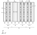
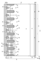
- FIG. 1 is a top view showing an example of a semiconductor device 100 according to one embodiment of the present invention
- FIG. 2 is an enlarged view of a region D in FIG. 1
- FIG. 3 is a diagram showing an example of an ee cross section in FIG. 2
- FIG. 10 is a diagram showing another example of the ee cross section
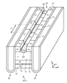
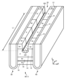
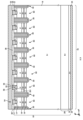
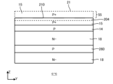
- 3 is a perspective cross-sectional view showing an example of a mesa portion 60 of a transistor portion 70
- FIG. FIG. 8 is a perspective cross-sectional view showing another example of the mesa portion 60-1 of the transistor portion 70
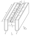
- 3 is a perspective cross-sectional view showing an example of a mesa portion 61 of a diode portion 80.
- FIG. 4 is a perspective cross-sectional view showing an example of a mesa portion 62 of a boundary portion 72;
- FIG. 3B shows an example of a YZ cross section along line aa shown in FIG. 3A.
- 3B shows another example of the YZ cross section taken along line aa shown in FIG. 3A.
- 3B shows an example of a YZ cross section taken along line bb shown in FIG. 3A.
- 3B shows an example of a YZ cross section along line cc shown in FIG. 3A.
- An XZ cross section of the mesa portion 60 in the vicinity of the trench contact portion 55 is shown.
- Another example of the XZ cross section in the vicinity of the trench contact portion 55 of the mesa portion 60 is shown.
- FIG. 8 is a diagram showing another example of the mesa portion 60 of the transistor portion 70.
- FIG. It is a view showing a YZ cross section of the mesa portion 60-2.
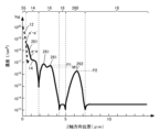
- FIG. 8 is a diagram showing an example of doping concentration distribution along the ff line of FIG. 7; It is a figure which shows the structural example of the trench contact part 55 in each mesa part. It is a figure which shows the structural example of the trench contact part 55 in each mesa part.
- 8 is a diagram showing another example of the mesa portion 60 of the transistor portion 70.
- FIG. FIG. 10 is a diagram showing another example of the mesa portion 60-3; 8 is a diagram showing another example of the mesa portion 61 of the diode portion 80.
- FIG. 8 is a diagram showing another example of the mesa portion 61 of the diode portion 80.
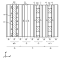
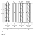
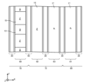
- FIG. FIG. 4 is a diagram showing an example of a combination of mesa portions in the semiconductor device 100; 4A and 4B are diagrams showing other examples of combinations of mesa portions in the semiconductor device 100; FIG. 4A and 4B are diagrams showing other examples of combinations of mesa portions in the semiconductor device 100; FIG. 4A and 4B are diagrams showing other examples of combinations of mesa portions in the semiconductor device 100; FIG. 4A and 4B are diagrams showing other examples of combinations of mesa portions in the semiconductor device 100; FIG. 4A and 4B are diagrams showing other examples of combinations of mesa portions in the semiconductor device 100; FIG. 4A and 4B are diagrams showing other examples of combinations of mesa portions in the semiconductor device 100; FIG.
- FIG. 3 is an ee cross section showing another configuration example of the semiconductor device 100.
- FIG. 3 is an ee cross section showing another configuration example of the semiconductor device 100.
- FIG. 3 is a top view showing another configuration example of the semiconductor device 100;
- FIG. 3 is a top view showing another configuration example of the semiconductor device 100;
- FIG. 3 is a top view showing another configuration example of the semiconductor device 100;
- FIG. 3 is a top view showing another configuration example of the semiconductor device 100;
- FIG. 3 is a top view showing another configuration example of the semiconductor device 100;
- FIG. 3 is a diagram showing another configuration example of the semiconductor device 100;
- FIG. 34 is a diagram showing an example of an ee cross section in FIG. 33; 3 is a diagram showing another configuration example of the semiconductor device 100;
- FIG. 35B is a diagram showing an example of the doping concentration distribution of the aa cross section and the a'-a' cross section in FIG. 35A;
- FIG. It shows an example in which a trench bottom region 260 is added to the structure of the mesa portion 60 shown in FIG. 7A. It shows an example in which a trench bottom region 260 is added to the structure of the mesa portion 61 shown in FIG. It shows an example in which a trench bottom region 260 is added to the structure of the mesa portion 62 shown in FIG. 3 is a diagram showing another configuration example of the semiconductor device 100;
- FIG. 35B is a diagram showing an example of the doping concentration distribution of the aa cross section and the a'-a' cross section in FIG. 35A;
- FIG. It shows an example in which a trench bottom region 260 is added to the structure
- one side in the direction parallel to the depth direction of the semiconductor substrate is called “upper”, and the other side is called “lower”.
- One of the two main surfaces of a substrate, layer or other member is called the upper surface and the other surface is called the lower surface.
- the directions of “up” and “down” are not limited to the direction of gravity or the direction when the semiconductor device is mounted.
- the Cartesian coordinate axes only specify the relative positions of the components and do not limit any particular orientation.
- the Z axis does not limit the height direction with respect to the ground.
- the +Z-axis direction and the ⁇ Z-axis direction are directions opposite to each other.
- the Z-axis direction is described without indicating positive or negative, it means a direction parallel to the +Z-axis and -Z-axis.
- orthogonal axes parallel to the upper and lower surfaces of the semiconductor substrate are defined as the X-axis and the Y-axis.
- the axis perpendicular to the upper and lower surfaces of the semiconductor substrate is defined as the Z-axis.
- the Z-axis direction may be referred to as the depth direction.
- a direction parallel to the upper and lower surfaces of the semiconductor substrate, including the X-axis and Y-axis may be referred to as a horizontal direction.
- the region from the center of the semiconductor substrate in the depth direction to the upper surface of the semiconductor substrate may be referred to as the upper surface side.
- the region from the center of the semiconductor substrate in the depth direction to the bottom surface of the semiconductor substrate may be referred to as the bottom surface side.
- the conductivity type of the doping region doped with impurities is described as P-type or N-type.
- impurities may specifically refer to either N-type donors or P-type acceptors, and may also be referred to as dopants.
- doping means introducing donors or acceptors into a semiconductor substrate to make it a semiconductor exhibiting N-type conductivity or a semiconductor exhibiting P-type conductivity.
- doping concentration means the concentration of donors or the concentration of acceptors at thermal equilibrium.
- the net doping concentration means the net concentration including charge polarity, where the donor concentration is the positive ion concentration and the acceptor concentration is the negative ion concentration.
- the donor concentration is N D and the acceptor concentration is N A , then the net net doping concentration at any location is N D ⁇ N A.
- net doping concentration may be simply referred to as doping concentration.
- a donor has the function of supplying electrons to a semiconductor.
- the acceptor has the function of receiving electrons from the semiconductor.
- Donors and acceptors are not limited to impurities per se.
- VOH defects in which vacancies (V), oxygen (O), and hydrogen (H) are combined in semiconductors function as donors that supply electrons.
- VOH defects are sometimes referred to herein as hydrogen donors.
- the semiconductor substrate herein is distributed throughout with N-type bulk donors.
- Bulk donors are donors from dopants that are substantially uniformly contained within the ingot during the manufacture of the ingot from which the semiconductor substrate is made.
- the bulk donor in this example is an element other than hydrogen.
- Bulk donor dopants include, but are not limited to, phosphorus, antimony, arsenic, selenium or sulfur.
- the bulk donor in this example is phosphorus.
- Bulk donors are also included in the P-type regions.
- the semiconductor substrate may be a wafer cut from a semiconductor ingot, or may be a chip obtained by singulating the wafer.
- Semiconductor ingots may be manufactured by any of the Czochralski method (CZ method), the magnetic field applied Czochralski method (MCZ method), and the float zone method (FZ method).
- the ingot in this example is manufactured by the MCZ method.
- the oxygen concentration contained in the substrate manufactured by the MCZ method is 1 ⁇ 10 17 to 7 ⁇ 10 17 /cm 3 .
- the oxygen concentration contained in the substrate manufactured by the FZ method is 1 ⁇ 10 15 to 5 ⁇ 10 16 /cm 3 .
- a higher oxygen concentration tends to generate hydrogen donors more easily.
- the bulk donor concentration may be the chemical concentration of bulk donors distributed throughout the semiconductor substrate and may be between 90% and 100% of the chemical concentration.
- a non-doped substrate that does not contain a dopant such as phosphorus may be used as the semiconductor substrate.
- the bulk donor concentration (D0) of the non-doped substrate is, for example, 1 ⁇ 10 10 /cm 3 or more and 5 ⁇ 10 12 /cm 3 or less.
- the bulk donor concentration (D0) of the non-doped substrate is preferably 1 ⁇ 10 11 /cm 3 or higher.
- the bulk donor concentration (D0) of the non-doped substrate is preferably 5 ⁇ 10 12 /cm 3 or less.
- Each concentration in the present invention may be a value at room temperature. As an example of the value at room temperature, the value at 300 K (Kelvin) (approximately 26.9° C.) may be used.
- references herein to P-type or N-type refer to higher doping concentrations than P-type or N-type; references to P-type or N-type refer to higher doping than P-type or N-type. It means that the concentration is low.
- P++ type or N++ type in this specification means that the doping concentration is higher than that of the P+ type or N+ type.
- the unit system in this specification is the SI unit system unless otherwise specified. The unit of length is sometimes displayed in cm, but various calculations may be performed after converting to meters (m).
- chemical concentration refers to the atomic density of impurities measured regardless of the state of electrical activation. Chemical concentrations can be measured, for example, by secondary ion mass spectroscopy (SIMS).
- the net doping concentrations mentioned above can be measured by the voltage-capacitance method (CV method).
- the carrier concentration measured by the spreading resistance measurement method (SR method) may be used as the net doping concentration.
- the carrier concentration measured by the CV method or SR method may be a value in thermal equilibrium.
- the donor concentration is sufficiently higher than the acceptor concentration in the N-type region, the carrier concentration in the region may be used as the donor concentration.
- the carrier concentration in that region may be used as the acceptor concentration.
- the doping concentration of the N-type regions is sometimes referred to herein as the donor concentration
- the doping concentration of the P-type regions is sometimes referred to as the acceptor concentration.
- the peak value may be taken as the concentration of donors, acceptors or net doping in the region.
- the average value of the concentration of donors, acceptors or net doping in the region may be used as the concentration of donors, acceptors or net doping.
- atoms/cm 3 or /cm 3 are used to express concentration per unit volume. This unit is used for donor or acceptor concentrations, or chemical concentrations, within a semiconductor substrate. The atoms notation may be omitted.
- the carrier concentration measured by the SR method may be lower than the donor or acceptor concentration.
- the carrier mobility of the semiconductor substrate may be lower than the value in the crystalline state. A decrease in carrier mobility is caused by scattering of carriers due to disorder of the crystal structure due to lattice defects or the like.
- the donor or acceptor concentration calculated from the carrier concentration measured by the CV method or the SR method may be lower than the chemical concentration of the element representing the donor or acceptor.
- the donor concentration of phosphorus or arsenic as a donor or the acceptor concentration of boron (boron) as an acceptor in a silicon semiconductor is about 99% of these chemical concentrations.
- the donor concentration of hydrogen serving as a donor in a silicon semiconductor is about 0.1% to 10% of the chemical concentration of hydrogen.
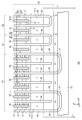
- FIG. 1 is a top view showing an example of a semiconductor device 100 according to one embodiment of the present invention.
- FIG. 1 shows the positions of each member projected onto the upper surface of the semiconductor substrate 10 .
- FIG. 1 only some members of the semiconductor device 100 are shown, and some members are omitted.
- a semiconductor device 100 includes a semiconductor substrate 10 .
- the semiconductor substrate 10 is a substrate made of a semiconductor material.
- the semiconductor substrate 10 is a silicon substrate.
- the semiconductor substrate 10 has an edge 162 when viewed from above. In this specification, simply referring to a top view means viewing from the top side of the semiconductor substrate 10 .
- the semiconductor substrate 10 of this example has two sets of edges 162 facing each other when viewed from above. In FIG. 1 , the X-axis and Y-axis are parallel to one of the edges 162 . Also, the Z-axis is perpendicular to the upper surface of the semiconductor substrate 10 .
- An active portion 160 is provided on the semiconductor substrate 10 .
- the active portion 160 is a region through which a main current flows in the depth direction between the upper and lower surfaces of the semiconductor substrate 10 when the semiconductor device 100 operates.
- An emitter electrode is provided above the active portion 160, but is omitted in FIG.
- the active portion 160 may refer to a region overlapping the emitter electrode when viewed from above. Also, the active portion 160 may include a region sandwiched between the active portions 160 when viewed from above.
- the active section 160 is provided with a transistor section 70 including transistor elements such as IGBTs.
- the active portion 160 may further include a diode portion 80 including a diode element such as a freewheeling diode (FWD).
- FWD freewheeling diode
- the transistor portions 70 and the diode portions 80 are alternately arranged along a predetermined arrangement direction (X-axis direction in this example) on the upper surface of the semiconductor substrate 10 .
- the semiconductor device 100 of this example is a reverse conducting IGBT (RC-IGBT).
- the region where the transistor section 70 is arranged is denoted by the symbol "I”
- the region where the diode section 80 is arranged is denoted by the symbol "F”.
- the direction perpendicular to the arrangement direction in top view may be referred to as the stretching direction (the Y-axis direction in FIG. 1).
- the transistor section 70 and the diode section 80 may each have a length in the extending direction. That is, the length in the Y-axis direction of the transistor section 70 is greater than the width in the X-axis direction. Similarly, the length in the Y-axis direction of the diode section 80 is greater than the width in the X-axis direction.
- the extending direction of the transistor portion 70 and the diode portion 80 may be the same as the longitudinal direction of each trench portion.
- the diode section 80 has an N+ type cathode region in a region in contact with the lower surface of the semiconductor substrate 10 .
- the region provided with the cathode region is referred to as the diode section 80 . That is, the diode portion 80 is a region that overlaps with the cathode region when viewed from above.
- a P + -type collector region may be provided in a region other than the cathode region on the lower surface of the semiconductor substrate 10 .
- the diode section 80 may also include an extension region 81 extending in the Y-axis direction from the diode section 80 to the gate wiring described later.
- a collector region is provided on the lower surface of the extension region 81 .
- the transistor section 70 has a P+ type collector region in a region in contact with the lower surface of the semiconductor substrate 10 .
- a gate structure having an N-type emitter region, a P-type base region, a gate conductive portion, and a gate insulating film is periodically arranged on the upper surface side of the semiconductor substrate 10 .
- the semiconductor device 100 may have one or more pads above the semiconductor substrate 10 .
- the semiconductor device 100 of this example has a gate pad 164 .
- Semiconductor device 100 may have pads such as an anode pad, a cathode pad, and a current sensing pad. Each pad is arranged near the edge 162 .
- the vicinity of the edge 162 refers to a region between the edge 162 and the emitter electrode in top view.
- each pad may be connected to an external circuit via a wiring such as a wire.
- a gate potential is applied to the gate pad 164 .
- Gate pad 164 is electrically connected to the conductive portion of the gate trench portion of active portion 160 .
- the semiconductor device 100 includes a gate wiring that connects the gate pad 164 and the gate trench portion. In FIG. 1, the gate wiring is hatched with oblique lines.
- the gate wiring of this example has a peripheral gate wiring 130 and an active side gate wiring 131 .
- the peripheral gate wiring 130 is arranged between the active portion 160 and the edge 162 of the semiconductor substrate 10 when viewed from above.
- the peripheral gate wiring 130 of this example surrounds the active portion 160 when viewed from above.
- a region surrounded by the peripheral gate wiring 130 in a top view may be the active portion 160 .
- a well region is formed below the gate wiring.
- a well region is a P-type region having a higher concentration than a base region, which will be described later, and is formed from the upper surface of the semiconductor substrate 10 to a position deeper than the base region.
- a region surrounded by the well region in top view may be the active portion 160 .
- the peripheral gate wiring 130 is connected to the gate pad 164 .
- the peripheral gate wiring 130 is arranged above the semiconductor substrate 10 .
- the peripheral gate wiring 130 may be a metal wiring containing aluminum or the like.
- the active side gate wiring 131 is provided in the active portion 160 .
- variations in wiring length from the gate pad 164 can be reduced for each region of the semiconductor substrate 10 .
- the peripheral gate wiring 130 and the active side gate wiring 131 are connected to the gate trench portion of the active portion 160 .
- the peripheral gate wiring 130 and the active side gate wiring 131 are arranged above the semiconductor substrate 10 .
- the peripheral gate wiring 130 and the active side gate wiring 131 may be wirings formed of a semiconductor such as polysilicon doped with impurities.
- the active side gate wiring 131 may be connected to the peripheral gate wiring 130 .
- the active-side gate wiring 131 of this example extends in the X-axis direction from one outer peripheral gate wiring 130 sandwiching the active portion 160 to the other outer peripheral gate wiring 130 so as to cross the active portion 160 at substantially the center in the Y-axis direction. is provided.
- the transistor portions 70 and the diode portions 80 may be alternately arranged in the X-axis direction in each divided region.
- the semiconductor device 100 also includes a temperature sensing portion (not shown), which is a PN junction diode made of polysilicon or the like, and a current detecting portion (not shown) that simulates the operation of the transistor portion provided in the active portion 160. good too.
- a temperature sensing portion which is a PN junction diode made of polysilicon or the like
- a current detecting portion (not shown) that simulates the operation of the transistor portion provided in the active portion 160. good too.
- the semiconductor device 100 of this example includes an edge termination structure portion 90 between the active portion 160 and the edge 162 when viewed from above.
- the edge termination structure 90 in this example is located between the peripheral gate line 130 and the edge 162 .
- the edge termination structure 90 reduces electric field concentration on the upper surface side of the semiconductor substrate 10 .
- Edge termination structure 90 may include at least one of a guard ring, a field plate, and a resurf annularly surrounding active portion 160 .
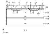
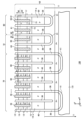
- FIG. 2 is an enlarged view of area D in FIG.
- Region D is a region including transistor section 70 , diode section 80 , and active-side gate wiring 131 .
- a boundary portion 72 may be provided between the transistor portion 70 and the diode portion 80 .
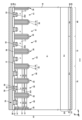
- the semiconductor device 100 of this example includes a gate trench portion 40 , a dummy trench portion 30 , a well region 11 , an emitter region 12 , a base region 14 and a contact region 15 provided inside the upper surface side of the semiconductor substrate 10 .
- Each of the gate trench portion 40 and the dummy trench portion 30 is an example of the trench portion.
- the semiconductor device 100 of this example also includes an emitter electrode 52 and an active-side gate wiring 131 provided above the upper surface of the semiconductor substrate 10 . Emitter electrode 52 and active-side gate line 131 are provided separately from each other.
- An interlayer insulating film is provided between the emitter electrode 52 and the active-side gate wiring 131 and the upper surface of the semiconductor substrate 10, but is omitted in FIG.
- a contact hole is provided through the interlayer insulating film of this example.
- a conductive member such as the emitter electrode 52 may be provided inside the contact hole.
- a trench contact portion 55 is provided on the upper surface of the semiconductor substrate 10 of this example.
- the trench contact portion 55 is a member in which a groove-like structure provided to a predetermined depth from the upper surface of the semiconductor substrate 10 is filled with a conductive material.
- the inside of the trench of the trench contact portion 55 is filled with a conductive material such as tungsten.
- a barrier metal containing at least one of a titanium film and a titanium nitride film may be provided between the conductive member and the semiconductor substrate 10 inside the trench of the trench contact portion 55 .
- the trench contact portion 55 is provided extending in the extension direction (Y-axis direction).
- the trench contact portion 55 is arranged below the contact hole of the interlayer insulating film described above.
- Emitter electrode 52 may be connected to semiconductor substrate 10 via a contact hole in the interlayer insulating film and trench contact portion 55 . In FIG. 2, each trench contact portion 55 is hatched with oblique lines.
- the emitter electrode 52 is provided above the gate trench portion 40 , the dummy trench portion 30 , the well region 11 , the emitter region 12 , the base region 14 and the contact region 15 .
- Emitter electrode 52 contacts at least part of well region 11 , emitter region 12 , contact region 15 , anode region 17 and base region 14 on the upper surface of semiconductor substrate 10 through contact hole and trench contact portion 55 .
- the emitter electrode 52 is connected to the dummy conductive portion in the dummy trench portion 30 through a contact hole provided in the interlayer insulating film.
- the emitter electrode 52 may be connected to the dummy conductive portion of the dummy trench portion 30 at the tip of the dummy trench portion 30 in the Y-axis direction.
- the active-side gate wiring 131 is connected to the gate trench portion 40 through a contact hole provided in the interlayer insulating film.
- the active-side gate wiring 131 may be connected to the gate conductive portion of the gate trench portion 40 at the tip portion 41 of the gate trench portion 40 in the Y-axis direction.
- the active-side gate wiring 131 is not connected to the dummy conductive portion within the dummy trench portion 30 .
- the emitter electrode 52 is made of a material containing metal.
- FIG. 2 shows the range in which the emitter electrode 52 is provided.
- the emitter electrode 52 is made of aluminum or a metal alloy such as an aluminum-silicon alloy such as AlSi, AlSiCu.
- the emitter electrode 52 may have a barrier metal made of titanium, a titanium compound, or the like under the region made of aluminum or the like. Further, the contact hole may have a plug formed by embedding tungsten or the like so as to be in contact with the barrier metal and the aluminum or the like.
- the well region 11 is provided so as to overlap with the active side gate wiring 131 .
- the well region 11 is also provided extending with a predetermined width in a range not overlapping the active side gate wiring 131 .
- the well region 11 of this example is provided away from the Y-axis direction end of the contact hole on the active side gate wiring 131 side.
- the well region 11 is a second conductivity type region having a higher doping concentration than the base region 14 .
- the base region 14 in this example is of P type and the well region 11 is of P+ type.
- Each of the transistor section 70, the boundary section 72 and the diode section 80 has one or more trench sections arranged in the arrangement direction.
- one or more gate trench sections 40 and one or more dummy trench sections 30 are alternately provided along the arrangement direction.
- a plurality of dummy trench portions 30 are provided along the array direction in the diode portion 80 of this example.
- the gate trench portion 40 is not provided in the diode portion 80 of this example.
- One or more dummy trench portions 30 are provided in the boundary portion 72 of this example along the arrangement direction.
- a gate trench portion 40 may be further provided in the boundary portion 72 .
- the gate trench portion 40 of this example connects the two straight portions 39 extending along the extending direction perpendicular to the arrangement direction (the portion of the trench that is linear along the extending direction) and the two straight portions 39 . It may have a tip 41 .
- the stretching direction in FIG. 2 is the Y-axis direction.
- At least a portion of the tip portion 41 is preferably provided in a curved shape when viewed from above.
- the dummy trench portions 30 are provided between the respective straight portions 39 of the gate trench portions 40 .
- One dummy trench portion 30 may be provided between the straight portions 39, or a plurality of dummy trench portions 30 may be provided.
- the dummy trench portion 30 may have a linear shape extending in the extending direction, and may have a linear portion 29 and a tip portion 31 like the gate trench portion 40 .
- the semiconductor device 100 shown in FIG. 2 includes both linear dummy trench portions 30 without tip portions 31 and dummy trench portions 30 with tip portions 31 .
- the diffusion depth of the well region 11 may be deeper than the depths of the gate trench portion 40 and the dummy trench portion 30 .
- Y-axis direction ends of the gate trench portion 40 and the dummy trench portion 30 are provided in the well region 11 when viewed from above. That is, the bottom of each trench in the depth direction is covered with the well region 11 at the end of each trench in the Y-axis direction. As a result, electric field concentration at the bottom of each trench can be relaxed.
- a mesa portion is provided between each trench portion in the arrangement direction.
- the mesa portion refers to a region sandwiched between trench portions inside the semiconductor substrate 10 .
- the upper end of the mesa portion is the upper surface of the semiconductor substrate 10 .
- the depth position of the lower end of the mesa portion is the same as the depth position of the lower end of the trench portion.
- the mesa portion of this example extends in the extension direction (Y-axis direction) along the trench on the upper surface of the semiconductor substrate 10 .
- the transistor portion 70 is provided with a mesa portion 60
- the diode portion 80 is provided with a mesa portion 61
- the boundary portion 72 is provided with a mesa portion 62 and a mesa portion 63 .
- the mesa portion 62 is the mesa portion closest to the transistor portion 70 at the boundary portion 72
- the mesa portion 63 is the mesa portion closest to the diode portion 80 at the boundary portion 72 .
- One or more mesas 62 may be further provided between the mesas 62 and 63
- One or more mesas 63 may be further provided between the mesas 62 and 63 .
- a mesa portion it refers to the mesa portion 60, the mesa portion 61, the mesa portion 62, and the mesa portion 63, respectively.
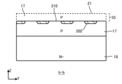
- a base region 14 is provided in each mesa portion. Of the base regions 14 exposed on the upper surface of the semiconductor substrate 10 in the mesa portion, the region arranged closest to the active-side gate wiring 131 is referred to as a base region 14-e. Although FIG. 2 shows the base region 14-e arranged at one end in the extending direction of each mesa, the base region 14-e is also arranged at the other end of each mesa. It is Each mesa portion has at least one of the first conductive type emitter region 12, the second conductive type contact region 15 and the second conductive type anode region 17 in the region sandwiched between the base regions 14-e when viewed from above. Either may be provided.
- the emitter region 12 in this example is of N+ type, the contact region 15 is of P+ type, and the anode region 17 is of P type.
- Emitter region 12 and contact region 15 may be provided between base region 14 and the upper surface of semiconductor substrate 10 in the depth direction.
- Anode region 17 may be provided at the same depth range as base region 14 .
- Anode region 17 may have the same doping concentration as base region 14 or may have a lower doping concentration than base region 14 .
- the mesa portion 60 of the transistor portion 70 has the emitter region 12 exposed on the upper surface of the semiconductor substrate 10 .
- the emitter region 12 is provided in contact with the gate trench portion 40 .
- the mesa portion 60 in contact with the gate trench portion 40 may be provided with the contact region 15 exposed to the upper surface of the semiconductor substrate 10 .
- Each of the contact region 15 and the emitter region 12 in the mesa portion 60 is provided from one trench portion to the other trench portion in the X-axis direction.
- the contact regions 15 and the emitter regions 12 of the mesa portion 60 are alternately arranged along the extension direction (Y-axis direction) of the trench portion.
- the contact regions 15 and the emitter regions 12 of the mesa portion 60 may be provided in stripes along the extending direction (Y-axis direction) of the trench portion.
- an emitter region 12 is provided in a region in contact with the trench portion, and a contact region 15 is provided in a region sandwiched between the emitter regions 12 .
- the mesa portion 61 of the diode portion 80 is not provided with the emitter region 12 .
- a base region 14 , an anode region 17 and a contact region 15 may be provided on the upper surface of the mesa portion 61 .
- a contact region 15 may be provided in a region sandwiched between the base regions 14-e on the upper surface of the mesa portion 61 so as to be in contact with each base region 14-e.
- An anode region 17 may be provided in a region sandwiched between the contact regions 15 on the upper surface of the mesa portion 61 .
- the anode region 17 may be arranged over the entire region sandwiched between the contact regions 15 .
- a contact region 15 may be provided on the upper surface of the mesa portion 62 of the boundary portion 72 .
- the contact region 15 is the entire region sandwiched between the base regions 14 - e on the upper surface of the mesa portion 61 .
- the emitter region 12 is not provided in the mesa portion 63 of the boundary portion 72 .
- a base region 14 , an anode region 17 and a contact region 15 may be provided on the upper surface of the mesa portion 63 .
- a contact region 15 may be provided in a region sandwiched between the base regions 14-e on the upper surface of the mesa portion 63 so as to be in contact with each base region 14-e.
- An anode region 17 may be provided in a region sandwiched between the contact regions 15 on the upper surface of the mesa portion 63 .
- the anode region 17 may be arranged over the entire region sandwiched between the contact regions 15 .
- the structures of the mesa portion 61 and the mesa portion 63 are the same.
- mesa portion 63 may have a different structure than mesa portion 61 .
- a trench contact portion 55 is provided in each mesa portion.
- a contact hole is provided in the interlayer insulating film above the trench contact portion 55 .
- the trench contact portion 55 is arranged in a region sandwiched between the base regions 14-e.
- the trench contact portion 55 of this example is provided above each region of the contact region 15 , the base region 14 , the anode region 17 and the emitter region 12 .
- Trench contact portion 55 is not provided in a region corresponding to base region 14 - e and well region 11 .
- the trench contact portion 55 may be arranged at the center in the arrangement direction (X-axis direction) of each mesa portion.
- an N+ type cathode region 82 is provided in a region in contact with the lower surface of the semiconductor substrate 10 .
- a P + -type collector region 22 may be provided in a region of the lower surface of the semiconductor substrate 10 where the cathode region 82 is not provided.
- a collector region 22 is provided in a region in contact with the lower surface of semiconductor substrate 10 in transistor portion 70 and boundary portion 72 . In FIG. 2, the boundary between cathode region 82 and collector region 22 is indicated by a dotted line.
- the cathode region 82 is arranged apart from the well region 11 in the Y-axis direction. As a result, the distance between the P-type region (well region 11), which has a relatively high doping concentration and is formed to a deep position, and the cathode region 82 can be secured, and the withstand voltage can be improved.
- the ends of the cathode regions 82 in the Y-axis direction in this example are arranged farther from the well region 11 than the ends of the trench contact portions 55 in the Y-axis direction.
- the end of the cathode region 82 in the Y-axis direction may be arranged between the well region 11 and the trench contact portion 55 .
- FIG. 3A is a diagram showing an example of the ee cross section in FIG.
- the ee section is the XZ plane passing through emitter region 12 and cathode region 82 .
- the semiconductor device 100 of this example has a semiconductor substrate 10, an interlayer insulating film 38, an emitter electrode 52 and a collector electrode 24 in the cross section.
- the interlayer insulating film 38 is provided on the upper surface of the semiconductor substrate 10 .
- the interlayer insulating film 38 is a film including at least one layer of an insulating film such as silicate glass doped with an impurity such as boron or phosphorus, a thermal oxide film, and other insulating films.
- the contact hole 54 described with reference to FIG. 2 is provided in the interlayer insulating film 38 .
- the emitter electrode 52 is provided above the interlayer insulating film 38 .
- Emitter electrode 52 is connected to semiconductor substrate 10 through contact hole 54 in interlayer insulating film 38 .
- the contact hole 54 may be filled with the same conductive material as the emitter electrode 52 above the interlayer insulating film 38, or may be filled with a different conductive material.
- a collector electrode 24 is provided on the lower surface 23 of the semiconductor substrate 10 .
- Emitter electrode 52 and collector electrode 24 are made of a metal material such as aluminum.
- the inside of the contact hole 54 may be filled with tungsten or the like.
- the direction (Z-axis direction) connecting the emitter electrode 52 and the collector electrode 24 is referred to as the depth direction.
- the semiconductor substrate 10 has an N-type or N ⁇ type drift region 18 .
- Drift region 18 is provided in each of transistor section 70 , boundary section 72 and diode section 80 .
- an N+ type emitter region 12 and a P type base region 14 are provided in order from the upper surface 21 side of the semiconductor substrate 10 .
- a drift region 18 is provided below the base region 14 .
- the mesa portion 60 may be provided with an N+ type accumulation region 16 .
- Accumulation region 16 is disposed between base region 14 and drift region 18 .
- the emitter region 12 is exposed on the upper surface 21 of the semiconductor substrate 10 and provided in contact with the gate trench portion 40 .
- the emitter region 12 may be in contact with trench portions on both sides of the mesa portion 60 .
- Emitter region 12 has a higher doping concentration than drift region 18 .
- the base region 14 is provided below the emitter region 12 .
- the base region 14 in this example is provided in contact with the emitter region 12 .
- the base region 14 may contact trench portions on both sides of the mesa portion 60 .
- the accumulation region 16 is provided below the base region 14 .
- the accumulation region 16 is an N+ type region with a higher doping concentration than the drift region 18 . That is, the accumulation region 16 has a higher donor concentration than the drift region 18 .
- the carrier injection promoting effect IE effect
- the accumulation region 16 may be provided so as to cover the entire bottom surface of the base region 14 in each mesa portion 60 .
- the mesa portion 60 may be provided with two or more accumulation regions 16 in the depth direction. Each accumulation region 16 has a doping concentration peak in the depth direction. Between the two accumulation regions 16 there is a trough of doping concentration in the depth direction. That is, mesa portion 60 may have more than one doping concentration peak from base region 14 toward drift region 18 .
- a drift region 18 may be provided between the accumulation region 16 and the base region 14, and the accumulation region 16 and the base region 14 may be in contact.
- the boundary portion 72 and the diode portion 80 may or may not be provided with the accumulation region 16 . In this example, neither the boundary portion 72 nor the diode portion 80 is provided with the accumulation region 16 .
- a P-type anode region 17 is provided in the mesa portion 61 of the diode portion 80 in contact with the upper surface 21 of the semiconductor substrate 10 .
- a drift region 18 is provided below the anode region 17 .
- the anode region 17 may have the same doping concentration as the base region 14 or may have a lower doping concentration than the base region 14. . By reducing the concentration of the anode region 17, it is possible to suppress hole injection in the mesa portion 61 and reduce the reverse recovery loss.
- a P+ type contact region 15 is provided in the mesa portion 62 of the boundary portion 72 so as to be in contact with the upper surface 21 of the semiconductor substrate 10 .
- Base region 14 or anode region 17 may be provided between contact region 15 and drift region 18 , and contact region 15 and drift region 18 may be in contact.
- a P-type anode region 17 is provided in the mesa portion 63 of the boundary portion 72 so as to be in contact with the upper surface 21 of the semiconductor substrate 10 .
- a drift region 18 is provided below the anode region 17 .
- An N+ type buffer region 20 may be provided under the drift region 18 in each of the transistor section 70 , the boundary section 72 and the diode section 80 .
- the doping concentration of buffer region 20 is higher than the doping concentration of drift region 18 .
- Buffer region 20 may have a concentration peak with a higher doping concentration than drift region 18 .
- the doping concentration of the concentration peak refers to the doping concentration at the apex of the concentration peak.
- an average value of doping concentrations in a region where the doping concentration distribution is substantially flat may be used as the doping concentration of the drift region 18.
- the buffer region 20 may have two or more concentration peaks in the depth direction (Z-axis direction) of the semiconductor substrate 10 .
- the concentration peak of the buffer region 20 may be provided at the same depth position as the chemical concentration peak of hydrogen (protons) or phosphorus, for example.
- Buffer region 20 may function as a field stop layer that prevents a depletion layer extending from the bottom edge of base region 14 from reaching P + -type collector region 22 and N + -type cathode region 82 .
- a P+ type collector region 22 is provided below the buffer region 20 in the transistor portion 70 and the boundary portion 72 .
- the doping concentration of collector region 22 is higher than the doping concentration of base region 14 .
- Collector region 22 may contain the same acceptor as base region 14 or may contain a different acceptor.
- the acceptor of the collector region 22 is boron, for example.
- An N+ type cathode region 82 is provided under the buffer region 20 in the diode section 80 .
- the doping concentration of cathode region 82 is higher than the doping concentration of drift region 18 .
- the donor for cathode region 82 is, for example, hydrogen or phosphorus. Note that the elements that serve as donors and acceptors in each region are not limited to the above examples.
- Collector region 22 and cathode region 82 are exposed at lower surface 23 of semiconductor substrate 10 and connected to collector electrode 24 .
- Collector electrode 24 may contact the entire bottom surface 23 of semiconductor substrate 10 .
- Emitter electrode 52 and collector electrode 24 are made of a metal material such as aluminum.
- part of the cathode region 82 may be replaced with a P-type region.
- the P-type region is sandwiched between cathode regions 82 .
- the P-type region may be sandwiched between the cathode regions 82 in the Y-axis direction.
- One or more gate trench portions 40 and one or more dummy trench portions 30 are provided on the upper surface 21 side of the semiconductor substrate 10 .
- Each trench portion extends from the upper surface 21 of the semiconductor substrate 10 through the base region 14 to below the base region 14 .
- the contact region 15 and/or the storage region 16 are provided, each trench section also passes through these doping regions.
- the fact that the trench penetrates the doping region is not limited to the order of forming the doping region and then forming the trench.
- a structure in which a doping region is formed between the trench portions after the trench portions are formed is also included in the structure in which the trench portion penetrates the doping regions.
- the transistor section 70 is provided with the gate trench section 40 and the dummy trench section 30 .
- a dummy trench portion 30 is provided in the boundary portion 72 .
- a gate trench portion 40 may be further provided in the boundary portion 72 .
- the diode section 80 is provided with the dummy trench section 30 and is not provided with the gate trench section 40 .
- the boundary between the collector region 22 and the cathode region 82 may be the boundary between the boundary portion 72 and the diode portion 80 in the X-axis direction. If the boundary portion 72 is not provided, the boundary between the collector region 22 and the cathode region 82 may be used as the boundary between the transistor portion 70 and the diode portion 80 in the X-axis direction. Further, among the trench portions in contact with the emitter region 12 , the trench portion closest to the diode portion 80 may be used as the boundary between the transistor portion 70 and the boundary portion 72 .
- the gate trench portion 40 has a gate trench provided in the upper surface 21 of the semiconductor substrate 10, a gate insulating film 42 and a gate conductive portion 44.
- a gate insulating film 42 is provided to cover the inner wall of the gate trench.
- the gate insulating film 42 may be formed by oxidizing or nitriding the semiconductor on the inner wall of the gate trench.
- the gate conductive portion 44 is provided inside the gate insulating film 42 inside the gate trench. That is, the gate insulating film 42 insulates the gate conductive portion 44 and the semiconductor substrate 10 from each other.
- the gate conductive portion 44 is formed of a conductive material such as polysilicon.
- the gate conductive portion 44 may be provided longer than the base region 14 in the depth direction.
- the gate trench portion 40 in the cross section is covered with the interlayer insulating film 38 on the upper surface 21 of the semiconductor substrate 10 .
- the gate conductive portion 44 is electrically connected to the gate wiring. When a predetermined gate voltage is applied to the gate conductive portion 44 , a channel is formed by an electron inversion layer in the surface layer of the interface contacting the gate trench portion 40 in the base region 14 .
- the dummy trench portion 30 may have the same structure as the gate trench portion 40 in the cross section.
- the dummy trench section 30 has a dummy trench provided in the upper surface 21 of the semiconductor substrate 10 , a dummy insulating film 32 and a dummy conductive section 34 .
- the dummy conductive portion 34 is electrically connected to the emitter electrode 52 .
- a dummy insulating film 32 is provided to cover the inner wall of the dummy trench.
- the dummy conductive portion 34 is provided inside the dummy trench and inside the dummy insulating film 32 .
- the dummy insulating film 32 insulates the dummy conductive portion 34 from the semiconductor substrate 10 .
- the dummy conductive portion 34 may be made of the same material as the gate conductive portion 44 .
- the dummy conductive portion 34 is made of a conductive material such as polysilicon.
- the dummy conductive portion 34 may have the same length as the gate conductive portion 44 in the depth direction.
- the gate trench portion 40 and the dummy trench portion 30 of this example are covered with an interlayer insulating film 38 on the upper surface 21 of the semiconductor substrate 10 .
- the bottoms of the dummy trench portion 30 and the gate trench portion 40 may be curved (curved in cross section) convex downward.
- At least one mesa portion 60 of the transistor portion 70 is provided with a trench contact portion 55 and a first bottom region 201 of the second conductivity type. All mesas 60 may be provided with trench contacts 55 and first bottom regions 201 .
- trench contact portion 55 is provided in the depth direction from upper surface 21 toward lower surface 23 of semiconductor substrate 10 .
- the trench contact portion 55 of this example is formed shallower than the lower end of the emitter region 12 .
- the trench contact portion 55 may be provided to the same depth as the bottom end of the emitter region 12 or may be formed deeper than the bottom end of the emitter region 12 .
- a plug 56 made of metal such as tungsten may be embedded in the trench contact portion 55 .
- the top surface 58 of the plug 56 may be the top surface 58 of the trench contact portion 55 .
- the top surface 58 of the plug 56 may be located on the emitter electrode 52 side (that is, above) the top surface 21 of the semiconductor substrate 10 .
- the trench contact portion 55 may be provided from the top surface 58 of the plug 56 to the bottom surface 23 side of the top surface 21 of the semiconductor substrate 10 .
- the upper surface 58 of the trench contact portion 55 may be positioned closer to the upper surface 21 than the upper surface of the interlayer insulating film 38 and may be positioned closer to the emitter electrode 52 than the upper surface 21 .
- the upper surface 58 of the trench contact portion 55 may be provided to the same depth position as the upper surface of the interlayer insulating film 38 .
- the first bottom region 201 in this example is a P+ type region with a higher doping concentration than the base region 14 .
- the first bottom region 201 is provided in contact with the bottom of the trench contact portion 55 .
- the first bottom region 201 connects with the base region 14 .
- At least part of the first bottom region 201 is provided below the emitter region 12 .
- the first bottom region 201 extends in the Y-axis direction along the trench contact portion 55 .
- the first bottom region 201 connects with the contact region 15 shown in FIG. According to this example, when the transistor portion 70 is turned off, holes directed from the lower surface 23 side toward the emitter region 12 can flow to the contact region 15 or the trench contact portion 55 through the first bottom region 201 . As a result, the resistance of the path through which holes pass can be reduced, and latch-up can be suppressed.
- At least one mesa portion 61 of the diode portion 80 is provided with a trench contact portion 55 and a second conductivity type second bottom region 202 . All mesas 61 may be provided with trench contacts 55 and second bottom regions 202 .
- the trench contact portion 55 of the diode portion 80 may have the same structure as the trench contact portion 55 of the transistor portion 70 .
- a lower end of the trench contact portion 55 of the diode portion 80 may be arranged inside the anode region 17 .
- the second bottom region 202 in this example is a P+ type region with a higher doping concentration than the anode region 17 and the base region 14 .
- the second bottom region 202 is provided in contact with the bottom of the trench contact portion 55 .
- a second bottom region 202 may be provided within the anode region 17 . That is, the second bottom region 202 does not have to contact the drift region 18 .
- the second bottom region 202 is provided extending in the Y-axis direction along the trench contact portion 55 .
- the length of the first bottom region 201 in the Y-axis direction is greater than the length of the second bottom region 202 in the Y-axis direction.
- a trench contact portion 55 is provided in the mesa portion 62 of the boundary portion 72 .
- the mesa portion 62 of the boundary portion 72 may be provided closest to the transistor portion 70 in the boundary portion 72 .
- the trench contact portion 55 of the mesa portion 62 may have the same structure as the trench contact portion 55 of the transistor portion 70 .
- a lower end of the trench contact portion 55 of the mesa portion 62 is arranged inside the contact region 15 .
- the lower end of trench contact portion 55 of mesa portion 62 is not provided with a P-type bottom region having a higher doping concentration than contact region 15 .
- a P-type bottom region 204 having a higher doping concentration than the contact region 15 may be provided at the lower end of the trench contact portion 55 of the mesa portion 62 .
- the dotted line indicates the position where the bottom region 204 is provided.
- the doping concentration of the contact region 15 the doping concentration of the upper surface 21 of the mesa portion 62 may be used.
- the mesa portion 63 of the boundary portion 72 is provided with the trench contact portion 55 and the third bottom region 203 of the second conductivity type.
- the mesa portion 63 of the boundary portion 72 may be provided closer to the diode portion 80 than the mesa portion 62 of the boundary portion 72 .
- All mesas 63 may be provided with trench contacts 55 and third bottom regions 203 .
- the trench contact portion 55 of the mesa portion 63 may have the same structure as the trench contact portion 55 of the transistor portion 70 .
- a lower end of the trench contact portion 55 of the mesa portion 63 may be arranged inside the anode region 17 .
- the third bottom region 203 in this example is a P+ type region with a higher doping concentration than the anode region 17 and the base region 14 .
- the third bottom region 203 is provided in contact with the bottom of the trench contact portion 55 .
- a third bottom region 203 may be provided inside the anode region 17 . That is, the third bottom region 203 does not have to be in contact with the drift region 18 .
- the third bottom region 203 is provided extending in the Y-axis direction along the trench contact portion 55 .
- the length of the first bottom region 201 in the Y-axis direction is greater than the length of the third bottom region 203 in the Y-axis direction.
- the third bottom region 203 By making the third bottom region 203 small, the injection amount of holes from the upper surface 21 side in the mesa portion 63 arranged near the diode portion 80 can be reduced. Therefore, the reverse recovery time of the diode section 80 can be shortened, and the reverse recovery loss can be reduced.
- the doping concentration, region size, shape and position on the Y-axis of the third bottom region 203 may be the same as the second bottom region 202 .
- the boundary portion 72 has one mesa portion 62 and one mesa portion 63 .
- boundary 72 may have multiple mesas 63 between mesas 62 and diodes 80 .
- the boundary portion 72 may have a plurality of mesa portions 62 between the mesa portion 63 and the transistor portion 70 .
- FIG. 3B is a diagram showing another example of the ee cross section.
- the trench contact portion 55 is formed deeper than in the example of FIG. 3A.
- Other structures may be similar to the semiconductor device 100 shown in FIG. 3A.
- the trench contact portion 55 is formed deeper than the emitter region 12 . That is, the trench contact portion 55 penetrates the emitter region 12 and the lower end of the trench contact portion 55 is arranged below the lower end of the emitter region 12 .
- a lower end of the trench contact portion 55 of the mesa portion 60 may be arranged at the same depth as the base region 14 .
- the trench contact portion 55 of another mesa portion may also have the same structure as the mesa portion 60 .
- the lower end of the trench contact portion 55 of the mesa portion 61 may be arranged at the same depth as the anode region 17 .
- the lower end of the trench contact portion 55 of the mesa portion 62 may be arranged at the same depth as the contact region 15 and may be arranged at the same depth as the base region 14 below the contact region 15 .
- a lower end of the trench contact portion 55 of the mesa portion 63 may be arranged at the same depth as the anode region 17 .
- the trench contact portion 55 of the other mesa portion may have the structure shown in FIG. 3A. That is, the trench contact portions 55 of other mesa portions may be formed shallower than the trench contact portions 55 of the mesa portion 60 .
- a bottom region (201, 202, 203 or 204) may be formed at the bottom of each trench contact portion 55, similar to the example of FIG. 3A.
- Bottom region 201 may be separate from emitter region 12 or may be in contact with emitter region 12 .
- the bottom edge of the bottom region 201 may be arranged at the same depth as the base region 14 .
- the lower ends of bottom region 202 and bottom region 203 may be arranged at the same depth as anode region 17 .
- the lower end of the bottom region 204 may be arranged at the same depth as the contact region 15 and may be arranged at the same depth as the base region 14 .
- FIG. 4A is a perspective cross-sectional view showing an example of the mesa portion 60 of the transistor portion 70.
- the mesa portion 60 shown in FIG. 4A may be referred to as a mesa portion 60-1.
- FIG. 4A shows the XZ cross section and top surface (XY plane) of the mesa portion 60-1, and side surfaces (XY plane) of the trench portion.
- the structure of the mesa portion 60-1 in the XZ cross section is the same as the mesa portion 60 shown in FIG. 3A.
- the structure of the mesa portion 60-1 on the upper surface is the same as that of the mesa portion 60 shown in FIG.
- the emitter regions 12 and the contact regions 15 are alternately arranged along the Y-axis direction on the upper surface of the mesa portion 60-1.
- a trench contact portion 55 is provided in the center of the mesa portion 60-1 in the X-axis direction. Note that FIG. 4A shows the groove structure of the trench contact portion 55 by omitting the metal inside the trench contact portion 55 .
- the first bottom region 201 extends in the Y-axis direction along the bottom surface of the trench contact portion 55 .
- the first bottom region 201 is hatched with oblique lines.
- the length L1 of the first bottom region 201 in the Y-axis direction may be the same as the length of the trench contact portion 55 in the Y-axis direction.
- the length L1 of the first bottom region 201 is the length of the first bottom regions 201 continuously provided along the Y-axis direction.
- the first bottom region 201 may be formed by implanting acceptor ions from the trench structure after forming the trench structure of the trench contact portion 55 and heat-treating the semiconductor substrate 10 . Since acceptor ions are diffused by heat treatment, the length L1 of the first bottom region 201 may be slightly larger than the length of the trench contact portion 55 in the Y-axis direction. The difference between the length L1 and the length of the trench contact portion 55 may be 10 ⁇ m or less, or may be 5 ⁇ m or less. Note that the length L ⁇ b>1 may be smaller than the length of the trench contact portion 55 . By masking part of the groove structure of the contact hole 54 or part of the groove structure of the trench contact portion 55 and implanting acceptor ions, the first bottom region 201 shorter than the trench contact portion 55 can be formed.
- the length L1 of the first bottom region 201 may be smaller than the length in the Y-axis direction of the nearest trench portion (the gate trench portion 40 or the dummy trench portion 30).
- the first bottom region 201 may be separate from the well region 11 shown in FIG.
- the width of the first bottom region 201 in the X-axis direction may be the same as the width of the bottom surface of the trench contact portion 55 or may be greater than the width of the bottom surface of the trench contact portion 55 .
- the bottom surface of the trench contact portion 55 may be the surface of the trench contact portion 55 that is formed closest to the lower surface 23 .
- the width of the first bottom region 201 in this example in the X-axis direction is greater than the width of the bottom surface of the trench contact portion 55 .
- the width of the first bottom region 201 in the X-axis direction is smaller than the width of the mesa portion 60 in the X-axis direction.
- the first bottom region 201 is provided apart from the trench portion.
- the first bottom region 201 may be exposed on the entire bottom surface of the trench contact portion 55 .
- the first bottom region 201 may also be exposed on part of the sidewalls of the trench structure of the trench contact portion 55 .
- FIG. 4B is a perspective cross-sectional view showing another example of the mesa portion 60-1 of the transistor portion 70.
- FIG. The structure of the mesa portion 60-1 in the XZ cross section of this example is the same as the mesa portion 60 shown in FIG. 3B.
- the structure of the mesa portion 60-1 on the upper surface is the same as that of the mesa portion 60 shown in FIG. That is, the mesa portion 60-1 of this example differs from the mesa portion 60-1 shown in FIG. 4A in that the trench contact portion 55 penetrates the emitter region 12.
- Other structures are similar to the example of FIG. 4A.
- FIG. 5 is a perspective cross-sectional view showing an example of the mesa portion 61 of the diode portion 80.
- the mesa portion 61 shown in FIG. 5 may be referred to as a mesa portion 61-1.
- FIG. 5 shows the XZ cross section and upper surface (XY plane) of the mesa portion 61-1, and side surfaces (XY plane) of the trench portion.
- the structure of the mesa portion 61-1 in the XZ cross section is the same as the mesa portion 61 shown in FIG. 3A.
- the structure of the mesa portion 61-1 on the upper surface is the same as that of the mesa portion 61 shown in FIG.
- the anode region 17 and the trench contact portion 55 are arranged on the upper surface of the mesa portion 61-1.
- the structure of the trench contact portion 55 is similar to the trench contact portion 55 of FIG. 4A.
- the second bottom region 202 is exposed at the bottom surface of the trench contact portion 55 as described above.
- the second bottom region 202 may also be exposed on part of the sidewalls of the trench structure of the trench contact portion 55 .
- the second bottom region 202 is hatched with oblique lines.
- the length L2 of the second bottom region 202 in the Y-axis direction is smaller than the length of the trench contact portion 55 in the Y-axis direction.
- a plurality of second bottom regions 202 are discretely arranged along the Y-axis direction.
- the plurality of second bottom regions 202 may be arranged at regular intervals in the Y-axis direction.
- the length L2 of the second bottom region 202 is the length of one second bottom region 202 continuously provided along the Y-axis direction.
- the trench contact portion 55 of the mesa portion 61-1 may be formed deeper like the trench contact portion 55 shown in FIG. 4B.
- the length L1 of the first bottom region 201 shown in FIG. 4A or 4B is greater than the length L2 of the second bottom region 202.
- injection of holes in the diode section 80 can be suppressed while suppressing latch-up in the transistor section 70 .
- the contact between the emitter electrode 52 and the anode region 17 in the diode portion 80 can be improved.
- the length L1 may be twice or more, five times or more, or ten times or more the length L2.
- the sum of the lengths L1 of the one or more first bottom regions 201 in one mesa portion 60 (referred to as the first sum) is the sum of the lengths L2 of the plurality of second bottom regions 202 in one mesa portion 61. greater than (referred to as the second sum).
- the first sum may be 1.5 times or more, 2 times or more, or 3 times or more the second sum.
- the total area (first total area) of the one or more first bottom regions 201 in one mesa portion 60 in top view is the total area (first total area) of the plurality of second bottom regions 202 in one mesa portion 61 in top view ( (referred to as the second total area).
- the first total area may be 1.5 times or more the second total area, may be 2 times or more, or may be 3 times or more.
- the second bottom region 202 may be formed in the same manner as the first bottom region 201. However, when forming the second bottom region 202 , acceptor ions are selectively implanted into the trench contact portion 55 . The second bottom region 202 may be separate from the well region 11 shown in FIG.
- the width of the second bottom region 202 in the X-axis direction may be the same as the width of the trench contact portion 55 or may be greater than the width of the trench contact portion 55 .
- the width of the second bottom region 202 in the X-axis direction is smaller than the width of the mesa portion 61 in the X-axis direction.
- a second bottom region 202 is provided separate from the trench portion.
- the width of the second bottom region 202 in the X-axis direction may be the same as or different from the width of the first bottom region 201 in the X-axis direction.
- the width of the second bottom region 202 in the X-axis direction may be smaller than the width of the first bottom region 201 in the X-axis direction. In this case, hole injection in the diode section 80 can be further suppressed.
- the doping concentration of the second bottom region 202 may be the same as or different from the doping concentration of the first bottom region 201 .
- the doping concentration of the second bottom region 202 may be lower than the doping concentration of the first bottom region 201 . In this case, hole injection in the diode section 80 can be further suppressed.
- the mesa portion 63 of the boundary portion 72 may have the same structure as the mesa portion 61 of the diode portion 80 .
- the mesa portion 63 has a third bottom region 203 instead of the second bottom region 202 in the mesa portion 61 .
- Other structures are the same as those of the mesa portion 61 .
- the shape, size and arrangement of the third bottom region 203 may be the same as those of the second bottom region 202 . That is, the length L1 of the first bottom region 201 in the Y-axis direction is greater than the length of the third bottom region 203 in the Y-axis stretching direction. Also, the length L2 of the second bottom region 202 in the Y-axis direction may be the same as the length of the third bottom region 203 in the Y-axis direction. In other examples, second bottom region 202 may be longer or shorter than third bottom region 203 .
- the doping concentration of the third bottom region 203 may be the same as or different from the doping concentration of the second bottom region 202 .
- At least one mesa portion 62 may not be provided with the third bottom region 203 .
- the third bottom region 203 may not be provided in the mesa portion 62 closest to the diode portion 80 . Since the cathode region 82 is not provided below the mesa portion 62 and does not function as the diode portion 80, the contact between the mesa portion 62 and the emitter electrode 52 may be low. Also, by omitting the third bottom region 203, the amount of hole injection in the vicinity of the diode portion 80 can be suppressed.
- FIG. 6 is a perspective sectional view showing an example of the mesa portion 62 of the boundary portion 72.
- FIG. FIG. 6 shows the XZ cross section and upper surface (XY plane) of the mesa portion 62 and side surfaces (XY plane) of the trench portion.
- the structure of the mesa portion 62 in the XZ cross section is the same as the mesa portion 62 shown in FIG. 3A.
- the structure of the mesa portion 62 on the upper surface is the same as that of the mesa portion 62 shown in FIG.
- a contact region 15 and a trench contact portion 55 are arranged on the upper surface of the mesa portion 62 .
- the structure of the trench contact portion 55 is similar to the trench contact portion 55 of FIG. 4A.
- the contact region 15 is exposed on the bottom and side surfaces of the trench contact portion 55 of the mesa portion 62 .
- the bottom region 204 is provided on the bottom surface of the trench contact portion 55 of the mesa portion 62
- the bottom region 204 is exposed on the bottom surface and side surfaces of the trench contact portion 55 of the mesa portion 62 .
- the trench contact portion 55 of the mesa portion 62 may be formed deeper like the trench contact portion 55 shown in FIG. 4B.
- FIG. 7A shows an example of a YZ cross section along line aa shown in FIG. 3A.
- 7A shows a cross section of the mesa portion 60 of the transistor portion 70.
- the cross section passes through the trench contact portion 55 .
- the emitter region 12 and the contact region 15 projected on the cross section are indicated by dashed lines.
- the contact regions 15 and the emitter regions 12 are alternately arranged in the Y-axis direction. Contact region 15 and emitter region 12 are formed to a predetermined depth from upper surface 21 of semiconductor substrate 10 . Contact region 15 may be formed below emitter region 12 .
- the first bottom region 201 connects two contact regions 15 spaced apart in the Y-axis direction.
- the first bottom region 201 may connect all contact regions 15 provided in the mesa 60 .
- the groove structure of the trench contact portion 55 may be formed after the emitter region 12 and the contact region 15 are formed on the upper surface 21 of the semiconductor substrate 10. Portions of emitter region 12 and contact region 15 are removed when forming the trench structure.
- the trench structure is preferably formed shallower than the lower end of contact region 15 . In other words, the contact region 15 remains below the trench structure.
- the groove structure may be formed shallower than the lower end of the emitter region 12 and may be formed deeper than the lower end of the emitter region 12 .
- the trench structure of the trench contact portion 55 is shallower than the lower edge of the emitter region 12. In the example of FIG. Thus, the emitter region 12 remains below the bottom surface 210 of the trench structure.
- acceptor ions are implanted from the bottom surface 210 of the trench structure to form the first bottom region 201 .
- the acceptor ions are implanted at a dose amount capable of inverting the emitter region 12 below the bottom surface 210 into a P-type region.
- the bottom of the emitter region 12 indicated by dashed lines in FIG. 7A corresponds to the bottom of the emitter region 12 before implanting acceptor ions.
- Acceptor ions may also be implanted into the region where the contact region 15 is formed. That is, the first bottom region 201 may be formed overlapping the contact region 15 .
- the overlapping portion of the first bottom region 201 and the contact region 15 has a higher doping concentration than the original contact region 15 because the doping concentrations of the respective regions overlap.
- the portion where the contact region 15 and the first bottom region 201 overlap is also referred to as the first bottom region 201 .
- the first bottom region 201 may alternately have a relatively high doping concentration portion and a relatively low doping concentration portion along the Y-axis direction.
- the doping concentration in the portion overlapping the contact region 15 is higher than the doping concentration in the portion overlapping the emitter region 12 .
- the first bottom region 201 may have a portion formed deeper than the emitter region 12 . At least a portion of the first bottom region 201 is provided closer to the upper surface 21 than the lower end 19 of the contact region 15 . In the example of FIG. 7A , the entire first bottom region 201 is located above the lower edge 19 of the contact region 15 . By protruding the contact region 15 downward, the holes attracted to the emitter region 12 can be easily extracted through the contact region 15 .
- hole carriers traveling from the drift region 18 toward the emitter region 12 can flow through the first bottom region 201 to the contact region 15 or the trench contact portion 55 . Therefore, latch-up of the transistor section 70 can be suppressed.
- FIG. 7B shows another example of the YZ cross section along line aa shown in FIG. 3A.
- the mesa portion 60-1 of this example differs from the mesa portion 60-1 shown in FIG. 7A in that the trench contact portion 55 penetrates the emitter region 12.
- the bottom region 201 is also provided at a deeper position than in the example of FIG. 7A.
- Other structures are similar to the example of FIG. 7A.
- the bottom region 201 of this example also connects two contact regions 15 adjacent in the Y-axis direction.
- the bottom region 201 may be separated from or in contact with the emitter region 12 in the Z-axis direction.
- FIG. 8 shows an example of a YZ cross section along line bb shown in FIG. 3A. 8 shows a cross section of the mesa portion 61 of the diode portion 80. FIG. The cross section passes through the trench contact portion 55 . In FIG. 8, the anode region 17 projected on the cross section is indicated by a dashed line.
- the second bottom regions 202 are discretely arranged along the Y-axis direction.
- the second bottom region 202 is formed from the bottom surface 210 of the trench contact portion 55 to a predetermined depth.
- the second bottom region 202 may be formed shallower than the lower end of the anode region 17 .
- the groove structure of the trench contact portion 55 may be formed after the anode region 17 is formed on the upper surface 21 of the semiconductor substrate 10.
- acceptor ions are implanted from the bottom surface 210 of the trench structure to form the second bottom region 202 .
- the first bottom region 201 and the second bottom region 202 may be formed in the same process.
- the dose per unit area of the first bottom region 201 and the second bottom region 202 may be the same.
- hole injection from the second bottom region 202 can be suppressed while ensuring contact between the emitter electrode 52 and the anode region 17 .
- the reverse recovery loss of the diode section 80 can be reduced.
- the trench contact portion 55 of the mesa portion 61 may be formed deeper like the trench contact portion 55 shown in FIG. 7B.
- FIG. 9 shows an example of a YZ cross section along line cc shown in FIG. 3A.
- FIG. 9 shows a cross section of the mesa portion 62 of the boundary portion 72 .
- the cross section passes through the trench contact portion 55 .
- the contact region 15 projected on the cross section is indicated by a dashed line.
- a bottom region having a concentration higher than that of the contact region 15 is not formed at the bottom of the trench contact portion 55 .
- the bottom region 204 is indicated by a dotted line when the bottom region 204 is provided on the bottom surface of the trench contact portion 55 of the mesa portion 62 .
- the trench contact portion 55 of the mesa portion 62 may be formed deeper like the trench contact portion 55 shown in FIG. 7B.
- FIG. 10A shows an XZ cross section of the mesa portion 60 in the vicinity of the trench contact portion 55.
- FIG. 10A the conductive material inside the trench contact portion 55 is omitted to show the trench structure.
- the lower end (bottom surface 210 ) of the trench contact portion 55 may be arranged closer to the upper surface 21 side of the semiconductor substrate 10 than the lower end 25 of the emitter region 12 .
- the bottom surface 210 of the trench contact portion 55 may be at the same depth position as the lower end 25 of the emitter region 12 and may be arranged closer to the lower surface 23 than the lower end 25 .
- the lower end 27 of the first bottom region 201 is arranged closer to the lower surface 23 than the lower end 25 of the emitter region 12 .
- a lower edge 27 of the first bottom region 201 may be located within the base region 14 .
- the first bottom region 201 may have a portion 220 located closer to the top surface 21 than the bottom surface 210 of the trench contact portion 55 .
- FIG. 10B shows another example of the XZ cross section in the vicinity of the trench contact portion 55 of the mesa portion 60.
- FIG. The mesa portion 60 of this example differs from the mesa portion 60 shown in FIG. 10A in that the trench contact portion 55 penetrates the emitter region 12 . That is, the bottom surface 210 of the trench contact portion 55 is formed deeper than the lower end 25 of the emitter region 12 . As the trench contact portion 55 is formed deeper, the bottom region 201 is also provided at a deeper position than in the example of FIG. 10A. Other structures are similar to the example of FIG. 10A.
- the bottom region 201 may be separated from or in contact with the emitter region 12 in the Z-axis direction.
- FIG. 11 is a diagram showing another example of the mesa portion 60 of the transistor portion 70.
- FIG. The mesa portion 60 shown in FIG. 11 is called a mesa portion 60-2.
- the mesa portion 60-2 of this example differs from the mesa portion 60-1 in the structure of the first bottom region 201.
- FIG. Other points are the same as the mesa portion 60-1.
- the mesa portion 60-2 has a plurality of first bottom regions 201 discretely arranged along the Y-axis direction.
- the first bottom region 201 of this example may be arranged between two contact regions 15 adjacent in the Y-axis direction.
- the contact region 15 may be exposed between two adjacent first bottom regions 201 on the bottom surface of the trench contact portion 55 .
- the trench contact portion 55 of the mesa portion 60-2 may pass through the emitter region 12, like the trench contact portion 55 shown in FIG. 4B.
- FIG. 12 is a diagram showing the YZ cross section of the mesa portion 60-2.
- the first bottom region 201 of this example connects two contact regions 15 adjacent in the Y-axis direction.
- the first bottom region 201 may or may not have a portion overlapping the contact region 15 .
- the trench contact portion 55 of the mesa portion 60-2 may pass through the emitter region 12, like the trench contact portion 55 shown in FIG. 7B.
- FIG. 13 is a diagram showing an example of doping concentration distribution along the ff line in FIG. 7A.
- Line ff is a line that passes through contact region 15 and first bottom region 201 of mesa 60-1.
- the position in the depth direction of the upper surface 21 of the semiconductor substrate 10 is Z21, and the position in the depth direction of the bottom surface 210 of the trench contact portion 55 is Z210. From position Z21 to position Z210 on the upper surface 21 in FIG. 13, the doping concentration distribution of the contact region 15 projected on the cross section of FIG. 7A is shown.
- the doping concentration distribution at positions deeper than the position Z210 in FIG. 13 is the distribution below the trench contact portion 55 .
- the doping concentration D1 (/cm 3 ) of the first bottom region 201 may be higher than the doping concentration D2 (/cm 3 ) of the contact region 15 .
- the doping concentration D1 of the first bottom region 201 may use the maximum doping concentration in the P-type regions between location Z210 and the N-type regions (eg, accumulation region 16 or drift region 18).
- the doping concentration at location Z210 may be the doping concentration D1 of the first bottom region 201 .
- the maximum value of the doping concentration in the P-type region from position Z21 to position Z210 may be set as the doping concentration D2 of the contact region 15.
- the doping concentration at the position Z21 may be the doping concentration D2 of the contact region 15.
- the doping concentration D1 may be two times or more, five times or more, or ten times or more the doping concentration D2. Increasing the doping concentration D1 makes it easier to suppress latch-up.
- the first bottom region 201 may have a first concentration peak 251 in the depth direction of the doping concentration.
- the first density peak 251 has a slope from the vertex toward the lower surface 23 side and does not have a slope toward the upper surface 21 side from the vertex.
- the contact region 15 may have a second concentration peak 252 in the depth direction of the doping concentration.
- the second density peak 252 has a slope from the vertex toward the lower surface 23 side and does not have a slope toward the upper surface 21 side from the vertex.
- the half width at half maximum HWHM1 of the first concentration peak 251 may be smaller than the half width at half maximum HWHM2 of the second concentration peak 252 .
- the half width at half maximum HWHM1 may be half or less, 1/4 or less, or 1/10 or less of the half width at half maximum HWHM2.
- the doping concentration D1 of the first concentration peak 251 can be increased without increasing the dose of acceptor ions for forming the first bottom region 201 .
- the half width at half maximum HWHM1 of the first concentration peak 251 can be controlled by the temperature or time of heat treatment after implanting acceptor ions to form the first bottom region 201 .
- FIG. 14 is a diagram showing a structural example of the trench contact portion 55 in each mesa portion.
- the trench contact portions 55-1, 55-2 and 55-3 of the mesa portions 60, 61 and 63 have different depths.
- the trench contact portion 55 in the mesa portion 62 may have the same structure as the trench contact portion 55 - 2 in the mesa portion 61 .
- W1 be the width in the X-axis direction of the trench contact portion 55-1 of the mesa portion 60
- Z1 be the depth in the Z-axis direction
- W2 be the width in the X-axis direction of the trench contact portion 55-2 of the mesa portion 61
- Z2 be the depth in the Z-axis direction
- W3 be the width in the X-axis direction of the trench contact portion 55-3 of the mesa portion 63
- Z3 be the depth in the Z-axis direction.
- width W1, width W2 and width W3 are the same.
- depth Z2 is greater than depth Z1. That is, the trench contact portion 55-2 is provided below the contact portion 55-1.
- the width of the bottom surface 210-2 of the trench contact portion 55-2 can be made smaller than the width of the bottom surface 210-1 of the trench contact portion 55-1. Therefore, the width in the X-axis direction of the second bottom region 202 provided at the bottom of the trench contact portion 55-2 is equal to the width in the X-axis direction of the first bottom region 201 provided at the bottom of the trench contact portion 55-1. By making it smaller than the width, injection of holes in the mesa portion 61 can be suppressed.
- the depth Z3 may be greater than the depth Z2. That is, the trench contact portion 55-3 is provided below the contact portion 55-2.
- the depth Z3 By making the depth Z3 larger than the depth Z2, the width in the X-axis direction of the bottom surface 210-3 of the trench contact portion 55-3 is equal to the width in the X-axis direction of the bottom surface 210-2 of the trench contact portion 55-2. can be smaller than For this reason, the third bottom region 203 provided at the bottom of the trench contact portion 55-3 is made smaller than the second bottom region 202 provided at the bottom of the trench contact portion 55-2. Pore injection can be suppressed.
- the depth Z3 may be 1.1 times or more, 1.2 times or more, or 1.5 times or more the depth Z2.
- the depth Z2 may be 1.1 times or more, 1.2 times or more, or 1.5 times or more the depth Z1.
- the trench contact portion 55 of the mesa portion 60 may pass through the emitter region 12, similar to the trench contact portion 55 shown in FIG. 4B.
- FIG. 15 is a diagram showing a structural example of the trench contact portion 55 in each mesa portion.
- the trench contact portions 55-1, 55-2 and 55-3 of the mesa portions 60, 61 and 63 have different widths in the X-axis direction.
- the trench contact portion 55 in the mesa portion 62 may have the same structure as the trench contact portion 55 - 2 in the mesa portion 61 .
- the width of the trench contact portion 55-1 of the mesa portion 60 in the X-axis direction is W1
- the width of the trench contact portion 55-2 of the mesa portion 61 in the X-axis direction is W2
- the width of the trench contact portion 55-3 of the mesa portion 63 is W2.
- W3 be the width in the axial direction.
- the width of each trench contact portion 55 - 1 is the width of the upper surface 21 of the semiconductor substrate 10 .
- the depth of each trench contact portion 55 may be the same.
- the depth of each trench contact portion 55 may be different.
- Each trench contact portion 55 may have the depth shown in FIG.
- the width W2 is smaller than the width W1.
- the width W2 smaller than the width W1
- the width of the bottom surface 210-2 of the trench contact portion 55-2 can be made smaller than the width of the bottom surface 210-1 of the trench contact portion 55-1. Therefore, the width in the X-axis direction of the second bottom region 202 provided at the bottom of the trench contact portion 55-2 is equal to the width in the X-axis direction of the first bottom region 201 provided at the bottom of the trench contact portion 55-1.
- injection of holes in the mesa portion 61 can be suppressed.
- the width W3 may be smaller than the width W2.
- the width W3 By making the width W3 smaller than the width W2, the width of the bottom surface 210-3 of the trench contact portion 55-3 can be made smaller than the width of the bottom surface 210-2 of the trench contact portion 55-2. Therefore, the width in the X-axis direction of the third bottom region 203 provided at the bottom of the trench contact portion 55-3 is equal to the width in the X-axis direction of the second bottom region 202 provided at the bottom of the trench contact portion 55-2. By making it smaller than the width, injection of holes in the mesa portion 63 can be suppressed.
- the width W1 may be 1.1 times or more, 1.2 times or more, or 1.5 times or more the width W2.
- the width W2 may be 1.1 times or more, 1.2 times or more, or 1.5 times or more the width W3.
- the trench contact portion 55 of the mesa portion 60 may pass through the emitter region 12, similar to the trench contact portion 55 shown in FIG. 4B.
- FIG. 16A is a diagram showing another example of the mesa portion 60 of the transistor portion 70.
- FIG. The mesa portion 60 shown in FIG. 16A is called a mesa portion 60-3.
- the mesa portion 60-3 of this example differs from the mesa portion 60-1 shown in FIG. 4A in that it has a base region 14 instead of the contact region 15.
- FIG. Other points are the same as the mesa portion 60-1 shown in FIG. 4A. According to this example as well, holes can be extracted via the first bottom region 201 and the trench contact portion 55, so latch-up of the transistor portion 70 can be suppressed.
- FIG. 16B is a diagram showing another example of the mesa portion 60-3.
- the mesa portion 60-3 of this example differs from the mesa portion 60-1 shown in FIG. 4B in that it has a base region 14 instead of the contact region 15.
- Other points are the same as the mesa portion 60-1 shown in FIG. 4B.
- holes can be extracted via the first bottom region 201 and the trench contact portion 55, so latch-up of the transistor portion 70 can be suppressed.
- FIG. 17 is a diagram showing another example of the mesa portion 61 of the diode portion 80.
- FIG. The mesa portion 61 shown in FIG. 17 is called a mesa portion 61-2.
- the mesa portion 61-2 of this example differs from the mesa portion 61-1 in that it has one second bottom region 202 formed continuously. Other points are the same as the mesa portion 61-1.
- the length L2 of the second bottom region 202 may be shorter than the length L1 of the first bottom region 201 . In other examples, the length L2 of the second bottom region 202 may be the same as the length L1 of the first bottom region 201 .
- the doping concentration of the second bottom region 202 may be lower than the doping concentration of the first bottom region 201 . In this case, even if the length L2 is the same as the length L1, the amount of holes injected into the mesa portion 61-2 can be suppressed.
- the doping concentration of the second bottom region 202 may be the same as the doping concentration of the first bottom region 201 .
- the trench contact portion 55 of the mesa portion 61-2 may be formed deeper like the trench contact portion 55 shown in FIG. 4B.
- FIG. 18 is a diagram showing another example of the mesa portion 61 of the diode portion 80.
- FIG. The mesa portion 61 shown in FIG. 18 is called a mesa portion 61-3.
- the mesa portion 61-3 of this example differs from the mesa portion 61-1 or 61-2 in that the emitter region 12 and the anode region 17 are alternately exposed along the Y-axis direction on the upper surface 21. .
- Other points are the same as the mesa portion 61-1 or the mesa portion 61-2.
- the transistor section 70 may have the mesa section 60 having any configuration described with reference to FIGS. 1 to 18 .
- the diode section 80 may have the mesa section 61 having any configuration described with reference to FIGS. 1 to 18 .
- Transistor portion 70 and diode portion 80 may have any combination of mesa portion 60 and mesa portion 61 described above.
- the trench contact portion 55 of the mesa portion 61-3 may be formed deeper like the trench contact portion 55 shown in FIG. 4B.
- FIG. 19 is a diagram showing an example of a combination of mesa portions in the semiconductor device 100.
- the transistor section 70 of this example has a mesa section 60-1.
- the diode section 80 has a mesa section 61-1.
- the structure of the mesa portion 63 is similar to that of the mesa portion 61-1.
- FIG. 20 is a diagram showing another example of a combination of mesa portions in the semiconductor device 100.
- the transistor section 70 of this example has a mesa section 60-2.
- the diode section 80 has a mesa section 61-1.
- the structure of the mesa portion 63 is similar to that of the mesa portion 61-1.
- FIG. 21 is a diagram showing another example of a combination of mesa portions in the semiconductor device 100.
- the transistor section 70 of this example has a mesa section 60-1.
- the diode section 80 has a mesa section 61-2.
- the structure of the mesa portion 63 is similar to that of the mesa portion 61-2.
- FIG. 22A and 22B are diagrams showing other examples of combinations of mesa portions in the semiconductor device 100.
- FIG. The transistor section 70 of this example has a mesa section 60-3.
- the diode section 80 has a mesa section 61-2.
- the structure of the mesa portion 63 is similar to that of the mesa portion 61-2.
- FIG. 23A and 23B are diagrams showing other examples of combinations of mesa portions in the semiconductor device 100.
- FIG. The transistor section 70 of this example has a mesa section 60-3.
- the diode portion 80 has a mesa portion 61-3.
- the structure of the mesa portion 63 is similar to that of the mesa portion 61-3.
- FIG. 24A and 24B are diagrams showing other examples of combinations of mesa portions in the semiconductor device 100.
- FIG. The transistor section 70 of this example has a mesa section 60-3.
- the diode portion 80 has a mesa portion 61-3.
- the structure of the mesa portion 63 is similar to that of the mesa portion 61-2.
- FIG. 25A and 25B are diagrams showing other examples of combinations of mesa portions in the semiconductor device 100.
- the transistor section 70 of this example has a mesa section 60-3.
- the diode section 80 has a mesa section 61-2.
- the structure of the mesa portion 63 is similar to that of the mesa portion 61-3.
- the combination of mesa portions in the semiconductor device 100 is not limited to the examples shown in FIGS. 19 to 25.
- FIG. 26 is an ee cross section showing another configuration example of the semiconductor device 100.
- FIG. The semiconductor device 100 of this example differs from the semiconductor device 100 described in FIGS. 1 to 25 in the structures of the boundary portion 72 and the diode portion 80 .
- Other structures are the same as any of the semiconductor devices 100 described with reference to FIGS.
- the diode section 80 of this example does not have the trench contact section 55 and the second bottom region 202 .
- Other structures are the same as any of the diode sections 80 described with reference to FIGS. Border 72 in this example does not have trench contact 55 and third bottom region 203 .
- Other structures are similar to any of the boundaries 72 described in FIGS. 1-25.
- the trench contact portion 55 of this example may be formed to a deeper depth, similar to the trench contact portion 55 shown in FIG. 3B.
- FIG. 27 is an ee cross section showing another configuration example of the semiconductor device 100.
- FIG. The semiconductor device 100 of this example does not include the boundary portion 72 and the diode portion 80 .
- Other points are the same as any of the semiconductor devices 100 described with reference to FIGS.
- the trench contact portion 55 of this example may be formed to a deeper depth, similar to the trench contact portion 55 shown in FIG. 3B.
- the transistor section 70 in the examples of FIGS. 26 and 27 has the doping concentration distribution described in FIG.
- the half width at half maximum HWHM1 of the first concentration peak 251 may be smaller than the half width at half maximum HWHM2 of the second concentration peak 252 .
- FIG. 28 is a top view showing another configuration example of the semiconductor device 100.
- FIG. Each mesa in this example does not have a trench contact 55 and a bottom region.
- Other structures are similar to any of the examples described in FIGS.
- the mesa portion 60 has the emitter regions 12 and the contact regions 15 alternately arranged along the Y-axis direction on the upper surface 21 .
- the mesa portion 61 and the mesa portion 63 are provided with the anode region 17 on the upper surface 21 .
- Anode region 17 may have a lower doping concentration than base region 14 or may have the same doping concentration as base region 14 .
- the contact region 15 is provided on the upper surface 21 of the mesa portion 63 .
- FIG. 29 is a top view showing another configuration example of the semiconductor device 100.
- the structures of the mesa portion 61 and the mesa portion 63 are different from the example of FIG. Other points are the same as the example of FIG.
- the emitter regions 12 and the contact regions 15 are alternately arranged in the mesa portion 61 and the mesa portion 63 along the Y-axis direction.
- FIG. 30 is a top view showing another configuration example of the semiconductor device 100.
- the structure of the mesa portion 61 is different from the example in FIG. Other points are the same as the example of FIG.
- the emitter regions 12 and the contact regions 15 are alternately arranged along the Y-axis direction.
- FIG. 31 is a top view showing another configuration example of the semiconductor device 100.
- the anode regions 17 and the contact regions 15 are alternately arranged in the mesa portion 61 and the mesa portion 63 along the Y-axis direction.
- FIG. 32 is a top view showing another configuration example of the semiconductor device 100.
- the anode regions 17 and the contact regions 15 are alternately arranged along the Y-axis direction.
- FIG. 33 is a diagram showing another configuration example of the semiconductor device 100.
- FIG. The semiconductor device 100 described with reference to FIGS. 1 to 32 has the mesa portion 62, but the semiconductor device 100 of this example does not have the mesa portion 62.
- FIG. The semiconductor device 100 of this example may have a mesa portion 63 instead of the mesa portion 62 .
- the boundary portion 72 may have one or more mesa portions 63 continuously between the transistor portion 70 and the diode portion 80 .
- the structure of the semiconductor device 100 of this example is the same as that of the semiconductor device 100 described in any one of FIGS.
- FIG. 33 shows an example of the structure shown in FIG. 2 without the mesa portion 62 .
- FIG. 34 is a diagram showing an example of the ee cross section in FIG.
- the semiconductor device 100 of this example differs from the semiconductor device 100 shown in FIG. 4A in that it has a mesa portion 63 instead of the mesa portion 62 .
- Other structures are the same as those of the semiconductor device 100 shown in FIG. 4A.
- FIG. 35A is a diagram showing another configuration example of the semiconductor device 100.
- the semiconductor device 100 of this example further includes a trench bottom region 260 in addition to the configuration of any one of the semiconductor devices 100 described with reference to FIGS.
- the trench bottom region 260 may be applied to any of the modes of the semiconductor device 100 described with reference to FIGS. 1-34.
- FIG. 35A shows an example in which trench bottom region 260 is added to the configuration of semiconductor device 100 shown in FIG. 3A.
- the trench bottom region 260 is a P-type region provided in contact with the lower end of the trench portion.
- the doping concentration of trench bottom region 260 may be less than or equal to the doping concentration of base region 14 .
- the doping concentration of trench bottom region 260 in this example is less than the doping concentration of base region 14 .
- the trench bottom region 260 is provided continuously so as to contact the lower ends of two or more trench portions in the X-axis direction. That is, the trench bottom region 260 is provided to cover the mesa portion between the trench portions. Trench bottom region 260 may cover multiple mesas.
- the trench bottom region 260 may contact the lower ends of two or more trench portions in each transistor portion 70 . Also, the trench bottom region 260 may be in contact with the lower ends of two or more gate trench portions 40 in each transistor portion 70 . The trench bottom region 260 may contact the bottom ends of all trench portions in at least one transistor portion 70 . Also, the trench bottom region 260 may be in contact with the lower ends of all the gate trench portions 40 in at least one transistor portion 70 .
- the trench bottom region 260 may contact the lower ends of two or more trench portions in each diode portion 80 .
- the trench bottom region 260 may contact the bottom ends of all trench portions in at least one diode portion 80 .
- trench bottom region 260 may contact the lower ends of two or more trench portions at the boundary portion 72 .
- Trench bottom region 260 may contact the bottom ends of all trench portions of boundary portion 72 .
- trench bottom regions 260 are provided in all mesas of semiconductor device 100 .
- the trench bottom region 260 is arranged between the upper surface side P-type region (that is, the base region 14 , the anode region 17 or the contact region 15 ) arranged on the upper surface 21 side of the semiconductor substrate 10 and the drift region 18 . .
- the trench bottom region 260 may be spaced apart from the top side P-type region.
- An N-type region (at least one of the accumulation region 16 and the drift region 18 in this example) is provided between the trench bottom region 260 and the top side P-type region.
- the trench bottom region 260 is provided extending in the Y-axis direction.
- the Y-axis length of the trench bottom region 260 is shorter than the Y-axis length of the trench portion.
- the length of the trench bottom region 260 in the Y-axis direction may be 50% or more, 70% or more, or 90% or more of the length of the trench in the Y-axis direction.
- the trench bottom region 260 By providing the trench bottom region 260, it is possible to suppress the potential rise in the vicinity of the lower end of the trench when the semiconductor device 100 is turned on. Therefore, the gradient (dv/dt) of the waveform of the emitter-collector voltage during turn-on can be reduced, and noise in the voltage or current waveform during switching can be reduced.
- the potential of the trench bottom region 260 is different from the potential of the emitter electrode 52 .
- the trench bottom region 260 is spaced apart in the Z-axis direction from the base region 14 connected to the emitter electrode 52 .
- the trench bottom region 260 is arranged apart from the well region 11 connected to the emitter electrode 52 when viewed from above.
- an N-type region such as the drift region 18 may be provided between the well region 11 and the trench bottom region 260.
- the trench bottom region 260 in this example is a P-type region with a lower doping concentration than the well region 11 .
- FIG. 35B is a diagram showing an example of the doping concentration distribution of the aa cross section and the a'-a' cross section in FIG. 35A.
- the horizontal axis in FIG. 35B indicates the position in the Z-axis direction with the upper surface 21 of the semiconductor substrate 10 as the reference position (0 ⁇ m).
- the doping concentration distribution along the aa cross section is indicated by a solid line
- the doping concentration distribution along the a'-a' cross section is indicated by a dotted line.
- a first bottom region 201 and a base region 14 are provided in the vicinity of the bottom surface of the trench contact 55 in the section aa.
- the accumulation region 16 of this example has two peaks 261 in the doping concentration distribution.
- the doping concentration distribution in trench bottom region 260 may have a peak 262 .
- the peak doping concentration P2 of the trench bottom region 260 may be less than the minimum value P1 of the two peak doping concentrations of the accumulation region 16 .
- the peak value P2 of the doping concentration of the trench bottom region 260 may be less than the minimum value M1 between the two peaks of the doping concentration of the accumulation region 16 .
- the accumulation region 16 in this example may have a kink shape instead of the minima M1 between the two peaks 261 and 262 of the doping concentration distribution.
- FIG. 36 shows an example in which a trench bottom region 260 is added to the structure of the mesa portion 60 shown in FIG. 7A.
- Trench bottom region 260 extends in the Y-axis direction.
- the trench bottom region 260 may be provided in a wider range than the first bottom region 201 in the Y-axis direction, may be provided in the same range as the first bottom region 201 , or may be provided in a narrower range than the first bottom region 201 .
- FIG. 37 shows an example in which a trench bottom region 260 is added to the structure of the mesa portion 61 shown in FIG.
- Trench bottom region 260 extends in the Y-axis direction.
- Trench bottom region 260 in mesa 61 may have the same structure as trench bottom region 260 in mesa 60 .
- the trench bottom regions 260 may be arranged discretely in the Y-axis direction, similar to the first bottom regions 201 . At least part of the trench bottom region 260 may overlap the first bottom region 201 in top view. At least part of the trench bottom region 260 may not overlap the first bottom region 201 when viewed from above.
- FIG. 38 shows an example in which a trench bottom region 260 is added to the structure of the mesa portion 62 shown in FIG.
- Trench bottom region 260 extends in the Y-axis direction.
- Trench bottom region 260 in mesa 62 may have the same structure as trench bottom region 260 in mesa 60 .
- FIG. 39 is a diagram showing another configuration example of the semiconductor device 100.
- the semiconductor device 100 of this example differs from the semiconductor device 100 shown in FIG. 35A in the range where the trench bottom region 260 is provided.
- Other structures are similar to the example of FIG. 35A.
- the trench bottom region 260 of this example may also be applied to any of the forms of the semiconductor device 100 described with reference to FIGS.
- the trench bottom region 260 of this example is provided in at least a partial region of the transistor section 70 .
- the trench bottom region 260 is provided over the entire transistor section 70 in the X-axis direction.
- the trench bottom region 260 may be provided on at least part of the boundary 72 .
- the trench bottom region 260 of this example is provided in at least part of the mesa portion closest to the transistor portion 70 among the mesa portions of the boundary portion 72 .
- Trench bottom region 260 may extend from transistor portion 70 halfway to boundary portion 72 .
- the trench bottom region 260 may or may not be provided in at least part of the diode section 80 .
- the diode portion 80 is not provided with the trench bottom region 260 .
- the aa section in FIG. 39 is the same as the example shown in FIG.
- the bb cross section and cc cross section in FIG. 39 are the same as any of the examples described in FIGS.
- Diode part 81... Extension region, 82... Cathode region, 90... Edge termination structure part, 100... Semiconductor device, 130... Peripheral gate wiring, 131... Active-side gate wiring 160 Active portion 162 Edge 164 Gate pad 201 First bottom region 202 Second bottom region 203 Second 3 bottom region 204 bottom region 210 bottom surface 220 portion 251 first concentration peak 252 second concentration peak 260 trench bottom region 261 , 262 ... peak
Abstract
L'invention concerne un dispositif à semi-conducteurs dans lequel chacune d'une partie de transistor et d'une partie de diode comprend une ou plusieurs parties de contact de tranchée disposées dans une direction de profondeur d'un substrat semi-conducteur à partir d'une surface supérieure du substrat semi-conducteur. La partie transistor comprend une première région de partie inférieure d'un second type de conductivité disposée en contact avec une partie inférieure de l'une des parties de contact de tranchée. La partie diode comprend une seconde région de partie inférieure du second type de conductivité disposée en contact avec une partie inférieure de l'une des parties de contact de tranchée. La longueur de la première région de partie inférieure dans une direction d'extension de celle-ci est supérieure à la longueur de la seconde région de partie inférieure dans une direction d'extension de celle-ci.
Priority Applications (3)
| Application Number | Priority Date | Filing Date | Title |
|---|---|---|---|
| JP2023554642A JPWO2023063411A1 (fr) | 2021-10-15 | 2022-10-14 | |
| CN202280024548.2A CN117099215A (zh) | 2021-10-15 | 2022-10-14 | 半导体装置 |
| US18/469,574 US20240006520A1 (en) | 2021-10-15 | 2023-09-19 | Semiconductor device |
Applications Claiming Priority (2)
| Application Number | Priority Date | Filing Date | Title |
|---|---|---|---|
| JP2021169659 | 2021-10-15 | ||
| JP2021-169659 | 2021-10-15 |
Related Child Applications (1)
| Application Number | Title | Priority Date | Filing Date |
|---|---|---|---|
| US18/469,574 Continuation US20240006520A1 (en) | 2021-10-15 | 2023-09-19 | Semiconductor device |
Publications (1)
| Publication Number | Publication Date |
|---|---|
| WO2023063411A1 true WO2023063411A1 (fr) | 2023-04-20 |
Family
ID=85988334
Family Applications (1)
| Application Number | Title | Priority Date | Filing Date |
|---|---|---|---|
| PCT/JP2022/038340 WO2023063411A1 (fr) | 2021-10-15 | 2022-10-14 | Dispositif à semi-conducteurs |
Country Status (4)
| Country | Link |
|---|---|
| US (1) | US20240006520A1 (fr) |
| JP (1) | JPWO2023063411A1 (fr) |
| CN (1) | CN117099215A (fr) |
| WO (1) | WO2023063411A1 (fr) |
Citations (5)
| Publication number | Priority date | Publication date | Assignee | Title |
|---|---|---|---|---|
| JP2000031484A (ja) * | 1998-06-02 | 2000-01-28 | Siliconix Inc | 高セル密度のバ―チカルトレンチゲ―ト型mosfet |
| JP2006203131A (ja) * | 2005-01-24 | 2006-08-03 | Denso Corp | 半導体装置およびその製造方法 |
| WO2018052099A1 (fr) * | 2016-09-14 | 2018-03-22 | 富士電機株式会社 | Transistor bipolaire à porte isolée à conduction inverse et son procédé de production |
| JP2019004060A (ja) * | 2017-06-15 | 2019-01-10 | 富士電機株式会社 | 半導体装置および半導体装置の製造方法 |
| WO2020213254A1 (fr) * | 2019-04-16 | 2020-10-22 | 富士電機株式会社 | Dispositif à semi-conducteur et son procédé de production |
-
2022
- 2022-10-14 CN CN202280024548.2A patent/CN117099215A/zh active Pending
- 2022-10-14 JP JP2023554642A patent/JPWO2023063411A1/ja active Pending
- 2022-10-14 WO PCT/JP2022/038340 patent/WO2023063411A1/fr active Application Filing
-
2023
- 2023-09-19 US US18/469,574 patent/US20240006520A1/en active Pending
Patent Citations (5)
| Publication number | Priority date | Publication date | Assignee | Title |
|---|---|---|---|---|
| JP2000031484A (ja) * | 1998-06-02 | 2000-01-28 | Siliconix Inc | 高セル密度のバ―チカルトレンチゲ―ト型mosfet |
| JP2006203131A (ja) * | 2005-01-24 | 2006-08-03 | Denso Corp | 半導体装置およびその製造方法 |
| WO2018052099A1 (fr) * | 2016-09-14 | 2018-03-22 | 富士電機株式会社 | Transistor bipolaire à porte isolée à conduction inverse et son procédé de production |
| JP2019004060A (ja) * | 2017-06-15 | 2019-01-10 | 富士電機株式会社 | 半導体装置および半導体装置の製造方法 |
| WO2020213254A1 (fr) * | 2019-04-16 | 2020-10-22 | 富士電機株式会社 | Dispositif à semi-conducteur et son procédé de production |
Also Published As
| Publication number | Publication date |
|---|---|
| US20240006520A1 (en) | 2024-01-04 |
| JPWO2023063411A1 (fr) | 2023-04-20 |
| CN117099215A (zh) | 2023-11-21 |
Similar Documents
| Publication | Publication Date | Title |
|---|---|---|
| JP7268743B2 (ja) | 半導体装置 | |
| JP7272454B2 (ja) | 半導体装置および半導体装置の製造方法 | |
| JP7211516B2 (ja) | 半導体装置 | |
| WO2022239285A1 (fr) | Dispositif à semi-conducteur | |
| CN115699331A (zh) | 半导体装置 | |
| US20230039920A1 (en) | Semiconductor device | |
| WO2022196768A1 (fr) | Dispositif semi-conducteur | |
| WO2022158053A1 (fr) | Dispositif à semi-conducteurs | |
| WO2022239284A1 (fr) | Dispositif à semi-conducteur | |
| WO2023063411A1 (fr) | Dispositif à semi-conducteurs | |
| WO2023063412A1 (fr) | Dispositif à semi-conducteurs et procédé de fabrication de dispositif à semi-conducteurs | |
| WO2023140254A1 (fr) | Dispositif à semi-conducteurs | |
| WO2023224059A1 (fr) | Dispositif à semi-conducteur | |
| US20240055483A1 (en) | Semiconductor device | |
| US20240079481A1 (en) | Semiconductor device | |
| JP7231065B2 (ja) | 半導体装置 | |
| US20240154003A1 (en) | Semiconductor device | |
| WO2023199932A1 (fr) | Dispositif à semi-conducteur et procédé de fabrication | |
| WO2022244802A1 (fr) | Dispositif à semi-conducteur et procédé de fabrication | |
| WO2023145805A1 (fr) | Dispositif à semi-conducteur et procédé de fabrication | |
| JP7323049B2 (ja) | 半導体装置および半導体装置を備えた電力変換装置 | |
| US20240120412A1 (en) | Semiconductor device | |
| JP2024034141A (ja) | 半導体装置および半導体装置の製造方法 | |
| JP2023170200A (ja) | 半導体装置 | |
| JP2023119676A (ja) | 半導体装置 |
Legal Events
| Date | Code | Title | Description |
|---|---|---|---|
| 121 | Ep: the epo has been informed by wipo that ep was designated in this application |
Ref document number: 22881106 Country of ref document: EP Kind code of ref document: A1 |
|
| WWE | Wipo information: entry into national phase |
Ref document number: 202280024548.2 Country of ref document: CN |
|
| WWE | Wipo information: entry into national phase |
Ref document number: 2023554642 Country of ref document: JP |