WO2022239284A1 - Dispositif à semi-conducteur - Google Patents
Dispositif à semi-conducteur Download PDFInfo
- Publication number
- WO2022239284A1 WO2022239284A1 PCT/JP2021/045100 JP2021045100W WO2022239284A1 WO 2022239284 A1 WO2022239284 A1 WO 2022239284A1 JP 2021045100 W JP2021045100 W JP 2021045100W WO 2022239284 A1 WO2022239284 A1 WO 2022239284A1
- Authority
- WO
- WIPO (PCT)
- Prior art keywords
- region
- section
- semiconductor device
- trench
- semiconductor substrate
- Prior art date
Links
- 239000004065 semiconductor Substances 0.000 title claims abstract description 172
- 239000000758 substrate Substances 0.000 claims abstract description 88
- 230000015556 catabolic process Effects 0.000 claims abstract description 52
- 238000009825 accumulation Methods 0.000 claims description 30
- 239000011229 interlayer Substances 0.000 claims description 23
- 239000000370 acceptor Substances 0.000 description 19
- 239000010410 layer Substances 0.000 description 19
- 238000010586 diagram Methods 0.000 description 15
- 229910052751 metal Inorganic materials 0.000 description 14
- 239000002184 metal Substances 0.000 description 14
- 238000000034 method Methods 0.000 description 13
- 230000004888 barrier function Effects 0.000 description 7
- 230000000694 effects Effects 0.000 description 6
- 239000012535 impurity Substances 0.000 description 5
- 229910021420 polycrystalline silicon Inorganic materials 0.000 description 5
- 229920005591 polysilicon Polymers 0.000 description 5
- 239000000126 substance Substances 0.000 description 5
- XUIMIQQOPSSXEZ-UHFFFAOYSA-N Silicon Chemical compound [Si] XUIMIQQOPSSXEZ-UHFFFAOYSA-N 0.000 description 4
- 229910052782 aluminium Inorganic materials 0.000 description 4
- XAGFODPZIPBFFR-UHFFFAOYSA-N aluminium Chemical compound [Al] XAGFODPZIPBFFR-UHFFFAOYSA-N 0.000 description 4
- 239000012141 concentrate Substances 0.000 description 4
- 230000005684 electric field Effects 0.000 description 4
- 229910052710 silicon Inorganic materials 0.000 description 4
- 239000010703 silicon Substances 0.000 description 4
- WFKWXMTUELFFGS-UHFFFAOYSA-N tungsten Chemical compound [W] WFKWXMTUELFFGS-UHFFFAOYSA-N 0.000 description 4
- 229910052721 tungsten Inorganic materials 0.000 description 4
- 239000010937 tungsten Substances 0.000 description 4
- OAICVXFJPJFONN-UHFFFAOYSA-N Phosphorus Chemical compound [P] OAICVXFJPJFONN-UHFFFAOYSA-N 0.000 description 3
- 239000000969 carrier Substances 0.000 description 3
- 239000004020 conductor Substances 0.000 description 3
- 230000007423 decrease Effects 0.000 description 3
- 239000002019 doping agent Substances 0.000 description 3
- 229910052739 hydrogen Inorganic materials 0.000 description 3
- 239000001257 hydrogen Substances 0.000 description 3
- 150000004767 nitrides Chemical class 0.000 description 3
- 229910052698 phosphorus Inorganic materials 0.000 description 3
- 239000011574 phosphorus Substances 0.000 description 3
- 230000008569 process Effects 0.000 description 3
- 229910052785 arsenic Inorganic materials 0.000 description 2
- RQNWIZPPADIBDY-UHFFFAOYSA-N arsenic atom Chemical compound [As] RQNWIZPPADIBDY-UHFFFAOYSA-N 0.000 description 2
- 230000000052 comparative effect Effects 0.000 description 2
- 230000007547 defect Effects 0.000 description 2
- 238000009792 diffusion process Methods 0.000 description 2
- 230000001747 exhibiting effect Effects 0.000 description 2
- 150000002431 hydrogen Chemical class 0.000 description 2
- 238000002347 injection Methods 0.000 description 2
- 239000007924 injection Substances 0.000 description 2
- 150000002500 ions Chemical class 0.000 description 2
- 239000000463 material Substances 0.000 description 2
- 230000004048 modification Effects 0.000 description 2
- 238000012986 modification Methods 0.000 description 2
- 230000003071 parasitic effect Effects 0.000 description 2
- 238000011084 recovery Methods 0.000 description 2
- 238000001004 secondary ion mass spectrometry Methods 0.000 description 2
- 230000007480 spreading Effects 0.000 description 2
- 238000003892 spreading Methods 0.000 description 2
- ZOXJGFHDIHLPTG-UHFFFAOYSA-N Boron Chemical compound [B] ZOXJGFHDIHLPTG-UHFFFAOYSA-N 0.000 description 1
- 229910002601 GaN Inorganic materials 0.000 description 1
- JMASRVWKEDWRBT-UHFFFAOYSA-N Gallium nitride Chemical compound [Ga]#N JMASRVWKEDWRBT-UHFFFAOYSA-N 0.000 description 1
- UFHFLCQGNIYNRP-UHFFFAOYSA-N Hydrogen Chemical compound [H][H] UFHFLCQGNIYNRP-UHFFFAOYSA-N 0.000 description 1
- 229910000676 Si alloy Inorganic materials 0.000 description 1
- RTAQQCXQSZGOHL-UHFFFAOYSA-N Titanium Chemical compound [Ti] RTAQQCXQSZGOHL-UHFFFAOYSA-N 0.000 description 1
- KPSZQYZCNSCYGG-UHFFFAOYSA-N [B].[B] Chemical compound [B].[B] KPSZQYZCNSCYGG-UHFFFAOYSA-N 0.000 description 1
- 230000004913 activation Effects 0.000 description 1
- 229910045601 alloy Inorganic materials 0.000 description 1
- 239000000956 alloy Substances 0.000 description 1
- CSDREXVUYHZDNP-UHFFFAOYSA-N alumanylidynesilicon Chemical compound [Al].[Si] CSDREXVUYHZDNP-UHFFFAOYSA-N 0.000 description 1
- 229910052787 antimony Inorganic materials 0.000 description 1
- WATWJIUSRGPENY-UHFFFAOYSA-N antimony atom Chemical compound [Sb] WATWJIUSRGPENY-UHFFFAOYSA-N 0.000 description 1
- QVGXLLKOCUKJST-UHFFFAOYSA-N atomic oxygen Chemical compound [O] QVGXLLKOCUKJST-UHFFFAOYSA-N 0.000 description 1
- 229910052796 boron Inorganic materials 0.000 description 1
- 239000013078 crystal Substances 0.000 description 1
- 238000009826 distribution Methods 0.000 description 1
- 230000005484 gravity Effects 0.000 description 1
- 239000012212 insulator Substances 0.000 description 1
- 238000004519 manufacturing process Methods 0.000 description 1
- 238000000691 measurement method Methods 0.000 description 1
- 229910052760 oxygen Inorganic materials 0.000 description 1
- 239000001301 oxygen Substances 0.000 description 1
- 239000005368 silicate glass Substances 0.000 description 1
- HBMJWWWQQXIZIP-UHFFFAOYSA-N silicon carbide Chemical compound [Si+]#[C-] HBMJWWWQQXIZIP-UHFFFAOYSA-N 0.000 description 1
- 229910010271 silicon carbide Inorganic materials 0.000 description 1
- 239000000243 solution Substances 0.000 description 1
- 239000002344 surface layer Substances 0.000 description 1
- 239000010936 titanium Substances 0.000 description 1
- 229910052719 titanium Inorganic materials 0.000 description 1
- 150000003609 titanium compounds Chemical class 0.000 description 1
Images


Classifications
-
- H—ELECTRICITY
- H01—ELECTRIC ELEMENTS
- H01L—SEMICONDUCTOR DEVICES NOT COVERED BY CLASS H10
- H01L27/00—Devices consisting of a plurality of semiconductor or other solid-state components formed in or on a common substrate
- H01L27/02—Devices consisting of a plurality of semiconductor or other solid-state components formed in or on a common substrate including semiconductor components specially adapted for rectifying, oscillating, amplifying or switching and having at least one potential-jump barrier or surface barrier; including integrated passive circuit elements with at least one potential-jump barrier or surface barrier
- H01L27/04—Devices consisting of a plurality of semiconductor or other solid-state components formed in or on a common substrate including semiconductor components specially adapted for rectifying, oscillating, amplifying or switching and having at least one potential-jump barrier or surface barrier; including integrated passive circuit elements with at least one potential-jump barrier or surface barrier the substrate being a semiconductor body
- H01L27/06—Devices consisting of a plurality of semiconductor or other solid-state components formed in or on a common substrate including semiconductor components specially adapted for rectifying, oscillating, amplifying or switching and having at least one potential-jump barrier or surface barrier; including integrated passive circuit elements with at least one potential-jump barrier or surface barrier the substrate being a semiconductor body including a plurality of individual components in a non-repetitive configuration
- H01L27/0611—Devices consisting of a plurality of semiconductor or other solid-state components formed in or on a common substrate including semiconductor components specially adapted for rectifying, oscillating, amplifying or switching and having at least one potential-jump barrier or surface barrier; including integrated passive circuit elements with at least one potential-jump barrier or surface barrier the substrate being a semiconductor body including a plurality of individual components in a non-repetitive configuration integrated circuits having a two-dimensional layout of components without a common active region
- H01L27/0641—Devices consisting of a plurality of semiconductor or other solid-state components formed in or on a common substrate including semiconductor components specially adapted for rectifying, oscillating, amplifying or switching and having at least one potential-jump barrier or surface barrier; including integrated passive circuit elements with at least one potential-jump barrier or surface barrier the substrate being a semiconductor body including a plurality of individual components in a non-repetitive configuration integrated circuits having a two-dimensional layout of components without a common active region without components of the field effect type
- H01L27/0647—Bipolar transistors in combination with diodes, or capacitors, or resistors, e.g. vertical bipolar transistor and bipolar lateral transistor and resistor
- H01L27/0652—Vertical bipolar transistor in combination with diodes, or capacitors, or resistors
- H01L27/0664—Vertical bipolar transistor in combination with diodes
-
- H—ELECTRICITY
- H01—ELECTRIC ELEMENTS
- H01L—SEMICONDUCTOR DEVICES NOT COVERED BY CLASS H10
- H01L29/00—Semiconductor devices adapted for rectifying, amplifying, oscillating or switching, or capacitors or resistors with at least one potential-jump barrier or surface barrier, e.g. PN junction depletion layer or carrier concentration layer; Details of semiconductor bodies or of electrodes thereof ; Multistep manufacturing processes therefor
- H01L29/66—Types of semiconductor device ; Multistep manufacturing processes therefor
- H01L29/86—Types of semiconductor device ; Multistep manufacturing processes therefor controllable only by variation of the electric current supplied, or only the electric potential applied, to one or more of the electrodes carrying the current to be rectified, amplified, oscillated or switched
- H01L29/861—Diodes
- H01L29/8613—Mesa PN junction diodes
-
- H—ELECTRICITY
- H01—ELECTRIC ELEMENTS
- H01L—SEMICONDUCTOR DEVICES NOT COVERED BY CLASS H10
- H01L27/00—Devices consisting of a plurality of semiconductor or other solid-state components formed in or on a common substrate
- H01L27/02—Devices consisting of a plurality of semiconductor or other solid-state components formed in or on a common substrate including semiconductor components specially adapted for rectifying, oscillating, amplifying or switching and having at least one potential-jump barrier or surface barrier; including integrated passive circuit elements with at least one potential-jump barrier or surface barrier
- H01L27/04—Devices consisting of a plurality of semiconductor or other solid-state components formed in or on a common substrate including semiconductor components specially adapted for rectifying, oscillating, amplifying or switching and having at least one potential-jump barrier or surface barrier; including integrated passive circuit elements with at least one potential-jump barrier or surface barrier the substrate being a semiconductor body
- H01L27/06—Devices consisting of a plurality of semiconductor or other solid-state components formed in or on a common substrate including semiconductor components specially adapted for rectifying, oscillating, amplifying or switching and having at least one potential-jump barrier or surface barrier; including integrated passive circuit elements with at least one potential-jump barrier or surface barrier the substrate being a semiconductor body including a plurality of individual components in a non-repetitive configuration
- H01L27/0611—Devices consisting of a plurality of semiconductor or other solid-state components formed in or on a common substrate including semiconductor components specially adapted for rectifying, oscillating, amplifying or switching and having at least one potential-jump barrier or surface barrier; including integrated passive circuit elements with at least one potential-jump barrier or surface barrier the substrate being a semiconductor body including a plurality of individual components in a non-repetitive configuration integrated circuits having a two-dimensional layout of components without a common active region
- H01L27/0617—Devices consisting of a plurality of semiconductor or other solid-state components formed in or on a common substrate including semiconductor components specially adapted for rectifying, oscillating, amplifying or switching and having at least one potential-jump barrier or surface barrier; including integrated passive circuit elements with at least one potential-jump barrier or surface barrier the substrate being a semiconductor body including a plurality of individual components in a non-repetitive configuration integrated circuits having a two-dimensional layout of components without a common active region comprising components of the field-effect type
- H01L27/0629—Devices consisting of a plurality of semiconductor or other solid-state components formed in or on a common substrate including semiconductor components specially adapted for rectifying, oscillating, amplifying or switching and having at least one potential-jump barrier or surface barrier; including integrated passive circuit elements with at least one potential-jump barrier or surface barrier the substrate being a semiconductor body including a plurality of individual components in a non-repetitive configuration integrated circuits having a two-dimensional layout of components without a common active region comprising components of the field-effect type in combination with diodes, or resistors, or capacitors
-
- H—ELECTRICITY
- H01—ELECTRIC ELEMENTS
- H01L—SEMICONDUCTOR DEVICES NOT COVERED BY CLASS H10
- H01L29/00—Semiconductor devices adapted for rectifying, amplifying, oscillating or switching, or capacitors or resistors with at least one potential-jump barrier or surface barrier, e.g. PN junction depletion layer or carrier concentration layer; Details of semiconductor bodies or of electrodes thereof ; Multistep manufacturing processes therefor
- H01L29/02—Semiconductor bodies ; Multistep manufacturing processes therefor
- H01L29/06—Semiconductor bodies ; Multistep manufacturing processes therefor characterised by their shape; characterised by the shapes, relative sizes, or dispositions of the semiconductor regions ; characterised by the concentration or distribution of impurities within semiconductor regions
- H01L29/0603—Semiconductor bodies ; Multistep manufacturing processes therefor characterised by their shape; characterised by the shapes, relative sizes, or dispositions of the semiconductor regions ; characterised by the concentration or distribution of impurities within semiconductor regions characterised by particular constructional design considerations, e.g. for preventing surface leakage, for controlling electric field concentration or for internal isolations regions
- H01L29/0607—Semiconductor bodies ; Multistep manufacturing processes therefor characterised by their shape; characterised by the shapes, relative sizes, or dispositions of the semiconductor regions ; characterised by the concentration or distribution of impurities within semiconductor regions characterised by particular constructional design considerations, e.g. for preventing surface leakage, for controlling electric field concentration or for internal isolations regions for preventing surface leakage or controlling electric field concentration
- H01L29/0611—Semiconductor bodies ; Multistep manufacturing processes therefor characterised by their shape; characterised by the shapes, relative sizes, or dispositions of the semiconductor regions ; characterised by the concentration or distribution of impurities within semiconductor regions characterised by particular constructional design considerations, e.g. for preventing surface leakage, for controlling electric field concentration or for internal isolations regions for preventing surface leakage or controlling electric field concentration for increasing or controlling the breakdown voltage of reverse biased devices
- H01L29/0615—Semiconductor bodies ; Multistep manufacturing processes therefor characterised by their shape; characterised by the shapes, relative sizes, or dispositions of the semiconductor regions ; characterised by the concentration or distribution of impurities within semiconductor regions characterised by particular constructional design considerations, e.g. for preventing surface leakage, for controlling electric field concentration or for internal isolations regions for preventing surface leakage or controlling electric field concentration for increasing or controlling the breakdown voltage of reverse biased devices by the doping profile or the shape or the arrangement of the PN junction, or with supplementary regions, e.g. junction termination extension [JTE]
- H01L29/0619—Semiconductor bodies ; Multistep manufacturing processes therefor characterised by their shape; characterised by the shapes, relative sizes, or dispositions of the semiconductor regions ; characterised by the concentration or distribution of impurities within semiconductor regions characterised by particular constructional design considerations, e.g. for preventing surface leakage, for controlling electric field concentration or for internal isolations regions for preventing surface leakage or controlling electric field concentration for increasing or controlling the breakdown voltage of reverse biased devices by the doping profile or the shape or the arrangement of the PN junction, or with supplementary regions, e.g. junction termination extension [JTE] with a supplementary region doped oppositely to or in rectifying contact with the semiconductor containing or contacting region, e.g. guard rings with PN or Schottky junction
- H01L29/0623—Buried supplementary region, e.g. buried guard ring
-
- H—ELECTRICITY
- H01—ELECTRIC ELEMENTS
- H01L—SEMICONDUCTOR DEVICES NOT COVERED BY CLASS H10
- H01L29/00—Semiconductor devices adapted for rectifying, amplifying, oscillating or switching, or capacitors or resistors with at least one potential-jump barrier or surface barrier, e.g. PN junction depletion layer or carrier concentration layer; Details of semiconductor bodies or of electrodes thereof ; Multistep manufacturing processes therefor
- H01L29/02—Semiconductor bodies ; Multistep manufacturing processes therefor
- H01L29/06—Semiconductor bodies ; Multistep manufacturing processes therefor characterised by their shape; characterised by the shapes, relative sizes, or dispositions of the semiconductor regions ; characterised by the concentration or distribution of impurities within semiconductor regions
- H01L29/0684—Semiconductor bodies ; Multistep manufacturing processes therefor characterised by their shape; characterised by the shapes, relative sizes, or dispositions of the semiconductor regions ; characterised by the concentration or distribution of impurities within semiconductor regions characterised by the shape, relative sizes or dispositions of the semiconductor regions or junctions between the regions
- H01L29/0692—Surface layout
- H01L29/0696—Surface layout of cellular field-effect devices, e.g. multicellular DMOS transistors or IGBTs
-
- H—ELECTRICITY
- H01—ELECTRIC ELEMENTS
- H01L—SEMICONDUCTOR DEVICES NOT COVERED BY CLASS H10
- H01L29/00—Semiconductor devices adapted for rectifying, amplifying, oscillating or switching, or capacitors or resistors with at least one potential-jump barrier or surface barrier, e.g. PN junction depletion layer or carrier concentration layer; Details of semiconductor bodies or of electrodes thereof ; Multistep manufacturing processes therefor
- H01L29/02—Semiconductor bodies ; Multistep manufacturing processes therefor
- H01L29/06—Semiconductor bodies ; Multistep manufacturing processes therefor characterised by their shape; characterised by the shapes, relative sizes, or dispositions of the semiconductor regions ; characterised by the concentration or distribution of impurities within semiconductor regions
- H01L29/08—Semiconductor bodies ; Multistep manufacturing processes therefor characterised by their shape; characterised by the shapes, relative sizes, or dispositions of the semiconductor regions ; characterised by the concentration or distribution of impurities within semiconductor regions with semiconductor regions connected to an electrode carrying current to be rectified, amplified or switched and such electrode being part of a semiconductor device which comprises three or more electrodes
- H01L29/083—Anode or cathode regions of thyristors or gated bipolar-mode devices
- H01L29/0834—Anode regions of thyristors or gated bipolar-mode devices, e.g. supplementary regions surrounding anode regions
-
- H—ELECTRICITY
- H01—ELECTRIC ELEMENTS
- H01L—SEMICONDUCTOR DEVICES NOT COVERED BY CLASS H10
- H01L29/00—Semiconductor devices adapted for rectifying, amplifying, oscillating or switching, or capacitors or resistors with at least one potential-jump barrier or surface barrier, e.g. PN junction depletion layer or carrier concentration layer; Details of semiconductor bodies or of electrodes thereof ; Multistep manufacturing processes therefor
- H01L29/02—Semiconductor bodies ; Multistep manufacturing processes therefor
- H01L29/06—Semiconductor bodies ; Multistep manufacturing processes therefor characterised by their shape; characterised by the shapes, relative sizes, or dispositions of the semiconductor regions ; characterised by the concentration or distribution of impurities within semiconductor regions
- H01L29/10—Semiconductor bodies ; Multistep manufacturing processes therefor characterised by their shape; characterised by the shapes, relative sizes, or dispositions of the semiconductor regions ; characterised by the concentration or distribution of impurities within semiconductor regions with semiconductor regions connected to an electrode not carrying current to be rectified, amplified or switched and such electrode being part of a semiconductor device which comprises three or more electrodes
- H01L29/1095—Body region, i.e. base region, of DMOS transistors or IGBTs
-
- H—ELECTRICITY
- H01—ELECTRIC ELEMENTS
- H01L—SEMICONDUCTOR DEVICES NOT COVERED BY CLASS H10
- H01L29/00—Semiconductor devices adapted for rectifying, amplifying, oscillating or switching, or capacitors or resistors with at least one potential-jump barrier or surface barrier, e.g. PN junction depletion layer or carrier concentration layer; Details of semiconductor bodies or of electrodes thereof ; Multistep manufacturing processes therefor
- H01L29/40—Electrodes ; Multistep manufacturing processes therefor
- H01L29/41—Electrodes ; Multistep manufacturing processes therefor characterised by their shape, relative sizes or dispositions
- H01L29/423—Electrodes ; Multistep manufacturing processes therefor characterised by their shape, relative sizes or dispositions not carrying the current to be rectified, amplified or switched
- H01L29/42312—Gate electrodes for field effect devices
- H01L29/42316—Gate electrodes for field effect devices for field-effect transistors
- H01L29/4232—Gate electrodes for field effect devices for field-effect transistors with insulated gate
- H01L29/42372—Gate electrodes for field effect devices for field-effect transistors with insulated gate characterised by the conducting layer, e.g. the length, the sectional shape or the lay-out
- H01L29/4238—Gate electrodes for field effect devices for field-effect transistors with insulated gate characterised by the conducting layer, e.g. the length, the sectional shape or the lay-out characterised by the surface lay-out
-
- H—ELECTRICITY
- H01—ELECTRIC ELEMENTS
- H01L—SEMICONDUCTOR DEVICES NOT COVERED BY CLASS H10
- H01L29/00—Semiconductor devices adapted for rectifying, amplifying, oscillating or switching, or capacitors or resistors with at least one potential-jump barrier or surface barrier, e.g. PN junction depletion layer or carrier concentration layer; Details of semiconductor bodies or of electrodes thereof ; Multistep manufacturing processes therefor
- H01L29/66—Types of semiconductor device ; Multistep manufacturing processes therefor
- H01L29/68—Types of semiconductor device ; Multistep manufacturing processes therefor controllable by only the electric current supplied, or only the electric potential applied, to an electrode which does not carry the current to be rectified, amplified or switched
- H01L29/70—Bipolar devices
- H01L29/72—Transistor-type devices, i.e. able to continuously respond to applied control signals
- H01L29/739—Transistor-type devices, i.e. able to continuously respond to applied control signals controlled by field-effect, e.g. bipolar static induction transistors [BSIT]
- H01L29/7393—Insulated gate bipolar mode transistors, i.e. IGBT; IGT; COMFET
- H01L29/7395—Vertical transistors, e.g. vertical IGBT
- H01L29/7396—Vertical transistors, e.g. vertical IGBT with a non planar surface, e.g. with a non planar gate or with a trench or recess or pillar in the surface of the emitter, base or collector region for improving current density or short circuiting the emitter and base regions
- H01L29/7397—Vertical transistors, e.g. vertical IGBT with a non planar surface, e.g. with a non planar gate or with a trench or recess or pillar in the surface of the emitter, base or collector region for improving current density or short circuiting the emitter and base regions and a gate structure lying on a slanted or vertical surface or formed in a groove, e.g. trench gate IGBT
-
- H—ELECTRICITY
- H01—ELECTRIC ELEMENTS
- H01L—SEMICONDUCTOR DEVICES NOT COVERED BY CLASS H10
- H01L29/00—Semiconductor devices adapted for rectifying, amplifying, oscillating or switching, or capacitors or resistors with at least one potential-jump barrier or surface barrier, e.g. PN junction depletion layer or carrier concentration layer; Details of semiconductor bodies or of electrodes thereof ; Multistep manufacturing processes therefor
- H01L29/02—Semiconductor bodies ; Multistep manufacturing processes therefor
- H01L29/06—Semiconductor bodies ; Multistep manufacturing processes therefor characterised by their shape; characterised by the shapes, relative sizes, or dispositions of the semiconductor regions ; characterised by the concentration or distribution of impurities within semiconductor regions
- H01L29/0603—Semiconductor bodies ; Multistep manufacturing processes therefor characterised by their shape; characterised by the shapes, relative sizes, or dispositions of the semiconductor regions ; characterised by the concentration or distribution of impurities within semiconductor regions characterised by particular constructional design considerations, e.g. for preventing surface leakage, for controlling electric field concentration or for internal isolations regions
- H01L29/0607—Semiconductor bodies ; Multistep manufacturing processes therefor characterised by their shape; characterised by the shapes, relative sizes, or dispositions of the semiconductor regions ; characterised by the concentration or distribution of impurities within semiconductor regions characterised by particular constructional design considerations, e.g. for preventing surface leakage, for controlling electric field concentration or for internal isolations regions for preventing surface leakage or controlling electric field concentration
- H01L29/0611—Semiconductor bodies ; Multistep manufacturing processes therefor characterised by their shape; characterised by the shapes, relative sizes, or dispositions of the semiconductor regions ; characterised by the concentration or distribution of impurities within semiconductor regions characterised by particular constructional design considerations, e.g. for preventing surface leakage, for controlling electric field concentration or for internal isolations regions for preventing surface leakage or controlling electric field concentration for increasing or controlling the breakdown voltage of reverse biased devices
- H01L29/0615—Semiconductor bodies ; Multistep manufacturing processes therefor characterised by their shape; characterised by the shapes, relative sizes, or dispositions of the semiconductor regions ; characterised by the concentration or distribution of impurities within semiconductor regions characterised by particular constructional design considerations, e.g. for preventing surface leakage, for controlling electric field concentration or for internal isolations regions for preventing surface leakage or controlling electric field concentration for increasing or controlling the breakdown voltage of reverse biased devices by the doping profile or the shape or the arrangement of the PN junction, or with supplementary regions, e.g. junction termination extension [JTE]
- H01L29/0619—Semiconductor bodies ; Multistep manufacturing processes therefor characterised by their shape; characterised by the shapes, relative sizes, or dispositions of the semiconductor regions ; characterised by the concentration or distribution of impurities within semiconductor regions characterised by particular constructional design considerations, e.g. for preventing surface leakage, for controlling electric field concentration or for internal isolations regions for preventing surface leakage or controlling electric field concentration for increasing or controlling the breakdown voltage of reverse biased devices by the doping profile or the shape or the arrangement of the PN junction, or with supplementary regions, e.g. junction termination extension [JTE] with a supplementary region doped oppositely to or in rectifying contact with the semiconductor containing or contacting region, e.g. guard rings with PN or Schottky junction
-
- H—ELECTRICITY
- H01—ELECTRIC ELEMENTS
- H01L—SEMICONDUCTOR DEVICES NOT COVERED BY CLASS H10
- H01L29/00—Semiconductor devices adapted for rectifying, amplifying, oscillating or switching, or capacitors or resistors with at least one potential-jump barrier or surface barrier, e.g. PN junction depletion layer or carrier concentration layer; Details of semiconductor bodies or of electrodes thereof ; Multistep manufacturing processes therefor
- H01L29/40—Electrodes ; Multistep manufacturing processes therefor
- H01L29/402—Field plates
- H01L29/407—Recessed field plates, e.g. trench field plates, buried field plates
Definitions
- the present invention relates to semiconductor devices.
- a first aspect of the present invention provides a semiconductor device.
- a semiconductor device includes an active portion having a transistor portion and a diode portion, and a breakdown voltage structure portion provided on the periphery of the active portion. a base region of the second conductivity type provided above the region; a trench portion extending from the front surface of the semiconductor substrate to the drift region; and a trench bottom portion of the second conductivity type provided at the lower end of the trench portion.
- the diode section is provided between the transistor section adjacent to the breakdown voltage structure section and the breakdown voltage structure section when viewed from above.
- the trench bottom may be electrically floating.
- the doping concentration of the trench bottom may be higher than that of the drift region and lower than that of the base region.
- the doping concentration of the trench bottom may be greater than or equal to 1E12 cm ⁇ 3 and less than or equal to 1E13 cm ⁇ 3 .
- the trench bottom portion does not have to be provided in the diode portion.
- the semiconductor device may further include a cathode region of the first conductivity type on the back surface side of the semiconductor substrate in the breakdown voltage structure.
- a semiconductor device includes an emitter electrode provided above a semiconductor substrate in an active portion, A well region of the second conductivity type provided in the semiconductor substrate extending from at least a portion of the diode portion to the breakdown voltage structure portion may be further provided, and the well region may be spaced apart from the emitter electrode in the diode portion.
- the semiconductor device further includes an interlayer insulating film covering the well region on the front surface of the semiconductor substrate. It may be stretched to
- the transistor section further has a first conductivity type accumulation region provided above the trench bottom section, and the accumulation region may not be provided in the diode section.
- the transistor section and the diode section may further have a first conductivity type accumulation region provided above the drift region.
- the semiconductor device may further include a drift region between the accumulation region and the trench bottom.
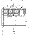
- FIG. 2 is an enlarged view showing an example of the top surface of the semiconductor device 100;
- FIG. FIG. 2B is a diagram showing the aa' cross section in FIG. 2A.
- FIG. 2B is a diagram showing a bb' cross section in FIG. 2A.
- FIG. 2B is a diagram showing a cc′ cross section in FIG. 2A.
- FIG. 2B is a diagram showing a dd' section in FIG. 2A.
- FIG. 2B is a diagram showing another example of the aa' cross section in FIG. 2A.
- FIG. 2B is a diagram showing another example of the aa' cross section in FIG. 2A.
- FIG. 2 is an enlarged view showing an example of the top surface of a semiconductor device 200 according to a comparative example
- FIG. 3B is a diagram showing the ee′ cross section in FIG. 3A.
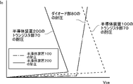
- 4 is a graph showing withstand voltage waveforms of the semiconductor device 100 and the semiconductor device 200;
- top one side in a direction parallel to the depth direction of the semiconductor substrate
- bottom One of the two main surfaces of a substrate, layer or other member
- front surface One of the two main surfaces of a substrate, layer or other member
- back surface One of the two main surfaces of a substrate, layer or other member.
- the directions of “up” and “down” are not limited to the direction of gravity or the direction when the semiconductor device is mounted.
- the Cartesian coordinate axes only specify the relative positions of the components and do not limit any particular orientation.
- the Z axis does not limit the height direction with respect to the ground.
- the +Z-axis direction and the ⁇ Z-axis direction are directions opposite to each other.
- the Z-axis direction is described without indicating positive or negative, it means the +Z-axis and the direction parallel to the Z-axis.
- orthogonal axes parallel to the front and back surfaces of the semiconductor substrate are defined as the X-axis and the Y-axis.
- the axis perpendicular to the front and back surfaces of the semiconductor substrate is defined as the Z-axis.
- the Z-axis direction may be referred to as the depth direction.
- the direction parallel to the front and back surfaces of the semiconductor substrate, including the X-axis and Y-axis, is sometimes referred to as the horizontal direction.
- the conductivity type of the doping region doped with impurities is described as P-type or N-type.
- an impurity may specifically refer to either an N-type donor or a P-type acceptor, and may be referred to as a dopant.
- doping means introducing donors or acceptors into a semiconductor substrate to make it a semiconductor exhibiting N-type conductivity or a semiconductor exhibiting P-type conductivity.
- doping concentration means the concentration of donors or the concentration of acceptors at thermal equilibrium.
- the net doping concentration means the net concentration including charge polarity, where the donor concentration is the positive ion concentration and the acceptor concentration is the negative ion concentration.
- the donor concentration is N D and the acceptor concentration is N A , then the net net doping concentration at any location is N D ⁇ N A.
- a donor has the function of supplying electrons to a semiconductor.
- the acceptor has the function of receiving electrons from the semiconductor.
- Donors and acceptors are not limited to impurities per se. For example, VOH defects in which vacancies (V), oxygen (O), and hydrogen (H) are combined in semiconductors function as donors that supply electrons.
- references herein to P-type or N-type refer to higher doping concentrations than P-type or N-type; references to P-type or N-type refer to higher doping than P-type or N-type. It means that the concentration is low.
- the term P++ type or N++ type in this specification means that the doping concentration is higher than that of the P+ type or N+ type.
- chemical concentration refers to the concentration of impurities measured regardless of the state of electrical activation. Chemical concentrations can be measured, for example, by secondary ion mass spectroscopy (SIMS).
- the net doping concentrations mentioned above can be measured by the voltage-capacitance method (CV method).
- the carrier concentration measured by the spreading resistance measurement method (SR method) may be used as the net doping concentration.
- the carrier concentration measured by the CV method or SR method may be a value in thermal equilibrium.
- the carrier concentration in the region may be used as the donor concentration.
- the carrier concentration in that region may be used as the acceptor concentration.
- the peak value may be the concentration of donors, acceptors, or net doping in the region.
- the average value of the concentration of donors, acceptors or net doping in the region may be used as the concentration of donors, acceptors or net doping.
- the carrier concentration measured by the SR method may be lower than the donor or acceptor concentration.
- the carrier mobility of the semiconductor substrate may be lower than the value in the crystalline state. A decrease in carrier mobility is caused by scattering of carriers due to disorder of the crystal structure due to lattice defects or the like.
- the donor or acceptor concentration calculated from the carrier concentration measured by the CV method or the SR method may be lower than the chemical concentration of the element representing the donor or acceptor.
- the donor concentration of phosphorus or arsenic as a donor or the acceptor concentration of boron (boron) as an acceptor in a silicon semiconductor is about 99% of these chemical concentrations.
- the donor concentration of hydrogen serving as a donor in a silicon semiconductor is about 0.1% to 10% of the chemical concentration of hydrogen.
- FIG. 1 is a diagram showing an example of the top surface of a semiconductor device 100 according to this embodiment.
- FIG. 1 shows the positions of each member projected onto the front surface of the semiconductor substrate 10 .
- FIG. 1 only some members of the semiconductor device 100 are shown, and some members are omitted.
- a semiconductor device 100 includes a semiconductor substrate 10 .
- the semiconductor substrate 10 has an edge 102 when viewed from above.
- simply referring to a top view means viewing from the front surface side of the semiconductor substrate 10 .
- the semiconductor substrate 10 of this example has two sets of edges 102 facing each other when viewed from above.
- the X-axis and Y-axis are parallel to one of the edges 102 .
- the Z-axis is perpendicular to the front surface of the semiconductor substrate 10 .
- An active portion 160 is provided on the semiconductor substrate 10 .
- the active portion 160 is a region through which a main current flows in the depth direction between the front surface and the back surface of the semiconductor substrate 10 when the semiconductor device 100 operates.
- An emitter electrode is provided above the active portion 160, but is omitted in FIG.
- At least one of a transistor section 70 including a transistor element such as an IGBT and a diode section 80 including a diode element such as a freewheeling diode (FWD) is provided in the active section 160 .
- the transistor portions 70 and the diode portions 80 are alternately arranged along a predetermined arrangement direction (X-axis direction in this example) on the front surface of the semiconductor substrate 10 .
- the region where the transistor section 70 is arranged is denoted by the symbol "I”
- the region where the diode section 80 is arranged is denoted by the symbol "F”.
- the direction perpendicular to the arrangement direction in top view may be referred to as the stretching direction (the Y-axis direction in FIG. 1).
- the transistor section 70 and the diode section 80 may each have a length in the extending direction. That is, the length in the Y-axis direction of the transistor section 70 is greater than the width in the X-axis direction. Similarly, the length in the Y-axis direction of the diode section 80 is greater than the width in the X-axis direction.
- the extending direction of the transistor portion 70 and the diode portion 80 may be the same as the longitudinal direction of each trench portion described later.
- the transistor section 70 has a P+ type collector region in a region in contact with the back surface of the semiconductor substrate 10 .
- the diode section 80 has an N+ type cathode region in a region in contact with the back surface of the semiconductor substrate 10 .
- the region provided with the collector region is referred to as a transistor section 70 . That is, the transistor portion 70 is a region that overlaps with the collector region when viewed from above.
- An N+ type cathode region may be provided on the back surface of the semiconductor substrate 10 in a region other than the collector region.
- a cathode region is provided on the lower surface of an extension region extending in the Y-axis direction from the transistor section 70 to a gate runner, which will be described later.
- the extension region is included in diode section 80 .
- a gate structure having an N-type emitter region, a P-type base region, a gate conductive portion and a gate insulating film is periodically arranged on the front surface side of the semiconductor substrate 10 .
- the semiconductor device 100 may have one or more pads above the semiconductor substrate 10 .
- the semiconductor device 100 shown in FIG. 1 has a gate pad G, but this is for illustration only.
- Semiconductor device 100 may have pads such as an anode pad, a cathode pad, and a current sensing pad. Each pad is arranged near the edge 102 . The vicinity of the edge 102 refers to a region between the edge 102 and the emitter electrode in top view. When the semiconductor device 100 is mounted, each pad may be connected to an external circuit via a wiring such as a wire.
- a gate potential is applied to the gate pad G.
- the gate pad G is electrically connected to the conductive portion of the gate trench portion of the active portion 160 .
- the semiconductor device 100 includes a gate runner 48 electrically connecting the gate pad G and the gate trench portion.
- the gate runner 48 is arranged between the active portion 160 and the edge 102 of the semiconductor substrate 10 when viewed from above.
- the gate runner 48 of this example surrounds the active portion 160 in top view.
- a region surrounded by the gate runners 48 in top view may be the active portion 160 .
- the gate runners 48 are arranged above the semiconductor substrate 10 .
- the gate runners 48 of this example may be formed of impurity-doped polysilicon or the like.
- the gate runner 48 is electrically connected to a gate conductive portion provided inside the gate trench portion via a gate insulating film.
- the semiconductor device 100 of this example includes a breakdown voltage structure portion 190 provided on the outer periphery of the active portion 160 .
- the breakdown voltage structure 190 of this example is arranged between the gate runner 48 and the edge 102 .
- the breakdown voltage structure 190 relaxes electric field concentration on the front surface side of the semiconductor substrate 10 .
- the pressure resistant structure 190 may have a guard ring 92 .
- Guard ring 92 is a P-type region in contact with the front surface of semiconductor substrate 10 .
- the withstand voltage structure 190 of this example has a plurality of guard rings 92, only one guard ring 92 is shown in FIG.
- the breakdown voltage structure 190 may further include at least one of a field plate and a resurf provided in an annular shape surrounding the active portion 160 .
- the semiconductor device 100 also includes a temperature sensing portion (not shown), which is a PN junction diode made of polysilicon or the like, and a current detecting portion (not shown) that operates in the same manner as the transistor portion provided in the active portion 160.
- a temperature sensing portion (not shown), which is a PN junction diode made of polysilicon or the like, and a current detecting portion (not shown) that operates in the same manner as the transistor portion provided in the active portion 160.
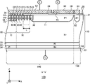
- FIG. 2A is an enlarged view showing an example of the top surface of the semiconductor device 100.
- FIG. FIG. 2A shows region A shown in FIG.
- the semiconductor device 100 includes a semiconductor substrate having a transistor section 70 including transistor elements such as IGBTs and a diode section 80 including diode elements such as a freewheeling diode (FWD).
- transistor elements such as IGBTs
- diode section 80 including diode elements such as a freewheeling diode (FWD).
- FWD freewheeling diode
- the transistor sections 70 and the diode sections 80 of this example are alternately arranged along the arrangement direction (the X-axis direction in this example).
- the diode section 80 is provided between the transistor section 70 adjacent to the withstand voltage structure section 190 and the withstand voltage structure section 190 when viewed from above. That is, the diode section 80 is arranged on the outermost side of the active section 160 .
- inside and outside means that the direction toward the center of the semiconductor device 100 is the inside, and the direction away from the center is the outside.
- a semiconductor device 100 of this example includes a gate trench portion 40, a dummy trench portion 30, a well region 11, an emitter region 12, a base region 14, and a contact region 15 provided on the front surface side of a semiconductor substrate.
- Each of the gate trench portion 40 and the dummy trench portion 30 is an example of the trench portion.
- the semiconductor device 100 of this example also includes a gate metal layer 50 and an emitter electrode 52 provided above the front surface of the semiconductor substrate. Gate metal layer 50 and emitter electrode 52 are provided separately from each other. Gate metal layer 50 and emitter electrode 52 are electrically insulated.
- An interlayer insulating film is provided between the emitter electrode 52 and the gate metal layer 50 and the front surface of the semiconductor substrate, but is omitted in FIG. 2A.
- Contact holes 49, 54 and 56 are provided through the interlayer insulating film of this example. In FIG. 2A, each contact hole is hatched with oblique lines.
- the emitter electrode 52 is provided above the gate trench portion 40 , the dummy trench portion 30 , the well region 11 , the emitter region 12 , the base region 14 and the contact region 15 .
- Emitter electrode 52 is electrically connected to emitter region 12 , base region 14 and contact region 15 on the front surface of the semiconductor substrate through contact hole 54 .
- the emitter electrode 52 is connected to the dummy conductive portion in the dummy trench portion 30 through a contact hole 56 .
- a connection portion 25 made of a conductive material such as impurity-doped polysilicon may be provided between the emitter electrode 52 and the dummy conductive portion.
- the connection portion 25 is provided on the front surface of the semiconductor substrate via an insulating film such as an interlayer insulating film and a dummy insulating film of the dummy trench portion 30 .
- the gate metal layer 50 is electrically connected with the gate runner 48 through the contact hole 49 .
- the gate runners 48 may be made of impurity-doped polysilicon or the like. Gate runners 48 connect to gate conductors within gate trenches 40 on the front surface of the semiconductor substrate. Gate runners 48 are not electrically connected to dummy conductive portions in dummy trench portion 30 and emitter electrode 52 .
- the gate runner 48 and the emitter electrode 52 are electrically separated by an insulator such as an interlayer insulating film and an oxide film.
- the gate runner 48 of this example is provided from below the contact hole 49 to the tip of the gate trench portion 40 .
- the gate conductive portion is exposed to the front surface of the semiconductor substrate at the tip portion of the gate trench portion 40 and is connected to the gate runner 48 .
- the emitter electrode 52 and the gate metal layer 50 are made of a conductive material containing metal.
- a conductive material containing metal For example, it is made of aluminum or an alloy containing aluminum as a main component (for example, an aluminum-silicon alloy).
- Each electrode may have a barrier metal made of titanium, a titanium compound, or the like under a region made of aluminum or the like.
- Each electrode may have a plug made of tungsten or the like in the contact hole.
- the plug may have a barrier metal on the side in contact with the semiconductor substrate, embed tungsten so as to be in contact with the barrier metal, and be formed of aluminum or the like on the tungsten.
- a plug is provided in a contact hole in contact with the contact region 15 or the base region 14 .
- a P++ type plug region is formed under the contact hole of the plug, and has a higher doping concentration than the contact region 15 . This can improve the contact resistance between the barrier metal and contact region 15 .
- the depth of the plug region is approximately 0.1 ⁇ m or less, and has a small region of 10% or less of the depth of the contact region 15 .
- the plug area has the following features.
- the latch-up resistance is improved by improving the contact resistance.
- the contact resistance between the barrier metal and the base region 14 is high, and conduction loss and switching loss increase. An increase in switching loss can be suppressed.
- the well region 11 overlaps the gate runner 48, extends the outer periphery of the active portion 160, and is provided in a ring shape when viewed from above.
- the well region 11 extends with a predetermined width even in a range that does not overlap with the gate runner 48, and is provided in an annular shape when viewed from above.
- the well region 11 of this example is provided away from the Y-axis direction end of the contact hole 54 on the gate runner 48 side.
- the well region 11 is a second conductivity type region having a higher doping concentration than the base region 14 .
- Gate runner 48 is electrically insulated from well region 11 .
- the base region 14 in this example is of P ⁇ type, and the well region 11 is of P+ type. Also, the well region 11 is formed from the front surface of the semiconductor substrate to a position deeper than the lower end of the base region 14 . Base region 14 is provided in contact with well region 11 in transistor section 70 and diode section 80 . Therefore, well region 11 is electrically connected to emitter electrode 52 .
- Each of the transistor section 70 and the diode section 80 has a plurality of trench sections arranged in the arrangement direction.
- One or more gate trench portions 40 are provided in the transistor portion 70 of this example along the arrangement direction.
- a plurality of dummy trench portions 30 are provided along the array direction in the diode portion 80 of this example.
- the gate trench portion 40 is not provided in the diode portion 80 of this example.
- the gate trench portion 40 of this example connects the two straight portions 39 extending along the extending direction perpendicular to the arrangement direction (the portion of the trench that is linear along the extending direction) and the two straight portions 39 . It may have a tip 41 .
- At least part of the tip portion 41 may be provided in a curved shape when viewed from above.
- the tip portion 41 functions as a gate electrode to the gate trench portion 40 .
- electric field concentration at the end portion can be alleviated as compared with the case where the tip portion 41 is completed with the straight portion 39 .
- the transistor section 70 may be alternately provided with one or more gate trench sections 40 and one or more dummy trench sections 30 along the arrangement direction.
- the dummy trench portions 30 are provided between the respective straight portions 39 of the gate trench portion 40 .
- One dummy trench portion 30 may be provided between the straight portions 39, or a plurality of dummy trench portions 30 may be provided.
- the dummy trench portions 30 may not be provided, and the gate trench portions 40 may be provided. With such a structure, the electron current from the emitter region 12 can be increased, thereby reducing the ON voltage.
- the dummy trench portion 30 may have a linear shape extending in the extending direction, and may have a linear portion 29 and a tip portion 31 like the gate trench portion 40 .
- the semiconductor device 100 shown in FIG. 2A only the dummy trench portions 30 having the tip portions 31 are arranged. A portion 30 may be included.
- the diffusion depth of the well region 11 may be deeper than the depths of the gate trench portion 40 and the dummy trench portion 30 .
- Y-axis direction ends of the gate trench portion 40 and the dummy trench portion 30 are provided in the well region 11 when viewed from above. That is, the bottom of each trench in the depth direction is covered with the well region 11 at the end of each trench in the Y-axis direction. Also, the trench portion provided at the end in the X-axis direction may be covered with the well region 11 . As a result, electric field concentration at the bottom of each trench can be relaxed.
- a mesa portion is provided between each trench portion in the arrangement direction.
- the mesa portion refers to a region sandwiched between trench portions inside the semiconductor substrate.
- the depth position of the mesa portion is from the front surface of the semiconductor substrate to the lower end of the trench portion.
- the mesa portion of this example is sandwiched between adjacent trench portions in the X-axis direction, and is provided extending in the extension direction (Y-axis direction) along the trenches on the front surface of the semiconductor substrate.
- the transistor section 70 is provided with a mesa section 60 and the diode section 80 is provided with a mesa section 61 .
- simply referring to the mesa portion refers to the mesa portion 60 and the mesa portion 61 respectively.
- a base region 14 is provided in each mesa portion.
- at least one of the first conductivity type emitter region 12 and the second conductivity type contact region 15 may be provided in a region sandwiched between the base regions 14 in top view.
- the emitter region 12 in this example is of N+ type and the contact region 15 is of P+ type.
- Emitter region 12 and contact region 15 may be provided between base region 14 and the front surface of the semiconductor substrate in the depth direction.
- the mesa portion of the transistor portion 70 has the emitter region 12 exposed on the front surface of the semiconductor substrate.
- the emitter region 12 is provided in contact with the gate trench portion 40 .
- a contact region 15 exposed on the front surface of the semiconductor substrate is provided in the mesa portion in contact with the gate trench portion 40 .
- Each of the contact region 15 and the emitter region 12 in the mesa portion is provided from one trench portion to the other trench portion in the X-axis direction.
- the contact regions 15 and the emitter regions 12 of the mesa are alternately arranged along the extending direction (Y-axis direction) of the trench.
- the contact regions 15 and the emitter regions 12 of the mesa portion may be provided in stripes along the extension direction (Y-axis direction) of the trench portion.
- an emitter region 12 is provided in a region in contact with the trench portion, and a contact region 15 is provided in a region sandwiched between the emitter regions 12 .
- the mesa portion of the diode portion 80 is not provided with the emitter region 12 .
- a base region 14 may be provided on the upper surface of the mesa portion of the diode portion 80 .
- the base region 14 may be arranged over the mesa portion of the diode portion 80 .
- a contact hole 54 is provided above each mesa portion.
- the contact hole 54 is arranged in a region sandwiched between the base regions 14 in its extending direction (Y-axis direction).
- the contact hole 54 of this example is provided above each region of the contact region 15 , the base region 14 and the emitter region 12 .
- the contact hole 54 may be arranged in the center in the arrangement direction (X-axis direction) of the mesa portions.
- an N+ type cathode region 82 is provided in a region adjacent to the back surface of the semiconductor substrate.
- a P+ type collector region 22 may be provided in a region where the cathode region 82 is not provided on the back surface of the semiconductor substrate.
- the boundary between cathode region 82 and collector region 22 is indicated by a dashed line.
- an N+ type cathode region 82 may be provided on the back side of the semiconductor substrate.
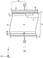
- FIG. 2B is a diagram showing the aa' cross section in FIG. 2A.
- the aa′ cross section is the XZ plane passing through the contact region 15 , the base region 14 , the gate trench portion 40 and the dummy trench portion 30 .
- a semiconductor device 100 of this example has a semiconductor substrate 10, an interlayer insulating film 38, an emitter electrode 52 and a collector electrode 24 in the aa' section.
- the interlayer insulating film 38 is provided on the front surface 21 of the semiconductor substrate 10 .
- the interlayer insulating film 38 is an insulating film such as silicate glass doped with an impurity such as boron or phosphorus. Interlayer insulating film 38 may be in contact with front surface 21 , and another film such as an oxide film may be provided between interlayer insulating film 38 and front surface 21 .
- the interlayer insulating film 38 is provided with the contact holes 54 described with reference to FIG. 2A.
- the emitter electrode 52 is provided on the front surface 21 of the semiconductor substrate 10 and the top surface of the interlayer insulating film 38 .
- Emitter electrode 52 is electrically connected to front surface 21 through contact hole 54 in interlayer insulating film 38 .
- a plug region 17 made of tungsten (W) or the like may be provided inside the contact hole 54 .
- Collector electrode 24 is provided on back surface 23 of semiconductor substrate 10 .
- Emitter electrode 52 and collector electrode 24 are made of a material containing metal or a laminated film thereof.
- the semiconductor substrate 10 may be a silicon substrate, a silicon carbide substrate, a nitride semiconductor substrate such as gallium nitride, or the like.
- the semiconductor substrate 10 of this example is a silicon substrate.
- the semiconductor substrate 10 has a first conductivity type drift region 18 .
- the drift region 18 in this example is of the N ⁇ type.
- Drift region 18 may be a remaining region of semiconductor substrate 10 that is not provided with other doping regions.
- one or more accumulation regions 16 may be provided above the drift region 18 in the Z-axis direction.
- the accumulation region 16 is a region in which the same dopant as the drift region 18 is accumulated at a higher concentration than the drift region 18 .
- the doping concentration of accumulation region 16 is higher than the doping concentration of drift region 18 .
- the accumulation region 16 in this example is of N type.
- the accumulation region 16 may be provided between the base region 14 and a trench bottom portion 75 described later in the transistor portion 70 .
- the accumulation region 16 may be provided only in the transistor section 70 or may be provided in both the transistor section 70 and the diode section 80 .
- an emitter region 12 is provided above the base region 14 and in contact with the front surface 21 .
- Emitter region 12 is provided in contact with gate trench portion 40 .
- the doping concentration of emitter region 12 is higher than the doping concentration of drift region 18 .
- the dopant for the emitter region 12 is, for example, arsenic (As), phosphorus (P), antimony (Sb), or the like.
- the diode section 80 is provided with the base region 14 exposed on the front surface 21 .
- Base region 14 of diode section 80 acts as an anode.
- a buffer region 20 of the first conductivity type may be provided below the drift region 18 .
- the buffer region 20 in this example is of N type.
- the doping concentration of buffer region 20 is higher than the doping concentration of drift region 18 .
- Buffer region 20 may function as a field stop layer that prevents a depletion layer extending from the lower surface side of base region 14 from reaching collector region 22 and cathode region 82 .
- a collector region 22 is provided below the buffer region 20 in the transistor section 70 .
- Collector region 22 may be provided in contact with cathode region 82 on rear surface 23 .
- a cathode region 82 is provided below the buffer region 20 in the diode section 80 .
- the cathode region 82 may be provided at the same depth as the collector region 22 of the transistor section 70 .
- the diode section 80 may function as a freewheeling diode (FWD) that allows a freewheeling current to flow in the opposite direction when the transistor section 70 is turned off.
- FWD freewheeling diode
- a gate trench portion 40 and a dummy trench portion 30 are provided in the semiconductor substrate 10 . Gate trench portion 40 and dummy trench portion 30 are provided to reach drift region 18 through base region 14 and accumulation region 16 from front surface 21 .
- the fact that the trench penetrates the doping region is not limited to the order of forming the doping region and then forming the trench.
- a structure in which a doping region is formed between the trench portions after the trench portions are formed is also included in the structure in which the trench portion penetrates the doping regions.
- the gate trench portion 40 has a gate trench provided in the front surface 21, a gate insulating film 42 and a gate conductive portion 44.
- a gate insulating film 42 is provided to cover the inner wall of the gate trench.
- the gate insulating layer 42 may be formed of an oxide layer or a nitride layer.
- the gate conductive portion 44 is provided so as to fill the gate insulating film 42 inside the gate trench.
- the top surface of the gate conductive portion 44 may be in the same XY plane as the front surface 21 .
- the gate insulating film 42 insulates the gate conductive portion 44 from the semiconductor substrate 10 .
- the gate conductive portion 44 is formed of impurity-doped polysilicon or the like.
- the gate conductive portion 44 may be provided longer than the base region 14 in the depth direction. Gate trench portion 40 is covered with interlayer insulating film 38 on front surface 21 . When a predetermined voltage is applied to the gate conductive portion 44, a channel is formed by an electron inversion layer in the surface layer of the interface of the base region 14 in contact with the gate trench.
- the dummy trench portion 30 may have the same structure as the gate trench portion 40 in the XZ cross section.
- the dummy trench portion 30 has dummy trenches provided in the front surface 21 , a dummy insulating film 32 and a dummy conductive portion 34 .
- a dummy insulating film 32 is provided to cover the inner wall of the dummy trench.
- the dummy insulating film 32 may be formed of an oxide film or a nitride film.
- the dummy conductive portion 34 is provided so as to fill the inner side of the dummy insulating film 32 inside the dummy trench.
- the top surface of the dummy conductive portion 34 may be on the same XY plane as the front surface 21 .
- the dummy insulating film 32 insulates the dummy conductive portion 34 from the semiconductor substrate 10 .
- the dummy conductive portion 34 may be made of the same material as the gate conductive portion 44 .
- the gate trench portion 40 and the dummy trench portion 30 of this example are covered with an interlayer insulating film 38 on the front surface 21 .
- the bottoms of the dummy trench portion 30 and the gate trench portion 40 may be curved (curved in cross section) convex downward.
- the transistor section 70 has a P-type trench bottom section 75 provided at the lower end of the trench section.
- the trench bottom portion 75 of this example is provided below the accumulation region 16 .
- the lower end of the trench bottom portion 75 may be positioned below the bottom portion of the gate trench portion 40 .
- the trench bottom portion 75 may cover the bottom portion of the gate trench portion 40 .
- the doping concentration of trench bottom portion 75 is greater than the doping concentration of drift region 18 and less than the doping concentration of base region 14 .
- the doping concentration of the trench bottom portion 75 is 1E12 cm ⁇ 3 or more and 1E13 cm ⁇ 3 or less.
- the end of the trench bottom portion 75 on the positive side in the X-axis direction coincides with the boundary between the cathode region 82 and the collector region 22, but extends further toward the diode portion 80 side. It may be recessed into the transistor portion 70 .
- the trench bottom portion 75 may be an electrically floating floating layer.
- a floating layer refers to a layer that is not electrically connected to any electrode such as the emitter electrode 52 .
- FIG. 2C is a diagram showing a bb' section in FIG. 2A.
- the bb' section is the XZ plane passing through the emitter region 12, the contact region 15, the base region 14, the gate trench portion 40 and the dummy trench portion 30 in the vicinity of the boundary between the active portion 160 and the breakdown voltage structure portion 190.
- the diode section 80 of this example is provided between the transistor section 70 adjacent to the withstand voltage structure section 190 and the withstand voltage structure section 190 when viewed from above. In other words, the diode section 80 is arranged closest to the breakdown voltage structure section 190 side of the active section 160 .
- the transistor section 70 of this example has the trench bottom section 75 .
- the trench bottom portion 75 is not provided in part of the transistor portion 70, and the trench bottom portion 75 is separated from the well region 11 electrically connected to the emitter electrode 52.
- the transistor portion 70 if the trench bottom portion 75 is not provided in a certain range from the end portion on the side of the withstanding voltage structure portion 190, the turn-on characteristics are degraded according to the amount of decrease in the trench bottom portion 75.
- the trench bottom section 75 can be provided in the entire transistor section 70, so that turn-on characteristics can be improved.
- the breakdown voltage of the transistor portion 70 is improved.
- the breakdown voltage of the semiconductor device 100 as a whole is improved, and the latch-up resistance is improved.
- the well region 11 is separated from the emitter electrode 52 .
- the well region 11 and the emitter electrode 52 can be insulated by providing the interlayer insulating film 38 between the well region 11 and the emitter electrode 52 .
- the interlayer insulating film 38 extends from the breakdown voltage structure 190 over part of the diode section 80 provided on the outermost side of the active section 160 when viewed from above.
- the distance L between the edge of the interlayer insulating film 38 and the edge of the well region 11 may be 10 ⁇ m or more and 30 ⁇ m or less.
- the transistor portion 70 has an N-type accumulation region 16 between the base region 14 and the trench bottom portion 75 .
- the accumulation region 16 may be provided only in the transistor section 70 and not provided in the diode section 80 .
- the accumulation region 16 may be provided in both the transistor section 70 and the diode section 80 .
- the effect of accelerating injection of carriers (IE effect) can be enhanced and the ON voltage can be reduced.
- An N-type cathode region 82 may be provided on the back surface 23 side of the semiconductor substrate 10 in the breakdown voltage structure 190 . That is, the cathode region 82 may be continuously provided on the back surface 23 side of the semiconductor substrate 10 from the diode portion 80 to the breakdown voltage structure portion 190 so as to surround the outer periphery of the active portion 160 .
- FIG. 2D is a diagram showing a cc' section in FIG. 2A.
- the cc' section is the YZ plane passing through the base region 14 and the contact region 15 provided in the diode section 80 in the vicinity of the Y-axis negative side end of the active section 160 .
- the diode section 80 is provided on the outermost side of the active section 160 .
- the contact region 15 is provided on the front surface 21 of the semiconductor substrate 10 .
- the base region 14 is exposed to the front surface 21 of the semiconductor substrate 10 outside the contact region 15 in the Y-axis direction. That is, when viewed from above, in the diode section 80, the contact region 15 is sandwiched between the base regions 14 in the Y-axis direction.
- a well region 11 is provided in the vicinity of the Y-axis negative side end of the active portion 160 .
- the diffusion depth of well region 11 is deeper than base region 14 .
- the well region 11 may extend in the Y-axis direction so as to partially cover the bottom of the base region 14 .
- FIG. 2E is a diagram showing a dd' cross section in FIG. 2A.
- the dd' section is the YZ plane passing through the emitter region 12, the base region 14 and the contact region 15 provided in the transistor section 70 in the vicinity of the Y-axis negative side end of the active section 160.
- FIG. The dd' cross section passes through an extension region extending the transistor portion 70 in the Y-axis direction.
- a cathode region is provided on the underside of the extension region. That is, when viewed from above, the transistor section 70 is sandwiched between the diode sections 80 in the Y-axis direction.
- the emitter region 12 and the contact region 15 are provided on the front surface 21 of the semiconductor substrate 10 .
- the base region 14 is exposed to the front surface 21 of the semiconductor substrate 10 outside the contact region 15 in the Y-axis direction.
- the emitter region 12 and the contact region 15 are sandwiched between the base regions 14 in the Y-axis direction.
- An accumulation region 16 and a trench bottom portion 75 are provided above the drift region 18 in the transistor portion 70 .
- the trench bottom portion 75 is provided below the accumulation region 16 .
- the trench bottom portion 75 may be provided in contact with the bottom surface of the accumulation region 16 .
- FIG. 2F is a diagram showing another example of the aa' cross section in FIG. 2A.
- the aa' cross section is the XZ plane passing through the contact region 15, the base region 14, the gate trench portion 40 and the dummy trench portion 30 as in FIG. 2B.
- a semiconductor device 100 of this example has a semiconductor substrate 10, an interlayer insulating film 38, an emitter electrode 52 and a collector electrode 24 in the aa' section.
- the lower end of the trench bottom portion 75 in this example is located below the bottom portion of the gate trench portion 40 and covers the bottom portion of the gate trench portion 40 .
- the trench bottom portion 75 may be an electrically floating floating layer.
- the end portion of the trench bottom portion 75 on the positive side in the X-axis direction coincides with the boundary between the cathode region 82 and the collector region 22, but extends toward the diode portion 80 side. It may be recessed into the transistor portion 70 . This example can obtain the same effect as in FIG. 2B.
- FIG. 2G is a diagram showing another example of the aa' cross section in FIG. 2A.
- the aa' cross section is the XZ plane passing through the contact region 15, the base region 14, the gate trench portion 40 and the dummy trench portion 30 as in FIG. 2B.
- a semiconductor device 100 of this example has a semiconductor substrate 10, an interlayer insulating film 38, an emitter electrode 52 and a collector electrode 24 in the aa' section.
- FIG. 1 is provided apart from the accumulation region 16, that is, the drift region 18 is interposed between the accumulation region 16 and the trench bottom portion 75.
- the trench bottom portion 75 may be thinner than the accumulation region 16 or the drift region 18 between the accumulation region 16 and the trench bottom portion 75 in the depth direction of the semiconductor substrate 10 .
- the end of the trench bottom portion 75 on the positive side in the X-axis direction coincides with the boundary between the cathode region 82 and the collector region 22, but extends further toward the diode portion 80 side. It may be recessed into the transistor portion 70 . This example can obtain the same effect as in FIG. 2B.
- FIG. 3A is an enlarged view showing an example of the top surface of a semiconductor device 200 according to a comparative example. Similar to FIG. 2A, FIG. 3A shows the region A shown in FIG. In the semiconductor device 200, members common to those in the semiconductor device 100 are denoted by the same reference numerals.
- the transistor section 70 of the semiconductor device 200 is provided between the diode section 80 adjacent to the withstand voltage structure section 190 and the withstand voltage structure section 190 in top view. That is, unlike FIG. 2A, the transistor section 70 is arranged on the outermost side of the active section 160 . A contact hole 54 is provided above the well region 11 . Therefore, well region 11 is electrically connected to emitter electrode 52 (not shown).
- FIG. 3B is a diagram showing the ee' section in FIG. 3A.
- the ee' section is the XZ plane passing through the emitter region 12, the contact region 15, the base region 14, the gate trench portion 40 and the dummy trench portion 30.
- FIG. 3B is a diagram showing the ee' section in FIG. 3A.
- the ee' section is the XZ plane passing through the emitter region 12, the contact region 15, the base region 14, the gate trench portion 40 and the dummy trench portion 30.
- the transistor section 70 is arranged on the outermost side of the active section 160 .
- a P-type collector region 22 is provided on the back surface 23 side of the semiconductor substrate 10 . That is, the collector region 22 is continuously provided on the back surface 23 side of the semiconductor substrate 10 from the transistor portion 70 to the breakdown voltage structure portion 190 .
- the transistor section 70 of the semiconductor device 200 has a trench bottom section 75 . However, if the trench bottom portion 75 is provided in the entire transistor portion 70 provided on the outermost side of the active portion 160 , the trench bottom portion 75 contacts the well region 11 . Since the well region 11 is electrically connected to the emitter electrode 52, the trench bottom portion 75 is fixed at the emitter potential and current cannot flow.
- the trench bottom section 75 is not provided on the side of the breakdown voltage structure section 190 . This separates the trench bottom portion 75 from the well region 11 electrically connected to the emitter electrode 52 . Therefore, since the semiconductor device 200 has a smaller trench bottom portion 75 than the semiconductor device 100, the turn-on characteristics are degraded according to the difference. Also, the withstand voltage of the semiconductor device 200 is lower than that of the semiconductor device 100, and the latch-up resistance is lowered.
- FIG. 4 is a graph showing breakdown voltage waveforms of the semiconductor device 100 and the semiconductor device 200.
- the breakdown voltage of a device is determined by the breakdown voltage of the trench bottom where current tends to concentrate. Since the IGBT has a negative resistance, as the current Ic increases, the voltage Vce decreases and the current concentrates in the same place, such as the bottom of the trench. On the other hand, the FWD does not concentrate the current in one place because the voltage increases as the current Ic increases.
- the breakdown voltage of the IGBT is lower than that of the FWD, the breakdown voltage of the RC-IGBT is determined by the breakdown voltage of the FWD. Due to the influence of the parasitic thyristor inherent in the IGBT, there is a risk of latch-up when avalanche occurs due to current concentration. On the other hand, since the FWD does not have a parasitic thyristor, there is no risk of latch-up even if avalanche occurs due to current concentration.
- the solid line indicates the breakdown voltage waveform of the transistor section 70 of the semiconductor device 200
- the dashed-dotted line indicates the breakdown voltage waveform of the diode section 80.
- the breakdown voltage of the transistor section 70 is lower than that of the diode section 80 , so the breakdown voltage of the semiconductor device 200 is determined by the breakdown voltage of the transistor section 70 .
- the transistor portion 70 of the semiconductor device 100 is entirely provided with the trench bottom portion 75, so that the breakdown voltage is higher than that of the transistor portion 70 of the semiconductor device 200 according to the difference. rises.
- a dashed line indicates a breakdown voltage waveform of the transistor section 70 of the semiconductor device 100 .
- the breakdown voltage waveform of the transistor portion 70 of the semiconductor device 100 is parallel shifted to the right by the amount of the breakdown voltage increase from the breakdown voltage waveform of the transistor portion 70 of the semiconductor device 200 .
- the withstand voltage of the diode portion 80 of the semiconductor device 100 is the same as that of the semiconductor device 200 .
- the breakdown voltage of the transistor section 70 is higher than that of the diode section 80 , so the breakdown voltage of the semiconductor device 100 is determined by the breakdown voltage of the diode section 80 .
- the breakdown voltage waveform of the semiconductor device 100 follows the one-dot chain line in FIG.
- the breakdown voltage waveform of the semiconductor device 200 follows the solid line in FIG. In this way, the breakdown voltage of the semiconductor device 100 is higher than that of the semiconductor device 200, and even if avalanche occurs in the diode section 80, there is no fear of latch-up, so the avalanche resistance is improved.
- connection part 29 Straight portion 30 Dummy trench portion 31 Tip portion 32 Dummy insulating film 34 Dummy conductive portion 38 Interlayer insulating film 39 Straight line Part 40 Gate trench portion 41 Tip portion 42 Gate insulating film 44 Gate conductive portion 48 Gate runner 49 Contact hole 50 Gate metal layer 52 Emitter electrode 54 Contact hole 56 Contact hole 60 Mesa portion 61 Mesa portion 70 Transistor portion 75 Trench bottom portion 80 Diode portion 82 Cathode region 92 Guard ring 100 Semiconductor device 102 Edge 160 Active portion 190 ⁇ Breakdown structure part, 200 ... semiconductor device
Abstract
L'invention concerne un dispositif à semi-conducteur comportant une partie active comprenant une partie de transistor et une partie de diode, et une partie de structure de tension de claquage disposée au niveau d'une périphérie externe de la partie active, dans laquelle : la partie transistor comprend une région de dérive d'un premier type de conduction, disposée dans un substrat semi-conducteur, une région de base d'un second type de conduction, disposée au-dessus de la région de dérive, une partie de tranchée s'étendant d'une surface avant du substrat semi-conducteur à la région de dérive, et une partie inférieure de tranchée du second type de conduction, disposée au niveau d'une extrémité inférieure de la partie de tranchée ; et la partie de diode est disposée entre la partie de transistor à proximité étroite de la partie de structure de tension de claquage et de la partie de structure de tension de claquage telle que vue dans une vue de dessus.
Priority Applications (4)
| Application Number | Priority Date | Filing Date | Title |
|---|---|---|---|
| CN202180072400.1A CN116420219A (zh) | 2021-05-11 | 2021-12-08 | 半导体装置 |
| JP2023520756A JPWO2022239284A1 (fr) | 2021-05-11 | 2021-12-08 | |
| DE112021004621.7T DE112021004621T5 (de) | 2021-05-11 | 2021-12-08 | Halbleitervorrichtung |
| US18/305,387 US20230268342A1 (en) | 2021-05-11 | 2023-04-24 | Semiconductor device |
Applications Claiming Priority (2)
| Application Number | Priority Date | Filing Date | Title |
|---|---|---|---|
| JP2021080620 | 2021-05-11 | ||
| JP2021-080620 | 2021-05-11 |
Related Child Applications (1)
| Application Number | Title | Priority Date | Filing Date |
|---|---|---|---|
| US18/305,387 Continuation US20230268342A1 (en) | 2021-05-11 | 2023-04-24 | Semiconductor device |
Publications (1)
| Publication Number | Publication Date |
|---|---|
| WO2022239284A1 true WO2022239284A1 (fr) | 2022-11-17 |
Family
ID=84028076
Family Applications (1)
| Application Number | Title | Priority Date | Filing Date |
|---|---|---|---|
| PCT/JP2021/045100 WO2022239284A1 (fr) | 2021-05-11 | 2021-12-08 | Dispositif à semi-conducteur |
Country Status (5)
| Country | Link |
|---|---|
| US (1) | US20230268342A1 (fr) |
| JP (1) | JPWO2022239284A1 (fr) |
| CN (1) | CN116420219A (fr) |
| DE (1) | DE112021004621T5 (fr) |
| WO (1) | WO2022239284A1 (fr) |
Cited By (1)
| Publication number | Priority date | Publication date | Assignee | Title |
|---|---|---|---|---|
| WO2023140254A1 (fr) * | 2022-01-20 | 2023-07-27 | 富士電機株式会社 | Dispositif à semi-conducteurs |
Citations (5)
| Publication number | Priority date | Publication date | Assignee | Title |
|---|---|---|---|---|
| JP2005142243A (ja) * | 2003-11-05 | 2005-06-02 | Toyota Motor Corp | 絶縁ゲート型半導体装置およびその製造方法 |
| JP2016162855A (ja) * | 2015-02-27 | 2016-09-05 | 株式会社日立製作所 | 半導体装置およびそれを用いた電力変換装置 |
| JP2019161126A (ja) * | 2018-03-15 | 2019-09-19 | 富士電機株式会社 | 半導体装置 |
| JP2020115596A (ja) * | 2016-08-12 | 2020-07-30 | 富士電機株式会社 | 半導体装置および半導体装置の製造方法 |
| JP2021028930A (ja) * | 2019-08-09 | 2021-02-25 | 富士電機株式会社 | 半導体装置 |
Family Cites Families (1)
| Publication number | Priority date | Publication date | Assignee | Title |
|---|---|---|---|---|
| DE102017124871B4 (de) | 2017-10-24 | 2021-06-17 | Infineon Technologies Ag | Leistungshalbleiter-Vorrichtung und Verfahren zum Herstellen einer Leistungshalbleiter-Vorrichtung |
-
2021
- 2021-12-08 WO PCT/JP2021/045100 patent/WO2022239284A1/fr unknown
- 2021-12-08 CN CN202180072400.1A patent/CN116420219A/zh active Pending
- 2021-12-08 JP JP2023520756A patent/JPWO2022239284A1/ja active Pending
- 2021-12-08 DE DE112021004621.7T patent/DE112021004621T5/de active Pending
-
2023
- 2023-04-24 US US18/305,387 patent/US20230268342A1/en active Pending
Patent Citations (5)
| Publication number | Priority date | Publication date | Assignee | Title |
|---|---|---|---|---|
| JP2005142243A (ja) * | 2003-11-05 | 2005-06-02 | Toyota Motor Corp | 絶縁ゲート型半導体装置およびその製造方法 |
| JP2016162855A (ja) * | 2015-02-27 | 2016-09-05 | 株式会社日立製作所 | 半導体装置およびそれを用いた電力変換装置 |
| JP2020115596A (ja) * | 2016-08-12 | 2020-07-30 | 富士電機株式会社 | 半導体装置および半導体装置の製造方法 |
| JP2019161126A (ja) * | 2018-03-15 | 2019-09-19 | 富士電機株式会社 | 半導体装置 |
| JP2021028930A (ja) * | 2019-08-09 | 2021-02-25 | 富士電機株式会社 | 半導体装置 |
Cited By (2)
| Publication number | Priority date | Publication date | Assignee | Title |
|---|---|---|---|---|
| WO2023140254A1 (fr) * | 2022-01-20 | 2023-07-27 | 富士電機株式会社 | Dispositif à semi-conducteurs |
| WO2023140253A1 (fr) * | 2022-01-20 | 2023-07-27 | 富士電機株式会社 | Dispositif à semi-conducteur |
Also Published As
| Publication number | Publication date |
|---|---|
| JPWO2022239284A1 (fr) | 2022-11-17 |
| DE112021004621T5 (de) | 2023-06-22 |
| CN116420219A (zh) | 2023-07-11 |
| US20230268342A1 (en) | 2023-08-24 |
Similar Documents
| Publication | Publication Date | Title |
|---|---|---|
| US11532738B2 (en) | Semiconductor device | |
| US20230261095A1 (en) | Semiconductor device | |
| JP7211516B2 (ja) | 半導体装置 | |
| US20230071170A1 (en) | Semiconductor device | |
| US20230268342A1 (en) | Semiconductor device | |
| US10886389B2 (en) | Semiconductor device | |
| CN111052394B (zh) | 半导体装置 | |
| JP7459976B2 (ja) | 半導体装置 | |
| US11257910B2 (en) | Semiconductor device including transistor portion and diode portion | |
| EP3817039A1 (fr) | Dispositif à semi-conducteur | |
| JP7231065B2 (ja) | 半導体装置 | |
| JP7231064B2 (ja) | 半導体装置 | |
| US20240072110A1 (en) | Semiconductor device and manufacturing method of semiconductor device | |
| WO2023140253A1 (fr) | Dispositif à semi-conducteur | |
| WO2023224059A1 (fr) | Dispositif à semi-conducteur | |
| US20240120412A1 (en) | Semiconductor device | |
| WO2023063411A1 (fr) | Dispositif à semi-conducteurs | |
| JP2022161688A (ja) | 半導体装置 | |
| JP2022179212A (ja) | 半導体装置 | |
| JP2024035557A (ja) | 半導体装置 | |
| JP2023128635A (ja) | 半導体装置 |
Legal Events
| Date | Code | Title | Description |
|---|---|---|---|
| 121 | Ep: the epo has been informed by wipo that ep was designated in this application |
Ref document number: 21942012 Country of ref document: EP Kind code of ref document: A1 |
|
| ENP | Entry into the national phase |
Ref document number: 2023520756 Country of ref document: JP Kind code of ref document: A |