WO2023224059A1 - Dispositif à semi-conducteur - Google Patents
Dispositif à semi-conducteur Download PDFInfo
- Publication number
- WO2023224059A1 WO2023224059A1 PCT/JP2023/018390 JP2023018390W WO2023224059A1 WO 2023224059 A1 WO2023224059 A1 WO 2023224059A1 JP 2023018390 W JP2023018390 W JP 2023018390W WO 2023224059 A1 WO2023224059 A1 WO 2023224059A1
- Authority
- WO
- WIPO (PCT)
- Prior art keywords
- region
- doping concentration
- contact
- collector
- semiconductor substrate
- Prior art date
Links
- 239000004065 semiconductor Substances 0.000 title claims abstract description 203
- 239000000758 substrate Substances 0.000 claims abstract description 112
- 238000002347 injection Methods 0.000 claims description 46
- 239000007924 injection Substances 0.000 claims description 46
- 239000000386 donor Substances 0.000 description 35
- 239000000370 acceptor Substances 0.000 description 27
- 238000010586 diagram Methods 0.000 description 24
- 238000000034 method Methods 0.000 description 21
- 239000011229 interlayer Substances 0.000 description 15
- 239000000969 carrier Substances 0.000 description 9
- 239000012535 impurity Substances 0.000 description 9
- 239000000126 substance Substances 0.000 description 9
- OAICVXFJPJFONN-UHFFFAOYSA-N Phosphorus Chemical compound [P] OAICVXFJPJFONN-UHFFFAOYSA-N 0.000 description 7
- 238000009826 distribution Methods 0.000 description 7
- 229910052698 phosphorus Inorganic materials 0.000 description 7
- 239000011574 phosphorus Substances 0.000 description 7
- 229910052782 aluminium Inorganic materials 0.000 description 6
- XAGFODPZIPBFFR-UHFFFAOYSA-N aluminium Chemical compound [Al] XAGFODPZIPBFFR-UHFFFAOYSA-N 0.000 description 6
- 229910052739 hydrogen Inorganic materials 0.000 description 6
- 239000001257 hydrogen Substances 0.000 description 6
- 239000010410 layer Substances 0.000 description 6
- 230000002093 peripheral effect Effects 0.000 description 6
- 229910021420 polycrystalline silicon Inorganic materials 0.000 description 6
- 229920005591 polysilicon Polymers 0.000 description 6
- 229910052751 metal Inorganic materials 0.000 description 5
- 239000002184 metal Substances 0.000 description 5
- 238000009825 accumulation Methods 0.000 description 4
- QVGXLLKOCUKJST-UHFFFAOYSA-N atomic oxygen Chemical compound [O] QVGXLLKOCUKJST-UHFFFAOYSA-N 0.000 description 4
- 239000002019 doping agent Substances 0.000 description 4
- 229910052760 oxygen Inorganic materials 0.000 description 4
- 239000001301 oxygen Substances 0.000 description 4
- 238000003860 storage Methods 0.000 description 4
- UFHFLCQGNIYNRP-UHFFFAOYSA-N Hydrogen Chemical compound [H][H] UFHFLCQGNIYNRP-UHFFFAOYSA-N 0.000 description 3
- XUIMIQQOPSSXEZ-UHFFFAOYSA-N Silicon Chemical compound [Si] XUIMIQQOPSSXEZ-UHFFFAOYSA-N 0.000 description 3
- 230000007547 defect Effects 0.000 description 3
- 230000005684 electric field Effects 0.000 description 3
- 150000002431 hydrogen Chemical class 0.000 description 3
- 238000004519 manufacturing process Methods 0.000 description 3
- 239000000463 material Substances 0.000 description 3
- 230000000149 penetrating effect Effects 0.000 description 3
- 230000008569 process Effects 0.000 description 3
- 229910052710 silicon Inorganic materials 0.000 description 3
- 239000010703 silicon Substances 0.000 description 3
- 238000003892 spreading Methods 0.000 description 3
- 230000007480 spreading Effects 0.000 description 3
- ZOXJGFHDIHLPTG-UHFFFAOYSA-N Boron Chemical compound [B] ZOXJGFHDIHLPTG-UHFFFAOYSA-N 0.000 description 2
- 238000000137 annealing Methods 0.000 description 2
- 229910052785 arsenic Inorganic materials 0.000 description 2
- RQNWIZPPADIBDY-UHFFFAOYSA-N arsenic atom Chemical compound [As] RQNWIZPPADIBDY-UHFFFAOYSA-N 0.000 description 2
- 125000004429 atom Chemical group 0.000 description 2
- 230000004888 barrier function Effects 0.000 description 2
- 229910052796 boron Inorganic materials 0.000 description 2
- 230000015556 catabolic process Effects 0.000 description 2
- 239000004020 conductor Substances 0.000 description 2
- 238000001514 detection method Methods 0.000 description 2
- 230000000694 effects Effects 0.000 description 2
- 230000001747 exhibiting effect Effects 0.000 description 2
- 239000000852 hydrogen donor Substances 0.000 description 2
- 150000002500 ions Chemical class 0.000 description 2
- 239000007769 metal material Substances 0.000 description 2
- 229910000789 Aluminium-silicon alloy Inorganic materials 0.000 description 1
- BUGBHKTXTAQXES-UHFFFAOYSA-N Selenium Chemical compound [Se] BUGBHKTXTAQXES-UHFFFAOYSA-N 0.000 description 1
- 229910000676 Si alloy Inorganic materials 0.000 description 1
- NINIDFKCEFEMDL-UHFFFAOYSA-N Sulfur Chemical compound [S] NINIDFKCEFEMDL-UHFFFAOYSA-N 0.000 description 1
- RTAQQCXQSZGOHL-UHFFFAOYSA-N Titanium Chemical compound [Ti] RTAQQCXQSZGOHL-UHFFFAOYSA-N 0.000 description 1
- KPSZQYZCNSCYGG-UHFFFAOYSA-N [B].[B] Chemical compound [B].[B] KPSZQYZCNSCYGG-UHFFFAOYSA-N 0.000 description 1
- 230000004913 activation Effects 0.000 description 1
- CSDREXVUYHZDNP-UHFFFAOYSA-N alumanylidynesilicon Chemical compound [Al].[Si] CSDREXVUYHZDNP-UHFFFAOYSA-N 0.000 description 1
- 229910052787 antimony Inorganic materials 0.000 description 1
- WATWJIUSRGPENY-UHFFFAOYSA-N antimony atom Chemical compound [Sb] WATWJIUSRGPENY-UHFFFAOYSA-N 0.000 description 1
- 239000012141 concentrate Substances 0.000 description 1
- 239000013078 crystal Substances 0.000 description 1
- 238000005520 cutting process Methods 0.000 description 1
- 238000009792 diffusion process Methods 0.000 description 1
- 230000012447 hatching Effects 0.000 description 1
- 238000009413 insulation Methods 0.000 description 1
- 238000005259 measurement Methods 0.000 description 1
- 238000000691 measurement method Methods 0.000 description 1
- 229910001092 metal group alloy Inorganic materials 0.000 description 1
- 238000012986 modification Methods 0.000 description 1
- 230000004048 modification Effects 0.000 description 1
- 238000005121 nitriding Methods 0.000 description 1
- 230000001590 oxidative effect Effects 0.000 description 1
- 238000001004 secondary ion mass spectrometry Methods 0.000 description 1
- 229910052711 selenium Inorganic materials 0.000 description 1
- 239000011669 selenium Substances 0.000 description 1
- 239000005368 silicate glass Substances 0.000 description 1
- 239000000243 solution Substances 0.000 description 1
- 230000000087 stabilizing effect Effects 0.000 description 1
- 229910052717 sulfur Inorganic materials 0.000 description 1
- 239000011593 sulfur Substances 0.000 description 1
- 239000002344 surface layer Substances 0.000 description 1
- 239000010936 titanium Substances 0.000 description 1
- 229910052719 titanium Inorganic materials 0.000 description 1
- 150000003609 titanium compounds Chemical class 0.000 description 1
- WFKWXMTUELFFGS-UHFFFAOYSA-N tungsten Chemical compound [W] WFKWXMTUELFFGS-UHFFFAOYSA-N 0.000 description 1
- 229910052721 tungsten Inorganic materials 0.000 description 1
- 239000010937 tungsten Substances 0.000 description 1
Images


Classifications
-
- H—ELECTRICITY
- H01—ELECTRIC ELEMENTS
- H01L—SEMICONDUCTOR DEVICES NOT COVERED BY CLASS H10
- H01L29/00—Semiconductor devices specially adapted for rectifying, amplifying, oscillating or switching and having potential barriers; Capacitors or resistors having potential barriers, e.g. a PN-junction depletion layer or carrier concentration layer; Details of semiconductor bodies or of electrodes thereof ; Multistep manufacturing processes therefor
- H01L29/02—Semiconductor bodies ; Multistep manufacturing processes therefor
- H01L29/06—Semiconductor bodies ; Multistep manufacturing processes therefor characterised by their shape; characterised by the shapes, relative sizes, or dispositions of the semiconductor regions ; characterised by the concentration or distribution of impurities within semiconductor regions
- H01L29/08—Semiconductor bodies ; Multistep manufacturing processes therefor characterised by their shape; characterised by the shapes, relative sizes, or dispositions of the semiconductor regions ; characterised by the concentration or distribution of impurities within semiconductor regions with semiconductor regions connected to an electrode carrying current to be rectified, amplified or switched and such electrode being part of a semiconductor device which comprises three or more electrodes
- H01L29/0821—Collector regions of bipolar transistors
-
- H—ELECTRICITY
- H01—ELECTRIC ELEMENTS
- H01L—SEMICONDUCTOR DEVICES NOT COVERED BY CLASS H10
- H01L29/00—Semiconductor devices specially adapted for rectifying, amplifying, oscillating or switching and having potential barriers; Capacitors or resistors having potential barriers, e.g. a PN-junction depletion layer or carrier concentration layer; Details of semiconductor bodies or of electrodes thereof ; Multistep manufacturing processes therefor
- H01L29/40—Electrodes ; Multistep manufacturing processes therefor
- H01L29/41—Electrodes ; Multistep manufacturing processes therefor characterised by their shape, relative sizes or dispositions
-
- H—ELECTRICITY
- H01—ELECTRIC ELEMENTS
- H01L—SEMICONDUCTOR DEVICES NOT COVERED BY CLASS H10
- H01L27/00—Devices consisting of a plurality of semiconductor or other solid-state components formed in or on a common substrate
- H01L27/02—Devices consisting of a plurality of semiconductor or other solid-state components formed in or on a common substrate including semiconductor components specially adapted for rectifying, oscillating, amplifying or switching and having potential barriers; including integrated passive circuit elements having potential barriers
- H01L27/04—Devices consisting of a plurality of semiconductor or other solid-state components formed in or on a common substrate including semiconductor components specially adapted for rectifying, oscillating, amplifying or switching and having potential barriers; including integrated passive circuit elements having potential barriers the substrate being a semiconductor body
- H01L27/06—Devices consisting of a plurality of semiconductor or other solid-state components formed in or on a common substrate including semiconductor components specially adapted for rectifying, oscillating, amplifying or switching and having potential barriers; including integrated passive circuit elements having potential barriers the substrate being a semiconductor body including a plurality of individual components in a non-repetitive configuration
- H01L27/0611—Devices consisting of a plurality of semiconductor or other solid-state components formed in or on a common substrate including semiconductor components specially adapted for rectifying, oscillating, amplifying or switching and having potential barriers; including integrated passive circuit elements having potential barriers the substrate being a semiconductor body including a plurality of individual components in a non-repetitive configuration integrated circuits having a two-dimensional layout of components without a common active region
- H01L27/0641—Devices consisting of a plurality of semiconductor or other solid-state components formed in or on a common substrate including semiconductor components specially adapted for rectifying, oscillating, amplifying or switching and having potential barriers; including integrated passive circuit elements having potential barriers the substrate being a semiconductor body including a plurality of individual components in a non-repetitive configuration integrated circuits having a two-dimensional layout of components without a common active region without components of the field effect type
- H01L27/0647—Bipolar transistors in combination with diodes, or capacitors, or resistors, e.g. vertical bipolar transistor and bipolar lateral transistor and resistor
- H01L27/0652—Vertical bipolar transistor in combination with diodes, or capacitors, or resistors
- H01L27/0664—Vertical bipolar transistor in combination with diodes
-
- H—ELECTRICITY
- H01—ELECTRIC ELEMENTS
- H01L—SEMICONDUCTOR DEVICES NOT COVERED BY CLASS H10
- H01L29/00—Semiconductor devices specially adapted for rectifying, amplifying, oscillating or switching and having potential barriers; Capacitors or resistors having potential barriers, e.g. a PN-junction depletion layer or carrier concentration layer; Details of semiconductor bodies or of electrodes thereof ; Multistep manufacturing processes therefor
- H01L29/02—Semiconductor bodies ; Multistep manufacturing processes therefor
- H01L29/06—Semiconductor bodies ; Multistep manufacturing processes therefor characterised by their shape; characterised by the shapes, relative sizes, or dispositions of the semiconductor regions ; characterised by the concentration or distribution of impurities within semiconductor regions
- H01L29/0603—Semiconductor bodies ; Multistep manufacturing processes therefor characterised by their shape; characterised by the shapes, relative sizes, or dispositions of the semiconductor regions ; characterised by the concentration or distribution of impurities within semiconductor regions characterised by particular constructional design considerations, e.g. for preventing surface leakage, for controlling electric field concentration or for internal isolations regions
- H01L29/0607—Semiconductor bodies ; Multistep manufacturing processes therefor characterised by their shape; characterised by the shapes, relative sizes, or dispositions of the semiconductor regions ; characterised by the concentration or distribution of impurities within semiconductor regions characterised by particular constructional design considerations, e.g. for preventing surface leakage, for controlling electric field concentration or for internal isolations regions for preventing surface leakage or controlling electric field concentration
- H01L29/0611—Semiconductor bodies ; Multistep manufacturing processes therefor characterised by their shape; characterised by the shapes, relative sizes, or dispositions of the semiconductor regions ; characterised by the concentration or distribution of impurities within semiconductor regions characterised by particular constructional design considerations, e.g. for preventing surface leakage, for controlling electric field concentration or for internal isolations regions for preventing surface leakage or controlling electric field concentration for increasing or controlling the breakdown voltage of reverse biased devices
- H01L29/0615—Semiconductor bodies ; Multistep manufacturing processes therefor characterised by their shape; characterised by the shapes, relative sizes, or dispositions of the semiconductor regions ; characterised by the concentration or distribution of impurities within semiconductor regions characterised by particular constructional design considerations, e.g. for preventing surface leakage, for controlling electric field concentration or for internal isolations regions for preventing surface leakage or controlling electric field concentration for increasing or controlling the breakdown voltage of reverse biased devices by the doping profile or the shape or the arrangement of the PN junction, or with supplementary regions, e.g. junction termination extension [JTE]
- H01L29/0619—Semiconductor bodies ; Multistep manufacturing processes therefor characterised by their shape; characterised by the shapes, relative sizes, or dispositions of the semiconductor regions ; characterised by the concentration or distribution of impurities within semiconductor regions characterised by particular constructional design considerations, e.g. for preventing surface leakage, for controlling electric field concentration or for internal isolations regions for preventing surface leakage or controlling electric field concentration for increasing or controlling the breakdown voltage of reverse biased devices by the doping profile or the shape or the arrangement of the PN junction, or with supplementary regions, e.g. junction termination extension [JTE] with a supplementary region doped oppositely to or in rectifying contact with the semiconductor containing or contacting region, e.g. guard rings with PN or Schottky junction
- H01L29/0623—Buried supplementary region, e.g. buried guard ring
-
- H—ELECTRICITY
- H01—ELECTRIC ELEMENTS
- H01L—SEMICONDUCTOR DEVICES NOT COVERED BY CLASS H10
- H01L29/00—Semiconductor devices specially adapted for rectifying, amplifying, oscillating or switching and having potential barriers; Capacitors or resistors having potential barriers, e.g. a PN-junction depletion layer or carrier concentration layer; Details of semiconductor bodies or of electrodes thereof ; Multistep manufacturing processes therefor
- H01L29/66—Types of semiconductor device ; Multistep manufacturing processes therefor
- H01L29/66007—Multistep manufacturing processes
- H01L29/66075—Multistep manufacturing processes of devices having semiconductor bodies comprising group 14 or group 13/15 materials
- H01L29/66227—Multistep manufacturing processes of devices having semiconductor bodies comprising group 14 or group 13/15 materials the devices being controllable only by the electric current supplied or the electric potential applied, to an electrode which does not carry the current to be rectified, amplified or switched, e.g. three-terminal devices
- H01L29/66234—Bipolar junction transistors [BJT]
- H01L29/66325—Bipolar junction transistors [BJT] controlled by field-effect, e.g. insulated gate bipolar transistors [IGBT]
- H01L29/66333—Vertical insulated gate bipolar transistors
- H01L29/66348—Vertical insulated gate bipolar transistors with a recessed gate
-
- H—ELECTRICITY
- H01—ELECTRIC ELEMENTS
- H01L—SEMICONDUCTOR DEVICES NOT COVERED BY CLASS H10
- H01L29/00—Semiconductor devices specially adapted for rectifying, amplifying, oscillating or switching and having potential barriers; Capacitors or resistors having potential barriers, e.g. a PN-junction depletion layer or carrier concentration layer; Details of semiconductor bodies or of electrodes thereof ; Multistep manufacturing processes therefor
- H01L29/66—Types of semiconductor device ; Multistep manufacturing processes therefor
- H01L29/68—Types of semiconductor device ; Multistep manufacturing processes therefor controllable by only the electric current supplied, or only the electric potential applied, to an electrode which does not carry the current to be rectified, amplified or switched
- H01L29/70—Bipolar devices
- H01L29/72—Transistor-type devices, i.e. able to continuously respond to applied control signals
- H01L29/739—Transistor-type devices, i.e. able to continuously respond to applied control signals controlled by field-effect, e.g. bipolar static induction transistors [BSIT]
- H01L29/7393—Insulated gate bipolar mode transistors, i.e. IGBT; IGT; COMFET
- H01L29/7395—Vertical transistors, e.g. vertical IGBT
- H01L29/7396—Vertical transistors, e.g. vertical IGBT with a non planar surface, e.g. with a non planar gate or with a trench or recess or pillar in the surface of the emitter, base or collector region for improving current density or short circuiting the emitter and base regions
- H01L29/7397—Vertical transistors, e.g. vertical IGBT with a non planar surface, e.g. with a non planar gate or with a trench or recess or pillar in the surface of the emitter, base or collector region for improving current density or short circuiting the emitter and base regions and a gate structure lying on a slanted or vertical surface or formed in a groove, e.g. trench gate IGBT
-
- H—ELECTRICITY
- H01—ELECTRIC ELEMENTS
- H01L—SEMICONDUCTOR DEVICES NOT COVERED BY CLASS H10
- H01L29/00—Semiconductor devices specially adapted for rectifying, amplifying, oscillating or switching and having potential barriers; Capacitors or resistors having potential barriers, e.g. a PN-junction depletion layer or carrier concentration layer; Details of semiconductor bodies or of electrodes thereof ; Multistep manufacturing processes therefor
- H01L29/66—Types of semiconductor device ; Multistep manufacturing processes therefor
- H01L29/68—Types of semiconductor device ; Multistep manufacturing processes therefor controllable by only the electric current supplied, or only the electric potential applied, to an electrode which does not carry the current to be rectified, amplified or switched
- H01L29/76—Unipolar devices, e.g. field effect transistors
- H01L29/772—Field effect transistors
- H01L29/78—Field effect transistors with field effect produced by an insulated gate
-
- H—ELECTRICITY
- H01—ELECTRIC ELEMENTS
- H01L—SEMICONDUCTOR DEVICES NOT COVERED BY CLASS H10
- H01L29/00—Semiconductor devices specially adapted for rectifying, amplifying, oscillating or switching and having potential barriers; Capacitors or resistors having potential barriers, e.g. a PN-junction depletion layer or carrier concentration layer; Details of semiconductor bodies or of electrodes thereof ; Multistep manufacturing processes therefor
- H01L29/66—Types of semiconductor device ; Multistep manufacturing processes therefor
- H01L29/86—Types of semiconductor device ; Multistep manufacturing processes therefor controllable only by variation of the electric current supplied, or only the electric potential applied, to one or more of the electrodes carrying the current to be rectified, amplified, oscillated or switched
- H01L29/861—Diodes
- H01L29/8613—Mesa PN junction diodes
-
- H—ELECTRICITY
- H01—ELECTRIC ELEMENTS
- H01L—SEMICONDUCTOR DEVICES NOT COVERED BY CLASS H10
- H01L29/00—Semiconductor devices specially adapted for rectifying, amplifying, oscillating or switching and having potential barriers; Capacitors or resistors having potential barriers, e.g. a PN-junction depletion layer or carrier concentration layer; Details of semiconductor bodies or of electrodes thereof ; Multistep manufacturing processes therefor
- H01L29/66—Types of semiconductor device ; Multistep manufacturing processes therefor
- H01L29/86—Types of semiconductor device ; Multistep manufacturing processes therefor controllable only by variation of the electric current supplied, or only the electric potential applied, to one or more of the electrodes carrying the current to be rectified, amplified, oscillated or switched
- H01L29/861—Diodes
- H01L29/868—PIN diodes
-
- H—ELECTRICITY
- H01—ELECTRIC ELEMENTS
- H01L—SEMICONDUCTOR DEVICES NOT COVERED BY CLASS H10
- H01L27/00—Devices consisting of a plurality of semiconductor or other solid-state components formed in or on a common substrate
- H01L27/02—Devices consisting of a plurality of semiconductor or other solid-state components formed in or on a common substrate including semiconductor components specially adapted for rectifying, oscillating, amplifying or switching and having potential barriers; including integrated passive circuit elements having potential barriers
- H01L27/04—Devices consisting of a plurality of semiconductor or other solid-state components formed in or on a common substrate including semiconductor components specially adapted for rectifying, oscillating, amplifying or switching and having potential barriers; including integrated passive circuit elements having potential barriers the substrate being a semiconductor body
- H01L27/06—Devices consisting of a plurality of semiconductor or other solid-state components formed in or on a common substrate including semiconductor components specially adapted for rectifying, oscillating, amplifying or switching and having potential barriers; including integrated passive circuit elements having potential barriers the substrate being a semiconductor body including a plurality of individual components in a non-repetitive configuration
- H01L27/07—Devices consisting of a plurality of semiconductor or other solid-state components formed in or on a common substrate including semiconductor components specially adapted for rectifying, oscillating, amplifying or switching and having potential barriers; including integrated passive circuit elements having potential barriers the substrate being a semiconductor body including a plurality of individual components in a non-repetitive configuration the components having an active region in common
- H01L27/0705—Devices consisting of a plurality of semiconductor or other solid-state components formed in or on a common substrate including semiconductor components specially adapted for rectifying, oscillating, amplifying or switching and having potential barriers; including integrated passive circuit elements having potential barriers the substrate being a semiconductor body including a plurality of individual components in a non-repetitive configuration the components having an active region in common comprising components of the field effect type
- H01L27/0727—Devices consisting of a plurality of semiconductor or other solid-state components formed in or on a common substrate including semiconductor components specially adapted for rectifying, oscillating, amplifying or switching and having potential barriers; including integrated passive circuit elements having potential barriers the substrate being a semiconductor body including a plurality of individual components in a non-repetitive configuration the components having an active region in common comprising components of the field effect type in combination with diodes, or capacitors or resistors
Definitions
- the present invention relates to a semiconductor device.
- Patent Documents 1 and 2 Description of the Related Art Conventionally, semiconductor devices including IGBTs and the like have been known (for example, see Patent Documents 1 and 2). [Prior art documents] [Patent document] [Patent Document 1] JP 2015-023118 A [Patent Document 2] JP 2018-049866 A
- a first aspect of the present invention provides a semiconductor device.
- the semiconductor device may include a semiconductor substrate that has an upper surface and a lower surface and is provided with a drift region of a first conductivity type.
- the semiconductor device may include an emitter region of a first conductivity type that is provided in contact with the upper surface of the semiconductor substrate and has a higher doping concentration than the drift region.
- Any of the semiconductor devices described above may include a base region of a second conductivity type provided in contact with the emitter region.
- Any of the above semiconductor devices may include a second conductivity type collector region provided between the drift region and the lower surface of the semiconductor substrate.
- any of the semiconductor devices described above may include a floating region of a first conductivity type that is provided in contact with an upper surface of the collector region and has a higher doping concentration than the collector region.
- the collector region may have a first region not covered by the floating region and a second region covered by the floating region.
- the doping concentration of the floating region may be 10 times or more the doping concentration of the collector region.
- the thickness of the floating region in the depth direction may be 0.5 times or more the thickness of the collector region in the depth direction.
- the product of the doping concentration and the thickness in the depth direction of the floating region may be 10 times or more the product of the doping concentration and the thickness in the depth direction of the collector region.
- the area of the first region in the unit area of the collector region in top view is S 1
- the area of the second region is S 2
- the injection efficiency of the first region is ⁇ 1.
- any of the above semiconductor devices may include a buffer region formed between the collector region and the drift region and having a higher doping concentration than the drift region.
- the floating region may be arranged between the buffer region and the collector region.
- the doping concentration of the floating region may be higher than the doping concentration of the buffer region.
- the area of the first region in a unit area of the collector region in a top view may be S 1 and the area of the second region may be S 2 .
- the average doping concentration D C of the collector region may be given by the following formula using the doping concentration N A of the collector region in the first region.
- D C S 1 ⁇ N A /(S 1 +S 2 )
- the doping concentration N A of the collector region in the first region may be higher than the average doping concentration D C .
- the ratio ⁇ of the area S2 of the second region to the area S1 of the first region may be given by the following formula.
- a plurality of gate trench portions may be provided from the upper surface of the semiconductor substrate to the drift region and in contact with the emitter region and the base region, and arranged along the arrangement direction.
- the first region and the second region may be arranged alternately along the arrangement direction.
- any of the above semiconductor devices may include an active region including the emitter region and the base region.
- Any of the semiconductor devices described above may include a well region of a second conductivity type that surrounds the active region in a top view and is provided in contact with the upper surface of the semiconductor substrate.
- Any of the semiconductor devices described above may include an edge termination structure disposed between the well region and an edge of the semiconductor substrate.
- both the first region and the second region may be provided in the active region.
- the edge termination structure portion may be provided with the second region and may not be provided with the first region.
- the second region may be provided at a position overlapping with the well region, and the first region may not be provided.
- the second region of the edge termination structure may be provided to extend to a position overlapping with the emitter region of the active region.
- any of the above semiconductor devices may include a gate trench portion provided from the upper surface of the semiconductor substrate to the drift region and in contact with the emitter region and the base region.
- the first region may be provided at a position overlapping with the gate trench portion.
- any of the above semiconductor devices may include a contact region that is provided in contact with the upper surface of the semiconductor substrate and has a higher doping concentration than the base region.
- the contact area ratio of the first region may be higher than the contact area ratio of the second region.
- the contact area ratio may be a ratio of an area of the contact region exposed on the upper surface of the semiconductor substrate to a unit area.
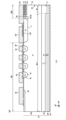
- FIG. 1 is a top view showing an example of a semiconductor device 100 according to one embodiment of the present invention.
- 2 is an enlarged view of region D in FIG. 1.
- FIG. 3 is a diagram showing an example of a cross section taken along line ee in FIG. 2.
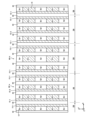
- FIG. It is a figure showing an example of arrangement of the 1st field 26 and the 2nd field 28 in top view.
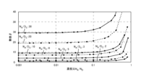
- 7 is a diagram showing characteristics for determining the area S2 of the second region 28 with respect to the area S1 of the first region 26.
- FIG. It is a figure showing an example of arrangement of the 1st field 26 and the 2nd field 28 in top view.
- FIG. 2 is a diagram showing an example of a cross section taken along the line aa in FIG. 1; FIG.
- FIG. 7 is a diagram showing another example of the aa cross section.
- 3 is a diagram illustrating an example of the arrangement of emitter regions 12 and contact regions 15 when viewed from above.
- FIG. FIG. 7 is a diagram showing another example of the aa cross section.
- 3 is a diagram illustrating an example of the arrangement of emitter regions 12 and contact regions 15 when viewed from above.
- FIG. FIG. 2 is a diagram showing an example of a cross section taken along line bb in FIG. 1;
- FIG. 2 is a diagram showing an example of a cross section taken along line bb in FIG. 1;
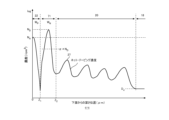
- 4 is a diagram showing an example of a net doping concentration distribution along line cc in FIG. 3.
- FIG. 3 is a diagram showing the relationship between the set value of the dose of P-type impurity implanted into the collector region 22 and the variation in the doping concentration of the collector region 22.
- FIG. 3 is a diagram showing the relationship between the set value of the dose of P-type
- one side in the direction parallel to the depth direction of the semiconductor substrate is referred to as "upper”, and the other side is referred to as “lower”.
- one surface is referred to as the upper surface and the other surface is referred to as the lower surface.
- the “up” and “down” directions are not limited to the gravitational direction or the direction in which the semiconductor device is mounted.
- orthogonal coordinate axes of the X-axis, Y-axis, and Z-axis only specify the relative positions of the components and do not limit specific directions.
- the Z axis does not limit the height direction relative to the ground.
- the +Z-axis direction and the -Z-axis direction are directions opposite to each other.
- the Z-axis direction is described without indicating positive or negative, it means a direction parallel to the +Z-axis and the -Z-axis.
- orthogonal axes parallel to the top and bottom surfaces of the semiconductor substrate are referred to as the X axis and the Y axis. Further, the axis perpendicular to the upper and lower surfaces of the semiconductor substrate is defined as the Z axis.
- the direction of the Z-axis may be referred to as the depth direction.
- a direction parallel to the top and bottom surfaces of the semiconductor substrate, including the X-axis and Y-axis may be referred to as a horizontal direction.
- the region from the center of the semiconductor substrate in the depth direction to the top surface of the semiconductor substrate is sometimes referred to as the top surface side.
- the region from the center of the semiconductor substrate in the depth direction to the lower surface of the semiconductor substrate may be referred to as the lower surface side.
- the conductivity type of the doped region doped with impurities is described as P type or N type.
- an impurity may particularly mean either an N-type donor or a P-type acceptor, and may be referred to as a dopant.
- doping means introducing a donor or an acceptor into a semiconductor substrate to make it a semiconductor exhibiting an N-type conductivity type or a semiconductor exhibiting a P-type conductivity type.
- doping concentration refers to the donor concentration or acceptor concentration at thermal equilibrium.
- the net doping concentration means the net concentration obtained by adding together the donor concentration, which is the positive ion concentration, and the acceptor concentration, which is the negative ion concentration, including charge polarity.
- the donor concentration is N D and the acceptor concentration is N A
- the net net doping concentration at any location is N D ⁇ NA .
- the net doping concentration may be simply referred to as doping concentration.
- the donor has the function of supplying electrons to the semiconductor.
- the acceptor has the function of receiving electrons from the semiconductor.
- Donors and acceptors are not limited to impurities themselves.
- a VOH defect in which vacancies (V), oxygen (O), and hydrogen (H) are bonded together in a semiconductor functions as a donor that supplies electrons.
- VOH defects may be referred to as hydrogen donors.
- the semiconductor substrate herein has N-type bulk donors distributed throughout.
- the bulk donor is a donor made from a dopant that is substantially uniformly contained in the ingot during manufacture of the ingot that is the source of the semiconductor substrate.
- the bulk donor in this example is an element other than hydrogen.
- Bulk donor dopants include, but are not limited to, phosphorus, antimony, arsenic, selenium or sulfur.
- the bulk donor in this example is phosphorus.
- Bulk donors are also included in the P-type region.
- the semiconductor substrate may be a wafer cut from a semiconductor ingot, or may be a chip obtained by cutting the wafer into pieces.
- a semiconductor ingot may be manufactured by any one of the Czochralski method (CZ method), the magnetic field Czochralski method (MCZ method), and the float zone method (FZ method).
- the ingot in this example is manufactured by the MCZ method.
- the oxygen concentration contained in the substrate manufactured by the MCZ method is 1 ⁇ 10 17 to 7 ⁇ 10 17 /cm 3 .
- the oxygen concentration contained in the substrate manufactured by the FZ method is 1 ⁇ 10 15 to 5 ⁇ 10 16 /cm 3 .
- Hydrogen donors tend to be generated more easily when the oxygen concentration is high.
- the bulk donor concentration may be a chemical concentration of bulk donors distributed throughout the semiconductor substrate, and may be between 90% and 100% of the chemical concentration.
- the semiconductor substrate may be a non-doped substrate that does not contain a dopant such as phosphorus.
- the bulk donor concentration (D0) of the non-doped substrate is, for example, 1 ⁇ 10 10 /cm 3 or more and 5 ⁇ 10 12 /cm 3 or less.
- the bulk donor concentration (D0) of the non-doped substrate is preferably 1 ⁇ 10 11 /cm 3 or more.
- the bulk donor concentration (D0) of the non-doped substrate is preferably 5 ⁇ 10 12 /cm 3 or less.
- each concentration in the present invention may be a value at room temperature. As an example of the value at room temperature, the value at 300K (Kelvin) (about 26.9°C) may be used.
- the doping concentration when described as P+ type or N+ type, it means that the doping concentration is higher than P type or N type, and when described as P ⁇ type or N ⁇ type, it means that the doping concentration is higher than P type or N type. It means that the concentration is low. Further, in this specification, when it is described as P++ type or N++ type, it means that the doping concentration is higher than that of P+ type or N+ type.
- the unit system in this specification is the SI unit system unless otherwise specified. Although the unit of length is sometimes expressed in cm, various calculations may be performed after converting to meters (m).
- chemical concentration refers to the atomic density of impurities measured regardless of the state of electrical activation.
- the chemical concentration can be measured, for example, by secondary ion mass spectrometry (SIMS).
- the above-mentioned net doping concentration can be measured by voltage-capacitance measurement (CV method).
- the carrier concentration measured by the spreading resistance measurement method (SR method) may be taken as the net doping concentration.
- the carrier concentration measured by the CV method or the SR method may be a value in a thermal equilibrium state.
- the donor concentration is sufficiently higher than the acceptor concentration, so the carrier concentration in this region may be taken as the donor concentration.
- the carrier concentration in the region may be set as the acceptor concentration.
- the doping concentration of the N-type region may be referred to as a donor concentration
- the doping concentration of the P-type region may be referred to as an acceptor concentration.
- the peak value may be taken as the donor, acceptor, or net doping concentration in the region.
- the average value of the donor, acceptor, or net doping concentration in the region may be taken as the donor, acceptor, or net doping concentration.
- atoms/cm 3 or /cm 3 is used to express the concentration per unit volume. This unit is used for donor or acceptor concentration or chemical concentration within a semiconductor substrate. The atoms notation may be omitted.
- the carrier concentration measured by the SR method may be lower than the donor or acceptor concentration.
- the carrier mobility of the semiconductor substrate may be lower than the value in the crystalline state. The decrease in carrier mobility occurs when carriers are scattered due to disorder of the crystal structure due to lattice defects or the like.
- the concentration of the donor or acceptor calculated from the carrier concentration measured by the CV method or the SR method may be lower than the chemical concentration of the element representing the donor or acceptor.
- the donor concentration of phosphorus or arsenic as a donor, or the acceptor concentration of boron (boron) as an acceptor is about 99% of these chemical concentrations.
- the donor concentration of hydrogen, which serves as a donor in a silicon semiconductor is about 0.1% to 10% of the chemical concentration of hydrogen.
- FIG. 1 is a top view showing an example of a semiconductor device 100 according to one embodiment of the present invention.
- FIG. 1 the positions of each member projected onto the upper surface of the semiconductor substrate 10 are shown.
- FIG. 1 only some members of the semiconductor device 100 are shown, and some members are omitted.
- the semiconductor device 100 includes a semiconductor substrate 10.
- the semiconductor substrate 10 is a substrate made of a semiconductor material.
- the semiconductor substrate 10 is a silicon substrate.
- the semiconductor substrate 10 has an edge 162 when viewed from above. In this specification, when simply referred to as a top view, it means viewed from the top surface side of the semiconductor substrate 10.
- the semiconductor substrate 10 of this example has two sets of end sides 162 that face each other when viewed from above. In FIG. 1, the X and Y axes are parallel to either edge 162. Further, the Z axis is perpendicular to the top surface of the semiconductor substrate 10.
- An active part 160 is provided on the semiconductor substrate 10.
- the active portion 160 is a region where a main current flows in the depth direction between the upper surface and the lower surface of the semiconductor substrate 10 when the semiconductor device 100 operates.
- An emitter electrode is provided above the active region 160, but is omitted in FIG.
- the active portion 160 may refer to a region that overlaps with the emitter electrode when viewed from above. Furthermore, the region sandwiched between the active portions 160 in a top view may also be included in the active portions 160.
- the active section 160 is provided with a transistor section 70 including a transistor element such as an IGBT (Insulated Gate Bipolar Transistor).
- the active section 160 may further include a diode section 80 including a diode element such as a free-wheeling diode (FWD).
- FWD free-wheeling diode
- the transistor sections 70 and the diode sections 80 are alternately arranged along a predetermined arrangement direction (in this example, the X-axis direction) on the upper surface of the semiconductor substrate 10.
- the semiconductor device 100 of this example is a reverse conduction type IGBT (RC-IGBT).
- the region where the transistor section 70 is arranged is marked with the symbol "I"
- the region where the diode section 80 is arranged is marked with the symbol "F”.
- a direction perpendicular to the arrangement direction in a top view may be referred to as a stretching direction (Y-axis direction in FIG. 1).
- the transistor section 70 and the diode section 80 may each have a length in the extending direction. In other words, the length of the transistor section 70 in the Y-axis direction is greater than the width in the X-axis direction. Similarly, the length of the diode section 80 in the Y-axis direction is greater than the width in the X-axis direction.
- the extending direction of the transistor section 70 and the diode section 80 may be the same as the longitudinal direction of each trench section, which will be described later.
- the diode section 80 has an N+ type cathode region in a region in contact with the lower surface of the semiconductor substrate 10.
- the region provided with the cathode region is referred to as a diode section 80.
- the diode section 80 is a region that overlaps with the cathode region when viewed from above.
- a P+ type collector region may be provided on the lower surface of the semiconductor substrate 10 in a region other than the cathode region.
- the diode section 80 may also include an extension region 81 in which the diode section 80 is extended in the Y-axis direction to a gate wiring to be described later.
- a collector region is provided on the lower surface of the extension region 81.
- the transistor section 70 has a P+ type collector region in a region in contact with the lower surface of the semiconductor substrate 10. Further, in the transistor section 70, a gate structure including an N-type emitter region, a P-type base region, a gate conductive portion, and a gate insulating film is periodically arranged on the upper surface side of the semiconductor substrate 10.
- the semiconductor device 100 may have one or more pads above the semiconductor substrate 10.
- the semiconductor device 100 of this example has a gate pad 164.
- the semiconductor device 100 may have pads such as an anode pad, a cathode pad, and a current detection pad. Each pad is located near the edge 162.
- the vicinity of the edge 162 refers to the area between the edge 162 and the emitter electrode in a top view.
- each pad may be connected to an external circuit via wiring such as a wire.
- a gate potential is applied to the gate pad 164.
- the gate pad 164 is electrically connected to a conductive portion of the gate trench portion of the active portion 160 .
- the semiconductor device 100 includes a gate wiring that connects the gate pad 164 and the gate trench portion. In FIG. 1, the gate wiring is hatched.
- the gate wiring in this example includes an outer gate wiring 130 and an active side gate wiring 131.
- the outer gate wiring 130 is arranged between the active region 160 and the edge 162 of the semiconductor substrate 10 when viewed from above.
- the outer gate wiring 130 of this example surrounds the active region 160 when viewed from above.
- the active portion 160 may be a region surrounded by the outer gate wiring 130 when viewed from above.
- a well region is formed below the gate wiring.
- the well region is a P-type region with a higher concentration than the base region described later, and is formed from the upper surface of the semiconductor substrate 10 to a position deeper than the base region.
- the active region 160 may be a region surrounded by the well region in a top view.
- the outer gate wiring 130 is connected to the gate pad 164.
- the outer gate wiring 130 is arranged above the semiconductor substrate 10.
- the outer gate wiring 130 may be a metal wiring containing aluminum or the like.
- the active side gate wiring 131 is provided in the active part 160. By providing the active side gate wiring 131 in the active portion 160, variations in wiring length from the gate pad 164 can be reduced in each region of the semiconductor substrate 10.
- the outer gate wiring 130 and the active side gate wiring 131 are connected to the gate trench portion of the active part 160.
- the outer gate wiring 130 and the active side gate wiring 131 are arranged above the semiconductor substrate 10.
- the outer gate wiring 130 and the active side gate wiring 131 may be wirings formed of a semiconductor such as polysilicon doped with impurities.
- the active side gate wiring 131 may be connected to the outer peripheral gate wiring 130.
- the active side gate wiring 131 in this example extends in the X-axis direction from one outer peripheral gate wiring 130 to the other outer peripheral gate wiring 130 sandwiching the active region 160 so as to cross the active region 160 at approximately the center in the Y-axis direction. It is provided.
- the transistor sections 70 and the diode sections 80 may be arranged alternately in the X-axis direction in each divided region.
- the semiconductor device 100 may include a temperature sensing section (not shown) that is a PN junction diode made of polysilicon or the like, and a current detection section (not shown) that simulates the operation of a transistor section provided in the active section 160. .
- the semiconductor device 100 of this example includes an edge termination structure portion 90 between the active portion 160 and the end side 162 when viewed from above.
- the edge termination structure section 90 of this example is arranged between the outer peripheral gate wiring 130 and the end side 162.
- the edge termination structure 90 alleviates electric field concentration on the upper surface side of the semiconductor substrate 10.
- the edge termination structure 90 may include at least one of a guard ring, a field plate, and a resurf provided in an annular manner surrounding the active portion 160.
- FIG. 2 is an enlarged view of region D in FIG. 1.
- Region D is a region including the transistor section 70, the diode section 80, and the active side gate wiring 131.
- the semiconductor device 100 of this example includes a gate trench section 40, a dummy trench section 30, a well region 11, an emitter region 12, a base region 14, and a contact region 15 provided inside the upper surface side of a semiconductor substrate 10.
- Each of the gate trench section 40 and the dummy trench section 30 is an example of a trench section.
- the semiconductor device 100 of this example includes an emitter electrode 52 and an active side gate wiring 131 provided above the upper surface of the semiconductor substrate 10. Emitter electrode 52 and active side gate wiring 131 are provided separately from each other.
- An interlayer insulating film is provided between the emitter electrode 52 and the active side gate wiring 131 and the upper surface of the semiconductor substrate 10, but is omitted in FIG. 2.
- a contact hole 54 is provided in the interlayer insulating film of this example, penetrating the interlayer insulating film. In FIG. 2, each contact hole 54 is indicated by diagonal hatching.
- the emitter electrode 52 is provided above the gate trench section 40, dummy trench section 30, well region 11, emitter region 12, base region 14, and contact region 15. Emitter electrode 52 contacts emitter region 12, contact region 15, and base region 14 on the upper surface of semiconductor substrate 10 through contact hole 54. Further, the emitter electrode 52 is connected to a dummy conductive portion within the dummy trench portion 30 through a contact hole provided in the interlayer insulating film. The emitter electrode 52 may be connected to the dummy conductive part of the dummy trench part 30 at the tip of the dummy trench part 30 in the Y-axis direction. The dummy conductive portion of the dummy trench portion 30 does not need to be connected to the emitter electrode 52 and the gate conductive portion, and may be controlled to a different potential from the potential of the emitter electrode 52 and the potential of the gate conductive portion.
- the active side gate wiring 131 is connected to the gate trench portion 40 through a contact hole provided in the interlayer insulating film.
- the active side gate wiring 131 may be connected to the gate conductive portion of the gate trench portion 40 at the tip portion 41 of the gate trench portion 40 in the Y-axis direction.
- the active side gate wiring 131 is not connected to the dummy conductive part in the dummy trench part 30.
- the emitter electrode 52 is formed of a material containing metal.
- FIG. 2 shows a range where the emitter electrode 52 is provided.
- the emitter electrode 52 is formed of aluminum or an aluminum-silicon alloy, such as a metal alloy such as AlSi or AlSiCu.
- the emitter electrode 52 may include a barrier metal made of titanium, a titanium compound, or the like below a region made of aluminum or the like.
- a plug may be formed by burying tungsten or the like in contact with the barrier metal and aluminum in the contact hole.
- the well region 11 is provided to overlap the active side gate wiring 131.
- the well region 11 is provided extending with a predetermined width even in a range that does not overlap with the active side gate wiring 131.
- the well region 11 in this example is provided away from the end of the contact hole 54 in the Y-axis direction toward the active side gate wiring 131 side.
- the well region 11 is a second conductivity type region having a higher doping concentration than the base region 14 .
- the base region 14 in this example is of P- type, and the well region 11 is of P+ type.
- Each of the transistor section 70 and the diode section 80 has a plurality of trench sections arranged in the arrangement direction.
- the transistor section 70 of this example one or more gate trench sections 40 and one or more dummy trench sections 30 are alternately provided along the arrangement direction.
- the diode section 80 of this example a plurality of dummy trench sections 30 are provided along the arrangement direction.
- the gate trench section 40 is not provided in the diode section 80 of this example.
- the gate trench portion 40 of this example connects two straight portions 39 that extend along the stretching direction perpendicular to the arrangement direction (a portion of the trench that is straight along the stretching direction). It may have a tip 41.
- the stretching direction in FIG. 2 is the Y-axis direction.
- At least a portion of the tip portion 41 be provided in a curved shape when viewed from above.
- the dummy trench section 30 is provided between each straight portion 39 of the gate trench section 40.
- One dummy trench section 30 may be provided between each straight portion 39, or a plurality of dummy trench sections 30 may be provided.
- the dummy trench portion 30 may have a linear shape extending in the extending direction, and may have a linear portion 29 and a tip portion 31 similarly to the gate trench portion 40.
- the semiconductor device 100 shown in FIG. 2 includes both a linear dummy trench section 30 that does not have a tip 31 and a dummy trench section 30 that has a tip 31.
- the diffusion depth of the well region 11 may be deeper than the depths of the gate trench portion 40 and the dummy trench portion 30. Ends of the gate trench section 40 and the dummy trench section 30 in the Y-axis direction are provided in the well region 11 when viewed from above. That is, at the end of each trench portion in the Y-axis direction, the bottom portion of each trench portion in the depth direction is covered with the well region 11 . Thereby, electric field concentration at the bottom of each trench portion can be alleviated.
- a mesa portion is provided between each trench portion in the arrangement direction.
- the mesa portion refers to a region sandwiched between trench portions inside the semiconductor substrate 10.
- the upper end of the mesa portion is the upper surface of the semiconductor substrate 10.
- the depth position of the lower end of the mesa portion is the same as the depth position of the lower end of the trench portion.
- the mesa portion of this example is provided on the upper surface of the semiconductor substrate 10 so as to extend in the extending direction (Y-axis direction) along the trench.
- the transistor section 70 is provided with a mesa section 60
- the diode section 80 is provided with a mesa section 61.
- the mesa portion when the mesa portion is simply referred to, it refers to the mesa portion 60 and the mesa portion 61, respectively.
- a base region 14 is provided in each mesa portion. Among the base regions 14 exposed on the upper surface of the semiconductor substrate 10 in the mesa portion, a region disposed closest to the active side gate wiring 131 is defined as a base region 14-e. In FIG. 2, the base region 14-e is shown arranged at one end of each mesa in the extending direction, but the base region 14-e is also arranged at the other end of each mesa. has been done.
- at least one of the emitter region 12 of the first conductivity type and the contact region 15 of the second conductivity type may be provided in a region sandwiched between the base regions 14-e when viewed from above.
- Emitter region 12 in this example is of N+ type
- contact region 15 is of P+ type.
- Emitter region 12 and contact region 15 may be provided between base region 14 and the upper surface of semiconductor substrate 10 in the depth direction.
- the mesa portion 60 of the transistor portion 70 has an emitter region 12 in contact with the upper surface of the semiconductor substrate 10 (that is, exposed on the upper surface). Emitter region 12 is provided in contact with gate trench portion 40 . The mesa portion 60 in contact with the gate trench portion 40 may be provided with a contact region 15 exposed on the upper surface of the semiconductor substrate 10 .
- Each of the contact region 15 and emitter region 12 in the mesa portion 60 is provided from one trench portion to the other trench portion in the X-axis direction.
- the contact regions 15 and emitter regions 12 of the mesa section 60 are arranged alternately along the extending direction (Y-axis direction) of the trench section.
- the contact region 15 and emitter region 12 of the mesa portion 60 may be provided in a stripe shape along the extending direction (Y-axis direction) of the trench portion.
- an emitter region 12 is provided in a region in contact with the trench portion, and a contact region 15 is provided in a region sandwiched between the emitter regions 12.
- the mesa portion 61 of the diode portion 80 is not provided with the emitter region 12.
- the base region 14 and the contact region 15 may be provided on the upper surface of the mesa portion 61 .
- a contact region 15 may be provided in a region between the base regions 14-e on the upper surface of the mesa portion 61 in contact with each base region 14-e.
- the base region 14 may be provided in a region sandwiched between the contact regions 15 on the upper surface of the mesa portion 61 .
- the base region 14 may be arranged in the entire region sandwiched between the contact regions 15.
- a contact hole 54 is provided above each mesa portion. Contact hole 54 is arranged in a region sandwiched between base regions 14-e. Contact hole 54 in this example is provided above each of contact region 15, base region 14, and emitter region 12. Contact hole 54 is not provided in a region corresponding to base region 14-e and well region 11.
- the contact hole 54 may be arranged at the center of the mesa portion 60 in the arrangement direction (X-axis direction).
- an N+ type cathode region 82 is provided in a region adjacent to the lower surface of the semiconductor substrate 10.
- a P+ type collector region 22 may be provided in a region where the cathode region 82 is not provided.
- Cathode region 82 and collector region 22 are provided between lower surface 23 of semiconductor substrate 10 and buffer region 20. In FIG. 2, the boundary between the cathode region 82 and the collector region 22 is shown by a dotted line.
- the cathode region 82 is arranged apart from the well region 11 in the Y-axis direction. Thereby, the distance between the P-type region (well region 11), which has a relatively high doping concentration and is formed to a deep position, and the cathode region 82 can be secured, and the breakdown voltage can be improved.
- the end of the cathode region 82 in the Y-axis direction is located farther from the well region 11 than the end of the contact hole 54 in the Y-axis direction.
- the end of the cathode region 82 in the Y-axis direction may be arranged between the well region 11 and the contact hole 54.
- FIG. 3 is a diagram showing an example of the ee cross section in FIG. 2.
- the ee cross section is an XZ plane passing through the emitter region 12 and the cathode region 82.
- the semiconductor device 100 of this example includes a semiconductor substrate 10, an interlayer insulating film 38, an emitter electrode 52, and a collector electrode 24 in the cross section.
- the interlayer insulating film 38 is provided on the upper surface of the semiconductor substrate 10.
- the interlayer insulating film 38 is a film including at least one layer of an insulating film such as silicate glass doped with impurities such as boron or phosphorus, a thermal oxide film, and other insulating films.
- the contact hole 54 described in FIG. 2 is provided in the interlayer insulating film 38.
- the emitter electrode 52 is provided above the interlayer insulating film 38. Emitter electrode 52 is in contact with upper surface 21 of semiconductor substrate 10 through contact hole 54 of interlayer insulating film 38 .
- Collector electrode 24 is provided on lower surface 23 of semiconductor substrate 10 .
- the emitter electrode 52 and the collector electrode 24 are made of a metal material such as aluminum.
- the direction (Z-axis direction) connecting the emitter electrode 52 and the collector electrode 24 is referred to as the depth direction.
- the semiconductor substrate 10 has an N-type or N-type drift region 18. Drift region 18 is provided in each of transistor section 70 and diode section 80.
- an N+ type emitter region 12 and a P ⁇ type base region 14 are provided in order from the upper surface 21 side of the semiconductor substrate 10.
- a drift region 18 is provided below the base region 14 .
- the mesa portion 60 may be provided with an N+ type storage region 16.
- Accumulation region 16 is located between base region 14 and drift region 18 .
- the accumulation region 16 is an N+ type region having a higher doping concentration than the drift region 18.
- the storage region 16 may be provided so as to cover the entire lower surface of the base region 14 in each mesa portion 60.
- the storage region 16 may be provided in each mesa portion 61 of the diode portion 80, or may not be provided.
- the emitter region 12 is exposed on the upper surface 21 of the semiconductor substrate 10 and is provided in contact with the gate trench portion 40.
- the emitter region 12 may be in contact with the trench portions on both sides of the mesa portion 60.
- Emitter region 12 has a higher doping concentration than drift region 18 .
- the base region 14 is provided below the emitter region 12.
- the base region 14 in this example is provided in contact with the emitter region 12.
- the base region 14 may be in contact with the trench portions on both sides of the mesa portion 60.
- a P ⁇ type base region 14 is provided in the mesa portion 61 of the diode portion 80 in contact with the upper surface 21 of the semiconductor substrate 10.
- a drift region 18 is provided below the base region 14 .
- the base region 14 of the diode section 80 is sometimes referred to as an anode region.
- an N+ type buffer region 20 may be provided under the drift region 18.
- the doping concentration of buffer region 20 is higher than the doping concentration of drift region 18 .
- Buffer region 20 may have a concentration peak with a higher doping concentration than drift region 18 .
- the doping concentration at the concentration peak refers to the doping concentration at the apex of the concentration peak.
- the average value of the doping concentration in a region where the doping concentration distribution is substantially flat may be used as the doping concentration of the drift region 18.
- the buffer region 20 may have two or more concentration peaks in the depth direction (Z-axis direction) of the semiconductor substrate 10.
- the concentration peak of the buffer region 20 may be provided at the same depth position as the chemical concentration peak of hydrogen (protons) or phosphorus, for example.
- Buffer region 20 may function as a field stop layer that prevents a depletion layer spreading from the lower end of base region 14 from reaching P+ type collector region 22 and N+ type cathode region 82.
- a P+ type collector region 22 is provided below the buffer region 20.
- the acceptor concentration in collector region 22 is higher than the acceptor concentration in base region 14 .
- Collector region 22 may contain the same acceptors as base region 14 or may contain different acceptors.
- the acceptor in the collector region 22 is, for example, boron.
- an N+ type cathode region 82 is provided below the buffer region 20.
- the donor concentration in cathode region 82 is higher than the donor concentration in drift region 18 .
- the donor of cathode region 82 is, for example, hydrogen or phosphorus. Note that the elements serving as donors and acceptors in each region are not limited to the above-mentioned examples.
- Collector region 22 and cathode region 82 are exposed on lower surface 23 of semiconductor substrate 10 and connected to collector electrode 24 .
- Collector electrode 24 may be in contact with the entire lower surface 23 of semiconductor substrate 10 .
- the emitter electrode 52 and the collector electrode 24 are formed of a metal material such as aluminum.
- each trench portion is provided from the upper surface 21 of the semiconductor substrate 10, penetrating the base region 14, and reaching below the base region 14. In regions where at least one of the emitter region 12, the contact region 15 and the storage region is provided, each trench portion also penetrates these doping regions.
- the trench portion penetrating the doping region is not limited to manufacturing in the order in which the doping region is formed and then the trench portion is formed.
- a structure in which a doping region is formed between the trench sections after the trench section is formed is also included in the structure in which the trench section penetrates the doping region.
- the transistor section 70 is provided with the gate trench section 40 and the dummy trench section 30.
- the diode section 80 is provided with the dummy trench section 30 and is not provided with the gate trench section 40.
- the boundary between the diode section 80 and the transistor section 70 in the X-axis direction is the boundary between the cathode region 82 and the collector region 22.
- the gate trench portion 40 includes a gate trench provided on the upper surface 21 of the semiconductor substrate 10, a gate insulating film 42, and a gate conductive portion 44.
- the gate insulating film 42 is provided to cover the inner wall of the gate trench.
- the gate insulating film 42 may be formed by oxidizing or nitriding the semiconductor on the inner wall of the gate trench.
- the gate conductive portion 44 is provided inside the gate trench inside the gate insulating film 42 . That is, the gate insulating film 42 insulates the gate conductive portion 44 and the semiconductor substrate 10.
- Gate conductive portion 44 is formed of a conductive material such as polysilicon.
- the gate conductive portion 44 may be provided longer than the base region 14 in the depth direction.
- the gate trench portion 40 in the cross section is covered with the interlayer insulating film 38 on the upper surface 21 of the semiconductor substrate 10 .
- the gate conductive portion 44 is electrically connected to the gate wiring. When a predetermined gate voltage is applied to the gate conductive portion 44, a channel is formed by an electron inversion layer in the surface layer of the interface of the base region 14 that is in contact with the gate trench portion 40.
- the dummy trench portion 30 may have the same structure as the gate trench portion 40 in the cross section.
- the dummy trench section 30 includes a dummy trench provided on the upper surface 21 of the semiconductor substrate 10, a dummy insulating film 32, and a dummy conductive section 34.
- the dummy conductive portion 34 is electrically connected to the emitter electrode 52.
- the dummy insulating film 32 is provided to cover the inner wall of the dummy trench.
- the dummy conductive portion 34 is provided inside the dummy trench and further inside the dummy insulating film 32 .
- the dummy insulating film 32 insulates the dummy conductive portion 34 and the semiconductor substrate 10.
- the dummy conductive part 34 may be formed of the same material as the gate conductive part 44.
- the dummy conductive portion 34 is formed of a conductive material such as polysilicon.
- the dummy conductive portion 34 may have the same length as the gate conductive portion 44 in the depth direction.
- the gate trench portion 40 and dummy trench portion 30 of this example are covered with an interlayer insulating film 38 on the upper surface 21 of the semiconductor substrate 10.
- the bottoms of the dummy trench section 30 and the gate trench section 40 may have a downwardly convex curved surface (curved in cross section).
- the depth position of the lower end of the gate trench portion 40 is defined as Zt.
- the semiconductor device 100 has low switching loss.
- the switching loss of the semiconductor device 100 may become the dominant loss in the product. Therefore, for example, if the turn-off loss Eoff of the semiconductor device 100 is low, product loss can be reduced.
- the turn-off loss Eoff can be reduced.
- the injection efficiency of the collector region 22 is lowered, the proportion of variation in the injection efficiency of the collector region 22 with respect to the designed value increases, and the variation in characteristics between individual semiconductor devices 100 or between lots increases.
- the injection efficiency can be lowered by lowering the doping concentration of the collector region 22, but the rate of variation in the doping concentration of the collector region 22 with respect to the designed value increases. In such a case, variations in the sheet resistance of the collector region 22 become large. If the variation in the sheet resistance of the collector region 22 increases, the variation in the on-voltage, latch-up resistance, etc. of the semiconductor device 100 will increase. Furthermore, in a circuit that uses a plurality of semiconductor devices 100 in parallel, if the on-voltage of the semiconductor devices 100 varies, current may concentrate on a specific device and the withstand capability of the circuit may decrease.
- the semiconductor device 100 of this example includes an N+ type floating region 71 that is provided in contact with the upper surface of the collector region 22 and has a higher doping concentration than the collector region 22.
- Floating region 71 and collector region 22 form a PN junction.
- a buffer region 20 may be provided above the floating region 71 .
- the floating region 71 may not be provided above the cathode region 82, but may be provided.
- the floating region 71 is partially provided on the upper surface of the collector region 22.
- the collector region 22 has a first region 26 that is not covered by the floating region 71 and a second region 28 that is covered by the floating region 71.
- the first region 26 and the second region 28 in this example are arranged alternately in the XY plane.
- One transistor section 70 may include two or more first regions 26 and two or more second regions 28.
- the first region 26 and the second region 28 may be provided at the end of the transistor section 70 in the X-axis direction.
- the upper surfaces of the first region 26 and the second region 28 are in contact with the buffer region 20, but may be in contact with the drift region 18.
- the injection efficiency of carriers (holes in this example) into the drift region 18 can be lowered without lowering the doping concentration of the collector region 22. Therefore, the turn-off loss Eoff can be reduced while suppressing variations in the doping concentration of the collector region 22.
- the injection efficiency is as follows. For example, assume that the current density of holes is J p and the current density of electrons is J n .
- the injection efficiency of the collector region 22 is the ratio of the minority carrier current density to the total current density.
- the conductivity type of the drift region 18 is N type
- the conductivity type of the collector region 22 is P type, so the minority carriers in the drift region 18 are holes.
- the injection efficiency in the collector region 22 can be defined by the following formula. Jp / ( Jp + Jn )
- the injection efficiency ⁇ 1 of the first region 26 When the injection efficiency ⁇ 1 of the first region 26 is set to 1, the injection efficiency ⁇ 2 of the second region 28 can be defined by equation (1).
- N A is the doping concentration of the collector region 22
- N D is the doping concentration of the floating region 71
- W P is the thickness of the collector region 22 in the Z-axis direction
- W N is the thickness of the floating region 71 in the Z-axis direction.
- a peak value in the region may be used, or an average value may be used.
- the thickness of the region having the full width at half maximum of the peak may be used as the thickness of each region.
- the overall injection efficiency of the collector region 22 can be lowered. Thereby, the turn-off loss Eoff of the semiconductor device 100 can be reduced. Further, since the injection efficiency of the first region 26 is relatively high, variations in the injection efficiency of the first region 26 can be reduced. In the injection efficiency of the collector region 22, the injection efficiency of the first region 26 is dominant, so by reducing the variation of the injection efficiency of the first region 26, the variation of the overall injection efficiency of the collector region 22 can be reduced. It can be suppressed.
- the doping concentration N D (net doping concentration) of the floating region 71 may be at least 1.5 times the doping concentration N A (net doping concentration) of the collector region 22, and may be at least twice the doping concentration N A (net doping concentration) of the collector region 22. It may be 10 times or more, 20 times or more.
- the doping concentration N D may be 1 ⁇ 10 17 /cm 3 or more, or 1 ⁇ 10 18 /cm 3 or more.
- the doping concentration N D may be 1 ⁇ 10 20 /cm 3 or less, or 1 ⁇ 10 19 /cm 3 or less.
- the doping concentration N A may be 1 ⁇ 10 16 /cm 3 or more, or 1 ⁇ 10 17 /cm 3 or more.
- the doping concentration N A may be 1 ⁇ 10 19 /cm 3 or less, or 1 ⁇ 10 18 /cm 3 or less.
- the thickness WN of the floating region 71 in the depth direction may be 0.1 times or more, and may be 0.5 times or more, the thickness WP of the collector region 22 in the depth direction. It may be larger than 1 time, and may be 2 times or more. The thicker the floating region 71 is, the lower the injection efficiency of the second region 28 can be.
- the thickness WN may be 0.1 ⁇ m or more, or 0.3 ⁇ m or more.
- the thickness WN may be 1.0 ⁇ m or less, or 0.5 ⁇ m or less.
- the thickness W P may be 0.1 ⁇ m or more, or 0.2 ⁇ m or more.
- the thickness W P may be 1.0 ⁇ m or less, or 0.5 ⁇ m or less.
- the product N D ⁇ W N of the doping concentration N D of the floating region 71 and the thickness W N is at least 1.5 times the product N A ⁇ W P of the doping concentration N A of the collector region 22 and the thickness W P. It may be twice or more, it may be five times or more, it may be ten times or more, and it may be twenty times or more. The larger the product N D ⁇ W N is, the lower the injection efficiency of the second region 28 can be.
- FIG. 4A is a diagram showing an example of the arrangement of the first region 26 and the second region 28 when viewed from above.
- a part of the transistor section 70 is shown.
- the area of the first region 26 in the unit area of the collector region 22 is S1
- the area of the second region 28 is S2.
- the unit area in FIG. 4A is a part of the collector region 22, the unit area may be the entire collector region 22.
- the total area of the first region 26 in the semiconductor device 100 may be S1
- the total area of the second region 28 may be S2.
- the average injection efficiency ⁇ C is defined by equation (2), where the injection efficiency of the first region 26 is ⁇ 1 and the injection efficiency of the second region 28 is ⁇ 2 ( ⁇ 1 > ⁇ 2 ).
- ⁇ C (S 1 ⁇ 1 +S 2 ⁇ 2 )/(S 1 +S 2 )...Equation (2)
- the average injection efficiency ⁇ C is 0.1 or more and 0.4 or less. Thereby, the average injection efficiency ⁇ C of the semiconductor device 100 can be made sufficiently low, and the turn-off loss can be reduced.
- the average injection efficiency ⁇ C may be 0.15 or more, and may be 0.2 or more.
- the average injection efficiency ⁇ C may be less than or equal to 0.35, and may be less than or equal to 0.3.
- the injection efficiency is the current density of minority carriers with respect to the total current density, and in this example, it is the current density of holes.
- the ratio of the current density of minority carriers is within the above range, the concentration of minority carriers on the collector region 22 side accumulated in the drift region 18 becomes low, and it is possible to relatively increase the concentration of minority carriers on the emitter region 12 side. can. Thereby, turn-off loss can be reduced.
- the average injection efficiency ⁇ C is 0.5 or more, turn-off loss increases relatively. Therefore, the average injection efficiency ⁇ C may be at least 0.5 or less.
- the injection efficiency ⁇ 2 may be less than or equal to 0.3. This makes it possible to reduce the average injection efficiency ⁇ C and reduce the switching loss of the semiconductor device 100.
- the injection efficiency ⁇ 2 may be less than or equal to 0.5 times the injection efficiency ⁇ 1 .
- the area S1 of the first region 26 may be the same as the area S2 of the second region 28, or may be different. Area S1 may be smaller than area S2. This makes it easier to reduce the average injection efficiency ⁇ C and the average doping concentration D C and reduce turn-off loss. Area S1 may be 80% or less of area S2, or may be 50% or less.
- the average injection efficiency ⁇ C may be determined from equation (2) in unit area, as shown in FIG. 4A.
- the unit length L1 of the first region 26 in the distribution direction (X-axis direction in FIG. 4A) is replaced with S1 in equation (2).
- the unit length L2 of the second region 28 may be calculated by replacing S2 in equation (2).
- each of the first region 26 and the second region 28 may have a stripe shape having a length in the Y-axis direction.
- the lengths of the first region 26 and the second region 28 in the Y-axis direction may be the same or different.
- the first regions 26 and the second regions 28 in this example are arranged alternately in the X-axis direction.
- the width W1 of the first region 26 in the X-axis direction may be the same as the width W2 of the second region 28 in the X-axis direction, or may be different. Width W1 may be smaller than width W2. This makes it easier to reduce the average injection efficiency ⁇ C and reduce turn-off loss.
- the width W1 may be 80% or less of the width W2, or may be 50% or less.
- FIG. 4B is a diagram showing characteristics for determining the area S2 of the second region 28 with respect to the area S1 of the first region 26.
- the horizontal axis is the ratio of the doping concentration N A of the collector region 22 to the doping concentration N D of the floating region 71, and the vertical axis is the ratio ⁇ described later.
- the ratio (N A /D C ) of the doping concentration N A of the collector region 22 to the average doping concentration D C (described later) is 30, 20, 10, 8, 5, 3, or 2. It shows the characteristics.
- the average doping concentration D C is defined by equation (3A).
- D C (S 1 ⁇ N A +S 2 ⁇ D 2 )/(S 1 +S 2 )...Formula (3A)
- the doping concentration D 1 in the first region 26 of the collector region 22 may be higher than the average doping concentration D C .
- the ratio of the area S2 of the second region 28 to the area S1 of the first region 26 in the collector region 22 is ⁇ .
- the ratio ⁇ is defined by the following formula.
- the ratio ⁇ is such that when the doping concentration of the collector region 22 of the first region 26 is NA and the doping concentration of the floating region 71 of the second region 28 is ND , the area S2 of the second region 28 is This is an index that can estimate how many times larger than the area S1 of the first region 26 the desired average doping concentration DC can be obtained.
- the ratio ⁇ may be greater than or equal to the ratio ⁇ .
- the first term on the right side of equation (5) is a term indicating at least how many times the area S2 of the second region 28 is to be the area S1 of the first region 26.
- the second term on the right side is a correction term according to the doping concentration N A of the collector region 22 of the first region 26 and the doping concentration N D of the floating region 71 of the second region 28 .
- the second term becomes substantially 1. The closer the doping concentration N D of the floating region 71 is to the doping concentration N A of the collector region 22, the larger the area S2 of the second region 28 must be in order to obtain the target average doping concentration D C. .
- the doping concentration N D of the floating region 71 is sufficiently larger than the doping concentration N A of the collector region 22, the ratio of the doping concentration N A of the collector region 22 to the average doping concentration D C is substantially The ratio ⁇ becomes stable, independent of . By stabilizing the ratio ⁇ , fluctuations and variations in the average doping concentration DC are suppressed, and the on-state voltage is stabilized.
- the doping concentration NA of the collector region 22 may be 0.1 times or less, 0.6 times or less, 0.4 times or less than the doping concentration ND of the floating region 71, and may be 0.1 times or less, 0.6 times or less, 0.4 times or less, It may be .2 times or less, and may be 0.01 times or less.
- the doping concentration N A of the collector region 22 may be 10 -5 times or more , 10 -4 times or more, 0.001 times or more, and 0. It may be .01 times or more.
- the doping concentration NA of the collector region 22 may be higher than the average doping concentration DC , and may be 1.5 times or more, twice or more, or three times or more the average doping concentration DC . Often, it may be 5 times or more.
- the doping concentration N A of the collector region 22 may be 30 times or less, 20 times or less, or 10 times or less than the average doping concentration D C .
- the average doping concentration D C may be determined from equation (3B) in unit area, as shown in FIG. 4A.
- the unit length L1 of the first region 26 in the distribution direction (X-axis direction in FIG. 4A) is replaced with S1 in equation (3B).
- S1 in equation (3B) may be calculated by replacing the unit length L2 of the second region 28 with S2 in equation (3B).
- FIG. 5 is a diagram showing an example of the arrangement of the first region 26 and the second region 28 when viewed from above.
- This example differs from the example of FIG. 4A in that the first regions 26 are also arranged discretely in the Y-axis direction.
- Other structures are similar to the example in FIG. 4A.
- the first region 26 and the second region 28 in this example have a structure in which unit cells (or unit lattices) shown by dotted lines are regularly laid out in the collector region 22.
- the average doping concentration D C in this example may be determined from equation (3A) or (3B).
- the area of the first region 26 in the unit cell is s1
- the area of the second region 28 in the unit cell is s2
- the area S1 of the first region 26 in equation (3A) or (3B) is replaced with s1
- the second region is The calculation may be performed by replacing the area S2 of 28 with s2.
- FIG. 6 is a diagram showing an example of the aa cross section in FIG. 1.
- the aa cross section is an XZ plane passing through the transistor section 70.
- FIG. 6 shows an example of the arrangement of the first region 26 and the second region 28 in the X-axis direction.
- the structure other than the first region 26 and the second region 28 is the same as the example described in FIGS. 1 to 5.
- At least one first region 26 is provided at a position overlapping with the gate trench portion 40. All the first regions 26 may be provided at positions overlapping with the gate trench portions 40.
- the expression that the first region 26 and the gate trench section 40 overlap means that at least one gate trench section 40 is arranged within the range in the X-axis direction where the first region 26 is provided.
- the first region 26 may also overlap the dummy trench portion 30.
- the number of gate trench sections 40 arranged above one first region 26 may be greater than the number of gate trench sections 40 arranged above one second region 28 . Thereby, the overall on-voltage of the transistor section 70 can be reduced.
- the number of gate trench sections 40 arranged above one first region 26 may be the same as the number of gate trench sections 40 arranged above one second region 28, or may be fewer.
- a second region 28 may be provided below at least one gate trench portion 40.
- a second region 28 may be provided below each dummy trench portion 30 .
- the second region 28 may be provided below all the dummy trench sections 30, and the first region 26 may be provided below at least one dummy trench section 30.
- FIG. 7 is a diagram showing another example of the aa cross section.
- the arrangement of the contact regions 15 on the upper surface 21 of the semiconductor substrate 10 is different from the example shown in FIG.
- Other structures are similar to the example in FIG.
- Contact region 15 is a P+ type region that is provided in contact with upper surface 21 of semiconductor substrate 10 and has a higher doping concentration than base region 14 .
- Either the emitter region 12 or the contact region 15 is exposed on the upper surface of the mesa portion 60 in this example.
- more contact regions 15 are arranged in the first region 26 than in the second region 28 . Thereby, the holes injected from the first region 26 can be easily extracted through the contact region 15, and a decrease in latch-up resistance can be suppressed.
- FIG. 8 is a diagram showing an example of the arrangement of emitter region 12 and contact region 15 when viewed from above.
- the contact region 15 is hatched.
- Emitter regions 12 and contact regions 15 are alternately arranged on the upper surface of each mesa portion 60 in the Y-axis direction.
- the ratio S C / S R of the area S C of the contact region 15 exposed on the upper surface 21 of the semiconductor substrate 10 to the unit area S R is defined as the contact area ratio.
- the unit area S R may be the area of the entire upper surface of one mesa portion 60 .
- the contact area ratio R1 of the first region 26 may be higher than the contact area ratio R2 of the second region 28.
- the contact area ratio of each region may be the contact area ratio of a region that overlaps each region in a top view. Thereby, the resistance of the path through which holes injected from the first region 26 are extracted to the emitter electrode 52 can be reduced, and latch-up can be suppressed.
- the contact area ratio R1 may be 1.2 times or more, 1.5 times or more, or 2 times or more the contact area ratio R2.
- the length of one contact region 15 in the first region 26 in the Y-axis direction is larger than the length of one contact region 15 in the second region 28 in the Y-axis direction.
- the length of the emitter region 12 in the Y-axis direction may be the same or different in the first region 26 and the second region 28.
- the length of one emitter region 12 in the first region 26 in the Y-axis direction may be smaller than the length of one emitter region 12 in the second region 28 in the Y-axis direction.
- the length of the contact region 15 in the Y-axis direction may be the same or different in the first region 26 and the second region 28.
- the mesa portion 60 that overlaps with the first region 26 is referred to as a mesa portion 60-a
- the mesa portion 60 that does not overlap with the first region 26 is referred to as a mesa portion 60-b.
- the mesa portion 60 that overlaps both the first region 26 and the second region 28 may also be the mesa portion 60-a.
- the contact area ratio in the mesa portion 60-a may be set as the contact area ratio in the first region 26.
- the contact area ratio in the mesa portion 60-b may be set as the contact area ratio in the second region 28.
- FIG. 9 is a diagram showing another example of the aa cross section.
- the arrangement of contact regions 15 on upper surface 21 of semiconductor substrate 10 is different from the example of FIG. 7.
- Other structures are similar to the example in FIG. Contact region 15 in this example is arranged in parallel with emitter region 12 in the X-axis direction.
- FIG. 10 is a diagram showing an example of the arrangement of the emitter region 12 and the contact region 15 when viewed from above.
- the contact region 15 is hatched.
- a contact region 15 adjacent to the emitter region 12 in the X-axis direction is arranged so as to be connected to a contact region 15 adjacent to the emitter region 12 in the Y-axis direction.
- the contact area ratio R1 of the first region 26 is higher than the contact area ratio R2 of the second region 28.
- the contact region 15 may be 1.2 times or more, 1.5 times or more, or 2 times or more the contact area ratio R2.
- the contact region 15 and the diagonally hatched contact regions 15-1 and 15-2 may have the same doping concentration distribution.
- the semiconductor device 100 may have a contact region 15-2 in contact with the gate trench portion 40 and a contact region 15-1 in contact with the dummy trench portion 30.
- contact regions 15-1 are arranged on both sides of each dummy trench portion 30 in the X-axis direction.
- the area ratio of the contact region 15-2 provided in the first region 26 (the area of the contact region 15-2 to the area of the first region 26) is larger than the area ratio of the contact region 15-2 provided in the second region 28. expensive.
- one contact region 15-2 is provided for at least one gate trench portion 40 in the first region 26, and no contact region 15-2 is provided in the second region 28.
- FIG. 11 is a diagram showing an example of the bb section in FIG. 1.
- the bb cross section is an XZ plane that passes through the edge termination structure section 90 and a part of the active section 160 (transistor section 70).
- Edge termination structure 90 may include one or more guard rings 92.
- Edge termination structure 90 may include one or more field plates 93.
- Guard ring 92 is a P+ type region provided in contact with upper surface 21 of semiconductor substrate 10 .
- Guard ring 92 surrounds active portion 160.
- Field plate 93 is a metal member placed above top surface 21 of semiconductor substrate 10 .
- An interlayer insulating film 38 may be provided between the field plate 93 and the semiconductor substrate 10.
- Field plate 93 and guard ring 92 may or may not be electrically connected.
- the field plate 93 and the guard ring 92 are connected via a polysilicon wiring 94 provided on the upper surface of the semiconductor substrate 10.
- a channel stopper 95 and an electrode 96 may be provided outside the guard ring 92 and field plate 93.
- Channel stopper 95 prevents the depletion layer extending from active region 160 from reaching edge 162 of semiconductor substrate 10 .
- Channel stopper 95 is a P-type or N-type region with higher concentration than drift region 18 .
- Electrode 96 is connected to channel stopper 95 . The same potential as the collector electrode 24 may be applied to the electrode 96 .
- a peripheral gate wiring 130 is provided between the active part 160 and the edge termination structure part 90.
- a polysilicon gate runner 132 may be provided between the outer peripheral gate wiring 130 and the semiconductor substrate 10.
- a well region 11 is provided below the outer gate wiring 130 and the gate runner 132. Well region 11 may be connected to emitter electrode 52 . Well region 11 may be in contact with base region 14 .
- Both the first region 26 and the second region 28 are provided in the active part 160.
- the edge termination structure 90 may be provided with the second region 28 and without the first region 26. By providing the second region 28 throughout the edge termination structure 90, the injection efficiency of holes into the edge termination structure 90 can be reduced, and the dynamic breakdown voltage of the edge termination structure 90 can be improved. Thereby, the overvoltage withstand capability (clamp withstand capability) of the semiconductor device 100 can be improved.
- the second region 28-1 of the edge termination structure 90 may extend below the well region 11.
- the second region 28-1 may overlap the entire well region 11. In other words, the second region 28-1 is provided at a position overlapping the well region 11, and the first region 26 does not need to be provided.
- the second region 28-1 may extend to a position overlapping the emitter electrode 52.
- the second region 28-1 may extend to the active portion 160. In this example, the end of the well region 11 on the opposite side from the edge 162 is the end of the active region 160.
- FIG. 12 is a diagram showing an example of the arrangement of the second region 28-1 in the active section 160.
- FIG. 12 shows an enlarged view of the vicinity of the end of the second region 28-1 on the active portion 160 side.
- the second region 28-1 in this example is provided to extend to a position overlapping with the emitter region 12-1 of the active section 160.
- the emitter region 12-1 in this example is the emitter region 12 closest to the edge termination structure 90 in the X-axis direction.
- An end of the second region 28-1 in the X-axis direction may overlap the emitter region 12-1.
- the end portion of the second region 28-1 in the X-axis direction may be provided at a position overlapping the contact hole 54 of the mesa portion 60 in which the emitter region 12-1 is provided.
- a boundary between the first region 26 and the second region 28-1 may be provided below the mesa portion 60.
- FIG. 13 is a diagram showing an example of the net doping concentration distribution along line cc in FIG.
- the cc line passes through part of the contact region 15, floating region 71, buffer region 20, and drift region 18 in the second region 28.
- the doping concentration of buffer region 20 is higher than the doping concentration D d of drift region 18 .
- the buffer region 20 of this example has one or more doping concentration peaks 27 arranged at different positions in the depth direction.
- the doping concentration N D of the floating region 71 may be higher than the doping concentration of the buffer region 20 .
- the doping concentration N D of the floating region 71 may be higher than any doping concentration peak 27 of the buffer region 20 .
- the doping concentration N D of the floating region 71 may be 10 times or more, 50 times or more, or 100 times or more the maximum doping concentration in the buffer region 20 .
- Z 1 be the lower end position of the floating region 71, and Z 2 be the upper end position.
- the lower end position Z 1 may be a depth position of the PN junction between the collector region 22 and the buffer region 20 .
- the upper end position Z2 may be a position where the doping concentration first reaches a minimum value above the position where the doping concentration reaches the peak value ND .
- the position where the doping concentration first becomes ⁇ ND may be set as the upper end position Z2 .
- ⁇ is a real number from 0 to 1. ⁇ may be, for example, 0.5, 0.1, or 0.01.
- the position where the doping concentration first becomes ⁇ ND may be defined as the lower end position Z1 .
- FIG. 14 is a diagram showing the relationship between the set value of the dose of P-type impurity implanted into the collector region 22 and the variation in the doping concentration of the collector region 22.
- the doping concentration of the collector region 22 is the value after implanting P-type impurities and annealing.
- the variation in doping concentration may be the standard deviation of doping concentration among the plurality of semiconductor devices 100.
- the example in FIG. 14 shows variations in doping concentration, the on-voltage of the semiconductor device 100 also varies.
- the dose amount for the collector region 22 may be 1 ⁇ 10 12 /cm 2 or more. A value obtained by integrating the peak waveform of the doping concentration of the collector region 22 over the full width at half maximum in the depth direction may be used as the dose amount of the collector region 22.
- the dose amount for the collector region 22 may be 1 ⁇ 10 13 /cm 2 or more, or 1 ⁇ 10 14 /cm 2 or more.
Landscapes
- Engineering & Computer Science (AREA)
- Power Engineering (AREA)
- Microelectronics & Electronic Packaging (AREA)
- Physics & Mathematics (AREA)
- Condensed Matter Physics & Semiconductors (AREA)
- General Physics & Mathematics (AREA)
- Computer Hardware Design (AREA)
- Ceramic Engineering (AREA)
- Manufacturing & Machinery (AREA)
- Metal-Oxide And Bipolar Metal-Oxide Semiconductor Integrated Circuits (AREA)
Abstract
L'invention concerne un dispositif à semi-conducteur comprenant : un substrat semi-conducteur pourvu d'une région de dérive d'un premier type de conductivité; une région émettrice d'un premier type de conductivité disposée en contact avec la surface supérieure du substrat semi-conducteur et présentant une concentration de dopage supérieure à la région de dérive; une région de base d'un second type de conductivité disposée en contact avec la région émettrice; une région de collecteur d'un second type de conductivité disposée entre la région de dérive et la surface inférieure du substrat semi-conducteur; et une région flottante d'un premier type de conductivité disposée en contact avec la surface supérieure de la région de collecteur et présentant une concentration de dopage supérieure à la région de collecteur. La région de collecteur a une première région non recouverte par la région flottante et une seconde région recouverte par la région flottante.
Priority Applications (4)
| Application Number | Priority Date | Filing Date | Title |
|---|---|---|---|
| CN202380014121.9A CN118216005A (zh) | 2022-05-18 | 2023-05-17 | 半导体装置 |
| DE112023000230.4T DE112023000230T5 (de) | 2022-05-18 | 2023-05-17 | Halbleitervorrichtung |
| JP2024521959A JPWO2023224059A1 (fr) | 2022-05-18 | 2023-05-17 | |
| US18/641,408 US20240274663A1 (en) | 2022-05-18 | 2024-04-21 | Semiconductor device |
Applications Claiming Priority (2)
| Application Number | Priority Date | Filing Date | Title |
|---|---|---|---|
| JP2022-081725 | 2022-05-18 | ||
| JP2022081725 | 2022-05-18 |
Related Child Applications (1)
| Application Number | Title | Priority Date | Filing Date |
|---|---|---|---|
| US18/641,408 Continuation US20240274663A1 (en) | 2022-05-18 | 2024-04-21 | Semiconductor device |
Publications (1)
| Publication Number | Publication Date |
|---|---|
| WO2023224059A1 true WO2023224059A1 (fr) | 2023-11-23 |
Family
ID=88835644
Family Applications (1)
| Application Number | Title | Priority Date | Filing Date |
|---|---|---|---|
| PCT/JP2023/018390 WO2023224059A1 (fr) | 2022-05-18 | 2023-05-17 | Dispositif à semi-conducteur |
Country Status (5)
| Country | Link |
|---|---|
| US (1) | US20240274663A1 (fr) |
| JP (1) | JPWO2023224059A1 (fr) |
| CN (1) | CN118216005A (fr) |
| DE (1) | DE112023000230T5 (fr) |
| WO (1) | WO2023224059A1 (fr) |
Citations (4)
| Publication number | Priority date | Publication date | Assignee | Title |
|---|---|---|---|---|
| JPH043981A (ja) * | 1990-04-20 | 1992-01-08 | Fuji Electric Co Ltd | 伝導度変調型mosfet |
| JPH09162398A (ja) * | 1995-12-11 | 1997-06-20 | Mitsubishi Electric Corp | 半導体装置およびその製造方法 |
| JP2004146679A (ja) * | 2002-10-25 | 2004-05-20 | Toyota Central Res & Dev Lab Inc | バイポーラ型半導体装置とその製造方法 |
| JP2012059734A (ja) * | 2010-09-03 | 2012-03-22 | Panasonic Corp | 半導体装置及びその製造方法 |
Family Cites Families (2)
| Publication number | Priority date | Publication date | Assignee | Title |
|---|---|---|---|---|
| JP2015023118A (ja) | 2013-07-18 | 2015-02-02 | 株式会社東芝 | 半導体装置 |
| JP6677615B2 (ja) | 2016-09-20 | 2020-04-08 | 株式会社東芝 | 半導体装置 |
-
2023
- 2023-05-17 JP JP2024521959A patent/JPWO2023224059A1/ja active Pending
- 2023-05-17 DE DE112023000230.4T patent/DE112023000230T5/de active Pending
- 2023-05-17 CN CN202380014121.9A patent/CN118216005A/zh active Pending
- 2023-05-17 WO PCT/JP2023/018390 patent/WO2023224059A1/fr active Application Filing
-
2024
- 2024-04-21 US US18/641,408 patent/US20240274663A1/en active Pending
Patent Citations (4)
| Publication number | Priority date | Publication date | Assignee | Title |
|---|---|---|---|---|
| JPH043981A (ja) * | 1990-04-20 | 1992-01-08 | Fuji Electric Co Ltd | 伝導度変調型mosfet |
| JPH09162398A (ja) * | 1995-12-11 | 1997-06-20 | Mitsubishi Electric Corp | 半導体装置およびその製造方法 |
| JP2004146679A (ja) * | 2002-10-25 | 2004-05-20 | Toyota Central Res & Dev Lab Inc | バイポーラ型半導体装置とその製造方法 |
| JP2012059734A (ja) * | 2010-09-03 | 2012-03-22 | Panasonic Corp | 半導体装置及びその製造方法 |
Also Published As
| Publication number | Publication date |
|---|---|
| DE112023000230T5 (de) | 2024-07-25 |
| US20240274663A1 (en) | 2024-08-15 |
| JPWO2023224059A1 (fr) | 2023-11-23 |
| CN118216005A (zh) | 2024-06-18 |
Similar Documents
| Publication | Publication Date | Title |
|---|---|---|
| JP7268743B2 (ja) | 半導体装置 | |
| JP7272454B2 (ja) | 半導体装置および半導体装置の製造方法 | |
| WO2022239285A1 (fr) | Dispositif à semi-conducteur | |
| US11901419B2 (en) | Semiconductor device and manufacturing method of semiconductor device | |
| WO2022244802A1 (fr) | Dispositif à semi-conducteur et procédé de fabrication | |
| JP7231065B2 (ja) | 半導体装置 | |
| US20230124922A1 (en) | Semiconductor device | |
| WO2022239284A1 (fr) | Dispositif à semi-conducteur | |
| JP7231064B2 (ja) | 半導体装置 | |
| WO2023224059A1 (fr) | Dispositif à semi-conducteur | |
| JP2023170200A (ja) | 半導体装置 | |
| WO2023063411A1 (fr) | Dispositif à semi-conducteurs | |
| US20240055483A1 (en) | Semiconductor device | |
| WO2023140254A1 (fr) | Dispositif à semi-conducteurs | |
| WO2023199932A1 (fr) | Dispositif à semi-conducteur et procédé de fabrication | |
| WO2022249753A1 (fr) | Dispositif à semi-conducteur | |
| US20240162285A1 (en) | Semiconductor device and manufacturing method of semiconductor device | |
| WO2023063412A1 (fr) | Dispositif à semi-conducteurs et procédé de fabrication de dispositif à semi-conducteurs | |
| US20240154003A1 (en) | Semiconductor device | |
| US20240079481A1 (en) | Semiconductor device | |
| US20240088214A1 (en) | Semiconductor device | |
| JP2024034141A (ja) | 半導体装置および半導体装置の製造方法 | |
| CN118366985A (zh) | 半导体装置 | |
| CN118352354A (zh) | 半导体装置 |
Legal Events
| Date | Code | Title | Description |
|---|---|---|---|
| 121 | Ep: the epo has been informed by wipo that ep was designated in this application |
Ref document number: 23807660 Country of ref document: EP Kind code of ref document: A1 |
|
| WWE | Wipo information: entry into national phase |
Ref document number: 202380014121.9 Country of ref document: CN |
|
| WWE | Wipo information: entry into national phase |
Ref document number: 112023000230 Country of ref document: DE |
|
| ENP | Entry into the national phase |
Ref document number: 2024521959 Country of ref document: JP Kind code of ref document: A |