WO2022239284A1 - Semiconductor device - Google Patents
Semiconductor device Download PDFInfo
- Publication number
- WO2022239284A1 WO2022239284A1 PCT/JP2021/045100 JP2021045100W WO2022239284A1 WO 2022239284 A1 WO2022239284 A1 WO 2022239284A1 JP 2021045100 W JP2021045100 W JP 2021045100W WO 2022239284 A1 WO2022239284 A1 WO 2022239284A1
- Authority
- WO
- WIPO (PCT)
- Prior art keywords
- region
- section
- semiconductor device
- trench
- semiconductor substrate
- Prior art date
Links
- 239000004065 semiconductor Substances 0.000 title claims abstract description 172
- 239000000758 substrate Substances 0.000 claims abstract description 88
- 230000015556 catabolic process Effects 0.000 claims abstract description 52
- 238000009825 accumulation Methods 0.000 claims description 30
- 239000011229 interlayer Substances 0.000 claims description 23
- 239000000370 acceptor Substances 0.000 description 19
- 239000010410 layer Substances 0.000 description 19
- 238000010586 diagram Methods 0.000 description 15
- 229910052751 metal Inorganic materials 0.000 description 14
- 239000002184 metal Substances 0.000 description 14
- 238000000034 method Methods 0.000 description 13
- 230000004888 barrier function Effects 0.000 description 7
- 230000000694 effects Effects 0.000 description 6
- 239000012535 impurity Substances 0.000 description 5
- 229910021420 polycrystalline silicon Inorganic materials 0.000 description 5
- 229920005591 polysilicon Polymers 0.000 description 5
- 239000000126 substance Substances 0.000 description 5
- XUIMIQQOPSSXEZ-UHFFFAOYSA-N Silicon Chemical compound [Si] XUIMIQQOPSSXEZ-UHFFFAOYSA-N 0.000 description 4
- 229910052782 aluminium Inorganic materials 0.000 description 4
- XAGFODPZIPBFFR-UHFFFAOYSA-N aluminium Chemical compound [Al] XAGFODPZIPBFFR-UHFFFAOYSA-N 0.000 description 4
- 239000012141 concentrate Substances 0.000 description 4
- 230000005684 electric field Effects 0.000 description 4
- 229910052710 silicon Inorganic materials 0.000 description 4
- 239000010703 silicon Substances 0.000 description 4
- WFKWXMTUELFFGS-UHFFFAOYSA-N tungsten Chemical compound [W] WFKWXMTUELFFGS-UHFFFAOYSA-N 0.000 description 4
- 229910052721 tungsten Inorganic materials 0.000 description 4
- 239000010937 tungsten Substances 0.000 description 4
- OAICVXFJPJFONN-UHFFFAOYSA-N Phosphorus Chemical compound [P] OAICVXFJPJFONN-UHFFFAOYSA-N 0.000 description 3
- 239000000969 carrier Substances 0.000 description 3
- 239000004020 conductor Substances 0.000 description 3
- 230000007423 decrease Effects 0.000 description 3
- 239000002019 doping agent Substances 0.000 description 3
- 229910052739 hydrogen Inorganic materials 0.000 description 3
- 239000001257 hydrogen Substances 0.000 description 3
- 150000004767 nitrides Chemical class 0.000 description 3
- 229910052698 phosphorus Inorganic materials 0.000 description 3
- 239000011574 phosphorus Substances 0.000 description 3
- 230000008569 process Effects 0.000 description 3
- 229910052785 arsenic Inorganic materials 0.000 description 2
- RQNWIZPPADIBDY-UHFFFAOYSA-N arsenic atom Chemical compound [As] RQNWIZPPADIBDY-UHFFFAOYSA-N 0.000 description 2
- 230000000052 comparative effect Effects 0.000 description 2
- 230000007547 defect Effects 0.000 description 2
- 238000009792 diffusion process Methods 0.000 description 2
- 230000001747 exhibiting effect Effects 0.000 description 2
- 150000002431 hydrogen Chemical class 0.000 description 2
- 238000002347 injection Methods 0.000 description 2
- 239000007924 injection Substances 0.000 description 2
- 150000002500 ions Chemical class 0.000 description 2
- 239000000463 material Substances 0.000 description 2
- 230000004048 modification Effects 0.000 description 2
- 238000012986 modification Methods 0.000 description 2
- 230000003071 parasitic effect Effects 0.000 description 2
- 238000011084 recovery Methods 0.000 description 2
- 238000001004 secondary ion mass spectrometry Methods 0.000 description 2
- 230000007480 spreading Effects 0.000 description 2
- 238000003892 spreading Methods 0.000 description 2
- ZOXJGFHDIHLPTG-UHFFFAOYSA-N Boron Chemical compound [B] ZOXJGFHDIHLPTG-UHFFFAOYSA-N 0.000 description 1
- 229910002601 GaN Inorganic materials 0.000 description 1
- JMASRVWKEDWRBT-UHFFFAOYSA-N Gallium nitride Chemical compound [Ga]#N JMASRVWKEDWRBT-UHFFFAOYSA-N 0.000 description 1
- UFHFLCQGNIYNRP-UHFFFAOYSA-N Hydrogen Chemical compound [H][H] UFHFLCQGNIYNRP-UHFFFAOYSA-N 0.000 description 1
- 229910000676 Si alloy Inorganic materials 0.000 description 1
- RTAQQCXQSZGOHL-UHFFFAOYSA-N Titanium Chemical compound [Ti] RTAQQCXQSZGOHL-UHFFFAOYSA-N 0.000 description 1
- KPSZQYZCNSCYGG-UHFFFAOYSA-N [B].[B] Chemical compound [B].[B] KPSZQYZCNSCYGG-UHFFFAOYSA-N 0.000 description 1
- 230000004913 activation Effects 0.000 description 1
- 229910045601 alloy Inorganic materials 0.000 description 1
- 239000000956 alloy Substances 0.000 description 1
- CSDREXVUYHZDNP-UHFFFAOYSA-N alumanylidynesilicon Chemical compound [Al].[Si] CSDREXVUYHZDNP-UHFFFAOYSA-N 0.000 description 1
- 229910052787 antimony Inorganic materials 0.000 description 1
- WATWJIUSRGPENY-UHFFFAOYSA-N antimony atom Chemical compound [Sb] WATWJIUSRGPENY-UHFFFAOYSA-N 0.000 description 1
- QVGXLLKOCUKJST-UHFFFAOYSA-N atomic oxygen Chemical compound [O] QVGXLLKOCUKJST-UHFFFAOYSA-N 0.000 description 1
- 229910052796 boron Inorganic materials 0.000 description 1
- 239000013078 crystal Substances 0.000 description 1
- 238000009826 distribution Methods 0.000 description 1
- 230000005484 gravity Effects 0.000 description 1
- 239000012212 insulator Substances 0.000 description 1
- 238000004519 manufacturing process Methods 0.000 description 1
- 238000000691 measurement method Methods 0.000 description 1
- 229910052760 oxygen Inorganic materials 0.000 description 1
- 239000001301 oxygen Substances 0.000 description 1
- 239000005368 silicate glass Substances 0.000 description 1
- HBMJWWWQQXIZIP-UHFFFAOYSA-N silicon carbide Chemical compound [Si+]#[C-] HBMJWWWQQXIZIP-UHFFFAOYSA-N 0.000 description 1
- 229910010271 silicon carbide Inorganic materials 0.000 description 1
- 239000000243 solution Substances 0.000 description 1
- 239000002344 surface layer Substances 0.000 description 1
- 239000010936 titanium Substances 0.000 description 1
- 229910052719 titanium Inorganic materials 0.000 description 1
- 150000003609 titanium compounds Chemical class 0.000 description 1
Images


Classifications
-
- H—ELECTRICITY
- H01—ELECTRIC ELEMENTS
- H01L—SEMICONDUCTOR DEVICES NOT COVERED BY CLASS H10
- H01L27/00—Devices consisting of a plurality of semiconductor or other solid-state components formed in or on a common substrate
- H01L27/02—Devices consisting of a plurality of semiconductor or other solid-state components formed in or on a common substrate including semiconductor components specially adapted for rectifying, oscillating, amplifying or switching and having at least one potential-jump barrier or surface barrier; including integrated passive circuit elements with at least one potential-jump barrier or surface barrier
- H01L27/04—Devices consisting of a plurality of semiconductor or other solid-state components formed in or on a common substrate including semiconductor components specially adapted for rectifying, oscillating, amplifying or switching and having at least one potential-jump barrier or surface barrier; including integrated passive circuit elements with at least one potential-jump barrier or surface barrier the substrate being a semiconductor body
- H01L27/06—Devices consisting of a plurality of semiconductor or other solid-state components formed in or on a common substrate including semiconductor components specially adapted for rectifying, oscillating, amplifying or switching and having at least one potential-jump barrier or surface barrier; including integrated passive circuit elements with at least one potential-jump barrier or surface barrier the substrate being a semiconductor body including a plurality of individual components in a non-repetitive configuration
- H01L27/0611—Devices consisting of a plurality of semiconductor or other solid-state components formed in or on a common substrate including semiconductor components specially adapted for rectifying, oscillating, amplifying or switching and having at least one potential-jump barrier or surface barrier; including integrated passive circuit elements with at least one potential-jump barrier or surface barrier the substrate being a semiconductor body including a plurality of individual components in a non-repetitive configuration integrated circuits having a two-dimensional layout of components without a common active region
- H01L27/0641—Devices consisting of a plurality of semiconductor or other solid-state components formed in or on a common substrate including semiconductor components specially adapted for rectifying, oscillating, amplifying or switching and having at least one potential-jump barrier or surface barrier; including integrated passive circuit elements with at least one potential-jump barrier or surface barrier the substrate being a semiconductor body including a plurality of individual components in a non-repetitive configuration integrated circuits having a two-dimensional layout of components without a common active region without components of the field effect type
- H01L27/0647—Bipolar transistors in combination with diodes, or capacitors, or resistors, e.g. vertical bipolar transistor and bipolar lateral transistor and resistor
- H01L27/0652—Vertical bipolar transistor in combination with diodes, or capacitors, or resistors
- H01L27/0664—Vertical bipolar transistor in combination with diodes
-
- H—ELECTRICITY
- H01—ELECTRIC ELEMENTS
- H01L—SEMICONDUCTOR DEVICES NOT COVERED BY CLASS H10
- H01L29/00—Semiconductor devices adapted for rectifying, amplifying, oscillating or switching, or capacitors or resistors with at least one potential-jump barrier or surface barrier, e.g. PN junction depletion layer or carrier concentration layer; Details of semiconductor bodies or of electrodes thereof ; Multistep manufacturing processes therefor
- H01L29/66—Types of semiconductor device ; Multistep manufacturing processes therefor
- H01L29/86—Types of semiconductor device ; Multistep manufacturing processes therefor controllable only by variation of the electric current supplied, or only the electric potential applied, to one or more of the electrodes carrying the current to be rectified, amplified, oscillated or switched
- H01L29/861—Diodes
- H01L29/8613—Mesa PN junction diodes
-
- H—ELECTRICITY
- H01—ELECTRIC ELEMENTS
- H01L—SEMICONDUCTOR DEVICES NOT COVERED BY CLASS H10
- H01L27/00—Devices consisting of a plurality of semiconductor or other solid-state components formed in or on a common substrate
- H01L27/02—Devices consisting of a plurality of semiconductor or other solid-state components formed in or on a common substrate including semiconductor components specially adapted for rectifying, oscillating, amplifying or switching and having at least one potential-jump barrier or surface barrier; including integrated passive circuit elements with at least one potential-jump barrier or surface barrier
- H01L27/04—Devices consisting of a plurality of semiconductor or other solid-state components formed in or on a common substrate including semiconductor components specially adapted for rectifying, oscillating, amplifying or switching and having at least one potential-jump barrier or surface barrier; including integrated passive circuit elements with at least one potential-jump barrier or surface barrier the substrate being a semiconductor body
- H01L27/06—Devices consisting of a plurality of semiconductor or other solid-state components formed in or on a common substrate including semiconductor components specially adapted for rectifying, oscillating, amplifying or switching and having at least one potential-jump barrier or surface barrier; including integrated passive circuit elements with at least one potential-jump barrier or surface barrier the substrate being a semiconductor body including a plurality of individual components in a non-repetitive configuration
- H01L27/0611—Devices consisting of a plurality of semiconductor or other solid-state components formed in or on a common substrate including semiconductor components specially adapted for rectifying, oscillating, amplifying or switching and having at least one potential-jump barrier or surface barrier; including integrated passive circuit elements with at least one potential-jump barrier or surface barrier the substrate being a semiconductor body including a plurality of individual components in a non-repetitive configuration integrated circuits having a two-dimensional layout of components without a common active region
- H01L27/0617—Devices consisting of a plurality of semiconductor or other solid-state components formed in or on a common substrate including semiconductor components specially adapted for rectifying, oscillating, amplifying or switching and having at least one potential-jump barrier or surface barrier; including integrated passive circuit elements with at least one potential-jump barrier or surface barrier the substrate being a semiconductor body including a plurality of individual components in a non-repetitive configuration integrated circuits having a two-dimensional layout of components without a common active region comprising components of the field-effect type
- H01L27/0629—Devices consisting of a plurality of semiconductor or other solid-state components formed in or on a common substrate including semiconductor components specially adapted for rectifying, oscillating, amplifying or switching and having at least one potential-jump barrier or surface barrier; including integrated passive circuit elements with at least one potential-jump barrier or surface barrier the substrate being a semiconductor body including a plurality of individual components in a non-repetitive configuration integrated circuits having a two-dimensional layout of components without a common active region comprising components of the field-effect type in combination with diodes, or resistors, or capacitors
-
- H—ELECTRICITY
- H01—ELECTRIC ELEMENTS
- H01L—SEMICONDUCTOR DEVICES NOT COVERED BY CLASS H10
- H01L29/00—Semiconductor devices adapted for rectifying, amplifying, oscillating or switching, or capacitors or resistors with at least one potential-jump barrier or surface barrier, e.g. PN junction depletion layer or carrier concentration layer; Details of semiconductor bodies or of electrodes thereof ; Multistep manufacturing processes therefor
- H01L29/02—Semiconductor bodies ; Multistep manufacturing processes therefor
- H01L29/06—Semiconductor bodies ; Multistep manufacturing processes therefor characterised by their shape; characterised by the shapes, relative sizes, or dispositions of the semiconductor regions ; characterised by the concentration or distribution of impurities within semiconductor regions
- H01L29/0603—Semiconductor bodies ; Multistep manufacturing processes therefor characterised by their shape; characterised by the shapes, relative sizes, or dispositions of the semiconductor regions ; characterised by the concentration or distribution of impurities within semiconductor regions characterised by particular constructional design considerations, e.g. for preventing surface leakage, for controlling electric field concentration or for internal isolations regions
- H01L29/0607—Semiconductor bodies ; Multistep manufacturing processes therefor characterised by their shape; characterised by the shapes, relative sizes, or dispositions of the semiconductor regions ; characterised by the concentration or distribution of impurities within semiconductor regions characterised by particular constructional design considerations, e.g. for preventing surface leakage, for controlling electric field concentration or for internal isolations regions for preventing surface leakage or controlling electric field concentration
- H01L29/0611—Semiconductor bodies ; Multistep manufacturing processes therefor characterised by their shape; characterised by the shapes, relative sizes, or dispositions of the semiconductor regions ; characterised by the concentration or distribution of impurities within semiconductor regions characterised by particular constructional design considerations, e.g. for preventing surface leakage, for controlling electric field concentration or for internal isolations regions for preventing surface leakage or controlling electric field concentration for increasing or controlling the breakdown voltage of reverse biased devices
- H01L29/0615—Semiconductor bodies ; Multistep manufacturing processes therefor characterised by their shape; characterised by the shapes, relative sizes, or dispositions of the semiconductor regions ; characterised by the concentration or distribution of impurities within semiconductor regions characterised by particular constructional design considerations, e.g. for preventing surface leakage, for controlling electric field concentration or for internal isolations regions for preventing surface leakage or controlling electric field concentration for increasing or controlling the breakdown voltage of reverse biased devices by the doping profile or the shape or the arrangement of the PN junction, or with supplementary regions, e.g. junction termination extension [JTE]
- H01L29/0619—Semiconductor bodies ; Multistep manufacturing processes therefor characterised by their shape; characterised by the shapes, relative sizes, or dispositions of the semiconductor regions ; characterised by the concentration or distribution of impurities within semiconductor regions characterised by particular constructional design considerations, e.g. for preventing surface leakage, for controlling electric field concentration or for internal isolations regions for preventing surface leakage or controlling electric field concentration for increasing or controlling the breakdown voltage of reverse biased devices by the doping profile or the shape or the arrangement of the PN junction, or with supplementary regions, e.g. junction termination extension [JTE] with a supplementary region doped oppositely to or in rectifying contact with the semiconductor containing or contacting region, e.g. guard rings with PN or Schottky junction
- H01L29/0623—Buried supplementary region, e.g. buried guard ring
-
- H—ELECTRICITY
- H01—ELECTRIC ELEMENTS
- H01L—SEMICONDUCTOR DEVICES NOT COVERED BY CLASS H10
- H01L29/00—Semiconductor devices adapted for rectifying, amplifying, oscillating or switching, or capacitors or resistors with at least one potential-jump barrier or surface barrier, e.g. PN junction depletion layer or carrier concentration layer; Details of semiconductor bodies or of electrodes thereof ; Multistep manufacturing processes therefor
- H01L29/02—Semiconductor bodies ; Multistep manufacturing processes therefor
- H01L29/06—Semiconductor bodies ; Multistep manufacturing processes therefor characterised by their shape; characterised by the shapes, relative sizes, or dispositions of the semiconductor regions ; characterised by the concentration or distribution of impurities within semiconductor regions
- H01L29/0684—Semiconductor bodies ; Multistep manufacturing processes therefor characterised by their shape; characterised by the shapes, relative sizes, or dispositions of the semiconductor regions ; characterised by the concentration or distribution of impurities within semiconductor regions characterised by the shape, relative sizes or dispositions of the semiconductor regions or junctions between the regions
- H01L29/0692—Surface layout
- H01L29/0696—Surface layout of cellular field-effect devices, e.g. multicellular DMOS transistors or IGBTs
-
- H—ELECTRICITY
- H01—ELECTRIC ELEMENTS
- H01L—SEMICONDUCTOR DEVICES NOT COVERED BY CLASS H10
- H01L29/00—Semiconductor devices adapted for rectifying, amplifying, oscillating or switching, or capacitors or resistors with at least one potential-jump barrier or surface barrier, e.g. PN junction depletion layer or carrier concentration layer; Details of semiconductor bodies or of electrodes thereof ; Multistep manufacturing processes therefor
- H01L29/02—Semiconductor bodies ; Multistep manufacturing processes therefor
- H01L29/06—Semiconductor bodies ; Multistep manufacturing processes therefor characterised by their shape; characterised by the shapes, relative sizes, or dispositions of the semiconductor regions ; characterised by the concentration or distribution of impurities within semiconductor regions
- H01L29/08—Semiconductor bodies ; Multistep manufacturing processes therefor characterised by their shape; characterised by the shapes, relative sizes, or dispositions of the semiconductor regions ; characterised by the concentration or distribution of impurities within semiconductor regions with semiconductor regions connected to an electrode carrying current to be rectified, amplified or switched and such electrode being part of a semiconductor device which comprises three or more electrodes
- H01L29/083—Anode or cathode regions of thyristors or gated bipolar-mode devices
- H01L29/0834—Anode regions of thyristors or gated bipolar-mode devices, e.g. supplementary regions surrounding anode regions
-
- H—ELECTRICITY
- H01—ELECTRIC ELEMENTS
- H01L—SEMICONDUCTOR DEVICES NOT COVERED BY CLASS H10
- H01L29/00—Semiconductor devices adapted for rectifying, amplifying, oscillating or switching, or capacitors or resistors with at least one potential-jump barrier or surface barrier, e.g. PN junction depletion layer or carrier concentration layer; Details of semiconductor bodies or of electrodes thereof ; Multistep manufacturing processes therefor
- H01L29/02—Semiconductor bodies ; Multistep manufacturing processes therefor
- H01L29/06—Semiconductor bodies ; Multistep manufacturing processes therefor characterised by their shape; characterised by the shapes, relative sizes, or dispositions of the semiconductor regions ; characterised by the concentration or distribution of impurities within semiconductor regions
- H01L29/10—Semiconductor bodies ; Multistep manufacturing processes therefor characterised by their shape; characterised by the shapes, relative sizes, or dispositions of the semiconductor regions ; characterised by the concentration or distribution of impurities within semiconductor regions with semiconductor regions connected to an electrode not carrying current to be rectified, amplified or switched and such electrode being part of a semiconductor device which comprises three or more electrodes
- H01L29/1095—Body region, i.e. base region, of DMOS transistors or IGBTs
-
- H—ELECTRICITY
- H01—ELECTRIC ELEMENTS
- H01L—SEMICONDUCTOR DEVICES NOT COVERED BY CLASS H10
- H01L29/00—Semiconductor devices adapted for rectifying, amplifying, oscillating or switching, or capacitors or resistors with at least one potential-jump barrier or surface barrier, e.g. PN junction depletion layer or carrier concentration layer; Details of semiconductor bodies or of electrodes thereof ; Multistep manufacturing processes therefor
- H01L29/40—Electrodes ; Multistep manufacturing processes therefor
- H01L29/41—Electrodes ; Multistep manufacturing processes therefor characterised by their shape, relative sizes or dispositions
- H01L29/423—Electrodes ; Multistep manufacturing processes therefor characterised by their shape, relative sizes or dispositions not carrying the current to be rectified, amplified or switched
- H01L29/42312—Gate electrodes for field effect devices
- H01L29/42316—Gate electrodes for field effect devices for field-effect transistors
- H01L29/4232—Gate electrodes for field effect devices for field-effect transistors with insulated gate
- H01L29/42372—Gate electrodes for field effect devices for field-effect transistors with insulated gate characterised by the conducting layer, e.g. the length, the sectional shape or the lay-out
- H01L29/4238—Gate electrodes for field effect devices for field-effect transistors with insulated gate characterised by the conducting layer, e.g. the length, the sectional shape or the lay-out characterised by the surface lay-out
-
- H—ELECTRICITY
- H01—ELECTRIC ELEMENTS
- H01L—SEMICONDUCTOR DEVICES NOT COVERED BY CLASS H10
- H01L29/00—Semiconductor devices adapted for rectifying, amplifying, oscillating or switching, or capacitors or resistors with at least one potential-jump barrier or surface barrier, e.g. PN junction depletion layer or carrier concentration layer; Details of semiconductor bodies or of electrodes thereof ; Multistep manufacturing processes therefor
- H01L29/66—Types of semiconductor device ; Multistep manufacturing processes therefor
- H01L29/68—Types of semiconductor device ; Multistep manufacturing processes therefor controllable by only the electric current supplied, or only the electric potential applied, to an electrode which does not carry the current to be rectified, amplified or switched
- H01L29/70—Bipolar devices
- H01L29/72—Transistor-type devices, i.e. able to continuously respond to applied control signals
- H01L29/739—Transistor-type devices, i.e. able to continuously respond to applied control signals controlled by field-effect, e.g. bipolar static induction transistors [BSIT]
- H01L29/7393—Insulated gate bipolar mode transistors, i.e. IGBT; IGT; COMFET
- H01L29/7395—Vertical transistors, e.g. vertical IGBT
- H01L29/7396—Vertical transistors, e.g. vertical IGBT with a non planar surface, e.g. with a non planar gate or with a trench or recess or pillar in the surface of the emitter, base or collector region for improving current density or short circuiting the emitter and base regions
- H01L29/7397—Vertical transistors, e.g. vertical IGBT with a non planar surface, e.g. with a non planar gate or with a trench or recess or pillar in the surface of the emitter, base or collector region for improving current density or short circuiting the emitter and base regions and a gate structure lying on a slanted or vertical surface or formed in a groove, e.g. trench gate IGBT
-
- H—ELECTRICITY
- H01—ELECTRIC ELEMENTS
- H01L—SEMICONDUCTOR DEVICES NOT COVERED BY CLASS H10
- H01L29/00—Semiconductor devices adapted for rectifying, amplifying, oscillating or switching, or capacitors or resistors with at least one potential-jump barrier or surface barrier, e.g. PN junction depletion layer or carrier concentration layer; Details of semiconductor bodies or of electrodes thereof ; Multistep manufacturing processes therefor
- H01L29/02—Semiconductor bodies ; Multistep manufacturing processes therefor
- H01L29/06—Semiconductor bodies ; Multistep manufacturing processes therefor characterised by their shape; characterised by the shapes, relative sizes, or dispositions of the semiconductor regions ; characterised by the concentration or distribution of impurities within semiconductor regions
- H01L29/0603—Semiconductor bodies ; Multistep manufacturing processes therefor characterised by their shape; characterised by the shapes, relative sizes, or dispositions of the semiconductor regions ; characterised by the concentration or distribution of impurities within semiconductor regions characterised by particular constructional design considerations, e.g. for preventing surface leakage, for controlling electric field concentration or for internal isolations regions
- H01L29/0607—Semiconductor bodies ; Multistep manufacturing processes therefor characterised by their shape; characterised by the shapes, relative sizes, or dispositions of the semiconductor regions ; characterised by the concentration or distribution of impurities within semiconductor regions characterised by particular constructional design considerations, e.g. for preventing surface leakage, for controlling electric field concentration or for internal isolations regions for preventing surface leakage or controlling electric field concentration
- H01L29/0611—Semiconductor bodies ; Multistep manufacturing processes therefor characterised by their shape; characterised by the shapes, relative sizes, or dispositions of the semiconductor regions ; characterised by the concentration or distribution of impurities within semiconductor regions characterised by particular constructional design considerations, e.g. for preventing surface leakage, for controlling electric field concentration or for internal isolations regions for preventing surface leakage or controlling electric field concentration for increasing or controlling the breakdown voltage of reverse biased devices
- H01L29/0615—Semiconductor bodies ; Multistep manufacturing processes therefor characterised by their shape; characterised by the shapes, relative sizes, or dispositions of the semiconductor regions ; characterised by the concentration or distribution of impurities within semiconductor regions characterised by particular constructional design considerations, e.g. for preventing surface leakage, for controlling electric field concentration or for internal isolations regions for preventing surface leakage or controlling electric field concentration for increasing or controlling the breakdown voltage of reverse biased devices by the doping profile or the shape or the arrangement of the PN junction, or with supplementary regions, e.g. junction termination extension [JTE]
- H01L29/0619—Semiconductor bodies ; Multistep manufacturing processes therefor characterised by their shape; characterised by the shapes, relative sizes, or dispositions of the semiconductor regions ; characterised by the concentration or distribution of impurities within semiconductor regions characterised by particular constructional design considerations, e.g. for preventing surface leakage, for controlling electric field concentration or for internal isolations regions for preventing surface leakage or controlling electric field concentration for increasing or controlling the breakdown voltage of reverse biased devices by the doping profile or the shape or the arrangement of the PN junction, or with supplementary regions, e.g. junction termination extension [JTE] with a supplementary region doped oppositely to or in rectifying contact with the semiconductor containing or contacting region, e.g. guard rings with PN or Schottky junction
-
- H—ELECTRICITY
- H01—ELECTRIC ELEMENTS
- H01L—SEMICONDUCTOR DEVICES NOT COVERED BY CLASS H10
- H01L29/00—Semiconductor devices adapted for rectifying, amplifying, oscillating or switching, or capacitors or resistors with at least one potential-jump barrier or surface barrier, e.g. PN junction depletion layer or carrier concentration layer; Details of semiconductor bodies or of electrodes thereof ; Multistep manufacturing processes therefor
- H01L29/40—Electrodes ; Multistep manufacturing processes therefor
- H01L29/402—Field plates
- H01L29/407—Recessed field plates, e.g. trench field plates, buried field plates
Definitions
- the present invention relates to semiconductor devices.
- a first aspect of the present invention provides a semiconductor device.
- a semiconductor device includes an active portion having a transistor portion and a diode portion, and a breakdown voltage structure portion provided on the periphery of the active portion. a base region of the second conductivity type provided above the region; a trench portion extending from the front surface of the semiconductor substrate to the drift region; and a trench bottom portion of the second conductivity type provided at the lower end of the trench portion.
- the diode section is provided between the transistor section adjacent to the breakdown voltage structure section and the breakdown voltage structure section when viewed from above.
- the trench bottom may be electrically floating.
- the doping concentration of the trench bottom may be higher than that of the drift region and lower than that of the base region.
- the doping concentration of the trench bottom may be greater than or equal to 1E12 cm ⁇ 3 and less than or equal to 1E13 cm ⁇ 3 .
- the trench bottom portion does not have to be provided in the diode portion.
- the semiconductor device may further include a cathode region of the first conductivity type on the back surface side of the semiconductor substrate in the breakdown voltage structure.
- a semiconductor device includes an emitter electrode provided above a semiconductor substrate in an active portion, A well region of the second conductivity type provided in the semiconductor substrate extending from at least a portion of the diode portion to the breakdown voltage structure portion may be further provided, and the well region may be spaced apart from the emitter electrode in the diode portion.
- the semiconductor device further includes an interlayer insulating film covering the well region on the front surface of the semiconductor substrate. It may be stretched to
- the transistor section further has a first conductivity type accumulation region provided above the trench bottom section, and the accumulation region may not be provided in the diode section.
- the transistor section and the diode section may further have a first conductivity type accumulation region provided above the drift region.
- the semiconductor device may further include a drift region between the accumulation region and the trench bottom.
- FIG. 2 is an enlarged view showing an example of the top surface of the semiconductor device 100;
- FIG. FIG. 2B is a diagram showing the aa' cross section in FIG. 2A.
- FIG. 2B is a diagram showing a bb' cross section in FIG. 2A.
- FIG. 2B is a diagram showing a cc′ cross section in FIG. 2A.
- FIG. 2B is a diagram showing a dd' section in FIG. 2A.
- FIG. 2B is a diagram showing another example of the aa' cross section in FIG. 2A.
- FIG. 2B is a diagram showing another example of the aa' cross section in FIG. 2A.
- FIG. 2 is an enlarged view showing an example of the top surface of a semiconductor device 200 according to a comparative example
- FIG. 3B is a diagram showing the ee′ cross section in FIG. 3A.
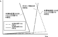
- 4 is a graph showing withstand voltage waveforms of the semiconductor device 100 and the semiconductor device 200;
- top one side in a direction parallel to the depth direction of the semiconductor substrate
- bottom One of the two main surfaces of a substrate, layer or other member
- front surface One of the two main surfaces of a substrate, layer or other member
- back surface One of the two main surfaces of a substrate, layer or other member.
- the directions of “up” and “down” are not limited to the direction of gravity or the direction when the semiconductor device is mounted.
- the Cartesian coordinate axes only specify the relative positions of the components and do not limit any particular orientation.
- the Z axis does not limit the height direction with respect to the ground.
- the +Z-axis direction and the ⁇ Z-axis direction are directions opposite to each other.
- the Z-axis direction is described without indicating positive or negative, it means the +Z-axis and the direction parallel to the Z-axis.
- orthogonal axes parallel to the front and back surfaces of the semiconductor substrate are defined as the X-axis and the Y-axis.
- the axis perpendicular to the front and back surfaces of the semiconductor substrate is defined as the Z-axis.
- the Z-axis direction may be referred to as the depth direction.
- the direction parallel to the front and back surfaces of the semiconductor substrate, including the X-axis and Y-axis, is sometimes referred to as the horizontal direction.
- the conductivity type of the doping region doped with impurities is described as P-type or N-type.
- an impurity may specifically refer to either an N-type donor or a P-type acceptor, and may be referred to as a dopant.
- doping means introducing donors or acceptors into a semiconductor substrate to make it a semiconductor exhibiting N-type conductivity or a semiconductor exhibiting P-type conductivity.
- doping concentration means the concentration of donors or the concentration of acceptors at thermal equilibrium.
- the net doping concentration means the net concentration including charge polarity, where the donor concentration is the positive ion concentration and the acceptor concentration is the negative ion concentration.
- the donor concentration is N D and the acceptor concentration is N A , then the net net doping concentration at any location is N D ⁇ N A.
- a donor has the function of supplying electrons to a semiconductor.
- the acceptor has the function of receiving electrons from the semiconductor.
- Donors and acceptors are not limited to impurities per se. For example, VOH defects in which vacancies (V), oxygen (O), and hydrogen (H) are combined in semiconductors function as donors that supply electrons.
- references herein to P-type or N-type refer to higher doping concentrations than P-type or N-type; references to P-type or N-type refer to higher doping than P-type or N-type. It means that the concentration is low.
- the term P++ type or N++ type in this specification means that the doping concentration is higher than that of the P+ type or N+ type.
- chemical concentration refers to the concentration of impurities measured regardless of the state of electrical activation. Chemical concentrations can be measured, for example, by secondary ion mass spectroscopy (SIMS).
- the net doping concentrations mentioned above can be measured by the voltage-capacitance method (CV method).
- the carrier concentration measured by the spreading resistance measurement method (SR method) may be used as the net doping concentration.
- the carrier concentration measured by the CV method or SR method may be a value in thermal equilibrium.
- the carrier concentration in the region may be used as the donor concentration.
- the carrier concentration in that region may be used as the acceptor concentration.
- the peak value may be the concentration of donors, acceptors, or net doping in the region.
- the average value of the concentration of donors, acceptors or net doping in the region may be used as the concentration of donors, acceptors or net doping.
- the carrier concentration measured by the SR method may be lower than the donor or acceptor concentration.
- the carrier mobility of the semiconductor substrate may be lower than the value in the crystalline state. A decrease in carrier mobility is caused by scattering of carriers due to disorder of the crystal structure due to lattice defects or the like.
- the donor or acceptor concentration calculated from the carrier concentration measured by the CV method or the SR method may be lower than the chemical concentration of the element representing the donor or acceptor.
- the donor concentration of phosphorus or arsenic as a donor or the acceptor concentration of boron (boron) as an acceptor in a silicon semiconductor is about 99% of these chemical concentrations.
- the donor concentration of hydrogen serving as a donor in a silicon semiconductor is about 0.1% to 10% of the chemical concentration of hydrogen.
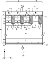
- FIG. 1 is a diagram showing an example of the top surface of a semiconductor device 100 according to this embodiment.
- FIG. 1 shows the positions of each member projected onto the front surface of the semiconductor substrate 10 .
- FIG. 1 only some members of the semiconductor device 100 are shown, and some members are omitted.
- a semiconductor device 100 includes a semiconductor substrate 10 .
- the semiconductor substrate 10 has an edge 102 when viewed from above.
- simply referring to a top view means viewing from the front surface side of the semiconductor substrate 10 .
- the semiconductor substrate 10 of this example has two sets of edges 102 facing each other when viewed from above.
- the X-axis and Y-axis are parallel to one of the edges 102 .
- the Z-axis is perpendicular to the front surface of the semiconductor substrate 10 .
- An active portion 160 is provided on the semiconductor substrate 10 .
- the active portion 160 is a region through which a main current flows in the depth direction between the front surface and the back surface of the semiconductor substrate 10 when the semiconductor device 100 operates.
- An emitter electrode is provided above the active portion 160, but is omitted in FIG.
- At least one of a transistor section 70 including a transistor element such as an IGBT and a diode section 80 including a diode element such as a freewheeling diode (FWD) is provided in the active section 160 .
- the transistor portions 70 and the diode portions 80 are alternately arranged along a predetermined arrangement direction (X-axis direction in this example) on the front surface of the semiconductor substrate 10 .
- the region where the transistor section 70 is arranged is denoted by the symbol "I”
- the region where the diode section 80 is arranged is denoted by the symbol "F”.
- the direction perpendicular to the arrangement direction in top view may be referred to as the stretching direction (the Y-axis direction in FIG. 1).
- the transistor section 70 and the diode section 80 may each have a length in the extending direction. That is, the length in the Y-axis direction of the transistor section 70 is greater than the width in the X-axis direction. Similarly, the length in the Y-axis direction of the diode section 80 is greater than the width in the X-axis direction.
- the extending direction of the transistor portion 70 and the diode portion 80 may be the same as the longitudinal direction of each trench portion described later.
- the transistor section 70 has a P+ type collector region in a region in contact with the back surface of the semiconductor substrate 10 .
- the diode section 80 has an N+ type cathode region in a region in contact with the back surface of the semiconductor substrate 10 .
- the region provided with the collector region is referred to as a transistor section 70 . That is, the transistor portion 70 is a region that overlaps with the collector region when viewed from above.
- An N+ type cathode region may be provided on the back surface of the semiconductor substrate 10 in a region other than the collector region.
- a cathode region is provided on the lower surface of an extension region extending in the Y-axis direction from the transistor section 70 to a gate runner, which will be described later.
- the extension region is included in diode section 80 .
- a gate structure having an N-type emitter region, a P-type base region, a gate conductive portion and a gate insulating film is periodically arranged on the front surface side of the semiconductor substrate 10 .
- the semiconductor device 100 may have one or more pads above the semiconductor substrate 10 .
- the semiconductor device 100 shown in FIG. 1 has a gate pad G, but this is for illustration only.
- Semiconductor device 100 may have pads such as an anode pad, a cathode pad, and a current sensing pad. Each pad is arranged near the edge 102 . The vicinity of the edge 102 refers to a region between the edge 102 and the emitter electrode in top view. When the semiconductor device 100 is mounted, each pad may be connected to an external circuit via a wiring such as a wire.
- a gate potential is applied to the gate pad G.
- the gate pad G is electrically connected to the conductive portion of the gate trench portion of the active portion 160 .
- the semiconductor device 100 includes a gate runner 48 electrically connecting the gate pad G and the gate trench portion.
- the gate runner 48 is arranged between the active portion 160 and the edge 102 of the semiconductor substrate 10 when viewed from above.
- the gate runner 48 of this example surrounds the active portion 160 in top view.
- a region surrounded by the gate runners 48 in top view may be the active portion 160 .
- the gate runners 48 are arranged above the semiconductor substrate 10 .
- the gate runners 48 of this example may be formed of impurity-doped polysilicon or the like.
- the gate runner 48 is electrically connected to a gate conductive portion provided inside the gate trench portion via a gate insulating film.
- the semiconductor device 100 of this example includes a breakdown voltage structure portion 190 provided on the outer periphery of the active portion 160 .
- the breakdown voltage structure 190 of this example is arranged between the gate runner 48 and the edge 102 .
- the breakdown voltage structure 190 relaxes electric field concentration on the front surface side of the semiconductor substrate 10 .
- the pressure resistant structure 190 may have a guard ring 92 .
- Guard ring 92 is a P-type region in contact with the front surface of semiconductor substrate 10 .
- the withstand voltage structure 190 of this example has a plurality of guard rings 92, only one guard ring 92 is shown in FIG.
- the breakdown voltage structure 190 may further include at least one of a field plate and a resurf provided in an annular shape surrounding the active portion 160 .
- the semiconductor device 100 also includes a temperature sensing portion (not shown), which is a PN junction diode made of polysilicon or the like, and a current detecting portion (not shown) that operates in the same manner as the transistor portion provided in the active portion 160.
- a temperature sensing portion (not shown), which is a PN junction diode made of polysilicon or the like, and a current detecting portion (not shown) that operates in the same manner as the transistor portion provided in the active portion 160.
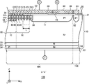
- FIG. 2A is an enlarged view showing an example of the top surface of the semiconductor device 100.
- FIG. FIG. 2A shows region A shown in FIG.
- the semiconductor device 100 includes a semiconductor substrate having a transistor section 70 including transistor elements such as IGBTs and a diode section 80 including diode elements such as a freewheeling diode (FWD).
- transistor elements such as IGBTs
- diode section 80 including diode elements such as a freewheeling diode (FWD).
- FWD freewheeling diode
- the transistor sections 70 and the diode sections 80 of this example are alternately arranged along the arrangement direction (the X-axis direction in this example).
- the diode section 80 is provided between the transistor section 70 adjacent to the withstand voltage structure section 190 and the withstand voltage structure section 190 when viewed from above. That is, the diode section 80 is arranged on the outermost side of the active section 160 .
- inside and outside means that the direction toward the center of the semiconductor device 100 is the inside, and the direction away from the center is the outside.
- a semiconductor device 100 of this example includes a gate trench portion 40, a dummy trench portion 30, a well region 11, an emitter region 12, a base region 14, and a contact region 15 provided on the front surface side of a semiconductor substrate.
- Each of the gate trench portion 40 and the dummy trench portion 30 is an example of the trench portion.
- the semiconductor device 100 of this example also includes a gate metal layer 50 and an emitter electrode 52 provided above the front surface of the semiconductor substrate. Gate metal layer 50 and emitter electrode 52 are provided separately from each other. Gate metal layer 50 and emitter electrode 52 are electrically insulated.
- An interlayer insulating film is provided between the emitter electrode 52 and the gate metal layer 50 and the front surface of the semiconductor substrate, but is omitted in FIG. 2A.
- Contact holes 49, 54 and 56 are provided through the interlayer insulating film of this example. In FIG. 2A, each contact hole is hatched with oblique lines.
- the emitter electrode 52 is provided above the gate trench portion 40 , the dummy trench portion 30 , the well region 11 , the emitter region 12 , the base region 14 and the contact region 15 .
- Emitter electrode 52 is electrically connected to emitter region 12 , base region 14 and contact region 15 on the front surface of the semiconductor substrate through contact hole 54 .
- the emitter electrode 52 is connected to the dummy conductive portion in the dummy trench portion 30 through a contact hole 56 .
- a connection portion 25 made of a conductive material such as impurity-doped polysilicon may be provided between the emitter electrode 52 and the dummy conductive portion.
- the connection portion 25 is provided on the front surface of the semiconductor substrate via an insulating film such as an interlayer insulating film and a dummy insulating film of the dummy trench portion 30 .
- the gate metal layer 50 is electrically connected with the gate runner 48 through the contact hole 49 .
- the gate runners 48 may be made of impurity-doped polysilicon or the like. Gate runners 48 connect to gate conductors within gate trenches 40 on the front surface of the semiconductor substrate. Gate runners 48 are not electrically connected to dummy conductive portions in dummy trench portion 30 and emitter electrode 52 .
- the gate runner 48 and the emitter electrode 52 are electrically separated by an insulator such as an interlayer insulating film and an oxide film.
- the gate runner 48 of this example is provided from below the contact hole 49 to the tip of the gate trench portion 40 .
- the gate conductive portion is exposed to the front surface of the semiconductor substrate at the tip portion of the gate trench portion 40 and is connected to the gate runner 48 .
- the emitter electrode 52 and the gate metal layer 50 are made of a conductive material containing metal.
- a conductive material containing metal For example, it is made of aluminum or an alloy containing aluminum as a main component (for example, an aluminum-silicon alloy).
- Each electrode may have a barrier metal made of titanium, a titanium compound, or the like under a region made of aluminum or the like.
- Each electrode may have a plug made of tungsten or the like in the contact hole.
- the plug may have a barrier metal on the side in contact with the semiconductor substrate, embed tungsten so as to be in contact with the barrier metal, and be formed of aluminum or the like on the tungsten.
- a plug is provided in a contact hole in contact with the contact region 15 or the base region 14 .
- a P++ type plug region is formed under the contact hole of the plug, and has a higher doping concentration than the contact region 15 . This can improve the contact resistance between the barrier metal and contact region 15 .
- the depth of the plug region is approximately 0.1 ⁇ m or less, and has a small region of 10% or less of the depth of the contact region 15 .
- the plug area has the following features.
- the latch-up resistance is improved by improving the contact resistance.
- the contact resistance between the barrier metal and the base region 14 is high, and conduction loss and switching loss increase. An increase in switching loss can be suppressed.
- the well region 11 overlaps the gate runner 48, extends the outer periphery of the active portion 160, and is provided in a ring shape when viewed from above.
- the well region 11 extends with a predetermined width even in a range that does not overlap with the gate runner 48, and is provided in an annular shape when viewed from above.
- the well region 11 of this example is provided away from the Y-axis direction end of the contact hole 54 on the gate runner 48 side.
- the well region 11 is a second conductivity type region having a higher doping concentration than the base region 14 .
- Gate runner 48 is electrically insulated from well region 11 .
- the base region 14 in this example is of P ⁇ type, and the well region 11 is of P+ type. Also, the well region 11 is formed from the front surface of the semiconductor substrate to a position deeper than the lower end of the base region 14 . Base region 14 is provided in contact with well region 11 in transistor section 70 and diode section 80 . Therefore, well region 11 is electrically connected to emitter electrode 52 .
- Each of the transistor section 70 and the diode section 80 has a plurality of trench sections arranged in the arrangement direction.
- One or more gate trench portions 40 are provided in the transistor portion 70 of this example along the arrangement direction.
- a plurality of dummy trench portions 30 are provided along the array direction in the diode portion 80 of this example.
- the gate trench portion 40 is not provided in the diode portion 80 of this example.
- the gate trench portion 40 of this example connects the two straight portions 39 extending along the extending direction perpendicular to the arrangement direction (the portion of the trench that is linear along the extending direction) and the two straight portions 39 . It may have a tip 41 .
- At least part of the tip portion 41 may be provided in a curved shape when viewed from above.
- the tip portion 41 functions as a gate electrode to the gate trench portion 40 .
- electric field concentration at the end portion can be alleviated as compared with the case where the tip portion 41 is completed with the straight portion 39 .
- the transistor section 70 may be alternately provided with one or more gate trench sections 40 and one or more dummy trench sections 30 along the arrangement direction.
- the dummy trench portions 30 are provided between the respective straight portions 39 of the gate trench portion 40 .
- One dummy trench portion 30 may be provided between the straight portions 39, or a plurality of dummy trench portions 30 may be provided.
- the dummy trench portions 30 may not be provided, and the gate trench portions 40 may be provided. With such a structure, the electron current from the emitter region 12 can be increased, thereby reducing the ON voltage.
- the dummy trench portion 30 may have a linear shape extending in the extending direction, and may have a linear portion 29 and a tip portion 31 like the gate trench portion 40 .
- the semiconductor device 100 shown in FIG. 2A only the dummy trench portions 30 having the tip portions 31 are arranged. A portion 30 may be included.
- the diffusion depth of the well region 11 may be deeper than the depths of the gate trench portion 40 and the dummy trench portion 30 .
- Y-axis direction ends of the gate trench portion 40 and the dummy trench portion 30 are provided in the well region 11 when viewed from above. That is, the bottom of each trench in the depth direction is covered with the well region 11 at the end of each trench in the Y-axis direction. Also, the trench portion provided at the end in the X-axis direction may be covered with the well region 11 . As a result, electric field concentration at the bottom of each trench can be relaxed.
- a mesa portion is provided between each trench portion in the arrangement direction.
- the mesa portion refers to a region sandwiched between trench portions inside the semiconductor substrate.
- the depth position of the mesa portion is from the front surface of the semiconductor substrate to the lower end of the trench portion.
- the mesa portion of this example is sandwiched between adjacent trench portions in the X-axis direction, and is provided extending in the extension direction (Y-axis direction) along the trenches on the front surface of the semiconductor substrate.
- the transistor section 70 is provided with a mesa section 60 and the diode section 80 is provided with a mesa section 61 .
- simply referring to the mesa portion refers to the mesa portion 60 and the mesa portion 61 respectively.
- a base region 14 is provided in each mesa portion.
- at least one of the first conductivity type emitter region 12 and the second conductivity type contact region 15 may be provided in a region sandwiched between the base regions 14 in top view.
- the emitter region 12 in this example is of N+ type and the contact region 15 is of P+ type.
- Emitter region 12 and contact region 15 may be provided between base region 14 and the front surface of the semiconductor substrate in the depth direction.
- the mesa portion of the transistor portion 70 has the emitter region 12 exposed on the front surface of the semiconductor substrate.
- the emitter region 12 is provided in contact with the gate trench portion 40 .
- a contact region 15 exposed on the front surface of the semiconductor substrate is provided in the mesa portion in contact with the gate trench portion 40 .
- Each of the contact region 15 and the emitter region 12 in the mesa portion is provided from one trench portion to the other trench portion in the X-axis direction.
- the contact regions 15 and the emitter regions 12 of the mesa are alternately arranged along the extending direction (Y-axis direction) of the trench.
- the contact regions 15 and the emitter regions 12 of the mesa portion may be provided in stripes along the extension direction (Y-axis direction) of the trench portion.
- an emitter region 12 is provided in a region in contact with the trench portion, and a contact region 15 is provided in a region sandwiched between the emitter regions 12 .
- the mesa portion of the diode portion 80 is not provided with the emitter region 12 .
- a base region 14 may be provided on the upper surface of the mesa portion of the diode portion 80 .
- the base region 14 may be arranged over the mesa portion of the diode portion 80 .
- a contact hole 54 is provided above each mesa portion.
- the contact hole 54 is arranged in a region sandwiched between the base regions 14 in its extending direction (Y-axis direction).
- the contact hole 54 of this example is provided above each region of the contact region 15 , the base region 14 and the emitter region 12 .
- the contact hole 54 may be arranged in the center in the arrangement direction (X-axis direction) of the mesa portions.
- an N+ type cathode region 82 is provided in a region adjacent to the back surface of the semiconductor substrate.
- a P+ type collector region 22 may be provided in a region where the cathode region 82 is not provided on the back surface of the semiconductor substrate.
- the boundary between cathode region 82 and collector region 22 is indicated by a dashed line.
- an N+ type cathode region 82 may be provided on the back side of the semiconductor substrate.
- FIG. 2B is a diagram showing the aa' cross section in FIG. 2A.
- the aa′ cross section is the XZ plane passing through the contact region 15 , the base region 14 , the gate trench portion 40 and the dummy trench portion 30 .
- a semiconductor device 100 of this example has a semiconductor substrate 10, an interlayer insulating film 38, an emitter electrode 52 and a collector electrode 24 in the aa' section.
- the interlayer insulating film 38 is provided on the front surface 21 of the semiconductor substrate 10 .
- the interlayer insulating film 38 is an insulating film such as silicate glass doped with an impurity such as boron or phosphorus. Interlayer insulating film 38 may be in contact with front surface 21 , and another film such as an oxide film may be provided between interlayer insulating film 38 and front surface 21 .
- the interlayer insulating film 38 is provided with the contact holes 54 described with reference to FIG. 2A.
- the emitter electrode 52 is provided on the front surface 21 of the semiconductor substrate 10 and the top surface of the interlayer insulating film 38 .
- Emitter electrode 52 is electrically connected to front surface 21 through contact hole 54 in interlayer insulating film 38 .
- a plug region 17 made of tungsten (W) or the like may be provided inside the contact hole 54 .
- Collector electrode 24 is provided on back surface 23 of semiconductor substrate 10 .
- Emitter electrode 52 and collector electrode 24 are made of a material containing metal or a laminated film thereof.
- the semiconductor substrate 10 may be a silicon substrate, a silicon carbide substrate, a nitride semiconductor substrate such as gallium nitride, or the like.
- the semiconductor substrate 10 of this example is a silicon substrate.
- the semiconductor substrate 10 has a first conductivity type drift region 18 .
- the drift region 18 in this example is of the N ⁇ type.
- Drift region 18 may be a remaining region of semiconductor substrate 10 that is not provided with other doping regions.
- one or more accumulation regions 16 may be provided above the drift region 18 in the Z-axis direction.
- the accumulation region 16 is a region in which the same dopant as the drift region 18 is accumulated at a higher concentration than the drift region 18 .
- the doping concentration of accumulation region 16 is higher than the doping concentration of drift region 18 .
- the accumulation region 16 in this example is of N type.
- the accumulation region 16 may be provided between the base region 14 and a trench bottom portion 75 described later in the transistor portion 70 .
- the accumulation region 16 may be provided only in the transistor section 70 or may be provided in both the transistor section 70 and the diode section 80 .
- an emitter region 12 is provided above the base region 14 and in contact with the front surface 21 .
- Emitter region 12 is provided in contact with gate trench portion 40 .
- the doping concentration of emitter region 12 is higher than the doping concentration of drift region 18 .
- the dopant for the emitter region 12 is, for example, arsenic (As), phosphorus (P), antimony (Sb), or the like.
- the diode section 80 is provided with the base region 14 exposed on the front surface 21 .
- Base region 14 of diode section 80 acts as an anode.
- a buffer region 20 of the first conductivity type may be provided below the drift region 18 .
- the buffer region 20 in this example is of N type.
- the doping concentration of buffer region 20 is higher than the doping concentration of drift region 18 .
- Buffer region 20 may function as a field stop layer that prevents a depletion layer extending from the lower surface side of base region 14 from reaching collector region 22 and cathode region 82 .
- a collector region 22 is provided below the buffer region 20 in the transistor section 70 .
- Collector region 22 may be provided in contact with cathode region 82 on rear surface 23 .
- a cathode region 82 is provided below the buffer region 20 in the diode section 80 .
- the cathode region 82 may be provided at the same depth as the collector region 22 of the transistor section 70 .
- the diode section 80 may function as a freewheeling diode (FWD) that allows a freewheeling current to flow in the opposite direction when the transistor section 70 is turned off.
- FWD freewheeling diode
- a gate trench portion 40 and a dummy trench portion 30 are provided in the semiconductor substrate 10 . Gate trench portion 40 and dummy trench portion 30 are provided to reach drift region 18 through base region 14 and accumulation region 16 from front surface 21 .
- the fact that the trench penetrates the doping region is not limited to the order of forming the doping region and then forming the trench.
- a structure in which a doping region is formed between the trench portions after the trench portions are formed is also included in the structure in which the trench portion penetrates the doping regions.
- the gate trench portion 40 has a gate trench provided in the front surface 21, a gate insulating film 42 and a gate conductive portion 44.
- a gate insulating film 42 is provided to cover the inner wall of the gate trench.
- the gate insulating layer 42 may be formed of an oxide layer or a nitride layer.
- the gate conductive portion 44 is provided so as to fill the gate insulating film 42 inside the gate trench.
- the top surface of the gate conductive portion 44 may be in the same XY plane as the front surface 21 .
- the gate insulating film 42 insulates the gate conductive portion 44 from the semiconductor substrate 10 .
- the gate conductive portion 44 is formed of impurity-doped polysilicon or the like.
- the gate conductive portion 44 may be provided longer than the base region 14 in the depth direction. Gate trench portion 40 is covered with interlayer insulating film 38 on front surface 21 . When a predetermined voltage is applied to the gate conductive portion 44, a channel is formed by an electron inversion layer in the surface layer of the interface of the base region 14 in contact with the gate trench.
- the dummy trench portion 30 may have the same structure as the gate trench portion 40 in the XZ cross section.
- the dummy trench portion 30 has dummy trenches provided in the front surface 21 , a dummy insulating film 32 and a dummy conductive portion 34 .
- a dummy insulating film 32 is provided to cover the inner wall of the dummy trench.
- the dummy insulating film 32 may be formed of an oxide film or a nitride film.
- the dummy conductive portion 34 is provided so as to fill the inner side of the dummy insulating film 32 inside the dummy trench.
- the top surface of the dummy conductive portion 34 may be on the same XY plane as the front surface 21 .
- the dummy insulating film 32 insulates the dummy conductive portion 34 from the semiconductor substrate 10 .
- the dummy conductive portion 34 may be made of the same material as the gate conductive portion 44 .
- the gate trench portion 40 and the dummy trench portion 30 of this example are covered with an interlayer insulating film 38 on the front surface 21 .
- the bottoms of the dummy trench portion 30 and the gate trench portion 40 may be curved (curved in cross section) convex downward.
- the transistor section 70 has a P-type trench bottom section 75 provided at the lower end of the trench section.
- the trench bottom portion 75 of this example is provided below the accumulation region 16 .
- the lower end of the trench bottom portion 75 may be positioned below the bottom portion of the gate trench portion 40 .
- the trench bottom portion 75 may cover the bottom portion of the gate trench portion 40 .
- the doping concentration of trench bottom portion 75 is greater than the doping concentration of drift region 18 and less than the doping concentration of base region 14 .
- the doping concentration of the trench bottom portion 75 is 1E12 cm ⁇ 3 or more and 1E13 cm ⁇ 3 or less.
- the end of the trench bottom portion 75 on the positive side in the X-axis direction coincides with the boundary between the cathode region 82 and the collector region 22, but extends further toward the diode portion 80 side. It may be recessed into the transistor portion 70 .
- the trench bottom portion 75 may be an electrically floating floating layer.
- a floating layer refers to a layer that is not electrically connected to any electrode such as the emitter electrode 52 .
- FIG. 2C is a diagram showing a bb' section in FIG. 2A.
- the bb' section is the XZ plane passing through the emitter region 12, the contact region 15, the base region 14, the gate trench portion 40 and the dummy trench portion 30 in the vicinity of the boundary between the active portion 160 and the breakdown voltage structure portion 190.
- the diode section 80 of this example is provided between the transistor section 70 adjacent to the withstand voltage structure section 190 and the withstand voltage structure section 190 when viewed from above. In other words, the diode section 80 is arranged closest to the breakdown voltage structure section 190 side of the active section 160 .
- the transistor section 70 of this example has the trench bottom section 75 .
- the trench bottom portion 75 is not provided in part of the transistor portion 70, and the trench bottom portion 75 is separated from the well region 11 electrically connected to the emitter electrode 52.
- the transistor portion 70 if the trench bottom portion 75 is not provided in a certain range from the end portion on the side of the withstanding voltage structure portion 190, the turn-on characteristics are degraded according to the amount of decrease in the trench bottom portion 75.
- the trench bottom section 75 can be provided in the entire transistor section 70, so that turn-on characteristics can be improved.
- the breakdown voltage of the transistor portion 70 is improved.
- the breakdown voltage of the semiconductor device 100 as a whole is improved, and the latch-up resistance is improved.
- the well region 11 is separated from the emitter electrode 52 .
- the well region 11 and the emitter electrode 52 can be insulated by providing the interlayer insulating film 38 between the well region 11 and the emitter electrode 52 .
- the interlayer insulating film 38 extends from the breakdown voltage structure 190 over part of the diode section 80 provided on the outermost side of the active section 160 when viewed from above.
- the distance L between the edge of the interlayer insulating film 38 and the edge of the well region 11 may be 10 ⁇ m or more and 30 ⁇ m or less.
- the transistor portion 70 has an N-type accumulation region 16 between the base region 14 and the trench bottom portion 75 .
- the accumulation region 16 may be provided only in the transistor section 70 and not provided in the diode section 80 .
- the accumulation region 16 may be provided in both the transistor section 70 and the diode section 80 .
- the effect of accelerating injection of carriers (IE effect) can be enhanced and the ON voltage can be reduced.
- An N-type cathode region 82 may be provided on the back surface 23 side of the semiconductor substrate 10 in the breakdown voltage structure 190 . That is, the cathode region 82 may be continuously provided on the back surface 23 side of the semiconductor substrate 10 from the diode portion 80 to the breakdown voltage structure portion 190 so as to surround the outer periphery of the active portion 160 .
- FIG. 2D is a diagram showing a cc' section in FIG. 2A.
- the cc' section is the YZ plane passing through the base region 14 and the contact region 15 provided in the diode section 80 in the vicinity of the Y-axis negative side end of the active section 160 .
- the diode section 80 is provided on the outermost side of the active section 160 .
- the contact region 15 is provided on the front surface 21 of the semiconductor substrate 10 .
- the base region 14 is exposed to the front surface 21 of the semiconductor substrate 10 outside the contact region 15 in the Y-axis direction. That is, when viewed from above, in the diode section 80, the contact region 15 is sandwiched between the base regions 14 in the Y-axis direction.
- a well region 11 is provided in the vicinity of the Y-axis negative side end of the active portion 160 .
- the diffusion depth of well region 11 is deeper than base region 14 .
- the well region 11 may extend in the Y-axis direction so as to partially cover the bottom of the base region 14 .
- FIG. 2E is a diagram showing a dd' cross section in FIG. 2A.
- the dd' section is the YZ plane passing through the emitter region 12, the base region 14 and the contact region 15 provided in the transistor section 70 in the vicinity of the Y-axis negative side end of the active section 160.
- FIG. The dd' cross section passes through an extension region extending the transistor portion 70 in the Y-axis direction.
- a cathode region is provided on the underside of the extension region. That is, when viewed from above, the transistor section 70 is sandwiched between the diode sections 80 in the Y-axis direction.
- the emitter region 12 and the contact region 15 are provided on the front surface 21 of the semiconductor substrate 10 .
- the base region 14 is exposed to the front surface 21 of the semiconductor substrate 10 outside the contact region 15 in the Y-axis direction.
- the emitter region 12 and the contact region 15 are sandwiched between the base regions 14 in the Y-axis direction.
- An accumulation region 16 and a trench bottom portion 75 are provided above the drift region 18 in the transistor portion 70 .
- the trench bottom portion 75 is provided below the accumulation region 16 .
- the trench bottom portion 75 may be provided in contact with the bottom surface of the accumulation region 16 .
- FIG. 2F is a diagram showing another example of the aa' cross section in FIG. 2A.
- the aa' cross section is the XZ plane passing through the contact region 15, the base region 14, the gate trench portion 40 and the dummy trench portion 30 as in FIG. 2B.
- a semiconductor device 100 of this example has a semiconductor substrate 10, an interlayer insulating film 38, an emitter electrode 52 and a collector electrode 24 in the aa' section.
- the lower end of the trench bottom portion 75 in this example is located below the bottom portion of the gate trench portion 40 and covers the bottom portion of the gate trench portion 40 .
- the trench bottom portion 75 may be an electrically floating floating layer.
- the end portion of the trench bottom portion 75 on the positive side in the X-axis direction coincides with the boundary between the cathode region 82 and the collector region 22, but extends toward the diode portion 80 side. It may be recessed into the transistor portion 70 . This example can obtain the same effect as in FIG. 2B.
- FIG. 2G is a diagram showing another example of the aa' cross section in FIG. 2A.
- the aa' cross section is the XZ plane passing through the contact region 15, the base region 14, the gate trench portion 40 and the dummy trench portion 30 as in FIG. 2B.
- a semiconductor device 100 of this example has a semiconductor substrate 10, an interlayer insulating film 38, an emitter electrode 52 and a collector electrode 24 in the aa' section.
- FIG. 1 is provided apart from the accumulation region 16, that is, the drift region 18 is interposed between the accumulation region 16 and the trench bottom portion 75.
- the trench bottom portion 75 may be thinner than the accumulation region 16 or the drift region 18 between the accumulation region 16 and the trench bottom portion 75 in the depth direction of the semiconductor substrate 10 .
- the end of the trench bottom portion 75 on the positive side in the X-axis direction coincides with the boundary between the cathode region 82 and the collector region 22, but extends further toward the diode portion 80 side. It may be recessed into the transistor portion 70 . This example can obtain the same effect as in FIG. 2B.
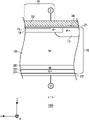
- FIG. 3A is an enlarged view showing an example of the top surface of a semiconductor device 200 according to a comparative example. Similar to FIG. 2A, FIG. 3A shows the region A shown in FIG. In the semiconductor device 200, members common to those in the semiconductor device 100 are denoted by the same reference numerals.
- the transistor section 70 of the semiconductor device 200 is provided between the diode section 80 adjacent to the withstand voltage structure section 190 and the withstand voltage structure section 190 in top view. That is, unlike FIG. 2A, the transistor section 70 is arranged on the outermost side of the active section 160 . A contact hole 54 is provided above the well region 11 . Therefore, well region 11 is electrically connected to emitter electrode 52 (not shown).
- FIG. 3B is a diagram showing the ee' section in FIG. 3A.
- the ee' section is the XZ plane passing through the emitter region 12, the contact region 15, the base region 14, the gate trench portion 40 and the dummy trench portion 30.
- FIG. 3B is a diagram showing the ee' section in FIG. 3A.
- the ee' section is the XZ plane passing through the emitter region 12, the contact region 15, the base region 14, the gate trench portion 40 and the dummy trench portion 30.
- the transistor section 70 is arranged on the outermost side of the active section 160 .
- a P-type collector region 22 is provided on the back surface 23 side of the semiconductor substrate 10 . That is, the collector region 22 is continuously provided on the back surface 23 side of the semiconductor substrate 10 from the transistor portion 70 to the breakdown voltage structure portion 190 .
- the transistor section 70 of the semiconductor device 200 has a trench bottom section 75 . However, if the trench bottom portion 75 is provided in the entire transistor portion 70 provided on the outermost side of the active portion 160 , the trench bottom portion 75 contacts the well region 11 . Since the well region 11 is electrically connected to the emitter electrode 52, the trench bottom portion 75 is fixed at the emitter potential and current cannot flow.
- the trench bottom section 75 is not provided on the side of the breakdown voltage structure section 190 . This separates the trench bottom portion 75 from the well region 11 electrically connected to the emitter electrode 52 . Therefore, since the semiconductor device 200 has a smaller trench bottom portion 75 than the semiconductor device 100, the turn-on characteristics are degraded according to the difference. Also, the withstand voltage of the semiconductor device 200 is lower than that of the semiconductor device 100, and the latch-up resistance is lowered.
- FIG. 4 is a graph showing breakdown voltage waveforms of the semiconductor device 100 and the semiconductor device 200.
- the breakdown voltage of a device is determined by the breakdown voltage of the trench bottom where current tends to concentrate. Since the IGBT has a negative resistance, as the current Ic increases, the voltage Vce decreases and the current concentrates in the same place, such as the bottom of the trench. On the other hand, the FWD does not concentrate the current in one place because the voltage increases as the current Ic increases.
- the breakdown voltage of the IGBT is lower than that of the FWD, the breakdown voltage of the RC-IGBT is determined by the breakdown voltage of the FWD. Due to the influence of the parasitic thyristor inherent in the IGBT, there is a risk of latch-up when avalanche occurs due to current concentration. On the other hand, since the FWD does not have a parasitic thyristor, there is no risk of latch-up even if avalanche occurs due to current concentration.
- the solid line indicates the breakdown voltage waveform of the transistor section 70 of the semiconductor device 200
- the dashed-dotted line indicates the breakdown voltage waveform of the diode section 80.
- the breakdown voltage of the transistor section 70 is lower than that of the diode section 80 , so the breakdown voltage of the semiconductor device 200 is determined by the breakdown voltage of the transistor section 70 .
- the transistor portion 70 of the semiconductor device 100 is entirely provided with the trench bottom portion 75, so that the breakdown voltage is higher than that of the transistor portion 70 of the semiconductor device 200 according to the difference. rises.
- a dashed line indicates a breakdown voltage waveform of the transistor section 70 of the semiconductor device 100 .
- the breakdown voltage waveform of the transistor portion 70 of the semiconductor device 100 is parallel shifted to the right by the amount of the breakdown voltage increase from the breakdown voltage waveform of the transistor portion 70 of the semiconductor device 200 .
- the withstand voltage of the diode portion 80 of the semiconductor device 100 is the same as that of the semiconductor device 200 .
- the breakdown voltage of the transistor section 70 is higher than that of the diode section 80 , so the breakdown voltage of the semiconductor device 100 is determined by the breakdown voltage of the diode section 80 .
- the breakdown voltage waveform of the semiconductor device 100 follows the one-dot chain line in FIG.
- the breakdown voltage waveform of the semiconductor device 200 follows the solid line in FIG. In this way, the breakdown voltage of the semiconductor device 100 is higher than that of the semiconductor device 200, and even if avalanche occurs in the diode section 80, there is no fear of latch-up, so the avalanche resistance is improved.
- connection part 29 Straight portion 30 Dummy trench portion 31 Tip portion 32 Dummy insulating film 34 Dummy conductive portion 38 Interlayer insulating film 39 Straight line Part 40 Gate trench portion 41 Tip portion 42 Gate insulating film 44 Gate conductive portion 48 Gate runner 49 Contact hole 50 Gate metal layer 52 Emitter electrode 54 Contact hole 56 Contact hole 60 Mesa portion 61 Mesa portion 70 Transistor portion 75 Trench bottom portion 80 Diode portion 82 Cathode region 92 Guard ring 100 Semiconductor device 102 Edge 160 Active portion 190 ⁇ Breakdown structure part, 200 ... semiconductor device
Abstract
This semiconductor device is provided with an active portion including a transistor portion and a diode portion, and a breakdown voltage structure portion provided at an outer periphery of the active portion, wherein: the transistor portion includes a drift region of a first conduction type, provided in a semiconductor substrate, a base region of a second conduction type, provided above the drift region, a trench portion extending from a front surface of the semiconductor substrate to the drift region, and a trench bottom portion of the second conduction type, provided at a lower end of the trench portion; and the diode portion is provided between the transistor portion in close proximity to the breakdown voltage structure portion and the breakdown voltage structure portion as seen in a top view.
Description
本発明は、半導体装置に関する。
The present invention relates to semiconductor devices.
特許文献1には、IGBTセルの少なくとも一部が、第2の導電型の電気的に浮遊するバリア領域を含むことが記載されている。
[先行技術文献]
[特許文献]
[特許文献1] 特開2019-91892号公報 US Pat. No. 6,200,009 describes that at least a portion of an IGBT cell includes an electrically floating barrier region of a second conductivity type.
[Prior art documents]
[Patent Literature]
[Patent Document 1] JP 2019-91892 A
[先行技術文献]
[特許文献]
[特許文献1] 特開2019-91892号公報 US Pat. No. 6,200,009 describes that at least a portion of an IGBT cell includes an electrically floating barrier region of a second conductivity type.
[Prior art documents]
[Patent Literature]
[Patent Document 1] JP 2019-91892 A
このようなバリア領域が半導体基板に設けられたウェル領域と接していると、ターンオン特性が低下する。
If such a barrier region is in contact with a well region provided on a semiconductor substrate, turn-on characteristics are degraded.
本発明の第1の態様においては、半導体装置を提供する。半導体装置は、トランジスタ部およびダイオード部を有する活性部と、活性部の外周に設けられた耐圧構造部とを備え、トランジスタ部は、半導体基板に設けられた第1導電型のドリフト領域と、ドリフト領域の上方に設けられた第2導電型のベース領域と、半導体基板のおもて面からドリフト領域まで延伸するトレンチ部と、トレンチ部の下端に設けられた第2導電型のトレンチボトム部とを有し、ダイオード部は、上面視において、耐圧構造部に近接するトランジスタ部と、耐圧構造部との間に設けられる。
A first aspect of the present invention provides a semiconductor device. A semiconductor device includes an active portion having a transistor portion and a diode portion, and a breakdown voltage structure portion provided on the periphery of the active portion. a base region of the second conductivity type provided above the region; a trench portion extending from the front surface of the semiconductor substrate to the drift region; and a trench bottom portion of the second conductivity type provided at the lower end of the trench portion. , and the diode section is provided between the transistor section adjacent to the breakdown voltage structure section and the breakdown voltage structure section when viewed from above.
トレンチボトム部は、電気的に浮遊していてよい。
The trench bottom may be electrically floating.
トレンチボトム部のドーピング濃度は、ドリフト領域のドーピング濃度よりも大きく、ベース領域のドーピング濃度よりも小さくてよい。
The doping concentration of the trench bottom may be higher than that of the drift region and lower than that of the base region.
トレンチボトム部のドーピング濃度は、1E12cm-3以上、1E13cm-3以下であってよい。
The doping concentration of the trench bottom may be greater than or equal to 1E12 cm −3 and less than or equal to 1E13 cm −3 .
トレンチボトム部はダイオード部に設けられていなくてよい。
The trench bottom portion does not have to be provided in the diode portion.
半導体装置は、耐圧構造部において、半導体基板の裏面側に第1導電型のカソード領域をさらに備えてよい。
The semiconductor device may further include a cathode region of the first conductivity type on the back surface side of the semiconductor substrate in the breakdown voltage structure.
半導体装置は、活性部において、半導体基板の上方に設けられたエミッタ電極と、
ダイオード部の少なくとも一部から耐圧構造部にわたって、半導体基板に設けられた第2導電型のウェル領域とをさらに備え、ダイオード部において、ウェル領域はエミッタ電極から離間していてよい。 A semiconductor device includes an emitter electrode provided above a semiconductor substrate in an active portion,
A well region of the second conductivity type provided in the semiconductor substrate extending from at least a portion of the diode portion to the breakdown voltage structure portion may be further provided, and the well region may be spaced apart from the emitter electrode in the diode portion.
半導体装置は、半導体基板のおもて面において、ウェル領域を覆う層間絶縁膜をさらに備え、ダイオード部において、層間絶縁膜は、上面視において、ウェル領域よりも10μm以上30μm以下、半導体基板の内側に延伸していてよい。
The semiconductor device further includes an interlayer insulating film covering the well region on the front surface of the semiconductor substrate. It may be stretched to
トランジスタ部は、トレンチボトム部の上方に設けられた第1導電型の蓄積領域をさらに有し、蓄積領域は、ダイオード部には設けられていなくてよい。
The transistor section further has a first conductivity type accumulation region provided above the trench bottom section, and the accumulation region may not be provided in the diode section.
トランジスタ部およびダイオード部は、ドリフト領域の上方に設けられた第1導電型の蓄積領域をさらに有してよい。
The transistor section and the diode section may further have a first conductivity type accumulation region provided above the drift region.
半導体装置は、蓄積領域とトレンチボトム部との間にドリフト領域をさらに備えてよい。
The semiconductor device may further include a drift region between the accumulation region and the trench bottom.
なお、上記の発明の概要は、本発明の特徴の全てを列挙したものではない。また、これらの特徴群のサブコンビネーションもまた、発明となりうる。
It should be noted that the above outline of the invention does not list all the features of the present invention. Subcombinations of these feature groups can also be inventions.
以下、発明の実施の形態を通じて本発明を説明するが、以下の実施形態は請求の範囲にかかる発明を限定するものではない。また、実施形態の中で説明されている特徴の組み合わせの全てが発明の解決手段に必須であるとは限らない。
Although the present invention will be described below through embodiments of the invention, the following embodiments do not limit the invention according to the scope of claims. Also, not all combinations of features described in the embodiments are essential for the solution of the invention.
本明細書においては半導体基板の深さ方向と平行な方向における一方の側を「上」または「おもて」、他方の側を「下」または「裏」と称する。基板、層またはその他の部材の2つの主面のうち、一方の面をおもて面、他方の面を裏面と称する。「上」、「下」の方向は、重力方向または半導体装置の実装時における方向に限定されない。
In this specification, one side in a direction parallel to the depth direction of the semiconductor substrate is called "top" or "front", and the other side is called "bottom" or "back". One of the two main surfaces of a substrate, layer or other member is called the front surface and the other surface is called the back surface. The directions of “up” and “down” are not limited to the direction of gravity or the direction when the semiconductor device is mounted.
本明細書では、X軸、Y軸およびZ軸の直交座標軸を用いて技術的事項を説明する場合がある。直交座標軸は、構成要素の相対位置を特定するに過ぎず、特定の方向を限定するものではない。例えば、Z軸は地面に対する高さ方向を限定して示すものではない。なお、+Z軸方向と-Z軸方向とは互いに逆向きの方向である。正負を記載せず、Z軸方向と記載した場合、+Z軸およびZ軸に平行な方向を意味する。
In this specification, technical matters may be explained using the X-axis, Y-axis and Z-axis orthogonal coordinate axes. The Cartesian coordinate axes only specify the relative positions of the components and do not limit any particular orientation. For example, the Z axis does not limit the height direction with respect to the ground. Note that the +Z-axis direction and the −Z-axis direction are directions opposite to each other. When the Z-axis direction is described without indicating positive or negative, it means the +Z-axis and the direction parallel to the Z-axis.
本明細書では、半導体基板のおもて面および裏面に平行な直交軸をX軸およびY軸とする。また、半導体基板のおもて面および裏面と垂直な軸をZ軸とする。本明細書では、Z軸の方向を深さ方向と称する場合がある。また、本明細書では、X軸およびY軸を含めて、半導体基板のおもて面および裏面に平行な方向を、水平方向と称する場合がある。
In this specification, orthogonal axes parallel to the front and back surfaces of the semiconductor substrate are defined as the X-axis and the Y-axis. Also, the axis perpendicular to the front and back surfaces of the semiconductor substrate is defined as the Z-axis. In this specification, the Z-axis direction may be referred to as the depth direction. In this specification, the direction parallel to the front and back surfaces of the semiconductor substrate, including the X-axis and Y-axis, is sometimes referred to as the horizontal direction.
本明細書において「同一」または「等しい」のように称した場合、製造ばらつき等に起因する誤差を有する場合も含んでよい。当該誤差は、例えば10%以内である。
In this specification, terms such as "identical" or "equal" may include cases where there is an error due to manufacturing variations or the like. The error is, for example, within 10%.
本明細書においては、不純物がドーピングされたドーピング領域の導電型をP型またはN型として説明している。本明細書においては、不純物とは、特にN型のドナーまたはP型のアクセプタの何れかを意味する場合があり、ドーパントと記載する場合がある。本明細書においては、ドーピングとは、半導体基板にドナーまたはアクセプタを導入し、N型の導電型を示す半導体またはP型の導電型を示す半導体とすることを意味する。
In this specification, the conductivity type of the doping region doped with impurities is described as P-type or N-type. As used herein, an impurity may specifically refer to either an N-type donor or a P-type acceptor, and may be referred to as a dopant. As used herein, doping means introducing donors or acceptors into a semiconductor substrate to make it a semiconductor exhibiting N-type conductivity or a semiconductor exhibiting P-type conductivity.
本明細書においては、ドーピング濃度とは、熱平衡状態におけるドナーの濃度またはアクセプタの濃度を意味する。本明細書においては、ネット・ドーピング濃度とは、ドナー濃度を正イオンの濃度とし、アクセプタ濃度を負イオンの濃度として、電荷の極性を含めて足し合わせた正味の濃度を意味する。一例として、ドナー濃度をND、アクセプタ濃度をNAとすると、任意の位置における正味のネット・ドーピング濃度はND-NAとなる。
As used herein, doping concentration means the concentration of donors or the concentration of acceptors at thermal equilibrium. In this specification, the net doping concentration means the net concentration including charge polarity, where the donor concentration is the positive ion concentration and the acceptor concentration is the negative ion concentration. As an example, if the donor concentration is N D and the acceptor concentration is N A , then the net net doping concentration at any location is N D −N A.
ドナーは、半導体に電子を供給する機能を有している。アクセプタは、半導体から電子を受け取る機能を有している。ドナーおよびアクセプタは、不純物自体には限定されない。例えば、半導体中に存在する空孔(V)、酸素(O)および水素(H)が結合したVOH欠陥は、電子を供給するドナーとして機能する。
A donor has the function of supplying electrons to a semiconductor. The acceptor has the function of receiving electrons from the semiconductor. Donors and acceptors are not limited to impurities per se. For example, VOH defects in which vacancies (V), oxygen (O), and hydrogen (H) are combined in semiconductors function as donors that supply electrons.
本明細書においてP+型またはN+型と記載した場合、P型またはN型よりもドーピング濃度が高いことを意味し、P-型またはN-型と記載した場合、P型またはN型よりもドーピング濃度が低いことを意味する。また、本明細書においてP++型またはN++型と記載した場合には、P+型またはN+型よりもドーピング濃度が高いことを意味する。
References herein to P-type or N-type refer to higher doping concentrations than P-type or N-type; references to P-type or N-type refer to higher doping than P-type or N-type. It means that the concentration is low. In addition, the term P++ type or N++ type in this specification means that the doping concentration is higher than that of the P+ type or N+ type.
本明細書において化学濃度とは、電気的な活性化の状態によらずに測定される不純物の濃度を指す。化学濃度は、例えば二次イオン質量分析法(SIMS)により計測できる。上述したネット・ドーピング濃度は、電圧-容量測定法(CV法)により測定できる。また、拡がり抵抗測定法(SR法)により計測されるキャリア濃度を、ネット・ドーピング濃度としてよい。CV法またはSR法により計測されるキャリア濃度は、熱平衡状態における値としてよい。また、N型の領域においては、ドナー濃度がアクセプタ濃度よりも十分大きいので、当該領域におけるキャリア濃度を、ドナー濃度としてもよい。同様に、P型の領域においては、当該領域におけるキャリア濃度を、アクセプタ濃度としてもよい。
In this specification, chemical concentration refers to the concentration of impurities measured regardless of the state of electrical activation. Chemical concentrations can be measured, for example, by secondary ion mass spectroscopy (SIMS). The net doping concentrations mentioned above can be measured by the voltage-capacitance method (CV method). Also, the carrier concentration measured by the spreading resistance measurement method (SR method) may be used as the net doping concentration. The carrier concentration measured by the CV method or SR method may be a value in thermal equilibrium. In addition, since the donor concentration is sufficiently higher than the acceptor concentration in the N-type region, the carrier concentration in the region may be used as the donor concentration. Similarly, in a P-type region, the carrier concentration in that region may be used as the acceptor concentration.
また、ドナー、アクセプタまたはネット・ドーピングの濃度分布がピークを有する場合、当該ピーク値を当該領域におけるドナー、アクセプタまたはネット・ドーピングの濃度としてよい。ドナー、アクセプタまたはネット・ドーピングの濃度がほぼ均一な場合等においては、当該領域におけるドナー、アクセプタまたはネット・ドーピングの濃度の平均値をドナー、アクセプタまたはネット・ドーピングの濃度としてよい。
Also, when the concentration distribution of donors, acceptors, or net doping has a peak, the peak value may be the concentration of donors, acceptors, or net doping in the region. In cases such as when the concentration of donors, acceptors or net doping is substantially uniform, the average value of the concentration of donors, acceptors or net doping in the region may be used as the concentration of donors, acceptors or net doping.
SR法により計測されるキャリア濃度が、ドナーまたはアクセプタの濃度より低くてもよい。拡がり抵抗を測定する際に電流が流れる範囲において、半導体基板のキャリア移動度が結晶状態の値よりも低い場合がある。キャリア移動度の低下は、格子欠陥等による結晶構造の乱れ(ディスオーダー)により、キャリアが散乱されることで生じる。
The carrier concentration measured by the SR method may be lower than the donor or acceptor concentration. In the range through which the current flows when measuring the spreading resistance, the carrier mobility of the semiconductor substrate may be lower than the value in the crystalline state. A decrease in carrier mobility is caused by scattering of carriers due to disorder of the crystal structure due to lattice defects or the like.
CV法またはSR法により計測されるキャリア濃度から算出したドナーまたはアクセプタの濃度は、ドナーまたはアクセプタを示す元素の化学濃度よりも低くてよい。一例として、シリコンの半導体においてドナーとなるリンまたはヒ素のドナー濃度、あるいはアクセプタとなるボロン(ホウ素)のアクセプタ濃度は、これらの化学濃度の99%程度である。一方、シリコンの半導体においてドナーとなる水素のドナー濃度は、水素の化学濃度の0.1%から10%程度である。
The donor or acceptor concentration calculated from the carrier concentration measured by the CV method or the SR method may be lower than the chemical concentration of the element representing the donor or acceptor. As an example, the donor concentration of phosphorus or arsenic as a donor or the acceptor concentration of boron (boron) as an acceptor in a silicon semiconductor is about 99% of these chemical concentrations. On the other hand, the donor concentration of hydrogen serving as a donor in a silicon semiconductor is about 0.1% to 10% of the chemical concentration of hydrogen.
図1は、本実施形態に係る半導体装置100の上面の一例を示す図である。図1においては、各部材を半導体基板10のおもて面に投影した位置を示している。図1においては、半導体装置100の一部の部材だけを示しており、一部の部材は省略している。
FIG. 1 is a diagram showing an example of the top surface of a semiconductor device 100 according to this embodiment. FIG. 1 shows the positions of each member projected onto the front surface of the semiconductor substrate 10 . In FIG. 1, only some members of the semiconductor device 100 are shown, and some members are omitted.
半導体装置100は、半導体基板10を備えている。半導体基板10は、上面視において端辺102を有する。本明細書で単に上面視と称した場合、半導体基板10のおもて面側から見ることを意味している。本例の半導体基板10は、上面視において互いに向かい合う2組の端辺102を有する。図1においては、X軸およびY軸は、何れかの端辺102と平行である。またZ軸は、半導体基板10のおもて面と垂直である。
A semiconductor device 100 includes a semiconductor substrate 10 . The semiconductor substrate 10 has an edge 102 when viewed from above. In this specification, simply referring to a top view means viewing from the front surface side of the semiconductor substrate 10 . The semiconductor substrate 10 of this example has two sets of edges 102 facing each other when viewed from above. In FIG. 1, the X-axis and Y-axis are parallel to one of the edges 102 . Also, the Z-axis is perpendicular to the front surface of the semiconductor substrate 10 .
半導体基板10には活性部160が設けられている。活性部160は、半導体装置100が動作した場合に半導体基板10のおもて面と裏面との間で、深さ方向に主電流が流れる領域である。活性部160の上方にはエミッタ電極が設けられているが、図1では省略している。
An active portion 160 is provided on the semiconductor substrate 10 . The active portion 160 is a region through which a main current flows in the depth direction between the front surface and the back surface of the semiconductor substrate 10 when the semiconductor device 100 operates. An emitter electrode is provided above the active portion 160, but is omitted in FIG.
活性部160には、IGBT等のトランジスタ素子を含むトランジスタ部70と、還流ダイオード(FWD)等のダイオード素子を含むダイオード部80の少なくとも一方が設けられている。図1の例では、トランジスタ部70およびダイオード部80は、半導体基板10のおもて面における所定の配列方向(本例ではX軸方向)に沿って、交互に配置されている。
At least one of a transistor section 70 including a transistor element such as an IGBT and a diode section 80 including a diode element such as a freewheeling diode (FWD) is provided in the active section 160 . In the example of FIG. 1, the transistor portions 70 and the diode portions 80 are alternately arranged along a predetermined arrangement direction (X-axis direction in this example) on the front surface of the semiconductor substrate 10 .
図1においては、トランジスタ部70が配置される領域には記号「I」を付し、ダイオード部80が配置される領域には記号「F」を付している。本明細書では、上面視において配列方向と垂直な方向を延伸方向(図1ではY軸方向)と称する場合がある。トランジスタ部70およびダイオード部80は、それぞれ延伸方向に長手を有してよい。つまり、トランジスタ部70のY軸方向における長さは、X軸方向における幅よりも大きい。同様に、ダイオード部80のY軸方向における長さは、X軸方向における幅よりも大きい。トランジスタ部70およびダイオード部80の延伸方向と、後述する各トレンチ部の長手方向とは同一であってよい。
In FIG. 1, the region where the transistor section 70 is arranged is denoted by the symbol "I", and the region where the diode section 80 is arranged is denoted by the symbol "F". In this specification, the direction perpendicular to the arrangement direction in top view may be referred to as the stretching direction (the Y-axis direction in FIG. 1). The transistor section 70 and the diode section 80 may each have a length in the extending direction. That is, the length in the Y-axis direction of the transistor section 70 is greater than the width in the X-axis direction. Similarly, the length in the Y-axis direction of the diode section 80 is greater than the width in the X-axis direction. The extending direction of the transistor portion 70 and the diode portion 80 may be the same as the longitudinal direction of each trench portion described later.
トランジスタ部70は、半導体基板10の裏面と接する領域に、P+型のコレクタ領域を有する。ダイオード部80は、半導体基板10の裏面と接する領域に、N+型のカソード領域を有する。本明細書では、コレクタ領域が設けられた領域を、トランジスタ部70と称する。つまりトランジスタ部70は、上面視においてコレクタ領域と重なる領域である。
The transistor section 70 has a P+ type collector region in a region in contact with the back surface of the semiconductor substrate 10 . The diode section 80 has an N+ type cathode region in a region in contact with the back surface of the semiconductor substrate 10 . In this specification, the region provided with the collector region is referred to as a transistor section 70 . That is, the transistor portion 70 is a region that overlaps with the collector region when viewed from above.
半導体基板10の裏面には、コレクタ領域以外の領域には、N+型のカソード領域が設けられてよい。本明細書では、トランジスタ部70を後述するゲートランナーまでY軸方向に延長した延長領域の下面にはカソード領域が設けられている。本明細書では、延長領域はダイオード部80に含まれる。また、トランジスタ部70は、半導体基板10のおもて面側に、N型のエミッタ領域、P型のベース領域、ゲート導電部およびゲート絶縁膜を有するゲート構造が周期的に配置されている。
An N+ type cathode region may be provided on the back surface of the semiconductor substrate 10 in a region other than the collector region. In this specification, a cathode region is provided on the lower surface of an extension region extending in the Y-axis direction from the transistor section 70 to a gate runner, which will be described later. Here, the extension region is included in diode section 80 . In the transistor section 70 , a gate structure having an N-type emitter region, a P-type base region, a gate conductive portion and a gate insulating film is periodically arranged on the front surface side of the semiconductor substrate 10 .
半導体装置100は、半導体基板10の上方に1つ以上のパッドを有してよい。一例として、図1に示す半導体装置100はゲートパッドGを有するが、これは例示に過ぎない。半導体装置100は、アノードパッド、カソードパッドおよび電流検出パッド等のパッドを有してもよい。各パッドは、端辺102の近傍に配置されている。端辺102の近傍とは、上面視における端辺102と、エミッタ電極との間の領域を指す。半導体装置100の実装時において、各パッドは、ワイヤ等の配線を介して外部の回路に接続されてよい。
The semiconductor device 100 may have one or more pads above the semiconductor substrate 10 . As an example, the semiconductor device 100 shown in FIG. 1 has a gate pad G, but this is for illustration only. Semiconductor device 100 may have pads such as an anode pad, a cathode pad, and a current sensing pad. Each pad is arranged near the edge 102 . The vicinity of the edge 102 refers to a region between the edge 102 and the emitter electrode in top view. When the semiconductor device 100 is mounted, each pad may be connected to an external circuit via a wiring such as a wire.
ゲートパッドGには、ゲート電位が印加される。ゲートパッドGは、活性部160のゲートトレンチ部の導電部と電気的に接続される。半導体装置100は、ゲートパッドGとゲートトレンチ部とを電気的に接続するゲートランナー48を備える。
A gate potential is applied to the gate pad G. The gate pad G is electrically connected to the conductive portion of the gate trench portion of the active portion 160 . The semiconductor device 100 includes a gate runner 48 electrically connecting the gate pad G and the gate trench portion.
ゲートランナー48は、上面視において活性部160と半導体基板10の端辺102との間に配置されている。本例のゲートランナー48は、上面視において活性部160を囲んでいる。上面視においてゲートランナー48に囲まれた領域を活性部160としてもよい。
The gate runner 48 is arranged between the active portion 160 and the edge 102 of the semiconductor substrate 10 when viewed from above. The gate runner 48 of this example surrounds the active portion 160 in top view. A region surrounded by the gate runners 48 in top view may be the active portion 160 .
ゲートランナー48は、半導体基板10の上方に配置されている。本例のゲートランナー48は、不純物がドープされたポリシリコン等で形成されてよい。ゲートランナー48は、ゲートトレンチ部の内部にゲート絶縁膜を介して設けられたゲート導電部と電気的に接続する。
The gate runners 48 are arranged above the semiconductor substrate 10 . The gate runners 48 of this example may be formed of impurity-doped polysilicon or the like. The gate runner 48 is electrically connected to a gate conductive portion provided inside the gate trench portion via a gate insulating film.
本例の半導体装置100は、活性部160の外周に設けられた耐圧構造部190を備える。本例の耐圧構造部190は、ゲートランナー48と端辺102との間に配置されている。耐圧構造部190は、半導体基板10のおもて面側の電界集中を緩和する。
The semiconductor device 100 of this example includes a breakdown voltage structure portion 190 provided on the outer periphery of the active portion 160 . The breakdown voltage structure 190 of this example is arranged between the gate runner 48 and the edge 102 . The breakdown voltage structure 190 relaxes electric field concentration on the front surface side of the semiconductor substrate 10 .
耐圧構造部190は、ガードリング92を有してよい。ガードリング92は、半導体基板10のおもて面と接するP型の領域である。なお、本例の耐圧構造部190は複数のガードリング92を有するが、図1では省略して1つのガードリング92のみが示されている。複数のガードリング92を設けることで、活性部160の上面側における空乏層を外側に伸ばすことができ、半導体装置100の耐圧を向上できる。耐圧構造部190は、活性部160を囲んで環状に設けられたフィールドプレートおよびリサーフのうちの少なくとも一つを更に備えていてもよい。
The pressure resistant structure 190 may have a guard ring 92 . Guard ring 92 is a P-type region in contact with the front surface of semiconductor substrate 10 . Although the withstand voltage structure 190 of this example has a plurality of guard rings 92, only one guard ring 92 is shown in FIG. By providing a plurality of guard rings 92, the depletion layer on the upper surface side of the active portion 160 can be extended outward, and the breakdown voltage of the semiconductor device 100 can be improved. The breakdown voltage structure 190 may further include at least one of a field plate and a resurf provided in an annular shape surrounding the active portion 160 .
また、半導体装置100は、ポリシリコン等で形成されたPN接合ダイオードである不図示の温度センス部や、活性部160に設けられたトランジスタ部と同様な動作をする不図示の電流検出部を備えてもよい。
The semiconductor device 100 also includes a temperature sensing portion (not shown), which is a PN junction diode made of polysilicon or the like, and a current detecting portion (not shown) that operates in the same manner as the transistor portion provided in the active portion 160. may
図2Aは、半導体装置100の上面の一例を示す拡大図である。図2Aは、図1に示す領域A、すなわち、活性部160と耐圧構造部190との境界近傍を示す。半導体装置100は、IGBT等のトランジスタ素子を含むトランジスタ部70と、還流ダイオード(FWD)等のダイオード素子を含むダイオード部80とを有する半導体基板を備える。
FIG. 2A is an enlarged view showing an example of the top surface of the semiconductor device 100. FIG. FIG. 2A shows region A shown in FIG. The semiconductor device 100 includes a semiconductor substrate having a transistor section 70 including transistor elements such as IGBTs and a diode section 80 including diode elements such as a freewheeling diode (FWD).
本例のトランジスタ部70およびダイオード部80は、配列方向(本例ではX軸方向)に沿って交互に配置されている。ダイオード部80は、上面視において、耐圧構造部190に近接するトランジスタ部70と、耐圧構造部190との間に設けられる。つまり、活性部160の最も外側にはダイオード部80が配置されている。なお、本明細書では、単に「内側」および「外側」と称した場合、半導体装置100の中心に向かう方向が内側、離れる方向が外側を指す。
The transistor sections 70 and the diode sections 80 of this example are alternately arranged along the arrangement direction (the X-axis direction in this example). The diode section 80 is provided between the transistor section 70 adjacent to the withstand voltage structure section 190 and the withstand voltage structure section 190 when viewed from above. That is, the diode section 80 is arranged on the outermost side of the active section 160 . In this specification, simply referring to "inside" and "outside" means that the direction toward the center of the semiconductor device 100 is the inside, and the direction away from the center is the outside.
本例の半導体装置100は、半導体基板のおもて面側に設けられたゲートトレンチ部40、ダミートレンチ部30、ウェル領域11、エミッタ領域12、ベース領域14およびコンタクト領域15を備える。ゲートトレンチ部40およびダミートレンチ部30は、それぞれがトレンチ部の一例である。
A semiconductor device 100 of this example includes a gate trench portion 40, a dummy trench portion 30, a well region 11, an emitter region 12, a base region 14, and a contact region 15 provided on the front surface side of a semiconductor substrate. Each of the gate trench portion 40 and the dummy trench portion 30 is an example of the trench portion.
また、本例の半導体装置100は、半導体基板のおもて面の上方に設けられたゲート金属層50およびエミッタ電極52を備える。ゲート金属層50およびエミッタ電極52は、互いに分離して設けられる。ゲート金属層50とエミッタ電極52とは、電気的に絶縁される。
The semiconductor device 100 of this example also includes a gate metal layer 50 and an emitter electrode 52 provided above the front surface of the semiconductor substrate. Gate metal layer 50 and emitter electrode 52 are provided separately from each other. Gate metal layer 50 and emitter electrode 52 are electrically insulated.
エミッタ電極52およびゲート金属層50と、半導体基板のおもて面との間には層間絶縁膜が設けられるが、図2Aでは省略している。本例の層間絶縁膜には、コンタクトホール49、54および56が、当該層間絶縁膜を貫通して設けられる。図2Aにおいては、それぞれのコンタクトホールに斜線のハッチングを付している。
An interlayer insulating film is provided between the emitter electrode 52 and the gate metal layer 50 and the front surface of the semiconductor substrate, but is omitted in FIG. 2A. Contact holes 49, 54 and 56 are provided through the interlayer insulating film of this example. In FIG. 2A, each contact hole is hatched with oblique lines.
エミッタ電極52は、ゲートトレンチ部40、ダミートレンチ部30、ウェル領域11、エミッタ領域12、ベース領域14およびコンタクト領域15の上方に設けられる。エミッタ電極52は、コンタクトホール54によって、半導体基板のおもて面におけるエミッタ領域12、ベース領域14およびコンタクト領域15と電気的に接続する。
The emitter electrode 52 is provided above the gate trench portion 40 , the dummy trench portion 30 , the well region 11 , the emitter region 12 , the base region 14 and the contact region 15 . Emitter electrode 52 is electrically connected to emitter region 12 , base region 14 and contact region 15 on the front surface of the semiconductor substrate through contact hole 54 .
また、エミッタ電極52は、コンタクトホール56によってダミートレンチ部30内のダミー導電部と接続される。エミッタ電極52とダミー導電部との間には、不純物がドープされたポリシリコン等の、導電性を有する材料で形成された接続部25が設けられてよい。接続部25は、層間絶縁膜およびダミートレンチ部30のダミー絶縁膜等の絶縁膜を介して半導体基板のおもて面に設けられる。
Also, the emitter electrode 52 is connected to the dummy conductive portion in the dummy trench portion 30 through a contact hole 56 . Between the emitter electrode 52 and the dummy conductive portion, a connection portion 25 made of a conductive material such as impurity-doped polysilicon may be provided. The connection portion 25 is provided on the front surface of the semiconductor substrate via an insulating film such as an interlayer insulating film and a dummy insulating film of the dummy trench portion 30 .
ゲート金属層50は、コンタクトホール49によってゲートランナー48と電気的に接続する。ゲートランナー48は、不純物がドープされたポリシリコン等で形成されてよい。ゲートランナー48は、半導体基板のおもて面において、ゲートトレンチ部40内のゲート導電部に接続する。ゲートランナー48は、ダミートレンチ部30内のダミー導電部およびエミッタ電極52には電気的に接続しない。
The gate metal layer 50 is electrically connected with the gate runner 48 through the contact hole 49 . The gate runners 48 may be made of impurity-doped polysilicon or the like. Gate runners 48 connect to gate conductors within gate trenches 40 on the front surface of the semiconductor substrate. Gate runners 48 are not electrically connected to dummy conductive portions in dummy trench portion 30 and emitter electrode 52 .
ゲートランナー48とエミッタ電極52とは層間絶縁膜および酸化膜などの絶縁物により電気的に分離される。本例のゲートランナー48は、コンタクトホール49の下方から、ゲートトレンチ部40の先端部まで設けられる。ゲートトレンチ部40の先端部においてゲート導電部は半導体基板のおもて面に露出しており、ゲートランナー48と接続する。
The gate runner 48 and the emitter electrode 52 are electrically separated by an insulator such as an interlayer insulating film and an oxide film. The gate runner 48 of this example is provided from below the contact hole 49 to the tip of the gate trench portion 40 . The gate conductive portion is exposed to the front surface of the semiconductor substrate at the tip portion of the gate trench portion 40 and is connected to the gate runner 48 .
エミッタ電極52およびゲート金属層50は、金属を含む導電性材料で形成される。例えば、アルミニウムまたはアルミニウムを主成分とした合金(例えば、アルミニウム-シリコン合金等)で形成される。各電極は、アルミニウム等で形成された領域の下層にチタンやチタン化合物等で形成されたバリアメタルを有してよい。
The emitter electrode 52 and the gate metal layer 50 are made of a conductive material containing metal. For example, it is made of aluminum or an alloy containing aluminum as a main component (for example, an aluminum-silicon alloy). Each electrode may have a barrier metal made of titanium, a titanium compound, or the like under a region made of aluminum or the like.
各電極は、コンタクトホール内においてタングステン等で形成されたプラグを有してもよい。プラグは、半導体基板に接する側にバリアメタルを有し、バリアメタルに接するようにタングステンを埋め込み、タングステン上にアルミニウム等で形成されてよい。
Each electrode may have a plug made of tungsten or the like in the contact hole. The plug may have a barrier metal on the side in contact with the semiconductor substrate, embed tungsten so as to be in contact with the barrier metal, and be formed of aluminum or the like on the tungsten.
なおプラグは、コンタクト領域15またはベース領域14に接するコンタクトホールに設けられる。また、プラグのコンタクトホールの下にはP++型のプラグ領域を形成し、コンタクト領域15よりドーピング濃度が高い。これは、バリアメタルとコンタクト領域15との接触抵抗を改善することができる。また、プラグ領域の深さは約0.1μm以下であり、コンタクト領域15の深さと比べて10%以下と小さい領域を持つ。
A plug is provided in a contact hole in contact with the contact region 15 or the base region 14 . Also, a P++ type plug region is formed under the contact hole of the plug, and has a higher doping concentration than the contact region 15 . This can improve the contact resistance between the barrier metal and contact region 15 . Also, the depth of the plug region is approximately 0.1 μm or less, and has a small region of 10% or less of the depth of the contact region 15 .
プラグ領域は以下の特徴をもつ。トランジスタ部70の動作において、接触抵抗改善によりラッチアップ耐量が向上する。一方、ダイオード部80の動作においては、プラグ領域がない場合はバリアメタルとベース領域14との接触抵抗が高く、導通損失、スイッチング損失が上昇するが、にプラグ領域を設けることにより、導通損失、スイッチング損失の上昇を抑制することができる。
The plug area has the following features. In the operation of the transistor section 70, the latch-up resistance is improved by improving the contact resistance. On the other hand, in the operation of the diode section 80, if there is no plug region, the contact resistance between the barrier metal and the base region 14 is high, and conduction loss and switching loss increase. An increase in switching loss can be suppressed.
ウェル領域11は、ゲートランナー48と重なって、活性部160の外周を延伸し、上面視で環状に設けられている。ウェル領域11は、ゲートランナー48と重ならない範囲にも、所定の幅で延伸し、上面視で環状に設けられている。本例のウェル領域11は、コンタクトホール54のY軸方向の端から、ゲートランナー48側に離れて設けられている。ウェル領域11は、ベース領域14よりもドーピング濃度の高い第2導電型の領域である。ゲートランナー48は、ウェル領域11と電気的に絶縁される。
The well region 11 overlaps the gate runner 48, extends the outer periphery of the active portion 160, and is provided in a ring shape when viewed from above. The well region 11 extends with a predetermined width even in a range that does not overlap with the gate runner 48, and is provided in an annular shape when viewed from above. The well region 11 of this example is provided away from the Y-axis direction end of the contact hole 54 on the gate runner 48 side. The well region 11 is a second conductivity type region having a higher doping concentration than the base region 14 . Gate runner 48 is electrically insulated from well region 11 .
本例のベース領域14はP-型であり、ウェル領域11はP+型である。また、ウェル領域11は、半導体基板のおもて面から、ベース領域14の下端よりも深い位置まで形成されている。ベース領域14は、トランジスタ部70およびダイオード部80において、ウェル領域11に接して設けられている。よって、ウェル領域11はエミッタ電極52と電気的に接続される。
The base region 14 in this example is of P− type, and the well region 11 is of P+ type. Also, the well region 11 is formed from the front surface of the semiconductor substrate to a position deeper than the lower end of the base region 14 . Base region 14 is provided in contact with well region 11 in transistor section 70 and diode section 80 . Therefore, well region 11 is electrically connected to emitter electrode 52 .
トランジスタ部70およびダイオード部80のそれぞれは、配列方向に複数配列されたトレンチ部を有する。本例のトランジスタ部70には、配列方向に沿って1以上のゲートトレンチ部40が設けられている。本例のダイオード部80には、複数のダミートレンチ部30が、配列方向に沿って設けられている。本例のダイオード部80には、ゲートトレンチ部40が設けられていない。
Each of the transistor section 70 and the diode section 80 has a plurality of trench sections arranged in the arrangement direction. One or more gate trench portions 40 are provided in the transistor portion 70 of this example along the arrangement direction. A plurality of dummy trench portions 30 are provided along the array direction in the diode portion 80 of this example. The gate trench portion 40 is not provided in the diode portion 80 of this example.
本例のゲートトレンチ部40は、配列方向と垂直な延伸方向に沿って延伸する2つの直線部分39(延伸方向に沿って直線状であるトレンチの部分)と、2つの直線部分39を接続する先端部41を有してよい。
The gate trench portion 40 of this example connects the two straight portions 39 extending along the extending direction perpendicular to the arrangement direction (the portion of the trench that is linear along the extending direction) and the two straight portions 39 . It may have a tip 41 .
先端部41の少なくとも一部は、上面視において曲線状に設けられてよい。2つの直線部分39のY軸方向における端部同士を先端部41がゲートランナー48と接続することで、ゲートトレンチ部40へのゲート電極として機能する。一方、先端部41を曲線状にすることにより直線部分39で完結するよりも、端部における電界集中を緩和できる。
At least part of the tip portion 41 may be provided in a curved shape when viewed from above. By connecting the ends of the two linear portions 39 in the Y-axis direction to the gate runner 48 , the tip portion 41 functions as a gate electrode to the gate trench portion 40 . On the other hand, by forming the tip portion 41 into a curved shape, electric field concentration at the end portion can be alleviated as compared with the case where the tip portion 41 is completed with the straight portion 39 .
他の例においては、トランジスタ部70は、配列方向に沿って1以上のゲートトレンチ部40と1以上のダミートレンチ部30とが交互に設けられてもよい。トランジスタ部70において、ダミートレンチ部30はゲートトレンチ部40のそれぞれの直線部分39の間に設けられる。それぞれの直線部分39の間には、1本のダミートレンチ部30が設けられてよく、複数本のダミートレンチ部30が設けられていてもよい。
In another example, the transistor section 70 may be alternately provided with one or more gate trench sections 40 and one or more dummy trench sections 30 along the arrangement direction. In the transistor portion 70 , the dummy trench portions 30 are provided between the respective straight portions 39 of the gate trench portion 40 . One dummy trench portion 30 may be provided between the straight portions 39, or a plurality of dummy trench portions 30 may be provided.
またそれぞれの直線部分39の間には、ダミートレンチ部30が設けられなくてもよく、ゲートトレンチ部40が設けられてもよい。このような構造により、エミッタ領域12からの電子電流を増大することができるため、オン電圧が低減する。
Between the straight portions 39, the dummy trench portions 30 may not be provided, and the gate trench portions 40 may be provided. With such a structure, the electron current from the emitter region 12 can be increased, thereby reducing the ON voltage.
ダミートレンチ部30は、延伸方向に延伸する直線形状を有してよく、ゲートトレンチ部40と同様に、直線部分29と先端部31とを有していてもよい。図2Aに示した半導体装置100は、先端部31を有するダミートレンチ部30のみが配列されているが、他の例においては、半導体装置100は、先端部31を有さない直線形状のダミートレンチ部30を含んでもよい。
The dummy trench portion 30 may have a linear shape extending in the extending direction, and may have a linear portion 29 and a tip portion 31 like the gate trench portion 40 . In the semiconductor device 100 shown in FIG. 2A, only the dummy trench portions 30 having the tip portions 31 are arranged. A portion 30 may be included.
ウェル領域11の拡散深さは、ゲートトレンチ部40およびダミートレンチ部30の深さよりも深くてよい。ゲートトレンチ部40およびダミートレンチ部30のY軸方向の端部は、上面視においてウェル領域11に設けられる。つまり、各トレンチ部のY軸方向の端部において、各トレンチ部の深さ方向の底部は、ウェル領域11に覆われている。また、X軸方向の端部に設けられるトレンチ部は、ウェル領域11に覆われてもよい。これにより、各トレンチ部の当該底部における電界集中を緩和できる。
The diffusion depth of the well region 11 may be deeper than the depths of the gate trench portion 40 and the dummy trench portion 30 . Y-axis direction ends of the gate trench portion 40 and the dummy trench portion 30 are provided in the well region 11 when viewed from above. That is, the bottom of each trench in the depth direction is covered with the well region 11 at the end of each trench in the Y-axis direction. Also, the trench portion provided at the end in the X-axis direction may be covered with the well region 11 . As a result, electric field concentration at the bottom of each trench can be relaxed.
配列方向において各トレンチ部の間には、メサ部が設けられている。メサ部は、半導体基板の内部において、トレンチ部に挟まれた領域を指す。一例としてメサ部の深さ位置は、半導体基板のおもて面からトレンチ部の下端までである。
A mesa portion is provided between each trench portion in the arrangement direction. The mesa portion refers to a region sandwiched between trench portions inside the semiconductor substrate. As an example, the depth position of the mesa portion is from the front surface of the semiconductor substrate to the lower end of the trench portion.
本例のメサ部は、X軸方向において隣接するトレンチ部に挟まれ、半導体基板のおもて面においてトレンチに沿って延伸方向(Y軸方向)に延伸して設けられている。図2Bで後述するように、本例では、トランジスタ部70にはメサ部60が設けられ、ダイオード部80にはメサ部61が設けられている。本明細書において単にメサ部と称した場合、メサ部60およびメサ部61のそれぞれを指している。
The mesa portion of this example is sandwiched between adjacent trench portions in the X-axis direction, and is provided extending in the extension direction (Y-axis direction) along the trenches on the front surface of the semiconductor substrate. As will be described later with reference to FIG. 2B, in this example, the transistor section 70 is provided with a mesa section 60 and the diode section 80 is provided with a mesa section 61 . In this specification, simply referring to the mesa portion refers to the mesa portion 60 and the mesa portion 61 respectively.
それぞれのメサ部には、ベース領域14が設けられる。それぞれのメサ部には、上面視においてベース領域14に挟まれた領域に、第1導電型のエミッタ領域12および第2導電型のコンタクト領域15の少なくとも一方が設けられてよい。本例のエミッタ領域12はN+型であり、コンタクト領域15はP+型である。エミッタ領域12およびコンタクト領域15は、深さ方向において、ベース領域14と半導体基板のおもて面との間に設けられてよい。
A base region 14 is provided in each mesa portion. In each mesa portion, at least one of the first conductivity type emitter region 12 and the second conductivity type contact region 15 may be provided in a region sandwiched between the base regions 14 in top view. The emitter region 12 in this example is of N+ type and the contact region 15 is of P+ type. Emitter region 12 and contact region 15 may be provided between base region 14 and the front surface of the semiconductor substrate in the depth direction.
トランジスタ部70のメサ部は、半導体基板のおもて面に露出したエミッタ領域12を有する。エミッタ領域12は、ゲートトレンチ部40に接して設けられている。ゲートトレンチ部40に接するメサ部には、半導体基板のおもて面に露出したコンタクト領域15が設けられている。
The mesa portion of the transistor portion 70 has the emitter region 12 exposed on the front surface of the semiconductor substrate. The emitter region 12 is provided in contact with the gate trench portion 40 . A contact region 15 exposed on the front surface of the semiconductor substrate is provided in the mesa portion in contact with the gate trench portion 40 .
メサ部におけるコンタクト領域15およびエミッタ領域12のそれぞれは、X軸方向における一方のトレンチ部から、他方のトレンチ部まで設けられる。一例として、メサ部のコンタクト領域15およびエミッタ領域12は、トレンチ部の延伸方向(Y軸方向)に沿って交互に配置されている。
Each of the contact region 15 and the emitter region 12 in the mesa portion is provided from one trench portion to the other trench portion in the X-axis direction. As an example, the contact regions 15 and the emitter regions 12 of the mesa are alternately arranged along the extending direction (Y-axis direction) of the trench.
他の例においては、メサ部のコンタクト領域15およびエミッタ領域12は、トレンチ部の延伸方向(Y軸方向)に沿ってストライプ状に設けられていてもよい。例えばトレンチ部に接する領域にエミッタ領域12が設けられ、エミッタ領域12に挟まれた領域にコンタクト領域15が設けられる。
In another example, the contact regions 15 and the emitter regions 12 of the mesa portion may be provided in stripes along the extension direction (Y-axis direction) of the trench portion. For example, an emitter region 12 is provided in a region in contact with the trench portion, and a contact region 15 is provided in a region sandwiched between the emitter regions 12 .
ダイオード部80のメサ部には、エミッタ領域12が設けられていない。ダイオード部80のメサ部の上面には、ベース領域14が設けられてよい。ベース領域14は、ダイオード部80のメサ部全体に配置されてよい。
The mesa portion of the diode portion 80 is not provided with the emitter region 12 . A base region 14 may be provided on the upper surface of the mesa portion of the diode portion 80 . The base region 14 may be arranged over the mesa portion of the diode portion 80 .
それぞれのメサ部の上方には、コンタクトホール54が設けられている。コンタクトホール54は、その延伸方向(Y軸方向)においてベース領域14に挟まれた領域に配置されている。本例のコンタクトホール54は、コンタクト領域15、ベース領域14およびエミッタ領域12の各領域の上方に設けられる。コンタクトホール54は、メサ部の配列方向(X軸方向)における中央に配置されてよい。
A contact hole 54 is provided above each mesa portion. The contact hole 54 is arranged in a region sandwiched between the base regions 14 in its extending direction (Y-axis direction). The contact hole 54 of this example is provided above each region of the contact region 15 , the base region 14 and the emitter region 12 . The contact hole 54 may be arranged in the center in the arrangement direction (X-axis direction) of the mesa portions.
ダイオード部80において、半導体基板の裏面と隣接する領域には、N+型のカソード領域82が設けられる。半導体基板の裏面において、カソード領域82が設けられていない領域には、P+型のコレクタ領域22が設けられてよい。図2Aにおいては、カソード領域82およびコレクタ領域22の境界を点線で示している。耐圧構造部190においても、半導体基板の裏面側にN+型のカソード領域82が設けられてよい。
In the diode section 80, an N+ type cathode region 82 is provided in a region adjacent to the back surface of the semiconductor substrate. A P+ type collector region 22 may be provided in a region where the cathode region 82 is not provided on the back surface of the semiconductor substrate. In FIG. 2A, the boundary between cathode region 82 and collector region 22 is indicated by a dashed line. Also in the breakdown voltage structure 190, an N+ type cathode region 82 may be provided on the back side of the semiconductor substrate.
図2Bは、図2Aにおけるa-a'断面を示す図である。a-a'断面は、コンタクト領域15、ベース領域14、並びにゲートトレンチ部40およびダミートレンチ部30を通るXZ面である。本例の半導体装置100は、a-a'断面において、半導体基板10、層間絶縁膜38、エミッタ電極52およびコレクタ電極24を有する。
FIG. 2B is a diagram showing the aa' cross section in FIG. 2A. The aa′ cross section is the XZ plane passing through the contact region 15 , the base region 14 , the gate trench portion 40 and the dummy trench portion 30 . A semiconductor device 100 of this example has a semiconductor substrate 10, an interlayer insulating film 38, an emitter electrode 52 and a collector electrode 24 in the aa' section.
層間絶縁膜38は、半導体基板10のおもて面21に設けられている。層間絶縁膜38は、ボロンまたはリン等の不純物が添加されたシリケートガラス等の絶縁膜である。層間絶縁膜38はおもて面21に接していてよく、層間絶縁膜38とおもて面21との間に酸化膜等の他の膜が設けられていてもよい。層間絶縁膜38には、図2Aにおいて説明したコンタクトホール54が設けられている。
The interlayer insulating film 38 is provided on the front surface 21 of the semiconductor substrate 10 . The interlayer insulating film 38 is an insulating film such as silicate glass doped with an impurity such as boron or phosphorus. Interlayer insulating film 38 may be in contact with front surface 21 , and another film such as an oxide film may be provided between interlayer insulating film 38 and front surface 21 . The interlayer insulating film 38 is provided with the contact holes 54 described with reference to FIG. 2A.
エミッタ電極52は、半導体基板10のおもて面21および層間絶縁膜38の上面に設けられる。エミッタ電極52は、層間絶縁膜38のコンタクトホール54によって、おもて面21と電気的に接続する。コンタクトホール54の内部には、タングステン(W)等のプラグ領域17が設けられていてよい。コレクタ電極24は、半導体基板10の裏面23に設けられる。エミッタ電極52およびコレクタ電極24は、金属を含む材料またはそれらの積層膜で形成される。
The emitter electrode 52 is provided on the front surface 21 of the semiconductor substrate 10 and the top surface of the interlayer insulating film 38 . Emitter electrode 52 is electrically connected to front surface 21 through contact hole 54 in interlayer insulating film 38 . A plug region 17 made of tungsten (W) or the like may be provided inside the contact hole 54 . Collector electrode 24 is provided on back surface 23 of semiconductor substrate 10 . Emitter electrode 52 and collector electrode 24 are made of a material containing metal or a laminated film thereof.
半導体基板10は、シリコン基板であってよく、炭化シリコン基板であってよく、窒化ガリウム等の窒化物半導体基板等であってもよい。本例の半導体基板10はシリコン基板である。
The semiconductor substrate 10 may be a silicon substrate, a silicon carbide substrate, a nitride semiconductor substrate such as gallium nitride, or the like. The semiconductor substrate 10 of this example is a silicon substrate.
半導体基板10は、第1導電型のドリフト領域18を有する。本例のドリフト領域18は、N-型である。ドリフト領域18は、半導体基板10において他のドーピング領域が設けられずに残存した領域であってよい。
The semiconductor substrate 10 has a first conductivity type drift region 18 . The drift region 18 in this example is of the N− type. Drift region 18 may be a remaining region of semiconductor substrate 10 that is not provided with other doping regions.
トランジスタ部70において、ドリフト領域18の上方には、Z軸方向に一つ以上の蓄積領域16が設けられてよい。蓄積領域16は、ドリフト領域18と同じドーパントが、ドリフト領域18よりも高濃度に蓄積した領域である。蓄積領域16のドーピング濃度は、ドリフト領域18のドーピング濃度よりも高い。
In the transistor section 70, one or more accumulation regions 16 may be provided above the drift region 18 in the Z-axis direction. The accumulation region 16 is a region in which the same dopant as the drift region 18 is accumulated at a higher concentration than the drift region 18 . The doping concentration of accumulation region 16 is higher than the doping concentration of drift region 18 .
本例の蓄積領域16は、N型である。蓄積領域16は、トランジスタ部70において、ベース領域14と後述するトレンチボトム部75との間に設けられていてよい。蓄積領域16は、トランジスタ部70のみに設けられていてもよく、トランジスタ部70およびダイオード部80の両方に設けられていてもよい。蓄積領域16を設けることで、キャリアの注入促進効果(IE効果)を高めて、オン電圧を低減できる。
The accumulation region 16 in this example is of N type. The accumulation region 16 may be provided between the base region 14 and a trench bottom portion 75 described later in the transistor portion 70 . The accumulation region 16 may be provided only in the transistor section 70 or may be provided in both the transistor section 70 and the diode section 80 . By providing the accumulation region 16, the effect of accelerating injection of carriers (IE effect) can be enhanced and the ON voltage can be reduced.
トランジスタ部70において、ベース領域14の上方には、おもて面21に接してエミッタ領域12が設けられる。エミッタ領域12は、ゲートトレンチ部40と接して設けられる。エミッタ領域12のドーピング濃度は、ドリフト領域18のドーピング濃度よりも高い。エミッタ領域12のドーパントは、一例としてヒ素(As)、リン(P)、アンチモン(Sb)等である。
In the transistor section 70 , an emitter region 12 is provided above the base region 14 and in contact with the front surface 21 . Emitter region 12 is provided in contact with gate trench portion 40 . The doping concentration of emitter region 12 is higher than the doping concentration of drift region 18 . The dopant for the emitter region 12 is, for example, arsenic (As), phosphorus (P), antimony (Sb), or the like.
ダイオード部80には、おもて面21に露出したベース領域14が設けられる。ダイオード部80のベース領域14は、アノードとして動作する。
The diode section 80 is provided with the base region 14 exposed on the front surface 21 . Base region 14 of diode section 80 acts as an anode.
ドリフト領域18の下方には、第1導電型のバッファ領域20が設けられてよい。本例のバッファ領域20は、N型である。バッファ領域20のドーピング濃度は、ドリフト領域18のドーピング濃度よりも高い。バッファ領域20は、ベース領域14の下面側から広がる空乏層が、コレクタ領域22およびカソード領域82に到達することを防ぐフィールドストップ層として機能してよい。
A buffer region 20 of the first conductivity type may be provided below the drift region 18 . The buffer region 20 in this example is of N type. The doping concentration of buffer region 20 is higher than the doping concentration of drift region 18 . Buffer region 20 may function as a field stop layer that prevents a depletion layer extending from the lower surface side of base region 14 from reaching collector region 22 and cathode region 82 .
トランジスタ部70において、バッファ領域20の下方にはコレクタ領域22が設けられる。コレクタ領域22は、裏面23においてカソード領域82と接して設けられていてよい。
A collector region 22 is provided below the buffer region 20 in the transistor section 70 . Collector region 22 may be provided in contact with cathode region 82 on rear surface 23 .
ダイオード部80において、バッファ領域20の下方にはカソード領域82が設けられる。カソード領域82は、トランジスタ部70のコレクタ領域22と同じ深さに設けられてよい。ダイオード部80は、トランジスタ部70がターンオフする時に、逆方向に導通する還流電流を流す還流ダイオード(FWD)として機能してよい。
A cathode region 82 is provided below the buffer region 20 in the diode section 80 . The cathode region 82 may be provided at the same depth as the collector region 22 of the transistor section 70 . The diode section 80 may function as a freewheeling diode (FWD) that allows a freewheeling current to flow in the opposite direction when the transistor section 70 is turned off.
半導体基板10には、ゲートトレンチ部40およびダミートレンチ部30が設けられる。ゲートトレンチ部40およびダミートレンチ部30は、おもて面21からベース領域14および蓄積領域16を貫通して、ドリフト領域18に到達するように設けられる。トレンチ部がドーピング領域を貫通するとは、ドーピング領域を形成してからトレンチ部を形成する順序で製造したものに限定されない。トレンチ部を形成した後に、トレンチ部の間にドーピング領域を形成したものも、トレンチ部がドーピング領域を貫通しているものに含まれる。
A gate trench portion 40 and a dummy trench portion 30 are provided in the semiconductor substrate 10 . Gate trench portion 40 and dummy trench portion 30 are provided to reach drift region 18 through base region 14 and accumulation region 16 from front surface 21 . The fact that the trench penetrates the doping region is not limited to the order of forming the doping region and then forming the trench. A structure in which a doping region is formed between the trench portions after the trench portions are formed is also included in the structure in which the trench portion penetrates the doping regions.
ゲートトレンチ部40は、おもて面21に設けられたゲートトレンチ、ゲート絶縁膜42およびゲート導電部44を有する。ゲート絶縁膜42は、ゲートトレンチの内壁を覆って設けられる。ゲート絶縁膜42は、酸化膜または窒化膜で形成してよい。ゲート導電部44は、ゲートトレンチの内部においてゲート絶縁膜42よりも内側を埋め込むように設けられる。ゲート導電部44の上面は、おもて面21と同じXY平面内にあってよい。ゲート絶縁膜42は、ゲート導電部44と半導体基板10とを絶縁する。ゲート導電部44は、不純物がドープされたポリシリコン等で形成される。
The gate trench portion 40 has a gate trench provided in the front surface 21, a gate insulating film 42 and a gate conductive portion 44. A gate insulating film 42 is provided to cover the inner wall of the gate trench. The gate insulating layer 42 may be formed of an oxide layer or a nitride layer. The gate conductive portion 44 is provided so as to fill the gate insulating film 42 inside the gate trench. The top surface of the gate conductive portion 44 may be in the same XY plane as the front surface 21 . The gate insulating film 42 insulates the gate conductive portion 44 from the semiconductor substrate 10 . The gate conductive portion 44 is formed of impurity-doped polysilicon or the like.
ゲート導電部44は、深さ方向においてベース領域14よりも長く設けられてよい。ゲートトレンチ部40は、おもて面21において層間絶縁膜38により覆われる。ゲート導電部44に所定の電圧が印加されると、ベース領域14のうちゲートトレンチに接する界面の表層に、電子の反転層によるチャネルが形成される。
The gate conductive portion 44 may be provided longer than the base region 14 in the depth direction. Gate trench portion 40 is covered with interlayer insulating film 38 on front surface 21 . When a predetermined voltage is applied to the gate conductive portion 44, a channel is formed by an electron inversion layer in the surface layer of the interface of the base region 14 in contact with the gate trench.
ダミートレンチ部30は、XZ断面においてゲートトレンチ部40と同一の構造を有してよい。ダミートレンチ部30は、おもて面21に設けられたダミートレンチ、ダミー絶縁膜32およびダミー導電部34を有する。ダミー絶縁膜32は、ダミートレンチの内壁を覆って設けられる。ダミー絶縁膜32は、酸化膜または窒化膜で形成してよい。ダミー導電部34は、ダミートレンチの内部においてダミー絶縁膜32よりも内側を埋め込むように設けられる。ダミー導電部34の上面は、おもて面21と同じXY平面内にあってよい。ダミー絶縁膜32は、ダミー導電部34と半導体基板10とを絶縁する。ダミー導電部34は、ゲート導電部44と同一の材料で形成されてよい。
The dummy trench portion 30 may have the same structure as the gate trench portion 40 in the XZ cross section. The dummy trench portion 30 has dummy trenches provided in the front surface 21 , a dummy insulating film 32 and a dummy conductive portion 34 . A dummy insulating film 32 is provided to cover the inner wall of the dummy trench. The dummy insulating film 32 may be formed of an oxide film or a nitride film. The dummy conductive portion 34 is provided so as to fill the inner side of the dummy insulating film 32 inside the dummy trench. The top surface of the dummy conductive portion 34 may be on the same XY plane as the front surface 21 . The dummy insulating film 32 insulates the dummy conductive portion 34 from the semiconductor substrate 10 . The dummy conductive portion 34 may be made of the same material as the gate conductive portion 44 .
本例のゲートトレンチ部40およびダミートレンチ部30は、おもて面21において層間絶縁膜38により覆われている。なお、ダミートレンチ部30およびゲートトレンチ部40の底部は、下側に凸の曲面状(断面においては曲線状)であってよい。
The gate trench portion 40 and the dummy trench portion 30 of this example are covered with an interlayer insulating film 38 on the front surface 21 . The bottoms of the dummy trench portion 30 and the gate trench portion 40 may be curved (curved in cross section) convex downward.
トランジスタ部70は、トレンチ部の下端に設けられたP型のトレンチボトム部75を有する。本例のトレンチボトム部75は、蓄積領域16より下方に設けられている。半導体基板10の深さ方向において、トレンチボトム部75の下端は、ゲートトレンチ部40の底部より下方に位置してよい。換言すると、トレンチボトム部75は、ゲートトレンチ部40の底部を覆っていてよい。
The transistor section 70 has a P-type trench bottom section 75 provided at the lower end of the trench section. The trench bottom portion 75 of this example is provided below the accumulation region 16 . In the depth direction of the semiconductor substrate 10 , the lower end of the trench bottom portion 75 may be positioned below the bottom portion of the gate trench portion 40 . In other words, the trench bottom portion 75 may cover the bottom portion of the gate trench portion 40 .
トレンチボトム部75のドーピング濃度は、ドリフト領域18のドーピング濃度よりも大きく、ベース領域14のドーピング濃度よりも小さい。トレンチボトム部75のドーピング濃度は、1E12cm-3以上、1E13cm-3以下である。
The doping concentration of trench bottom portion 75 is greater than the doping concentration of drift region 18 and less than the doping concentration of base region 14 . The doping concentration of the trench bottom portion 75 is 1E12 cm −3 or more and 1E13 cm −3 or less.
図2Bでは、トレンチボトム部75のX軸方向正側(ダイオード部80側)の端部は、カソード領域82およびコレクタ領域22の境界と一致しているが、これよりもダイオード部80側に延伸していてもよく、トランジスタ部70内に後退していてもよい。
In FIG. 2B, the end of the trench bottom portion 75 on the positive side in the X-axis direction (on the side of the diode portion 80) coincides with the boundary between the cathode region 82 and the collector region 22, but extends further toward the diode portion 80 side. It may be recessed into the transistor portion 70 .
トレンチボトム部75は、電気的に浮遊するフローティング層であってよい。本明細書において、フローティング層とは、エミッタ電極52等のいずれの電極とも電気的に接続されていない層をいう。トレンチボトム部75を設けることにより、トランジスタ部70のターンオン特性が向上する。また、トレンチボトム部75を設けることにより、ゲートトレンチ部40の底部における電界集中を緩和し、アバランシェ耐量を向上させる。
The trench bottom portion 75 may be an electrically floating floating layer. In this specification, a floating layer refers to a layer that is not electrically connected to any electrode such as the emitter electrode 52 . By providing the trench bottom portion 75, the turn-on characteristics of the transistor portion 70 are improved. Further, by providing the trench bottom portion 75, electric field concentration at the bottom portion of the gate trench portion 40 is alleviated and the avalanche resistance is improved.
図2Cは、図2Aにおけるb-b'断面を示す図である。b-b'断面は、活性部160および耐圧構造部190の境界近傍において、エミッタ領域12、コンタクト領域15、ベース領域14、並びにゲートトレンチ部40およびダミートレンチ部30を通るXZ面である。
FIG. 2C is a diagram showing a bb' section in FIG. 2A. The bb' section is the XZ plane passing through the emitter region 12, the contact region 15, the base region 14, the gate trench portion 40 and the dummy trench portion 30 in the vicinity of the boundary between the active portion 160 and the breakdown voltage structure portion 190. FIG.
本例のダイオード部80は、上面視において、耐圧構造部190に近接するトランジスタ部70と、耐圧構造部190との間に設けられる。つまり、活性部160の最も耐圧構造部190側にはダイオード部80が配置されている。
The diode section 80 of this example is provided between the transistor section 70 adjacent to the withstand voltage structure section 190 and the withstand voltage structure section 190 when viewed from above. In other words, the diode section 80 is arranged closest to the breakdown voltage structure section 190 side of the active section 160 .
上述したように、本例のトランジスタ部70はトレンチボトム部75を有する。活性部160の最も外側にトランジスタ部70を設ける場合、トランジスタ部70の一部にトレンチボトム部75を設けず、エミッタ電極52と電気的に接続されたウェル領域11からトレンチボトム部75を離間させる必要がある。例えば、トランジスタ部70において、耐圧構造部190側の端部から一定の範囲にトレンチボトム部75を設けない場合、トレンチボトム部75の減少量に応じてターンオン特性が低下する。
As described above, the transistor section 70 of this example has the trench bottom section 75 . When the transistor portion 70 is provided on the outermost side of the active portion 160, the trench bottom portion 75 is not provided in part of the transistor portion 70, and the trench bottom portion 75 is separated from the well region 11 electrically connected to the emitter electrode 52. There is a need. For example, in the transistor portion 70, if the trench bottom portion 75 is not provided in a certain range from the end portion on the side of the withstanding voltage structure portion 190, the turn-on characteristics are degraded according to the amount of decrease in the trench bottom portion 75. FIG.
本例では、活性部160の最も外側にダイオード部80を配置することにより、トランジスタ部70の全体にトレンチボトム部75を設けることができるので、ターンオン特性を向上させることができる。
In this example, by arranging the diode section 80 on the outermost side of the active section 160, the trench bottom section 75 can be provided in the entire transistor section 70, so that turn-on characteristics can be improved.
また、トランジスタ部70の全体にトレンチボトム部75を設けることにより、トランジスタ部70の耐圧が向上する。これにより、半導体装置100全体の耐圧が向上し、ラッチアップ耐量が向上する。
Further, by providing the trench bottom portion 75 over the entire transistor portion 70, the breakdown voltage of the transistor portion 70 is improved. As a result, the breakdown voltage of the semiconductor device 100 as a whole is improved, and the latch-up resistance is improved.
本例のダイオード部80では、ウェル領域11はエミッタ電極52から離間している。本例では、層間絶縁膜38をウェル領域11とエミッタ電極52との間に設けることにより、ウェル領域11およびエミッタ電極52を絶縁することができる。
In the diode section 80 of this example, the well region 11 is separated from the emitter electrode 52 . In this example, the well region 11 and the emitter electrode 52 can be insulated by providing the interlayer insulating film 38 between the well region 11 and the emitter electrode 52 .
層間絶縁膜38は、上面視において、耐圧構造部190から、活性部160の最も外側に設けられたダイオード部80の一部にわたって延伸している。図2Cにおいて、層間絶縁膜38の端部とウェル領域11の端部との間の距離Lは、10μm以上30μm以下であってよい。
The interlayer insulating film 38 extends from the breakdown voltage structure 190 over part of the diode section 80 provided on the outermost side of the active section 160 when viewed from above. In FIG. 2C, the distance L between the edge of the interlayer insulating film 38 and the edge of the well region 11 may be 10 μm or more and 30 μm or less.
ウェル領域11の端部には、半導体装置100の逆回復時に電流が集中しやすい。そこで、ダイオード部80におけるエミッタ電極52とのコンタクトをウェル領域11の端部から離間させることにより、逆回復耐量を向上させることができる。
Current tends to concentrate at the end of the well region 11 during reverse recovery of the semiconductor device 100 . Therefore, by separating the contact with the emitter electrode 52 in the diode section 80 from the end of the well region 11, the reverse recovery withstand capability can be improved.
トランジスタ部70は、ベース領域14とトレンチボトム部75との間にN型の蓄積領域16を有する。蓄積領域16は、トランジスタ部70のみに設けられ、ダイオード部80には設けられなくてよい。
The transistor portion 70 has an N-type accumulation region 16 between the base region 14 and the trench bottom portion 75 . The accumulation region 16 may be provided only in the transistor section 70 and not provided in the diode section 80 .
あるいは、蓄積領域16は、トランジスタ部70およびダイオード部80の両方に設けられてもよい。蓄積領域16を設けることで、キャリアの注入促進効果(IE効果)を高めて、オン電圧を低減できる。
Alternatively, the accumulation region 16 may be provided in both the transistor section 70 and the diode section 80 . By providing the accumulation region 16, the effect of accelerating injection of carriers (IE effect) can be enhanced and the ON voltage can be reduced.
耐圧構造部190において、半導体基板10の裏面23側には、N型のカソード領域82が設けられてよい。つまり、ダイオード部80から耐圧構造部190にわたって、半導体基板10の裏面23側にはカソード領域82が連続的に活性部160の外周を囲むように設けられてよい。
An N-type cathode region 82 may be provided on the back surface 23 side of the semiconductor substrate 10 in the breakdown voltage structure 190 . That is, the cathode region 82 may be continuously provided on the back surface 23 side of the semiconductor substrate 10 from the diode portion 80 to the breakdown voltage structure portion 190 so as to surround the outer periphery of the active portion 160 .
図2Dは、図2Aにおけるc-c'断面を示す図である。c-c'断面は、活性部160のY軸負側端部近傍において、ダイオード部80に設けられたベース領域14およびコンタクト領域15を通るYZ面である。
FIG. 2D is a diagram showing a cc' section in FIG. 2A. The cc' section is the YZ plane passing through the base region 14 and the contact region 15 provided in the diode section 80 in the vicinity of the Y-axis negative side end of the active section 160 .
本例では、活性部160の最も外側にダイオード部80が設けられている。ダイオード部80では、半導体基板10のおもて面21にコンタクト領域15が設けられている。また、ダイオード部80では、コンタクト領域15のY軸方向外側に、ベース領域14が半導体基板10のおもて面21に露出している。つまり、上面視において、ダイオード部80では、Y軸方向において、コンタクト領域15がベース領域14に挟まれている。
In this example, the diode section 80 is provided on the outermost side of the active section 160 . In the diode section 80 , the contact region 15 is provided on the front surface 21 of the semiconductor substrate 10 . In addition, in the diode portion 80 , the base region 14 is exposed to the front surface 21 of the semiconductor substrate 10 outside the contact region 15 in the Y-axis direction. That is, when viewed from above, in the diode section 80, the contact region 15 is sandwiched between the base regions 14 in the Y-axis direction.
活性部160のY軸負側端部近傍には、ウェル領域11が設けられている。ウェル領域11の拡散深さは、ベース領域14より深い。ウェル領域11は、ベース領域14の底部を部分的に覆うようにY軸方向に延伸してよい。
A well region 11 is provided in the vicinity of the Y-axis negative side end of the active portion 160 . The diffusion depth of well region 11 is deeper than base region 14 . The well region 11 may extend in the Y-axis direction so as to partially cover the bottom of the base region 14 .
図2Eは、図2Aにおけるd-d'断面を示す図である。d-d'断面は、活性部160のY軸負側端部近傍において、トランジスタ部70に設けられたエミッタ領域12、ベース領域14およびコンタクト領域15を通るYZ面である。また、d-d'断面は、トランジスタ部70をY軸方向に延長した延長領域を通る。延長領域の下面にはカソード領域が設けられている。つまり、上面視において、トランジスタ部70は、Y軸方向においてダイオード部80に挟まれている。
FIG. 2E is a diagram showing a dd' cross section in FIG. 2A. The dd' section is the YZ plane passing through the emitter region 12, the base region 14 and the contact region 15 provided in the transistor section 70 in the vicinity of the Y-axis negative side end of the active section 160. FIG. The dd' cross section passes through an extension region extending the transistor portion 70 in the Y-axis direction. A cathode region is provided on the underside of the extension region. That is, when viewed from above, the transistor section 70 is sandwiched between the diode sections 80 in the Y-axis direction.
トランジスタ部70では、半導体基板10のおもて面21に、エミッタ領域12およびコンタクト領域15が設けられている。また、トランジスタ部70では、コンタクト領域15のY軸方向外側に、ベース領域14が半導体基板10のおもて面21に露出している。つまり、上面視において、トランジスタ部70では、Y軸方向において、エミッタ領域12およびコンタクト領域15がベース領域14に挟まれている。
In the transistor section 70 , the emitter region 12 and the contact region 15 are provided on the front surface 21 of the semiconductor substrate 10 . In the transistor portion 70 , the base region 14 is exposed to the front surface 21 of the semiconductor substrate 10 outside the contact region 15 in the Y-axis direction. In other words, in the transistor section 70 when viewed from above, the emitter region 12 and the contact region 15 are sandwiched between the base regions 14 in the Y-axis direction.
トランジスタ部70において、ドリフト領域18の上方に、蓄積領域16およびトレンチボトム部75が設けられている。トレンチボトム部75は、蓄積領域16より下方に設けられている。トレンチボトム部75は、蓄積領域16の下面と接して設けられてよい。
An accumulation region 16 and a trench bottom portion 75 are provided above the drift region 18 in the transistor portion 70 . The trench bottom portion 75 is provided below the accumulation region 16 . The trench bottom portion 75 may be provided in contact with the bottom surface of the accumulation region 16 .
図2Fは、図2Aにおけるa-a'断面の別例を示す図である。a-a'断面は、図2Bと同様にコンタクト領域15、ベース領域14、並びにゲートトレンチ部40およびダミートレンチ部30を通るXZ面である。本例の半導体装置100は、a-a'断面において、半導体基板10、層間絶縁膜38、エミッタ電極52およびコレクタ電極24を有する。
FIG. 2F is a diagram showing another example of the aa' cross section in FIG. 2A. The aa' cross section is the XZ plane passing through the contact region 15, the base region 14, the gate trench portion 40 and the dummy trench portion 30 as in FIG. 2B. A semiconductor device 100 of this example has a semiconductor substrate 10, an interlayer insulating film 38, an emitter electrode 52 and a collector electrode 24 in the aa' section.
トランジスタ部70のトレンチ部の下端に設けられたトレンチボトム部75は、半導体基板10の深さ方向において、蓄積領域16より厚さが薄いことが図2Bと異なる。
2B in that the trench bottom portion 75 provided at the lower end of the trench portion of the transistor portion 70 is thinner than the accumulation region 16 in the depth direction of the semiconductor substrate 10 .
本例のトレンチボトム部75の下端は、ゲートトレンチ部40の底部より下方に位置し、ゲートトレンチ部40の底部を覆っている。トレンチボトム部75は、電気的に浮遊するフローティング層であってよい。
The lower end of the trench bottom portion 75 in this example is located below the bottom portion of the gate trench portion 40 and covers the bottom portion of the gate trench portion 40 . The trench bottom portion 75 may be an electrically floating floating layer.
図2Fでは、トレンチボトム部75のX軸方向正側(ダイオード部80側)の端部は、カソード領域82およびコレクタ領域22の境界と一致しているが、これよりもダイオード部80側に延伸していてもよく、トランジスタ部70内に後退していてもよい。本例は、図2Bと同様な効果を得ることができる。
In FIG. 2F, the end portion of the trench bottom portion 75 on the positive side in the X-axis direction (the diode portion 80 side) coincides with the boundary between the cathode region 82 and the collector region 22, but extends toward the diode portion 80 side. It may be recessed into the transistor portion 70 . This example can obtain the same effect as in FIG. 2B.
図2Gは、図2Aにおけるa-a'断面の別例を示す図である。a-a'断面は、図2Bと同様にコンタクト領域15、ベース領域14、並びにゲートトレンチ部40およびダミートレンチ部30を通るXZ面である。本例の半導体装置100は、a-a'断面において、半導体基板10、層間絶縁膜38、エミッタ電極52およびコレクタ電極24を有する。
FIG. 2G is a diagram showing another example of the aa' cross section in FIG. 2A. The aa' cross section is the XZ plane passing through the contact region 15, the base region 14, the gate trench portion 40 and the dummy trench portion 30 as in FIG. 2B. A semiconductor device 100 of this example has a semiconductor substrate 10, an interlayer insulating film 38, an emitter electrode 52 and a collector electrode 24 in the aa' section.
トレンチボトム部75は、蓄積領域16と離間して、すなわち、蓄積領域16とトレンチボトム部75との間にドリフト領域18が介在するように設けられている点が図2B、図2Fと異なる。
2B and 2F in that the trench bottom portion 75 is provided apart from the accumulation region 16, that is, the drift region 18 is interposed between the accumulation region 16 and the trench bottom portion 75. FIG.
トレンチボトム部75は半導体基板10の深さ方向において、蓄積領域16、または、蓄積領域16とトレンチボトム部75との間のドリフト領域18より厚さが薄くてもよい。
The trench bottom portion 75 may be thinner than the accumulation region 16 or the drift region 18 between the accumulation region 16 and the trench bottom portion 75 in the depth direction of the semiconductor substrate 10 .
図2Gでは、トレンチボトム部75のX軸方向正側(ダイオード部80側)の端部は、カソード領域82およびコレクタ領域22の境界と一致しているが、これよりもダイオード部80側に延伸していてもよく、トランジスタ部70内に後退していてもよい。本例は、図2Bと同様な効果を得ることができる。
In FIG. 2G, the end of the trench bottom portion 75 on the positive side in the X-axis direction (on the side of the diode portion 80) coincides with the boundary between the cathode region 82 and the collector region 22, but extends further toward the diode portion 80 side. It may be recessed into the transistor portion 70 . This example can obtain the same effect as in FIG. 2B.
図3Aは、比較例に係る半導体装置200の上面の一例を示す拡大図である。図3Aは、図2Aと同様に、図1に示す領域A、すなわち、活性部160と耐圧構造部190との境界近傍を示す。半導体装置200において、半導体装置100と共通する部材については同じ符号が付されている。
FIG. 3A is an enlarged view showing an example of the top surface of a semiconductor device 200 according to a comparative example. Similar to FIG. 2A, FIG. 3A shows the region A shown in FIG. In the semiconductor device 200, members common to those in the semiconductor device 100 are denoted by the same reference numerals.
半導体装置200のトランジスタ部70は、上面視において、耐圧構造部190に近接するダイオード部80と、耐圧構造部190との間に設けられる。つまり、図2Aと異なり、活性部160の最も外側にはトランジスタ部70が配置されている。また、ウェル領域11の上方には、コンタクトホール54が設けられている。したがって、ウェル領域11は、図示しないエミッタ電極52と電気的に接続されている。
The transistor section 70 of the semiconductor device 200 is provided between the diode section 80 adjacent to the withstand voltage structure section 190 and the withstand voltage structure section 190 in top view. That is, unlike FIG. 2A, the transistor section 70 is arranged on the outermost side of the active section 160 . A contact hole 54 is provided above the well region 11 . Therefore, well region 11 is electrically connected to emitter electrode 52 (not shown).
図3Bは、図3Aにおけるe-e'断面を示す図である。e-e'断面は、エミッタ領域12、コンタクト領域15、ベース領域14、並びにゲートトレンチ部40およびダミートレンチ部30を通るXZ面である。
FIG. 3B is a diagram showing the ee' section in FIG. 3A. The ee' section is the XZ plane passing through the emitter region 12, the contact region 15, the base region 14, the gate trench portion 40 and the dummy trench portion 30. FIG.
上述したように、半導体装置200において、活性部160の最も外側にはトランジスタ部70が配置されている。また、耐圧構造部190において、半導体基板10の裏面23側には、P型のコレクタ領域22が設けられている。つまり、トランジスタ部70から耐圧構造部190にわたって、半導体基板10の裏面23側にはコレクタ領域22が連続的に設けられている。
As described above, in the semiconductor device 200 , the transistor section 70 is arranged on the outermost side of the active section 160 . In the breakdown voltage structure 190 , a P-type collector region 22 is provided on the back surface 23 side of the semiconductor substrate 10 . That is, the collector region 22 is continuously provided on the back surface 23 side of the semiconductor substrate 10 from the transistor portion 70 to the breakdown voltage structure portion 190 .
半導体装置200のトランジスタ部70は、トレンチボトム部75を有する。ただし、活性部160の最も外側に設けられたトランジスタ部70全体にトレンチボトム部75を設けると、トレンチボトム部75がウェル領域11と接触する。ウェル領域11は、エミッタ電極52と電気的に接続されているので、トレンチボトム部75はエミッタ電位に固定され、電流を流すことができない。
The transistor section 70 of the semiconductor device 200 has a trench bottom section 75 . However, if the trench bottom portion 75 is provided in the entire transistor portion 70 provided on the outermost side of the active portion 160 , the trench bottom portion 75 contacts the well region 11 . Since the well region 11 is electrically connected to the emitter electrode 52, the trench bottom portion 75 is fixed at the emitter potential and current cannot flow.
そのため、活性部160の最も外側に設けられたトランジスタ部70において、耐圧構造部190側には、トレンチボトム部75が設けられていない。これにより、エミッタ電極52と電気的に接続されたウェル領域11からトレンチボトム部75を離間させている。したがって、半導体装置200は、半導体装置100よりもトレンチボトム部75が小さいため、その差分に応じてターンオン特性が低下する。また、半導体装置200の耐圧も半導体装置100より低くなり、ラッチアップ耐量が低下する。
Therefore, in the transistor section 70 provided on the outermost side of the active section 160 , the trench bottom section 75 is not provided on the side of the breakdown voltage structure section 190 . This separates the trench bottom portion 75 from the well region 11 electrically connected to the emitter electrode 52 . Therefore, since the semiconductor device 200 has a smaller trench bottom portion 75 than the semiconductor device 100, the turn-on characteristics are degraded according to the difference. Also, the withstand voltage of the semiconductor device 200 is lower than that of the semiconductor device 100, and the latch-up resistance is lowered.
図4は、半導体装置100および半導体装置200の耐圧波形を示すグラフである。一般に、デバイスの耐圧は、電流が集中しやすいトレンチ部底部の耐圧によって決まる。IGBTは負性抵抗を有するので、電流Icが増大するほど電圧Vceが減少し、トレンチ部底部のような同じ場所に電流が集中する。一方で、FWDは、電流Icが増大すると電圧も増大するため、電流が一か所に集中しない。
FIG. 4 is a graph showing breakdown voltage waveforms of the semiconductor device 100 and the semiconductor device 200. FIG. In general, the breakdown voltage of a device is determined by the breakdown voltage of the trench bottom where current tends to concentrate. Since the IGBT has a negative resistance, as the current Ic increases, the voltage Vce decreases and the current concentrates in the same place, such as the bottom of the trench. On the other hand, the FWD does not concentrate the current in one place because the voltage increases as the current Ic increases.
IGBTの耐圧はFWDの耐圧より低いので、RC-IGBTの耐圧は、FWDの耐圧によって決まる。IGBTは内在する寄生サイリスタの影響で、電流集中によりアバランシェが発生するとラッチアップのおそれがある。一方で、FWDには寄生サイリスタが内在しないので、電流集中によりアバランシェが発生してもラッチアップのおそれがない。
Since the breakdown voltage of the IGBT is lower than that of the FWD, the breakdown voltage of the RC-IGBT is determined by the breakdown voltage of the FWD. Due to the influence of the parasitic thyristor inherent in the IGBT, there is a risk of latch-up when avalanche occurs due to current concentration. On the other hand, since the FWD does not have a parasitic thyristor, there is no risk of latch-up even if avalanche occurs due to current concentration.
図4において、実線は半導体装置200のトランジスタ部70の耐圧波形を示し、一点鎖線はダイオード部80の耐圧波形を示す。半導体装置200において、トランジスタ部70の耐圧はダイオード部80の耐圧より低いので、半導体装置200の耐圧は、トランジスタ部70の耐圧によって決まる。
In FIG. 4, the solid line indicates the breakdown voltage waveform of the transistor section 70 of the semiconductor device 200, and the dashed-dotted line indicates the breakdown voltage waveform of the diode section 80. In the semiconductor device 200 , the breakdown voltage of the transistor section 70 is lower than that of the diode section 80 , so the breakdown voltage of the semiconductor device 200 is determined by the breakdown voltage of the transistor section 70 .
一方で、半導体装置100のトランジスタ部70は、半導体装置200のトランジスタ部70と異なり、トレンチボトム部75が全体に設けられているので、その差分に応じて半導体装置200のトランジスタ部70よりも耐圧が上昇する。破線は、半導体装置100のトランジスタ部70の耐圧波形を示す。半導体装置100のトランジスタ部70の耐圧波形は、半導体装置200のトランジスタ部70の耐圧波形を耐圧の上昇分だけ右側に平行移動している。
On the other hand, unlike the transistor portion 70 of the semiconductor device 200, the transistor portion 70 of the semiconductor device 100 is entirely provided with the trench bottom portion 75, so that the breakdown voltage is higher than that of the transistor portion 70 of the semiconductor device 200 according to the difference. rises. A dashed line indicates a breakdown voltage waveform of the transistor section 70 of the semiconductor device 100 . The breakdown voltage waveform of the transistor portion 70 of the semiconductor device 100 is parallel shifted to the right by the amount of the breakdown voltage increase from the breakdown voltage waveform of the transistor portion 70 of the semiconductor device 200 .
半導体装置100のダイオード部80にはトレンチボトム部75が設けられていないので、半導体装置100のダイオード部80の耐圧は半導体装置200と同じである。図4に示すように、半導体装置100において、トランジスタ部70の耐圧がダイオード部80の耐圧よりも高くなったことにより、半導体装置100の耐圧は、ダイオード部80の耐圧によって決まる。
Since the diode portion 80 of the semiconductor device 100 is not provided with the trench bottom portion 75 , the withstand voltage of the diode portion 80 of the semiconductor device 100 is the same as that of the semiconductor device 200 . As shown in FIG. 4 , in the semiconductor device 100 , the breakdown voltage of the transistor section 70 is higher than that of the diode section 80 , so the breakdown voltage of the semiconductor device 100 is determined by the breakdown voltage of the diode section 80 .
半導体装置100の耐圧波形は、図4の一点鎖線、すなわちダイオード部80の耐圧波形に従う。これに対し、半導体装置200の耐圧波形は、図4の実線、すなわちトランジスタ部70の耐圧波形に従う。このように、半導体装置100の耐圧は半導体装置200の耐圧よりも高くなり、また、ダイオード部80ではアバランシェが発生してもラッチアップのおそれがないので、アバランシェ耐量が向上する。
The breakdown voltage waveform of the semiconductor device 100 follows the one-dot chain line in FIG. On the other hand, the breakdown voltage waveform of the semiconductor device 200 follows the solid line in FIG. In this way, the breakdown voltage of the semiconductor device 100 is higher than that of the semiconductor device 200, and even if avalanche occurs in the diode section 80, there is no fear of latch-up, so the avalanche resistance is improved.
以上、本発明を実施の形態を用いて説明したが、本発明の技術的範囲は上記実施の形態に記載の範囲には限定されない。上記実施の形態に、多様な変更または改良を加えることが可能であることが当業者に明らかである。その様な変更または改良を加えた形態も本発明の技術的範囲に含まれ得ることが、請求の範囲の記載から明らかである。
Although the present invention has been described above using the embodiments, the technical scope of the present invention is not limited to the scope described in the above embodiments. It is obvious to those skilled in the art that various modifications and improvements can be made to the above embodiments. It is clear from the description of the scope of the claims that forms with such modifications or improvements can also be included in the technical scope of the present invention.
請求の範囲、明細書、および図面中において示した装置、システム、プログラム、および方法における動作、手順、ステップ、および段階等の各処理の実行順序は、特段「より前に」、「先立って」等と明示しておらず、また、前の処理の出力を後の処理で用いるのでない限り、任意の順序で実現しうることに留意すべきである。請求の範囲、明細書、および図面中の動作フローに関して、便宜上「まず、」、「次に、」等を用いて説明したとしても、この順で実施することが必須であることを意味するものではない。
The execution order of each process such as actions, procedures, steps, and stages in devices, systems, programs, and methods shown in claims, specifications, and drawings is etc., and it should be noted that they can be implemented in any order unless the output of a previous process is used in a later process. Regarding the operation flow in the claims, specification, and drawings, even if explanations are made using "first," "next," etc. for the sake of convenience, it means that it is essential to carry out in this order. is not.
10・・・半導体基板、11・・・ウェル領域、12・・・エミッタ領域、14・・・ベース領域、15・・・コンタクト領域、16・・・蓄積領域、17・・・プラグ領域、18・・・ドリフト領域、20・・・バッファ領域、21・・・おもて面、22・・・コレクタ領域、23・・・裏面、24・・・コレクタ電極、25・・・接続部、29・・・直線部分、30・・・ダミートレンチ部、31・・・先端部、32・・・ダミー絶縁膜、34・・・ダミー導電部、38・・・層間絶縁膜、39・・・直線部分、40・・・ゲートトレンチ部、41・・・先端部、42・・・ゲート絶縁膜、44・・・ゲート導電部、48・・・ゲートランナー、49・・・コンタクトホール、50・・・ゲート金属層、52・・・エミッタ電極、54・・・コンタクトホール、56・・・コンタクトホール、60・・・メサ部、61・・・メサ部、70・・・トランジスタ部、75・・・トレンチボトム部、80・・・ダイオード部、82・・・カソード領域、92・・・ガードリング、100・・・半導体装置、102・・・端辺、160・・・活性部、190・・・耐圧構造部、200・・・半導体装置
REFERENCE SIGNS LIST 10 semiconductor substrate 11 well region 12 emitter region 14 base region 15 contact region 16 accumulation region 17 plug region 18 ... drift region, 20 ... buffer region, 21 ... front surface, 22 ... collector region, 23 ... back surface, 24 ... collector electrode, 25 ... connection part, 29 Straight portion 30 Dummy trench portion 31 Tip portion 32 Dummy insulating film 34 Dummy conductive portion 38 Interlayer insulating film 39 Straight line Part 40 Gate trench portion 41 Tip portion 42 Gate insulating film 44 Gate conductive portion 48 Gate runner 49 Contact hole 50 Gate metal layer 52 Emitter electrode 54 Contact hole 56 Contact hole 60 Mesa portion 61 Mesa portion 70 Transistor portion 75 Trench bottom portion 80 Diode portion 82 Cathode region 92 Guard ring 100 Semiconductor device 102 Edge 160 Active portion 190・Breakdown structure part, 200 ... semiconductor device
Claims (11)
- トランジスタ部およびダイオード部を有する活性部と、
前記活性部の外周に設けられた耐圧構造部と
を備え、
前記トランジスタ部は、
半導体基板に設けられた第1導電型のドリフト領域と、
前記ドリフト領域の上方に設けられた第2導電型のベース領域と、
前記半導体基板のおもて面から前記ドリフト領域まで延伸するトレンチ部と、
前記トレンチ部の下端に設けられた第2導電型のトレンチボトム部と
を有し、
前記ダイオード部は、上面視において、前記耐圧構造部に近接するトランジスタ部と、前記耐圧構造部との間に設けられる
半導体装置。 an active portion having a transistor portion and a diode portion;
and a breakdown voltage structure provided on the outer periphery of the active portion,
The transistor section is
a first conductivity type drift region provided in a semiconductor substrate;
a base region of a second conductivity type provided above the drift region;
a trench portion extending from the front surface of the semiconductor substrate to the drift region;
a trench bottom portion of a second conductivity type provided at the lower end of the trench portion;
In the semiconductor device, the diode section is provided between a transistor section adjacent to the breakdown voltage structure section and the breakdown voltage structure section when viewed from above. - 前記トレンチボトム部は、電気的に浮遊している
請求項1に記載の半導体装置。 The semiconductor device according to claim 1, wherein the trench bottom portion is electrically floating. - 前記トレンチボトム部のドーピング濃度は、前記ドリフト領域のドーピング濃度よりも大きく、前記ベース領域のドーピング濃度よりも小さい
請求項1または2に記載の半導体装置。 3. The semiconductor device according to claim 1, wherein a doping concentration of said trench bottom portion is higher than a doping concentration of said drift region and lower than a doping concentration of said base region. - 前記トレンチボトム部のドーピング濃度は、1E12cm-3以上、1E13cm-3以下である
請求項3に記載の半導体装置。 4. The semiconductor device according to claim 3, wherein the trench bottom portion has a doping concentration of 1E12 cm −3 or more and 1E13 cm −3 or less. - 前記トレンチボトム部は前記ダイオード部に設けられていない
請求項1から4の何れか一項に記載の半導体装置。 The semiconductor device according to claim 1 , wherein the trench bottom portion is not provided in the diode portion. - 前記耐圧構造部において、前記半導体基板の裏面側に第1導電型のカソード領域をさらに備える
請求項1から5の何れか一項に記載の半導体装置。 6. The semiconductor device according to claim 1, further comprising a cathode region of the first conductivity type on the back surface side of said semiconductor substrate in said breakdown voltage structure. - 前記活性部において、前記半導体基板の上方に設けられたエミッタ電極と、
前記ダイオード部の少なくとも一部から前記耐圧構造部にわたって、前記半導体基板に設けられた第2導電型のウェル領域と
をさらに備え、
前記ダイオード部において、前記ウェル領域は前記エミッタ電極から離間している
請求項1から6の何れか一項に記載の半導体装置。 an emitter electrode provided above the semiconductor substrate in the active portion;
a well region of a second conductivity type provided in the semiconductor substrate extending from at least part of the diode section to the breakdown voltage structure section,
7. The semiconductor device according to claim 1, wherein said well region is separated from said emitter electrode in said diode section. - 前記半導体基板のおもて面において、前記ウェル領域を覆う層間絶縁膜をさらに備え、
前記ダイオード部において、前記層間絶縁膜は、上面視において、前記ウェル領域よりも10μm以上30μm以下、前記半導体基板の内側に延伸している
請求項7に記載の半導体装置。 further comprising an interlayer insulating film covering the well region on the front surface of the semiconductor substrate;
8. The semiconductor device according to claim 7, wherein in said diode portion, said interlayer insulating film extends inwardly of said semiconductor substrate by 10 μm or more and 30 μm or less than said well region when viewed from above. - 前記トランジスタ部は、前記トレンチボトム部の上方に設けられた第1導電型の蓄積領域をさらに有し、
前記蓄積領域は、前記ダイオード部には設けられていない
請求項1から8の何れか一項に記載の半導体装置。 The transistor section further has a first conductivity type accumulation region provided above the trench bottom section,
The semiconductor device according to any one of claims 1 to 8, wherein the accumulation region is not provided in the diode section. - 前記トランジスタ部および前記ダイオード部は、前記ドリフト領域の上方に設けられた第1導電型の蓄積領域をさらに有する
請求項1から8の何れか一項に記載の半導体装置。 9. The semiconductor device according to claim 1, wherein said transistor section and said diode section further have a first conductivity type accumulation region provided above said drift region. - 前記蓄積領域と前記トレンチボトム部との間に前記ドリフト領域をさらに備える
請求項9または10に記載の半導体装置。 11. The semiconductor device according to claim 9, further comprising said drift region between said accumulation region and said trench bottom portion.
Priority Applications (4)
| Application Number | Priority Date | Filing Date | Title |
|---|---|---|---|
| DE112021004621.7T DE112021004621T5 (en) | 2021-05-11 | 2021-12-08 | SEMICONDUCTOR DEVICE |
| CN202180072400.1A CN116420219A (en) | 2021-05-11 | 2021-12-08 | Semiconductor device with a semiconductor device having a plurality of semiconductor chips |
| JP2023520756A JPWO2022239284A1 (en) | 2021-05-11 | 2021-12-08 | |
| US18/305,387 US20230268342A1 (en) | 2021-05-11 | 2023-04-24 | Semiconductor device |
Applications Claiming Priority (2)
| Application Number | Priority Date | Filing Date | Title |
|---|---|---|---|
| JP2021-080620 | 2021-05-11 | ||
| JP2021080620 | 2021-05-11 |
Related Child Applications (1)
| Application Number | Title | Priority Date | Filing Date |
|---|---|---|---|
| US18/305,387 Continuation US20230268342A1 (en) | 2021-05-11 | 2023-04-24 | Semiconductor device |
Publications (1)
| Publication Number | Publication Date |
|---|---|
| WO2022239284A1 true WO2022239284A1 (en) | 2022-11-17 |
Family
ID=84028076
Family Applications (1)
| Application Number | Title | Priority Date | Filing Date |
|---|---|---|---|
| PCT/JP2021/045100 WO2022239284A1 (en) | 2021-05-11 | 2021-12-08 | Semiconductor device |
Country Status (5)
| Country | Link |
|---|---|
| US (1) | US20230268342A1 (en) |
| JP (1) | JPWO2022239284A1 (en) |
| CN (1) | CN116420219A (en) |
| DE (1) | DE112021004621T5 (en) |
| WO (1) | WO2022239284A1 (en) |
Cited By (1)
| Publication number | Priority date | Publication date | Assignee | Title |
|---|---|---|---|---|
| WO2023140254A1 (en) * | 2022-01-20 | 2023-07-27 | 富士電機株式会社 | Semiconductor device |
Citations (5)
| Publication number | Priority date | Publication date | Assignee | Title |
|---|---|---|---|---|
| JP2005142243A (en) * | 2003-11-05 | 2005-06-02 | Toyota Motor Corp | Insulated-gate semiconductor device and manufacturing method therefor |
| JP2016162855A (en) * | 2015-02-27 | 2016-09-05 | 株式会社日立製作所 | Semiconductor device and power conversion device using the same |
| JP2019161126A (en) * | 2018-03-15 | 2019-09-19 | 富士電機株式会社 | Semiconductor device |
| JP2020115596A (en) * | 2016-08-12 | 2020-07-30 | 富士電機株式会社 | Semiconductor device and method of manufacturing the same |
| JP2021028930A (en) * | 2019-08-09 | 2021-02-25 | 富士電機株式会社 | Semiconductor device |
Family Cites Families (1)
| Publication number | Priority date | Publication date | Assignee | Title |
|---|---|---|---|---|
| DE102017124871B4 (en) | 2017-10-24 | 2021-06-17 | Infineon Technologies Ag | Power semiconductor device and method for manufacturing a power semiconductor device |
-
2021
- 2021-12-08 CN CN202180072400.1A patent/CN116420219A/en active Pending
- 2021-12-08 WO PCT/JP2021/045100 patent/WO2022239284A1/en unknown
- 2021-12-08 JP JP2023520756A patent/JPWO2022239284A1/ja active Pending
- 2021-12-08 DE DE112021004621.7T patent/DE112021004621T5/en active Pending
-
2023
- 2023-04-24 US US18/305,387 patent/US20230268342A1/en active Pending
Patent Citations (5)
| Publication number | Priority date | Publication date | Assignee | Title |
|---|---|---|---|---|
| JP2005142243A (en) * | 2003-11-05 | 2005-06-02 | Toyota Motor Corp | Insulated-gate semiconductor device and manufacturing method therefor |
| JP2016162855A (en) * | 2015-02-27 | 2016-09-05 | 株式会社日立製作所 | Semiconductor device and power conversion device using the same |
| JP2020115596A (en) * | 2016-08-12 | 2020-07-30 | 富士電機株式会社 | Semiconductor device and method of manufacturing the same |
| JP2019161126A (en) * | 2018-03-15 | 2019-09-19 | 富士電機株式会社 | Semiconductor device |
| JP2021028930A (en) * | 2019-08-09 | 2021-02-25 | 富士電機株式会社 | Semiconductor device |
Cited By (2)
| Publication number | Priority date | Publication date | Assignee | Title |
|---|---|---|---|---|
| WO2023140254A1 (en) * | 2022-01-20 | 2023-07-27 | 富士電機株式会社 | Semiconductor device |
| WO2023140253A1 (en) * | 2022-01-20 | 2023-07-27 | 富士電機株式会社 | Semiconductor device |
Also Published As
| Publication number | Publication date |
|---|---|
| CN116420219A (en) | 2023-07-11 |
| JPWO2022239284A1 (en) | 2022-11-17 |
| US20230268342A1 (en) | 2023-08-24 |
| DE112021004621T5 (en) | 2023-06-22 |
Similar Documents
| Publication | Publication Date | Title |
|---|---|---|
| US11532738B2 (en) | Semiconductor device | |
| JP7456520B2 (en) | semiconductor equipment | |
| US20230261095A1 (en) | Semiconductor device | |
| JP7211516B2 (en) | semiconductor equipment | |
| US20230268342A1 (en) | Semiconductor device | |
| US10886389B2 (en) | Semiconductor device | |
| CN111052394B (en) | Semiconductor device with a semiconductor device having a plurality of semiconductor chips | |
| JP7459976B2 (en) | semiconductor equipment | |
| US11257910B2 (en) | Semiconductor device including transistor portion and diode portion | |
| EP3817039A1 (en) | Semiconductor device | |
| JP7231065B2 (en) | semiconductor equipment | |
| JP7231064B2 (en) | semiconductor equipment | |
| US20240072110A1 (en) | Semiconductor device and manufacturing method of semiconductor device | |
| WO2023140253A1 (en) | Semiconductor device | |
| WO2023224059A1 (en) | Semiconductor device | |
| US20240120412A1 (en) | Semiconductor device | |
| WO2023063411A1 (en) | Semiconductor device | |
| JP2022161688A (en) | Semiconductor device | |
| JP2024060027A (en) | Semiconductor Device | |
| JP2022179212A (en) | Semiconductor device | |
| JP2024035557A (en) | semiconductor equipment | |
| JP2023128635A (en) | Semiconductor device |
Legal Events
| Date | Code | Title | Description |
|---|---|---|---|
| 121 | Ep: the epo has been informed by wipo that ep was designated in this application |
Ref document number: 21942012 Country of ref document: EP Kind code of ref document: A1 |
|
| ENP | Entry into the national phase |
Ref document number: 2023520756 Country of ref document: JP Kind code of ref document: A |