WO2023063411A1 - Semiconductor device - Google Patents
Semiconductor device Download PDFInfo
- Publication number
- WO2023063411A1 WO2023063411A1 PCT/JP2022/038340 JP2022038340W WO2023063411A1 WO 2023063411 A1 WO2023063411 A1 WO 2023063411A1 JP 2022038340 W JP2022038340 W JP 2022038340W WO 2023063411 A1 WO2023063411 A1 WO 2023063411A1
- Authority
- WO
- WIPO (PCT)
- Prior art keywords
- region
- trench
- contact
- semiconductor substrate
- mesa
- Prior art date
Links
- 239000004065 semiconductor Substances 0.000 title claims abstract description 256
- 239000000758 substrate Substances 0.000 claims abstract description 143
- 238000009825 accumulation Methods 0.000 claims description 23
- 238000010586 diagram Methods 0.000 description 43
- 239000000370 acceptor Substances 0.000 description 36
- 239000000386 donor Substances 0.000 description 23
- 238000000034 method Methods 0.000 description 23
- 239000011229 interlayer Substances 0.000 description 19
- 238000009826 distribution Methods 0.000 description 15
- 230000002093 peripheral effect Effects 0.000 description 15
- 238000002347 injection Methods 0.000 description 13
- 239000007924 injection Substances 0.000 description 13
- 150000002500 ions Chemical class 0.000 description 13
- 239000000126 substance Substances 0.000 description 9
- OAICVXFJPJFONN-UHFFFAOYSA-N Phosphorus Chemical compound [P] OAICVXFJPJFONN-UHFFFAOYSA-N 0.000 description 7
- 239000004020 conductor Substances 0.000 description 7
- 229910052751 metal Inorganic materials 0.000 description 7
- 239000002184 metal Substances 0.000 description 7
- 229910052698 phosphorus Inorganic materials 0.000 description 7
- 239000011574 phosphorus Substances 0.000 description 7
- 229910052782 aluminium Inorganic materials 0.000 description 6
- XAGFODPZIPBFFR-UHFFFAOYSA-N aluminium Chemical compound [Al] XAGFODPZIPBFFR-UHFFFAOYSA-N 0.000 description 6
- 229910052739 hydrogen Inorganic materials 0.000 description 6
- 239000001257 hydrogen Substances 0.000 description 6
- 239000012535 impurity Substances 0.000 description 6
- 238000011084 recovery Methods 0.000 description 6
- 239000010410 layer Substances 0.000 description 5
- QVGXLLKOCUKJST-UHFFFAOYSA-N atomic oxygen Chemical compound [O] QVGXLLKOCUKJST-UHFFFAOYSA-N 0.000 description 4
- 239000002019 doping agent Substances 0.000 description 4
- 238000004519 manufacturing process Methods 0.000 description 4
- 229910052760 oxygen Inorganic materials 0.000 description 4
- 239000001301 oxygen Substances 0.000 description 4
- 229910021420 polycrystalline silicon Inorganic materials 0.000 description 4
- 229920005591 polysilicon Polymers 0.000 description 4
- 230000008569 process Effects 0.000 description 4
- WFKWXMTUELFFGS-UHFFFAOYSA-N tungsten Chemical compound [W] WFKWXMTUELFFGS-UHFFFAOYSA-N 0.000 description 4
- 229910052721 tungsten Inorganic materials 0.000 description 4
- 239000010937 tungsten Substances 0.000 description 4
- UFHFLCQGNIYNRP-UHFFFAOYSA-N Hydrogen Chemical compound [H][H] UFHFLCQGNIYNRP-UHFFFAOYSA-N 0.000 description 3
- XUIMIQQOPSSXEZ-UHFFFAOYSA-N Silicon Chemical compound [Si] XUIMIQQOPSSXEZ-UHFFFAOYSA-N 0.000 description 3
- 230000004888 barrier function Effects 0.000 description 3
- 230000007547 defect Effects 0.000 description 3
- 230000005684 electric field Effects 0.000 description 3
- 150000002431 hydrogen Chemical class 0.000 description 3
- 239000000463 material Substances 0.000 description 3
- 229910052710 silicon Inorganic materials 0.000 description 3
- 239000010703 silicon Substances 0.000 description 3
- ZOXJGFHDIHLPTG-UHFFFAOYSA-N Boron Chemical compound [B] ZOXJGFHDIHLPTG-UHFFFAOYSA-N 0.000 description 2
- RTAQQCXQSZGOHL-UHFFFAOYSA-N Titanium Chemical compound [Ti] RTAQQCXQSZGOHL-UHFFFAOYSA-N 0.000 description 2
- 229910052785 arsenic Inorganic materials 0.000 description 2
- RQNWIZPPADIBDY-UHFFFAOYSA-N arsenic atom Chemical compound [As] RQNWIZPPADIBDY-UHFFFAOYSA-N 0.000 description 2
- 125000004429 atom Chemical group 0.000 description 2
- 229910052796 boron Inorganic materials 0.000 description 2
- 239000000969 carrier Substances 0.000 description 2
- 230000001747 exhibiting effect Effects 0.000 description 2
- 238000010438 heat treatment Methods 0.000 description 2
- 239000000852 hydrogen donor Substances 0.000 description 2
- 239000007769 metal material Substances 0.000 description 2
- 230000004048 modification Effects 0.000 description 2
- 238000012986 modification Methods 0.000 description 2
- 238000001004 secondary ion mass spectrometry Methods 0.000 description 2
- 230000007480 spreading Effects 0.000 description 2
- 238000003892 spreading Methods 0.000 description 2
- 239000010936 titanium Substances 0.000 description 2
- 229910052719 titanium Inorganic materials 0.000 description 2
- 229910000789 Aluminium-silicon alloy Inorganic materials 0.000 description 1
- BUGBHKTXTAQXES-UHFFFAOYSA-N Selenium Chemical compound [Se] BUGBHKTXTAQXES-UHFFFAOYSA-N 0.000 description 1
- 229910000676 Si alloy Inorganic materials 0.000 description 1
- NINIDFKCEFEMDL-UHFFFAOYSA-N Sulfur Chemical compound [S] NINIDFKCEFEMDL-UHFFFAOYSA-N 0.000 description 1
- NRTOMJZYCJJWKI-UHFFFAOYSA-N Titanium nitride Chemical compound [Ti]#N NRTOMJZYCJJWKI-UHFFFAOYSA-N 0.000 description 1
- KPSZQYZCNSCYGG-UHFFFAOYSA-N [B].[B] Chemical compound [B].[B] KPSZQYZCNSCYGG-UHFFFAOYSA-N 0.000 description 1
- 230000004913 activation Effects 0.000 description 1
- CSDREXVUYHZDNP-UHFFFAOYSA-N alumanylidynesilicon Chemical compound [Al].[Si] CSDREXVUYHZDNP-UHFFFAOYSA-N 0.000 description 1
- 229910052787 antimony Inorganic materials 0.000 description 1
- WATWJIUSRGPENY-UHFFFAOYSA-N antimony atom Chemical compound [Sb] WATWJIUSRGPENY-UHFFFAOYSA-N 0.000 description 1
- 239000013078 crystal Substances 0.000 description 1
- 238000009792 diffusion process Methods 0.000 description 1
- 230000000694 effects Effects 0.000 description 1
- 230000005484 gravity Effects 0.000 description 1
- 230000000873 masking effect Effects 0.000 description 1
- 238000000691 measurement method Methods 0.000 description 1
- 229910001092 metal group alloy Inorganic materials 0.000 description 1
- 238000005121 nitriding Methods 0.000 description 1
- 230000001590 oxidative effect Effects 0.000 description 1
- 239000011148 porous material Substances 0.000 description 1
- 230000001737 promoting effect Effects 0.000 description 1
- 229910052711 selenium Inorganic materials 0.000 description 1
- 239000011669 selenium Substances 0.000 description 1
- 239000005368 silicate glass Substances 0.000 description 1
- 239000000243 solution Substances 0.000 description 1
- 238000003860 storage Methods 0.000 description 1
- 229910052717 sulfur Inorganic materials 0.000 description 1
- 239000011593 sulfur Substances 0.000 description 1
- 239000002344 surface layer Substances 0.000 description 1
- 150000003609 titanium compounds Chemical class 0.000 description 1
Images


Classifications
-
- H—ELECTRICITY
- H01—ELECTRIC ELEMENTS
- H01L—SEMICONDUCTOR DEVICES NOT COVERED BY CLASS H10
- H01L29/00—Semiconductor devices adapted for rectifying, amplifying, oscillating or switching, or capacitors or resistors with at least one potential-jump barrier or surface barrier, e.g. PN junction depletion layer or carrier concentration layer; Details of semiconductor bodies or of electrodes thereof ; Multistep manufacturing processes therefor
- H01L29/66—Types of semiconductor device ; Multistep manufacturing processes therefor
- H01L29/86—Types of semiconductor device ; Multistep manufacturing processes therefor controllable only by variation of the electric current supplied, or only the electric potential applied, to one or more of the electrodes carrying the current to be rectified, amplified, oscillated or switched
- H01L29/861—Diodes
- H01L29/8613—Mesa PN junction diodes
-
- H—ELECTRICITY
- H01—ELECTRIC ELEMENTS
- H01L—SEMICONDUCTOR DEVICES NOT COVERED BY CLASS H10
- H01L29/00—Semiconductor devices adapted for rectifying, amplifying, oscillating or switching, or capacitors or resistors with at least one potential-jump barrier or surface barrier, e.g. PN junction depletion layer or carrier concentration layer; Details of semiconductor bodies or of electrodes thereof ; Multistep manufacturing processes therefor
- H01L29/66—Types of semiconductor device ; Multistep manufacturing processes therefor
- H01L29/68—Types of semiconductor device ; Multistep manufacturing processes therefor controllable by only the electric current supplied, or only the electric potential applied, to an electrode which does not carry the current to be rectified, amplified or switched
- H01L29/70—Bipolar devices
- H01L29/72—Transistor-type devices, i.e. able to continuously respond to applied control signals
- H01L29/739—Transistor-type devices, i.e. able to continuously respond to applied control signals controlled by field-effect, e.g. bipolar static induction transistors [BSIT]
- H01L29/7393—Insulated gate bipolar mode transistors, i.e. IGBT; IGT; COMFET
- H01L29/7395—Vertical transistors, e.g. vertical IGBT
- H01L29/7396—Vertical transistors, e.g. vertical IGBT with a non planar surface, e.g. with a non planar gate or with a trench or recess or pillar in the surface of the emitter, base or collector region for improving current density or short circuiting the emitter and base regions
- H01L29/7397—Vertical transistors, e.g. vertical IGBT with a non planar surface, e.g. with a non planar gate or with a trench or recess or pillar in the surface of the emitter, base or collector region for improving current density or short circuiting the emitter and base regions and a gate structure lying on a slanted or vertical surface or formed in a groove, e.g. trench gate IGBT
-
- H—ELECTRICITY
- H01—ELECTRIC ELEMENTS
- H01L—SEMICONDUCTOR DEVICES NOT COVERED BY CLASS H10
- H01L21/00—Processes or apparatus adapted for the manufacture or treatment of semiconductor or solid state devices or of parts thereof
- H01L21/70—Manufacture or treatment of devices consisting of a plurality of solid state components formed in or on a common substrate or of parts thereof; Manufacture of integrated circuit devices or of parts thereof
- H01L21/77—Manufacture or treatment of devices consisting of a plurality of solid state components or integrated circuits formed in, or on, a common substrate
- H01L21/78—Manufacture or treatment of devices consisting of a plurality of solid state components or integrated circuits formed in, or on, a common substrate with subsequent division of the substrate into plural individual devices
- H01L21/82—Manufacture or treatment of devices consisting of a plurality of solid state components or integrated circuits formed in, or on, a common substrate with subsequent division of the substrate into plural individual devices to produce devices, e.g. integrated circuits, each consisting of a plurality of components
- H01L21/822—Manufacture or treatment of devices consisting of a plurality of solid state components or integrated circuits formed in, or on, a common substrate with subsequent division of the substrate into plural individual devices to produce devices, e.g. integrated circuits, each consisting of a plurality of components the substrate being a semiconductor, using silicon technology
- H01L21/8232—Field-effect technology
- H01L21/8234—MIS technology, i.e. integration processes of field effect transistors of the conductor-insulator-semiconductor type
-
- H—ELECTRICITY
- H01—ELECTRIC ELEMENTS
- H01L—SEMICONDUCTOR DEVICES NOT COVERED BY CLASS H10
- H01L27/00—Devices consisting of a plurality of semiconductor or other solid-state components formed in or on a common substrate
- H01L27/02—Devices consisting of a plurality of semiconductor or other solid-state components formed in or on a common substrate including semiconductor components specially adapted for rectifying, oscillating, amplifying or switching and having at least one potential-jump barrier or surface barrier; including integrated passive circuit elements with at least one potential-jump barrier or surface barrier
- H01L27/04—Devices consisting of a plurality of semiconductor or other solid-state components formed in or on a common substrate including semiconductor components specially adapted for rectifying, oscillating, amplifying or switching and having at least one potential-jump barrier or surface barrier; including integrated passive circuit elements with at least one potential-jump barrier or surface barrier the substrate being a semiconductor body
- H01L27/06—Devices consisting of a plurality of semiconductor or other solid-state components formed in or on a common substrate including semiconductor components specially adapted for rectifying, oscillating, amplifying or switching and having at least one potential-jump barrier or surface barrier; including integrated passive circuit elements with at least one potential-jump barrier or surface barrier the substrate being a semiconductor body including a plurality of individual components in a non-repetitive configuration
-
- H—ELECTRICITY
- H01—ELECTRIC ELEMENTS
- H01L—SEMICONDUCTOR DEVICES NOT COVERED BY CLASS H10
- H01L29/00—Semiconductor devices adapted for rectifying, amplifying, oscillating or switching, or capacitors or resistors with at least one potential-jump barrier or surface barrier, e.g. PN junction depletion layer or carrier concentration layer; Details of semiconductor bodies or of electrodes thereof ; Multistep manufacturing processes therefor
- H01L29/02—Semiconductor bodies ; Multistep manufacturing processes therefor
- H01L29/06—Semiconductor bodies ; Multistep manufacturing processes therefor characterised by their shape; characterised by the shapes, relative sizes, or dispositions of the semiconductor regions ; characterised by the concentration or distribution of impurities within semiconductor regions
- H01L29/0684—Semiconductor bodies ; Multistep manufacturing processes therefor characterised by their shape; characterised by the shapes, relative sizes, or dispositions of the semiconductor regions ; characterised by the concentration or distribution of impurities within semiconductor regions characterised by the shape, relative sizes or dispositions of the semiconductor regions or junctions between the regions
- H01L29/0692—Surface layout
- H01L29/0696—Surface layout of cellular field-effect devices, e.g. multicellular DMOS transistors or IGBTs
-
- H—ELECTRICITY
- H01—ELECTRIC ELEMENTS
- H01L—SEMICONDUCTOR DEVICES NOT COVERED BY CLASS H10
- H01L29/00—Semiconductor devices adapted for rectifying, amplifying, oscillating or switching, or capacitors or resistors with at least one potential-jump barrier or surface barrier, e.g. PN junction depletion layer or carrier concentration layer; Details of semiconductor bodies or of electrodes thereof ; Multistep manufacturing processes therefor
- H01L29/40—Electrodes ; Multistep manufacturing processes therefor
- H01L29/401—Multistep manufacturing processes
-
- H—ELECTRICITY
- H01—ELECTRIC ELEMENTS
- H01L—SEMICONDUCTOR DEVICES NOT COVERED BY CLASS H10
- H01L29/00—Semiconductor devices adapted for rectifying, amplifying, oscillating or switching, or capacitors or resistors with at least one potential-jump barrier or surface barrier, e.g. PN junction depletion layer or carrier concentration layer; Details of semiconductor bodies or of electrodes thereof ; Multistep manufacturing processes therefor
- H01L29/40—Electrodes ; Multistep manufacturing processes therefor
- H01L29/402—Field plates
- H01L29/407—Recessed field plates, e.g. trench field plates, buried field plates
-
- H—ELECTRICITY
- H01—ELECTRIC ELEMENTS
- H01L—SEMICONDUCTOR DEVICES NOT COVERED BY CLASS H10
- H01L29/00—Semiconductor devices adapted for rectifying, amplifying, oscillating or switching, or capacitors or resistors with at least one potential-jump barrier or surface barrier, e.g. PN junction depletion layer or carrier concentration layer; Details of semiconductor bodies or of electrodes thereof ; Multistep manufacturing processes therefor
- H01L29/40—Electrodes ; Multistep manufacturing processes therefor
- H01L29/41—Electrodes ; Multistep manufacturing processes therefor characterised by their shape, relative sizes or dispositions
- H01L29/417—Electrodes ; Multistep manufacturing processes therefor characterised by their shape, relative sizes or dispositions carrying the current to be rectified, amplified or switched
-
- H—ELECTRICITY
- H01—ELECTRIC ELEMENTS
- H01L—SEMICONDUCTOR DEVICES NOT COVERED BY CLASS H10
- H01L29/00—Semiconductor devices adapted for rectifying, amplifying, oscillating or switching, or capacitors or resistors with at least one potential-jump barrier or surface barrier, e.g. PN junction depletion layer or carrier concentration layer; Details of semiconductor bodies or of electrodes thereof ; Multistep manufacturing processes therefor
- H01L29/40—Electrodes ; Multistep manufacturing processes therefor
- H01L29/43—Electrodes ; Multistep manufacturing processes therefor characterised by the materials of which they are formed
- H01L29/45—Ohmic electrodes
-
- H—ELECTRICITY
- H01—ELECTRIC ELEMENTS
- H01L—SEMICONDUCTOR DEVICES NOT COVERED BY CLASS H10
- H01L29/00—Semiconductor devices adapted for rectifying, amplifying, oscillating or switching, or capacitors or resistors with at least one potential-jump barrier or surface barrier, e.g. PN junction depletion layer or carrier concentration layer; Details of semiconductor bodies or of electrodes thereof ; Multistep manufacturing processes therefor
- H01L29/66—Types of semiconductor device ; Multistep manufacturing processes therefor
- H01L29/66007—Multistep manufacturing processes
- H01L29/66075—Multistep manufacturing processes of devices having semiconductor bodies comprising group 14 or group 13/15 materials
- H01L29/66227—Multistep manufacturing processes of devices having semiconductor bodies comprising group 14 or group 13/15 materials the devices being controllable only by the electric current supplied or the electric potential applied, to an electrode which does not carry the current to be rectified, amplified or switched, e.g. three-terminal devices
- H01L29/66234—Bipolar junction transistors [BJT]
- H01L29/66325—Bipolar junction transistors [BJT] controlled by field-effect, e.g. insulated gate bipolar transistors [IGBT]
- H01L29/66333—Vertical insulated gate bipolar transistors
- H01L29/66348—Vertical insulated gate bipolar transistors with a recessed gate
-
- H—ELECTRICITY
- H01—ELECTRIC ELEMENTS
- H01L—SEMICONDUCTOR DEVICES NOT COVERED BY CLASS H10
- H01L29/00—Semiconductor devices adapted for rectifying, amplifying, oscillating or switching, or capacitors or resistors with at least one potential-jump barrier or surface barrier, e.g. PN junction depletion layer or carrier concentration layer; Details of semiconductor bodies or of electrodes thereof ; Multistep manufacturing processes therefor
- H01L29/66—Types of semiconductor device ; Multistep manufacturing processes therefor
- H01L29/68—Types of semiconductor device ; Multistep manufacturing processes therefor controllable by only the electric current supplied, or only the electric potential applied, to an electrode which does not carry the current to be rectified, amplified or switched
- H01L29/76—Unipolar devices, e.g. field effect transistors
- H01L29/772—Field effect transistors
- H01L29/78—Field effect transistors with field effect produced by an insulated gate
-
- H—ELECTRICITY
- H01—ELECTRIC ELEMENTS
- H01L—SEMICONDUCTOR DEVICES NOT COVERED BY CLASS H10
- H01L29/00—Semiconductor devices adapted for rectifying, amplifying, oscillating or switching, or capacitors or resistors with at least one potential-jump barrier or surface barrier, e.g. PN junction depletion layer or carrier concentration layer; Details of semiconductor bodies or of electrodes thereof ; Multistep manufacturing processes therefor
- H01L29/66—Types of semiconductor device ; Multistep manufacturing processes therefor
- H01L29/86—Types of semiconductor device ; Multistep manufacturing processes therefor controllable only by variation of the electric current supplied, or only the electric potential applied, to one or more of the electrodes carrying the current to be rectified, amplified, oscillated or switched
- H01L29/861—Diodes
-
- H—ELECTRICITY
- H01—ELECTRIC ELEMENTS
- H01L—SEMICONDUCTOR DEVICES NOT COVERED BY CLASS H10
- H01L29/00—Semiconductor devices adapted for rectifying, amplifying, oscillating or switching, or capacitors or resistors with at least one potential-jump barrier or surface barrier, e.g. PN junction depletion layer or carrier concentration layer; Details of semiconductor bodies or of electrodes thereof ; Multistep manufacturing processes therefor
- H01L29/02—Semiconductor bodies ; Multistep manufacturing processes therefor
- H01L29/06—Semiconductor bodies ; Multistep manufacturing processes therefor characterised by their shape; characterised by the shapes, relative sizes, or dispositions of the semiconductor regions ; characterised by the concentration or distribution of impurities within semiconductor regions
- H01L29/0603—Semiconductor bodies ; Multistep manufacturing processes therefor characterised by their shape; characterised by the shapes, relative sizes, or dispositions of the semiconductor regions ; characterised by the concentration or distribution of impurities within semiconductor regions characterised by particular constructional design considerations, e.g. for preventing surface leakage, for controlling electric field concentration or for internal isolations regions
- H01L29/0607—Semiconductor bodies ; Multistep manufacturing processes therefor characterised by their shape; characterised by the shapes, relative sizes, or dispositions of the semiconductor regions ; characterised by the concentration or distribution of impurities within semiconductor regions characterised by particular constructional design considerations, e.g. for preventing surface leakage, for controlling electric field concentration or for internal isolations regions for preventing surface leakage or controlling electric field concentration
- H01L29/0611—Semiconductor bodies ; Multistep manufacturing processes therefor characterised by their shape; characterised by the shapes, relative sizes, or dispositions of the semiconductor regions ; characterised by the concentration or distribution of impurities within semiconductor regions characterised by particular constructional design considerations, e.g. for preventing surface leakage, for controlling electric field concentration or for internal isolations regions for preventing surface leakage or controlling electric field concentration for increasing or controlling the breakdown voltage of reverse biased devices
- H01L29/0615—Semiconductor bodies ; Multistep manufacturing processes therefor characterised by their shape; characterised by the shapes, relative sizes, or dispositions of the semiconductor regions ; characterised by the concentration or distribution of impurities within semiconductor regions characterised by particular constructional design considerations, e.g. for preventing surface leakage, for controlling electric field concentration or for internal isolations regions for preventing surface leakage or controlling electric field concentration for increasing or controlling the breakdown voltage of reverse biased devices by the doping profile or the shape or the arrangement of the PN junction, or with supplementary regions, e.g. junction termination extension [JTE]
- H01L29/0619—Semiconductor bodies ; Multistep manufacturing processes therefor characterised by their shape; characterised by the shapes, relative sizes, or dispositions of the semiconductor regions ; characterised by the concentration or distribution of impurities within semiconductor regions characterised by particular constructional design considerations, e.g. for preventing surface leakage, for controlling electric field concentration or for internal isolations regions for preventing surface leakage or controlling electric field concentration for increasing or controlling the breakdown voltage of reverse biased devices by the doping profile or the shape or the arrangement of the PN junction, or with supplementary regions, e.g. junction termination extension [JTE] with a supplementary region doped oppositely to or in rectifying contact with the semiconductor containing or contacting region, e.g. guard rings with PN or Schottky junction
- H01L29/0623—Buried supplementary region, e.g. buried guard ring
-
- H—ELECTRICITY
- H01—ELECTRIC ELEMENTS
- H01L—SEMICONDUCTOR DEVICES NOT COVERED BY CLASS H10
- H01L29/00—Semiconductor devices adapted for rectifying, amplifying, oscillating or switching, or capacitors or resistors with at least one potential-jump barrier or surface barrier, e.g. PN junction depletion layer or carrier concentration layer; Details of semiconductor bodies or of electrodes thereof ; Multistep manufacturing processes therefor
- H01L29/02—Semiconductor bodies ; Multistep manufacturing processes therefor
- H01L29/06—Semiconductor bodies ; Multistep manufacturing processes therefor characterised by their shape; characterised by the shapes, relative sizes, or dispositions of the semiconductor regions ; characterised by the concentration or distribution of impurities within semiconductor regions
- H01L29/0603—Semiconductor bodies ; Multistep manufacturing processes therefor characterised by their shape; characterised by the shapes, relative sizes, or dispositions of the semiconductor regions ; characterised by the concentration or distribution of impurities within semiconductor regions characterised by particular constructional design considerations, e.g. for preventing surface leakage, for controlling electric field concentration or for internal isolations regions
- H01L29/0607—Semiconductor bodies ; Multistep manufacturing processes therefor characterised by their shape; characterised by the shapes, relative sizes, or dispositions of the semiconductor regions ; characterised by the concentration or distribution of impurities within semiconductor regions characterised by particular constructional design considerations, e.g. for preventing surface leakage, for controlling electric field concentration or for internal isolations regions for preventing surface leakage or controlling electric field concentration
- H01L29/0611—Semiconductor bodies ; Multistep manufacturing processes therefor characterised by their shape; characterised by the shapes, relative sizes, or dispositions of the semiconductor regions ; characterised by the concentration or distribution of impurities within semiconductor regions characterised by particular constructional design considerations, e.g. for preventing surface leakage, for controlling electric field concentration or for internal isolations regions for preventing surface leakage or controlling electric field concentration for increasing or controlling the breakdown voltage of reverse biased devices
- H01L29/0615—Semiconductor bodies ; Multistep manufacturing processes therefor characterised by their shape; characterised by the shapes, relative sizes, or dispositions of the semiconductor regions ; characterised by the concentration or distribution of impurities within semiconductor regions characterised by particular constructional design considerations, e.g. for preventing surface leakage, for controlling electric field concentration or for internal isolations regions for preventing surface leakage or controlling electric field concentration for increasing or controlling the breakdown voltage of reverse biased devices by the doping profile or the shape or the arrangement of the PN junction, or with supplementary regions, e.g. junction termination extension [JTE]
- H01L29/063—Reduced surface field [RESURF] pn-junction structures
-
- H—ELECTRICITY
- H01—ELECTRIC ELEMENTS
- H01L—SEMICONDUCTOR DEVICES NOT COVERED BY CLASS H10
- H01L29/00—Semiconductor devices adapted for rectifying, amplifying, oscillating or switching, or capacitors or resistors with at least one potential-jump barrier or surface barrier, e.g. PN junction depletion layer or carrier concentration layer; Details of semiconductor bodies or of electrodes thereof ; Multistep manufacturing processes therefor
- H01L29/02—Semiconductor bodies ; Multistep manufacturing processes therefor
- H01L29/06—Semiconductor bodies ; Multistep manufacturing processes therefor characterised by their shape; characterised by the shapes, relative sizes, or dispositions of the semiconductor regions ; characterised by the concentration or distribution of impurities within semiconductor regions
- H01L29/0684—Semiconductor bodies ; Multistep manufacturing processes therefor characterised by their shape; characterised by the shapes, relative sizes, or dispositions of the semiconductor regions ; characterised by the concentration or distribution of impurities within semiconductor regions characterised by the shape, relative sizes or dispositions of the semiconductor regions or junctions between the regions
- H01L29/0692—Surface layout
-
- H—ELECTRICITY
- H01—ELECTRIC ELEMENTS
- H01L—SEMICONDUCTOR DEVICES NOT COVERED BY CLASS H10
- H01L29/00—Semiconductor devices adapted for rectifying, amplifying, oscillating or switching, or capacitors or resistors with at least one potential-jump barrier or surface barrier, e.g. PN junction depletion layer or carrier concentration layer; Details of semiconductor bodies or of electrodes thereof ; Multistep manufacturing processes therefor
- H01L29/02—Semiconductor bodies ; Multistep manufacturing processes therefor
- H01L29/06—Semiconductor bodies ; Multistep manufacturing processes therefor characterised by their shape; characterised by the shapes, relative sizes, or dispositions of the semiconductor regions ; characterised by the concentration or distribution of impurities within semiconductor regions
- H01L29/08—Semiconductor bodies ; Multistep manufacturing processes therefor characterised by their shape; characterised by the shapes, relative sizes, or dispositions of the semiconductor regions ; characterised by the concentration or distribution of impurities within semiconductor regions with semiconductor regions connected to an electrode carrying current to be rectified, amplified or switched and such electrode being part of a semiconductor device which comprises three or more electrodes
- H01L29/083—Anode or cathode regions of thyristors or gated bipolar-mode devices
- H01L29/0834—Anode regions of thyristors or gated bipolar-mode devices, e.g. supplementary regions surrounding anode regions
-
- H—ELECTRICITY
- H01—ELECTRIC ELEMENTS
- H01L—SEMICONDUCTOR DEVICES NOT COVERED BY CLASS H10
- H01L29/00—Semiconductor devices adapted for rectifying, amplifying, oscillating or switching, or capacitors or resistors with at least one potential-jump barrier or surface barrier, e.g. PN junction depletion layer or carrier concentration layer; Details of semiconductor bodies or of electrodes thereof ; Multistep manufacturing processes therefor
- H01L29/40—Electrodes ; Multistep manufacturing processes therefor
- H01L29/41—Electrodes ; Multistep manufacturing processes therefor characterised by their shape, relative sizes or dispositions
- H01L29/423—Electrodes ; Multistep manufacturing processes therefor characterised by their shape, relative sizes or dispositions not carrying the current to be rectified, amplified or switched
- H01L29/42312—Gate electrodes for field effect devices
- H01L29/42316—Gate electrodes for field effect devices for field-effect transistors
- H01L29/4232—Gate electrodes for field effect devices for field-effect transistors with insulated gate
- H01L29/42372—Gate electrodes for field effect devices for field-effect transistors with insulated gate characterised by the conducting layer, e.g. the length, the sectional shape or the lay-out
- H01L29/4238—Gate electrodes for field effect devices for field-effect transistors with insulated gate characterised by the conducting layer, e.g. the length, the sectional shape or the lay-out characterised by the surface lay-out
Definitions
- the present invention relates to semiconductor devices.
- Patent Document 1 WO2018/52099
- Patent Document 2 Japanese Unexamined Patent Publication No. 2018-195798
- a semiconductor device may comprise a semiconductor substrate having a top surface and a bottom surface and provided with a drift region of a first conductivity type.
- a semiconductor device may include a transistor section provided on a semiconductor substrate.
- the semiconductor device may include a diode section provided on the semiconductor substrate.
- Each of the transistor portion and the diode portion may have one or more trench contact portions provided in the depth direction of the semiconductor substrate from the upper surface of the semiconductor substrate.
- the transistor portion may have a first bottom region of the second conductivity type provided in contact with the bottom of one of the trench contact portions.
- the diode section may have a second conductivity type second bottom region provided in contact with the bottom of one of the trench contact sections.
- the length in the stretching direction of the first bottom region may be greater than the length in the stretching direction of the second bottom region.
- a plurality of second bottom regions may be arranged discretely along the extending direction.
- the semiconductor device may comprise a boundary portion provided between the transistor portion and the diode portion and including one or more trench contact portions.
- the boundary may have a third bottom region of the second conductivity type provided in contact with the bottom of either trench contact.
- the length in the stretching direction of the first bottom region may be greater than the length in the stretching direction of the third bottom region.
- the length in the stretching direction of the second bottom region and the length in the stretching direction of the third bottom region may be the same.
- the transistor section may have an emitter region of the first conductivity type provided in contact with the upper surface of the semiconductor substrate and having a higher doping concentration than the drift region.
- the transistor portion may have a base region of the second conductivity type provided between the emitter region and the drift region.
- the transistor section may have a second conductivity type contact region provided in contact with the upper surface of the semiconductor substrate, connected to the base region, and having a higher doping concentration than the base region.
- the transistor section may have a gate trench section that is in contact with the emitter region and the base region and is provided from the upper surface toward the lower surface.
- the extending direction may be the longitudinal direction in which the gate trench portion extends.
- the contact regions may be alternately arranged with the emitter regions in the extending direction.
- the first bottom region may connect two contact regions spaced apart in the extension direction.
- a partial region of the first bottom region may be provided closer to the upper surface of the semiconductor substrate than the lower end of the contact region.
- the doping concentration of the first bottom region may be higher than the doping concentration of the contact region.
- the first bottom region may have a first doping concentration peak in the depth direction.
- the contact region may have a second concentration peak in the depth direction of the doping concentration.
- the half width at half maximum of the first concentration peak may be smaller than the half width at half maximum of the second concentration peak.
- the lower end of the trench contact portion may be arranged closer to the upper surface of the semiconductor substrate than the lower end of the emitter region.
- the trench contact portion of the diode portion may be provided below the trench contact portion of the transistor portion.
- the width of the trench contact portion of the diode portion on the upper surface of the semiconductor substrate may be smaller than that of the trench contact portion of the transistor portion.
- the trench contact portion of the boundary portion may be provided below both the trench contact portion of the diode portion and the trench contact portion of the transistor portion.
- the trench contact portion in the boundary portion may have a smaller width on the upper surface of the semiconductor substrate than either the trench contact portion in the diode portion or the trench contact portion in the transistor portion.
- the diode section may have a second conductivity type anode region provided between the drift region and the upper surface of the semiconductor substrate.
- the doping concentration of the anode region may be lower than the doping concentration of the base region.
- the transistor section may have a plurality of accumulation regions having a higher doping concentration than the drift region, provided in the depth direction between the base region and the drift region.
- a second aspect of the present invention provides a semiconductor device.
- a semiconductor device may comprise a semiconductor substrate having a top surface and a bottom surface and provided with a drift region of a first conductivity type.
- a semiconductor device may include a transistor section provided on a semiconductor substrate.
- the transistor section may have one or more trench contact sections provided in the depth direction of the semiconductor substrate from the upper surface of the semiconductor substrate.
- the transistor portion may have a first bottom region of the second conductivity type provided in contact with the bottom of one of the trench contact portions.
- the transistor section may have an emitter region of the first conductivity type provided in contact with the upper surface of the semiconductor substrate and having a higher doping concentration than the drift region.
- the transistor portion may have a base region of the second conductivity type provided between the emitter region and the drift region.
- the transistor section may have a second conductivity type contact region provided in contact with the upper surface of the semiconductor substrate, connected to the base region, and having a higher doping concentration than the base region.
- the doping concentration of the first bottom region may be higher than the doping concentration of the contact region.
- the first bottom region may have a first doping concentration peak in the depth direction.
- the contact region may have a second concentration peak in the depth direction of the doping concentration.
- the half width at half maximum of the first concentration peak may be smaller than the half width at half maximum of the second concentration peak.
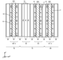
- FIG. 1 is a top view showing an example of a semiconductor device 100 according to one embodiment of the present invention
- FIG. 2 is an enlarged view of a region D in FIG. 1
- FIG. 3 is a diagram showing an example of an ee cross section in FIG. 2
- FIG. 10 is a diagram showing another example of the ee cross section
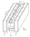
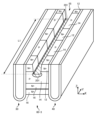
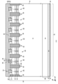
- 3 is a perspective cross-sectional view showing an example of a mesa portion 60 of a transistor portion 70
- FIG. FIG. 8 is a perspective cross-sectional view showing another example of the mesa portion 60-1 of the transistor portion 70
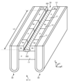
- 3 is a perspective cross-sectional view showing an example of a mesa portion 61 of a diode portion 80.
- FIG. 4 is a perspective cross-sectional view showing an example of a mesa portion 62 of a boundary portion 72;
- FIG. 3B shows an example of a YZ cross section along line aa shown in FIG. 3A.
- 3B shows another example of the YZ cross section taken along line aa shown in FIG. 3A.
- 3B shows an example of a YZ cross section taken along line bb shown in FIG. 3A.
- 3B shows an example of a YZ cross section along line cc shown in FIG. 3A.
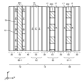
- An XZ cross section of the mesa portion 60 in the vicinity of the trench contact portion 55 is shown.
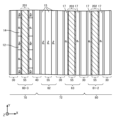
- Another example of the XZ cross section in the vicinity of the trench contact portion 55 of the mesa portion 60 is shown.
- FIG. 8 is a diagram showing another example of the mesa portion 60 of the transistor portion 70.
- FIG. It is a view showing a YZ cross section of the mesa portion 60-2.
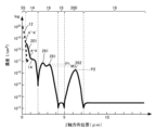
- FIG. 8 is a diagram showing an example of doping concentration distribution along the ff line of FIG. 7; It is a figure which shows the structural example of the trench contact part 55 in each mesa part. It is a figure which shows the structural example of the trench contact part 55 in each mesa part.
- 8 is a diagram showing another example of the mesa portion 60 of the transistor portion 70.
- FIG. FIG. 10 is a diagram showing another example of the mesa portion 60-3; 8 is a diagram showing another example of the mesa portion 61 of the diode portion 80.
- FIG. 8 is a diagram showing another example of the mesa portion 61 of the diode portion 80.
- FIG. FIG. 4 is a diagram showing an example of a combination of mesa portions in the semiconductor device 100; 4A and 4B are diagrams showing other examples of combinations of mesa portions in the semiconductor device 100; FIG. 4A and 4B are diagrams showing other examples of combinations of mesa portions in the semiconductor device 100; FIG. 4A and 4B are diagrams showing other examples of combinations of mesa portions in the semiconductor device 100; FIG. 4A and 4B are diagrams showing other examples of combinations of mesa portions in the semiconductor device 100; FIG. 4A and 4B are diagrams showing other examples of combinations of mesa portions in the semiconductor device 100; FIG. 4A and 4B are diagrams showing other examples of combinations of mesa portions in the semiconductor device 100; FIG.
- FIG. 3 is an ee cross section showing another configuration example of the semiconductor device 100.
- FIG. 3 is an ee cross section showing another configuration example of the semiconductor device 100.
- FIG. 3 is a top view showing another configuration example of the semiconductor device 100;
- FIG. 3 is a top view showing another configuration example of the semiconductor device 100;
- FIG. 3 is a top view showing another configuration example of the semiconductor device 100;
- FIG. 3 is a top view showing another configuration example of the semiconductor device 100;
- FIG. 3 is a top view showing another configuration example of the semiconductor device 100;
- FIG. 3 is a diagram showing another configuration example of the semiconductor device 100;
- FIG. 34 is a diagram showing an example of an ee cross section in FIG. 33; 3 is a diagram showing another configuration example of the semiconductor device 100;
- FIG. 35B is a diagram showing an example of the doping concentration distribution of the aa cross section and the a'-a' cross section in FIG. 35A;
- FIG. It shows an example in which a trench bottom region 260 is added to the structure of the mesa portion 60 shown in FIG. 7A. It shows an example in which a trench bottom region 260 is added to the structure of the mesa portion 61 shown in FIG. It shows an example in which a trench bottom region 260 is added to the structure of the mesa portion 62 shown in FIG. 3 is a diagram showing another configuration example of the semiconductor device 100;
- FIG. 35B is a diagram showing an example of the doping concentration distribution of the aa cross section and the a'-a' cross section in FIG. 35A;
- FIG. It shows an example in which a trench bottom region 260 is added to the structure
- one side in the direction parallel to the depth direction of the semiconductor substrate is called “upper”, and the other side is called “lower”.
- One of the two main surfaces of a substrate, layer or other member is called the upper surface and the other surface is called the lower surface.
- the directions of “up” and “down” are not limited to the direction of gravity or the direction when the semiconductor device is mounted.
- the Cartesian coordinate axes only specify the relative positions of the components and do not limit any particular orientation.
- the Z axis does not limit the height direction with respect to the ground.
- the +Z-axis direction and the ⁇ Z-axis direction are directions opposite to each other.
- the Z-axis direction is described without indicating positive or negative, it means a direction parallel to the +Z-axis and -Z-axis.
- orthogonal axes parallel to the upper and lower surfaces of the semiconductor substrate are defined as the X-axis and the Y-axis.
- the axis perpendicular to the upper and lower surfaces of the semiconductor substrate is defined as the Z-axis.
- the Z-axis direction may be referred to as the depth direction.
- a direction parallel to the upper and lower surfaces of the semiconductor substrate, including the X-axis and Y-axis may be referred to as a horizontal direction.
- the region from the center of the semiconductor substrate in the depth direction to the upper surface of the semiconductor substrate may be referred to as the upper surface side.
- the region from the center of the semiconductor substrate in the depth direction to the bottom surface of the semiconductor substrate may be referred to as the bottom surface side.
- the conductivity type of the doping region doped with impurities is described as P-type or N-type.
- impurities may specifically refer to either N-type donors or P-type acceptors, and may also be referred to as dopants.
- doping means introducing donors or acceptors into a semiconductor substrate to make it a semiconductor exhibiting N-type conductivity or a semiconductor exhibiting P-type conductivity.
- doping concentration means the concentration of donors or the concentration of acceptors at thermal equilibrium.
- the net doping concentration means the net concentration including charge polarity, where the donor concentration is the positive ion concentration and the acceptor concentration is the negative ion concentration.
- the donor concentration is N D and the acceptor concentration is N A , then the net net doping concentration at any location is N D ⁇ N A.
- net doping concentration may be simply referred to as doping concentration.
- a donor has the function of supplying electrons to a semiconductor.
- the acceptor has the function of receiving electrons from the semiconductor.
- Donors and acceptors are not limited to impurities per se.
- VOH defects in which vacancies (V), oxygen (O), and hydrogen (H) are combined in semiconductors function as donors that supply electrons.
- VOH defects are sometimes referred to herein as hydrogen donors.
- the semiconductor substrate herein is distributed throughout with N-type bulk donors.
- Bulk donors are donors from dopants that are substantially uniformly contained within the ingot during the manufacture of the ingot from which the semiconductor substrate is made.
- the bulk donor in this example is an element other than hydrogen.
- Bulk donor dopants include, but are not limited to, phosphorus, antimony, arsenic, selenium or sulfur.
- the bulk donor in this example is phosphorus.
- Bulk donors are also included in the P-type regions.
- the semiconductor substrate may be a wafer cut from a semiconductor ingot, or may be a chip obtained by singulating the wafer.
- Semiconductor ingots may be manufactured by any of the Czochralski method (CZ method), the magnetic field applied Czochralski method (MCZ method), and the float zone method (FZ method).
- the ingot in this example is manufactured by the MCZ method.
- the oxygen concentration contained in the substrate manufactured by the MCZ method is 1 ⁇ 10 17 to 7 ⁇ 10 17 /cm 3 .
- the oxygen concentration contained in the substrate manufactured by the FZ method is 1 ⁇ 10 15 to 5 ⁇ 10 16 /cm 3 .
- a higher oxygen concentration tends to generate hydrogen donors more easily.
- the bulk donor concentration may be the chemical concentration of bulk donors distributed throughout the semiconductor substrate and may be between 90% and 100% of the chemical concentration.
- a non-doped substrate that does not contain a dopant such as phosphorus may be used as the semiconductor substrate.
- the bulk donor concentration (D0) of the non-doped substrate is, for example, 1 ⁇ 10 10 /cm 3 or more and 5 ⁇ 10 12 /cm 3 or less.
- the bulk donor concentration (D0) of the non-doped substrate is preferably 1 ⁇ 10 11 /cm 3 or higher.
- the bulk donor concentration (D0) of the non-doped substrate is preferably 5 ⁇ 10 12 /cm 3 or less.
- Each concentration in the present invention may be a value at room temperature. As an example of the value at room temperature, the value at 300 K (Kelvin) (approximately 26.9° C.) may be used.
- references herein to P-type or N-type refer to higher doping concentrations than P-type or N-type; references to P-type or N-type refer to higher doping than P-type or N-type. It means that the concentration is low.
- P++ type or N++ type in this specification means that the doping concentration is higher than that of the P+ type or N+ type.
- the unit system in this specification is the SI unit system unless otherwise specified. The unit of length is sometimes displayed in cm, but various calculations may be performed after converting to meters (m).
- chemical concentration refers to the atomic density of impurities measured regardless of the state of electrical activation. Chemical concentrations can be measured, for example, by secondary ion mass spectroscopy (SIMS).
- the net doping concentrations mentioned above can be measured by the voltage-capacitance method (CV method).
- the carrier concentration measured by the spreading resistance measurement method (SR method) may be used as the net doping concentration.
- the carrier concentration measured by the CV method or SR method may be a value in thermal equilibrium.
- the donor concentration is sufficiently higher than the acceptor concentration in the N-type region, the carrier concentration in the region may be used as the donor concentration.
- the carrier concentration in that region may be used as the acceptor concentration.
- the doping concentration of the N-type regions is sometimes referred to herein as the donor concentration
- the doping concentration of the P-type regions is sometimes referred to as the acceptor concentration.
- the peak value may be taken as the concentration of donors, acceptors or net doping in the region.
- the average value of the concentration of donors, acceptors or net doping in the region may be used as the concentration of donors, acceptors or net doping.
- atoms/cm 3 or /cm 3 are used to express concentration per unit volume. This unit is used for donor or acceptor concentrations, or chemical concentrations, within a semiconductor substrate. The atoms notation may be omitted.
- the carrier concentration measured by the SR method may be lower than the donor or acceptor concentration.
- the carrier mobility of the semiconductor substrate may be lower than the value in the crystalline state. A decrease in carrier mobility is caused by scattering of carriers due to disorder of the crystal structure due to lattice defects or the like.
- the donor or acceptor concentration calculated from the carrier concentration measured by the CV method or the SR method may be lower than the chemical concentration of the element representing the donor or acceptor.
- the donor concentration of phosphorus or arsenic as a donor or the acceptor concentration of boron (boron) as an acceptor in a silicon semiconductor is about 99% of these chemical concentrations.
- the donor concentration of hydrogen serving as a donor in a silicon semiconductor is about 0.1% to 10% of the chemical concentration of hydrogen.
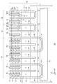
- FIG. 1 is a top view showing an example of a semiconductor device 100 according to one embodiment of the present invention.
- FIG. 1 shows the positions of each member projected onto the upper surface of the semiconductor substrate 10 .
- FIG. 1 only some members of the semiconductor device 100 are shown, and some members are omitted.
- a semiconductor device 100 includes a semiconductor substrate 10 .
- the semiconductor substrate 10 is a substrate made of a semiconductor material.
- the semiconductor substrate 10 is a silicon substrate.
- the semiconductor substrate 10 has an edge 162 when viewed from above. In this specification, simply referring to a top view means viewing from the top side of the semiconductor substrate 10 .
- the semiconductor substrate 10 of this example has two sets of edges 162 facing each other when viewed from above. In FIG. 1 , the X-axis and Y-axis are parallel to one of the edges 162 . Also, the Z-axis is perpendicular to the upper surface of the semiconductor substrate 10 .
- An active portion 160 is provided on the semiconductor substrate 10 .
- the active portion 160 is a region through which a main current flows in the depth direction between the upper and lower surfaces of the semiconductor substrate 10 when the semiconductor device 100 operates.
- An emitter electrode is provided above the active portion 160, but is omitted in FIG.
- the active portion 160 may refer to a region overlapping the emitter electrode when viewed from above. Also, the active portion 160 may include a region sandwiched between the active portions 160 when viewed from above.
- the active section 160 is provided with a transistor section 70 including transistor elements such as IGBTs.
- the active portion 160 may further include a diode portion 80 including a diode element such as a freewheeling diode (FWD).
- FWD freewheeling diode
- the transistor portions 70 and the diode portions 80 are alternately arranged along a predetermined arrangement direction (X-axis direction in this example) on the upper surface of the semiconductor substrate 10 .
- the semiconductor device 100 of this example is a reverse conducting IGBT (RC-IGBT).
- the region where the transistor section 70 is arranged is denoted by the symbol "I”
- the region where the diode section 80 is arranged is denoted by the symbol "F”.
- the direction perpendicular to the arrangement direction in top view may be referred to as the stretching direction (the Y-axis direction in FIG. 1).
- the transistor section 70 and the diode section 80 may each have a length in the extending direction. That is, the length in the Y-axis direction of the transistor section 70 is greater than the width in the X-axis direction. Similarly, the length in the Y-axis direction of the diode section 80 is greater than the width in the X-axis direction.
- the extending direction of the transistor portion 70 and the diode portion 80 may be the same as the longitudinal direction of each trench portion.
- the diode section 80 has an N+ type cathode region in a region in contact with the lower surface of the semiconductor substrate 10 .
- the region provided with the cathode region is referred to as the diode section 80 . That is, the diode portion 80 is a region that overlaps with the cathode region when viewed from above.
- a P + -type collector region may be provided in a region other than the cathode region on the lower surface of the semiconductor substrate 10 .
- the diode section 80 may also include an extension region 81 extending in the Y-axis direction from the diode section 80 to the gate wiring described later.
- a collector region is provided on the lower surface of the extension region 81 .
- the transistor section 70 has a P+ type collector region in a region in contact with the lower surface of the semiconductor substrate 10 .
- a gate structure having an N-type emitter region, a P-type base region, a gate conductive portion, and a gate insulating film is periodically arranged on the upper surface side of the semiconductor substrate 10 .
- the semiconductor device 100 may have one or more pads above the semiconductor substrate 10 .
- the semiconductor device 100 of this example has a gate pad 164 .
- Semiconductor device 100 may have pads such as an anode pad, a cathode pad, and a current sensing pad. Each pad is arranged near the edge 162 .
- the vicinity of the edge 162 refers to a region between the edge 162 and the emitter electrode in top view.
- each pad may be connected to an external circuit via a wiring such as a wire.
- a gate potential is applied to the gate pad 164 .
- Gate pad 164 is electrically connected to the conductive portion of the gate trench portion of active portion 160 .
- the semiconductor device 100 includes a gate wiring that connects the gate pad 164 and the gate trench portion. In FIG. 1, the gate wiring is hatched with oblique lines.
- the gate wiring of this example has a peripheral gate wiring 130 and an active side gate wiring 131 .
- the peripheral gate wiring 130 is arranged between the active portion 160 and the edge 162 of the semiconductor substrate 10 when viewed from above.
- the peripheral gate wiring 130 of this example surrounds the active portion 160 when viewed from above.
- a region surrounded by the peripheral gate wiring 130 in a top view may be the active portion 160 .
- a well region is formed below the gate wiring.
- a well region is a P-type region having a higher concentration than a base region, which will be described later, and is formed from the upper surface of the semiconductor substrate 10 to a position deeper than the base region.
- a region surrounded by the well region in top view may be the active portion 160 .
- the peripheral gate wiring 130 is connected to the gate pad 164 .
- the peripheral gate wiring 130 is arranged above the semiconductor substrate 10 .
- the peripheral gate wiring 130 may be a metal wiring containing aluminum or the like.
- the active side gate wiring 131 is provided in the active portion 160 .
- variations in wiring length from the gate pad 164 can be reduced for each region of the semiconductor substrate 10 .
- the peripheral gate wiring 130 and the active side gate wiring 131 are connected to the gate trench portion of the active portion 160 .
- the peripheral gate wiring 130 and the active side gate wiring 131 are arranged above the semiconductor substrate 10 .
- the peripheral gate wiring 130 and the active side gate wiring 131 may be wirings formed of a semiconductor such as polysilicon doped with impurities.
- the active side gate wiring 131 may be connected to the peripheral gate wiring 130 .
- the active-side gate wiring 131 of this example extends in the X-axis direction from one outer peripheral gate wiring 130 sandwiching the active portion 160 to the other outer peripheral gate wiring 130 so as to cross the active portion 160 at substantially the center in the Y-axis direction. is provided.
- the transistor portions 70 and the diode portions 80 may be alternately arranged in the X-axis direction in each divided region.
- the semiconductor device 100 also includes a temperature sensing portion (not shown), which is a PN junction diode made of polysilicon or the like, and a current detecting portion (not shown) that simulates the operation of the transistor portion provided in the active portion 160. good too.
- a temperature sensing portion which is a PN junction diode made of polysilicon or the like
- a current detecting portion (not shown) that simulates the operation of the transistor portion provided in the active portion 160. good too.
- the semiconductor device 100 of this example includes an edge termination structure portion 90 between the active portion 160 and the edge 162 when viewed from above.
- the edge termination structure 90 in this example is located between the peripheral gate line 130 and the edge 162 .
- the edge termination structure 90 reduces electric field concentration on the upper surface side of the semiconductor substrate 10 .
- Edge termination structure 90 may include at least one of a guard ring, a field plate, and a resurf annularly surrounding active portion 160 .
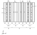
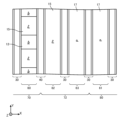
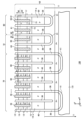
- FIG. 2 is an enlarged view of area D in FIG.
- Region D is a region including transistor section 70 , diode section 80 , and active-side gate wiring 131 .
- a boundary portion 72 may be provided between the transistor portion 70 and the diode portion 80 .
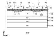
- the semiconductor device 100 of this example includes a gate trench portion 40 , a dummy trench portion 30 , a well region 11 , an emitter region 12 , a base region 14 and a contact region 15 provided inside the upper surface side of the semiconductor substrate 10 .
- Each of the gate trench portion 40 and the dummy trench portion 30 is an example of the trench portion.
- the semiconductor device 100 of this example also includes an emitter electrode 52 and an active-side gate wiring 131 provided above the upper surface of the semiconductor substrate 10 . Emitter electrode 52 and active-side gate line 131 are provided separately from each other.
- An interlayer insulating film is provided between the emitter electrode 52 and the active-side gate wiring 131 and the upper surface of the semiconductor substrate 10, but is omitted in FIG.
- a contact hole is provided through the interlayer insulating film of this example.
- a conductive member such as the emitter electrode 52 may be provided inside the contact hole.
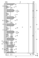
- a trench contact portion 55 is provided on the upper surface of the semiconductor substrate 10 of this example.
- the trench contact portion 55 is a member in which a groove-like structure provided to a predetermined depth from the upper surface of the semiconductor substrate 10 is filled with a conductive material.
- the inside of the trench of the trench contact portion 55 is filled with a conductive material such as tungsten.
- a barrier metal containing at least one of a titanium film and a titanium nitride film may be provided between the conductive member and the semiconductor substrate 10 inside the trench of the trench contact portion 55 .
- the trench contact portion 55 is provided extending in the extension direction (Y-axis direction).
- the trench contact portion 55 is arranged below the contact hole of the interlayer insulating film described above.
- Emitter electrode 52 may be connected to semiconductor substrate 10 via a contact hole in the interlayer insulating film and trench contact portion 55 . In FIG. 2, each trench contact portion 55 is hatched with oblique lines.
- the emitter electrode 52 is provided above the gate trench portion 40 , the dummy trench portion 30 , the well region 11 , the emitter region 12 , the base region 14 and the contact region 15 .
- Emitter electrode 52 contacts at least part of well region 11 , emitter region 12 , contact region 15 , anode region 17 and base region 14 on the upper surface of semiconductor substrate 10 through contact hole and trench contact portion 55 .
- the emitter electrode 52 is connected to the dummy conductive portion in the dummy trench portion 30 through a contact hole provided in the interlayer insulating film.
- the emitter electrode 52 may be connected to the dummy conductive portion of the dummy trench portion 30 at the tip of the dummy trench portion 30 in the Y-axis direction.
- the active-side gate wiring 131 is connected to the gate trench portion 40 through a contact hole provided in the interlayer insulating film.
- the active-side gate wiring 131 may be connected to the gate conductive portion of the gate trench portion 40 at the tip portion 41 of the gate trench portion 40 in the Y-axis direction.
- the active-side gate wiring 131 is not connected to the dummy conductive portion within the dummy trench portion 30 .
- the emitter electrode 52 is made of a material containing metal.
- FIG. 2 shows the range in which the emitter electrode 52 is provided.
- the emitter electrode 52 is made of aluminum or a metal alloy such as an aluminum-silicon alloy such as AlSi, AlSiCu.
- the emitter electrode 52 may have a barrier metal made of titanium, a titanium compound, or the like under the region made of aluminum or the like. Further, the contact hole may have a plug formed by embedding tungsten or the like so as to be in contact with the barrier metal and the aluminum or the like.
- the well region 11 is provided so as to overlap with the active side gate wiring 131 .
- the well region 11 is also provided extending with a predetermined width in a range not overlapping the active side gate wiring 131 .
- the well region 11 of this example is provided away from the Y-axis direction end of the contact hole on the active side gate wiring 131 side.
- the well region 11 is a second conductivity type region having a higher doping concentration than the base region 14 .
- the base region 14 in this example is of P type and the well region 11 is of P+ type.
- Each of the transistor section 70, the boundary section 72 and the diode section 80 has one or more trench sections arranged in the arrangement direction.
- one or more gate trench sections 40 and one or more dummy trench sections 30 are alternately provided along the arrangement direction.
- a plurality of dummy trench portions 30 are provided along the array direction in the diode portion 80 of this example.
- the gate trench portion 40 is not provided in the diode portion 80 of this example.
- One or more dummy trench portions 30 are provided in the boundary portion 72 of this example along the arrangement direction.
- a gate trench portion 40 may be further provided in the boundary portion 72 .
- the gate trench portion 40 of this example connects the two straight portions 39 extending along the extending direction perpendicular to the arrangement direction (the portion of the trench that is linear along the extending direction) and the two straight portions 39 . It may have a tip 41 .
- the stretching direction in FIG. 2 is the Y-axis direction.
- At least a portion of the tip portion 41 is preferably provided in a curved shape when viewed from above.
- the dummy trench portions 30 are provided between the respective straight portions 39 of the gate trench portions 40 .
- One dummy trench portion 30 may be provided between the straight portions 39, or a plurality of dummy trench portions 30 may be provided.
- the dummy trench portion 30 may have a linear shape extending in the extending direction, and may have a linear portion 29 and a tip portion 31 like the gate trench portion 40 .
- the semiconductor device 100 shown in FIG. 2 includes both linear dummy trench portions 30 without tip portions 31 and dummy trench portions 30 with tip portions 31 .
- the diffusion depth of the well region 11 may be deeper than the depths of the gate trench portion 40 and the dummy trench portion 30 .
- Y-axis direction ends of the gate trench portion 40 and the dummy trench portion 30 are provided in the well region 11 when viewed from above. That is, the bottom of each trench in the depth direction is covered with the well region 11 at the end of each trench in the Y-axis direction. As a result, electric field concentration at the bottom of each trench can be relaxed.
- a mesa portion is provided between each trench portion in the arrangement direction.
- the mesa portion refers to a region sandwiched between trench portions inside the semiconductor substrate 10 .
- the upper end of the mesa portion is the upper surface of the semiconductor substrate 10 .
- the depth position of the lower end of the mesa portion is the same as the depth position of the lower end of the trench portion.
- the mesa portion of this example extends in the extension direction (Y-axis direction) along the trench on the upper surface of the semiconductor substrate 10 .
- the transistor portion 70 is provided with a mesa portion 60
- the diode portion 80 is provided with a mesa portion 61
- the boundary portion 72 is provided with a mesa portion 62 and a mesa portion 63 .
- the mesa portion 62 is the mesa portion closest to the transistor portion 70 at the boundary portion 72
- the mesa portion 63 is the mesa portion closest to the diode portion 80 at the boundary portion 72 .
- One or more mesas 62 may be further provided between the mesas 62 and 63
- One or more mesas 63 may be further provided between the mesas 62 and 63 .
- a mesa portion it refers to the mesa portion 60, the mesa portion 61, the mesa portion 62, and the mesa portion 63, respectively.
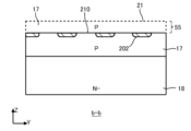
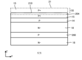
- a base region 14 is provided in each mesa portion. Of the base regions 14 exposed on the upper surface of the semiconductor substrate 10 in the mesa portion, the region arranged closest to the active-side gate wiring 131 is referred to as a base region 14-e. Although FIG. 2 shows the base region 14-e arranged at one end in the extending direction of each mesa, the base region 14-e is also arranged at the other end of each mesa. It is Each mesa portion has at least one of the first conductive type emitter region 12, the second conductive type contact region 15 and the second conductive type anode region 17 in the region sandwiched between the base regions 14-e when viewed from above. Either may be provided.
- the emitter region 12 in this example is of N+ type, the contact region 15 is of P+ type, and the anode region 17 is of P type.
- Emitter region 12 and contact region 15 may be provided between base region 14 and the upper surface of semiconductor substrate 10 in the depth direction.
- Anode region 17 may be provided at the same depth range as base region 14 .
- Anode region 17 may have the same doping concentration as base region 14 or may have a lower doping concentration than base region 14 .
- the mesa portion 60 of the transistor portion 70 has the emitter region 12 exposed on the upper surface of the semiconductor substrate 10 .
- the emitter region 12 is provided in contact with the gate trench portion 40 .
- the mesa portion 60 in contact with the gate trench portion 40 may be provided with the contact region 15 exposed to the upper surface of the semiconductor substrate 10 .
- Each of the contact region 15 and the emitter region 12 in the mesa portion 60 is provided from one trench portion to the other trench portion in the X-axis direction.
- the contact regions 15 and the emitter regions 12 of the mesa portion 60 are alternately arranged along the extension direction (Y-axis direction) of the trench portion.
- the contact regions 15 and the emitter regions 12 of the mesa portion 60 may be provided in stripes along the extending direction (Y-axis direction) of the trench portion.
- an emitter region 12 is provided in a region in contact with the trench portion, and a contact region 15 is provided in a region sandwiched between the emitter regions 12 .
- the mesa portion 61 of the diode portion 80 is not provided with the emitter region 12 .
- a base region 14 , an anode region 17 and a contact region 15 may be provided on the upper surface of the mesa portion 61 .
- a contact region 15 may be provided in a region sandwiched between the base regions 14-e on the upper surface of the mesa portion 61 so as to be in contact with each base region 14-e.
- An anode region 17 may be provided in a region sandwiched between the contact regions 15 on the upper surface of the mesa portion 61 .
- the anode region 17 may be arranged over the entire region sandwiched between the contact regions 15 .
- a contact region 15 may be provided on the upper surface of the mesa portion 62 of the boundary portion 72 .
- the contact region 15 is the entire region sandwiched between the base regions 14 - e on the upper surface of the mesa portion 61 .
- the emitter region 12 is not provided in the mesa portion 63 of the boundary portion 72 .
- a base region 14 , an anode region 17 and a contact region 15 may be provided on the upper surface of the mesa portion 63 .
- a contact region 15 may be provided in a region sandwiched between the base regions 14-e on the upper surface of the mesa portion 63 so as to be in contact with each base region 14-e.
- An anode region 17 may be provided in a region sandwiched between the contact regions 15 on the upper surface of the mesa portion 63 .
- the anode region 17 may be arranged over the entire region sandwiched between the contact regions 15 .
- the structures of the mesa portion 61 and the mesa portion 63 are the same.
- mesa portion 63 may have a different structure than mesa portion 61 .
- a trench contact portion 55 is provided in each mesa portion.
- a contact hole is provided in the interlayer insulating film above the trench contact portion 55 .
- the trench contact portion 55 is arranged in a region sandwiched between the base regions 14-e.
- the trench contact portion 55 of this example is provided above each region of the contact region 15 , the base region 14 , the anode region 17 and the emitter region 12 .
- Trench contact portion 55 is not provided in a region corresponding to base region 14 - e and well region 11 .
- the trench contact portion 55 may be arranged at the center in the arrangement direction (X-axis direction) of each mesa portion.
- an N+ type cathode region 82 is provided in a region in contact with the lower surface of the semiconductor substrate 10 .
- a P + -type collector region 22 may be provided in a region of the lower surface of the semiconductor substrate 10 where the cathode region 82 is not provided.
- a collector region 22 is provided in a region in contact with the lower surface of semiconductor substrate 10 in transistor portion 70 and boundary portion 72 . In FIG. 2, the boundary between cathode region 82 and collector region 22 is indicated by a dotted line.
- the cathode region 82 is arranged apart from the well region 11 in the Y-axis direction. As a result, the distance between the P-type region (well region 11), which has a relatively high doping concentration and is formed to a deep position, and the cathode region 82 can be secured, and the withstand voltage can be improved.
- the ends of the cathode regions 82 in the Y-axis direction in this example are arranged farther from the well region 11 than the ends of the trench contact portions 55 in the Y-axis direction.
- the end of the cathode region 82 in the Y-axis direction may be arranged between the well region 11 and the trench contact portion 55 .
- FIG. 3A is a diagram showing an example of the ee cross section in FIG.
- the ee section is the XZ plane passing through emitter region 12 and cathode region 82 .
- the semiconductor device 100 of this example has a semiconductor substrate 10, an interlayer insulating film 38, an emitter electrode 52 and a collector electrode 24 in the cross section.
- the interlayer insulating film 38 is provided on the upper surface of the semiconductor substrate 10 .
- the interlayer insulating film 38 is a film including at least one layer of an insulating film such as silicate glass doped with an impurity such as boron or phosphorus, a thermal oxide film, and other insulating films.
- the contact hole 54 described with reference to FIG. 2 is provided in the interlayer insulating film 38 .
- the emitter electrode 52 is provided above the interlayer insulating film 38 .
- Emitter electrode 52 is connected to semiconductor substrate 10 through contact hole 54 in interlayer insulating film 38 .
- the contact hole 54 may be filled with the same conductive material as the emitter electrode 52 above the interlayer insulating film 38, or may be filled with a different conductive material.
- a collector electrode 24 is provided on the lower surface 23 of the semiconductor substrate 10 .
- Emitter electrode 52 and collector electrode 24 are made of a metal material such as aluminum.
- the inside of the contact hole 54 may be filled with tungsten or the like.
- the direction (Z-axis direction) connecting the emitter electrode 52 and the collector electrode 24 is referred to as the depth direction.
- the semiconductor substrate 10 has an N-type or N ⁇ type drift region 18 .
- Drift region 18 is provided in each of transistor section 70 , boundary section 72 and diode section 80 .
- an N+ type emitter region 12 and a P type base region 14 are provided in order from the upper surface 21 side of the semiconductor substrate 10 .
- a drift region 18 is provided below the base region 14 .
- the mesa portion 60 may be provided with an N+ type accumulation region 16 .
- Accumulation region 16 is disposed between base region 14 and drift region 18 .
- the emitter region 12 is exposed on the upper surface 21 of the semiconductor substrate 10 and provided in contact with the gate trench portion 40 .
- the emitter region 12 may be in contact with trench portions on both sides of the mesa portion 60 .
- Emitter region 12 has a higher doping concentration than drift region 18 .
- the base region 14 is provided below the emitter region 12 .
- the base region 14 in this example is provided in contact with the emitter region 12 .
- the base region 14 may contact trench portions on both sides of the mesa portion 60 .
- the accumulation region 16 is provided below the base region 14 .
- the accumulation region 16 is an N+ type region with a higher doping concentration than the drift region 18 . That is, the accumulation region 16 has a higher donor concentration than the drift region 18 .
- the carrier injection promoting effect IE effect
- the accumulation region 16 may be provided so as to cover the entire bottom surface of the base region 14 in each mesa portion 60 .
- the mesa portion 60 may be provided with two or more accumulation regions 16 in the depth direction. Each accumulation region 16 has a doping concentration peak in the depth direction. Between the two accumulation regions 16 there is a trough of doping concentration in the depth direction. That is, mesa portion 60 may have more than one doping concentration peak from base region 14 toward drift region 18 .
- a drift region 18 may be provided between the accumulation region 16 and the base region 14, and the accumulation region 16 and the base region 14 may be in contact.
- the boundary portion 72 and the diode portion 80 may or may not be provided with the accumulation region 16 . In this example, neither the boundary portion 72 nor the diode portion 80 is provided with the accumulation region 16 .
- a P-type anode region 17 is provided in the mesa portion 61 of the diode portion 80 in contact with the upper surface 21 of the semiconductor substrate 10 .
- a drift region 18 is provided below the anode region 17 .
- the anode region 17 may have the same doping concentration as the base region 14 or may have a lower doping concentration than the base region 14. . By reducing the concentration of the anode region 17, it is possible to suppress hole injection in the mesa portion 61 and reduce the reverse recovery loss.
- a P+ type contact region 15 is provided in the mesa portion 62 of the boundary portion 72 so as to be in contact with the upper surface 21 of the semiconductor substrate 10 .
- Base region 14 or anode region 17 may be provided between contact region 15 and drift region 18 , and contact region 15 and drift region 18 may be in contact.
- a P-type anode region 17 is provided in the mesa portion 63 of the boundary portion 72 so as to be in contact with the upper surface 21 of the semiconductor substrate 10 .
- a drift region 18 is provided below the anode region 17 .
- An N+ type buffer region 20 may be provided under the drift region 18 in each of the transistor section 70 , the boundary section 72 and the diode section 80 .
- the doping concentration of buffer region 20 is higher than the doping concentration of drift region 18 .
- Buffer region 20 may have a concentration peak with a higher doping concentration than drift region 18 .
- the doping concentration of the concentration peak refers to the doping concentration at the apex of the concentration peak.
- an average value of doping concentrations in a region where the doping concentration distribution is substantially flat may be used as the doping concentration of the drift region 18.
- the buffer region 20 may have two or more concentration peaks in the depth direction (Z-axis direction) of the semiconductor substrate 10 .
- the concentration peak of the buffer region 20 may be provided at the same depth position as the chemical concentration peak of hydrogen (protons) or phosphorus, for example.
- Buffer region 20 may function as a field stop layer that prevents a depletion layer extending from the bottom edge of base region 14 from reaching P + -type collector region 22 and N + -type cathode region 82 .
- a P+ type collector region 22 is provided below the buffer region 20 in the transistor portion 70 and the boundary portion 72 .
- the doping concentration of collector region 22 is higher than the doping concentration of base region 14 .
- Collector region 22 may contain the same acceptor as base region 14 or may contain a different acceptor.
- the acceptor of the collector region 22 is boron, for example.
- An N+ type cathode region 82 is provided under the buffer region 20 in the diode section 80 .
- the doping concentration of cathode region 82 is higher than the doping concentration of drift region 18 .
- the donor for cathode region 82 is, for example, hydrogen or phosphorus. Note that the elements that serve as donors and acceptors in each region are not limited to the above examples.
- Collector region 22 and cathode region 82 are exposed at lower surface 23 of semiconductor substrate 10 and connected to collector electrode 24 .
- Collector electrode 24 may contact the entire bottom surface 23 of semiconductor substrate 10 .
- Emitter electrode 52 and collector electrode 24 are made of a metal material such as aluminum.
- part of the cathode region 82 may be replaced with a P-type region.
- the P-type region is sandwiched between cathode regions 82 .
- the P-type region may be sandwiched between the cathode regions 82 in the Y-axis direction.
- One or more gate trench portions 40 and one or more dummy trench portions 30 are provided on the upper surface 21 side of the semiconductor substrate 10 .
- Each trench portion extends from the upper surface 21 of the semiconductor substrate 10 through the base region 14 to below the base region 14 .
- the contact region 15 and/or the storage region 16 are provided, each trench section also passes through these doping regions.
- the fact that the trench penetrates the doping region is not limited to the order of forming the doping region and then forming the trench.
- a structure in which a doping region is formed between the trench portions after the trench portions are formed is also included in the structure in which the trench portion penetrates the doping regions.
- the transistor section 70 is provided with the gate trench section 40 and the dummy trench section 30 .
- a dummy trench portion 30 is provided in the boundary portion 72 .
- a gate trench portion 40 may be further provided in the boundary portion 72 .
- the diode section 80 is provided with the dummy trench section 30 and is not provided with the gate trench section 40 .
- the boundary between the collector region 22 and the cathode region 82 may be the boundary between the boundary portion 72 and the diode portion 80 in the X-axis direction. If the boundary portion 72 is not provided, the boundary between the collector region 22 and the cathode region 82 may be used as the boundary between the transistor portion 70 and the diode portion 80 in the X-axis direction. Further, among the trench portions in contact with the emitter region 12 , the trench portion closest to the diode portion 80 may be used as the boundary between the transistor portion 70 and the boundary portion 72 .
- the gate trench portion 40 has a gate trench provided in the upper surface 21 of the semiconductor substrate 10, a gate insulating film 42 and a gate conductive portion 44.
- a gate insulating film 42 is provided to cover the inner wall of the gate trench.
- the gate insulating film 42 may be formed by oxidizing or nitriding the semiconductor on the inner wall of the gate trench.
- the gate conductive portion 44 is provided inside the gate insulating film 42 inside the gate trench. That is, the gate insulating film 42 insulates the gate conductive portion 44 and the semiconductor substrate 10 from each other.
- the gate conductive portion 44 is formed of a conductive material such as polysilicon.
- the gate conductive portion 44 may be provided longer than the base region 14 in the depth direction.
- the gate trench portion 40 in the cross section is covered with the interlayer insulating film 38 on the upper surface 21 of the semiconductor substrate 10 .
- the gate conductive portion 44 is electrically connected to the gate wiring. When a predetermined gate voltage is applied to the gate conductive portion 44 , a channel is formed by an electron inversion layer in the surface layer of the interface contacting the gate trench portion 40 in the base region 14 .
- the dummy trench portion 30 may have the same structure as the gate trench portion 40 in the cross section.
- the dummy trench section 30 has a dummy trench provided in the upper surface 21 of the semiconductor substrate 10 , a dummy insulating film 32 and a dummy conductive section 34 .
- the dummy conductive portion 34 is electrically connected to the emitter electrode 52 .
- a dummy insulating film 32 is provided to cover the inner wall of the dummy trench.
- the dummy conductive portion 34 is provided inside the dummy trench and inside the dummy insulating film 32 .
- the dummy insulating film 32 insulates the dummy conductive portion 34 from the semiconductor substrate 10 .
- the dummy conductive portion 34 may be made of the same material as the gate conductive portion 44 .
- the dummy conductive portion 34 is made of a conductive material such as polysilicon.
- the dummy conductive portion 34 may have the same length as the gate conductive portion 44 in the depth direction.
- the gate trench portion 40 and the dummy trench portion 30 of this example are covered with an interlayer insulating film 38 on the upper surface 21 of the semiconductor substrate 10 .
- the bottoms of the dummy trench portion 30 and the gate trench portion 40 may be curved (curved in cross section) convex downward.
- At least one mesa portion 60 of the transistor portion 70 is provided with a trench contact portion 55 and a first bottom region 201 of the second conductivity type. All mesas 60 may be provided with trench contacts 55 and first bottom regions 201 .
- trench contact portion 55 is provided in the depth direction from upper surface 21 toward lower surface 23 of semiconductor substrate 10 .
- the trench contact portion 55 of this example is formed shallower than the lower end of the emitter region 12 .
- the trench contact portion 55 may be provided to the same depth as the bottom end of the emitter region 12 or may be formed deeper than the bottom end of the emitter region 12 .
- a plug 56 made of metal such as tungsten may be embedded in the trench contact portion 55 .
- the top surface 58 of the plug 56 may be the top surface 58 of the trench contact portion 55 .
- the top surface 58 of the plug 56 may be located on the emitter electrode 52 side (that is, above) the top surface 21 of the semiconductor substrate 10 .
- the trench contact portion 55 may be provided from the top surface 58 of the plug 56 to the bottom surface 23 side of the top surface 21 of the semiconductor substrate 10 .
- the upper surface 58 of the trench contact portion 55 may be positioned closer to the upper surface 21 than the upper surface of the interlayer insulating film 38 and may be positioned closer to the emitter electrode 52 than the upper surface 21 .
- the upper surface 58 of the trench contact portion 55 may be provided to the same depth position as the upper surface of the interlayer insulating film 38 .
- the first bottom region 201 in this example is a P+ type region with a higher doping concentration than the base region 14 .
- the first bottom region 201 is provided in contact with the bottom of the trench contact portion 55 .
- the first bottom region 201 connects with the base region 14 .
- At least part of the first bottom region 201 is provided below the emitter region 12 .
- the first bottom region 201 extends in the Y-axis direction along the trench contact portion 55 .
- the first bottom region 201 connects with the contact region 15 shown in FIG. According to this example, when the transistor portion 70 is turned off, holes directed from the lower surface 23 side toward the emitter region 12 can flow to the contact region 15 or the trench contact portion 55 through the first bottom region 201 . As a result, the resistance of the path through which holes pass can be reduced, and latch-up can be suppressed.
- At least one mesa portion 61 of the diode portion 80 is provided with a trench contact portion 55 and a second conductivity type second bottom region 202 . All mesas 61 may be provided with trench contacts 55 and second bottom regions 202 .
- the trench contact portion 55 of the diode portion 80 may have the same structure as the trench contact portion 55 of the transistor portion 70 .
- a lower end of the trench contact portion 55 of the diode portion 80 may be arranged inside the anode region 17 .
- the second bottom region 202 in this example is a P+ type region with a higher doping concentration than the anode region 17 and the base region 14 .
- the second bottom region 202 is provided in contact with the bottom of the trench contact portion 55 .
- a second bottom region 202 may be provided within the anode region 17 . That is, the second bottom region 202 does not have to contact the drift region 18 .
- the second bottom region 202 is provided extending in the Y-axis direction along the trench contact portion 55 .
- the length of the first bottom region 201 in the Y-axis direction is greater than the length of the second bottom region 202 in the Y-axis direction.
- a trench contact portion 55 is provided in the mesa portion 62 of the boundary portion 72 .
- the mesa portion 62 of the boundary portion 72 may be provided closest to the transistor portion 70 in the boundary portion 72 .
- the trench contact portion 55 of the mesa portion 62 may have the same structure as the trench contact portion 55 of the transistor portion 70 .
- a lower end of the trench contact portion 55 of the mesa portion 62 is arranged inside the contact region 15 .
- the lower end of trench contact portion 55 of mesa portion 62 is not provided with a P-type bottom region having a higher doping concentration than contact region 15 .
- a P-type bottom region 204 having a higher doping concentration than the contact region 15 may be provided at the lower end of the trench contact portion 55 of the mesa portion 62 .
- the dotted line indicates the position where the bottom region 204 is provided.
- the doping concentration of the contact region 15 the doping concentration of the upper surface 21 of the mesa portion 62 may be used.
- the mesa portion 63 of the boundary portion 72 is provided with the trench contact portion 55 and the third bottom region 203 of the second conductivity type.
- the mesa portion 63 of the boundary portion 72 may be provided closer to the diode portion 80 than the mesa portion 62 of the boundary portion 72 .
- All mesas 63 may be provided with trench contacts 55 and third bottom regions 203 .
- the trench contact portion 55 of the mesa portion 63 may have the same structure as the trench contact portion 55 of the transistor portion 70 .
- a lower end of the trench contact portion 55 of the mesa portion 63 may be arranged inside the anode region 17 .
- the third bottom region 203 in this example is a P+ type region with a higher doping concentration than the anode region 17 and the base region 14 .
- the third bottom region 203 is provided in contact with the bottom of the trench contact portion 55 .
- a third bottom region 203 may be provided inside the anode region 17 . That is, the third bottom region 203 does not have to be in contact with the drift region 18 .
- the third bottom region 203 is provided extending in the Y-axis direction along the trench contact portion 55 .
- the length of the first bottom region 201 in the Y-axis direction is greater than the length of the third bottom region 203 in the Y-axis direction.
- the third bottom region 203 By making the third bottom region 203 small, the injection amount of holes from the upper surface 21 side in the mesa portion 63 arranged near the diode portion 80 can be reduced. Therefore, the reverse recovery time of the diode section 80 can be shortened, and the reverse recovery loss can be reduced.
- the doping concentration, region size, shape and position on the Y-axis of the third bottom region 203 may be the same as the second bottom region 202 .
- the boundary portion 72 has one mesa portion 62 and one mesa portion 63 .
- boundary 72 may have multiple mesas 63 between mesas 62 and diodes 80 .
- the boundary portion 72 may have a plurality of mesa portions 62 between the mesa portion 63 and the transistor portion 70 .
- FIG. 3B is a diagram showing another example of the ee cross section.
- the trench contact portion 55 is formed deeper than in the example of FIG. 3A.
- Other structures may be similar to the semiconductor device 100 shown in FIG. 3A.
- the trench contact portion 55 is formed deeper than the emitter region 12 . That is, the trench contact portion 55 penetrates the emitter region 12 and the lower end of the trench contact portion 55 is arranged below the lower end of the emitter region 12 .
- a lower end of the trench contact portion 55 of the mesa portion 60 may be arranged at the same depth as the base region 14 .
- the trench contact portion 55 of another mesa portion may also have the same structure as the mesa portion 60 .
- the lower end of the trench contact portion 55 of the mesa portion 61 may be arranged at the same depth as the anode region 17 .
- the lower end of the trench contact portion 55 of the mesa portion 62 may be arranged at the same depth as the contact region 15 and may be arranged at the same depth as the base region 14 below the contact region 15 .
- a lower end of the trench contact portion 55 of the mesa portion 63 may be arranged at the same depth as the anode region 17 .
- the trench contact portion 55 of the other mesa portion may have the structure shown in FIG. 3A. That is, the trench contact portions 55 of other mesa portions may be formed shallower than the trench contact portions 55 of the mesa portion 60 .
- a bottom region (201, 202, 203 or 204) may be formed at the bottom of each trench contact portion 55, similar to the example of FIG. 3A.
- Bottom region 201 may be separate from emitter region 12 or may be in contact with emitter region 12 .
- the bottom edge of the bottom region 201 may be arranged at the same depth as the base region 14 .
- the lower ends of bottom region 202 and bottom region 203 may be arranged at the same depth as anode region 17 .
- the lower end of the bottom region 204 may be arranged at the same depth as the contact region 15 and may be arranged at the same depth as the base region 14 .
- FIG. 4A is a perspective cross-sectional view showing an example of the mesa portion 60 of the transistor portion 70.
- the mesa portion 60 shown in FIG. 4A may be referred to as a mesa portion 60-1.
- FIG. 4A shows the XZ cross section and top surface (XY plane) of the mesa portion 60-1, and side surfaces (XY plane) of the trench portion.
- the structure of the mesa portion 60-1 in the XZ cross section is the same as the mesa portion 60 shown in FIG. 3A.
- the structure of the mesa portion 60-1 on the upper surface is the same as that of the mesa portion 60 shown in FIG.
- the emitter regions 12 and the contact regions 15 are alternately arranged along the Y-axis direction on the upper surface of the mesa portion 60-1.
- a trench contact portion 55 is provided in the center of the mesa portion 60-1 in the X-axis direction. Note that FIG. 4A shows the groove structure of the trench contact portion 55 by omitting the metal inside the trench contact portion 55 .
- the first bottom region 201 extends in the Y-axis direction along the bottom surface of the trench contact portion 55 .
- the first bottom region 201 is hatched with oblique lines.
- the length L1 of the first bottom region 201 in the Y-axis direction may be the same as the length of the trench contact portion 55 in the Y-axis direction.
- the length L1 of the first bottom region 201 is the length of the first bottom regions 201 continuously provided along the Y-axis direction.
- the first bottom region 201 may be formed by implanting acceptor ions from the trench structure after forming the trench structure of the trench contact portion 55 and heat-treating the semiconductor substrate 10 . Since acceptor ions are diffused by heat treatment, the length L1 of the first bottom region 201 may be slightly larger than the length of the trench contact portion 55 in the Y-axis direction. The difference between the length L1 and the length of the trench contact portion 55 may be 10 ⁇ m or less, or may be 5 ⁇ m or less. Note that the length L ⁇ b>1 may be smaller than the length of the trench contact portion 55 . By masking part of the groove structure of the contact hole 54 or part of the groove structure of the trench contact portion 55 and implanting acceptor ions, the first bottom region 201 shorter than the trench contact portion 55 can be formed.
- the length L1 of the first bottom region 201 may be smaller than the length in the Y-axis direction of the nearest trench portion (the gate trench portion 40 or the dummy trench portion 30).
- the first bottom region 201 may be separate from the well region 11 shown in FIG.
- the width of the first bottom region 201 in the X-axis direction may be the same as the width of the bottom surface of the trench contact portion 55 or may be greater than the width of the bottom surface of the trench contact portion 55 .
- the bottom surface of the trench contact portion 55 may be the surface of the trench contact portion 55 that is formed closest to the lower surface 23 .
- the width of the first bottom region 201 in this example in the X-axis direction is greater than the width of the bottom surface of the trench contact portion 55 .
- the width of the first bottom region 201 in the X-axis direction is smaller than the width of the mesa portion 60 in the X-axis direction.
- the first bottom region 201 is provided apart from the trench portion.
- the first bottom region 201 may be exposed on the entire bottom surface of the trench contact portion 55 .
- the first bottom region 201 may also be exposed on part of the sidewalls of the trench structure of the trench contact portion 55 .
- FIG. 4B is a perspective cross-sectional view showing another example of the mesa portion 60-1 of the transistor portion 70.
- FIG. The structure of the mesa portion 60-1 in the XZ cross section of this example is the same as the mesa portion 60 shown in FIG. 3B.
- the structure of the mesa portion 60-1 on the upper surface is the same as that of the mesa portion 60 shown in FIG. That is, the mesa portion 60-1 of this example differs from the mesa portion 60-1 shown in FIG. 4A in that the trench contact portion 55 penetrates the emitter region 12.
- Other structures are similar to the example of FIG. 4A.
- FIG. 5 is a perspective cross-sectional view showing an example of the mesa portion 61 of the diode portion 80.
- the mesa portion 61 shown in FIG. 5 may be referred to as a mesa portion 61-1.
- FIG. 5 shows the XZ cross section and upper surface (XY plane) of the mesa portion 61-1, and side surfaces (XY plane) of the trench portion.
- the structure of the mesa portion 61-1 in the XZ cross section is the same as the mesa portion 61 shown in FIG. 3A.
- the structure of the mesa portion 61-1 on the upper surface is the same as that of the mesa portion 61 shown in FIG.
- the anode region 17 and the trench contact portion 55 are arranged on the upper surface of the mesa portion 61-1.
- the structure of the trench contact portion 55 is similar to the trench contact portion 55 of FIG. 4A.
- the second bottom region 202 is exposed at the bottom surface of the trench contact portion 55 as described above.
- the second bottom region 202 may also be exposed on part of the sidewalls of the trench structure of the trench contact portion 55 .
- the second bottom region 202 is hatched with oblique lines.
- the length L2 of the second bottom region 202 in the Y-axis direction is smaller than the length of the trench contact portion 55 in the Y-axis direction.
- a plurality of second bottom regions 202 are discretely arranged along the Y-axis direction.
- the plurality of second bottom regions 202 may be arranged at regular intervals in the Y-axis direction.
- the length L2 of the second bottom region 202 is the length of one second bottom region 202 continuously provided along the Y-axis direction.
- the trench contact portion 55 of the mesa portion 61-1 may be formed deeper like the trench contact portion 55 shown in FIG. 4B.
- the length L1 of the first bottom region 201 shown in FIG. 4A or 4B is greater than the length L2 of the second bottom region 202.
- injection of holes in the diode section 80 can be suppressed while suppressing latch-up in the transistor section 70 .
- the contact between the emitter electrode 52 and the anode region 17 in the diode portion 80 can be improved.
- the length L1 may be twice or more, five times or more, or ten times or more the length L2.
- the sum of the lengths L1 of the one or more first bottom regions 201 in one mesa portion 60 (referred to as the first sum) is the sum of the lengths L2 of the plurality of second bottom regions 202 in one mesa portion 61. greater than (referred to as the second sum).
- the first sum may be 1.5 times or more, 2 times or more, or 3 times or more the second sum.
- the total area (first total area) of the one or more first bottom regions 201 in one mesa portion 60 in top view is the total area (first total area) of the plurality of second bottom regions 202 in one mesa portion 61 in top view ( (referred to as the second total area).
- the first total area may be 1.5 times or more the second total area, may be 2 times or more, or may be 3 times or more.
- the second bottom region 202 may be formed in the same manner as the first bottom region 201. However, when forming the second bottom region 202 , acceptor ions are selectively implanted into the trench contact portion 55 . The second bottom region 202 may be separate from the well region 11 shown in FIG.
- the width of the second bottom region 202 in the X-axis direction may be the same as the width of the trench contact portion 55 or may be greater than the width of the trench contact portion 55 .
- the width of the second bottom region 202 in the X-axis direction is smaller than the width of the mesa portion 61 in the X-axis direction.
- a second bottom region 202 is provided separate from the trench portion.
- the width of the second bottom region 202 in the X-axis direction may be the same as or different from the width of the first bottom region 201 in the X-axis direction.
- the width of the second bottom region 202 in the X-axis direction may be smaller than the width of the first bottom region 201 in the X-axis direction. In this case, hole injection in the diode section 80 can be further suppressed.
- the doping concentration of the second bottom region 202 may be the same as or different from the doping concentration of the first bottom region 201 .
- the doping concentration of the second bottom region 202 may be lower than the doping concentration of the first bottom region 201 . In this case, hole injection in the diode section 80 can be further suppressed.
- the mesa portion 63 of the boundary portion 72 may have the same structure as the mesa portion 61 of the diode portion 80 .
- the mesa portion 63 has a third bottom region 203 instead of the second bottom region 202 in the mesa portion 61 .
- Other structures are the same as those of the mesa portion 61 .
- the shape, size and arrangement of the third bottom region 203 may be the same as those of the second bottom region 202 . That is, the length L1 of the first bottom region 201 in the Y-axis direction is greater than the length of the third bottom region 203 in the Y-axis stretching direction. Also, the length L2 of the second bottom region 202 in the Y-axis direction may be the same as the length of the third bottom region 203 in the Y-axis direction. In other examples, second bottom region 202 may be longer or shorter than third bottom region 203 .
- the doping concentration of the third bottom region 203 may be the same as or different from the doping concentration of the second bottom region 202 .
- At least one mesa portion 62 may not be provided with the third bottom region 203 .
- the third bottom region 203 may not be provided in the mesa portion 62 closest to the diode portion 80 . Since the cathode region 82 is not provided below the mesa portion 62 and does not function as the diode portion 80, the contact between the mesa portion 62 and the emitter electrode 52 may be low. Also, by omitting the third bottom region 203, the amount of hole injection in the vicinity of the diode portion 80 can be suppressed.
- FIG. 6 is a perspective sectional view showing an example of the mesa portion 62 of the boundary portion 72.
- FIG. FIG. 6 shows the XZ cross section and upper surface (XY plane) of the mesa portion 62 and side surfaces (XY plane) of the trench portion.
- the structure of the mesa portion 62 in the XZ cross section is the same as the mesa portion 62 shown in FIG. 3A.
- the structure of the mesa portion 62 on the upper surface is the same as that of the mesa portion 62 shown in FIG.
- a contact region 15 and a trench contact portion 55 are arranged on the upper surface of the mesa portion 62 .
- the structure of the trench contact portion 55 is similar to the trench contact portion 55 of FIG. 4A.
- the contact region 15 is exposed on the bottom and side surfaces of the trench contact portion 55 of the mesa portion 62 .
- the bottom region 204 is provided on the bottom surface of the trench contact portion 55 of the mesa portion 62
- the bottom region 204 is exposed on the bottom surface and side surfaces of the trench contact portion 55 of the mesa portion 62 .
- the trench contact portion 55 of the mesa portion 62 may be formed deeper like the trench contact portion 55 shown in FIG. 4B.
- FIG. 7A shows an example of a YZ cross section along line aa shown in FIG. 3A.
- 7A shows a cross section of the mesa portion 60 of the transistor portion 70.
- the cross section passes through the trench contact portion 55 .
- the emitter region 12 and the contact region 15 projected on the cross section are indicated by dashed lines.
- the contact regions 15 and the emitter regions 12 are alternately arranged in the Y-axis direction. Contact region 15 and emitter region 12 are formed to a predetermined depth from upper surface 21 of semiconductor substrate 10 . Contact region 15 may be formed below emitter region 12 .
- the first bottom region 201 connects two contact regions 15 spaced apart in the Y-axis direction.
- the first bottom region 201 may connect all contact regions 15 provided in the mesa 60 .
- the groove structure of the trench contact portion 55 may be formed after the emitter region 12 and the contact region 15 are formed on the upper surface 21 of the semiconductor substrate 10. Portions of emitter region 12 and contact region 15 are removed when forming the trench structure.
- the trench structure is preferably formed shallower than the lower end of contact region 15 . In other words, the contact region 15 remains below the trench structure.
- the groove structure may be formed shallower than the lower end of the emitter region 12 and may be formed deeper than the lower end of the emitter region 12 .
- the trench structure of the trench contact portion 55 is shallower than the lower edge of the emitter region 12. In the example of FIG. Thus, the emitter region 12 remains below the bottom surface 210 of the trench structure.
- acceptor ions are implanted from the bottom surface 210 of the trench structure to form the first bottom region 201 .
- the acceptor ions are implanted at a dose amount capable of inverting the emitter region 12 below the bottom surface 210 into a P-type region.
- the bottom of the emitter region 12 indicated by dashed lines in FIG. 7A corresponds to the bottom of the emitter region 12 before implanting acceptor ions.
- Acceptor ions may also be implanted into the region where the contact region 15 is formed. That is, the first bottom region 201 may be formed overlapping the contact region 15 .
- the overlapping portion of the first bottom region 201 and the contact region 15 has a higher doping concentration than the original contact region 15 because the doping concentrations of the respective regions overlap.
- the portion where the contact region 15 and the first bottom region 201 overlap is also referred to as the first bottom region 201 .
- the first bottom region 201 may alternately have a relatively high doping concentration portion and a relatively low doping concentration portion along the Y-axis direction.
- the doping concentration in the portion overlapping the contact region 15 is higher than the doping concentration in the portion overlapping the emitter region 12 .
- the first bottom region 201 may have a portion formed deeper than the emitter region 12 . At least a portion of the first bottom region 201 is provided closer to the upper surface 21 than the lower end 19 of the contact region 15 . In the example of FIG. 7A , the entire first bottom region 201 is located above the lower edge 19 of the contact region 15 . By protruding the contact region 15 downward, the holes attracted to the emitter region 12 can be easily extracted through the contact region 15 .
- hole carriers traveling from the drift region 18 toward the emitter region 12 can flow through the first bottom region 201 to the contact region 15 or the trench contact portion 55 . Therefore, latch-up of the transistor section 70 can be suppressed.
- FIG. 7B shows another example of the YZ cross section along line aa shown in FIG. 3A.
- the mesa portion 60-1 of this example differs from the mesa portion 60-1 shown in FIG. 7A in that the trench contact portion 55 penetrates the emitter region 12.
- the bottom region 201 is also provided at a deeper position than in the example of FIG. 7A.
- Other structures are similar to the example of FIG. 7A.
- the bottom region 201 of this example also connects two contact regions 15 adjacent in the Y-axis direction.
- the bottom region 201 may be separated from or in contact with the emitter region 12 in the Z-axis direction.
- FIG. 8 shows an example of a YZ cross section along line bb shown in FIG. 3A. 8 shows a cross section of the mesa portion 61 of the diode portion 80. FIG. The cross section passes through the trench contact portion 55 . In FIG. 8, the anode region 17 projected on the cross section is indicated by a dashed line.
- the second bottom regions 202 are discretely arranged along the Y-axis direction.
- the second bottom region 202 is formed from the bottom surface 210 of the trench contact portion 55 to a predetermined depth.
- the second bottom region 202 may be formed shallower than the lower end of the anode region 17 .
- the groove structure of the trench contact portion 55 may be formed after the anode region 17 is formed on the upper surface 21 of the semiconductor substrate 10.
- acceptor ions are implanted from the bottom surface 210 of the trench structure to form the second bottom region 202 .
- the first bottom region 201 and the second bottom region 202 may be formed in the same process.
- the dose per unit area of the first bottom region 201 and the second bottom region 202 may be the same.
- hole injection from the second bottom region 202 can be suppressed while ensuring contact between the emitter electrode 52 and the anode region 17 .
- the reverse recovery loss of the diode section 80 can be reduced.
- the trench contact portion 55 of the mesa portion 61 may be formed deeper like the trench contact portion 55 shown in FIG. 7B.
- FIG. 9 shows an example of a YZ cross section along line cc shown in FIG. 3A.
- FIG. 9 shows a cross section of the mesa portion 62 of the boundary portion 72 .
- the cross section passes through the trench contact portion 55 .
- the contact region 15 projected on the cross section is indicated by a dashed line.
- a bottom region having a concentration higher than that of the contact region 15 is not formed at the bottom of the trench contact portion 55 .
- the bottom region 204 is indicated by a dotted line when the bottom region 204 is provided on the bottom surface of the trench contact portion 55 of the mesa portion 62 .
- the trench contact portion 55 of the mesa portion 62 may be formed deeper like the trench contact portion 55 shown in FIG. 7B.
- FIG. 10A shows an XZ cross section of the mesa portion 60 in the vicinity of the trench contact portion 55.
- FIG. 10A the conductive material inside the trench contact portion 55 is omitted to show the trench structure.
- the lower end (bottom surface 210 ) of the trench contact portion 55 may be arranged closer to the upper surface 21 side of the semiconductor substrate 10 than the lower end 25 of the emitter region 12 .
- the bottom surface 210 of the trench contact portion 55 may be at the same depth position as the lower end 25 of the emitter region 12 and may be arranged closer to the lower surface 23 than the lower end 25 .
- the lower end 27 of the first bottom region 201 is arranged closer to the lower surface 23 than the lower end 25 of the emitter region 12 .
- a lower edge 27 of the first bottom region 201 may be located within the base region 14 .
- the first bottom region 201 may have a portion 220 located closer to the top surface 21 than the bottom surface 210 of the trench contact portion 55 .
- FIG. 10B shows another example of the XZ cross section in the vicinity of the trench contact portion 55 of the mesa portion 60.
- FIG. The mesa portion 60 of this example differs from the mesa portion 60 shown in FIG. 10A in that the trench contact portion 55 penetrates the emitter region 12 . That is, the bottom surface 210 of the trench contact portion 55 is formed deeper than the lower end 25 of the emitter region 12 . As the trench contact portion 55 is formed deeper, the bottom region 201 is also provided at a deeper position than in the example of FIG. 10A. Other structures are similar to the example of FIG. 10A.
- the bottom region 201 may be separated from or in contact with the emitter region 12 in the Z-axis direction.
- FIG. 11 is a diagram showing another example of the mesa portion 60 of the transistor portion 70.
- FIG. The mesa portion 60 shown in FIG. 11 is called a mesa portion 60-2.
- the mesa portion 60-2 of this example differs from the mesa portion 60-1 in the structure of the first bottom region 201.
- FIG. Other points are the same as the mesa portion 60-1.
- the mesa portion 60-2 has a plurality of first bottom regions 201 discretely arranged along the Y-axis direction.
- the first bottom region 201 of this example may be arranged between two contact regions 15 adjacent in the Y-axis direction.
- the contact region 15 may be exposed between two adjacent first bottom regions 201 on the bottom surface of the trench contact portion 55 .
- the trench contact portion 55 of the mesa portion 60-2 may pass through the emitter region 12, like the trench contact portion 55 shown in FIG. 4B.
- FIG. 12 is a diagram showing the YZ cross section of the mesa portion 60-2.
- the first bottom region 201 of this example connects two contact regions 15 adjacent in the Y-axis direction.
- the first bottom region 201 may or may not have a portion overlapping the contact region 15 .
- the trench contact portion 55 of the mesa portion 60-2 may pass through the emitter region 12, like the trench contact portion 55 shown in FIG. 7B.
- FIG. 13 is a diagram showing an example of doping concentration distribution along the ff line in FIG. 7A.
- Line ff is a line that passes through contact region 15 and first bottom region 201 of mesa 60-1.
- the position in the depth direction of the upper surface 21 of the semiconductor substrate 10 is Z21, and the position in the depth direction of the bottom surface 210 of the trench contact portion 55 is Z210. From position Z21 to position Z210 on the upper surface 21 in FIG. 13, the doping concentration distribution of the contact region 15 projected on the cross section of FIG. 7A is shown.
- the doping concentration distribution at positions deeper than the position Z210 in FIG. 13 is the distribution below the trench contact portion 55 .
- the doping concentration D1 (/cm 3 ) of the first bottom region 201 may be higher than the doping concentration D2 (/cm 3 ) of the contact region 15 .
- the doping concentration D1 of the first bottom region 201 may use the maximum doping concentration in the P-type regions between location Z210 and the N-type regions (eg, accumulation region 16 or drift region 18).
- the doping concentration at location Z210 may be the doping concentration D1 of the first bottom region 201 .
- the maximum value of the doping concentration in the P-type region from position Z21 to position Z210 may be set as the doping concentration D2 of the contact region 15.
- the doping concentration at the position Z21 may be the doping concentration D2 of the contact region 15.
- the doping concentration D1 may be two times or more, five times or more, or ten times or more the doping concentration D2. Increasing the doping concentration D1 makes it easier to suppress latch-up.
- the first bottom region 201 may have a first concentration peak 251 in the depth direction of the doping concentration.
- the first density peak 251 has a slope from the vertex toward the lower surface 23 side and does not have a slope toward the upper surface 21 side from the vertex.
- the contact region 15 may have a second concentration peak 252 in the depth direction of the doping concentration.
- the second density peak 252 has a slope from the vertex toward the lower surface 23 side and does not have a slope toward the upper surface 21 side from the vertex.
- the half width at half maximum HWHM1 of the first concentration peak 251 may be smaller than the half width at half maximum HWHM2 of the second concentration peak 252 .
- the half width at half maximum HWHM1 may be half or less, 1/4 or less, or 1/10 or less of the half width at half maximum HWHM2.
- the doping concentration D1 of the first concentration peak 251 can be increased without increasing the dose of acceptor ions for forming the first bottom region 201 .
- the half width at half maximum HWHM1 of the first concentration peak 251 can be controlled by the temperature or time of heat treatment after implanting acceptor ions to form the first bottom region 201 .
- FIG. 14 is a diagram showing a structural example of the trench contact portion 55 in each mesa portion.
- the trench contact portions 55-1, 55-2 and 55-3 of the mesa portions 60, 61 and 63 have different depths.
- the trench contact portion 55 in the mesa portion 62 may have the same structure as the trench contact portion 55 - 2 in the mesa portion 61 .
- W1 be the width in the X-axis direction of the trench contact portion 55-1 of the mesa portion 60
- Z1 be the depth in the Z-axis direction
- W2 be the width in the X-axis direction of the trench contact portion 55-2 of the mesa portion 61
- Z2 be the depth in the Z-axis direction
- W3 be the width in the X-axis direction of the trench contact portion 55-3 of the mesa portion 63
- Z3 be the depth in the Z-axis direction.
- width W1, width W2 and width W3 are the same.
- depth Z2 is greater than depth Z1. That is, the trench contact portion 55-2 is provided below the contact portion 55-1.
- the width of the bottom surface 210-2 of the trench contact portion 55-2 can be made smaller than the width of the bottom surface 210-1 of the trench contact portion 55-1. Therefore, the width in the X-axis direction of the second bottom region 202 provided at the bottom of the trench contact portion 55-2 is equal to the width in the X-axis direction of the first bottom region 201 provided at the bottom of the trench contact portion 55-1. By making it smaller than the width, injection of holes in the mesa portion 61 can be suppressed.
- the depth Z3 may be greater than the depth Z2. That is, the trench contact portion 55-3 is provided below the contact portion 55-2.
- the depth Z3 By making the depth Z3 larger than the depth Z2, the width in the X-axis direction of the bottom surface 210-3 of the trench contact portion 55-3 is equal to the width in the X-axis direction of the bottom surface 210-2 of the trench contact portion 55-2. can be smaller than For this reason, the third bottom region 203 provided at the bottom of the trench contact portion 55-3 is made smaller than the second bottom region 202 provided at the bottom of the trench contact portion 55-2. Pore injection can be suppressed.
- the depth Z3 may be 1.1 times or more, 1.2 times or more, or 1.5 times or more the depth Z2.
- the depth Z2 may be 1.1 times or more, 1.2 times or more, or 1.5 times or more the depth Z1.
- the trench contact portion 55 of the mesa portion 60 may pass through the emitter region 12, similar to the trench contact portion 55 shown in FIG. 4B.
- FIG. 15 is a diagram showing a structural example of the trench contact portion 55 in each mesa portion.
- the trench contact portions 55-1, 55-2 and 55-3 of the mesa portions 60, 61 and 63 have different widths in the X-axis direction.
- the trench contact portion 55 in the mesa portion 62 may have the same structure as the trench contact portion 55 - 2 in the mesa portion 61 .
- the width of the trench contact portion 55-1 of the mesa portion 60 in the X-axis direction is W1
- the width of the trench contact portion 55-2 of the mesa portion 61 in the X-axis direction is W2
- the width of the trench contact portion 55-3 of the mesa portion 63 is W2.
- W3 be the width in the axial direction.
- the width of each trench contact portion 55 - 1 is the width of the upper surface 21 of the semiconductor substrate 10 .
- the depth of each trench contact portion 55 may be the same.
- the depth of each trench contact portion 55 may be different.
- Each trench contact portion 55 may have the depth shown in FIG.
- the width W2 is smaller than the width W1.
- the width W2 smaller than the width W1
- the width of the bottom surface 210-2 of the trench contact portion 55-2 can be made smaller than the width of the bottom surface 210-1 of the trench contact portion 55-1. Therefore, the width in the X-axis direction of the second bottom region 202 provided at the bottom of the trench contact portion 55-2 is equal to the width in the X-axis direction of the first bottom region 201 provided at the bottom of the trench contact portion 55-1.
- injection of holes in the mesa portion 61 can be suppressed.
- the width W3 may be smaller than the width W2.
- the width W3 By making the width W3 smaller than the width W2, the width of the bottom surface 210-3 of the trench contact portion 55-3 can be made smaller than the width of the bottom surface 210-2 of the trench contact portion 55-2. Therefore, the width in the X-axis direction of the third bottom region 203 provided at the bottom of the trench contact portion 55-3 is equal to the width in the X-axis direction of the second bottom region 202 provided at the bottom of the trench contact portion 55-2. By making it smaller than the width, injection of holes in the mesa portion 63 can be suppressed.
- the width W1 may be 1.1 times or more, 1.2 times or more, or 1.5 times or more the width W2.
- the width W2 may be 1.1 times or more, 1.2 times or more, or 1.5 times or more the width W3.
- the trench contact portion 55 of the mesa portion 60 may pass through the emitter region 12, similar to the trench contact portion 55 shown in FIG. 4B.
- FIG. 16A is a diagram showing another example of the mesa portion 60 of the transistor portion 70.
- FIG. The mesa portion 60 shown in FIG. 16A is called a mesa portion 60-3.
- the mesa portion 60-3 of this example differs from the mesa portion 60-1 shown in FIG. 4A in that it has a base region 14 instead of the contact region 15.
- FIG. Other points are the same as the mesa portion 60-1 shown in FIG. 4A. According to this example as well, holes can be extracted via the first bottom region 201 and the trench contact portion 55, so latch-up of the transistor portion 70 can be suppressed.
- FIG. 16B is a diagram showing another example of the mesa portion 60-3.
- the mesa portion 60-3 of this example differs from the mesa portion 60-1 shown in FIG. 4B in that it has a base region 14 instead of the contact region 15.
- Other points are the same as the mesa portion 60-1 shown in FIG. 4B.
- holes can be extracted via the first bottom region 201 and the trench contact portion 55, so latch-up of the transistor portion 70 can be suppressed.
- FIG. 17 is a diagram showing another example of the mesa portion 61 of the diode portion 80.
- FIG. The mesa portion 61 shown in FIG. 17 is called a mesa portion 61-2.
- the mesa portion 61-2 of this example differs from the mesa portion 61-1 in that it has one second bottom region 202 formed continuously. Other points are the same as the mesa portion 61-1.
- the length L2 of the second bottom region 202 may be shorter than the length L1 of the first bottom region 201 . In other examples, the length L2 of the second bottom region 202 may be the same as the length L1 of the first bottom region 201 .
- the doping concentration of the second bottom region 202 may be lower than the doping concentration of the first bottom region 201 . In this case, even if the length L2 is the same as the length L1, the amount of holes injected into the mesa portion 61-2 can be suppressed.
- the doping concentration of the second bottom region 202 may be the same as the doping concentration of the first bottom region 201 .
- the trench contact portion 55 of the mesa portion 61-2 may be formed deeper like the trench contact portion 55 shown in FIG. 4B.
- FIG. 18 is a diagram showing another example of the mesa portion 61 of the diode portion 80.
- FIG. The mesa portion 61 shown in FIG. 18 is called a mesa portion 61-3.
- the mesa portion 61-3 of this example differs from the mesa portion 61-1 or 61-2 in that the emitter region 12 and the anode region 17 are alternately exposed along the Y-axis direction on the upper surface 21. .
- Other points are the same as the mesa portion 61-1 or the mesa portion 61-2.
- the transistor section 70 may have the mesa section 60 having any configuration described with reference to FIGS. 1 to 18 .
- the diode section 80 may have the mesa section 61 having any configuration described with reference to FIGS. 1 to 18 .
- Transistor portion 70 and diode portion 80 may have any combination of mesa portion 60 and mesa portion 61 described above.
- the trench contact portion 55 of the mesa portion 61-3 may be formed deeper like the trench contact portion 55 shown in FIG. 4B.
- FIG. 19 is a diagram showing an example of a combination of mesa portions in the semiconductor device 100.
- the transistor section 70 of this example has a mesa section 60-1.
- the diode section 80 has a mesa section 61-1.
- the structure of the mesa portion 63 is similar to that of the mesa portion 61-1.
- FIG. 20 is a diagram showing another example of a combination of mesa portions in the semiconductor device 100.
- the transistor section 70 of this example has a mesa section 60-2.
- the diode section 80 has a mesa section 61-1.
- the structure of the mesa portion 63 is similar to that of the mesa portion 61-1.
- FIG. 21 is a diagram showing another example of a combination of mesa portions in the semiconductor device 100.
- the transistor section 70 of this example has a mesa section 60-1.
- the diode section 80 has a mesa section 61-2.
- the structure of the mesa portion 63 is similar to that of the mesa portion 61-2.
- FIG. 22A and 22B are diagrams showing other examples of combinations of mesa portions in the semiconductor device 100.
- FIG. The transistor section 70 of this example has a mesa section 60-3.
- the diode section 80 has a mesa section 61-2.
- the structure of the mesa portion 63 is similar to that of the mesa portion 61-2.
- FIG. 23A and 23B are diagrams showing other examples of combinations of mesa portions in the semiconductor device 100.
- FIG. The transistor section 70 of this example has a mesa section 60-3.
- the diode portion 80 has a mesa portion 61-3.
- the structure of the mesa portion 63 is similar to that of the mesa portion 61-3.
- FIG. 24A and 24B are diagrams showing other examples of combinations of mesa portions in the semiconductor device 100.
- FIG. The transistor section 70 of this example has a mesa section 60-3.
- the diode portion 80 has a mesa portion 61-3.
- the structure of the mesa portion 63 is similar to that of the mesa portion 61-2.
- FIG. 25A and 25B are diagrams showing other examples of combinations of mesa portions in the semiconductor device 100.
- the transistor section 70 of this example has a mesa section 60-3.
- the diode section 80 has a mesa section 61-2.
- the structure of the mesa portion 63 is similar to that of the mesa portion 61-3.
- the combination of mesa portions in the semiconductor device 100 is not limited to the examples shown in FIGS. 19 to 25.
- FIG. 26 is an ee cross section showing another configuration example of the semiconductor device 100.
- FIG. The semiconductor device 100 of this example differs from the semiconductor device 100 described in FIGS. 1 to 25 in the structures of the boundary portion 72 and the diode portion 80 .
- Other structures are the same as any of the semiconductor devices 100 described with reference to FIGS.
- the diode section 80 of this example does not have the trench contact section 55 and the second bottom region 202 .
- Other structures are the same as any of the diode sections 80 described with reference to FIGS. Border 72 in this example does not have trench contact 55 and third bottom region 203 .
- Other structures are similar to any of the boundaries 72 described in FIGS. 1-25.
- the trench contact portion 55 of this example may be formed to a deeper depth, similar to the trench contact portion 55 shown in FIG. 3B.
- FIG. 27 is an ee cross section showing another configuration example of the semiconductor device 100.
- FIG. The semiconductor device 100 of this example does not include the boundary portion 72 and the diode portion 80 .
- Other points are the same as any of the semiconductor devices 100 described with reference to FIGS.
- the trench contact portion 55 of this example may be formed to a deeper depth, similar to the trench contact portion 55 shown in FIG. 3B.
- the transistor section 70 in the examples of FIGS. 26 and 27 has the doping concentration distribution described in FIG.
- the half width at half maximum HWHM1 of the first concentration peak 251 may be smaller than the half width at half maximum HWHM2 of the second concentration peak 252 .
- FIG. 28 is a top view showing another configuration example of the semiconductor device 100.
- FIG. Each mesa in this example does not have a trench contact 55 and a bottom region.
- Other structures are similar to any of the examples described in FIGS.
- the mesa portion 60 has the emitter regions 12 and the contact regions 15 alternately arranged along the Y-axis direction on the upper surface 21 .
- the mesa portion 61 and the mesa portion 63 are provided with the anode region 17 on the upper surface 21 .
- Anode region 17 may have a lower doping concentration than base region 14 or may have the same doping concentration as base region 14 .
- the contact region 15 is provided on the upper surface 21 of the mesa portion 63 .
- FIG. 29 is a top view showing another configuration example of the semiconductor device 100.
- the structures of the mesa portion 61 and the mesa portion 63 are different from the example of FIG. Other points are the same as the example of FIG.
- the emitter regions 12 and the contact regions 15 are alternately arranged in the mesa portion 61 and the mesa portion 63 along the Y-axis direction.
- FIG. 30 is a top view showing another configuration example of the semiconductor device 100.
- the structure of the mesa portion 61 is different from the example in FIG. Other points are the same as the example of FIG.
- the emitter regions 12 and the contact regions 15 are alternately arranged along the Y-axis direction.
- FIG. 31 is a top view showing another configuration example of the semiconductor device 100.
- the anode regions 17 and the contact regions 15 are alternately arranged in the mesa portion 61 and the mesa portion 63 along the Y-axis direction.
- FIG. 32 is a top view showing another configuration example of the semiconductor device 100.
- the anode regions 17 and the contact regions 15 are alternately arranged along the Y-axis direction.
- FIG. 33 is a diagram showing another configuration example of the semiconductor device 100.
- FIG. The semiconductor device 100 described with reference to FIGS. 1 to 32 has the mesa portion 62, but the semiconductor device 100 of this example does not have the mesa portion 62.
- FIG. The semiconductor device 100 of this example may have a mesa portion 63 instead of the mesa portion 62 .
- the boundary portion 72 may have one or more mesa portions 63 continuously between the transistor portion 70 and the diode portion 80 .
- the structure of the semiconductor device 100 of this example is the same as that of the semiconductor device 100 described in any one of FIGS.
- FIG. 33 shows an example of the structure shown in FIG. 2 without the mesa portion 62 .
- FIG. 34 is a diagram showing an example of the ee cross section in FIG.
- the semiconductor device 100 of this example differs from the semiconductor device 100 shown in FIG. 4A in that it has a mesa portion 63 instead of the mesa portion 62 .
- Other structures are the same as those of the semiconductor device 100 shown in FIG. 4A.
- FIG. 35A is a diagram showing another configuration example of the semiconductor device 100.
- the semiconductor device 100 of this example further includes a trench bottom region 260 in addition to the configuration of any one of the semiconductor devices 100 described with reference to FIGS.
- the trench bottom region 260 may be applied to any of the modes of the semiconductor device 100 described with reference to FIGS. 1-34.
- FIG. 35A shows an example in which trench bottom region 260 is added to the configuration of semiconductor device 100 shown in FIG. 3A.
- the trench bottom region 260 is a P-type region provided in contact with the lower end of the trench portion.
- the doping concentration of trench bottom region 260 may be less than or equal to the doping concentration of base region 14 .
- the doping concentration of trench bottom region 260 in this example is less than the doping concentration of base region 14 .
- the trench bottom region 260 is provided continuously so as to contact the lower ends of two or more trench portions in the X-axis direction. That is, the trench bottom region 260 is provided to cover the mesa portion between the trench portions. Trench bottom region 260 may cover multiple mesas.
- the trench bottom region 260 may contact the lower ends of two or more trench portions in each transistor portion 70 . Also, the trench bottom region 260 may be in contact with the lower ends of two or more gate trench portions 40 in each transistor portion 70 . The trench bottom region 260 may contact the bottom ends of all trench portions in at least one transistor portion 70 . Also, the trench bottom region 260 may be in contact with the lower ends of all the gate trench portions 40 in at least one transistor portion 70 .
- the trench bottom region 260 may contact the lower ends of two or more trench portions in each diode portion 80 .
- the trench bottom region 260 may contact the bottom ends of all trench portions in at least one diode portion 80 .
- trench bottom region 260 may contact the lower ends of two or more trench portions at the boundary portion 72 .
- Trench bottom region 260 may contact the bottom ends of all trench portions of boundary portion 72 .
- trench bottom regions 260 are provided in all mesas of semiconductor device 100 .
- the trench bottom region 260 is arranged between the upper surface side P-type region (that is, the base region 14 , the anode region 17 or the contact region 15 ) arranged on the upper surface 21 side of the semiconductor substrate 10 and the drift region 18 . .
- the trench bottom region 260 may be spaced apart from the top side P-type region.
- An N-type region (at least one of the accumulation region 16 and the drift region 18 in this example) is provided between the trench bottom region 260 and the top side P-type region.
- the trench bottom region 260 is provided extending in the Y-axis direction.
- the Y-axis length of the trench bottom region 260 is shorter than the Y-axis length of the trench portion.
- the length of the trench bottom region 260 in the Y-axis direction may be 50% or more, 70% or more, or 90% or more of the length of the trench in the Y-axis direction.
- the trench bottom region 260 By providing the trench bottom region 260, it is possible to suppress the potential rise in the vicinity of the lower end of the trench when the semiconductor device 100 is turned on. Therefore, the gradient (dv/dt) of the waveform of the emitter-collector voltage during turn-on can be reduced, and noise in the voltage or current waveform during switching can be reduced.
- the potential of the trench bottom region 260 is different from the potential of the emitter electrode 52 .
- the trench bottom region 260 is spaced apart in the Z-axis direction from the base region 14 connected to the emitter electrode 52 .
- the trench bottom region 260 is arranged apart from the well region 11 connected to the emitter electrode 52 when viewed from above.
- an N-type region such as the drift region 18 may be provided between the well region 11 and the trench bottom region 260.
- the trench bottom region 260 in this example is a P-type region with a lower doping concentration than the well region 11 .
- FIG. 35B is a diagram showing an example of the doping concentration distribution of the aa cross section and the a'-a' cross section in FIG. 35A.
- the horizontal axis in FIG. 35B indicates the position in the Z-axis direction with the upper surface 21 of the semiconductor substrate 10 as the reference position (0 ⁇ m).
- the doping concentration distribution along the aa cross section is indicated by a solid line
- the doping concentration distribution along the a'-a' cross section is indicated by a dotted line.
- a first bottom region 201 and a base region 14 are provided in the vicinity of the bottom surface of the trench contact 55 in the section aa.
- the accumulation region 16 of this example has two peaks 261 in the doping concentration distribution.
- the doping concentration distribution in trench bottom region 260 may have a peak 262 .
- the peak doping concentration P2 of the trench bottom region 260 may be less than the minimum value P1 of the two peak doping concentrations of the accumulation region 16 .
- the peak value P2 of the doping concentration of the trench bottom region 260 may be less than the minimum value M1 between the two peaks of the doping concentration of the accumulation region 16 .
- the accumulation region 16 in this example may have a kink shape instead of the minima M1 between the two peaks 261 and 262 of the doping concentration distribution.
- FIG. 36 shows an example in which a trench bottom region 260 is added to the structure of the mesa portion 60 shown in FIG. 7A.
- Trench bottom region 260 extends in the Y-axis direction.
- the trench bottom region 260 may be provided in a wider range than the first bottom region 201 in the Y-axis direction, may be provided in the same range as the first bottom region 201 , or may be provided in a narrower range than the first bottom region 201 .
- FIG. 37 shows an example in which a trench bottom region 260 is added to the structure of the mesa portion 61 shown in FIG.
- Trench bottom region 260 extends in the Y-axis direction.
- Trench bottom region 260 in mesa 61 may have the same structure as trench bottom region 260 in mesa 60 .
- the trench bottom regions 260 may be arranged discretely in the Y-axis direction, similar to the first bottom regions 201 . At least part of the trench bottom region 260 may overlap the first bottom region 201 in top view. At least part of the trench bottom region 260 may not overlap the first bottom region 201 when viewed from above.
- FIG. 38 shows an example in which a trench bottom region 260 is added to the structure of the mesa portion 62 shown in FIG.
- Trench bottom region 260 extends in the Y-axis direction.
- Trench bottom region 260 in mesa 62 may have the same structure as trench bottom region 260 in mesa 60 .
- FIG. 39 is a diagram showing another configuration example of the semiconductor device 100.
- the semiconductor device 100 of this example differs from the semiconductor device 100 shown in FIG. 35A in the range where the trench bottom region 260 is provided.
- Other structures are similar to the example of FIG. 35A.
- the trench bottom region 260 of this example may also be applied to any of the forms of the semiconductor device 100 described with reference to FIGS.
- the trench bottom region 260 of this example is provided in at least a partial region of the transistor section 70 .
- the trench bottom region 260 is provided over the entire transistor section 70 in the X-axis direction.
- the trench bottom region 260 may be provided on at least part of the boundary 72 .
- the trench bottom region 260 of this example is provided in at least part of the mesa portion closest to the transistor portion 70 among the mesa portions of the boundary portion 72 .
- Trench bottom region 260 may extend from transistor portion 70 halfway to boundary portion 72 .
- the trench bottom region 260 may or may not be provided in at least part of the diode section 80 .
- the diode portion 80 is not provided with the trench bottom region 260 .
- the aa section in FIG. 39 is the same as the example shown in FIG.
- the bb cross section and cc cross section in FIG. 39 are the same as any of the examples described in FIGS.
- Diode part 81... Extension region, 82... Cathode region, 90... Edge termination structure part, 100... Semiconductor device, 130... Peripheral gate wiring, 131... Active-side gate wiring 160 Active portion 162 Edge 164 Gate pad 201 First bottom region 202 Second bottom region 203 Second 3 bottom region 204 bottom region 210 bottom surface 220 portion 251 first concentration peak 252 second concentration peak 260 trench bottom region 261 , 262 ... peak
Abstract
Provided is a semiconductor device in which each of a transistor portion and a diode portion includes one or more trench contact portions provided in a depth direction of a semiconductor substrate from an upper surface of the semiconductor substrate. The transistor portion includes a first bottom portion region of a second conductivity type provided in contact with a bottom portion of one of the trench contact portions. The diode portion includes a second bottom portion region of the second conductivity type provided in contact with a bottom portion of one of the trench contact portions. The length of the first bottom portion region in an extending direction thereof is greater than the length of the second bottom portion region in an extending direction thereof.
Description
本発明は、半導体装置に関する。
The present invention relates to semiconductor devices.
従来、IGBT(Insulated Gate Bipolar Transistor)等の半導体装置において、半導体基板上方の電極と半導体基板とを接続するコンタクトトレンチを設ける構造が知られている(例えば特許文献1および2参照)。
[先行技術文献]
[特許文献]
[特許文献1] WO2018/52099号
[特許文献2] 特開2018-195798号公報 2. Description of the Related Art Conventionally, in a semiconductor device such as an IGBT (Insulated Gate Bipolar Transistor), a structure is known in which a contact trench connecting an electrode above a semiconductor substrate and the semiconductor substrate is provided (see, for example, Patent Documents 1 and 2).
[Prior art documents]
[Patent Literature]
[Patent Document 1] WO2018/52099 [Patent Document 2] Japanese Unexamined Patent Publication No. 2018-195798
半導体装置においては、ラッチアップを防ぎつつ、他の特性を向上させることが好ましい。
In a semiconductor device, it is preferable to improve other characteristics while preventing latch-up.
上記課題を解決するために、本発明の第1の態様においては、半導体装置を提供する。半導体装置は、上面および下面を有し、第1導電型のドリフト領域が設けられた半導体基板を備えてよい。半導体装置は、半導体基板に設けられたトランジスタ部を備えてよい。半導体装置は、半導体基板に設けられたダイオード部を備えてよい。トランジスタ部およびダイオード部のそれぞれは、半導体基板の上面から半導体基板の深さ方向に設けられた1つ以上のトレンチコンタクト部を有してよい。トランジスタ部は、いずれかのトレンチコンタクト部の底部と接して設けられた第2導電型の第1底部領域を有してよい。ダイオード部は、いずれかのトレンチコンタクト部の底部と接して設けられた第2導電型の第2底部領域を有してよい。第1底部領域の延伸方向における長さが、第2底部領域の延伸方向における長さよりも大きくてよい。
In order to solve the above problems, a first aspect of the present invention provides a semiconductor device. A semiconductor device may comprise a semiconductor substrate having a top surface and a bottom surface and provided with a drift region of a first conductivity type. A semiconductor device may include a transistor section provided on a semiconductor substrate. The semiconductor device may include a diode section provided on the semiconductor substrate. Each of the transistor portion and the diode portion may have one or more trench contact portions provided in the depth direction of the semiconductor substrate from the upper surface of the semiconductor substrate. The transistor portion may have a first bottom region of the second conductivity type provided in contact with the bottom of one of the trench contact portions. The diode section may have a second conductivity type second bottom region provided in contact with the bottom of one of the trench contact sections. The length in the stretching direction of the first bottom region may be greater than the length in the stretching direction of the second bottom region.
ダイオード部において、複数の第2底部領域が延伸方向に沿って離散的に配置されていてよい。
In the diode section, a plurality of second bottom regions may be arranged discretely along the extending direction.
半導体装置は、トランジスタ部およびダイオード部の間に設けられ、1つ以上のトレンチコンタクト部を含む境界部を備えてよい。境界部は、いずれかのトレンチコンタクト部の底部と接して設けられた第2導電型の第3底部領域を有してよい。第1底部領域の延伸方向における長さが、第3底部領域の延伸方向における長さよりも大きくてよい。
The semiconductor device may comprise a boundary portion provided between the transistor portion and the diode portion and including one or more trench contact portions. The boundary may have a third bottom region of the second conductivity type provided in contact with the bottom of either trench contact. The length in the stretching direction of the first bottom region may be greater than the length in the stretching direction of the third bottom region.
第2底部領域の延伸方向における長さと、第3底部領域の延伸方向における長さとが同一であってよい。
The length in the stretching direction of the second bottom region and the length in the stretching direction of the third bottom region may be the same.
トランジスタ部は、半導体基板の上面と接して設けられ、ドリフト領域よりもドーピング濃度の高い第1導電型のエミッタ領域を有してよい。トランジスタ部は、エミッタ領域とドリフト領域との間に設けられた第2導電型のベース領域を有してよい。トランジスタ部は、半導体基板の上面と接して設けられ、ベース領域と接続され、ベース領域よりもドーピング濃度の高い第2導電型のコンタクト領域を有してよい。トランジスタ部は、エミッタ領域およびベース領域に接し、上面から下面に向かって設けられるゲートトレンチ部を有してよい。延伸方向はゲートトレンチ部が延伸する長手方向であってよい。
The transistor section may have an emitter region of the first conductivity type provided in contact with the upper surface of the semiconductor substrate and having a higher doping concentration than the drift region. The transistor portion may have a base region of the second conductivity type provided between the emitter region and the drift region. The transistor section may have a second conductivity type contact region provided in contact with the upper surface of the semiconductor substrate, connected to the base region, and having a higher doping concentration than the base region. The transistor section may have a gate trench section that is in contact with the emitter region and the base region and is provided from the upper surface toward the lower surface. The extending direction may be the longitudinal direction in which the gate trench portion extends.
コンタクト領域は、延伸方向においてエミッタ領域と交互に配置されてよい。第1底部領域は、延伸方向において離れて配置された2つのコンタクト領域を接続してよい。
The contact regions may be alternately arranged with the emitter regions in the extending direction. The first bottom region may connect two contact regions spaced apart in the extension direction.
第1底部領域の一部の領域は、コンタクト領域の下端よりも半導体基板の上面側に設けられていてよい。
A partial region of the first bottom region may be provided closer to the upper surface of the semiconductor substrate than the lower end of the contact region.
第1底部領域のドーピング濃度が、コンタクト領域のドーピング濃度よりも高くてよい。
The doping concentration of the first bottom region may be higher than the doping concentration of the contact region.
第1底部領域は、ドーピング濃度の深さ方向における第1濃度ピークを有してよい。コンタクト領域は、ドーピング濃度の深さ方向における第2濃度ピークを有してよい。第1濃度ピークの半値半幅が、第2濃度ピークの半値半幅よりも小さくてよい。
The first bottom region may have a first doping concentration peak in the depth direction. The contact region may have a second concentration peak in the depth direction of the doping concentration. The half width at half maximum of the first concentration peak may be smaller than the half width at half maximum of the second concentration peak.
トレンチコンタクト部の下端は、エミッタ領域の下端よりも半導体基板の上面側に配置されていてよい。
The lower end of the trench contact portion may be arranged closer to the upper surface of the semiconductor substrate than the lower end of the emitter region.
ダイオード部のトレンチコンタクト部は、トランジスタ部のトレンチコンタクト部よりも下方まで設けられていてよい。
The trench contact portion of the diode portion may be provided below the trench contact portion of the transistor portion.
ダイオード部のトレンチコンタクト部は、トランジスタ部のトレンチコンタクト部よりも、半導体基板の上面における幅が小さくてよい。
The width of the trench contact portion of the diode portion on the upper surface of the semiconductor substrate may be smaller than that of the trench contact portion of the transistor portion.
境界部のトレンチコンタクト部は、ダイオード部のトレンチコンタクト部およびトランジスタ部のトレンチコンタクト部のいずれよりも下方まで設けられていてよい。
The trench contact portion of the boundary portion may be provided below both the trench contact portion of the diode portion and the trench contact portion of the transistor portion.
境界部のトレンチコンタクト部は、ダイオード部のトレンチコンタクト部およびトランジスタ部のトレンチコンタクト部のいずれよりも、半導体基板の上面における幅が小さくてよい。
The trench contact portion in the boundary portion may have a smaller width on the upper surface of the semiconductor substrate than either the trench contact portion in the diode portion or the trench contact portion in the transistor portion.
ダイオード部は、ドリフト領域と半導体基板の上面との間に設けられた、第2導電型のアノード領域を有してよい。アノード領域のドーピング濃度が、ベース領域のドーピング濃度よりも低くてよい。
The diode section may have a second conductivity type anode region provided between the drift region and the upper surface of the semiconductor substrate. The doping concentration of the anode region may be lower than the doping concentration of the base region.
トランジスタ部は、ベース領域とドリフト領域との間において深さ方向に複数設けられた、ドリフト領域よりもドーピング濃度の高い蓄積領域を有してよい。
The transistor section may have a plurality of accumulation regions having a higher doping concentration than the drift region, provided in the depth direction between the base region and the drift region.
本発明の第2の態様においては、半導体装置を提供する。半導体装置は、上面および下面を有し、第1導電型のドリフト領域が設けられた半導体基板を備えてよい。半導体装置は、半導体基板に設けられたトランジスタ部を備えてよい。トランジスタ部は、半導体基板の上面から半導体基板の深さ方向に設けられた1つ以上のトレンチコンタクト部を有してよい。トランジスタ部は、いずれかのトレンチコンタクト部の底部と接して設けられた第2導電型の第1底部領域を有してよい。トランジスタ部は、半導体基板の上面と接して設けられ、ドリフト領域よりもドーピング濃度の高い第1導電型のエミッタ領域を有してよい。トランジスタ部は、エミッタ領域とドリフト領域との間に設けられた第2導電型のベース領域を有してよい。トランジスタ部は、半導体基板の上面と接して設けられ、ベース領域と接続され、ベース領域よりもドーピング濃度の高い第2導電型のコンタクト領域を有してよい。第1底部領域のドーピング濃度が、コンタクト領域のドーピング濃度よりも高くてよい。
A second aspect of the present invention provides a semiconductor device. A semiconductor device may comprise a semiconductor substrate having a top surface and a bottom surface and provided with a drift region of a first conductivity type. A semiconductor device may include a transistor section provided on a semiconductor substrate. The transistor section may have one or more trench contact sections provided in the depth direction of the semiconductor substrate from the upper surface of the semiconductor substrate. The transistor portion may have a first bottom region of the second conductivity type provided in contact with the bottom of one of the trench contact portions. The transistor section may have an emitter region of the first conductivity type provided in contact with the upper surface of the semiconductor substrate and having a higher doping concentration than the drift region. The transistor portion may have a base region of the second conductivity type provided between the emitter region and the drift region. The transistor section may have a second conductivity type contact region provided in contact with the upper surface of the semiconductor substrate, connected to the base region, and having a higher doping concentration than the base region. The doping concentration of the first bottom region may be higher than the doping concentration of the contact region.
第1底部領域は、ドーピング濃度の深さ方向における第1濃度ピークを有してよい。コンタクト領域は、ドーピング濃度の深さ方向における第2濃度ピークを有してよい。第1濃度ピークの半値半幅が、第2濃度ピークの半値半幅よりも小さくてよい。
The first bottom region may have a first doping concentration peak in the depth direction. The contact region may have a second concentration peak in the depth direction of the doping concentration. The half width at half maximum of the first concentration peak may be smaller than the half width at half maximum of the second concentration peak.
なお、上記の発明の概要は、本発明の必要な特徴の全てを列挙したものではない。また、これらの特徴群のサブコンビネーションもまた、発明となりうる。
It should be noted that the above outline of the invention does not list all the necessary features of the present invention. Subcombinations of these feature groups can also be inventions.
以下、発明の実施の形態を通じて本発明を説明するが、以下の実施形態は請求の範囲にかかる発明を限定するものではない。また、実施形態の中で説明されている特徴の組み合わせの全てが発明の解決手段に必須であるとは限らない。
Although the present invention will be described below through embodiments of the invention, the following embodiments do not limit the invention according to the scope of claims. Also, not all combinations of features described in the embodiments are essential for the solution of the invention.
本明細書においては半導体基板の深さ方向と平行な方向における一方の側を「上」、他方の側を「下」と称する。基板、層またはその他の部材の2つの主面のうち、一方の面を上面、他方の面を下面と称する。「上」、「下」の方向は、重力方向または半導体装置の実装時における方向に限定されない。
In this specification, one side in the direction parallel to the depth direction of the semiconductor substrate is called "upper", and the other side is called "lower". One of the two main surfaces of a substrate, layer or other member is called the upper surface and the other surface is called the lower surface. The directions of “up” and “down” are not limited to the direction of gravity or the direction when the semiconductor device is mounted.
本明細書では、X軸、Y軸およびZ軸の直交座標軸を用いて技術的事項を説明する場合がある。直交座標軸は、構成要素の相対位置を特定するに過ぎず、特定の方向を限定するものではない。例えば、Z軸は地面に対する高さ方向を限定して示すものではない。なお、+Z軸方向と-Z軸方向とは互いに逆向きの方向である。正負を記載せず、Z軸方向と記載した場合、+Z軸および-Z軸に平行な方向を意味する。
In this specification, technical matters may be explained using the X-axis, Y-axis and Z-axis orthogonal coordinate axes. The Cartesian coordinate axes only specify the relative positions of the components and do not limit any particular orientation. For example, the Z axis does not limit the height direction with respect to the ground. Note that the +Z-axis direction and the −Z-axis direction are directions opposite to each other. When the Z-axis direction is described without indicating positive or negative, it means a direction parallel to the +Z-axis and -Z-axis.
本明細書では、半導体基板の上面および下面に平行な直交軸をX軸およびY軸とする。また、半導体基板の上面および下面と垂直な軸をZ軸とする。本明細書では、Z軸の方向を深さ方向と称する場合がある。また、本明細書では、X軸およびY軸を含めて、半導体基板の上面および下面に平行な方向を、水平方向と称する場合がある。
In this specification, orthogonal axes parallel to the upper and lower surfaces of the semiconductor substrate are defined as the X-axis and the Y-axis. Also, the axis perpendicular to the upper and lower surfaces of the semiconductor substrate is defined as the Z-axis. In this specification, the Z-axis direction may be referred to as the depth direction. Further, in this specification, a direction parallel to the upper and lower surfaces of the semiconductor substrate, including the X-axis and Y-axis, may be referred to as a horizontal direction.
また、半導体基板の深さ方向における中心から、半導体基板の上面までの領域を、上面側と称する場合がある。同様に、半導体基板の深さ方向における中心から、半導体基板の下面までの領域を、下面側と称する場合がある。
Also, the region from the center of the semiconductor substrate in the depth direction to the upper surface of the semiconductor substrate may be referred to as the upper surface side. Similarly, the region from the center of the semiconductor substrate in the depth direction to the bottom surface of the semiconductor substrate may be referred to as the bottom surface side.
本明細書において「同一」または「等しい」のように称した場合、製造ばらつき等に起因する誤差を有する場合も含んでよい。当該誤差は、例えば10%以内である。
In this specification, terms such as "identical" or "equal" may include cases where there is an error due to manufacturing variations or the like. The error is, for example, within 10%.
本明細書においては、不純物がドーピングされたドーピング領域の導電型をP型またはN型として説明している。本明細書においては、不純物とは、特にN型のドナーまたはP型のアクセプタのいずれかを意味する場合があり、ドーパントと記載する場合がある。本明細書においては、ドーピングとは、半導体基板にドナーまたはアクセプタを導入し、N型の導電型を示す半導体またはP型の導電型を示す半導体とすることを意味する。
In this specification, the conductivity type of the doping region doped with impurities is described as P-type or N-type. As used herein, impurities may specifically refer to either N-type donors or P-type acceptors, and may also be referred to as dopants. As used herein, doping means introducing donors or acceptors into a semiconductor substrate to make it a semiconductor exhibiting N-type conductivity or a semiconductor exhibiting P-type conductivity.
本明細書においては、ドーピング濃度とは、熱平衡状態におけるドナーの濃度またはアクセプタの濃度を意味する。本明細書においては、ネット・ドーピング濃度とは、ドナー濃度を正イオンの濃度とし、アクセプタ濃度を負イオンの濃度として、電荷の極性を含めて足し合わせた正味の濃度を意味する。一例として、ドナー濃度をND、アクセプタ濃度をNAとすると、任意の位置における正味のネット・ドーピング濃度はND-NAとなる。本明細書では、ネット・ドーピング濃度を単にドーピング濃度と記載する場合がある。
As used herein, doping concentration means the concentration of donors or the concentration of acceptors at thermal equilibrium. In this specification, the net doping concentration means the net concentration including charge polarity, where the donor concentration is the positive ion concentration and the acceptor concentration is the negative ion concentration. As an example, if the donor concentration is N D and the acceptor concentration is N A , then the net net doping concentration at any location is N D −N A. In this specification, net doping concentration may be simply referred to as doping concentration.
ドナーは、半導体に電子を供給する機能を有している。アクセプタは、半導体から電子を受け取る機能を有している。ドナーおよびアクセプタは、不純物自体には限定されない。例えば、半導体中に存在する空孔(V)、酸素(O)および水素(H)が結合したVOH欠陥は、電子を供給するドナーとして機能する。本明細書では、VOH欠陥を水素ドナーと称する場合がある。
A donor has the function of supplying electrons to a semiconductor. The acceptor has the function of receiving electrons from the semiconductor. Donors and acceptors are not limited to impurities per se. For example, VOH defects in which vacancies (V), oxygen (O), and hydrogen (H) are combined in semiconductors function as donors that supply electrons. VOH defects are sometimes referred to herein as hydrogen donors.
本明細書において半導体基板は、N型のバルク・ドナーが全体に分布している。バルク・ドナーは、半導体基板の元となるインゴットの製造時に、インゴット内に略一様に含まれたドーパントによるドナーである。本例のバルク・ドナーは、水素以外の元素である。バルク・ドナーのドーパントは、例えばリン、アンチモン、ヒ素、セレンまたは硫黄であるが、これに限定されない。本例のバルク・ドナーは、リンである。バルク・ドナーは、P型の領域にも含まれている。半導体基板は、半導体のインゴットから切り出したウエハであってよく、ウエハを個片化したチップであってもよい。半導体のインゴットは、チョクラルスキー法(CZ法)、磁場印加型チョクラルスキー法(MCZ法)、フロートゾーン法(FZ法)のいずれかで製造されてよい。本例におけるインゴットは、MCZ法で製造されている。MCZ法で製造された基板に含まれる酸素濃度は1×10¹⁷~7×10¹⁷/cm3である。FZ法で製造された基板に含まれる酸素濃度は1×1015~5×1016/cm3である。酸素濃度が高い方が水素ドナーを生成しやすい傾向がある。バルク・ドナー濃度は、半導体基板の全体に分布しているバルク・ドナーの化学濃度を用いてよく、当該化学濃度の90%から100%の間の値であってもよい。また、半導体基板は、リン等のドーパントを含まないノンドープ基板を用いてもよい。その場合、ノンドーピング基板のバルク・ドナー濃度(D0)は例えば1×1010/cm3以上、5×1012/cm3以下である。ノンドーピング基板のバルク・ドナー濃度(D0)は、好ましくは1×1011/cm3以上である。ノンドーピング基板のバルク・ドナー濃度(D0)は、好ましくは5×1012/cm3以下である。尚、本発明における各濃度は、室温における値でよい。室温における値は、一例として300K(ケルビン)(約26.9℃)のときの値を用いてよい。
The semiconductor substrate herein is distributed throughout with N-type bulk donors. Bulk donors are donors from dopants that are substantially uniformly contained within the ingot during the manufacture of the ingot from which the semiconductor substrate is made. The bulk donor in this example is an element other than hydrogen. Bulk donor dopants include, but are not limited to, phosphorus, antimony, arsenic, selenium or sulfur. The bulk donor in this example is phosphorus. Bulk donors are also included in the P-type regions. The semiconductor substrate may be a wafer cut from a semiconductor ingot, or may be a chip obtained by singulating the wafer. Semiconductor ingots may be manufactured by any of the Czochralski method (CZ method), the magnetic field applied Czochralski method (MCZ method), and the float zone method (FZ method). The ingot in this example is manufactured by the MCZ method. The oxygen concentration contained in the substrate manufactured by the MCZ method is 1×10 17 to 7×10 17 /cm 3 . The oxygen concentration contained in the substrate manufactured by the FZ method is 1×10 15 to 5×10 16 /cm 3 . A higher oxygen concentration tends to generate hydrogen donors more easily. The bulk donor concentration may be the chemical concentration of bulk donors distributed throughout the semiconductor substrate and may be between 90% and 100% of the chemical concentration. Also, a non-doped substrate that does not contain a dopant such as phosphorus may be used as the semiconductor substrate. In that case, the bulk donor concentration (D0) of the non-doped substrate is, for example, 1×10 10 /cm 3 or more and 5×10 12 /cm 3 or less. The bulk donor concentration (D0) of the non-doped substrate is preferably 1×10 11 /cm 3 or higher. The bulk donor concentration (D0) of the non-doped substrate is preferably 5×10 12 /cm 3 or less. Each concentration in the present invention may be a value at room temperature. As an example of the value at room temperature, the value at 300 K (Kelvin) (approximately 26.9° C.) may be used.
本明細書においてP+型またはN+型と記載した場合、P型またはN型よりもドーピング濃度が高いことを意味し、P-型またはN-型と記載した場合、P型またはN型よりもドーピング濃度が低いことを意味する。また、本明細書においてP++型またはN++型と記載した場合には、P+型またはN+型よりもドーピング濃度が高いことを意味する。本明細書の単位系は、特に断りがなければSI単位系である。長さの単位をcmで表示することがあるが、諸計算はメートル(m)に換算してから行ってよい。
References herein to P-type or N-type refer to higher doping concentrations than P-type or N-type; references to P-type or N-type refer to higher doping than P-type or N-type. It means that the concentration is low. In addition, the term P++ type or N++ type in this specification means that the doping concentration is higher than that of the P+ type or N+ type. The unit system in this specification is the SI unit system unless otherwise specified. The unit of length is sometimes displayed in cm, but various calculations may be performed after converting to meters (m).
本明細書において化学濃度とは、電気的な活性化の状態によらずに測定される不純物の原子密度を指す。化学濃度は、例えば二次イオン質量分析法(SIMS)により計測できる。上述したネット・ドーピング濃度は、電圧-容量測定法(CV法)により測定できる。また、拡がり抵抗測定法(SR法)により計測されるキャリア濃度を、ネット・ドーピング濃度としてよい。CV法またはSR法により計測されるキャリア濃度は、熱平衡状態における値としてよい。また、N型の領域においては、ドナー濃度がアクセプタ濃度よりも十分大きいので、当該領域におけるキャリア濃度を、ドナー濃度としてもよい。同様に、P型の領域においては、当該領域におけるキャリア濃度を、アクセプタ濃度としてもよい。本明細書では、N型領域のドーピング濃度をドナー濃度と称する場合があり、P型領域のドーピング濃度をアクセプタ濃度と称する場合がある。
In this specification, chemical concentration refers to the atomic density of impurities measured regardless of the state of electrical activation. Chemical concentrations can be measured, for example, by secondary ion mass spectroscopy (SIMS). The net doping concentrations mentioned above can be measured by the voltage-capacitance method (CV method). Also, the carrier concentration measured by the spreading resistance measurement method (SR method) may be used as the net doping concentration. The carrier concentration measured by the CV method or SR method may be a value in thermal equilibrium. In addition, since the donor concentration is sufficiently higher than the acceptor concentration in the N-type region, the carrier concentration in the region may be used as the donor concentration. Similarly, in a P-type region, the carrier concentration in that region may be used as the acceptor concentration. The doping concentration of the N-type regions is sometimes referred to herein as the donor concentration, and the doping concentration of the P-type regions is sometimes referred to as the acceptor concentration.
また、ドナー、アクセプタまたはネット・ドーピングの濃度分布がピークを有する場合、当該ピーク値を当該領域におけるドナー、アクセプタまたはネット・ドーピングの濃度としてよい。ドナー、アクセプタまたはネット・ドーピングの濃度がほぼ均一な場合等においては、当該領域におけるドナー、アクセプタまたはネット・ドーピングの濃度の平均値をドナー、アクセプタまたはネット・ドーピングの濃度としてよい。本明細書において、単位体積当りの濃度表示にatоms/cm3、または、/cm3を用いる。この単位は、半導体基板内のドナーまたはアクセプタ濃度、または、化学濃度に用いられる。atоms表記は省略してもよい。
Further, when the concentration distribution of donors, acceptors or net doping has a peak, the peak value may be taken as the concentration of donors, acceptors or net doping in the region. In cases such as when the concentration of donors, acceptors or net doping is substantially uniform, the average value of the concentration of donors, acceptors or net doping in the region may be used as the concentration of donors, acceptors or net doping. In this specification, atoms/cm 3 or /cm 3 are used to express concentration per unit volume. This unit is used for donor or acceptor concentrations, or chemical concentrations, within a semiconductor substrate. The atoms notation may be omitted.
SR法により計測されるキャリア濃度が、ドナーまたはアクセプタの濃度より低くてもよい。拡がり抵抗を測定する際に電流が流れる範囲において、半導体基板のキャリア移動度が結晶状態の値よりも低い場合がある。キャリア移動度の低下は、格子欠陥等による結晶構造の乱れ(ディスオーダー)により、キャリアが散乱されることで生じる。
The carrier concentration measured by the SR method may be lower than the donor or acceptor concentration. In the range through which the current flows when measuring the spreading resistance, the carrier mobility of the semiconductor substrate may be lower than the value in the crystalline state. A decrease in carrier mobility is caused by scattering of carriers due to disorder of the crystal structure due to lattice defects or the like.
CV法またはSR法により計測されるキャリア濃度から算出したドナーまたはアクセプタの濃度は、ドナーまたはアクセプタを示す元素の化学濃度よりも低くてよい。一例として、シリコンの半導体においてドナーとなるリンまたはヒ素のドナー濃度、あるいはアクセプタとなるボロン(ホウ素)のアクセプタ濃度は、これらの化学濃度の99%程度である。一方、シリコンの半導体においてドナーとなる水素のドナー濃度は、水素の化学濃度の0.1%から10%程度である。
The donor or acceptor concentration calculated from the carrier concentration measured by the CV method or the SR method may be lower than the chemical concentration of the element representing the donor or acceptor. As an example, the donor concentration of phosphorus or arsenic as a donor or the acceptor concentration of boron (boron) as an acceptor in a silicon semiconductor is about 99% of these chemical concentrations. On the other hand, the donor concentration of hydrogen serving as a donor in a silicon semiconductor is about 0.1% to 10% of the chemical concentration of hydrogen.
図1は、本発明の一つの実施形態に係る半導体装置100の一例を示す上面図である。図1においては、各部材を半導体基板10の上面に投影した位置を示している。図1においては、半導体装置100の一部の部材だけを示しており、一部の部材は省略している。
FIG. 1 is a top view showing an example of a semiconductor device 100 according to one embodiment of the present invention. FIG. 1 shows the positions of each member projected onto the upper surface of the semiconductor substrate 10 . In FIG. 1, only some members of the semiconductor device 100 are shown, and some members are omitted.
半導体装置100は、半導体基板10を備えている。半導体基板10は、半導体材料で形成された基板である。一例として半導体基板10はシリコン基板である。半導体基板10は、上面視において端辺162を有する。本明細書で単に上面視と称した場合、半導体基板10の上面側から見ることを意味している。本例の半導体基板10は、上面視において互いに向かい合う2組の端辺162を有する。図1においては、X軸およびY軸は、いずれかの端辺162と平行である。またZ軸は、半導体基板10の上面と垂直である。
A semiconductor device 100 includes a semiconductor substrate 10 . The semiconductor substrate 10 is a substrate made of a semiconductor material. As an example, the semiconductor substrate 10 is a silicon substrate. The semiconductor substrate 10 has an edge 162 when viewed from above. In this specification, simply referring to a top view means viewing from the top side of the semiconductor substrate 10 . The semiconductor substrate 10 of this example has two sets of edges 162 facing each other when viewed from above. In FIG. 1 , the X-axis and Y-axis are parallel to one of the edges 162 . Also, the Z-axis is perpendicular to the upper surface of the semiconductor substrate 10 .
半導体基板10には活性部160が設けられている。活性部160は、半導体装置100が動作した場合に半導体基板10の上面と下面との間で、深さ方向に主電流が流れる領域である。活性部160の上方には、エミッタ電極が設けられているが図1では省略している。活性部160は、上面視においてエミッタ電極で重なる領域を指してよい。また、上面視において活性部160で挟まれる領域も、活性部160に含めてよい。
An active portion 160 is provided on the semiconductor substrate 10 . The active portion 160 is a region through which a main current flows in the depth direction between the upper and lower surfaces of the semiconductor substrate 10 when the semiconductor device 100 operates. An emitter electrode is provided above the active portion 160, but is omitted in FIG. The active portion 160 may refer to a region overlapping the emitter electrode when viewed from above. Also, the active portion 160 may include a region sandwiched between the active portions 160 when viewed from above.
活性部160には、IGBT等のトランジスタ素子を含むトランジスタ部70が設けられている。活性部160には、還流ダイオード(FWD)等のダイオード素子を含むダイオード部80が更に設けられていてもよい。図1の例では、半導体基板10の上面における所定の配列方向(本例ではX軸方向)に沿って、トランジスタ部70およびダイオード部80が交互に配置されている。本例の半導体装置100は逆導通型IGBT(RC-IGBT)である。
The active section 160 is provided with a transistor section 70 including transistor elements such as IGBTs. The active portion 160 may further include a diode portion 80 including a diode element such as a freewheeling diode (FWD). In the example of FIG. 1, the transistor portions 70 and the diode portions 80 are alternately arranged along a predetermined arrangement direction (X-axis direction in this example) on the upper surface of the semiconductor substrate 10 . The semiconductor device 100 of this example is a reverse conducting IGBT (RC-IGBT).
図1においては、トランジスタ部70が配置される領域には記号「I」を付し、ダイオード部80が配置される領域には記号「F」を付している。本明細書では、上面視において配列方向と垂直な方向を延伸方向(図1ではY軸方向)と称する場合がある。トランジスタ部70およびダイオード部80は、それぞれ延伸方向に長手を有してよい。つまり、トランジスタ部70のY軸方向における長さは、X軸方向における幅よりも大きい。同様に、ダイオード部80のY軸方向における長さは、X軸方向における幅よりも大きい。トランジスタ部70およびダイオード部80の延伸方向と、各トレンチ部の長手方向とは同一であってよい。
In FIG. 1, the region where the transistor section 70 is arranged is denoted by the symbol "I", and the region where the diode section 80 is arranged is denoted by the symbol "F". In this specification, the direction perpendicular to the arrangement direction in top view may be referred to as the stretching direction (the Y-axis direction in FIG. 1). The transistor section 70 and the diode section 80 may each have a length in the extending direction. That is, the length in the Y-axis direction of the transistor section 70 is greater than the width in the X-axis direction. Similarly, the length in the Y-axis direction of the diode section 80 is greater than the width in the X-axis direction. The extending direction of the transistor portion 70 and the diode portion 80 may be the same as the longitudinal direction of each trench portion.
ダイオード部80は、半導体基板10の下面と接する領域に、N+型のカソード領域を有する。本明細書では、カソード領域が設けられた領域を、ダイオード部80と称する。つまりダイオード部80は、上面視においてカソード領域と重なる領域である。半導体基板10の下面においてカソード領域以外の領域には、P+型のコレクタ領域が設けられてよい。本明細書では、ダイオード部80を、後述するゲート配線までY軸方向に延長した延長領域81も、ダイオード部80に含める場合がある。延長領域81の下面には、コレクタ領域が設けられている。
The diode section 80 has an N+ type cathode region in a region in contact with the lower surface of the semiconductor substrate 10 . In this specification, the region provided with the cathode region is referred to as the diode section 80 . That is, the diode portion 80 is a region that overlaps with the cathode region when viewed from above. A P + -type collector region may be provided in a region other than the cathode region on the lower surface of the semiconductor substrate 10 . In this specification, the diode section 80 may also include an extension region 81 extending in the Y-axis direction from the diode section 80 to the gate wiring described later. A collector region is provided on the lower surface of the extension region 81 .
トランジスタ部70は、半導体基板10の下面と接する領域に、P+型のコレクタ領域を有する。また、トランジスタ部70は、半導体基板10の上面側に、N型のエミッタ領域、P型のベース領域、ゲート導電部およびゲート絶縁膜を有するゲート構造が周期的に配置されている。
The transistor section 70 has a P+ type collector region in a region in contact with the lower surface of the semiconductor substrate 10 . In the transistor section 70 , a gate structure having an N-type emitter region, a P-type base region, a gate conductive portion, and a gate insulating film is periodically arranged on the upper surface side of the semiconductor substrate 10 .
半導体装置100は、半導体基板10の上方に1つ以上のパッドを有してよい。本例の半導体装置100は、ゲートパッド164を有している。半導体装置100は、アノードパッド、カソードパッドおよび電流検出パッド等のパッドを有してもよい。各パッドは、端辺162の近傍に配置されている。端辺162の近傍とは、上面視における端辺162と、エミッタ電極との間の領域を指す。半導体装置100の実装時において、各パッドは、ワイヤ等の配線を介して外部の回路に接続されてよい。
The semiconductor device 100 may have one or more pads above the semiconductor substrate 10 . The semiconductor device 100 of this example has a gate pad 164 . Semiconductor device 100 may have pads such as an anode pad, a cathode pad, and a current sensing pad. Each pad is arranged near the edge 162 . The vicinity of the edge 162 refers to a region between the edge 162 and the emitter electrode in top view. When the semiconductor device 100 is mounted, each pad may be connected to an external circuit via a wiring such as a wire.
ゲートパッド164には、ゲート電位が印加される。ゲートパッド164は、活性部160のゲートトレンチ部の導電部に電気的に接続される。半導体装置100は、ゲートパッド164とゲートトレンチ部とを接続するゲート配線を備える。図1においては、ゲート配線に斜線のハッチングを付している。
A gate potential is applied to the gate pad 164 . Gate pad 164 is electrically connected to the conductive portion of the gate trench portion of active portion 160 . The semiconductor device 100 includes a gate wiring that connects the gate pad 164 and the gate trench portion. In FIG. 1, the gate wiring is hatched with oblique lines.
本例のゲート配線は、外周ゲート配線130と、活性側ゲート配線131とを有している。外周ゲート配線130は、上面視において活性部160と半導体基板10の端辺162との間に配置されている。本例の外周ゲート配線130は、上面視において活性部160を囲んでいる。上面視において外周ゲート配線130に囲まれた領域を活性部160としてもよい。また、ゲート配線の下方には、ウェル領域が形成されている。ウェル領域とは、後述するベース領域よりも高濃度のP型領域であり、半導体基板10の上面からベース領域よりも深い位置まで形成されている。上面視においてウェル領域で囲まれる領域を活性部160としてもよい。
The gate wiring of this example has a peripheral gate wiring 130 and an active side gate wiring 131 . The peripheral gate wiring 130 is arranged between the active portion 160 and the edge 162 of the semiconductor substrate 10 when viewed from above. The peripheral gate wiring 130 of this example surrounds the active portion 160 when viewed from above. A region surrounded by the peripheral gate wiring 130 in a top view may be the active portion 160 . A well region is formed below the gate wiring. A well region is a P-type region having a higher concentration than a base region, which will be described later, and is formed from the upper surface of the semiconductor substrate 10 to a position deeper than the base region. A region surrounded by the well region in top view may be the active portion 160 .
外周ゲート配線130は、ゲートパッド164と接続されている。外周ゲート配線130は、半導体基板10の上方に配置されている。外周ゲート配線130は、アルミニウム等を含む金属配線であってよい。
The peripheral gate wiring 130 is connected to the gate pad 164 . The peripheral gate wiring 130 is arranged above the semiconductor substrate 10 . The peripheral gate wiring 130 may be a metal wiring containing aluminum or the like.
活性側ゲート配線131は、活性部160に設けられている。活性部160に活性側ゲート配線131を設けることで、半導体基板10の各領域について、ゲートパッド164からの配線長のバラツキを低減できる。
The active side gate wiring 131 is provided in the active portion 160 . By providing the active-side gate wiring 131 in the active portion 160 , variations in wiring length from the gate pad 164 can be reduced for each region of the semiconductor substrate 10 .
外周ゲート配線130および活性側ゲート配線131は、活性部160のゲートトレンチ部と接続される。外周ゲート配線130および活性側ゲート配線131は、半導体基板10の上方に配置されている。外周ゲート配線130および活性側ゲート配線131は、不純物がドープされたポリシリコン等の半導体で形成された配線であってよい。
The peripheral gate wiring 130 and the active side gate wiring 131 are connected to the gate trench portion of the active portion 160 . The peripheral gate wiring 130 and the active side gate wiring 131 are arranged above the semiconductor substrate 10 . The peripheral gate wiring 130 and the active side gate wiring 131 may be wirings formed of a semiconductor such as polysilicon doped with impurities.
活性側ゲート配線131は、外周ゲート配線130と接続されてよい。本例の活性側ゲート配線131は、活性部160を挟む一方の外周ゲート配線130から他方の外周ゲート配線130まで、活性部160をY軸方向の略中央で横切るように、X軸方向に延伸して設けられている。活性側ゲート配線131により活性部160が分割されている場合、それぞれの分割領域において、トランジスタ部70およびダイオード部80がX軸方向に交互に配置されてよい。
The active side gate wiring 131 may be connected to the peripheral gate wiring 130 . The active-side gate wiring 131 of this example extends in the X-axis direction from one outer peripheral gate wiring 130 sandwiching the active portion 160 to the other outer peripheral gate wiring 130 so as to cross the active portion 160 at substantially the center in the Y-axis direction. is provided. When the active portion 160 is divided by the active-side gate wiring 131, the transistor portions 70 and the diode portions 80 may be alternately arranged in the X-axis direction in each divided region.
また、半導体装置100は、ポリシリコン等で形成されたPN接合ダイオードである不図示の温度センス部や、活性部160に設けられたトランジスタ部の動作を模擬する不図示の電流検出部を備えてもよい。
The semiconductor device 100 also includes a temperature sensing portion (not shown), which is a PN junction diode made of polysilicon or the like, and a current detecting portion (not shown) that simulates the operation of the transistor portion provided in the active portion 160. good too.
本例の半導体装置100は、上面視において、活性部160と端辺162との間に、エッジ終端構造部90を備える。本例のエッジ終端構造部90は、外周ゲート配線130と端辺162との間に配置されている。エッジ終端構造部90は、半導体基板10の上面側の電界集中を緩和する。エッジ終端構造部90は、活性部160を囲んで環状に設けられたガードリング、フィールドプレートおよびリサーフのうちの少なくとも一つを備えていてよい。
The semiconductor device 100 of this example includes an edge termination structure portion 90 between the active portion 160 and the edge 162 when viewed from above. The edge termination structure 90 in this example is located between the peripheral gate line 130 and the edge 162 . The edge termination structure 90 reduces electric field concentration on the upper surface side of the semiconductor substrate 10 . Edge termination structure 90 may include at least one of a guard ring, a field plate, and a resurf annularly surrounding active portion 160 .
図2は、図1における領域Dの拡大図である。領域Dは、トランジスタ部70、ダイオード部80、および、活性側ゲート配線131を含む領域である。図2に示すように、トランジスタ部70およびダイオード部80の間には、境界部72が設けられてもよい。本例の半導体装置100は、半導体基板10の上面側の内部に設けられたゲートトレンチ部40、ダミートレンチ部30、ウェル領域11、エミッタ領域12、ベース領域14およびコンタクト領域15を備える。ゲートトレンチ部40およびダミートレンチ部30は、それぞれがトレンチ部の一例である。また、本例の半導体装置100は、半導体基板10の上面の上方に設けられたエミッタ電極52および活性側ゲート配線131を備える。エミッタ電極52および活性側ゲート配線131は互いに分離して設けられる。
FIG. 2 is an enlarged view of area D in FIG. Region D is a region including transistor section 70 , diode section 80 , and active-side gate wiring 131 . As shown in FIG. 2, a boundary portion 72 may be provided between the transistor portion 70 and the diode portion 80 . The semiconductor device 100 of this example includes a gate trench portion 40 , a dummy trench portion 30 , a well region 11 , an emitter region 12 , a base region 14 and a contact region 15 provided inside the upper surface side of the semiconductor substrate 10 . Each of the gate trench portion 40 and the dummy trench portion 30 is an example of the trench portion. The semiconductor device 100 of this example also includes an emitter electrode 52 and an active-side gate wiring 131 provided above the upper surface of the semiconductor substrate 10 . Emitter electrode 52 and active-side gate line 131 are provided separately from each other.
エミッタ電極52および活性側ゲート配線131と、半導体基板10の上面との間には層間絶縁膜が設けられるが、図2では省略している。本例の層間絶縁膜には、コンタクトホールが、当該層間絶縁膜を貫通して設けられる。コンタクトホールの内部には、エミッタ電極52等の導電部材が設けられてよい。
An interlayer insulating film is provided between the emitter electrode 52 and the active-side gate wiring 131 and the upper surface of the semiconductor substrate 10, but is omitted in FIG. A contact hole is provided through the interlayer insulating film of this example. A conductive member such as the emitter electrode 52 may be provided inside the contact hole.
本例の半導体基板10の上面には、トレンチコンタクト部55が設けられている。トレンチコンタクト部55は、半導体基板10の上面から所定の深さまで設けられた溝状の構造に、導電材料が充填された部材である。トレンチコンタクト部55の溝の内部には、例えばタングステン等の導電部材が充填されている。トレンチコンタクト部55の溝の内部において、当該導電部材と半導体基板10との間には、チタン膜および窒化チタン膜の少なくとも一方を含むバリアメタルが設けられてもよい。トレンチコンタクト部55は、延伸方向(Y軸方向)に延伸して設けられている。トレンチコンタクト部55は、上述した層間絶縁膜のコンタクトホールの下方に配置されている。エミッタ電極52は、層間絶縁膜のコンタクトホール、および、トレンチコンタクト部55を介して、半導体基板10と接続されてよい。図2においては、それぞれのトレンチコンタクト部55に斜線のハッチングを付している。
A trench contact portion 55 is provided on the upper surface of the semiconductor substrate 10 of this example. The trench contact portion 55 is a member in which a groove-like structure provided to a predetermined depth from the upper surface of the semiconductor substrate 10 is filled with a conductive material. The inside of the trench of the trench contact portion 55 is filled with a conductive material such as tungsten. A barrier metal containing at least one of a titanium film and a titanium nitride film may be provided between the conductive member and the semiconductor substrate 10 inside the trench of the trench contact portion 55 . The trench contact portion 55 is provided extending in the extension direction (Y-axis direction). The trench contact portion 55 is arranged below the contact hole of the interlayer insulating film described above. Emitter electrode 52 may be connected to semiconductor substrate 10 via a contact hole in the interlayer insulating film and trench contact portion 55 . In FIG. 2, each trench contact portion 55 is hatched with oblique lines.
エミッタ電極52は、ゲートトレンチ部40、ダミートレンチ部30、ウェル領域11、エミッタ領域12、ベース領域14およびコンタクト領域15の上方に設けられる。エミッタ電極52は、コンタクトホールおよびトレンチコンタクト部55を介して、半導体基板10の上面におけるウェル領域11、エミッタ領域12、コンタクト領域15、アノード領域17およびベース領域14の少なくとも一部と接触する。また、エミッタ電極52は、層間絶縁膜に設けられたコンタクトホールを通って、ダミートレンチ部30内のダミー導電部と接続される。エミッタ電極52は、Y軸方向におけるダミートレンチ部30の先端において、ダミートレンチ部30のダミー導電部と接続されてよい。
The emitter electrode 52 is provided above the gate trench portion 40 , the dummy trench portion 30 , the well region 11 , the emitter region 12 , the base region 14 and the contact region 15 . Emitter electrode 52 contacts at least part of well region 11 , emitter region 12 , contact region 15 , anode region 17 and base region 14 on the upper surface of semiconductor substrate 10 through contact hole and trench contact portion 55 . Also, the emitter electrode 52 is connected to the dummy conductive portion in the dummy trench portion 30 through a contact hole provided in the interlayer insulating film. The emitter electrode 52 may be connected to the dummy conductive portion of the dummy trench portion 30 at the tip of the dummy trench portion 30 in the Y-axis direction.
活性側ゲート配線131は、層間絶縁膜に設けられたコンタクトホールを通って、ゲートトレンチ部40と接続する。活性側ゲート配線131は、Y軸方向におけるゲートトレンチ部40の先端部41において、ゲートトレンチ部40のゲート導電部と接続されてよい。活性側ゲート配線131は、ダミートレンチ部30内のダミー導電部とは接続されない。
The active-side gate wiring 131 is connected to the gate trench portion 40 through a contact hole provided in the interlayer insulating film. The active-side gate wiring 131 may be connected to the gate conductive portion of the gate trench portion 40 at the tip portion 41 of the gate trench portion 40 in the Y-axis direction. The active-side gate wiring 131 is not connected to the dummy conductive portion within the dummy trench portion 30 .
エミッタ電極52は、金属を含む材料で形成される。図2においては、エミッタ電極52が設けられる範囲を示している。例えば、エミッタ電極52の少なくとも一部の領域はアルミニウムまたはアルミニウム‐シリコン合金、例えばAlSi、AlSiCu等の金属合金で形成される。エミッタ電極52は、アルミニウム等で形成された領域の下層に、チタンやチタン化合物等で形成されたバリアメタルを有してよい。さらにコンタクトホール内において、バリアメタルとアルミニウム等に接するようにタングステン等を埋め込んで形成されたプラグを有してもよい。
The emitter electrode 52 is made of a material containing metal. FIG. 2 shows the range in which the emitter electrode 52 is provided. For example, at least a portion of the emitter electrode 52 is made of aluminum or a metal alloy such as an aluminum-silicon alloy such as AlSi, AlSiCu. The emitter electrode 52 may have a barrier metal made of titanium, a titanium compound, or the like under the region made of aluminum or the like. Further, the contact hole may have a plug formed by embedding tungsten or the like so as to be in contact with the barrier metal and the aluminum or the like.
ウェル領域11は、活性側ゲート配線131と重なって設けられている。ウェル領域11は、活性側ゲート配線131と重ならない範囲にも、所定の幅で延伸して設けられている。本例のウェル領域11は、コンタクトホールのY軸方向の端から、活性側ゲート配線131側に離れて設けられている。ウェル領域11は、ベース領域14よりもドーピング濃度の高い第2導電型の領域である。本例のベース領域14はP型であり、ウェル領域11はP+型である。
The well region 11 is provided so as to overlap with the active side gate wiring 131 . The well region 11 is also provided extending with a predetermined width in a range not overlapping the active side gate wiring 131 . The well region 11 of this example is provided away from the Y-axis direction end of the contact hole on the active side gate wiring 131 side. The well region 11 is a second conductivity type region having a higher doping concentration than the base region 14 . The base region 14 in this example is of P type and the well region 11 is of P+ type.
トランジスタ部70、境界部72およびダイオード部80のそれぞれは、配列方向に配列された1つ以上のトレンチ部を有する。本例のトランジスタ部70には、配列方向に沿って1つ以上のゲートトレンチ部40と、1つ以上のダミートレンチ部30とが交互に設けられている。本例のダイオード部80には、複数のダミートレンチ部30が、配列方向に沿って設けられている。本例のダイオード部80には、ゲートトレンチ部40が設けられていない。本例の境界部72には、配列方向に沿って1つ以上のダミートレンチ部30が設けられている。境界部72には、ゲートトレンチ部40が更に設けられていてもよい。
Each of the transistor section 70, the boundary section 72 and the diode section 80 has one or more trench sections arranged in the arrangement direction. In the transistor section 70 of this example, one or more gate trench sections 40 and one or more dummy trench sections 30 are alternately provided along the arrangement direction. A plurality of dummy trench portions 30 are provided along the array direction in the diode portion 80 of this example. The gate trench portion 40 is not provided in the diode portion 80 of this example. One or more dummy trench portions 30 are provided in the boundary portion 72 of this example along the arrangement direction. A gate trench portion 40 may be further provided in the boundary portion 72 .
本例のゲートトレンチ部40は、配列方向と垂直な延伸方向に沿って延伸する2つの直線部分39(延伸方向に沿って直線状であるトレンチの部分)と、2つの直線部分39を接続する先端部41を有してよい。図2における延伸方向はY軸方向である。
The gate trench portion 40 of this example connects the two straight portions 39 extending along the extending direction perpendicular to the arrangement direction (the portion of the trench that is linear along the extending direction) and the two straight portions 39 . It may have a tip 41 . The stretching direction in FIG. 2 is the Y-axis direction.
先端部41の少なくとも一部は、上面視において曲線状に設けられることが好ましい。2つの直線部分39のY軸方向における端部どうしを先端部41が接続することで、直線部分39の端部における電界集中を緩和できる。
At least a portion of the tip portion 41 is preferably provided in a curved shape when viewed from above. By connecting the ends of the two straight portions 39 in the Y-axis direction with the tip portion 41, electric field concentration at the ends of the straight portions 39 can be alleviated.
トランジスタ部70において、ダミートレンチ部30はゲートトレンチ部40のそれぞれの直線部分39の間に設けられる。それぞれの直線部分39の間には、1本のダミートレンチ部30が設けられてよく、複数本のダミートレンチ部30が設けられていてもよい。ダミートレンチ部30は、延伸方向に延伸する直線形状を有してよく、ゲートトレンチ部40と同様に、直線部分29と先端部31とを有していてもよい。図2に示した半導体装置100は、先端部31を有さない直線形状のダミートレンチ部30と、先端部31を有するダミートレンチ部30の両方を含んでいる。
In the transistor portion 70 , the dummy trench portions 30 are provided between the respective straight portions 39 of the gate trench portions 40 . One dummy trench portion 30 may be provided between the straight portions 39, or a plurality of dummy trench portions 30 may be provided. The dummy trench portion 30 may have a linear shape extending in the extending direction, and may have a linear portion 29 and a tip portion 31 like the gate trench portion 40 . The semiconductor device 100 shown in FIG. 2 includes both linear dummy trench portions 30 without tip portions 31 and dummy trench portions 30 with tip portions 31 .
ウェル領域11の拡散深さは、ゲートトレンチ部40およびダミートレンチ部30の深さよりも深くてよい。ゲートトレンチ部40およびダミートレンチ部30のY軸方向の端部は、上面視においてウェル領域11に設けられる。つまり、各トレンチ部のY軸方向の端部において、各トレンチ部の深さ方向の底部は、ウェル領域11に覆われている。これにより、各トレンチ部の当該底部における電界集中を緩和できる。
The diffusion depth of the well region 11 may be deeper than the depths of the gate trench portion 40 and the dummy trench portion 30 . Y-axis direction ends of the gate trench portion 40 and the dummy trench portion 30 are provided in the well region 11 when viewed from above. That is, the bottom of each trench in the depth direction is covered with the well region 11 at the end of each trench in the Y-axis direction. As a result, electric field concentration at the bottom of each trench can be relaxed.
配列方向において各トレンチ部の間には、メサ部が設けられている。メサ部は、半導体基板10の内部において、トレンチ部に挟まれた領域を指す。一例としてメサ部の上端は半導体基板10の上面である。メサ部の下端の深さ位置は、トレンチ部の下端の深さ位置と同一である。本例のメサ部は、半導体基板10の上面において、トレンチに沿って延伸方向(Y軸方向)に延伸して設けられている。本例では、トランジスタ部70にはメサ部60が設けられ、ダイオード部80にはメサ部61が設けられ、境界部72にはメサ部62およびメサ部63が設けられている。メサ部62は、境界部72においてトランジスタ部70に最も近いメサ部であり、メサ部63は、境界部72においてダイオード部80に最も近いメサ部である。メサ部62およびメサ部63の間には、1つ以上のメサ部62が更に設けられてよい。メサ部62およびメサ部63の間には、1つ以上のメサ部63が更に設けられてよい。本明細書において単にメサ部と称した場合、メサ部60、メサ部61、メサ部62およびメサ部63のそれぞれを指している。
A mesa portion is provided between each trench portion in the arrangement direction. The mesa portion refers to a region sandwiched between trench portions inside the semiconductor substrate 10 . As an example, the upper end of the mesa portion is the upper surface of the semiconductor substrate 10 . The depth position of the lower end of the mesa portion is the same as the depth position of the lower end of the trench portion. The mesa portion of this example extends in the extension direction (Y-axis direction) along the trench on the upper surface of the semiconductor substrate 10 . In this example, the transistor portion 70 is provided with a mesa portion 60 , the diode portion 80 is provided with a mesa portion 61 , and the boundary portion 72 is provided with a mesa portion 62 and a mesa portion 63 . The mesa portion 62 is the mesa portion closest to the transistor portion 70 at the boundary portion 72 , and the mesa portion 63 is the mesa portion closest to the diode portion 80 at the boundary portion 72 . One or more mesas 62 may be further provided between the mesas 62 and 63 . One or more mesas 63 may be further provided between the mesas 62 and 63 . In this specification, when simply referred to as a mesa portion, it refers to the mesa portion 60, the mesa portion 61, the mesa portion 62, and the mesa portion 63, respectively.
それぞれのメサ部には、ベース領域14が設けられる。メサ部において半導体基板10の上面に露出したベース領域14のうち、活性側ゲート配線131に最も近く配置された領域をベース領域14-eとする。図2においては、それぞれのメサ部の延伸方向における一方の端部に配置されたベース領域14-eを示しているが、それぞれのメサ部の他方の端部にもベース領域14-eが配置されている。それぞれのメサ部には、上面視においてベース領域14-eに挟まれた領域に、第1導電型のエミッタ領域12、第2導電型のコンタクト領域15および第2導電型のアノード領域17の少なくともいずれかが設けられてよい。本例のエミッタ領域12はN+型であり、コンタクト領域15はP+型であり、アノード領域17はP型である。エミッタ領域12およびコンタクト領域15は、深さ方向において、ベース領域14と半導体基板10の上面との間に設けられてよい。アノード領域17は、ベース領域14と同一の深さ範囲に設けられてよい。アノード領域17は、ベース領域14と同一のドーピング濃度であってよく、ベース領域14よりもドーピング濃度が低くてもよい。
A base region 14 is provided in each mesa portion. Of the base regions 14 exposed on the upper surface of the semiconductor substrate 10 in the mesa portion, the region arranged closest to the active-side gate wiring 131 is referred to as a base region 14-e. Although FIG. 2 shows the base region 14-e arranged at one end in the extending direction of each mesa, the base region 14-e is also arranged at the other end of each mesa. It is Each mesa portion has at least one of the first conductive type emitter region 12, the second conductive type contact region 15 and the second conductive type anode region 17 in the region sandwiched between the base regions 14-e when viewed from above. Either may be provided. The emitter region 12 in this example is of N+ type, the contact region 15 is of P+ type, and the anode region 17 is of P type. Emitter region 12 and contact region 15 may be provided between base region 14 and the upper surface of semiconductor substrate 10 in the depth direction. Anode region 17 may be provided at the same depth range as base region 14 . Anode region 17 may have the same doping concentration as base region 14 or may have a lower doping concentration than base region 14 .
トランジスタ部70のメサ部60は、半導体基板10の上面に露出したエミッタ領域12を有する。エミッタ領域12は、ゲートトレンチ部40に接して設けられている。ゲートトレンチ部40に接するメサ部60は、半導体基板10の上面に露出したコンタクト領域15が設けられていてよい。
The mesa portion 60 of the transistor portion 70 has the emitter region 12 exposed on the upper surface of the semiconductor substrate 10 . The emitter region 12 is provided in contact with the gate trench portion 40 . The mesa portion 60 in contact with the gate trench portion 40 may be provided with the contact region 15 exposed to the upper surface of the semiconductor substrate 10 .
メサ部60におけるコンタクト領域15およびエミッタ領域12のそれぞれは、X軸方向における一方のトレンチ部から、他方のトレンチ部まで設けられる。一例として、メサ部60のコンタクト領域15およびエミッタ領域12は、トレンチ部の延伸方向(Y軸方向)に沿って交互に配置されている。
Each of the contact region 15 and the emitter region 12 in the mesa portion 60 is provided from one trench portion to the other trench portion in the X-axis direction. As an example, the contact regions 15 and the emitter regions 12 of the mesa portion 60 are alternately arranged along the extension direction (Y-axis direction) of the trench portion.
他の例においては、メサ部60のコンタクト領域15およびエミッタ領域12は、トレンチ部の延伸方向(Y軸方向)に沿ってストライプ状に設けられていてもよい。例えばトレンチ部に接する領域にエミッタ領域12が設けられ、エミッタ領域12に挟まれた領域にコンタクト領域15が設けられる。
In another example, the contact regions 15 and the emitter regions 12 of the mesa portion 60 may be provided in stripes along the extending direction (Y-axis direction) of the trench portion. For example, an emitter region 12 is provided in a region in contact with the trench portion, and a contact region 15 is provided in a region sandwiched between the emitter regions 12 .
ダイオード部80のメサ部61には、エミッタ領域12が設けられていない。メサ部61の上面には、ベース領域14、アノード領域17およびコンタクト領域15が設けられてよい。メサ部61の上面においてベース領域14-eに挟まれた領域には、それぞれのベース領域14-eに接してコンタクト領域15が設けられてよい。メサ部61の上面においてコンタクト領域15に挟まれた領域には、アノード領域17が設けられてよい。アノード領域17は、コンタクト領域15に挟まれた領域全体に配置されてよい。
The mesa portion 61 of the diode portion 80 is not provided with the emitter region 12 . A base region 14 , an anode region 17 and a contact region 15 may be provided on the upper surface of the mesa portion 61 . A contact region 15 may be provided in a region sandwiched between the base regions 14-e on the upper surface of the mesa portion 61 so as to be in contact with each base region 14-e. An anode region 17 may be provided in a region sandwiched between the contact regions 15 on the upper surface of the mesa portion 61 . The anode region 17 may be arranged over the entire region sandwiched between the contact regions 15 .
境界部72のメサ部62の上面には、コンタクト領域15が設けられてよい。本例では、メサ部61の上面においてベース領域14-eに挟まれた領域の全体がコンタクト領域15である。
A contact region 15 may be provided on the upper surface of the mesa portion 62 of the boundary portion 72 . In this example, the contact region 15 is the entire region sandwiched between the base regions 14 - e on the upper surface of the mesa portion 61 .
境界部72のメサ部63には、エミッタ領域12が設けられていない。メサ部63の上面には、ベース領域14、アノード領域17およびコンタクト領域15が設けられてよい。メサ部63の上面においてベース領域14-eに挟まれた領域には、それぞれのベース領域14-eに接してコンタクト領域15が設けられてよい。メサ部63の上面においてコンタクト領域15に挟まれた領域には、アノード領域17が設けられてよい。アノード領域17は、コンタクト領域15に挟まれた領域全体に配置されてよい。図2の例では、メサ部61およびメサ部63の構造は同一である。他の例では、メサ部63は、メサ部61とは異なる構造を有してもよい。
The emitter region 12 is not provided in the mesa portion 63 of the boundary portion 72 . A base region 14 , an anode region 17 and a contact region 15 may be provided on the upper surface of the mesa portion 63 . A contact region 15 may be provided in a region sandwiched between the base regions 14-e on the upper surface of the mesa portion 63 so as to be in contact with each base region 14-e. An anode region 17 may be provided in a region sandwiched between the contact regions 15 on the upper surface of the mesa portion 63 . The anode region 17 may be arranged over the entire region sandwiched between the contact regions 15 . In the example of FIG. 2, the structures of the mesa portion 61 and the mesa portion 63 are the same. In other examples, mesa portion 63 may have a different structure than mesa portion 61 .
それぞれのメサ部には、トレンチコンタクト部55が設けられている。トレンチコンタクト部55の上方の層間絶縁膜には、コンタクトホールが設けられる。トレンチコンタクト部55は、ベース領域14-eに挟まれた領域に配置されている。本例のトレンチコンタクト部55は、コンタクト領域15、ベース領域14、アノード領域17およびエミッタ領域12の各領域の上方に設けられる。トレンチコンタクト部55は、ベース領域14-eおよびウェル領域11に対応する領域には設けられていない。トレンチコンタクト部55は、それぞれのメサ部の配列方向(X軸方向)における中央に配置されてよい。
A trench contact portion 55 is provided in each mesa portion. A contact hole is provided in the interlayer insulating film above the trench contact portion 55 . The trench contact portion 55 is arranged in a region sandwiched between the base regions 14-e. The trench contact portion 55 of this example is provided above each region of the contact region 15 , the base region 14 , the anode region 17 and the emitter region 12 . Trench contact portion 55 is not provided in a region corresponding to base region 14 - e and well region 11 . The trench contact portion 55 may be arranged at the center in the arrangement direction (X-axis direction) of each mesa portion.
ダイオード部80において、半導体基板10の下面と接する領域には、N+型のカソード領域82が設けられる。半導体基板10の下面において、カソード領域82が設けられていない領域には、P+型のコレクタ領域22が設けられてよい。トランジスタ部70および境界部72において、半導体基板10の下面と接する領域には、コレクタ領域22が設けられる。図2においては、カソード領域82およびコレクタ領域22の境界を点線で示している。
In the diode section 80 , an N+ type cathode region 82 is provided in a region in contact with the lower surface of the semiconductor substrate 10 . A P + -type collector region 22 may be provided in a region of the lower surface of the semiconductor substrate 10 where the cathode region 82 is not provided. A collector region 22 is provided in a region in contact with the lower surface of semiconductor substrate 10 in transistor portion 70 and boundary portion 72 . In FIG. 2, the boundary between cathode region 82 and collector region 22 is indicated by a dotted line.
カソード領域82は、Y軸方向においてウェル領域11から離れて配置されている。これにより、比較的にドーピング濃度が高く、且つ、深い位置まで形成されているP型の領域(ウェル領域11)と、カソード領域82との距離を確保して、耐圧を向上できる。本例のカソード領域82のY軸方向における端部は、トレンチコンタクト部55のY軸方向における端部よりも、ウェル領域11から離れて配置されている。他の例では、カソード領域82のY軸方向における端部は、ウェル領域11とトレンチコンタクト部55との間に配置されていてもよい。
The cathode region 82 is arranged apart from the well region 11 in the Y-axis direction. As a result, the distance between the P-type region (well region 11), which has a relatively high doping concentration and is formed to a deep position, and the cathode region 82 can be secured, and the withstand voltage can be improved. The ends of the cathode regions 82 in the Y-axis direction in this example are arranged farther from the well region 11 than the ends of the trench contact portions 55 in the Y-axis direction. In another example, the end of the cathode region 82 in the Y-axis direction may be arranged between the well region 11 and the trench contact portion 55 .
図3Aは、図2におけるe-e断面の一例を示す図である。e-e断面は、エミッタ領域12およびカソード領域82を通過するXZ面である。本例の半導体装置100は、当該断面において、半導体基板10、層間絶縁膜38、エミッタ電極52およびコレクタ電極24を有する。
FIG. 3A is a diagram showing an example of the ee cross section in FIG. The ee section is the XZ plane passing through emitter region 12 and cathode region 82 . The semiconductor device 100 of this example has a semiconductor substrate 10, an interlayer insulating film 38, an emitter electrode 52 and a collector electrode 24 in the cross section.
層間絶縁膜38は、半導体基板10の上面に設けられている。層間絶縁膜38は、ホウ素またはリン等の不純物が添加されたシリケートガラス等の絶縁膜、熱酸化膜、および、その他の絶縁膜の少なくとも一層を含む膜である。層間絶縁膜38には、図2において説明したコンタクトホール54が設けられている。
The interlayer insulating film 38 is provided on the upper surface of the semiconductor substrate 10 . The interlayer insulating film 38 is a film including at least one layer of an insulating film such as silicate glass doped with an impurity such as boron or phosphorus, a thermal oxide film, and other insulating films. The contact hole 54 described with reference to FIG. 2 is provided in the interlayer insulating film 38 .
エミッタ電極52は、層間絶縁膜38の上方に設けられる。エミッタ電極52は、層間絶縁膜38のコンタクトホール54を通って半導体基板10と接続する。コンタクトホール54の内部には、層間絶縁膜38の上方のエミッタ電極52と同一の導電材料が充填されてよく、異なる導電材料が充填されてもよい。コレクタ電極24は、半導体基板10の下面23に設けられる。エミッタ電極52およびコレクタ電極24は、アルミニウム等の金属材料で形成されている。コンタクトホール54の内部には、タングステン等が充填されてよい。本明細書において、エミッタ電極52とコレクタ電極24とを結ぶ方向(Z軸方向)を深さ方向と称する。
The emitter electrode 52 is provided above the interlayer insulating film 38 . Emitter electrode 52 is connected to semiconductor substrate 10 through contact hole 54 in interlayer insulating film 38 . The contact hole 54 may be filled with the same conductive material as the emitter electrode 52 above the interlayer insulating film 38, or may be filled with a different conductive material. A collector electrode 24 is provided on the lower surface 23 of the semiconductor substrate 10 . Emitter electrode 52 and collector electrode 24 are made of a metal material such as aluminum. The inside of the contact hole 54 may be filled with tungsten or the like. In this specification, the direction (Z-axis direction) connecting the emitter electrode 52 and the collector electrode 24 is referred to as the depth direction.
半導体基板10は、N型またはN-型のドリフト領域18を有する。ドリフト領域18は、トランジスタ部70、境界部72およびダイオード部80のそれぞれに設けられている。
The semiconductor substrate 10 has an N-type or N− type drift region 18 . Drift region 18 is provided in each of transistor section 70 , boundary section 72 and diode section 80 .
トランジスタ部70のメサ部60には、N+型のエミッタ領域12およびP型のベース領域14が、半導体基板10の上面21側から順番に設けられている。ベース領域14の下方にはドリフト領域18が設けられている。メサ部60には、N+型の蓄積領域16が設けられてもよい。蓄積領域16は、ベース領域14とドリフト領域18との間に配置される。
In the mesa portion 60 of the transistor portion 70 , an N+ type emitter region 12 and a P type base region 14 are provided in order from the upper surface 21 side of the semiconductor substrate 10 . A drift region 18 is provided below the base region 14 . The mesa portion 60 may be provided with an N+ type accumulation region 16 . Accumulation region 16 is disposed between base region 14 and drift region 18 .
エミッタ領域12は半導体基板10の上面21に露出しており、且つ、ゲートトレンチ部40と接して設けられている。エミッタ領域12は、メサ部60の両側のトレンチ部と接していてよい。エミッタ領域12は、ドリフト領域18よりもドーピング濃度が高い。
The emitter region 12 is exposed on the upper surface 21 of the semiconductor substrate 10 and provided in contact with the gate trench portion 40 . The emitter region 12 may be in contact with trench portions on both sides of the mesa portion 60 . Emitter region 12 has a higher doping concentration than drift region 18 .
ベース領域14は、エミッタ領域12の下方に設けられている。本例のベース領域14は、エミッタ領域12と接して設けられている。ベース領域14は、メサ部60の両側のトレンチ部と接していてよい。
The base region 14 is provided below the emitter region 12 . The base region 14 in this example is provided in contact with the emitter region 12 . The base region 14 may contact trench portions on both sides of the mesa portion 60 .
蓄積領域16は、ベース領域14の下方に設けられている。蓄積領域16は、ドリフト領域18よりもドーピング濃度が高いN+型の領域である。すなわち蓄積領域16は、ドナー濃度がドリフト領域18よりも高い。ドリフト領域18とベース領域14との間に高濃度の蓄積領域16を設けることで、キャリア注入促進効果(IE効果)を高めて、オン電圧を低減できる。蓄積領域16は、各メサ部60におけるベース領域14の下面全体を覆うように設けられてよい。
The accumulation region 16 is provided below the base region 14 . The accumulation region 16 is an N+ type region with a higher doping concentration than the drift region 18 . That is, the accumulation region 16 has a higher donor concentration than the drift region 18 . By providing the high-concentration accumulation region 16 between the drift region 18 and the base region 14, the carrier injection promoting effect (IE effect) can be enhanced and the on-voltage can be reduced. The accumulation region 16 may be provided so as to cover the entire bottom surface of the base region 14 in each mesa portion 60 .
メサ部60には、深さ方向において2つ以上の蓄積領域16が設けられてよい。それぞれの蓄積領域16は、深さ方向においてドーピング濃度のピークを有する。2つの蓄積領域16の間には、深さ方向においてドーピング濃度の谷部を有する。つまりメサ部60は、ベース領域14からドリフト領域18に向かって、2つ以上のドーピング濃度ピークを有してよい。蓄積領域16とベース領域14との間にドリフト領域18が設けられてよく、蓄積領域16とベース領域14とが接していてもよい。境界部72およびダイオード部80には、蓄積領域16が設けられてよく、設けられていなくてもよい。本例では、境界部72およびダイオード部80のいずれにも蓄積領域16は設けられていない。
The mesa portion 60 may be provided with two or more accumulation regions 16 in the depth direction. Each accumulation region 16 has a doping concentration peak in the depth direction. Between the two accumulation regions 16 there is a trough of doping concentration in the depth direction. That is, mesa portion 60 may have more than one doping concentration peak from base region 14 toward drift region 18 . A drift region 18 may be provided between the accumulation region 16 and the base region 14, and the accumulation region 16 and the base region 14 may be in contact. The boundary portion 72 and the diode portion 80 may or may not be provided with the accumulation region 16 . In this example, neither the boundary portion 72 nor the diode portion 80 is provided with the accumulation region 16 .
ダイオード部80のメサ部61には、半導体基板10の上面21に接して、P型のアノード領域17が設けられている。アノード領域17の下方には、ドリフト領域18が設けられている。なお本明細書で説明するいずれのメサ部61の構造においても、アノード領域17は、ベース領域14と同一のドーピング濃度を有してよく、ベース領域14よりも低いドーピング濃度を有してもよい。アノード領域17を低濃度化することで、メサ部61における正孔注入を抑制し、逆回復損失を低減できる。
A P-type anode region 17 is provided in the mesa portion 61 of the diode portion 80 in contact with the upper surface 21 of the semiconductor substrate 10 . A drift region 18 is provided below the anode region 17 . It should be noted that in any mesa 61 structure described herein, the anode region 17 may have the same doping concentration as the base region 14 or may have a lower doping concentration than the base region 14. . By reducing the concentration of the anode region 17, it is possible to suppress hole injection in the mesa portion 61 and reduce the reverse recovery loss.
境界部72のメサ部62には、半導体基板10の上面21に接して、P+型のコンタクト領域15が設けられている。コンタクト領域15とドリフト領域18の間にベース領域14またはアノード領域17が設けられてよく、コンタクト領域15とドリフト領域18とが接していてもよい。
A P+ type contact region 15 is provided in the mesa portion 62 of the boundary portion 72 so as to be in contact with the upper surface 21 of the semiconductor substrate 10 . Base region 14 or anode region 17 may be provided between contact region 15 and drift region 18 , and contact region 15 and drift region 18 may be in contact.
境界部72のメサ部63には、半導体基板10の上面21に接してP型のアノード領域17が設けられている。アノード領域17の下方には、ドリフト領域18が設けられている。
A P-type anode region 17 is provided in the mesa portion 63 of the boundary portion 72 so as to be in contact with the upper surface 21 of the semiconductor substrate 10 . A drift region 18 is provided below the anode region 17 .
トランジスタ部70、境界部72およびダイオード部80のそれぞれにおいて、ドリフト領域18の下にはN+型のバッファ領域20が設けられてよい。バッファ領域20のドーピング濃度は、ドリフト領域18のドーピング濃度よりも高い。バッファ領域20は、ドリフト領域18よりもドーピング濃度の高い濃度ピークを有してよい。濃度ピークのドーピング濃度とは、濃度ピークの頂点におけるドーピング濃度を指す。また、ドリフト領域18のドーピング濃度は、ドーピング濃度分布がほぼ平坦な領域におけるドーピング濃度の平均値を用いてよい。
An N+ type buffer region 20 may be provided under the drift region 18 in each of the transistor section 70 , the boundary section 72 and the diode section 80 . The doping concentration of buffer region 20 is higher than the doping concentration of drift region 18 . Buffer region 20 may have a concentration peak with a higher doping concentration than drift region 18 . The doping concentration of the concentration peak refers to the doping concentration at the apex of the concentration peak. Also, as the doping concentration of the drift region 18, an average value of doping concentrations in a region where the doping concentration distribution is substantially flat may be used.
バッファ領域20は、半導体基板10の深さ方向(Z軸方向)において、2つ以上の濃度ピークを有してよい。バッファ領域20の濃度ピークは、例えば水素(プロトン)またはリンの化学濃度ピークと同一の深さ位置に設けられていてよい。バッファ領域20は、ベース領域14の下端から広がる空乏層が、P+型のコレクタ領域22およびN+型のカソード領域82に到達することを防ぐフィールドストップ層として機能してよい。
The buffer region 20 may have two or more concentration peaks in the depth direction (Z-axis direction) of the semiconductor substrate 10 . The concentration peak of the buffer region 20 may be provided at the same depth position as the chemical concentration peak of hydrogen (protons) or phosphorus, for example. Buffer region 20 may function as a field stop layer that prevents a depletion layer extending from the bottom edge of base region 14 from reaching P + -type collector region 22 and N + -type cathode region 82 .
トランジスタ部70および境界部72において、バッファ領域20の下には、P+型のコレクタ領域22が設けられる。コレクタ領域22のドーピング濃度は、ベース領域14のドーピング濃度より高い。コレクタ領域22は、ベース領域14と同一のアクセプタを含んでよく、異なるアクセプタを含んでもよい。コレクタ領域22のアクセプタは、例えばボロンである。
A P+ type collector region 22 is provided below the buffer region 20 in the transistor portion 70 and the boundary portion 72 . The doping concentration of collector region 22 is higher than the doping concentration of base region 14 . Collector region 22 may contain the same acceptor as base region 14 or may contain a different acceptor. The acceptor of the collector region 22 is boron, for example.
ダイオード部80において、バッファ領域20の下には、N+型のカソード領域82が設けられる。カソード領域82のドーピング濃度は、ドリフト領域18のドーピング濃度より高い。カソード領域82のドナーは、例えば水素またはリンである。なお、各領域のドナーおよびアクセプタとなる元素は、上述した例に限定されない。コレクタ領域22およびカソード領域82は、半導体基板10の下面23に露出しており、コレクタ電極24と接続している。コレクタ電極24は、半導体基板10の下面23全体と接触してよい。エミッタ電極52およびコレクタ電極24は、アルミニウム等の金属材料で形成される。なおダイオード部80において、カソード領域82の一部分をP型の領域に置き換えてもよい。当該P型領域は、カソード領域82に挟まれて配置されている。当該P型領域は、Y軸方向においてカソード領域82に挟まれていてよい。
An N+ type cathode region 82 is provided under the buffer region 20 in the diode section 80 . The doping concentration of cathode region 82 is higher than the doping concentration of drift region 18 . The donor for cathode region 82 is, for example, hydrogen or phosphorus. Note that the elements that serve as donors and acceptors in each region are not limited to the above examples. Collector region 22 and cathode region 82 are exposed at lower surface 23 of semiconductor substrate 10 and connected to collector electrode 24 . Collector electrode 24 may contact the entire bottom surface 23 of semiconductor substrate 10 . Emitter electrode 52 and collector electrode 24 are made of a metal material such as aluminum. In the diode section 80, part of the cathode region 82 may be replaced with a P-type region. The P-type region is sandwiched between cathode regions 82 . The P-type region may be sandwiched between the cathode regions 82 in the Y-axis direction.
半導体基板10の上面21側には、1以上のゲートトレンチ部40、および、1以上のダミートレンチ部30が設けられる。各トレンチ部は、半導体基板10の上面21から、ベース領域14を貫通して、ベース領域14の下方まで設けられている。エミッタ領域12、コンタクト領域15および蓄積領域16の少なくともいずれかが設けられている領域においては、各トレンチ部はこれらのドーピング領域も貫通している。トレンチ部がドーピング領域を貫通するとは、ドーピング領域を形成してからトレンチ部を形成する順序で製造したものに限定されない。トレンチ部を形成した後に、トレンチ部の間にドーピング領域を形成したものも、トレンチ部がドーピング領域を貫通しているものに含まれる。
One or more gate trench portions 40 and one or more dummy trench portions 30 are provided on the upper surface 21 side of the semiconductor substrate 10 . Each trench portion extends from the upper surface 21 of the semiconductor substrate 10 through the base region 14 to below the base region 14 . In the region in which the emitter region 12, the contact region 15 and/or the storage region 16 are provided, each trench section also passes through these doping regions. The fact that the trench penetrates the doping region is not limited to the order of forming the doping region and then forming the trench. A structure in which a doping region is formed between the trench portions after the trench portions are formed is also included in the structure in which the trench portion penetrates the doping regions.
上述したように、トランジスタ部70には、ゲートトレンチ部40およびダミートレンチ部30が設けられている。境界部72には、ダミートレンチ部30が設けられている。境界部72には、ゲートトレンチ部40が更に設けられていてもよい。ダイオード部80には、ダミートレンチ部30が設けられ、ゲートトレンチ部40が設けられていない。
As described above, the transistor section 70 is provided with the gate trench section 40 and the dummy trench section 30 . A dummy trench portion 30 is provided in the boundary portion 72 . A gate trench portion 40 may be further provided in the boundary portion 72 . The diode section 80 is provided with the dummy trench section 30 and is not provided with the gate trench section 40 .
なお、コレクタ領域22およびカソード領域82との境界を、境界部72とダイオード部80とのX軸方向における境界としてよい。境界部72が設けられていない場合、コレクタ領域22およびカソード領域82との境界を、トランジスタ部70とダイオード部80とのX軸方向における境界としてよい。また、エミッタ領域12と接触するトレンチ部のうち、最もダイオード部80に近いトレンチ部を、トランジスタ部70と境界部72との境界としてよい。
The boundary between the collector region 22 and the cathode region 82 may be the boundary between the boundary portion 72 and the diode portion 80 in the X-axis direction. If the boundary portion 72 is not provided, the boundary between the collector region 22 and the cathode region 82 may be used as the boundary between the transistor portion 70 and the diode portion 80 in the X-axis direction. Further, among the trench portions in contact with the emitter region 12 , the trench portion closest to the diode portion 80 may be used as the boundary between the transistor portion 70 and the boundary portion 72 .
ゲートトレンチ部40は、半導体基板10の上面21に設けられたゲートトレンチ、ゲート絶縁膜42およびゲート導電部44を有する。ゲート絶縁膜42は、ゲートトレンチの内壁を覆って設けられる。ゲート絶縁膜42は、ゲートトレンチの内壁の半導体を酸化または窒化して形成してよい。ゲート導電部44は、ゲートトレンチの内部においてゲート絶縁膜42よりも内側に設けられる。つまりゲート絶縁膜42は、ゲート導電部44と半導体基板10とを絶縁する。ゲート導電部44は、ポリシリコン等の導電材料で形成される。
The gate trench portion 40 has a gate trench provided in the upper surface 21 of the semiconductor substrate 10, a gate insulating film 42 and a gate conductive portion 44. A gate insulating film 42 is provided to cover the inner wall of the gate trench. The gate insulating film 42 may be formed by oxidizing or nitriding the semiconductor on the inner wall of the gate trench. The gate conductive portion 44 is provided inside the gate insulating film 42 inside the gate trench. That is, the gate insulating film 42 insulates the gate conductive portion 44 and the semiconductor substrate 10 from each other. The gate conductive portion 44 is formed of a conductive material such as polysilicon.
ゲート導電部44は、深さ方向において、ベース領域14よりも長く設けられてよい。当該断面におけるゲートトレンチ部40は、半導体基板10の上面21において層間絶縁膜38により覆われる。ゲート導電部44は、ゲート配線に電気的に接続されている。ゲート導電部44に所定のゲート電圧が印加されると、ベース領域14のうちゲートトレンチ部40に接する界面の表層に電子の反転層によるチャネルが形成される。
The gate conductive portion 44 may be provided longer than the base region 14 in the depth direction. The gate trench portion 40 in the cross section is covered with the interlayer insulating film 38 on the upper surface 21 of the semiconductor substrate 10 . The gate conductive portion 44 is electrically connected to the gate wiring. When a predetermined gate voltage is applied to the gate conductive portion 44 , a channel is formed by an electron inversion layer in the surface layer of the interface contacting the gate trench portion 40 in the base region 14 .
ダミートレンチ部30は、当該断面において、ゲートトレンチ部40と同一の構造を有してよい。ダミートレンチ部30は、半導体基板10の上面21に設けられたダミートレンチ、ダミー絶縁膜32およびダミー導電部34を有する。ダミー導電部34は、エミッタ電極52に電気的に接続されている。ダミー絶縁膜32は、ダミートレンチの内壁を覆って設けられる。ダミー導電部34は、ダミートレンチの内部に設けられ、且つ、ダミー絶縁膜32よりも内側に設けられる。ダミー絶縁膜32は、ダミー導電部34と半導体基板10とを絶縁する。ダミー導電部34は、ゲート導電部44と同一の材料で形成されてよい。例えばダミー導電部34は、ポリシリコン等の導電材料で形成される。ダミー導電部34は、深さ方向においてゲート導電部44と同一の長さを有してよい。
The dummy trench portion 30 may have the same structure as the gate trench portion 40 in the cross section. The dummy trench section 30 has a dummy trench provided in the upper surface 21 of the semiconductor substrate 10 , a dummy insulating film 32 and a dummy conductive section 34 . The dummy conductive portion 34 is electrically connected to the emitter electrode 52 . A dummy insulating film 32 is provided to cover the inner wall of the dummy trench. The dummy conductive portion 34 is provided inside the dummy trench and inside the dummy insulating film 32 . The dummy insulating film 32 insulates the dummy conductive portion 34 from the semiconductor substrate 10 . The dummy conductive portion 34 may be made of the same material as the gate conductive portion 44 . For example, the dummy conductive portion 34 is made of a conductive material such as polysilicon. The dummy conductive portion 34 may have the same length as the gate conductive portion 44 in the depth direction.
本例のゲートトレンチ部40およびダミートレンチ部30は、半導体基板10の上面21において層間絶縁膜38により覆われている。なお、ダミートレンチ部30およびゲートトレンチ部40の底部は、下側に凸の曲面状(断面においては曲線状)であってよい。
The gate trench portion 40 and the dummy trench portion 30 of this example are covered with an interlayer insulating film 38 on the upper surface 21 of the semiconductor substrate 10 . The bottoms of the dummy trench portion 30 and the gate trench portion 40 may be curved (curved in cross section) convex downward.
トランジスタ部70の少なくとも一つのメサ部60には、トレンチコンタクト部55および第2導電型の第1底部領域201が設けられている。全てのメサ部60にトレンチコンタクト部55および第1底部領域201が設けられてよい。図3Aに示す断面においてトレンチコンタクト部55は、半導体基板10の上面21から下面23に向かって、深さ方向に設けられている。本例のトレンチコンタクト部55は、エミッタ領域12の下端よりも浅く形成されている。他の例のトレンチコンタクト部55は、エミッタ領域12の下端と同一の深さまで設けられてよく、エミッタ領域12の下端より深く形成されてもよい。
At least one mesa portion 60 of the transistor portion 70 is provided with a trench contact portion 55 and a first bottom region 201 of the second conductivity type. All mesas 60 may be provided with trench contacts 55 and first bottom regions 201 . In the cross section shown in FIG. 3A, trench contact portion 55 is provided in the depth direction from upper surface 21 toward lower surface 23 of semiconductor substrate 10 . The trench contact portion 55 of this example is formed shallower than the lower end of the emitter region 12 . In another example, the trench contact portion 55 may be provided to the same depth as the bottom end of the emitter region 12 or may be formed deeper than the bottom end of the emitter region 12 .
トレンチコンタクト部55には、タングステン等の金属によるプラグ56が埋め込まれてよい。トレンチコンタクト部55にプラグ56が埋め込まれている場合に、プラグ56の上面58を、トレンチコンタクト部55の上面58としてよい。プラグ56の上面58は、半導体基板10の上面21よりもエミッタ電極52側(つまり上側)に位置してよい。プラグ56の上面58が上面21よりもエミッタ電極52側に位置する場合に、トレンチコンタクト部55は、プラグ56の上面58から、半導体基板10の上面21よりも下面23側まで設けられてよい。すなわち、トレンチコンタクト部55の上面58は、層間絶縁膜38の上面よりも上面21側に位置してよく、上面21よりもエミッタ電極52側に位置してよい。あるいは、トレンチコンタクト部55の上面58は、層間絶縁膜38の上面と同じ深さ位置まで設けられてよい。
A plug 56 made of metal such as tungsten may be embedded in the trench contact portion 55 . When the plug 56 is embedded in the trench contact portion 55 , the top surface 58 of the plug 56 may be the top surface 58 of the trench contact portion 55 . The top surface 58 of the plug 56 may be located on the emitter electrode 52 side (that is, above) the top surface 21 of the semiconductor substrate 10 . When the top surface 58 of the plug 56 is positioned closer to the emitter electrode 52 than the top surface 21 , the trench contact portion 55 may be provided from the top surface 58 of the plug 56 to the bottom surface 23 side of the top surface 21 of the semiconductor substrate 10 . That is, the upper surface 58 of the trench contact portion 55 may be positioned closer to the upper surface 21 than the upper surface of the interlayer insulating film 38 and may be positioned closer to the emitter electrode 52 than the upper surface 21 . Alternatively, the upper surface 58 of the trench contact portion 55 may be provided to the same depth position as the upper surface of the interlayer insulating film 38 .
本例の第1底部領域201は、ベース領域14よりもドーピング濃度が高いP+型の領域である。第1底部領域201は、トレンチコンタクト部55の底部と接して設けられている。第1底部領域201は、ベース領域14と接続する。第1底部領域201の少なくとも一部の領域は、エミッタ領域12よりも下方に設けられている。第1底部領域201は、トレンチコンタクト部55に沿って、Y軸方向に延伸して設けられている。第1底部領域201は、図2に示したコンタクト領域15と接続している。本例によれば、トランジスタ部70がターンオフしたときに下面23側からエミッタ領域12に向かう正孔を、第1底部領域201を介してコンタクト領域15またはトレンチコンタクト部55に流すことができる。これにより正孔が通過する経路の抵抗を下げることができ、ラッチアップを抑制できる。
The first bottom region 201 in this example is a P+ type region with a higher doping concentration than the base region 14 . The first bottom region 201 is provided in contact with the bottom of the trench contact portion 55 . The first bottom region 201 connects with the base region 14 . At least part of the first bottom region 201 is provided below the emitter region 12 . The first bottom region 201 extends in the Y-axis direction along the trench contact portion 55 . The first bottom region 201 connects with the contact region 15 shown in FIG. According to this example, when the transistor portion 70 is turned off, holes directed from the lower surface 23 side toward the emitter region 12 can flow to the contact region 15 or the trench contact portion 55 through the first bottom region 201 . As a result, the resistance of the path through which holes pass can be reduced, and latch-up can be suppressed.
ダイオード部80の少なくとも一つのメサ部61には、トレンチコンタクト部55および第2導電型の第2底部領域202が設けられている。全てのメサ部61にトレンチコンタクト部55および第2底部領域202が設けられてよい。ダイオード部80のトレンチコンタクト部55は、トランジスタ部70のトレンチコンタクト部55と同一の構造を有してよい。ダイオード部80のトレンチコンタクト部55の下端は、アノード領域17の内部に配置されてよい。
At least one mesa portion 61 of the diode portion 80 is provided with a trench contact portion 55 and a second conductivity type second bottom region 202 . All mesas 61 may be provided with trench contacts 55 and second bottom regions 202 . The trench contact portion 55 of the diode portion 80 may have the same structure as the trench contact portion 55 of the transistor portion 70 . A lower end of the trench contact portion 55 of the diode portion 80 may be arranged inside the anode region 17 .
本例の第2底部領域202は、アノード領域17およびベース領域14よりもドーピング濃度が高いP+型の領域である。第2底部領域202は、トレンチコンタクト部55の底部と接して設けられている。第2底部領域202は、アノード領域17の内部に設けられてよい。つまり第2底部領域202は、ドリフト領域18と接していなくてよい。第2底部領域202は、トレンチコンタクト部55に沿って、Y軸方向に延伸して設けられている。第2底部領域202を設けることで、エミッタ電極52と半導体基板10との接触抵抗を低減できる。
The second bottom region 202 in this example is a P+ type region with a higher doping concentration than the anode region 17 and the base region 14 . The second bottom region 202 is provided in contact with the bottom of the trench contact portion 55 . A second bottom region 202 may be provided within the anode region 17 . That is, the second bottom region 202 does not have to contact the drift region 18 . The second bottom region 202 is provided extending in the Y-axis direction along the trench contact portion 55 . By providing the second bottom region 202, the contact resistance between the emitter electrode 52 and the semiconductor substrate 10 can be reduced.
なお、第1底部領域201のY軸方向の長さは、第2底部領域202のY軸方向の長さよりも大きい。第2底部領域202を小さくすることで、メサ部61において上面21側からの正孔の注入量を低減できる。このため、ダイオード部80の逆回復時間を短くし、逆回復損失を低減できる。
The length of the first bottom region 201 in the Y-axis direction is greater than the length of the second bottom region 202 in the Y-axis direction. By making the second bottom region 202 small, the injection amount of holes from the upper surface 21 side in the mesa portion 61 can be reduced. Therefore, the reverse recovery time of the diode section 80 can be shortened, and the reverse recovery loss can be reduced.
境界部72のメサ部62には、トレンチコンタクト部55が設けられている。境界部72のメサ部62は、境界部72において最もトランジスタ部70側に設けられてよい。メサ部62のトレンチコンタクト部55は、トランジスタ部70のトレンチコンタクト部55と同一の構造を有してよい。メサ部62のトレンチコンタクト部55の下端は、コンタクト領域15の内部に配置される。メサ部62のトレンチコンタクト部55の下端には、コンタクト領域15よりもドーピング濃度の高いP型の底部領域が設けられていない。他の例では、メサ部62のトレンチコンタクト部55の下端に、コンタクト領域15よりもドーピング濃度の高いP型の底部領域204が設けられてもよい。図3Aにおいては、底部領域204が設けられた場合の位置を点線で示す。コンタクト領域15のドーピング濃度は、メサ部62における上面21でのドーピング濃度を用いてよい。
A trench contact portion 55 is provided in the mesa portion 62 of the boundary portion 72 . The mesa portion 62 of the boundary portion 72 may be provided closest to the transistor portion 70 in the boundary portion 72 . The trench contact portion 55 of the mesa portion 62 may have the same structure as the trench contact portion 55 of the transistor portion 70 . A lower end of the trench contact portion 55 of the mesa portion 62 is arranged inside the contact region 15 . The lower end of trench contact portion 55 of mesa portion 62 is not provided with a P-type bottom region having a higher doping concentration than contact region 15 . In another example, a P-type bottom region 204 having a higher doping concentration than the contact region 15 may be provided at the lower end of the trench contact portion 55 of the mesa portion 62 . In FIG. 3A, the dotted line indicates the position where the bottom region 204 is provided. As the doping concentration of the contact region 15, the doping concentration of the upper surface 21 of the mesa portion 62 may be used.
境界部72のメサ部63には、トレンチコンタクト部55および第2導電型の第3底部領域203が設けられている。境界部72のメサ部63は、境界部72のメサ部62よりもダイオード部80側に設けられてよい。全てのメサ部63にトレンチコンタクト部55および第3底部領域203が設けられてよい。メサ部63のトレンチコンタクト部55は、トランジスタ部70のトレンチコンタクト部55と同一の構造を有してよい。メサ部63のトレンチコンタクト部55の下端は、アノード領域17の内部に配置されてよい。
The mesa portion 63 of the boundary portion 72 is provided with the trench contact portion 55 and the third bottom region 203 of the second conductivity type. The mesa portion 63 of the boundary portion 72 may be provided closer to the diode portion 80 than the mesa portion 62 of the boundary portion 72 . All mesas 63 may be provided with trench contacts 55 and third bottom regions 203 . The trench contact portion 55 of the mesa portion 63 may have the same structure as the trench contact portion 55 of the transistor portion 70 . A lower end of the trench contact portion 55 of the mesa portion 63 may be arranged inside the anode region 17 .
本例の第3底部領域203は、アノード領域17およびベース領域14よりもドーピング濃度が高いP+型の領域である。第3底部領域203は、トレンチコンタクト部55の底部と接して設けられている。第3底部領域203は、アノード領域17の内部に設けられてよい。つまり第3底部領域203は、ドリフト領域18と接していなくてよい。第3底部領域203は、トレンチコンタクト部55に沿って、Y軸方向に延伸して設けられている。第3底部領域203を設けることで、エミッタ電極52と半導体基板10との接触抵抗を低減できる。
The third bottom region 203 in this example is a P+ type region with a higher doping concentration than the anode region 17 and the base region 14 . The third bottom region 203 is provided in contact with the bottom of the trench contact portion 55 . A third bottom region 203 may be provided inside the anode region 17 . That is, the third bottom region 203 does not have to be in contact with the drift region 18 . The third bottom region 203 is provided extending in the Y-axis direction along the trench contact portion 55 . By providing the third bottom region 203, the contact resistance between the emitter electrode 52 and the semiconductor substrate 10 can be reduced.
なお、第1底部領域201のY軸方向の長さは、第3底部領域203のY軸方向の長さよりも大きい。第3底部領域203を小さくすることで、ダイオード部80の近傍に配置されたメサ部63において上面21側からの正孔の注入量を低減できる。このため、ダイオード部80の逆回復時間を短くし、逆回復損失を低減できる。第3底部領域203のドーピング濃度、領域の大きさ、形状およびY軸上における位置は、第2底部領域202と同一であってよい。
The length of the first bottom region 201 in the Y-axis direction is greater than the length of the third bottom region 203 in the Y-axis direction. By making the third bottom region 203 small, the injection amount of holes from the upper surface 21 side in the mesa portion 63 arranged near the diode portion 80 can be reduced. Therefore, the reverse recovery time of the diode section 80 can be shortened, and the reverse recovery loss can be reduced. The doping concentration, region size, shape and position on the Y-axis of the third bottom region 203 may be the same as the second bottom region 202 .
図3A等においては、境界部72はメサ部62およびメサ部63を一つずつ有している。他の例では、境界部72はメサ部62とダイオード部80との間に、複数のメサ部63を有してよい。また境界部72は、メサ部63とトランジスタ部70との間に、複数のメサ部62を有してよい。境界部72を設けることで、トランジスタ部70とダイオード部80との距離を確保して、例えばメサ部60とカソード領域82との間で電流が流れることを抑制できる。
In FIG. 3A and the like, the boundary portion 72 has one mesa portion 62 and one mesa portion 63 . In another example, boundary 72 may have multiple mesas 63 between mesas 62 and diodes 80 . Also, the boundary portion 72 may have a plurality of mesa portions 62 between the mesa portion 63 and the transistor portion 70 . By providing the boundary portion 72, it is possible to secure the distance between the transistor portion 70 and the diode portion 80 and suppress the flow of current between the mesa portion 60 and the cathode region 82, for example.
図3Bは、e-e断面の他の例を示す図である。本例においては、トレンチコンタクト部55が図3Aの例よりも深くまで形成されている。他の構造は図3Aに示した半導体装置100と同様であってよい。
FIG. 3B is a diagram showing another example of the ee cross section. In this example, the trench contact portion 55 is formed deeper than in the example of FIG. 3A. Other structures may be similar to the semiconductor device 100 shown in FIG. 3A.
メサ部60において、トレンチコンタクト部55は、エミッタ領域12よりも深くまで形成されている。つまりトレンチコンタクト部55はエミッタ領域12を貫通しており、トレンチコンタクト部55の下端は、エミッタ領域12の下端よりも下方に配置されている。メサ部60のトレンチコンタクト部55の下端は、ベース領域14と同じ深さに配置されてよい。
In the mesa portion 60 , the trench contact portion 55 is formed deeper than the emitter region 12 . That is, the trench contact portion 55 penetrates the emitter region 12 and the lower end of the trench contact portion 55 is arranged below the lower end of the emitter region 12 . A lower end of the trench contact portion 55 of the mesa portion 60 may be arranged at the same depth as the base region 14 .
他のメサ部のトレンチコンタクト部55も、メサ部60と同一の構造を有してよい。この場合、メサ部61のトレンチコンタクト部55の下端は、アノード領域17と同じ深さに配置されてよい。メサ部62のトレンチコンタクト部55の下端は、コンタクト領域15と同じ深さに配置されてよく、コンタクト領域15の下のベース領域14と同じ深さに配置されてもよい。メサ部63のトレンチコンタクト部55の下端は、アノード領域17と同じ深さに配置されてよい。
The trench contact portion 55 of another mesa portion may also have the same structure as the mesa portion 60 . In this case, the lower end of the trench contact portion 55 of the mesa portion 61 may be arranged at the same depth as the anode region 17 . The lower end of the trench contact portion 55 of the mesa portion 62 may be arranged at the same depth as the contact region 15 and may be arranged at the same depth as the base region 14 below the contact region 15 . A lower end of the trench contact portion 55 of the mesa portion 63 may be arranged at the same depth as the anode region 17 .
また、他のメサ部のトレンチコンタクト部55は、図3Aに示した構造を有してもよい。つまり、他のメサ部のトレンチコンタクト部55は、メサ部60のトレンチコンタクト部55よりも浅く形成されてもよい。
Also, the trench contact portion 55 of the other mesa portion may have the structure shown in FIG. 3A. That is, the trench contact portions 55 of other mesa portions may be formed shallower than the trench contact portions 55 of the mesa portion 60 .
図3Aの例と同様に、それぞれのトレンチコンタクト部55の底部には、底部領域(201、202、203または204)が形成されてよい。底部領域201は、エミッタ領域12と離れていてよく、エミッタ領域12と接していてもよい。底部領域201の下端は、ベース領域14と同じ深さに配置されてよい。底部領域202および底部領域203の下端は、アノード領域17と同じ深さに配置されてよい。底部領域204の下端は、コンタクト領域15と同じ深さに配置されてよく、ベース領域14と同じ深さに配置されてもよい。
A bottom region (201, 202, 203 or 204) may be formed at the bottom of each trench contact portion 55, similar to the example of FIG. 3A. Bottom region 201 may be separate from emitter region 12 or may be in contact with emitter region 12 . The bottom edge of the bottom region 201 may be arranged at the same depth as the base region 14 . The lower ends of bottom region 202 and bottom region 203 may be arranged at the same depth as anode region 17 . The lower end of the bottom region 204 may be arranged at the same depth as the contact region 15 and may be arranged at the same depth as the base region 14 .
図4Aは、トランジスタ部70のメサ部60の一例を示す斜視断面図である。図4Aに示すメサ部60を、メサ部60-1と称する場合がある。図4Aは、メサ部60-1のXZ断面および上面(XY面)と、トレンチ部の側面(XY面)を示している。
4A is a perspective cross-sectional view showing an example of the mesa portion 60 of the transistor portion 70. FIG. The mesa portion 60 shown in FIG. 4A may be referred to as a mesa portion 60-1. FIG. 4A shows the XZ cross section and top surface (XY plane) of the mesa portion 60-1, and side surfaces (XY plane) of the trench portion.
XZ断面におけるメサ部60-1の構造は、図3Aに示したメサ部60と同様である。上面におけるメサ部60-1の構造は、図2に示したメサ部60と同様である。メサ部60-1の上面には、エミッタ領域12およびコンタクト領域15がY軸方向に沿って交互に配置されている。また、メサ部60-1のX軸方向の中央には、トレンチコンタクト部55が設けられている。なお図4Aでは、トレンチコンタクト部55の内部の金属を省略して、トレンチコンタクト部55の溝構造を示している。
The structure of the mesa portion 60-1 in the XZ cross section is the same as the mesa portion 60 shown in FIG. 3A. The structure of the mesa portion 60-1 on the upper surface is the same as that of the mesa portion 60 shown in FIG. The emitter regions 12 and the contact regions 15 are alternately arranged along the Y-axis direction on the upper surface of the mesa portion 60-1. A trench contact portion 55 is provided in the center of the mesa portion 60-1 in the X-axis direction. Note that FIG. 4A shows the groove structure of the trench contact portion 55 by omitting the metal inside the trench contact portion 55 .
上述したように、第1底部領域201は、トレンチコンタクト部55の底面に沿ってY軸方向に延伸して設けられている。図4Aにおいては、第1底部領域201に斜線のハッチングを付している。第1底部領域201のY軸方向における長さL1は、トレンチコンタクト部55のY軸方向における長さと同一であってよい。第1底部領域201の長さL1は、Y軸方向に沿って連続して設けられた第1底部領域201の長さである。
As described above, the first bottom region 201 extends in the Y-axis direction along the bottom surface of the trench contact portion 55 . In FIG. 4A, the first bottom region 201 is hatched with oblique lines. The length L1 of the first bottom region 201 in the Y-axis direction may be the same as the length of the trench contact portion 55 in the Y-axis direction. The length L1 of the first bottom region 201 is the length of the first bottom regions 201 continuously provided along the Y-axis direction.
第1底部領域201は、トレンチコンタクト部55の溝構造を形成した後に、当該溝構造からアクセプタイオンを注入し、半導体基板10を熱処理することで形成してよい。熱処理によりアクセプタイオンが拡散するので、第1底部領域201の長さL1は、トレンチコンタクト部55のY軸方向における長さよりわずかに大きくてもよい。長さL1と、トレンチコンタクト部55の長さの差は10μm以下であってよく、5μm以下であってもよい。なお長さL1は、トレンチコンタクト部55の長さより小さくてもよい。コンタクトホール54の溝構造の一部、またはトレンチコンタクト部55の溝構造の一部をマスクしてアクセプタイオンを注入することで、トレンチコンタクト部55よりも短い第1底部領域201を形成できる。
The first bottom region 201 may be formed by implanting acceptor ions from the trench structure after forming the trench structure of the trench contact portion 55 and heat-treating the semiconductor substrate 10 . Since acceptor ions are diffused by heat treatment, the length L1 of the first bottom region 201 may be slightly larger than the length of the trench contact portion 55 in the Y-axis direction. The difference between the length L1 and the length of the trench contact portion 55 may be 10 μm or less, or may be 5 μm or less. Note that the length L<b>1 may be smaller than the length of the trench contact portion 55 . By masking part of the groove structure of the contact hole 54 or part of the groove structure of the trench contact portion 55 and implanting acceptor ions, the first bottom region 201 shorter than the trench contact portion 55 can be formed.
第1底部領域201の長さL1は、最も近くに配置されたトレンチ部(ゲートトレンチ部40またはダミートレンチ部30)のY軸方向の長さより小さくてよい。第1底部領域201は、図2に示したウェル領域11とは離れていてよい。
The length L1 of the first bottom region 201 may be smaller than the length in the Y-axis direction of the nearest trench portion (the gate trench portion 40 or the dummy trench portion 30). The first bottom region 201 may be separate from the well region 11 shown in FIG.
第1底部領域201のX軸方向の幅は、トレンチコンタクト部55の底面の幅と同一であってよく、トレンチコンタクト部55の底面の幅よりも大きくてもよい。トレンチコンタクト部55の底面とは、トレンチコンタクト部55のうち最も下面23側に形成された面であってよい。本例の第1底部領域201のX軸方向の幅は、トレンチコンタクト部55の底面の幅よりも大きい。第1底部領域201のX軸方向の幅は、メサ部60のX軸方向の幅よりも小さい。第1底部領域201は、トレンチ部とは離れて設けられる。
The width of the first bottom region 201 in the X-axis direction may be the same as the width of the bottom surface of the trench contact portion 55 or may be greater than the width of the bottom surface of the trench contact portion 55 . The bottom surface of the trench contact portion 55 may be the surface of the trench contact portion 55 that is formed closest to the lower surface 23 . The width of the first bottom region 201 in this example in the X-axis direction is greater than the width of the bottom surface of the trench contact portion 55 . The width of the first bottom region 201 in the X-axis direction is smaller than the width of the mesa portion 60 in the X-axis direction. The first bottom region 201 is provided apart from the trench portion.
第1底部領域201は、トレンチコンタクト部55の底面の全体に露出してよい。第1底部領域201は、トレンチコンタクト部55の溝構造の側面の一部にも露出してよい。
The first bottom region 201 may be exposed on the entire bottom surface of the trench contact portion 55 . The first bottom region 201 may also be exposed on part of the sidewalls of the trench structure of the trench contact portion 55 .
図4Bは、トランジスタ部70のメサ部60-1の他の例を示す斜視断面図である。本例のXZ断面におけるメサ部60-1の構造は、図3Bに示したメサ部60と同様である。上面におけるメサ部60-1の構造は、図2に示したメサ部60と同様である。つまり本例のメサ部60-1は、トレンチコンタクト部55がエミッタ領域12を貫通している点で、図4Aに示したメサ部60-1と相違する。トレンチコンタクト部55が深く形成されることに伴い、底部領域201も図4Aの例よりも深い位置に設けられている。他の構造は、図4Aの例と同様である。
4B is a perspective cross-sectional view showing another example of the mesa portion 60-1 of the transistor portion 70. FIG. The structure of the mesa portion 60-1 in the XZ cross section of this example is the same as the mesa portion 60 shown in FIG. 3B. The structure of the mesa portion 60-1 on the upper surface is the same as that of the mesa portion 60 shown in FIG. That is, the mesa portion 60-1 of this example differs from the mesa portion 60-1 shown in FIG. 4A in that the trench contact portion 55 penetrates the emitter region 12. FIG. As the trench contact portion 55 is formed deeper, the bottom region 201 is also provided at a deeper position than in the example of FIG. 4A. Other structures are similar to the example of FIG. 4A.
図5は、ダイオード部80のメサ部61の一例を示す斜視断面図である。図5に示すメサ部61を、メサ部61-1と称する場合がある。図5は、メサ部61-1のXZ断面および上面(XY面)と、トレンチ部の側面(XY面)を示している。
FIG. 5 is a perspective cross-sectional view showing an example of the mesa portion 61 of the diode portion 80. FIG. The mesa portion 61 shown in FIG. 5 may be referred to as a mesa portion 61-1. FIG. 5 shows the XZ cross section and upper surface (XY plane) of the mesa portion 61-1, and side surfaces (XY plane) of the trench portion.
XZ断面におけるメサ部61-1の構造は、図3Aに示したメサ部61と同様である。上面におけるメサ部61-1の構造は、図2に示したメサ部61と同様である。メサ部61-1の上面には、アノード領域17およびトレンチコンタクト部55が配置されている。トレンチコンタクト部55の構造は、図4Aのトレンチコンタクト部55と同様である。
The structure of the mesa portion 61-1 in the XZ cross section is the same as the mesa portion 61 shown in FIG. 3A. The structure of the mesa portion 61-1 on the upper surface is the same as that of the mesa portion 61 shown in FIG. The anode region 17 and the trench contact portion 55 are arranged on the upper surface of the mesa portion 61-1. The structure of the trench contact portion 55 is similar to the trench contact portion 55 of FIG. 4A.
上述したように、第2底部領域202は、トレンチコンタクト部55の底面に露出している。第2底部領域202は、トレンチコンタクト部55の溝構造の側面の一部にも露出してよい。図5においては、第2底部領域202に斜線のハッチングを付している。第2底部領域202のY軸方向における長さL2は、トレンチコンタクト部55のY軸方向における長さより小さい。本例のメサ部61-1においては、複数の第2底部領域202がY軸方向に沿って離散的に配置されている。複数の第2底部領域202は、Y軸方向において一定の間隔で配置されてよい。第2底部領域202の長さL2は、Y軸方向に沿って連続して設けられた一つの第2底部領域202の長さである。メサ部61-1のトレンチコンタクト部55は、図4Bに示したトレンチコンタクト部55と同様に、より深くまで形成されてもよい。
The second bottom region 202 is exposed at the bottom surface of the trench contact portion 55 as described above. The second bottom region 202 may also be exposed on part of the sidewalls of the trench structure of the trench contact portion 55 . In FIG. 5, the second bottom region 202 is hatched with oblique lines. The length L2 of the second bottom region 202 in the Y-axis direction is smaller than the length of the trench contact portion 55 in the Y-axis direction. In the mesa portion 61-1 of this example, a plurality of second bottom regions 202 are discretely arranged along the Y-axis direction. The plurality of second bottom regions 202 may be arranged at regular intervals in the Y-axis direction. The length L2 of the second bottom region 202 is the length of one second bottom region 202 continuously provided along the Y-axis direction. The trench contact portion 55 of the mesa portion 61-1 may be formed deeper like the trench contact portion 55 shown in FIG. 4B.
図4Aまたは図4Bに示した第1底部領域201の長さL1は、第2底部領域202の長さL2よりも大きい。これにより、トランジスタ部70においてはラッチアップを抑制しつつ、ダイオード部80における正孔の注入を抑制できる。また、ダイオード部80に第2底部領域202を設けることで、ダイオード部80におけるエミッタ電極52とアノード領域17との間のコンタクト性を向上できる。
The length L1 of the first bottom region 201 shown in FIG. 4A or 4B is greater than the length L2 of the second bottom region 202. As a result, injection of holes in the diode section 80 can be suppressed while suppressing latch-up in the transistor section 70 . Further, by providing the second bottom region 202 in the diode portion 80, the contact between the emitter electrode 52 and the anode region 17 in the diode portion 80 can be improved.
長さL1は、長さL2の2倍以上であってよく、5倍以上であってよく、10倍以上であってもよい。一つのメサ部60における1つ以上の第1底部領域201の長さL1の総和(第1の総和と称する)は、一つのメサ部61における複数の第2底部領域202の長さL2の総和(第2の総和と称する)より大きい。第1の総和は、第2の総和の1.5倍以上であってよく、2倍以上であってよく、3倍以上であってもよい。一つのメサ部60における1つ以上の第1底部領域201の上面視における総面積(第1の総面積)は、一つのメサ部61における複数の第2底部領域202の上面視における総面積(第2の総面積と称する)より大きい。第1の総面積は、第2の総面積の1.5倍以上であってよく、2倍以上であってよく、3倍以上であってもよい。
The length L1 may be twice or more, five times or more, or ten times or more the length L2. The sum of the lengths L1 of the one or more first bottom regions 201 in one mesa portion 60 (referred to as the first sum) is the sum of the lengths L2 of the plurality of second bottom regions 202 in one mesa portion 61. greater than (referred to as the second sum). The first sum may be 1.5 times or more, 2 times or more, or 3 times or more the second sum. The total area (first total area) of the one or more first bottom regions 201 in one mesa portion 60 in top view is the total area (first total area) of the plurality of second bottom regions 202 in one mesa portion 61 in top view ( (referred to as the second total area). The first total area may be 1.5 times or more the second total area, may be 2 times or more, or may be 3 times or more.
第2底部領域202は、第1底部領域201と同様の方法で形成してよい。ただし第2底部領域202を形成する場合、トレンチコンタクト部55に対して選択的にアクセプタイオンを注入する。第2底部領域202は、図2に示したウェル領域11とは離れていてよい。
The second bottom region 202 may be formed in the same manner as the first bottom region 201. However, when forming the second bottom region 202 , acceptor ions are selectively implanted into the trench contact portion 55 . The second bottom region 202 may be separate from the well region 11 shown in FIG.
第2底部領域202のX軸方向の幅は、トレンチコンタクト部55の幅と同一であってよく、トレンチコンタクト部55の幅よりも大きくてもよい。第2底部領域202のX軸方向の幅は、メサ部61のX軸方向の幅よりも小さい。第2底部領域202は、トレンチ部とは離れて設けられる。
The width of the second bottom region 202 in the X-axis direction may be the same as the width of the trench contact portion 55 or may be greater than the width of the trench contact portion 55 . The width of the second bottom region 202 in the X-axis direction is smaller than the width of the mesa portion 61 in the X-axis direction. A second bottom region 202 is provided separate from the trench portion.
第2底部領域202のX軸方向の幅は、第1底部領域201のX軸方向の幅と同一であってよく、異なっていてもよい。第2底部領域202のX軸方向の幅は、第1底部領域201のX軸方向の幅より小さくてよい。この場合、ダイオード部80における正孔注入を更に抑制できる。
The width of the second bottom region 202 in the X-axis direction may be the same as or different from the width of the first bottom region 201 in the X-axis direction. The width of the second bottom region 202 in the X-axis direction may be smaller than the width of the first bottom region 201 in the X-axis direction. In this case, hole injection in the diode section 80 can be further suppressed.
第2底部領域202のドーピング濃度は、第1底部領域201のドーピング濃度と同一であってよく、異なっていてもよい。第2底部領域202のドーピング濃度は、第1底部領域201のドーピング濃度より低くてよい。この場合、ダイオード部80における正孔注入を更に抑制できる。
The doping concentration of the second bottom region 202 may be the same as or different from the doping concentration of the first bottom region 201 . The doping concentration of the second bottom region 202 may be lower than the doping concentration of the first bottom region 201 . In this case, hole injection in the diode section 80 can be further suppressed.
なお、境界部72のメサ部63は、ダイオード部80のメサ部61と同一の構造を有してよい。例えばメサ部63は、メサ部61における第2底部領域202に代えて、第3底部領域203を有する。他の構造は、メサ部61と同様である。
The mesa portion 63 of the boundary portion 72 may have the same structure as the mesa portion 61 of the diode portion 80 . For example, the mesa portion 63 has a third bottom region 203 instead of the second bottom region 202 in the mesa portion 61 . Other structures are the same as those of the mesa portion 61 .
第3底部領域203の形状、大きさおよび配置は、第2底部領域202と同一であってよい。つまり第1底部領域201のY軸方向における長さL1は、第3底部領域203のY軸延伸方向における長さよりも大きい。また、第2底部領域202のY軸方向における長さL2は、第3底部領域203のY軸方向における長さと同一であってよい。他の例では、第2底部領域202は、第3底部領域203より長くてよく、短くてもよい。第3底部領域203のドーピング濃度は、第2底部領域202のドーピング濃度と同一であってよく、異なっていてもよい。
The shape, size and arrangement of the third bottom region 203 may be the same as those of the second bottom region 202 . That is, the length L1 of the first bottom region 201 in the Y-axis direction is greater than the length of the third bottom region 203 in the Y-axis stretching direction. Also, the length L2 of the second bottom region 202 in the Y-axis direction may be the same as the length of the third bottom region 203 in the Y-axis direction. In other examples, second bottom region 202 may be longer or shorter than third bottom region 203 . The doping concentration of the third bottom region 203 may be the same as or different from the doping concentration of the second bottom region 202 .
また、少なくとも一つのメサ部62には、第3底部領域203が設けられていなくてもよい。例えばダイオード部80に最も近いメサ部62には、第3底部領域203が設けられていなくてもよい。メサ部62の下方にはカソード領域82が設けられておらずダイオード部80として機能しないので、メサ部62とエミッタ電極52とのコンタクト性は低くてもよい。また、第3底部領域203を省略することで、ダイオード部80の近傍における正孔注入量を抑制できる。
Also, at least one mesa portion 62 may not be provided with the third bottom region 203 . For example, the third bottom region 203 may not be provided in the mesa portion 62 closest to the diode portion 80 . Since the cathode region 82 is not provided below the mesa portion 62 and does not function as the diode portion 80, the contact between the mesa portion 62 and the emitter electrode 52 may be low. Also, by omitting the third bottom region 203, the amount of hole injection in the vicinity of the diode portion 80 can be suppressed.
図6は、境界部72のメサ部62の一例を示す斜視断面図である。図6は、メサ部62のXZ断面および上面(XY面)と、トレンチ部の側面(XY面)を示している。XZ断面におけるメサ部62の構造は、図3Aに示したメサ部62と同様である。上面におけるメサ部62の構造は、図2に示したメサ部62と同様である。メサ部62の上面には、コンタクト領域15およびトレンチコンタクト部55が配置されている。トレンチコンタクト部55の構造は、図4Aのトレンチコンタクト部55と同様である。メサ部62のトレンチコンタクト部55の底面および側面には、コンタクト領域15が露出している。メサ部62のトレンチコンタクト部55の底面に底部領域204が設けられる場合には、メサ部62のトレンチコンタクト部55の底面および側面には底部領域204が露出する。メサ部62のトレンチコンタクト部55は、図4Bに示したトレンチコンタクト部55と同様に、より深くまで形成されてもよい。
6 is a perspective sectional view showing an example of the mesa portion 62 of the boundary portion 72. FIG. FIG. 6 shows the XZ cross section and upper surface (XY plane) of the mesa portion 62 and side surfaces (XY plane) of the trench portion. The structure of the mesa portion 62 in the XZ cross section is the same as the mesa portion 62 shown in FIG. 3A. The structure of the mesa portion 62 on the upper surface is the same as that of the mesa portion 62 shown in FIG. A contact region 15 and a trench contact portion 55 are arranged on the upper surface of the mesa portion 62 . The structure of the trench contact portion 55 is similar to the trench contact portion 55 of FIG. 4A. The contact region 15 is exposed on the bottom and side surfaces of the trench contact portion 55 of the mesa portion 62 . When the bottom region 204 is provided on the bottom surface of the trench contact portion 55 of the mesa portion 62 , the bottom region 204 is exposed on the bottom surface and side surfaces of the trench contact portion 55 of the mesa portion 62 . The trench contact portion 55 of the mesa portion 62 may be formed deeper like the trench contact portion 55 shown in FIG. 4B.
図7Aは、図3Aに示したa-a線におけるYZ断面の一例を示す。図7Aは、トランジスタ部70のメサ部60の断面を示す。当該断面は、トレンチコンタクト部55を通過する。図7Aでは、当該断面に投影したエミッタ領域12およびコンタクト領域15を破線で示している。
FIG. 7A shows an example of a YZ cross section along line aa shown in FIG. 3A. 7A shows a cross section of the mesa portion 60 of the transistor portion 70. FIG. The cross section passes through the trench contact portion 55 . In FIG. 7A, the emitter region 12 and the contact region 15 projected on the cross section are indicated by dashed lines.
コンタクト領域15およびエミッタ領域12は、Y軸方向において交互に配置される。コンタクト領域15およびエミッタ領域12は、半導体基板10の上面21から所定の深さまで形成されている。コンタクト領域15は、エミッタ領域12よりも下方まで形成されてよい。
The contact regions 15 and the emitter regions 12 are alternately arranged in the Y-axis direction. Contact region 15 and emitter region 12 are formed to a predetermined depth from upper surface 21 of semiconductor substrate 10 . Contact region 15 may be formed below emitter region 12 .
第1底部領域201は、Y軸方向において離れた配置された2つのコンタクト領域15を接続する。第1底部領域201は、当該メサ部60に設けられた全てのコンタクト領域15を接続してよい。
The first bottom region 201 connects two contact regions 15 spaced apart in the Y-axis direction. The first bottom region 201 may connect all contact regions 15 provided in the mesa 60 .
半導体装置100の製造方法の一例として、半導体基板10の上面21にエミッタ領域12およびコンタクト領域15を形成してから、トレンチコンタクト部55の溝構造を形成してよい。溝構造を形成する場合、エミッタ領域12およびコンタクト領域15の一部分が除去される。溝構造は、コンタクト領域15の下端よりも浅く形成されることが好ましい。つまり溝構造の下方には、コンタクト領域15が残存している。溝構造は、エミッタ領域12の下端より浅く形成されてよく、エミッタ領域12の下端より深く形成されてもよい。図7Aの例では、トレンチコンタクト部55の溝構造は、エミッタ領域12の下端よりも浅い。つまり溝構造の底面210の下方には、エミッタ領域12が残存している。
As an example of the method of manufacturing the semiconductor device 100, the groove structure of the trench contact portion 55 may be formed after the emitter region 12 and the contact region 15 are formed on the upper surface 21 of the semiconductor substrate 10. Portions of emitter region 12 and contact region 15 are removed when forming the trench structure. The trench structure is preferably formed shallower than the lower end of contact region 15 . In other words, the contact region 15 remains below the trench structure. The groove structure may be formed shallower than the lower end of the emitter region 12 and may be formed deeper than the lower end of the emitter region 12 . In the example of FIG. 7A, the trench structure of the trench contact portion 55 is shallower than the lower edge of the emitter region 12. In the example of FIG. Thus, the emitter region 12 remains below the bottom surface 210 of the trench structure.
次に当該溝構造の底面210からアクセプタイオンを注入して第1底部領域201を形成する。このとき、底面210の下方のエミッタ領域12をP型の領域に反転できるドーズ量でアクセプタイオンを注入する。図7Aにおいて破線で示されたエミッタ領域12の底部は、アクセプタイオンを注入する前のエミッタ領域12の底部に相当する。コンタクト領域15が形成されている領域にもアクセプタイオンを注入してよい。つまり第1底部領域201は、コンタクト領域15と重なって形成されてよい。第1底部領域201とコンタクト領域15とが重なる部分は、それぞれの領域のドーピング濃度が重畳されるので、元のコンタクト領域15のドーピング濃度よりも高くなる。本明細書では、コンタクト領域15と第1底部領域201とが重なっている部分も第1底部領域201とする。第1底部領域201は、Y軸方向に沿って、ドーピング濃度が比較的に高い部分と、ドーピング濃度が比較的に低い部分とが交互に配置されてよい。本例の第1底部領域201では、コンタクト領域15と重なる部分のドーピング濃度は、エミッタ領域12と重なる部分のドーピング濃度よりも高くなる。
Next, acceptor ions are implanted from the bottom surface 210 of the trench structure to form the first bottom region 201 . At this time, the acceptor ions are implanted at a dose amount capable of inverting the emitter region 12 below the bottom surface 210 into a P-type region. The bottom of the emitter region 12 indicated by dashed lines in FIG. 7A corresponds to the bottom of the emitter region 12 before implanting acceptor ions. Acceptor ions may also be implanted into the region where the contact region 15 is formed. That is, the first bottom region 201 may be formed overlapping the contact region 15 . The overlapping portion of the first bottom region 201 and the contact region 15 has a higher doping concentration than the original contact region 15 because the doping concentrations of the respective regions overlap. In this specification, the portion where the contact region 15 and the first bottom region 201 overlap is also referred to as the first bottom region 201 . The first bottom region 201 may alternately have a relatively high doping concentration portion and a relatively low doping concentration portion along the Y-axis direction. In the first bottom region 201 in this example, the doping concentration in the portion overlapping the contact region 15 is higher than the doping concentration in the portion overlapping the emitter region 12 .
第1底部領域201は、エミッタ領域12よりも深い位置に形成された部分を有してよい。第1底部領域201は、少なくとも一部分が、コンタクト領域15の下端19よりも上面21側に設けられている。図7Aの例では、第1底部領域201の全体が、コンタクト領域15の下端19よりも上方に配置されている。コンタクト領域15を下方に突出させることで、エミッタ領域12に引き寄せられた正孔をコンタクト領域15を介して引き抜きやすくなる。
The first bottom region 201 may have a portion formed deeper than the emitter region 12 . At least a portion of the first bottom region 201 is provided closer to the upper surface 21 than the lower end 19 of the contact region 15 . In the example of FIG. 7A , the entire first bottom region 201 is located above the lower edge 19 of the contact region 15 . By protruding the contact region 15 downward, the holes attracted to the emitter region 12 can be easily extracted through the contact region 15 .
本例によれば、ドリフト領域18からエミッタ領域12に向かう正孔キャリアを、第1底部領域201を介してコンタクト領域15またはトレンチコンタクト部55に流すことができる。このため、トランジスタ部70のラッチアップを抑制できる。
According to this example, hole carriers traveling from the drift region 18 toward the emitter region 12 can flow through the first bottom region 201 to the contact region 15 or the trench contact portion 55 . Therefore, latch-up of the transistor section 70 can be suppressed.
図7Bは、図3Aに示したa-a線におけるYZ断面の他の例を示す。本例のメサ部60-1は、トレンチコンタクト部55がエミッタ領域12を貫通している点で、図7Aに示したメサ部60-1と相違する。つまり、トレンチコンタクト部55の底面210は、エミッタ領域12の下端よりも深く形成されている。トレンチコンタクト部55が深く形成されることに伴い、底部領域201も図7Aの例よりも深い位置に設けられている。他の構造は、図7Aの例と同様である。本例の底部領域201も、Y軸方向において隣り合う2つのコンタクト領域15を接続する。底部領域201は、Z軸方向においてエミッタ領域12と離れていてよく、接触していてもよい。
FIG. 7B shows another example of the YZ cross section along line aa shown in FIG. 3A. The mesa portion 60-1 of this example differs from the mesa portion 60-1 shown in FIG. 7A in that the trench contact portion 55 penetrates the emitter region 12. FIG. That is, the bottom surface 210 of the trench contact portion 55 is formed deeper than the lower end of the emitter region 12 . As the trench contact portion 55 is formed deeper, the bottom region 201 is also provided at a deeper position than in the example of FIG. 7A. Other structures are similar to the example of FIG. 7A. The bottom region 201 of this example also connects two contact regions 15 adjacent in the Y-axis direction. The bottom region 201 may be separated from or in contact with the emitter region 12 in the Z-axis direction.
図8は、図3Aに示したb-b線におけるYZ断面の一例を示す。図8は、ダイオード部80のメサ部61の断面を示す。当該断面は、トレンチコンタクト部55を通過する。図8では、当該断面に投影したアノード領域17を破線で示している。
FIG. 8 shows an example of a YZ cross section along line bb shown in FIG. 3A. 8 shows a cross section of the mesa portion 61 of the diode portion 80. FIG. The cross section passes through the trench contact portion 55 . In FIG. 8, the anode region 17 projected on the cross section is indicated by a dashed line.
第2底部領域202は、Y軸方向に沿って離散的に配置されている。第2底部領域202は、トレンチコンタクト部55の底面210から、所定の深さまで形成されている。第2底部領域202は、アノード領域17の下端よりも浅く形成されてよい。
The second bottom regions 202 are discretely arranged along the Y-axis direction. The second bottom region 202 is formed from the bottom surface 210 of the trench contact portion 55 to a predetermined depth. The second bottom region 202 may be formed shallower than the lower end of the anode region 17 .
半導体装置100の製造方法の一例として、半導体基板10の上面21にアノード領域17を形成してから、トレンチコンタクト部55の溝構造を形成してよい。次に当該溝構造の底面210からアクセプタイオンを注入して第2底部領域202を形成する。第1底部領域201および第2底部領域202は、同一の工程で形成されてよい。第1底部領域201および第2底部領域202の単位面積あたりのドーズ量は同一であってよい。
As an example of the method of manufacturing the semiconductor device 100, the groove structure of the trench contact portion 55 may be formed after the anode region 17 is formed on the upper surface 21 of the semiconductor substrate 10. Next, acceptor ions are implanted from the bottom surface 210 of the trench structure to form the second bottom region 202 . The first bottom region 201 and the second bottom region 202 may be formed in the same process. The dose per unit area of the first bottom region 201 and the second bottom region 202 may be the same.
本例によれば、エミッタ電極52とアノード領域17とのコンタクト性を確保しつつ、第2底部領域202からの正孔注入を抑制できる。これによりダイオード部80の逆回復損失を低減できる。メサ部61のトレンチコンタクト部55は、図7Bに示したトレンチコンタクト部55と同様に、より深くまで形成されてもよい。
According to this example, hole injection from the second bottom region 202 can be suppressed while ensuring contact between the emitter electrode 52 and the anode region 17 . Thereby, the reverse recovery loss of the diode section 80 can be reduced. The trench contact portion 55 of the mesa portion 61 may be formed deeper like the trench contact portion 55 shown in FIG. 7B.
図9は、図3Aに示したc-c線におけるYZ断面の一例を示す。図9は、境界部72のメサ部62の断面を示す。当該断面は、トレンチコンタクト部55を通過する。図9では、当該断面に投影したコンタクト領域15を破線で示している。上述したように、メサ部62においては、トレンチコンタクト部55の底部には、コンタクト領域15よりも高濃度の底部領域が形成されていない。なお、メサ部62のトレンチコンタクト部55の底面に底部領域204が設けられる場合について、底部領域204を点線で示している。メサ部62のトレンチコンタクト部55は、図7Bに示したトレンチコンタクト部55と同様に、より深くまで形成されてもよい。
FIG. 9 shows an example of a YZ cross section along line cc shown in FIG. 3A. FIG. 9 shows a cross section of the mesa portion 62 of the boundary portion 72 . The cross section passes through the trench contact portion 55 . In FIG. 9, the contact region 15 projected on the cross section is indicated by a dashed line. As described above, in the mesa portion 62 , a bottom region having a concentration higher than that of the contact region 15 is not formed at the bottom of the trench contact portion 55 . Note that the bottom region 204 is indicated by a dotted line when the bottom region 204 is provided on the bottom surface of the trench contact portion 55 of the mesa portion 62 . The trench contact portion 55 of the mesa portion 62 may be formed deeper like the trench contact portion 55 shown in FIG. 7B.
図10Aは、メサ部60のトレンチコンタクト部55の近傍におけるXZ断面を示す。図10Aにおいては、トレンチコンタクト部55の内部の導電材料を省略し、溝構造を示している。
FIG. 10A shows an XZ cross section of the mesa portion 60 in the vicinity of the trench contact portion 55. FIG. In FIG. 10A, the conductive material inside the trench contact portion 55 is omitted to show the trench structure.
トレンチコンタクト部55の下端(底面210)は、エミッタ領域12の下端25よりも半導体基板10の上面21側に配置されてよい。他の例では、トレンチコンタクト部55の底面210はエミッタ領域12の下端25と同一の深さ位置であってよく、下端25よりも下面23側に配置されてもよい。
The lower end (bottom surface 210 ) of the trench contact portion 55 may be arranged closer to the upper surface 21 side of the semiconductor substrate 10 than the lower end 25 of the emitter region 12 . In another example, the bottom surface 210 of the trench contact portion 55 may be at the same depth position as the lower end 25 of the emitter region 12 and may be arranged closer to the lower surface 23 than the lower end 25 .
第1底部領域201の下端27は、エミッタ領域12の下端25よりも下面23側に配置されている。第1底部領域201の下端27は、ベース領域14の内部に配置されてよい。第1底部領域201は、トレンチコンタクト部55の底面210よりも上面21側に配置された部分220を有してよい。
The lower end 27 of the first bottom region 201 is arranged closer to the lower surface 23 than the lower end 25 of the emitter region 12 . A lower edge 27 of the first bottom region 201 may be located within the base region 14 . The first bottom region 201 may have a portion 220 located closer to the top surface 21 than the bottom surface 210 of the trench contact portion 55 .
図10Bは、メサ部60のトレンチコンタクト部55の近傍におけるXZ断面の他の例を示す。本例のメサ部60は、トレンチコンタクト部55がエミッタ領域12を貫通している点で、図10Aに示したメサ部60と相違する。つまり、トレンチコンタクト部55の底面210は、エミッタ領域12の下端25よりも深く形成されている。トレンチコンタクト部55が深く形成されることに伴い、底部領域201も図10Aの例よりも深い位置に設けられている。他の構造は、図10Aの例と同様である。底部領域201は、Z軸方向においてエミッタ領域12と離れていてよく、接触していてもよい。
FIG. 10B shows another example of the XZ cross section in the vicinity of the trench contact portion 55 of the mesa portion 60. FIG. The mesa portion 60 of this example differs from the mesa portion 60 shown in FIG. 10A in that the trench contact portion 55 penetrates the emitter region 12 . That is, the bottom surface 210 of the trench contact portion 55 is formed deeper than the lower end 25 of the emitter region 12 . As the trench contact portion 55 is formed deeper, the bottom region 201 is also provided at a deeper position than in the example of FIG. 10A. Other structures are similar to the example of FIG. 10A. The bottom region 201 may be separated from or in contact with the emitter region 12 in the Z-axis direction.
図11は、トランジスタ部70のメサ部60の他の例を示す図である。図11に示すメサ部60をメサ部60-2と称する。本例のメサ部60-2は、第1底部領域201の構造がメサ部60-1と相違する。他の点は、メサ部60-1と同様である。
FIG. 11 is a diagram showing another example of the mesa portion 60 of the transistor portion 70. FIG. The mesa portion 60 shown in FIG. 11 is called a mesa portion 60-2. The mesa portion 60-2 of this example differs from the mesa portion 60-1 in the structure of the first bottom region 201. FIG. Other points are the same as the mesa portion 60-1.
メサ部60-2は、Y軸方向に沿って離散的に配置された複数の第1底部領域201を有する。本例の第1底部領域201は、Y軸方向において隣り合う2つのコンタクト領域15の間に配置されてよい。トレンチコンタクト部55の底面において隣り合う2つの第1底部領域201の間には、コンタクト領域15が露出してよい。メサ部60-2のトレンチコンタクト部55は、図4Bに示したトレンチコンタクト部55と同様に、エミッタ領域12を貫通していてもよい。
The mesa portion 60-2 has a plurality of first bottom regions 201 discretely arranged along the Y-axis direction. The first bottom region 201 of this example may be arranged between two contact regions 15 adjacent in the Y-axis direction. The contact region 15 may be exposed between two adjacent first bottom regions 201 on the bottom surface of the trench contact portion 55 . The trench contact portion 55 of the mesa portion 60-2 may pass through the emitter region 12, like the trench contact portion 55 shown in FIG. 4B.
図12は、メサ部60-2のYZ断面を示す図である。本例の第1底部領域201は、Y軸方向において隣り合う2つのコンタクト領域15を接続している。第1底部領域201は、コンタクト領域15と重なる部分を有してよく、有していなくてもよい。メサ部60-2のトレンチコンタクト部55は、図7Bに示したトレンチコンタクト部55と同様に、エミッタ領域12を貫通していてもよい。
FIG. 12 is a diagram showing the YZ cross section of the mesa portion 60-2. The first bottom region 201 of this example connects two contact regions 15 adjacent in the Y-axis direction. The first bottom region 201 may or may not have a portion overlapping the contact region 15 . The trench contact portion 55 of the mesa portion 60-2 may pass through the emitter region 12, like the trench contact portion 55 shown in FIG. 7B.
図13は、図7Aのf-f線におけるドーピング濃度分布の一例を示す図である。f-f線は、メサ部60-1のコンタクト領域15および第1底部領域201を通過する線である。半導体基板10の上面21の深さ方向における位置をZ21、トレンチコンタクト部55の底面210の深さ方向における位置をZ210とする。図13において上面21の位置Z21から位置Z210までにおいては、図7Aの断面に投影したコンタクト領域15のドーピング濃度分布を示している。図13において位置Z210より深い位置のドーピング濃度分布は、トレンチコンタクト部55の下方の分布である。
FIG. 13 is a diagram showing an example of doping concentration distribution along the ff line in FIG. 7A. Line ff is a line that passes through contact region 15 and first bottom region 201 of mesa 60-1. The position in the depth direction of the upper surface 21 of the semiconductor substrate 10 is Z21, and the position in the depth direction of the bottom surface 210 of the trench contact portion 55 is Z210. From position Z21 to position Z210 on the upper surface 21 in FIG. 13, the doping concentration distribution of the contact region 15 projected on the cross section of FIG. 7A is shown. The doping concentration distribution at positions deeper than the position Z210 in FIG. 13 is the distribution below the trench contact portion 55 .
第1底部領域201のドーピング濃度D1(/cm3)は、コンタクト領域15のドーピング濃度D2(/cm3)よりも高くてよい。第1底部領域201のドーピング濃度D1は、位置Z210からN型の領域(例えば蓄積領域16またはドリフト領域18)までの間のP型領域におけるドーピング濃度の最大値を用いてよい。位置Z210におけるドーピング濃度を第1底部領域201のドーピング濃度D1としてもよい。
The doping concentration D1 (/cm 3 ) of the first bottom region 201 may be higher than the doping concentration D2 (/cm 3 ) of the contact region 15 . The doping concentration D1 of the first bottom region 201 may use the maximum doping concentration in the P-type regions between location Z210 and the N-type regions (eg, accumulation region 16 or drift region 18). The doping concentration at location Z210 may be the doping concentration D1 of the first bottom region 201 .
位置Z21から位置Z210までのP型領域におけるドーピング濃度の最大値を、コンタクト領域15のドーピング濃度D2としてよい。位置Z21におけるドーピング濃度を、コンタクト領域15のドーピング濃度D2としてもよい。ドーピング濃度D1は、ドーピング濃度D2の2倍以上であってよく、5倍以上であってよく、10倍以上であってもよい。ドーピング濃度D1を大きくすることでラッチアップを抑制しやすくなる。
The maximum value of the doping concentration in the P-type region from position Z21 to position Z210 may be set as the doping concentration D2 of the contact region 15. The doping concentration at the position Z21 may be the doping concentration D2 of the contact region 15. FIG. The doping concentration D1 may be two times or more, five times or more, or ten times or more the doping concentration D2. Increasing the doping concentration D1 makes it easier to suppress latch-up.
第1底部領域201は、ドーピング濃度の深さ方向における第1濃度ピーク251を有してよい。なお第1濃度ピーク251の頂点が位置Z210に配置されている場合、第1濃度ピーク251は、頂点から下面23側に向かうスロープを有し、頂点から上面21側に向かうスロープを有さない。
The first bottom region 201 may have a first concentration peak 251 in the depth direction of the doping concentration. When the vertex of the first density peak 251 is located at the position Z210, the first density peak 251 has a slope from the vertex toward the lower surface 23 side and does not have a slope toward the upper surface 21 side from the vertex.
コンタクト領域15は、ドーピング濃度の深さ方向における第2濃度ピーク252を有してよい。なお第2濃度ピーク252の頂点が位置Z21に配置されている場合、第2濃度ピーク252は、頂点から下面23側に向かうスロープを有し、頂点から上面21側に向かうスロープを有さない。
The contact region 15 may have a second concentration peak 252 in the depth direction of the doping concentration. When the vertex of the second density peak 252 is located at the position Z21, the second density peak 252 has a slope from the vertex toward the lower surface 23 side and does not have a slope toward the upper surface 21 side from the vertex.
第1濃度ピーク251の半値半幅HWHM1は、第2濃度ピーク252の半値半幅HWHM2よりも小さくてよい。半値半幅HWHM1は、半値半幅HWHM2の半分以下であってよく、1/4以下であってよく、1/10以下であってもよい。これにより、第1底部領域201を形成するためのアクセプタイオンのドーズ量を多くせずに、第1濃度ピーク251のドーピング濃度D1を高くできる。第1濃度ピーク251の半値半幅HWHM1は、第1底部領域201を形成するためにアクセプタイオンを注入した後の熱処理の温度または時間で制御できる。図13においては第1底部領域201のドーピング濃度分布を説明したが、第2底部領域202および第3底部領域203も、第1底部領域201と同様のドーピング濃度分布を有してよい。
The half width at half maximum HWHM1 of the first concentration peak 251 may be smaller than the half width at half maximum HWHM2 of the second concentration peak 252 . The half width at half maximum HWHM1 may be half or less, 1/4 or less, or 1/10 or less of the half width at half maximum HWHM2. Thereby, the doping concentration D1 of the first concentration peak 251 can be increased without increasing the dose of acceptor ions for forming the first bottom region 201 . The half width at half maximum HWHM1 of the first concentration peak 251 can be controlled by the temperature or time of heat treatment after implanting acceptor ions to form the first bottom region 201 . Although the doping concentration profile of the first bottom region 201 is described in FIG.
図14は、各メサ部におけるトレンチコンタクト部55の構造例を示す図である。本例においては、メサ部60、メサ部61およびメサ部63におけるトレンチコンタクト部55-1、トレンチコンタクト部55-2およびトレンチコンタクト部55-3は、それぞれ深さが異なる。メサ部62におけるトレンチコンタクト部55は、メサ部61におけるトレンチコンタクト部55-2と同一の構造を有してよい。
FIG. 14 is a diagram showing a structural example of the trench contact portion 55 in each mesa portion. In this example, the trench contact portions 55-1, 55-2 and 55-3 of the mesa portions 60, 61 and 63 have different depths. The trench contact portion 55 in the mesa portion 62 may have the same structure as the trench contact portion 55 - 2 in the mesa portion 61 .
メサ部60のトレンチコンタクト部55-1のX軸方向の幅をW1、Z軸方向の深さをZ1とする。メサ部61のトレンチコンタクト部55-2のX軸方向の幅をW2、Z軸方向の深さをZ2とする。メサ部63のトレンチコンタクト部55-3のX軸方向の幅をW3、Z軸方向の深さをZ3とする。本例では、幅W1、幅W2および幅W3は同一である。一方で、深さZ2は深さZ1よりも大きい。つまりトレンチコンタクト部55-2は、コンタクト部55-1よりも下方まで設けられている。深さZ2を深さZ1よりも大きくすることで、トレンチコンタクト部55-2の底面210-2の幅を、トレンチコンタクト部55-1の底面210-1の幅よりも小さくできる。このため、トレンチコンタクト部55-2の底部に設けられた第2底部領域202のX軸方向の幅を、トレンチコンタクト部55-1の底部に設けられた第1底部領域201のX軸方向の幅よりも小さくして、メサ部61における正孔の注入を抑制できる。
Let W1 be the width in the X-axis direction of the trench contact portion 55-1 of the mesa portion 60, and Z1 be the depth in the Z-axis direction. Let W2 be the width in the X-axis direction of the trench contact portion 55-2 of the mesa portion 61, and Z2 be the depth in the Z-axis direction. Let W3 be the width in the X-axis direction of the trench contact portion 55-3 of the mesa portion 63, and Z3 be the depth in the Z-axis direction. In this example, width W1, width W2 and width W3 are the same. On the other hand, depth Z2 is greater than depth Z1. That is, the trench contact portion 55-2 is provided below the contact portion 55-1. By making the depth Z2 larger than the depth Z1, the width of the bottom surface 210-2 of the trench contact portion 55-2 can be made smaller than the width of the bottom surface 210-1 of the trench contact portion 55-1. Therefore, the width in the X-axis direction of the second bottom region 202 provided at the bottom of the trench contact portion 55-2 is equal to the width in the X-axis direction of the first bottom region 201 provided at the bottom of the trench contact portion 55-1. By making it smaller than the width, injection of holes in the mesa portion 61 can be suppressed.
また、深さZ3は深さZ2よりも大きくてよい。つまりトレンチコンタクト部55-3は、コンタクト部55-2よりも下方まで設けられている。深さZ3を深さZ2よりも大きくすることで、トレンチコンタクト部55-3の底面210-3のX軸方向の幅を、トレンチコンタクト部55-2の底面210-2のX軸方向の幅よりも小さくできる。このため、トレンチコンタクト部55-3の底部に設けられた第3底部領域203を、トレンチコンタクト部55-2の底部に設けられた第2底部領域202よりも小さくして、メサ部63における正孔の注入を抑制できる。深さZ3は、深さZ2の1.1倍以上であってよく、1.2倍以上であってよく、1.5倍以上であってもよい。深さZ2は、深さZ1の1.1倍以上であってよく、1.2倍以上であってよく、1.5倍以上であってもよい。メサ部60のトレンチコンタクト部55は、図4Bに示したトレンチコンタクト部55と同様に、エミッタ領域12を貫通していてもよい。
Also, the depth Z3 may be greater than the depth Z2. That is, the trench contact portion 55-3 is provided below the contact portion 55-2. By making the depth Z3 larger than the depth Z2, the width in the X-axis direction of the bottom surface 210-3 of the trench contact portion 55-3 is equal to the width in the X-axis direction of the bottom surface 210-2 of the trench contact portion 55-2. can be smaller than For this reason, the third bottom region 203 provided at the bottom of the trench contact portion 55-3 is made smaller than the second bottom region 202 provided at the bottom of the trench contact portion 55-2. Pore injection can be suppressed. The depth Z3 may be 1.1 times or more, 1.2 times or more, or 1.5 times or more the depth Z2. The depth Z2 may be 1.1 times or more, 1.2 times or more, or 1.5 times or more the depth Z1. The trench contact portion 55 of the mesa portion 60 may pass through the emitter region 12, similar to the trench contact portion 55 shown in FIG. 4B.
図15は、各メサ部におけるトレンチコンタクト部55の構造例を示す図である。本例においては、メサ部60、メサ部61およびメサ部63におけるトレンチコンタクト部55-1、トレンチコンタクト部55-2およびトレンチコンタクト部55-3は、それぞれX軸方向の幅が異なる。メサ部62におけるトレンチコンタクト部55は、メサ部61におけるトレンチコンタクト部55-2と同一の構造を有してよい。
FIG. 15 is a diagram showing a structural example of the trench contact portion 55 in each mesa portion. In this example, the trench contact portions 55-1, 55-2 and 55-3 of the mesa portions 60, 61 and 63 have different widths in the X-axis direction. The trench contact portion 55 in the mesa portion 62 may have the same structure as the trench contact portion 55 - 2 in the mesa portion 61 .
メサ部60のトレンチコンタクト部55-1のX軸方向の幅をW1、メサ部61のトレンチコンタクト部55-2のX軸方向の幅をW2、メサ部63のトレンチコンタクト部55-3のX軸方向の幅をW3とする。それぞれのトレンチコンタクト部55-1の幅は、半導体基板10の上面21における幅である。なお、それぞれのトレンチコンタクト部55の深さは同一であってよい。それぞれのトレンチコンタクト部55の深さは異なっていてもよい。それぞれのトレンチコンタクト部55は、図14に示した深さを有していてもよい。
The width of the trench contact portion 55-1 of the mesa portion 60 in the X-axis direction is W1, the width of the trench contact portion 55-2 of the mesa portion 61 in the X-axis direction is W2, and the width of the trench contact portion 55-3 of the mesa portion 63 is W2. Let W3 be the width in the axial direction. The width of each trench contact portion 55 - 1 is the width of the upper surface 21 of the semiconductor substrate 10 . The depth of each trench contact portion 55 may be the same. The depth of each trench contact portion 55 may be different. Each trench contact portion 55 may have the depth shown in FIG.
幅W2は幅W1よりも小さい。幅W2を幅W1よりも小さくすることで、トレンチコンタクト部55-2の底面210-2の幅を、トレンチコンタクト部55-1の底面210-1の幅よりも小さくできる。このため、トレンチコンタクト部55-2の底部に設けられた第2底部領域202のX軸方向の幅を、トレンチコンタクト部55-1の底部に設けられた第1底部領域201のX軸方向の幅よりも小さくして、メサ部61における正孔の注入を抑制できる。
The width W2 is smaller than the width W1. By making the width W2 smaller than the width W1, the width of the bottom surface 210-2 of the trench contact portion 55-2 can be made smaller than the width of the bottom surface 210-1 of the trench contact portion 55-1. Therefore, the width in the X-axis direction of the second bottom region 202 provided at the bottom of the trench contact portion 55-2 is equal to the width in the X-axis direction of the first bottom region 201 provided at the bottom of the trench contact portion 55-1. By making it smaller than the width, injection of holes in the mesa portion 61 can be suppressed.
また、幅W3は幅W2よりも小さくてよい。幅W3を幅W2よりも小さくすることで、トレンチコンタクト部55-3の底面210-3の幅を、トレンチコンタクト部55-2の底面210-2の幅よりも小さくできる。このため、トレンチコンタクト部55-3の底部に設けられた第3底部領域203のX軸方向の幅を、トレンチコンタクト部55-2の底部に設けられた第2底部領域202のX軸方向の幅よりも小さくして、メサ部63における正孔の注入を抑制できる。幅W1は幅W2の1.1倍以上であってよく、1.2倍以上であってよく、1.5倍以上であってもよい。幅W2は幅W3の1.1倍以上であってよく、1.2倍以上であってよく、1.5倍以上であってもよい。メサ部60のトレンチコンタクト部55は、図4Bに示したトレンチコンタクト部55と同様に、エミッタ領域12を貫通していてもよい。
Also, the width W3 may be smaller than the width W2. By making the width W3 smaller than the width W2, the width of the bottom surface 210-3 of the trench contact portion 55-3 can be made smaller than the width of the bottom surface 210-2 of the trench contact portion 55-2. Therefore, the width in the X-axis direction of the third bottom region 203 provided at the bottom of the trench contact portion 55-3 is equal to the width in the X-axis direction of the second bottom region 202 provided at the bottom of the trench contact portion 55-2. By making it smaller than the width, injection of holes in the mesa portion 63 can be suppressed. The width W1 may be 1.1 times or more, 1.2 times or more, or 1.5 times or more the width W2. The width W2 may be 1.1 times or more, 1.2 times or more, or 1.5 times or more the width W3. The trench contact portion 55 of the mesa portion 60 may pass through the emitter region 12, similar to the trench contact portion 55 shown in FIG. 4B.
図16Aは、トランジスタ部70のメサ部60の他の例を示す図である。図16Aに示すメサ部60をメサ部60-3と称する。本例のメサ部60-3は、コンタクト領域15に代えてベース領域14を有する点で、図4Aに示したメサ部60-1と相違する。他の点は、図4Aに示したメサ部60-1と同様である。本例によっても、第1底部領域201およびトレンチコンタクト部55を介して正孔を引き抜くことができるので、トランジスタ部70のラッチアップを抑制できる。
16A is a diagram showing another example of the mesa portion 60 of the transistor portion 70. FIG. The mesa portion 60 shown in FIG. 16A is called a mesa portion 60-3. The mesa portion 60-3 of this example differs from the mesa portion 60-1 shown in FIG. 4A in that it has a base region 14 instead of the contact region 15. FIG. Other points are the same as the mesa portion 60-1 shown in FIG. 4A. According to this example as well, holes can be extracted via the first bottom region 201 and the trench contact portion 55, so latch-up of the transistor portion 70 can be suppressed.
図16Bは、メサ部60-3の他の例を示す図である。本例のメサ部60-3は、コンタクト領域15に代えてベース領域14を有する点で、図4Bに示したメサ部60-1と相違する。他の点は、図4Bに示したメサ部60-1と同様である。本例によっても、第1底部領域201およびトレンチコンタクト部55を介して正孔を引き抜くことができるので、トランジスタ部70のラッチアップを抑制できる。
FIG. 16B is a diagram showing another example of the mesa portion 60-3. The mesa portion 60-3 of this example differs from the mesa portion 60-1 shown in FIG. 4B in that it has a base region 14 instead of the contact region 15. Other points are the same as the mesa portion 60-1 shown in FIG. 4B. According to this example as well, holes can be extracted via the first bottom region 201 and the trench contact portion 55, so latch-up of the transistor portion 70 can be suppressed.
図17は、ダイオード部80のメサ部61の他の例を示す図である。図17に示すメサ部61をメサ部61-2と称する。本例のメサ部61-2は、連続して形成された1つの第2底部領域202を有する点で、メサ部61-1と相違する。他の点は、メサ部61-1と同様である。第2底部領域202の長さL2は、第1底部領域201の長さL1より短くてよい。他の例では、第2底部領域202の長さL2は、第1底部領域201の長さL1と同一であってもよい。
FIG. 17 is a diagram showing another example of the mesa portion 61 of the diode portion 80. FIG. The mesa portion 61 shown in FIG. 17 is called a mesa portion 61-2. The mesa portion 61-2 of this example differs from the mesa portion 61-1 in that it has one second bottom region 202 formed continuously. Other points are the same as the mesa portion 61-1. The length L2 of the second bottom region 202 may be shorter than the length L1 of the first bottom region 201 . In other examples, the length L2 of the second bottom region 202 may be the same as the length L1 of the first bottom region 201 .
また、第2底部領域202のドーピング濃度は、第1底部領域201のドーピング濃度より低くてよい。この場合、長さL2が長さL1と同一であっても、メサ部61-2の正孔注入量を抑制できる。他の例では、第2底部領域202のドーピング濃度は、第1底部領域201のドーピング濃度と同一であってもよい。メサ部61-2のトレンチコンタクト部55は、図4Bに示したトレンチコンタクト部55と同様に、より深くまで形成されてもよい。
Also, the doping concentration of the second bottom region 202 may be lower than the doping concentration of the first bottom region 201 . In this case, even if the length L2 is the same as the length L1, the amount of holes injected into the mesa portion 61-2 can be suppressed. Alternatively, the doping concentration of the second bottom region 202 may be the same as the doping concentration of the first bottom region 201 . The trench contact portion 55 of the mesa portion 61-2 may be formed deeper like the trench contact portion 55 shown in FIG. 4B.
図18は、ダイオード部80のメサ部61の他の例を示す図である。図18に示すメサ部61をメサ部61-3と称する。本例のメサ部61-3は、上面21において、Y軸方向に沿ってエミッタ領域12とアノード領域17とが交互に露出する点で、メサ部61-1またはメサ部61-2と相違する。他の点は、メサ部61-1またはメサ部61-2と同様である。
FIG. 18 is a diagram showing another example of the mesa portion 61 of the diode portion 80. FIG. The mesa portion 61 shown in FIG. 18 is called a mesa portion 61-3. The mesa portion 61-3 of this example differs from the mesa portion 61-1 or 61-2 in that the emitter region 12 and the anode region 17 are alternately exposed along the Y-axis direction on the upper surface 21. . Other points are the same as the mesa portion 61-1 or the mesa portion 61-2.
トランジスタ部70は、図1から図18において説明したいずれの構成のメサ部60を有してもよい。ダイオード部80は、図1から図18において説明したいずれの構成のメサ部61を有してもよい。トランジスタ部70およびダイオード部80は、上述したメサ部60およびメサ部61の任意の組み合わせを有してよい。メサ部61-3のトレンチコンタクト部55は、図4Bに示したトレンチコンタクト部55と同様に、より深くまで形成されてもよい。
The transistor section 70 may have the mesa section 60 having any configuration described with reference to FIGS. 1 to 18 . The diode section 80 may have the mesa section 61 having any configuration described with reference to FIGS. 1 to 18 . Transistor portion 70 and diode portion 80 may have any combination of mesa portion 60 and mesa portion 61 described above. The trench contact portion 55 of the mesa portion 61-3 may be formed deeper like the trench contact portion 55 shown in FIG. 4B.
図19は、半導体装置100におけるメサ部の組み合わせの一例を示す図である。本例のトランジスタ部70は、メサ部60-1を有する。ダイオード部80は、メサ部61-1を有する。メサ部63の構造は、メサ部61-1と同様である。
FIG. 19 is a diagram showing an example of a combination of mesa portions in the semiconductor device 100. FIG. The transistor section 70 of this example has a mesa section 60-1. The diode section 80 has a mesa section 61-1. The structure of the mesa portion 63 is similar to that of the mesa portion 61-1.
図20は、半導体装置100におけるメサ部の組み合わせの他の例を示す図である。本例のトランジスタ部70は、メサ部60-2を有する。ダイオード部80は、メサ部61-1を有する。メサ部63の構造は、メサ部61-1と同様である。
FIG. 20 is a diagram showing another example of a combination of mesa portions in the semiconductor device 100. FIG. The transistor section 70 of this example has a mesa section 60-2. The diode section 80 has a mesa section 61-1. The structure of the mesa portion 63 is similar to that of the mesa portion 61-1.
図21は、半導体装置100におけるメサ部の組み合わせの他の例を示す図である。本例のトランジスタ部70は、メサ部60-1を有する。ダイオード部80は、メサ部61-2を有する。メサ部63の構造は、メサ部61-2と同様である。
FIG. 21 is a diagram showing another example of a combination of mesa portions in the semiconductor device 100. FIG. The transistor section 70 of this example has a mesa section 60-1. The diode section 80 has a mesa section 61-2. The structure of the mesa portion 63 is similar to that of the mesa portion 61-2.
図22は、半導体装置100におけるメサ部の組み合わせの他の例を示す図である。本例のトランジスタ部70は、メサ部60-3を有する。ダイオード部80は、メサ部61-2を有する。メサ部63の構造は、メサ部61-2と同様である。
22A and 22B are diagrams showing other examples of combinations of mesa portions in the semiconductor device 100. FIG. The transistor section 70 of this example has a mesa section 60-3. The diode section 80 has a mesa section 61-2. The structure of the mesa portion 63 is similar to that of the mesa portion 61-2.
図23は、半導体装置100におけるメサ部の組み合わせの他の例を示す図である。本例のトランジスタ部70は、メサ部60-3を有する。ダイオード部80は、メサ部61-3を有する。メサ部63の構造は、メサ部61-3と同様である。
23A and 23B are diagrams showing other examples of combinations of mesa portions in the semiconductor device 100. FIG. The transistor section 70 of this example has a mesa section 60-3. The diode portion 80 has a mesa portion 61-3. The structure of the mesa portion 63 is similar to that of the mesa portion 61-3.
図24は、半導体装置100におけるメサ部の組み合わせの他の例を示す図である。本例のトランジスタ部70は、メサ部60-3を有する。ダイオード部80は、メサ部61-3を有する。メサ部63の構造は、メサ部61-2と同様である。
24A and 24B are diagrams showing other examples of combinations of mesa portions in the semiconductor device 100. FIG. The transistor section 70 of this example has a mesa section 60-3. The diode portion 80 has a mesa portion 61-3. The structure of the mesa portion 63 is similar to that of the mesa portion 61-2.
図25は、半導体装置100におけるメサ部の組み合わせの他の例を示す図である。本例のトランジスタ部70は、メサ部60-3を有する。ダイオード部80は、メサ部61-2を有する。メサ部63の構造は、メサ部61-3と同様である。なお半導体装置100におけるメサ部の組み合わせは、図19から図25の例に限定されない。
25A and 25B are diagrams showing other examples of combinations of mesa portions in the semiconductor device 100. FIG. The transistor section 70 of this example has a mesa section 60-3. The diode section 80 has a mesa section 61-2. The structure of the mesa portion 63 is similar to that of the mesa portion 61-3. The combination of mesa portions in the semiconductor device 100 is not limited to the examples shown in FIGS. 19 to 25. FIG.
図26は、半導体装置100の他の構成例を示すe-e断面である。本例の半導体装置100は、境界部72およびダイオード部80の構造が、図1から図25において説明した半導体装置100と異なる。他の構造は、図1から図25において説明したいずれかの半導体装置100と同様である。
26 is an ee cross section showing another configuration example of the semiconductor device 100. FIG. The semiconductor device 100 of this example differs from the semiconductor device 100 described in FIGS. 1 to 25 in the structures of the boundary portion 72 and the diode portion 80 . Other structures are the same as any of the semiconductor devices 100 described with reference to FIGS.
本例のダイオード部80は、トレンチコンタクト部55および第2底部領域202を有さない。他の構造は、図1から図25において説明したいずれかのダイオード部80と同様である。本例の境界部72は、トレンチコンタクト部55および第3底部領域203を有さない。他の構造は、図1から図25において説明したいずれかの境界部72と同様である。本例のトレンチコンタクト部55は、図3Bに示したトレンチコンタクト部55と同様に、より深くまで形成されてもよい。
The diode section 80 of this example does not have the trench contact section 55 and the second bottom region 202 . Other structures are the same as any of the diode sections 80 described with reference to FIGS. Border 72 in this example does not have trench contact 55 and third bottom region 203 . Other structures are similar to any of the boundaries 72 described in FIGS. 1-25. The trench contact portion 55 of this example may be formed to a deeper depth, similar to the trench contact portion 55 shown in FIG. 3B.
図27は、半導体装置100の他の構成例を示すe-e断面である。本例の半導体装置100は、境界部72およびダイオード部80を備えない。他の点は、図1から図25において説明したいずれかの半導体装置100と同様である。本例のトレンチコンタクト部55は、図3Bに示したトレンチコンタクト部55と同様に、より深くまで形成されてもよい。
27 is an ee cross section showing another configuration example of the semiconductor device 100. FIG. The semiconductor device 100 of this example does not include the boundary portion 72 and the diode portion 80 . Other points are the same as any of the semiconductor devices 100 described with reference to FIGS. The trench contact portion 55 of this example may be formed to a deeper depth, similar to the trench contact portion 55 shown in FIG. 3B.
図26および図27の例におけるトランジスタ部70は、図13において説明したドーピング濃度分布を有する。コンタクト領域15よりも高濃度の第1底部領域201を設けることで、ラッチアップを抑制しやすくなる。第1濃度ピーク251の半値半幅HWHM1は、第2濃度ピーク252の半値半幅HWHM2よりも小さくてよい。
The transistor section 70 in the examples of FIGS. 26 and 27 has the doping concentration distribution described in FIG. By providing the first bottom region 201 having a concentration higher than that of the contact region 15, it becomes easier to suppress latch-up. The half width at half maximum HWHM1 of the first concentration peak 251 may be smaller than the half width at half maximum HWHM2 of the second concentration peak 252 .
図28は、半導体装置100の他の構成例を示す上面図である。本例の各メサ部には、トレンチコンタクト部55および底部領域が設けられていない。他の構造は、図1から図27において説明したいずれかの例と同様である。
FIG. 28 is a top view showing another configuration example of the semiconductor device 100. FIG. Each mesa in this example does not have a trench contact 55 and a bottom region. Other structures are similar to any of the examples described in FIGS.
図28の例では、メサ部60は、上面21においてエミッタ領域12およびコンタクト領域15がY軸方向に沿って交互に配置されている。メサ部61およびメサ部63は、上面21においてアノード領域17が設けられている。アノード領域17は、ベース領域14よりもドーピング濃度が低くてよく、ベース領域14とドーピング濃度が同じでもよい。メサ部63は、上面21においてコンタクト領域15が設けられている。
In the example of FIG. 28, the mesa portion 60 has the emitter regions 12 and the contact regions 15 alternately arranged along the Y-axis direction on the upper surface 21 . The mesa portion 61 and the mesa portion 63 are provided with the anode region 17 on the upper surface 21 . Anode region 17 may have a lower doping concentration than base region 14 or may have the same doping concentration as base region 14 . The contact region 15 is provided on the upper surface 21 of the mesa portion 63 .
図29は、半導体装置100の他の構成例を示す上面図である。本例では、メサ部61およびメサ部63の構造が、図28の例と異なる。他の点は、図28の例と同様である。メサ部61およびメサ部63には、Y軸方向に沿ってエミッタ領域12とコンタクト領域15とが交互に配置されている。
FIG. 29 is a top view showing another configuration example of the semiconductor device 100. FIG. In this example, the structures of the mesa portion 61 and the mesa portion 63 are different from the example of FIG. Other points are the same as the example of FIG. The emitter regions 12 and the contact regions 15 are alternately arranged in the mesa portion 61 and the mesa portion 63 along the Y-axis direction.
図30は、半導体装置100の他の構成例を示す上面図である。本例では、メサ部61の構造が、図28の例と異なる。他の点は、図28の例と同様である。メサ部61には、Y軸方向に沿ってエミッタ領域12とコンタクト領域15とが交互に配置されている。
FIG. 30 is a top view showing another configuration example of the semiconductor device 100. FIG. In this example, the structure of the mesa portion 61 is different from the example in FIG. Other points are the same as the example of FIG. In the mesa portion 61, the emitter regions 12 and the contact regions 15 are alternately arranged along the Y-axis direction.
図31は、半導体装置100の他の構成例を示す上面図である。本例では、メサ部61およびメサ部63の構造が、図28の例と異なる。他の点は、図28の例と同様である。メサ部61およびメサ部63には、Y軸方向に沿ってアノード領域17とコンタクト領域15とが交互に配置されている。
FIG. 31 is a top view showing another configuration example of the semiconductor device 100. FIG. In this example, the structures of the mesa portion 61 and the mesa portion 63 are different from the example of FIG. Other points are the same as the example of FIG. The anode regions 17 and the contact regions 15 are alternately arranged in the mesa portion 61 and the mesa portion 63 along the Y-axis direction.
図32は、半導体装置100の他の構成例を示す上面図である。本例では、メサ部61の構造が、図28の例と異なる。他の点は、図28の例と同様である。メサ部61には、Y軸方向に沿ってアノード領域17とコンタクト領域15とが交互に配置されている。
FIG. 32 is a top view showing another configuration example of the semiconductor device 100. FIG. In this example, the structure of the mesa portion 61 is different from the example in FIG. Other points are the same as the example of FIG. In the mesa portion 61, the anode regions 17 and the contact regions 15 are alternately arranged along the Y-axis direction.
図33は、半導体装置100の他の構成例を示す図である。図1から図32において説明した半導体装置100はメサ部62を有しているが、本例の半導体装置100はメサ部62を有さない。本例の半導体装置100は、メサ部62に代えてメサ部63を有してよい。境界部72は、トランジスタ部70とダイオード部80との間に、1つ以上のメサ部63を連続して有してよい。メサ部62を有さない点を除き、本例の半導体装置100の構造は、図1から図32において説明したいずれかの態様の半導体装置100と同様である。図33では、一例として図2に示した構造において、メサ部62を有さない例を示している。
FIG. 33 is a diagram showing another configuration example of the semiconductor device 100. FIG. The semiconductor device 100 described with reference to FIGS. 1 to 32 has the mesa portion 62, but the semiconductor device 100 of this example does not have the mesa portion 62. FIG. The semiconductor device 100 of this example may have a mesa portion 63 instead of the mesa portion 62 . The boundary portion 72 may have one or more mesa portions 63 continuously between the transistor portion 70 and the diode portion 80 . The structure of the semiconductor device 100 of this example is the same as that of the semiconductor device 100 described in any one of FIGS. FIG. 33 shows an example of the structure shown in FIG. 2 without the mesa portion 62 .
図34は、図33におけるe-e断面の一例を示す図である。本例の半導体装置100は、メサ部62に代えてメサ部63を有する点で、図4Aに示した半導体装置100と相違する。他の構造は、図4Aに示した半導体装置100と同様である。
FIG. 34 is a diagram showing an example of the ee cross section in FIG. The semiconductor device 100 of this example differs from the semiconductor device 100 shown in FIG. 4A in that it has a mesa portion 63 instead of the mesa portion 62 . Other structures are the same as those of the semiconductor device 100 shown in FIG. 4A.
図35Aは、半導体装置100の他の構成例を示す図である。本例の半導体装置100は、図1から図34において説明したいずれかの半導体装置100の構成に対して、トレンチ底部領域260を更に備える。トレンチ底部領域260は、図1から図34において説明したいずれの態様の半導体装置100に適用してもよい。図35Aにおいては、図3Aに示した半導体装置100の構成に、トレンチ底部領域260を追加した例を示している。
35A is a diagram showing another configuration example of the semiconductor device 100. FIG. The semiconductor device 100 of this example further includes a trench bottom region 260 in addition to the configuration of any one of the semiconductor devices 100 described with reference to FIGS. The trench bottom region 260 may be applied to any of the modes of the semiconductor device 100 described with reference to FIGS. 1-34. FIG. 35A shows an example in which trench bottom region 260 is added to the configuration of semiconductor device 100 shown in FIG. 3A.
トレンチ底部領域260は、トレンチ部の下端と接して設けられたP型の領域である。トレンチ底部領域260のドーピング濃度は、ベース領域14のドーピング濃度以下であってよい。本例のトレンチ底部領域260のドーピング濃度は、ベース領域14のドーピング濃度よりも低い。
The trench bottom region 260 is a P-type region provided in contact with the lower end of the trench portion. The doping concentration of trench bottom region 260 may be less than or equal to the doping concentration of base region 14 . The doping concentration of trench bottom region 260 in this example is less than the doping concentration of base region 14 .
トレンチ底部領域260は、X軸方向において2つ以上のトレンチ部の下端と接するように、連続して設けられている。つまりトレンチ底部領域260は、トレンチ部の間のメサ部を覆うように設けられている。トレンチ底部領域260は、複数のメサ部を覆っていてよい。
The trench bottom region 260 is provided continuously so as to contact the lower ends of two or more trench portions in the X-axis direction. That is, the trench bottom region 260 is provided to cover the mesa portion between the trench portions. Trench bottom region 260 may cover multiple mesas.
トレンチ底部領域260は、それぞれのトランジスタ部70において、2つ以上のトレンチ部の下端と接していてよい。また、トレンチ底部領域260は、それぞれのトランジスタ部70において2つ以上のゲートトレンチ部40の下端と接していてもよい。トレンチ底部領域260は、少なくとも一つのトランジスタ部70において、全てのトレンチ部の下端と接していてもよい。またトレンチ底部領域260は、少なくとも一つのトランジスタ部70において、全てのゲートトレンチ部40の下端と接していてもよい。
The trench bottom region 260 may contact the lower ends of two or more trench portions in each transistor portion 70 . Also, the trench bottom region 260 may be in contact with the lower ends of two or more gate trench portions 40 in each transistor portion 70 . The trench bottom region 260 may contact the bottom ends of all trench portions in at least one transistor portion 70 . Also, the trench bottom region 260 may be in contact with the lower ends of all the gate trench portions 40 in at least one transistor portion 70 .
トレンチ底部領域260は、それぞれのダイオード部80において、2つ以上のトレンチ部の下端と接していてよい。トレンチ底部領域260は、少なくとも一つのダイオード部80において、全てのトレンチ部の下端と接していてもよい。
The trench bottom region 260 may contact the lower ends of two or more trench portions in each diode portion 80 . The trench bottom region 260 may contact the bottom ends of all trench portions in at least one diode portion 80 .
トレンチ底部領域260は、境界部72において、2つ以上のトレンチ部の下端と接していてよい。トレンチ底部領域260は、境界部72の全てのトレンチ部の下端と接していてもよい。図35Aの例では、トレンチ底部領域260は、半導体装置100の全てのメサ部に設けられている。
The trench bottom region 260 may contact the lower ends of two or more trench portions at the boundary portion 72 . Trench bottom region 260 may contact the bottom ends of all trench portions of boundary portion 72 . In the example of FIG. 35A , trench bottom regions 260 are provided in all mesas of semiconductor device 100 .
トレンチ底部領域260は、半導体基板10の上面21側に配置された上面側P型領域(つまり、ベース領域14、アノード領域17またはコンタクト領域15)と、ドリフト領域18との間に配置されている。トレンチ底部領域260は、上面側P型領域とは離れて配置されてよい。トレンチ底部領域260と上面側P型領域との間には、N型の領域(本例では蓄積領域16およびドリフト領域18の少なくとも一方)が設けられている。
The trench bottom region 260 is arranged between the upper surface side P-type region (that is, the base region 14 , the anode region 17 or the contact region 15 ) arranged on the upper surface 21 side of the semiconductor substrate 10 and the drift region 18 . . The trench bottom region 260 may be spaced apart from the top side P-type region. An N-type region (at least one of the accumulation region 16 and the drift region 18 in this example) is provided between the trench bottom region 260 and the top side P-type region.
トレンチ底部領域260は、Y軸方向に延伸して設けられている。トレンチ底部領域260のY軸方向の長さは、トレンチ部のY軸方向の長さより短い。また、トレンチ底部領域260のY軸方向の長さは、トレンチ部のY軸方向の長さの50%以上であってよく、70%以上であってよく、90%以上であってもよい。
The trench bottom region 260 is provided extending in the Y-axis direction. The Y-axis length of the trench bottom region 260 is shorter than the Y-axis length of the trench portion. Also, the length of the trench bottom region 260 in the Y-axis direction may be 50% or more, 70% or more, or 90% or more of the length of the trench in the Y-axis direction.
トレンチ底部領域260を設けることで、半導体装置100がターンオンした時の、トレンチ部の下端近傍における電位上昇を抑制できる。このため、ターンオン時におけるエミッタコレクタ間電圧の波形の傾き(dv/dt)を小さくでき、スイッチング時の電圧または電流波形のノイズを低減できる。
By providing the trench bottom region 260, it is possible to suppress the potential rise in the vicinity of the lower end of the trench when the semiconductor device 100 is turned on. Therefore, the gradient (dv/dt) of the waveform of the emitter-collector voltage during turn-on can be reduced, and noise in the voltage or current waveform during switching can be reduced.
なおトレンチ底部領域260の電位は、エミッタ電極52の電位とは異なる。上述したように、トレンチ底部領域260は、エミッタ電極52と接続されるベース領域14とは、Z軸方向において離れて配置されている。またトレンチ底部領域260は、エミッタ電極52と接続されるウェル領域11とは、上面視において離れて配置されている。ウェル領域11とトレンチ底部領域260との間には、ドリフト領域18等のN型の領域が設けられてよい。本例のトレンチ底部領域260は、ウェル領域11よりもドーピング濃度の低いP型の領域である。
Note that the potential of the trench bottom region 260 is different from the potential of the emitter electrode 52 . As described above, the trench bottom region 260 is spaced apart in the Z-axis direction from the base region 14 connected to the emitter electrode 52 . Also, the trench bottom region 260 is arranged apart from the well region 11 connected to the emitter electrode 52 when viewed from above. Between the well region 11 and the trench bottom region 260, an N-type region such as the drift region 18 may be provided. The trench bottom region 260 in this example is a P-type region with a lower doping concentration than the well region 11 .
図35Bは、図35Aにおけるa-a断面およびa'-a'断面のドーピング濃度分布の一例を示す図である。図35Bにおける横軸は、半導体基板10の上面21を基準位置(0μm)としたZ軸方向における位置を示している。図35Bにおいては、a-a断面のドーピング濃度分布を実線で示し、a'-a'断面のドーピング濃度分布を点線で示す。a-a断面のトレンチコンタクト55の底面付近には、第1底部領域201とベース領域14が設けられている。a'-a'断面の半導体基板10の上面21付近には、エミッタ領域12とベース領域14が設けられている。本例の蓄積領域16は、ドーピング濃度分布にピーク261を2つ有する。トレンチ底部領域260のドーピング濃度分布は、ピーク262を有してよい。トレンチ底部領域260のドーピング濃度のピーク値P2は、蓄積領域16のドーピング濃度の2つのピーク値うち最小値P1よりも小さくてよい。トレンチ底部領域260のドーピング濃度のピーク値P2は、蓄積領域16のドーピング濃度の2つのピーク間における極小値M1よりも小さくてよい。あるいは、本例の蓄積領域16は、ドーピング濃度分布の2つのピーク261およびピーク262の間に極小値M1ではなくキンク形状を有してもよい。
FIG. 35B is a diagram showing an example of the doping concentration distribution of the aa cross section and the a'-a' cross section in FIG. 35A. The horizontal axis in FIG. 35B indicates the position in the Z-axis direction with the upper surface 21 of the semiconductor substrate 10 as the reference position (0 μm). In FIG. 35B, the doping concentration distribution along the aa cross section is indicated by a solid line, and the doping concentration distribution along the a'-a' cross section is indicated by a dotted line. A first bottom region 201 and a base region 14 are provided in the vicinity of the bottom surface of the trench contact 55 in the section aa. An emitter region 12 and a base region 14 are provided near the upper surface 21 of the semiconductor substrate 10 in the a'-a' cross section. The accumulation region 16 of this example has two peaks 261 in the doping concentration distribution. The doping concentration distribution in trench bottom region 260 may have a peak 262 . The peak doping concentration P2 of the trench bottom region 260 may be less than the minimum value P1 of the two peak doping concentrations of the accumulation region 16 . The peak value P2 of the doping concentration of the trench bottom region 260 may be less than the minimum value M1 between the two peaks of the doping concentration of the accumulation region 16 . Alternatively, the accumulation region 16 in this example may have a kink shape instead of the minima M1 between the two peaks 261 and 262 of the doping concentration distribution.
図36は、図7Aに示したメサ部60の構造に、トレンチ底部領域260を追加した例を示している。トレンチ底部領域260は、Y軸方向に延伸している。トレンチ底部領域260は、Y軸方向において第1底部領域201より広い範囲に設けられてよく、第1底部領域201と同一の範囲に設けられてよく、第1底部領域201より狭い範囲に設けられてもよい。
FIG. 36 shows an example in which a trench bottom region 260 is added to the structure of the mesa portion 60 shown in FIG. 7A. Trench bottom region 260 extends in the Y-axis direction. The trench bottom region 260 may be provided in a wider range than the first bottom region 201 in the Y-axis direction, may be provided in the same range as the first bottom region 201 , or may be provided in a narrower range than the first bottom region 201 . may
図37は、図8に示したメサ部61の構造に、トレンチ底部領域260を追加した例を示している。トレンチ底部領域260は、Y軸方向に延伸している。メサ部61におけるトレンチ底部領域260は、メサ部60におけるトレンチ底部領域260と同一の構造を有してよい。他の例では、トレンチ底部領域260は、第1底部領域201と同様に、Y軸方向において離散的に配置されていてもよい。トレンチ底部領域260の少なくとも一部は、上面視において第1底部領域201と重なっていてよい。トレンチ底部領域260の少なくとも一部は、上面視において第1底部領域201と重なっていなくてもよい。
FIG. 37 shows an example in which a trench bottom region 260 is added to the structure of the mesa portion 61 shown in FIG. Trench bottom region 260 extends in the Y-axis direction. Trench bottom region 260 in mesa 61 may have the same structure as trench bottom region 260 in mesa 60 . In another example, the trench bottom regions 260 may be arranged discretely in the Y-axis direction, similar to the first bottom regions 201 . At least part of the trench bottom region 260 may overlap the first bottom region 201 in top view. At least part of the trench bottom region 260 may not overlap the first bottom region 201 when viewed from above.
図38は、図9に示したメサ部62の構造に、トレンチ底部領域260を追加した例を示している。トレンチ底部領域260は、Y軸方向に延伸している。メサ部62におけるトレンチ底部領域260は、メサ部60におけるトレンチ底部領域260と同一の構造を有してよい。
FIG. 38 shows an example in which a trench bottom region 260 is added to the structure of the mesa portion 62 shown in FIG. Trench bottom region 260 extends in the Y-axis direction. Trench bottom region 260 in mesa 62 may have the same structure as trench bottom region 260 in mesa 60 .
図39は、半導体装置100の他の構成例を示す図である。本例の半導体装置100は、図35Aに示した半導体装置100に対して、トレンチ底部領域260が設けられる範囲が異なる。他の構造は図35Aの例と同様である。本例のトレンチ底部領域260も、図1から図34において説明したいずれの形態の半導体装置100に適用してもよい。
FIG. 39 is a diagram showing another configuration example of the semiconductor device 100. FIG. The semiconductor device 100 of this example differs from the semiconductor device 100 shown in FIG. 35A in the range where the trench bottom region 260 is provided. Other structures are similar to the example of FIG. 35A. The trench bottom region 260 of this example may also be applied to any of the forms of the semiconductor device 100 described with reference to FIGS.
本例のトレンチ底部領域260は、トランジスタ部70の少なくとも一部の領域に設けられる。図39の例では、トレンチ底部領域260は、X軸方向においてトランジスタ部70の全体に渡って設けられている。
The trench bottom region 260 of this example is provided in at least a partial region of the transistor section 70 . In the example of FIG. 39, the trench bottom region 260 is provided over the entire transistor section 70 in the X-axis direction.
トレンチ底部領域260は、境界部72の少なくとも一部に設けられてよい。本例のトレンチ底部領域260は、境界部72のメサ部のうち、トランジスタ部70に最も近いメサ部の少なくとも一部に設けられている。トレンチ底部領域260は、トランジスタ部70から、境界部72の途中まで延伸していてよい。
The trench bottom region 260 may be provided on at least part of the boundary 72 . The trench bottom region 260 of this example is provided in at least part of the mesa portion closest to the transistor portion 70 among the mesa portions of the boundary portion 72 . Trench bottom region 260 may extend from transistor portion 70 halfway to boundary portion 72 .
トレンチ底部領域260は、ダイオード部80の少なくとも一部に設けられてよく、設けられていなくてもよい。本例では、ダイオード部80にはトレンチ底部領域260が設けられていない。図39におけるa-a断面は、図36に示した例と同様である。図39におけるb-b断面およびc-c断面は、図1から図34において説明したいずれかの例と同様である。
The trench bottom region 260 may or may not be provided in at least part of the diode section 80 . In this example, the diode portion 80 is not provided with the trench bottom region 260 . The aa section in FIG. 39 is the same as the example shown in FIG. The bb cross section and cc cross section in FIG. 39 are the same as any of the examples described in FIGS.
以上、本発明を実施の形態を用いて説明したが、本発明の技術的範囲は上記実施の形態に記載の範囲には限定されない。上記実施の形態に、多様な変更または改良を加えることが可能であることが当業者に明らかである。その様な変更または改良を加えた形態も本発明の技術的範囲に含まれ得ることが、請求の範囲の記載から明らかである。
Although the present invention has been described above using the embodiments, the technical scope of the present invention is not limited to the scope described in the above embodiments. It is obvious to those skilled in the art that various modifications and improvements can be made to the above embodiments. It is clear from the description of the scope of the claims that forms with such modifications or improvements can also be included in the technical scope of the present invention.
請求の範囲、明細書、および図面中において示した装置、システム、プログラム、および方法における動作、手順、ステップ、および段階等の各処理の実行順序は、特段「より前に」、「先立って」等と明示しておらず、また、前の処理の出力を後の処理で用いるのでない限り、任意の順序で実現しうることに留意すべきである。請求の範囲、明細書、および図面中の動作フローに関して、便宜上「まず、」、「次に、」等を用いて説明したとしても、この順で実施することが必須であることを意味するものではない。
The execution order of each process such as actions, procedures, steps, and stages in devices, systems, programs, and methods shown in claims, specifications, and drawings is etc., and it should be noted that they can be implemented in any order unless the output of a previous process is used in a later process. Regarding the operation flow in the claims, specification, and drawings, even if explanations are made using "first," "next," etc. for the sake of convenience, it means that it is essential to carry out in this order. isn't it.
10・・・半導体基板、11・・・ウェル領域、12・・・エミッタ領域、14・・・ベース領域、15・・・コンタクト領域、16・・・蓄積領域、17・・・アノード領域、18・・・ドリフト領域、19・・・下端、20・・・バッファ領域、21・・・上面、22・・・コレクタ領域、23・・・下面、24・・・コレクタ電極、25・・・下端、27・・・下端、29・・・直線部分、30・・・ダミートレンチ部、31・・・先端部、32・・・ダミー絶縁膜、34・・・ダミー導電部、38・・・層間絶縁膜、39・・・直線部分、40・・・ゲートトレンチ部、41・・・先端部、42・・・ゲート絶縁膜、44・・・ゲート導電部、52・・・エミッタ電極、54・・・コンタクトホール、55・・・トレンチコンタクト部、56・・・プラグ、58・・・上面、60、61、62、63・・・メサ部、70・・・トランジスタ部、72・・・境界部、80・・・ダイオード部、81・・・延長領域、82・・・カソード領域、90・・・エッジ終端構造部、100・・・半導体装置、130・・・外周ゲート配線、131・・・活性側ゲート配線、160・・・活性部、162・・・端辺、164・・・ゲートパッド、201・・・第1底部領域、202・・・第2底部領域、203・・・第3底部領域、204・・・底部領域、210・・・底面、220・・・部分、251・・・第1濃度ピーク、252・・・第2濃度ピーク、260・・・トレンチ底部領域、261、262・・・ピーク
REFERENCE SIGNS LIST 10 semiconductor substrate 11 well region 12 emitter region 14 base region 15 contact region 16 accumulation region 17 anode region 18 ... drift region, 19 ... lower end, 20 ... buffer region, 21 ... upper surface, 22 ... collector region, 23 ... lower surface, 24 ... collector electrode, 25 ... lower end , 27 bottom end 29 straight portion 30 dummy trench portion 31 front end portion 32 dummy insulating film 34 dummy conductive portion 38 interlayer Insulating film 39 Straight portion 40 Gate trench portion 41 Tip portion 42 Gate insulating film 44 Gate conductive portion 52 Emitter electrode 54. Contact hole 55 Trench contact portion 56 Plug 58 Upper surface 60, 61, 62, 63 Mesa portion 70 Transistor portion 72 Boundary Part, 80... Diode part, 81... Extension region, 82... Cathode region, 90... Edge termination structure part, 100... Semiconductor device, 130... Peripheral gate wiring, 131... Active-side gate wiring 160 Active portion 162 Edge 164 Gate pad 201 First bottom region 202 Second bottom region 203 Second 3 bottom region 204 bottom region 210 bottom surface 220 portion 251 first concentration peak 252 second concentration peak 260 trench bottom region 261 , 262 ... peak
Claims (18)
- 上面および下面を有し、第1導電型のドリフト領域が設けられた半導体基板と、
前記半導体基板に設けられたトランジスタ部と、
前記半導体基板に設けられたダイオード部と
を備え、
前記トランジスタ部および前記ダイオード部のそれぞれは、前記半導体基板の前記上面から前記半導体基板の深さ方向に設けられ、且つ、前記半導体基板の前記上面において延伸方向に延伸した1つ以上のトレンチコンタクト部を有し、
前記トランジスタ部は、いずれかの前記トレンチコンタクト部の底部と接して設けられた第2導電型の第1底部領域を有し、
前記ダイオード部は、いずれかの前記トレンチコンタクト部の底部と接して設けられた第2導電型の第2底部領域を有し、
前記第1底部領域の前記延伸方向における長さが、前記第2底部領域の前記延伸方向における長さよりも大きい
半導体装置。 a semiconductor substrate having an upper surface and a lower surface and provided with a drift region of a first conductivity type;
a transistor portion provided on the semiconductor substrate;
and a diode section provided on the semiconductor substrate,
Each of the transistor portion and the diode portion has one or more trench contact portions provided in the depth direction of the semiconductor substrate from the top surface of the semiconductor substrate and extending in the extension direction on the top surface of the semiconductor substrate. has
the transistor section has a first bottom region of a second conductivity type provided in contact with the bottom of one of the trench contact sections;
the diode section has a second conductivity type second bottom region provided in contact with the bottom of one of the trench contact sections;
A semiconductor device, wherein the length of the first bottom region in the extending direction is longer than the length of the second bottom region in the extending direction. - 前記ダイオード部において、複数の前記第2底部領域が前記延伸方向に沿って離散的に配置されている
請求項1に記載の半導体装置。 2. The semiconductor device according to claim 1, wherein in said diode section, a plurality of said second bottom regions are discretely arranged along said extending direction. - 前記トランジスタ部および前記ダイオード部の間に設けられ、1つ以上の前記トレンチコンタクト部を含む境界部を更に備え、
前記境界部は、いずれかの前記トレンチコンタクト部の底部と接して設けられた第2導電型の第3底部領域を有し、
前記第1底部領域の前記延伸方向における長さが、前記第3底部領域の前記延伸方向における長さよりも大きい
請求項1または2に記載の半導体装置。 a boundary portion provided between the transistor portion and the diode portion and including one or more of the trench contact portions;
the boundary portion has a third bottom region of a second conductivity type provided in contact with a bottom portion of any of the trench contact portions;
3. The semiconductor device according to claim 1, wherein the length of said first bottom region in said extending direction is greater than the length of said third bottom region in said extending direction. - 前記第2底部領域の前記延伸方向における長さと、前記第3底部領域の前記延伸方向における長さとが同一である
請求項3に記載の半導体装置。 4. The semiconductor device according to claim 3, wherein the length of said second bottom region in said extending direction is the same as the length of said third bottom region in said extending direction. - 前記トランジスタ部は、
前記半導体基板の前記上面と接して設けられ、前記ドリフト領域よりもドーピング濃度の高い第1導電型のエミッタ領域と、
前記エミッタ領域と前記ドリフト領域との間に設けられた第2導電型のベース領域と、
前記半導体基板の前記上面と接して設けられ、前記ベース領域と接続され、前記ベース領域よりもドーピング濃度の高い第2導電型のコンタクト領域と、
前記エミッタ領域および前記ベース領域に接し、前記上面から前記下面に向かって設けられるゲートトレンチ部と、を備え、
前記延伸方向は前記ゲートトレンチ部が延伸する長手方向である
を有する請求項1から4のいずれか一項に記載の半導体装置。 The transistor section is
a first conductivity type emitter region provided in contact with the upper surface of the semiconductor substrate and having a doping concentration higher than that of the drift region;
a base region of a second conductivity type provided between the emitter region and the drift region;
a contact region of a second conductivity type provided in contact with the upper surface of the semiconductor substrate, connected to the base region, and having a doping concentration higher than that of the base region;
a gate trench portion that is in contact with the emitter region and the base region and is provided from the upper surface toward the lower surface;
5. The semiconductor device according to claim 1, wherein said extending direction is a longitudinal direction in which said gate trench portion extends. - 前記コンタクト領域は、前記延伸方向において前記エミッタ領域と交互に配置され、
前記第1底部領域は、前記延伸方向において離れて配置された2つの前記コンタクト領域を接続する
請求項5に記載の半導体装置。 the contact regions are alternately arranged with the emitter regions in the extending direction;
6. The semiconductor device according to claim 5, wherein said first bottom region connects two said contact regions spaced apart in said extending direction. - 前記第1底部領域の一部の領域は、前記コンタクト領域の下端よりも前記半導体基板の前記上面側に設けられている
請求項6に記載の半導体装置。 7. The semiconductor device according to claim 6, wherein a partial region of said first bottom region is provided closer to said upper surface of said semiconductor substrate than a lower end of said contact region. - 前記第1底部領域のドーピング濃度が、前記コンタクト領域のドーピング濃度よりも高い
請求項7に記載の半導体装置。 8. The semiconductor device of claim 7, wherein the doping concentration of the first bottom region is higher than the doping concentration of the contact region. - 前記第1底部領域は、ドーピング濃度の深さ方向における第1濃度ピークを有し、
前記コンタクト領域は、ドーピング濃度の深さ方向における第2濃度ピークを有し、
前記第1濃度ピークの半値半幅が、前記第2濃度ピークの半値半幅よりも小さい
請求項8に記載の半導体装置。 the first bottom region has a first concentration peak in the depth direction of the doping concentration;
the contact region has a second doping concentration peak in the depth direction;
The semiconductor device according to claim 8 , wherein the half width at half maximum of the first concentration peak is smaller than the half width at half maximum of the second concentration peak. - 前記トレンチコンタクト部の下端は、前記エミッタ領域の下端よりも前記半導体基板の前記上面側に配置されている
請求項5から9のいずれか一項に記載の半導体装置。 10. The semiconductor device according to claim 5, wherein a lower end of said trench contact portion is arranged closer to said upper surface side of said semiconductor substrate than a lower end of said emitter region. - 前記ダイオード部の前記トレンチコンタクト部は、前記トランジスタ部の前記トレンチコンタクト部よりも下方まで設けられている
請求項1から10のいずれか一項に記載の半導体装置。 The semiconductor device according to any one of claims 1 to 10, wherein the trench contact portion of the diode portion extends below the trench contact portion of the transistor portion. - 前記ダイオード部の前記トレンチコンタクト部は、前記トランジスタ部の前記トレンチコンタクト部よりも、前記半導体基板の前記上面における幅が小さい
請求項1から10のいずれか一項に記載の半導体装置。 11. The semiconductor device according to claim 1, wherein said trench contact portion of said diode portion has a smaller width on said upper surface of said semiconductor substrate than said trench contact portion of said transistor portion. - 前記境界部の前記トレンチコンタクト部は、前記ダイオード部の前記トレンチコンタクト部および前記トランジスタ部の前記トレンチコンタクト部のいずれよりも下方まで設けられている
請求項3または4に記載の半導体装置。 5 . The semiconductor device according to claim 3 , wherein the trench contact portion of the boundary portion is provided below both the trench contact portion of the diode portion and the trench contact portion of the transistor portion. - 前記境界部の前記トレンチコンタクト部は、前記ダイオード部の前記トレンチコンタクト部および前記トランジスタ部の前記トレンチコンタクト部のいずれよりも、前記半導体基板の前記上面における幅が小さい
請求項3または4に記載の半導体装置。 5. The trench contact portion of the boundary portion according to claim 3, wherein the trench contact portion of the diode portion and the trench contact portion of the transistor portion have a smaller width on the upper surface of the semiconductor substrate. semiconductor device. - 前記ダイオード部は、前記ドリフト領域と前記半導体基板の前記上面との間に設けられた、第2導電型のアノード領域を有し、
前記アノード領域のドーピング濃度が、前記ベース領域のドーピング濃度よりも低い
請求項5から10のいずれか一項に記載の半導体装置。 the diode section has a second conductivity type anode region provided between the drift region and the upper surface of the semiconductor substrate;
11. The semiconductor device according to claim 5, wherein the doping concentration of said anode region is lower than the doping concentration of said base region. - 前記トランジスタ部は、前記ベース領域と前記ドリフト領域との間において前記深さ方向に複数設けられた、前記ドリフト領域よりもドーピング濃度の高い蓄積領域を更に有する
請求項5から10のいずれか一項に記載の半導体装置。 11. The transistor section according to any one of claims 5 to 10, further comprising a plurality of accumulation regions provided in the depth direction between the base region and the drift region and having a higher doping concentration than the drift region. The semiconductor device according to . - 上面および下面を有し、第1導電型のドリフト領域が設けられた半導体基板と、
前記半導体基板に設けられたトランジスタ部と、
を備え、
前記トランジスタ部は、
前記半導体基板の前記上面から前記半導体基板の深さ方向に設けられた1つ以上のトレンチコンタクト部と、
いずれかの前記トレンチコンタクト部の底部と接して設けられた第2導電型の第1底部領域と、
前記半導体基板の前記上面と接して設けられ、前記ドリフト領域よりもドーピング濃度の高い第1導電型のエミッタ領域と、
前記エミッタ領域と前記ドリフト領域との間に設けられた第2導電型のベース領域と、
前記半導体基板の前記上面と接して設けられ、前記ベース領域と接続され、前記ベース領域よりもドーピング濃度の高い第2導電型のコンタクト領域と
を有し、
前記第1底部領域のドーピング濃度が、前記コンタクト領域のドーピング濃度よりも高い
半導体装置。 a semiconductor substrate having an upper surface and a lower surface and provided with a drift region of a first conductivity type;
a transistor portion provided on the semiconductor substrate;
with
The transistor section is
one or more trench contact portions provided in a depth direction of the semiconductor substrate from the top surface of the semiconductor substrate;
a second conductivity type first bottom region provided in contact with the bottom of any of the trench contact portions;
a first conductivity type emitter region provided in contact with the upper surface of the semiconductor substrate and having a doping concentration higher than that of the drift region;
a base region of a second conductivity type provided between the emitter region and the drift region;
a contact region of a second conductivity type provided in contact with the upper surface of the semiconductor substrate, connected to the base region, and having a doping concentration higher than that of the base region;
A semiconductor device, wherein the doping concentration of the first bottom region is higher than the doping concentration of the contact region. - 前記第1底部領域は、ドーピング濃度の深さ方向における第1濃度ピークを有し、
前記コンタクト領域は、ドーピング濃度の深さ方向における第2濃度ピークを有し、
前記第1濃度ピークの半値半幅が、前記第2濃度ピークの半値半幅よりも小さい
請求項17に記載の半導体装置。 the first bottom region has a first concentration peak in the depth direction of the doping concentration;
the contact region has a second doping concentration peak in the depth direction;
18. The semiconductor device according to claim 17, wherein the half width at half maximum of the first concentration peak is smaller than the half width at half maximum of the second concentration peak.
Priority Applications (3)
| Application Number | Priority Date | Filing Date | Title |
|---|---|---|---|
| JP2023554642A JPWO2023063411A1 (en) | 2021-10-15 | 2022-10-14 | |
| CN202280024548.2A CN117099215A (en) | 2021-10-15 | 2022-10-14 | Semiconductor device with a semiconductor device having a plurality of semiconductor chips |
| US18/469,574 US20240006520A1 (en) | 2021-10-15 | 2023-09-19 | Semiconductor device |
Applications Claiming Priority (2)
| Application Number | Priority Date | Filing Date | Title |
|---|---|---|---|
| JP2021169659 | 2021-10-15 | ||
| JP2021-169659 | 2021-10-15 |
Related Child Applications (1)
| Application Number | Title | Priority Date | Filing Date |
|---|---|---|---|
| US18/469,574 Continuation US20240006520A1 (en) | 2021-10-15 | 2023-09-19 | Semiconductor device |
Publications (1)
| Publication Number | Publication Date |
|---|---|
| WO2023063411A1 true WO2023063411A1 (en) | 2023-04-20 |
Family
ID=85988334
Family Applications (1)
| Application Number | Title | Priority Date | Filing Date |
|---|---|---|---|
| PCT/JP2022/038340 WO2023063411A1 (en) | 2021-10-15 | 2022-10-14 | Semiconductor device |
Country Status (4)
| Country | Link |
|---|---|
| US (1) | US20240006520A1 (en) |
| JP (1) | JPWO2023063411A1 (en) |
| CN (1) | CN117099215A (en) |
| WO (1) | WO2023063411A1 (en) |
Citations (5)
| Publication number | Priority date | Publication date | Assignee | Title |
|---|---|---|---|---|
| JP2000031484A (en) * | 1998-06-02 | 2000-01-28 | Siliconix Inc | Vertical trench gate type mosfet with high cell density |
| JP2006203131A (en) * | 2005-01-24 | 2006-08-03 | Denso Corp | Semiconductor device and manufacturing method thereof |
| WO2018052099A1 (en) * | 2016-09-14 | 2018-03-22 | 富士電機株式会社 | Reverse conducting insulated-gate bipolar transistor, and production method therefor |
| JP2019004060A (en) * | 2017-06-15 | 2019-01-10 | 富士電機株式会社 | Semiconductor device and method of manufacturing the same |
| WO2020213254A1 (en) * | 2019-04-16 | 2020-10-22 | 富士電機株式会社 | Semiconductor device and production method |
-
2022
- 2022-10-14 WO PCT/JP2022/038340 patent/WO2023063411A1/en active Application Filing
- 2022-10-14 JP JP2023554642A patent/JPWO2023063411A1/ja active Pending
- 2022-10-14 CN CN202280024548.2A patent/CN117099215A/en active Pending
-
2023
- 2023-09-19 US US18/469,574 patent/US20240006520A1/en active Pending
Patent Citations (5)
| Publication number | Priority date | Publication date | Assignee | Title |
|---|---|---|---|---|
| JP2000031484A (en) * | 1998-06-02 | 2000-01-28 | Siliconix Inc | Vertical trench gate type mosfet with high cell density |
| JP2006203131A (en) * | 2005-01-24 | 2006-08-03 | Denso Corp | Semiconductor device and manufacturing method thereof |
| WO2018052099A1 (en) * | 2016-09-14 | 2018-03-22 | 富士電機株式会社 | Reverse conducting insulated-gate bipolar transistor, and production method therefor |
| JP2019004060A (en) * | 2017-06-15 | 2019-01-10 | 富士電機株式会社 | Semiconductor device and method of manufacturing the same |
| WO2020213254A1 (en) * | 2019-04-16 | 2020-10-22 | 富士電機株式会社 | Semiconductor device and production method |
Also Published As
| Publication number | Publication date |
|---|---|
| US20240006520A1 (en) | 2024-01-04 |
| JPWO2023063411A1 (en) | 2023-04-20 |
| CN117099215A (en) | 2023-11-21 |
Similar Documents
| Publication | Publication Date | Title |
|---|---|---|
| JP7268743B2 (en) | semiconductor equipment | |
| JP7272454B2 (en) | Semiconductor device and method for manufacturing semiconductor device | |
| JP7211516B2 (en) | semiconductor equipment | |
| WO2022239285A1 (en) | Semiconductor device | |
| CN115699331A (en) | Semiconductor device with a plurality of semiconductor chips | |
| US20230039920A1 (en) | Semiconductor device | |
| WO2022196768A1 (en) | Semiconductor device | |
| WO2022158053A1 (en) | Semiconductor device | |
| WO2022239284A1 (en) | Semiconductor device | |
| WO2023063411A1 (en) | Semiconductor device | |
| WO2023063412A1 (en) | Semiconductor device and manufacturing method for semiconductor device | |
| WO2023140254A1 (en) | Semiconductor device | |
| WO2023224059A1 (en) | Semiconductor device | |
| US20240055483A1 (en) | Semiconductor device | |
| US20240079481A1 (en) | Semiconductor device | |
| JP7231065B2 (en) | semiconductor equipment | |
| US20240154003A1 (en) | Semiconductor device | |
| WO2023199932A1 (en) | Semiconductor device and manufacturing method | |
| WO2022244802A1 (en) | Semiconductor device and manufacturing method | |
| WO2023145805A1 (en) | Semiconductor device and manufacturing method | |
| JP7323049B2 (en) | Semiconductor device and power converter equipped with semiconductor device | |
| US20240120412A1 (en) | Semiconductor device | |
| JP2024034141A (en) | Semiconductor device and semiconductor device manufacturing method | |
| JP2023170200A (en) | Semiconductor device | |
| JP2023119676A (en) | Semiconductor device |
Legal Events
| Date | Code | Title | Description |
|---|---|---|---|
| 121 | Ep: the epo has been informed by wipo that ep was designated in this application |
Ref document number: 22881106 Country of ref document: EP Kind code of ref document: A1 |
|
| WWE | Wipo information: entry into national phase |
Ref document number: 202280024548.2 Country of ref document: CN |
|
| WWE | Wipo information: entry into national phase |
Ref document number: 2023554642 Country of ref document: JP |