WO2022158053A1 - Semiconductor device - Google Patents
Semiconductor device Download PDFInfo
- Publication number
- WO2022158053A1 WO2022158053A1 PCT/JP2021/036687 JP2021036687W WO2022158053A1 WO 2022158053 A1 WO2022158053 A1 WO 2022158053A1 JP 2021036687 W JP2021036687 W JP 2021036687W WO 2022158053 A1 WO2022158053 A1 WO 2022158053A1
- Authority
- WO
- WIPO (PCT)
- Prior art keywords
- side bottom
- region
- active
- bottom region
- outer peripheral
- Prior art date
Links
- 239000004065 semiconductor Substances 0.000 title claims abstract description 246
- 230000002093 peripheral effect Effects 0.000 claims abstract description 168
- 239000000758 substrate Substances 0.000 claims abstract description 108
- 239000012535 impurity Substances 0.000 claims description 37
- 238000010586 diagram Methods 0.000 description 38
- 239000000370 acceptor Substances 0.000 description 27
- 239000011229 interlayer Substances 0.000 description 25
- 239000000386 donor Substances 0.000 description 14
- 238000009825 accumulation Methods 0.000 description 13
- 238000000034 method Methods 0.000 description 13
- 125000004429 atom Chemical group 0.000 description 12
- 238000011084 recovery Methods 0.000 description 12
- 230000005684 electric field Effects 0.000 description 10
- 229910021420 polycrystalline silicon Inorganic materials 0.000 description 7
- 229920005591 polysilicon Polymers 0.000 description 7
- 229910052782 aluminium Inorganic materials 0.000 description 6
- XAGFODPZIPBFFR-UHFFFAOYSA-N aluminium Chemical compound [Al] XAGFODPZIPBFFR-UHFFFAOYSA-N 0.000 description 6
- 230000015556 catabolic process Effects 0.000 description 6
- 238000009826 distribution Methods 0.000 description 6
- 239000000126 substance Substances 0.000 description 6
- 230000000052 comparative effect Effects 0.000 description 5
- 229910052739 hydrogen Inorganic materials 0.000 description 5
- 239000001257 hydrogen Substances 0.000 description 5
- 150000002500 ions Chemical class 0.000 description 5
- 239000010410 layer Substances 0.000 description 5
- OAICVXFJPJFONN-UHFFFAOYSA-N Phosphorus Chemical compound [P] OAICVXFJPJFONN-UHFFFAOYSA-N 0.000 description 4
- XUIMIQQOPSSXEZ-UHFFFAOYSA-N Silicon Chemical compound [Si] XUIMIQQOPSSXEZ-UHFFFAOYSA-N 0.000 description 4
- 238000004519 manufacturing process Methods 0.000 description 4
- 239000000463 material Substances 0.000 description 4
- 229910052751 metal Inorganic materials 0.000 description 4
- 239000002184 metal Substances 0.000 description 4
- 229910052698 phosphorus Inorganic materials 0.000 description 4
- 239000011574 phosphorus Substances 0.000 description 4
- 229910052710 silicon Inorganic materials 0.000 description 4
- 239000010703 silicon Substances 0.000 description 4
- 230000007423 decrease Effects 0.000 description 3
- 230000007547 defect Effects 0.000 description 3
- 150000002431 hydrogen Chemical class 0.000 description 3
- 230000008569 process Effects 0.000 description 3
- ZOXJGFHDIHLPTG-UHFFFAOYSA-N Boron Chemical compound [B] ZOXJGFHDIHLPTG-UHFFFAOYSA-N 0.000 description 2
- 230000004888 barrier function Effects 0.000 description 2
- 229910052796 boron Inorganic materials 0.000 description 2
- 239000004020 conductor Substances 0.000 description 2
- 239000002019 doping agent Substances 0.000 description 2
- 230000000694 effects Effects 0.000 description 2
- 230000001747 exhibiting effect Effects 0.000 description 2
- 239000000852 hydrogen donor Substances 0.000 description 2
- 239000007769 metal material Substances 0.000 description 2
- 230000004048 modification Effects 0.000 description 2
- 238000012986 modification Methods 0.000 description 2
- 238000001004 secondary ion mass spectrometry Methods 0.000 description 2
- 230000007480 spreading Effects 0.000 description 2
- 238000003892 spreading Methods 0.000 description 2
- 229910000789 Aluminium-silicon alloy Inorganic materials 0.000 description 1
- UFHFLCQGNIYNRP-UHFFFAOYSA-N Hydrogen Chemical compound [H][H] UFHFLCQGNIYNRP-UHFFFAOYSA-N 0.000 description 1
- 229910000676 Si alloy Inorganic materials 0.000 description 1
- RTAQQCXQSZGOHL-UHFFFAOYSA-N Titanium Chemical compound [Ti] RTAQQCXQSZGOHL-UHFFFAOYSA-N 0.000 description 1
- KPSZQYZCNSCYGG-UHFFFAOYSA-N [B].[B] Chemical compound [B].[B] KPSZQYZCNSCYGG-UHFFFAOYSA-N 0.000 description 1
- 230000004913 activation Effects 0.000 description 1
- CSDREXVUYHZDNP-UHFFFAOYSA-N alumanylidynesilicon Chemical compound [Al].[Si] CSDREXVUYHZDNP-UHFFFAOYSA-N 0.000 description 1
- 229910052785 arsenic Inorganic materials 0.000 description 1
- RQNWIZPPADIBDY-UHFFFAOYSA-N arsenic atom Chemical compound [As] RQNWIZPPADIBDY-UHFFFAOYSA-N 0.000 description 1
- QVGXLLKOCUKJST-UHFFFAOYSA-N atomic oxygen Chemical compound [O] QVGXLLKOCUKJST-UHFFFAOYSA-N 0.000 description 1
- 239000000969 carrier Substances 0.000 description 1
- 239000013078 crystal Substances 0.000 description 1
- 238000009792 diffusion process Methods 0.000 description 1
- 230000005484 gravity Effects 0.000 description 1
- 230000012447 hatching Effects 0.000 description 1
- -1 hydrogen ions Chemical class 0.000 description 1
- 238000002347 injection Methods 0.000 description 1
- 239000007924 injection Substances 0.000 description 1
- 238000000691 measurement method Methods 0.000 description 1
- 229910001092 metal group alloy Inorganic materials 0.000 description 1
- 238000005121 nitriding Methods 0.000 description 1
- 230000001590 oxidative effect Effects 0.000 description 1
- 229910052760 oxygen Inorganic materials 0.000 description 1
- 239000001301 oxygen Substances 0.000 description 1
- 230000001737 promoting effect Effects 0.000 description 1
- 239000005368 silicate glass Substances 0.000 description 1
- 239000000243 solution Substances 0.000 description 1
- 238000003860 storage Methods 0.000 description 1
- 239000002344 surface layer Substances 0.000 description 1
- 239000010936 titanium Substances 0.000 description 1
- 229910052719 titanium Inorganic materials 0.000 description 1
- 150000003609 titanium compounds Chemical class 0.000 description 1
- WFKWXMTUELFFGS-UHFFFAOYSA-N tungsten Chemical compound [W] WFKWXMTUELFFGS-UHFFFAOYSA-N 0.000 description 1
- 229910052721 tungsten Inorganic materials 0.000 description 1
- 239000010937 tungsten Substances 0.000 description 1
Images


Classifications
-
- H—ELECTRICITY
- H01—ELECTRIC ELEMENTS
- H01L—SEMICONDUCTOR DEVICES NOT COVERED BY CLASS H10
- H01L29/00—Semiconductor devices adapted for rectifying, amplifying, oscillating or switching, or capacitors or resistors with at least one potential-jump barrier or surface barrier, e.g. PN junction depletion layer or carrier concentration layer; Details of semiconductor bodies or of electrodes thereof ; Multistep manufacturing processes therefor
- H01L29/02—Semiconductor bodies ; Multistep manufacturing processes therefor
- H01L29/06—Semiconductor bodies ; Multistep manufacturing processes therefor characterised by their shape; characterised by the shapes, relative sizes, or dispositions of the semiconductor regions ; characterised by the concentration or distribution of impurities within semiconductor regions
- H01L29/10—Semiconductor bodies ; Multistep manufacturing processes therefor characterised by their shape; characterised by the shapes, relative sizes, or dispositions of the semiconductor regions ; characterised by the concentration or distribution of impurities within semiconductor regions with semiconductor regions connected to an electrode not carrying current to be rectified, amplified or switched and such electrode being part of a semiconductor device which comprises three or more electrodes
- H01L29/1004—Base region of bipolar transistors
-
- H—ELECTRICITY
- H01—ELECTRIC ELEMENTS
- H01L—SEMICONDUCTOR DEVICES NOT COVERED BY CLASS H10
- H01L29/00—Semiconductor devices adapted for rectifying, amplifying, oscillating or switching, or capacitors or resistors with at least one potential-jump barrier or surface barrier, e.g. PN junction depletion layer or carrier concentration layer; Details of semiconductor bodies or of electrodes thereof ; Multistep manufacturing processes therefor
- H01L29/66—Types of semiconductor device ; Multistep manufacturing processes therefor
- H01L29/68—Types of semiconductor device ; Multistep manufacturing processes therefor controllable by only the electric current supplied, or only the electric potential applied, to an electrode which does not carry the current to be rectified, amplified or switched
- H01L29/70—Bipolar devices
- H01L29/72—Transistor-type devices, i.e. able to continuously respond to applied control signals
- H01L29/739—Transistor-type devices, i.e. able to continuously respond to applied control signals controlled by field-effect, e.g. bipolar static induction transistors [BSIT]
- H01L29/7393—Insulated gate bipolar mode transistors, i.e. IGBT; IGT; COMFET
- H01L29/7395—Vertical transistors, e.g. vertical IGBT
- H01L29/7396—Vertical transistors, e.g. vertical IGBT with a non planar surface, e.g. with a non planar gate or with a trench or recess or pillar in the surface of the emitter, base or collector region for improving current density or short circuiting the emitter and base regions
- H01L29/7397—Vertical transistors, e.g. vertical IGBT with a non planar surface, e.g. with a non planar gate or with a trench or recess or pillar in the surface of the emitter, base or collector region for improving current density or short circuiting the emitter and base regions and a gate structure lying on a slanted or vertical surface or formed in a groove, e.g. trench gate IGBT
-
- H—ELECTRICITY
- H01—ELECTRIC ELEMENTS
- H01L—SEMICONDUCTOR DEVICES NOT COVERED BY CLASS H10
- H01L29/00—Semiconductor devices adapted for rectifying, amplifying, oscillating or switching, or capacitors or resistors with at least one potential-jump barrier or surface barrier, e.g. PN junction depletion layer or carrier concentration layer; Details of semiconductor bodies or of electrodes thereof ; Multistep manufacturing processes therefor
- H01L29/02—Semiconductor bodies ; Multistep manufacturing processes therefor
- H01L29/06—Semiconductor bodies ; Multistep manufacturing processes therefor characterised by their shape; characterised by the shapes, relative sizes, or dispositions of the semiconductor regions ; characterised by the concentration or distribution of impurities within semiconductor regions
- H01L29/0603—Semiconductor bodies ; Multistep manufacturing processes therefor characterised by their shape; characterised by the shapes, relative sizes, or dispositions of the semiconductor regions ; characterised by the concentration or distribution of impurities within semiconductor regions characterised by particular constructional design considerations, e.g. for preventing surface leakage, for controlling electric field concentration or for internal isolations regions
- H01L29/0607—Semiconductor bodies ; Multistep manufacturing processes therefor characterised by their shape; characterised by the shapes, relative sizes, or dispositions of the semiconductor regions ; characterised by the concentration or distribution of impurities within semiconductor regions characterised by particular constructional design considerations, e.g. for preventing surface leakage, for controlling electric field concentration or for internal isolations regions for preventing surface leakage or controlling electric field concentration
- H01L29/0611—Semiconductor bodies ; Multistep manufacturing processes therefor characterised by their shape; characterised by the shapes, relative sizes, or dispositions of the semiconductor regions ; characterised by the concentration or distribution of impurities within semiconductor regions characterised by particular constructional design considerations, e.g. for preventing surface leakage, for controlling electric field concentration or for internal isolations regions for preventing surface leakage or controlling electric field concentration for increasing or controlling the breakdown voltage of reverse biased devices
- H01L29/0615—Semiconductor bodies ; Multistep manufacturing processes therefor characterised by their shape; characterised by the shapes, relative sizes, or dispositions of the semiconductor regions ; characterised by the concentration or distribution of impurities within semiconductor regions characterised by particular constructional design considerations, e.g. for preventing surface leakage, for controlling electric field concentration or for internal isolations regions for preventing surface leakage or controlling electric field concentration for increasing or controlling the breakdown voltage of reverse biased devices by the doping profile or the shape or the arrangement of the PN junction, or with supplementary regions, e.g. junction termination extension [JTE]
- H01L29/0619—Semiconductor bodies ; Multistep manufacturing processes therefor characterised by their shape; characterised by the shapes, relative sizes, or dispositions of the semiconductor regions ; characterised by the concentration or distribution of impurities within semiconductor regions characterised by particular constructional design considerations, e.g. for preventing surface leakage, for controlling electric field concentration or for internal isolations regions for preventing surface leakage or controlling electric field concentration for increasing or controlling the breakdown voltage of reverse biased devices by the doping profile or the shape or the arrangement of the PN junction, or with supplementary regions, e.g. junction termination extension [JTE] with a supplementary region doped oppositely to or in rectifying contact with the semiconductor containing or contacting region, e.g. guard rings with PN or Schottky junction
- H01L29/0623—Buried supplementary region, e.g. buried guard ring
-
- H—ELECTRICITY
- H01—ELECTRIC ELEMENTS
- H01L—SEMICONDUCTOR DEVICES NOT COVERED BY CLASS H10
- H01L29/00—Semiconductor devices adapted for rectifying, amplifying, oscillating or switching, or capacitors or resistors with at least one potential-jump barrier or surface barrier, e.g. PN junction depletion layer or carrier concentration layer; Details of semiconductor bodies or of electrodes thereof ; Multistep manufacturing processes therefor
- H01L29/02—Semiconductor bodies ; Multistep manufacturing processes therefor
- H01L29/06—Semiconductor bodies ; Multistep manufacturing processes therefor characterised by their shape; characterised by the shapes, relative sizes, or dispositions of the semiconductor regions ; characterised by the concentration or distribution of impurities within semiconductor regions
- H01L29/0684—Semiconductor bodies ; Multistep manufacturing processes therefor characterised by their shape; characterised by the shapes, relative sizes, or dispositions of the semiconductor regions ; characterised by the concentration or distribution of impurities within semiconductor regions characterised by the shape, relative sizes or dispositions of the semiconductor regions or junctions between the regions
- H01L29/0692—Surface layout
- H01L29/0696—Surface layout of cellular field-effect devices, e.g. multicellular DMOS transistors or IGBTs
-
- H—ELECTRICITY
- H01—ELECTRIC ELEMENTS
- H01L—SEMICONDUCTOR DEVICES NOT COVERED BY CLASS H10
- H01L29/00—Semiconductor devices adapted for rectifying, amplifying, oscillating or switching, or capacitors or resistors with at least one potential-jump barrier or surface barrier, e.g. PN junction depletion layer or carrier concentration layer; Details of semiconductor bodies or of electrodes thereof ; Multistep manufacturing processes therefor
- H01L29/40—Electrodes ; Multistep manufacturing processes therefor
- H01L29/402—Field plates
- H01L29/404—Multiple field plate structures
-
- H—ELECTRICITY
- H01—ELECTRIC ELEMENTS
- H01L—SEMICONDUCTOR DEVICES NOT COVERED BY CLASS H10
- H01L29/00—Semiconductor devices adapted for rectifying, amplifying, oscillating or switching, or capacitors or resistors with at least one potential-jump barrier or surface barrier, e.g. PN junction depletion layer or carrier concentration layer; Details of semiconductor bodies or of electrodes thereof ; Multistep manufacturing processes therefor
- H01L29/40—Electrodes ; Multistep manufacturing processes therefor
- H01L29/402—Field plates
- H01L29/407—Recessed field plates, e.g. trench field plates, buried field plates
-
- H—ELECTRICITY
- H01—ELECTRIC ELEMENTS
- H01L—SEMICONDUCTOR DEVICES NOT COVERED BY CLASS H10
- H01L29/00—Semiconductor devices adapted for rectifying, amplifying, oscillating or switching, or capacitors or resistors with at least one potential-jump barrier or surface barrier, e.g. PN junction depletion layer or carrier concentration layer; Details of semiconductor bodies or of electrodes thereof ; Multistep manufacturing processes therefor
- H01L29/40—Electrodes ; Multistep manufacturing processes therefor
- H01L29/41—Electrodes ; Multistep manufacturing processes therefor characterised by their shape, relative sizes or dispositions
- H01L29/423—Electrodes ; Multistep manufacturing processes therefor characterised by their shape, relative sizes or dispositions not carrying the current to be rectified, amplified or switched
- H01L29/42312—Gate electrodes for field effect devices
- H01L29/42316—Gate electrodes for field effect devices for field-effect transistors
- H01L29/4232—Gate electrodes for field effect devices for field-effect transistors with insulated gate
- H01L29/42372—Gate electrodes for field effect devices for field-effect transistors with insulated gate characterised by the conducting layer, e.g. the length, the sectional shape or the lay-out
- H01L29/4238—Gate electrodes for field effect devices for field-effect transistors with insulated gate characterised by the conducting layer, e.g. the length, the sectional shape or the lay-out characterised by the surface lay-out
-
- H—ELECTRICITY
- H01—ELECTRIC ELEMENTS
- H01L—SEMICONDUCTOR DEVICES NOT COVERED BY CLASS H10
- H01L29/00—Semiconductor devices adapted for rectifying, amplifying, oscillating or switching, or capacitors or resistors with at least one potential-jump barrier or surface barrier, e.g. PN junction depletion layer or carrier concentration layer; Details of semiconductor bodies or of electrodes thereof ; Multistep manufacturing processes therefor
- H01L29/02—Semiconductor bodies ; Multistep manufacturing processes therefor
- H01L29/06—Semiconductor bodies ; Multistep manufacturing processes therefor characterised by their shape; characterised by the shapes, relative sizes, or dispositions of the semiconductor regions ; characterised by the concentration or distribution of impurities within semiconductor regions
- H01L29/0603—Semiconductor bodies ; Multistep manufacturing processes therefor characterised by their shape; characterised by the shapes, relative sizes, or dispositions of the semiconductor regions ; characterised by the concentration or distribution of impurities within semiconductor regions characterised by particular constructional design considerations, e.g. for preventing surface leakage, for controlling electric field concentration or for internal isolations regions
- H01L29/0607—Semiconductor bodies ; Multistep manufacturing processes therefor characterised by their shape; characterised by the shapes, relative sizes, or dispositions of the semiconductor regions ; characterised by the concentration or distribution of impurities within semiconductor regions characterised by particular constructional design considerations, e.g. for preventing surface leakage, for controlling electric field concentration or for internal isolations regions for preventing surface leakage or controlling electric field concentration
- H01L29/0611—Semiconductor bodies ; Multistep manufacturing processes therefor characterised by their shape; characterised by the shapes, relative sizes, or dispositions of the semiconductor regions ; characterised by the concentration or distribution of impurities within semiconductor regions characterised by particular constructional design considerations, e.g. for preventing surface leakage, for controlling electric field concentration or for internal isolations regions for preventing surface leakage or controlling electric field concentration for increasing or controlling the breakdown voltage of reverse biased devices
- H01L29/0615—Semiconductor bodies ; Multistep manufacturing processes therefor characterised by their shape; characterised by the shapes, relative sizes, or dispositions of the semiconductor regions ; characterised by the concentration or distribution of impurities within semiconductor regions characterised by particular constructional design considerations, e.g. for preventing surface leakage, for controlling electric field concentration or for internal isolations regions for preventing surface leakage or controlling electric field concentration for increasing or controlling the breakdown voltage of reverse biased devices by the doping profile or the shape or the arrangement of the PN junction, or with supplementary regions, e.g. junction termination extension [JTE]
Definitions
- the present invention relates to semiconductor devices.
- Patent Document 1 JP-A-2019-91892
- Patent Document 2 JP-A-2019-110288
- a first aspect of the present invention provides a semiconductor device including a semiconductor substrate.
- the semiconductor substrate may have an active portion.
- the semiconductor substrate may have a peripheral well region of the second conductivity type.
- the outer well region may surround the active portion in top view.
- the semiconductor substrate may have a trench portion.
- the trench portion may be provided in the active portion on the upper surface of the semiconductor substrate.
- the active portion may have a central portion.
- the central portion may have an emitter region of the first conductivity type.
- the active portion may have a perimeter.
- the outer portion may surround the central portion.
- the central portion may have an active bottom region of the second conductivity type.
- the active side bottom region may span the bottom of at least two trench portions.
- the outer perimeter may have an outer perimeter bottom region of the second conductivity type.
- the outer bottom region may be electrically connected to the outer well region.
- the outer bottom region may be provided at the bottom of the trench toward the active bottom region.
- the active-side bottom region may also be provided in the outer peripheral portion.
- the active-side bottom region may be electrically floating.
- the trench part may be provided in a stripe shape when viewed from above.
- the outer peripheral bottom region may terminate at the bottom of the trench.
- the active side bottom region may terminate at the bottom of the trench.
- the impurity concentration of the active-side bottom region and the outer-peripheral-side bottom region may be the same.
- the impurity concentration of the outer peripheral side bottom region may be higher than the impurity concentration of the active side bottom region.
- the impurity concentration of the outer peripheral well region may be higher than the impurity concentration of the outer peripheral side bottom region.
- the active side bottom region and the outer peripheral side bottom region may be provided at the same depth in the depth direction of the semiconductor substrate.
- the outer peripheral side bottom region may be provided wider than the active side bottom region in the depth direction of the semiconductor substrate.
- the distance between the active-side bottom region and the outer-peripheral-side bottom region in the arrangement direction of the trench portions may be equal to or greater than the pitch width of the trench portions.
- the distance between the active-side bottom region and the outer peripheral-side bottom region in the arrangement direction of the trench portions may be 20 times or less the pitch width of the trench portions.
- the distance in the arrangement direction between the active-side bottom region and the outer peripheral-side bottom region may be 2 ⁇ m or more.
- the distance in the arrangement direction between the active-side bottom region and the outer peripheral-side bottom region may be 40 ⁇ m or less.
- the trench portion may have a gate trench portion.
- the trench portion may have a dummy trench portion.
- a gate trench portion may be provided between the active side bottom region and the outer peripheral side bottom region in the depth direction of the semiconductor substrate.
- the outer peripheral side bottom region may be provided in a range of five times or less the pitch width of the trench portions from the outer peripheral well region in the arrangement direction of the trench portions.
- the distance between the active-side bottom region and the outer peripheral-side bottom region in the arrangement direction of the trench portions may be larger than the width of the outer-peripheral-side bottom region.
- the trench portion has an outer peripheral deepened trench portion provided between the active side bottom region and the outer peripheral side bottom region in the arrangement direction of the trench portions in the outer peripheral portion and formed deeper than the active side bottom region and the outer peripheral side bottom region.
- the trench part may have an active-side deepened trench part at least partially provided in the central part and formed deeper than the active-side bottom region.
- the central portion may have a first-conductivity-type active-side bottom-less region sandwiched between the active-side bottom regions in a top view and provided at the same depth as the active-side bottom regions in the depth direction of the semiconductor substrate.
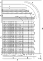
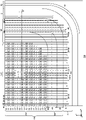
- FIG. 1 is a top view showing an example of a semiconductor device 100;
- FIG. 2 is an enlarged view of a region D in FIG. 1;
- FIG. FIG. 3 is a diagram showing an example of an ee cross section in FIG. 2;
- FIG. 3 is a diagram showing an example of the ff cross section in FIG. 2;
- FIG. 3 is a diagram showing an example of a gg cross section in FIG. 2;
- FIG. 3 is a diagram showing another example of the ee cross section in FIG. 2;
- It is a figure which shows an example of the semiconductor device 200 which concerns on a comparative example.
- FIG. 4 is a diagram showing the relationship between the forward current of the FWD and the slope of the reverse recovery voltage at room temperature;
- FIG. 4 is a diagram showing the relationship between the maximum value of the slope of the reverse recovery voltage of the FWD (at low current at room temperature) and the turn-on loss (at rated current at high temperature);
- 3 is a diagram showing IV characteristics of collector current and collector voltage when the gate voltage of the semiconductor devices 100 and 200 is 0 V (OFF);
- FIG. FIG. 4 is a diagram showing IV characteristics of collector currents and collector voltages of the semiconductor device 100 and the semiconductor device 300 when the gate voltage is 15 V (ON); It is a top view which shows an example of the semiconductor device 400 which concerns on other embodiment.
- FIG. 14 is a diagram showing an example of the hh cross section in FIG.
- FIG. 14 is a diagram showing an example of the ii section in FIG. 13;
- FIG. 14 is a diagram showing an example of a jj cross section in FIG. 13;
- It is a top view which shows an example of the semiconductor device 500 which concerns on other embodiment.
- It is a top view which shows an example of the semiconductor device 600 which concerns on other embodiment.
- FIG. 19 is a diagram showing an example of a kk cross section in FIG. 18; It is a top view which shows an example of the semiconductor device 700 which concerns on other embodiment.
- FIG. 21 is a diagram showing an example of an ll cross section in FIG. 20; It is a top view which shows an example of the semiconductor device 800 which concerns on other embodiment.
- FIG. 23 is a diagram showing an example of an mm section in FIG.
- FIG. 25 is a diagram showing an example of the nn cross section in FIG. 24;
- FIG. 25 is a diagram showing an example of an oo cross section in FIG. 24;
- FIG. 25 is a diagram showing an example of a pp cross section in FIG. 24;
- FIG. 25 is a diagram showing another example of the nn cross section in FIG. 24;
- one side in the direction parallel to the depth direction of the semiconductor substrate is called “upper”, and the other side is called “lower”.
- One of the two main surfaces of a substrate, layer or other member is called the upper surface and the other surface is called the lower surface.
- the directions of “up” and “down” are not limited to the direction of gravity or the direction when the semiconductor device is mounted.
- the Cartesian coordinate axes only specify the relative positions of the components and do not limit any particular orientation.
- the Z axis does not limit the height direction with respect to the ground.
- the +Z-axis direction and the ⁇ Z-axis direction are directions opposite to each other.
- the Z-axis direction is described without indicating positive or negative, it means a direction parallel to the +Z-axis and -Z-axis.
- orthogonal axes parallel to the upper and lower surfaces of the semiconductor substrate are defined as the X-axis and the Y-axis.
- the axis perpendicular to the upper and lower surfaces of the semiconductor substrate is defined as the Z-axis.
- the Z-axis direction may be referred to as the depth direction.
- a direction parallel to the upper and lower surfaces of the semiconductor substrate, including the X-axis and Y-axis may be referred to as a horizontal direction.
- the region from the center of the semiconductor substrate in the depth direction to the upper surface of the semiconductor substrate may be referred to as the upper surface side.
- the region from the center of the semiconductor substrate in the depth direction to the bottom surface of the semiconductor substrate may be referred to as the bottom surface side.
- the conductivity type of the doping region doped with impurities is described as P-type or N-type.
- impurities may specifically refer to either N-type donors or P-type acceptors, and may also be referred to as dopants.
- doping means introducing donors or acceptors into a semiconductor substrate to make it a semiconductor exhibiting N-type conductivity or a semiconductor exhibiting P-type conductivity.
- doping concentration means the concentration of donors or the concentration of acceptors at thermal equilibrium.
- the net doping concentration means the net concentration including the polarity of charges, where the donor concentration is the concentration of positive ions and the acceptor concentration is the concentration of negative ions.
- the donor concentration is N D and the acceptor concentration is N A
- the net net doping concentration at any location is N D ⁇ N A.
- net doping concentration may be simply referred to as doping concentration.
- a donor has the function of supplying electrons to a semiconductor.
- the acceptor has the function of receiving electrons from the semiconductor.
- Donors and acceptors are not limited to impurities per se.
- VOH defects in which vacancies (V), oxygen (O), and hydrogen (H) are combined in semiconductors function as donors that supply electrons.
- VOH defects are sometimes referred to herein as hydrogen donors.
- references herein to P+ type or N+ type refer to higher doping concentrations than P-type or N-type; references to P-type or N-type refer to higher doping than P-type or N-type. It means that the concentration is low.
- P++ type or N++ type in this specification means that the doping concentration is higher than that of the P+ type or N+ type.
- the unit system in this specification is the SI unit system unless otherwise specified. The unit of length is sometimes displayed in cm, but various calculations may be performed after converting to meters (m).
- chemical concentration refers to the atomic density of impurities measured regardless of the state of electrical activation.
- Chemical concentrations can be measured, for example, by secondary ion mass spectroscopy (SIMS).
- the net doping concentrations mentioned above can be measured by the voltage-capacitance method (CV method).
- the carrier concentration measured by the spreading resistance measurement method (SR method) may be used as the net doping concentration.
- the carrier concentration measured by the CV method or SR method may be a value in thermal equilibrium.
- the donor concentration is sufficiently higher than the acceptor concentration in the N-type region, the carrier concentration in the region may be used as the donor concentration.
- the carrier concentration in that region may be used as the acceptor concentration.
- the doping concentration of the N-type regions is sometimes referred to herein as the donor concentration
- the doping concentration of the P-type regions is sometimes referred to as the acceptor concentration.
- the peak value may be taken as the concentration of donors, acceptors or net doping in the region.
- the average concentration of donors, acceptors or net doping in the region may be used as the concentration of donors, acceptors or net doping.
- atoms/cm 3 or /cm 3 are used to express concentration per unit volume. This unit is used for donor or acceptor concentrations, or chemical concentrations, within a semiconductor substrate. The atoms notation may be omitted.
- the carrier concentration measured by the SR method may be lower than the donor or acceptor concentration.
- the carrier mobility of the semiconductor substrate may be lower than the value in the crystalline state. A decrease in carrier mobility is caused by scattering of carriers due to disorder of the crystal structure due to lattice defects or the like.
- the donor or acceptor concentration calculated from the carrier concentration measured by the CV method or the SR method may be lower than the chemical concentration of the element representing the donor or acceptor.
- the donor concentration of phosphorus or arsenic as a donor or the acceptor concentration of boron (boron) as an acceptor in a silicon semiconductor is about 99% of these chemical concentrations.
- the donor concentration of hydrogen serving as a donor in a silicon semiconductor is about 0.1% to 10% of the chemical concentration of hydrogen.
- Each concentration herein may be a value at room temperature. As an example of the value at room temperature, the value at 300 K (Kelvin) (approximately 26.9° C.) may be used.
- FIG. 1 is a top view showing an example of a semiconductor device 100.
- FIG. FIG. 1 shows the positions of each member projected onto the upper surface of the semiconductor substrate 10 .
- FIG. 1 only some members of the semiconductor device 100 are shown, and some members are omitted.
- a semiconductor device 100 includes a semiconductor substrate 10 .
- the semiconductor substrate 10 is a substrate made of a semiconductor material.
- the semiconductor substrate 10 is a silicon substrate, but the material of the semiconductor substrate 10 is not limited to silicon.
- the semiconductor substrate 10 has an edge 162 when viewed from above.
- simply referring to a top view means viewing from the top side of the semiconductor substrate 10 .
- the semiconductor substrate 10 of this example has two sets of edges 162 facing each other when viewed from above.
- the X-axis and Y-axis are parallel to one of the edges 162 .
- the Z-axis is perpendicular to the upper surface of the semiconductor substrate 10 .
- An active portion 160 is provided on the semiconductor substrate 10 .
- the active portion 160 is a region through which a main current flows in the depth direction between the upper and lower surfaces of the semiconductor substrate 10 when the semiconductor device 100 operates.
- An emitter electrode is provided above the active portion 160, but is omitted in FIG.
- the active section 160 is provided with a transistor section 70 including transistor elements such as IGBTs.
- transistor sections 70 and diode sections including diode elements such as FWD (Free Wheel Diode) may be alternately arranged along a predetermined arrangement direction on the upper surface of semiconductor substrate 10 .
- the transistor section 70 has a P+ type collector region in a region in contact with the lower surface of the semiconductor substrate 10 .
- a gate structure having an N++ type emitter region, a P ⁇ type base region, a gate conductive section and a gate insulating film is periodically arranged on the upper surface side of the semiconductor substrate 10.
- the semiconductor device 100 may have one or more pads above the semiconductor substrate 10 .
- the semiconductor device 100 of this example has a gate pad 164 .
- Semiconductor device 100 may have pads such as an anode pad, a cathode pad, and a current sensing pad. Each pad is arranged near the edge 162 .
- the vicinity of the edge 162 refers to a region between the edge 162 and the emitter electrode in top view.
- each pad may be connected to an external circuit via a wiring such as a wire.
- a gate potential is applied to the gate pad 164 .
- Gate pad 164 is electrically connected to the conductive portion of the gate trench portion of active portion 160 .
- the semiconductor device 100 includes a gate wiring 130 connecting the gate pad 164 and the gate trench portion. In FIG. 1, the gate wiring 130 is hatched with oblique lines.
- the gate wiring 130 is arranged between the active portion 160 and the edge 162 of the semiconductor substrate 10 when viewed from above.
- the gate wiring 130 of this example surrounds the active portion 160 when viewed from above.
- a region surrounded by the gate wiring 130 in top view may be the active portion 160 .
- the gate wiring 130 is connected to the gate pad 164 .
- the gate wiring 130 is arranged above the semiconductor substrate 10 .
- the gate wiring 130 may be a metal wiring containing aluminum or the like.
- the outer well region 11 is provided so as to overlap with the gate wiring 130 . In other words, like the gate wiring 130, the outer well region 11 surrounds the active portion 160 when viewed from above. The outer well region 11 is also provided to extend with a predetermined width in a range that does not overlap with the gate wiring 130 .
- the outer well region 11 is a region of the second conductivity type.
- the peripheral well region 11 in this example is of P+ type (see FIG. 2).
- the impurity concentration of outer well region 11 may be 5.0 ⁇ 10 17 atoms/cm 3 or more and 5.0 ⁇ 10 19 atoms/cm 3 or less.
- the impurity concentration of outer well region 11 may be 2.0 ⁇ 10 18 atoms/cm 3 or more and 2.0 ⁇ 10 19 atoms/cm 3 or less.
- the semiconductor device 100 also includes a temperature sensing portion (not shown), which is a PN junction diode made of polysilicon or the like, and a current detecting portion (not shown) that simulates the operation of the transistor portion 70 provided in the active portion 160.
- a temperature sensing portion (not shown), which is a PN junction diode made of polysilicon or the like, and a current detecting portion (not shown) that simulates the operation of the transistor portion 70 provided in the active portion 160.
- the semiconductor device 100 of this example includes an edge termination structure portion 90 between the active portion 160 and the edge 162 when viewed from above.
- the edge termination structure 90 in this example is located between the peripheral gate line 130 and the edge 162 .
- the edge termination structure 90 reduces electric field concentration on the upper surface side of the semiconductor substrate 10 .
- Edge termination structure 90 may include at least one of a guard ring, a field plate, and a resurf annularly surrounding active portion 160 .
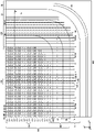
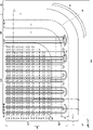
- FIG. 2 is an enlarged view of area D in FIG.
- a region D is a region including the transistor section 70 .
- the semiconductor device 100 of this example includes a gate trench portion 40 , a dummy trench portion 30 , an outer peripheral well region 11 , an emitter region 12 and a contact region 15 provided inside the upper surface side of the semiconductor substrate 10 .
- Each of the gate trench portion 40 and the dummy trench portion 30 is an example of the trench portion.
- the semiconductor device 100 of this example includes emitter electrodes and gate wirings 130 provided above the upper surface of the semiconductor substrate 10 .
- the emitter electrode and gate line 130 are provided separately from each other.
- An interlayer insulating film is provided between the emitter electrode/gate wiring 130 and the upper surface of the semiconductor substrate 10 .
- the emitter electrode, gate wiring 130 and interlayer insulating film are omitted.
- the emitter electrode is provided above the gate trench portion 40 , the dummy trench portion 30 , the outer peripheral well region 11 , the emitter region 12 and the contact region 15 .
- the emitter electrode contacts emitter region 12 and contact region 15 on the upper surface of semiconductor substrate 10 through contact holes.
- the emitter electrode is connected to the dummy conductive portion in the dummy trench portion 30 through a contact hole provided in the interlayer insulating film.
- the emitter electrode may be connected to the dummy conductive portion of the dummy trench portion 30 at the tip portion 31 of the dummy trench portion 30 in the Y-axis direction.
- the gate wiring 130 is connected to the gate trench portion 40 through a contact hole provided in the interlayer insulating film.
- the gate wiring 130 may be connected to the gate conductive portion of the gate trench portion 40 at the tip portion 41 of the gate trench portion 40 in the Y-axis direction. Gate wiring 130 is not connected to the dummy conductive portion in dummy trench portion 30 .
- the emitter electrode is made of a material containing metal.
- at least a partial region of the emitter electrode is made of aluminum or a metal alloy such as an aluminum-silicon alloy such as AlSi, AlSiCu.
- the emitter electrode may have a barrier metal made of titanium, a titanium compound, or the like under the region made of aluminum or the like.
- the contact hole may have a plug formed by embedding tungsten or the like so as to be in contact with the barrier metal and the aluminum or the like.
- the transistor section 70 has a plurality of trench sections arranged in the arrangement direction.
- trench portions are provided in the active portion 160 and the outer well region 11 on the upper surface of the semiconductor substrate 10 .
- the trench portions are provided in a stripe shape in the top view of the transistor portion 70 .
- one or more gate trench sections 40 and one or more dummy trench sections 30 are alternately provided along the arrangement direction.
- one gate trench portion 40 and two dummy trench portions 30 are alternately provided.
- the gate trench portion 40 of this example connects the two straight portions 39 extending along the extending direction perpendicular to the arrangement direction (the portion of the trench that is linear along the extending direction) and the two straight portions 39 . It may have a tip 41 .
- the stretching direction in FIG. 2 is the Y-axis direction.
- At least a portion of the tip portion 41 is preferably provided in a curved shape when viewed from above.
- the dummy trench portions 30 are provided between the respective straight portions 39 of the gate trench portions 40 .
- One dummy trench portion 30 may be provided between the straight portions 39, or a plurality of dummy trench portions 30 may be provided.
- two dummy trench portions 30 are provided between each straight portion 39 .
- the dummy trench portion 30 may have a linear shape extending in the extending direction, and may have a linear portion 29 and a tip portion 31 like the gate trench portion 40 .
- each dummy trench portion 30 has a straight portion 29 and a tip portion 31 .
- the diffusion depth of the outer peripheral well region 11 may be deeper than the depths of the gate trench portion 40 and the dummy trench portion 30 .
- Y-axis direction ends of the gate trench portion 40 and the dummy trench portion 30 are provided in the outer peripheral well region 11 when viewed from above. That is, the bottom of each trench in the depth direction is covered with the outer well region 11 at the end of each trench in the Y-axis direction. As a result, electric field concentration at the bottom of each trench can be relaxed.
- the semiconductor device 100 may include the gate trench portion 40 or the dummy trench portion 30 that is entirely provided in the outer peripheral well region 11 when viewed from above.
- a mesa portion is provided between each trench portion in the arrangement direction.
- the mesa portion refers to a region sandwiched between trench portions inside the semiconductor substrate 10 .
- the upper end of the mesa portion is the upper surface of the semiconductor substrate 10 .
- the depth position of the lower end of the mesa portion is the same as the depth position of the lower end of the trench portion.
- the mesa portion of this example extends in the extension direction (Y-axis direction) along the trench on the upper surface of the semiconductor substrate 10 .
- the transistor section 70 is provided with the mesa section 60 .
- Each mesa portion 60 may be provided with at least one of the first conductivity type emitter region 12 and the second conductivity type contact region 15 .
- the emitter region 12 in this example is of N++ type and the contact region 15 is of P++ type.
- the emitter region 12 and the contact region 15 may be provided between the base region and the upper surface of the semiconductor substrate 10 in the depth direction.
- the mesa portion 60 of the transistor portion 70 has the emitter region 12 exposed on the upper surface of the semiconductor substrate 10 .
- the emitter region 12 is provided in contact with the gate trench portion 40 .
- the mesa portion 60 in contact with the gate trench portion 40 may be provided with the contact region 15 exposed to the upper surface of the semiconductor substrate 10 .
- the contact region 15 is exposed on the upper surface of the semiconductor substrate 10 in the mesa portion 60 and arranged closest to the gate wiring 130 .
- Each of the contact region 15 and the emitter region 12 in the mesa portion 60 is provided from one trench portion to the other trench portion in the X-axis direction.
- the contact regions 15 and the emitter regions 12 of the mesa portion 60 are alternately arranged along the extension direction (Y-axis direction) of the trench portion.
- the contact regions 15 and the emitter regions 12 of the mesa portion 60 may be provided in stripes along the extending direction (Y-axis direction) of the trench portion.
- an emitter region 12 is provided in a region in contact with the trench portion, and a contact region 15 is provided in a region sandwiched between the emitter regions 12 .
- the edge termination structure 90 is provided with a guard ring 92 .
- Edge termination structure 90 may be provided with a plurality of guard rings 92 .
- the impurity concentration of guard ring 92 may be the same as that of outer well region 11 .
- the active portion 160 has a central portion 170 and an outer peripheral portion 180 .
- Central portion 170 has emitter region 12 .
- Peripheral portion 180 surrounds central portion 170 .
- the outer peripheral portion 180 surrounds the central portion 170 in top view.
- the boundary between the central portion 170 and the outer peripheral portion 180 may be the emitter region 12 closest to the outer peripheral well region 11 in the X-axis direction or the Y-axis direction.
- a contact hole is provided above each mesa portion 60 of the central portion 170 .
- the contact hole in this example is provided above each region of the contact region 15 and the emitter region 12 .
- the contact hole may be arranged in the center of the mesa portion 60 in the arrangement direction (X-axis direction). In this example, contact holes are omitted.
- FIG. 2 shows an active-side bottom region 182 and an outer peripheral-side bottom region 184 provided in the semiconductor substrate 10 .
- An active bottom region 182 is provided in the central portion 170 .
- the outer peripheral side bottom region 184 is provided in the outer peripheral portion 180 . As shown in FIG. 2, the active side bottom region 182 and the perimeter side bottom region 184 are spaced apart.
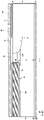
- FIG. 3 is a diagram showing an example of the ee cross section in FIG.
- the ee section is the XZ plane passing through the emitter region 12 of the central portion 170 . Note that the dimensions in FIG. 3 do not necessarily match the dimensions in FIG.
- the semiconductor device 100 of this example has a semiconductor substrate 10, an interlayer insulating film 38, an emitter electrode 52, a collector electrode 24 and a gate wiring 130 in the cross section.
- the interlayer insulating film 38 is provided on the upper surface 21 of the semiconductor substrate 10 .
- the interlayer insulating film 38 is a film including at least one layer of an insulating film such as silicate glass doped with an impurity such as boron or phosphorus, a thermal oxide film, and other insulating films.
- the contact hole 54 described with reference to FIG. 2 is provided in the interlayer insulating film 38 .
- a contact hole 54 is partially provided above the outer well region 11 to connect the outer well region 11 to the emitter electrode.
- the emitter electrode 52 is provided above the interlayer insulating film 38 . Emitter electrode 52 is in contact with top surface 21 of semiconductor substrate 10 through contact hole 54 in interlayer insulating film 38 . Note that the emitter electrode 52 may be provided above the outer peripheral well region 11 . A gate wiring 130 may be provided above the outer well region 11 . A gate polysilicon 46 may be provided under the gate wiring 130 .
- the collector electrode 24 is provided on the bottom surface 23 of the semiconductor substrate 10 .
- Emitter electrode 52 and collector electrode 24 are made of a metal material such as aluminum.
- the direction (Z-axis direction) connecting the emitter electrode 52 and the collector electrode 24 is referred to as the depth direction.
- Each mesa portion 60 is provided with a base region 14 of the second conductivity type.
- Emitter region 12 and contact region 15 are provided between top surface 21 of semiconductor substrate 10 and base region 14 .
- the base region 14 in this example is P-type.
- the semiconductor substrate 10 has a first conductivity type drift region 18 .
- the drift region 18 in this example is N-type or N-type.
- the N++ type emitter region 12 and the P ⁇ type base region 14 are provided in order from the upper surface 21 side of the semiconductor substrate 10. As shown in FIG. A drift region 18 is provided below the base region 14 .
- the mesa portion 60 may be provided with an N+ type accumulation region 16 . Accumulation region 16 is disposed between base region 14 and drift region 18 .
- the emitter region 12 is exposed on the upper surface 21 of the semiconductor substrate 10 and provided in contact with the gate trench portion 40 .
- the emitter region 12 may be in contact with trench portions on both sides of the mesa portion 60 .
- Emitter region 12 has a higher doping concentration than drift region 18 .
- a base region 14 is provided below the emitter region 12 .
- the base region 14 in this example is provided in contact with the emitter region 12 .
- the base region 14 may contact trench portions on both sides of the mesa portion 60 .
- the impurity concentration peak of the base region 14 is, for example, 2.5 ⁇ 10 17 atoms/cm 3 .
- the impurity concentration of base region 14 may be 5.0 ⁇ 10 16 atoms/cm 3 or more and 1.0 ⁇ 10 18 atoms/cm 3 or less.
- the accumulation region 16 is provided below the base region 14 .
- the accumulation region 16 is an N+ type region with a higher doping concentration than the drift region 18 .
- Accumulation region 16 may have a concentration peak of donors, such as phosphorus or hydrogen donors.
- IE effect carrier injection promoting effect
- the accumulation region 16 may be provided so as to cover the entire bottom surface of the base region 14 in each mesa portion 60 .
- the P++ type contact region 15 and the P ⁇ type base region 14 are provided in order from the upper surface 21 side of the semiconductor substrate 10. As shown in FIG. A drift region 18 is provided below the base region 14 .
- the accumulation region 16 may be provided in the mesa portion 60 of the outer peripheral portion 180 .
- An N+ type buffer region 20 may be provided under the drift region 18 .
- the doping concentration of buffer region 20 is higher than the doping concentration of drift region 18 .
- Buffer region 20 may have a concentration peak with a higher doping concentration than drift region 18 .
- the doping concentration of the concentration peak refers to the doping concentration at the apex of the concentration peak.
- an average value of doping concentrations in a region where the doping concentration distribution is substantially flat may be used as the doping concentration of the drift region 18.
- the buffer region 20 may be formed by ion-implanting hydrogen (protons) or an N-type dopant such as phosphorus.
- the buffer region 20 of this example is formed by implanting hydrogen ions.
- the buffer region 20 may function as a field stop layer that prevents the depletion layer extending from the bottom end of the base region 14 from reaching the P+ type collector region 22 .
- a P+ type collector region 22 is provided under the buffer region 20 .
- the acceptor concentration of collector region 22 is higher than the acceptor concentration of base region 14 .
- Collector region 22 may contain the same acceptor as base region 14 or may contain a different acceptor.
- the acceptor of the collector region 22 is boron, for example. Elements that serve as acceptors are not limited to the above examples.
- the collector region 22 is exposed on the bottom surface 23 of the semiconductor substrate 10 and connected to the collector electrode 24 .
- Collector electrode 24 may contact the entire bottom surface 23 of semiconductor substrate 10 .
- Emitter electrode 52 and collector electrode 24 are made of a metal material such as aluminum.
- One or more gate trench portions 40 and one or more dummy trench portions 30 are provided on the upper surface 21 side of the semiconductor substrate 10 .
- Each trench extends from the upper surface 21 of the semiconductor substrate 10 through the base region 14 and reaches the drift region 18 .
- the contact region 15 and/or the accumulation region 16 are provided, each trench also passes through these doping regions and reaches the drift region 18.
- FIG. The fact that the trench penetrates the doping region is not limited to the order of forming the doping region and then forming the trench.
- a structure in which a doping region is formed between the trench portions after the trench portions are formed is also included in the structure in which the trench portion penetrates the doping regions.
- the gate trench portion 40 has a gate trench provided in the upper surface 21 of the semiconductor substrate 10, a gate insulating film 42 and a gate conductive portion 44.
- a gate insulating film 42 is provided to cover the inner wall of the gate trench.
- the gate insulating film 42 may be formed by oxidizing or nitriding the semiconductor on the inner wall of the gate trench.
- the gate conductive portion 44 is provided inside the gate insulating film 42 inside the gate trench. That is, the gate insulating film 42 insulates the gate conductive portion 44 and the semiconductor substrate 10 from each other.
- the gate conductive portion 44 is formed of a conductive material such as polysilicon.
- the gate conductive portion 44 may be provided longer than the base region 14 in the depth direction.
- the gate trench portion 40 in the cross section is covered with the interlayer insulating film 38 on the upper surface 21 of the semiconductor substrate 10 .
- the gate conductive portion 44 is electrically connected to the gate wiring 130 .
- a predetermined gate voltage is applied to the gate conductive portion 44 , a channel is formed by an electron inversion layer in the surface layer of the interface contacting the gate trench portion 40 in the base region 14 .
- the dummy trench portion 30 may have the same structure as the gate trench portion 40 in the cross section.
- the dummy trench section 30 has a dummy trench provided in the upper surface 21 of the semiconductor substrate 10 , a dummy insulating film 32 and a dummy conductive section 34 .
- the dummy conductive portion 34 is electrically connected to the emitter electrode 52 .
- a dummy insulating film 32 is provided to cover the inner wall of the dummy trench.
- the dummy conductive portion 34 is provided inside the dummy trench and inside the dummy insulating film 32 .
- the dummy insulating film 32 insulates the dummy conductive portion 34 from the semiconductor substrate 10 .
- the dummy conductive portion 34 may be made of the same material as the gate conductive portion 44 .
- the dummy conductive portion 34 is made of a conductive material such as polysilicon.
- the dummy conductive portion 34 may have the same length as the gate conductive portion 44 in the depth direction.
- the gate trench portion 40 and the dummy trench portion 30 of this example are covered with an interlayer insulating film 38 on the upper surface 21 of the semiconductor substrate 10 .
- the bottoms of the dummy trench portion 30 and the gate trench portion 40 may be curved (curved in cross section) convex downward.
- the semiconductor device 100 of this example is an IGBT, which is operated as a switching element in combination with a diode such as an FWD. Depending on the application, it is necessary to suppress the slope of the reverse recovery voltage of the FWD at low current and reduce noise.
- the semiconductor device 200 according to the comparative example when the external gate resistance connected to the gate conductive portion 44 is increased in order to suppress the slope of the reverse recovery voltage, the turn-on speed of the IGBT slows down at the rated current, and the turn-on loss decreases. Increase.
- the bottom region of the second conductivity type is provided at the bottom of the trench.
- the central portion 170 is provided with an active side bottom region 182 of the second conductivity type at the bottom of the trench portion.
- Active side bottom region 182 in this example is P-type.
- An active side bottom region 182 covers the bottom of the trench.
- An active side bottom region 182 spans the bottom of at least two trench portions.
- An active side bottom region 182 may be provided below the base region 14 .
- the provision of the second conductivity type active-side bottom region 182 makes it easier to control the slope of the reverse recovery voltage of the FWD. Therefore, turn-on loss can be reduced. Also, the breakdown voltage can be improved by providing the active-side bottom region 182 .
- the outer peripheral portion 180 is provided with an outer peripheral side bottom region 184 of the second conductivity type at the bottom of the trench portion.
- the outer bottom region 184 in this example is P-type.
- the outer bottom region 184 covers the bottom of the trench.
- the outer bottom region 184 may be provided toward the active bottom region 182 . That is, the outer peripheral side bottom region 184 may be provided at the same depth as the active side bottom region 182 in the depth direction of the semiconductor substrate 10 .
- the outer peripheral side bottom region 184 is electrically connected to the outer peripheral well region 11 . In this example, the outer bottom region 184 is directly connected to the outer well region 11 . Therefore, the electric field concentration at the boundary between the outer peripheral well region 11 and the outer peripheral side bottom region 184 can be alleviated, and the avalanche resistance at the time of turn-off can be improved.
- the active side bottom region 182 and the outer peripheral side bottom region 184 are provided apart. That is, at least part of the outer peripheral portion 180 is not provided with a bottom region. Since the active-side bottom region 182 and the outer peripheral-side bottom region 184 are provided apart from each other, it is possible to prevent the active-side bottom region 182 and the outer peripheral well region 11 from having the same potential. Therefore, it is possible to prevent the semiconductor device 100 from failing to operate.
- Active side bottom region 182 may be electrically floating. Active-side bottom region 182 is said to be electrically floating if it is not electrically connected to any electrode. Also, the active-side bottom region 182 may not be partially provided in the active portion 160 . That is, the active-side bottom region 182 does not have to be provided over the entire active portion 160 .
- the active-side bottom region 182 may also be provided in the outer peripheral portion 180 . That is, the active-side bottom region 182 is provided wider than the range in which the emitter regions 12 are provided in the arrangement direction of the trench portions.
- the active-side bottom region 182 may be provided on at least a portion of the outer peripheral portion 180 .
- the concentration of the base region 14 changes, and the threshold value of the semiconductor device 100 fluctuates. Therefore, by providing the emitter region 12 only at the portion where the concentration of the base region 14 is changed, the fluctuation of the threshold value can be suppressed. If the active-side bottom region 182 is provided over the entire outer peripheral portion 180 , the active-side bottom region 182 will be connected to the outer peripheral well region 11 . Therefore, it is preferable that the active-side bottom region 182 is not provided in at least a portion of the outer peripheral portion 180 .
- the bottom region may terminate at the bottom of the trench. That is, the bottom region does not terminate at mesa 60 .
- the active side bottom region 182 terminates at the bottom of the trench.
- the outer peripheral bottom region 184 terminates at the bottom of the trench.
- the impurity concentration of the active-side bottom region 182 and the outer-peripheral-side bottom region 184 may be the same. By making the impurity concentration of the active-side bottom region 182 and the outer-peripheral-side bottom region 184 the same, the manufacturing process can be made the same. Also, the impurity concentration of the outer peripheral side bottom region 184 may be higher than the impurity concentration of the active side bottom region 182 . By making the impurity concentration of the outer peripheral side bottom region 184 higher than the impurity concentration of the active side bottom region 182, the effect of alleviating local electric field concentration is enhanced. The impurity concentration of the outer peripheral well region 11 may be higher than the impurity concentration of the outer peripheral side bottom region 184 .
- the impurity concentration peak of each bottom region is, for example, 4.0 ⁇ 10 15 atoms/cm 3 .
- the impurity concentration peak of each bottom region may be 3.0 ⁇ 10 14 atoms/cm 3 or more and 3.0 ⁇ 10 16 atoms/cm 3 or less.
- the dose of ions implanted into each bottom region may be 1.0 ⁇ 10 11 ion/cm 2 or more and 1.0 ⁇ 10 13 ion/cm 2 or less.
- the distance L between the active-side bottom region 182 and the outer-peripheral-side bottom region 184 in the arrangement direction of the trench portions may be equal to or greater than the pitch width W1 of the trench portions.
- the pitch width W1 of the trench portion is the distance from the center of the conductive portion of the trench portion to the center of the conductive portion of the adjacent trench portion.
- a distance L between the active-side bottom region 182 and the outer-peripheral-side bottom region 184 in the arrangement direction of the trench portions may preferably be twice or more the pitch width W1 of the trench portions.
- a distance L between the active-side bottom region 182 and the outer-peripheral-side bottom region 184 in the arrangement direction of the trench portions may be 20 times or less the pitch width W1 of the trench portions. By doing so, the range in which the active-side bottom region 182 is provided can be widened.
- a distance L between the active-side bottom region 182 and the outer-peripheral-side bottom region 184 in the arrangement direction of the trench portions may preferably be six times or less the pitch width W1 of the trench portions.
- the distance L between the active-side bottom region 182 and the outer-peripheral-side bottom region 184 in the arrangement direction of the trench portions is five times the pitch width W1 of the trench portions. Also, the distance L may be 10 to 15 times the pitch width W1 of the trench portion.
- the distance L in the arrangement direction between the active-side bottom region 182 and the outer peripheral-side bottom region 184 may be 2 ⁇ m or more.
- a distance L in the arrangement direction between the active-side bottom region 182 and the outer peripheral-side bottom region 184 may preferably be 4 ⁇ m or more.
- a distance L in the arrangement direction between the active-side bottom region 182 and the outer peripheral-side bottom region 184 may be 40 ⁇ m or less.
- a distance L in the arrangement direction between the active-side bottom region 182 and the outer peripheral-side bottom region 184 may preferably be 12 ⁇ m or less.
- a distance L in the arrangement direction between the active-side bottom region 182 and the outer peripheral-side bottom region 184 is, for example, 10 ⁇ m. Also, the distance L may be 30 ⁇ m or more and 35 ⁇ m or less.
- the outer peripheral side bottom region 184 may be provided in a range from the outer peripheral well region 11 to five times or less the pitch width W1 of the trench portions in the arrangement direction of the trench portions.
- the outer peripheral side bottom region 184 is provided in a range of three times or less the pitch width W1 of the trench portions from the outer peripheral well region 11 in the arrangement direction of the trench portions.
- the active-side bottom region 182 and the outer peripheral-side bottom region 184 can be sufficiently separated, and the semiconductor device 100 can be prevented from not operating.
- the distance L in the arrangement direction between the active-side bottom region 182 and the outer peripheral-side bottom region 184 may be larger than the width W2 in which the outer peripheral-side bottom region 184 is provided.
- the width W2 of the outer peripheral side bottom region 184 is, for example, 7 ⁇ m.
- a gate trench portion 40 is preferably provided between the active side bottom region 182 and the outer peripheral side bottom region 184 in the depth direction of the semiconductor substrate 10 .
- the presence of the gate trench portion 40 between the active-side bottom region 182 and the outer peripheral-side bottom region 184 in the depth direction of the semiconductor substrate 10 can suppress the influence of the ground potential.
- the distance L in the arrangement direction of the trench portions between the active-side bottom region 182 and the outer peripheral-side bottom region 184 is equal to the gate trench portion.
- the ratio of 40 to the dummy trench portion 30 is 1:2, it may be three times or more the pitch width W1 of the trench portions. Further, in this case, when the ratio of the gate trench portion 40 and the dummy trench portion 30 is 1:X, the distance L may be 1+X times or more.
- the distance L in the arrangement direction of the trench portions should be equal to or greater than the pitch width W1 of the trench portions.
- the distance L in the arrangement direction of the trench portions between the active-side bottom region 182 and the outer peripheral-side bottom region 184 is equal to the gate trench portion.
- the ratio of 40 to dummy trench portion 30 is 1:2, it is sufficient that the pitch width W1 of the trench portion is at least twice. In this case, when the ratio of the gate trench portion 40 to the dummy trench portion 30 is 1:X, the distance L may be X times or more.
- the accumulation region 16 is preferably provided wider than the active-side bottom region 182 .
- the accumulation region 16 is provided wider than the active-side bottom region 182 in the X-axis direction. With such a configuration, the accumulation region 16 and the active-side bottom region 182 can be easily formed.
- the storage region 16 does not overlap the bottom region 184 on the outer peripheral side in the depth direction.
- FIG. 4 is a diagram showing an example of the ff section in FIG.
- the ff cross section is the YZ plane passing through the tip portion 41 of the gate trench portion 40 and the tip portion 31 of the dummy trench portion 30 . Note that the dimensions in FIG. 4 do not necessarily match the dimensions in FIG.
- the semiconductor device 100 of this example has a semiconductor substrate 10, an interlayer insulating film 38, an emitter electrode 52, a collector electrode 24 and a gate wiring 130 in the cross section.
- the gate trench portion 40 is connected to the gate wiring 130 .
- the dummy trench portion 30 is connected to the emitter electrode 52 through the contact hole 56 .
- a dummy polysilicon 36 may be provided under the emitter electrode 52 .
- the outer peripheral side bottom region 184 may be provided at the same depth as the active side bottom region 182 in the depth direction of the semiconductor substrate 10, as in FIG.
- FIG. 5 is a diagram showing an example of a gg section in FIG.
- the gg section is the YZ plane passing through the straight portion 29 of the dummy trench portion 30 .
- the semiconductor device 100 of this example has a semiconductor substrate 10, an interlayer insulating film 38, an emitter electrode 52, a collector electrode 24 and a gate wiring 130 in the cross section.
- an interlayer insulating film 38 is provided between the emitter electrode 52 and the dummy trench portion 30 .
- the outer peripheral side bottom region 184 may be provided at the same depth as the active side bottom region 182 in the depth direction of the semiconductor substrate 10 .
- FIG. 6 is a diagram showing another example of the ee cross section in FIG. FIG. 6 is different from FIG. 2 in that the outer peripheral side bottom region 184 is provided wider than the active side bottom region 182 in the depth direction of the semiconductor substrate 10 . Otherwise, the configuration of FIG. 6 may be the same as that of FIG. In this example, the outer bottom region 184 is wider on the lower surface 23 side than the active bottom region 182 and has substantially the same depth as the outer well region 11 . Since the outer peripheral side bottom region 184 is wider than the active side bottom region 182, the electric field distribution can be adjusted.
- FIG. 7 is a diagram showing an example of a semiconductor device 200 according to a comparative example.
- FIG. 7 differs from FIG. 3 in that the active side bottom region 182 and the outer peripheral side bottom region 184 are not provided.
- Other configurations in FIG. 7 may be the same as in FIG.
- FIG. 8 is a diagram showing an example of a semiconductor device 300 according to a comparative example.
- FIG. 8 differs from FIG. 3 in that the active side bottom region 182 and the outer peripheral side bottom region 184 are connected.
- Other configurations in FIG. 8 may be the same as in FIG.
- the boundary between the active side bottom region 182 and the outer peripheral side bottom region 184 may be the boundary between the central portion 170 and the outer peripheral portion 180 .
- FIG. 9 is a diagram showing the relationship between the forward current of the FWD and the slope of the reverse recovery voltage at room temperature.
- the forward current is shown as a ratio when the rated current is 1.
- the external gate resistance is adjusted so that the slope of the reverse recovery voltage is the same (approximately 5 kV/ ⁇ sec) when the forward current is 5 to 10% (low current). is doing.
- the semiconductor device 100 can keep the slope of the reverse recovery voltage of the FWD at the same level as the semiconductor device 200 even if the forward current is changed. Therefore, when the forward current is 100% (at the rated current), the turn-on speed of the IGBT side does not slow down, and it can be kept as fast as when the forward current is 5 to 10% (at the low current). , turn-on losses can be reduced.
- FIG. 10 is a diagram showing the relationship between the maximum value of the slope of the reverse recovery voltage of the FWD (at low current at room temperature) and the turn-on loss (at rated current at high temperature).
- FIG. 10 can be obtained by plotting the maximum value of the slope of the reverse recovery voltage on the FWD side and the turn-on loss on the IGBT side on a one-to-one basis while changing the external gate resistance. From FIG. 10, when comparing the semiconductor device 100 and the semiconductor device 200 with the maximum value of the slope of the reverse recovery voltage of the FWD being 5 kV/ ⁇ sec, the turn-on loss can be reduced by approximately 50%.
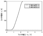
- FIG. 11 is a diagram showing the IV characteristics of the collector current and the collector voltage when the gate voltage of the semiconductor device 100 and the semiconductor device 200 is 0 V (OFF).
- the collector voltage is shown as a ratio when the semiconductor device 200 is set to 1.
- FIG. 12 is a diagram showing IV characteristics of the collector current and the collector voltage when the gate voltage of the semiconductor devices 100 and 300 is 15 V (ON). As shown in FIG. 12, the semiconductor device 300 does not operate when the active side bottom region 182 and the outer peripheral side bottom region 184 are connected.
- FIG. 13 is a top view showing an example of a semiconductor device 400 according to another embodiment.
- the semiconductor device 400 of FIG. 13 differs from the semiconductor device 100 of FIG. 2 in the arrangement of the bottom region 190 . 13 differs from the semiconductor device 100 of FIG. 2 in that an outer peripheral deep trench portion 140 is provided.
- Other configurations of the semiconductor device 400 of FIG. 13 may be the same as those of the semiconductor device 100 of FIG.
- FIG. 13 shows a bottom region 190 provided within the semiconductor substrate 10 .
- the bottom region 190 has an active bottom region 182 (not shown in FIG. 13), an outer peripheral bottom region 184 (not shown in FIG. 13), and an outer intermediate bottom region which will be described later.
- the bottom region 190 does not have to be partially provided in the active portion 160 .
- the bottom region 190 is not partially provided on the perimeter 180 .
- a region where the bottom region 190 is not provided is a bottom-less region 192 .
- the bottomless region 192 is provided at the same depth as the bottom region 190 in the depth direction of the semiconductor substrate 10 .
- a first conductivity type drift region 18 is provided in the bottomless region 192 .
- the bottomless region 192 is provided so as to be in contact with the outer peripheral side deepened trench portion 140 provided closest to the central portion 170 in the arrangement direction (X-axis direction) of the trench portions.
- the bottomless region 192 By arranging the bottomless region 192 in this way, the bottom region 190 (active side bottom region 182) provided in the central portion 170 and the bottom portion provided in the outer peripheral portion 180 in the extending direction (Y-axis direction) of the trench portion It is possible to prevent the region 190 (outer peripheral side bottom region 184) from being connected. Note that the bottomless region 192 may partially overlap the outer peripheral side deepened trench portion 140 .
- the transistor section 70 has a plurality of deepened trench sections arranged in the arrangement direction.
- the trench portion has a deepened trench portion.
- the deepened trench portion is provided in the active portion 160 on the top surface of the semiconductor substrate 10 .
- the deepened trench portion is provided in the outer peripheral portion 180 .
- the deepened trench portion provided in the outer peripheral portion 180 is referred to as the outer peripheral side deepened trench portion 140 .
- the outer peripheral side deepened trench portion 140 may be provided in the outer peripheral well region 11 .
- the outer deep trench portion 140 may not be provided in the central portion 170 .
- the outer peripheral side deepened trench portion 140 is indicated by hatching.
- the outer peripheral side deepened trench portion 140 has a trench provided on the upper surface 21 of the semiconductor substrate 10, an insulating film, and a conductive portion.
- the outer peripheral deepened trench portion 140 may function as a dummy trench portion.
- a conductive portion of the outer peripheral deepened trench portion 140 may be connected to the emitter electrode 52 .
- the outer peripheral deepened trench portion 140 may function as a gate trench portion.
- a conductive portion of the outer deep trench portion 140 may be connected to the gate wiring 130 .
- the outer peripheral deepened trench portion 140 may have two straight portions 49 extending along the extending direction perpendicular to the arrangement direction (trench portions that are linear along the extending direction).
- the outer deep trench portion 140 may have a tip portion 51 connecting the two straight portions 49 .
- At least a part of the tip portion 51 is preferably provided in a curved shape when viewed from above.
- FIG. 14 is a diagram showing an example of the hh cross section in FIG.
- the hh section is the XZ plane passing through the emitter region 12 of the central portion 170 . Note that the dimensions in FIG. 14 do not necessarily match the dimensions in FIG.
- the semiconductor device 400 of this example has the semiconductor substrate 10, the interlayer insulating film 38, the emitter electrode 52, the collector electrode 24, and the gate wiring 130 in the cross section.
- the outer peripheral side deepened trench portion 140 is formed deeper than the bottom region 190 .
- the outer peripheral deepened trench portion 140 may be formed deeper than the gate trench portion 40 .
- the outer peripheral deepened trench portion 140 may be formed deeper than the dummy trench portion 30 .
- the outer peripheral deepened trench portion 140 may be formed deeper than the outer peripheral well region 11 .
- the bottom region 190 can be divided.
- the bottom region 190 provided closer to the central portion 170 than the outer deep trench portion 140 in the arrangement direction of the trench portions is referred to as an active-side bottom region 182 .
- the bottom region 190 provided between the outer deepened trench portions 140 in the arrangement direction of the trench portions is referred to as the outer intermediate bottom region 186 .
- the bottom region 190 provided between the outer deep trench portion 140 and the outer well region 11 in the arrangement direction of the trench portions is referred to as the outer bottom region 184 .
- the outer deep trench portion 140 is provided in the outer peripheral portion 180 between the active side bottom region 182 and the outer peripheral side bottom region 184 in the arrangement direction of the trench portions. Further, the outer peripheral side deepened trench portion 140 is formed deeper than the active side bottom region 182 . The outer deep trench portion 140 is formed deeper than the outer bottom region 184 .
- the active side bottom region 182 can be separated from the outer peripheral side bottom region 184 and the outer peripheral side intermediate bottom region 186, and the active side bottom region 182 can be electrically floating. Therefore, it is possible to improve the controllability of the slope of the reverse recovery voltage. Further, by providing the outer peripheral side bottom region 184 and the outer peripheral side intermediate bottom region 186, the breakdown voltage imbalance of the semiconductor device 400 can be eliminated.
- the impurity concentration of the active-side bottom region 182, the outer-peripheral-side bottom region 184, and the outer-peripheral-side intermediate bottom region 186 may be the same.
- the manufacturing process can be made the same.
- the impurity concentrations of the active-side bottom region 182, the outer-peripheral-side bottom region 184, and the outer-peripheral-side intermediate bottom region 186 may be different. Further, the impurity concentration of the active-side bottom region 182 and the outer peripheral-side bottom region 184 may be the same, and only the impurity concentration of the outer-peripheral-side intermediate bottom region 186 may be different.
- the width W3 of the outer peripheral deepened trench portion 140 in the arrangement direction of the trench portions may be 5.0 ⁇ m or more.
- a width W3 in which the outer peripheral side deepened trench portions 140 are provided in the arrangement direction of the trench portions may be equal to or greater than the pitch width W1 of the trench portions other than the outer peripheral side deepened trench portions 140 .
- the pitch width W1 of the trench portions other than the outer peripheral deepened trench portion 140 may be the same as the pitch width W1 of the trench portions in FIG.
- a width W3 in which the outer peripheral side deepened trench portions 140 are provided in the arrangement direction of the trench portions may be twice or more the pitch width W1 of the trench portions other than the outer peripheral side deepened trench portions 140 .
- the pitch width W4 of the outer peripheral side deepened trench portion 140 may be the same as the pitch width W1 of the trench portions other than the outer peripheral side deepened trench portion 140 .
- the pitch width W4 of the outer peripheral side deepened trench portions 140 is the distance from the center of the conductive portion of the outer peripheral side deepened trench portion 140 to the center of the conductive portion of the adjacent outer peripheral side deepened trench portion 140 .
- the pitch width W4 of the outer peripheral side deepened trench portion 140 may be less than or equal to the pitch width W1 of the trench portions other than the outer peripheral side deepened trench portion 140 .
- the outer peripheral side deepened trench portion 140 is formed deeper than the outer peripheral well region 11 . That is, the depth D1 of the outer peripheral side deepened trench portion 140 may be greater than or equal to the depth D2 of the trench portions other than the outer peripheral side deepened trench portion 140 . Note that if the depth of the outer peripheral side deepened trench portion 140 is too deep, the breakdown voltage may decrease. Therefore, the depth D1 of the outer peripheral side deepened trench portion 140 is preferably not more than twice the depth D2 of the trench portions other than the outer peripheral side deepened trench portion 140 .
- outer peripheral side intermediate bottom region 186 may not be provided. That is, the bottomless regions 192 may be provided between the outer peripheral deepened trench portions 140 in the arrangement direction of the trench portions. By not providing the outer peripheral side intermediate bottom region 186, it becomes easier to separate the active side bottom region 182 and the outer peripheral side bottom region 184 from each other.
- FIG. 15 is a diagram showing an example of the ii section in FIG.
- the ii cross section is the YZ plane passing through the tip portion 41 of the gate trench portion 40 and the tip portion 31 of the dummy trench portion 30 . Note that the dimensions in FIG. 15 do not necessarily match the dimensions in FIG.
- the semiconductor device 400 of this example has the semiconductor substrate 10, the interlayer insulating film 38, the emitter electrode 52, the collector electrode 24, and the gate wiring 130 in the cross section.
- FIG. 15 is the same as FIG. 4 except that the bottomless region 192 is shown in dashed lines.
- FIG. 16 is a diagram showing an example of a jj cross section in FIG.
- the jj cross section is the YZ plane passing through the straight portion 29 of the dummy trench portion 30 . Note that the dimensions in FIG. 16 do not necessarily match the dimensions in FIG.
- the semiconductor device 400 of this example has the semiconductor substrate 10, the interlayer insulating film 38, the emitter electrode 52, the collector electrode 24, and the gate wiring 130 in the cross section.
- FIG. 16 is the same as FIG. 5 except that the bottomless region 192 is shown in dashed lines.
- FIG. 17 is a top view showing an example of a semiconductor device 500 according to another embodiment.
- the semiconductor device 500 of FIG. 17 differs from the semiconductor device 400 of FIG. 13 in the structure of the trench portion.
- Other configurations of the semiconductor device 500 of FIG. 17 may be the same as those of the semiconductor device 400 of FIG.
- each trench does not have a tip. That is, the gate trench portion 40 does not have to have the tip portion 41 .
- the gate trench portion 40 may have only straight portions 39 .
- the dummy trench portion 30 may not have the tip portion 31 .
- the dummy trench portion 30 may have only straight portions 29 .
- the outer peripheral side deepened trench portion 140 may not have the tip portion 51 .
- the outer deep trench portion 140 may have only the straight portion 49 . Since each trench portion does not have a tip portion, the degree of freedom in layout of the trench portion can be increased.
- FIG. 18 is a top view showing an example of a semiconductor device 600 according to another embodiment.
- a semiconductor device 600 of FIG. 18 differs from the semiconductor device 500 of FIG. 17 in that an active-side deepened trench portion 150 is provided.
- Other configurations of the semiconductor device 600 of FIG. 18 may be the same as those of the semiconductor device 500 of FIG.
- the active-side deepened trench portion 150 is a deepened trench portion at least partially provided in the central portion 170 .
- the active-side deepened trench portion 150 may be provided in the outer peripheral well region 11 .
- the active-side deepened trench portion 150 may be provided in the outer peripheral portion 180 .
- the active-side deepened trench portion 150 is hatched like the outer-peripheral-side deepened trench portion 140 .
- the active-side deepened trench section 150 has a trench provided on the upper surface 21 of the semiconductor substrate 10, an insulating film, and a conductive section.
- the active-side deepened trench portion 150 may function as a dummy trench portion.
- a conductive portion of the active-side deepened trench portion 150 may be connected to the emitter electrode 52 .
- the active-side deepened trench portion 150 functioning as the dummy trench portion is the active-side deepened trench portion 150-2.
- the active-side deepened trench portion 150 may function as a gate trench portion.
- a conductive portion of the active-side deepened trench portion 150 may be connected to the gate wiring 130 .
- the active-side deepened trench portion 150 functioning as the gate trench portion is designated as the active-side deepened trench portion 150-1.
- the active-side deepened trench portion 150-1 may extend longer than the active-side deepened trench portion 150-2 in the extending direction of the trench portion.
- FIG. 19 is a diagram showing an example of a kk section in FIG.
- the kk section is the XZ plane passing through the emitter region 12 of the central portion 170 .
- the semiconductor device 600 of this example has the semiconductor substrate 10, the interlayer insulating film 38, the emitter electrode 52, the collector electrode 24, and the gate wiring 130 in the cross section. Part of the semiconductor device 600 is omitted in FIG. In FIG. 19, the description of the reference numerals common to those in FIG. 14 is omitted.
- the active-side deepened trench portion 150 is formed deeper than the bottom region 190 .
- active-side deepened trench portion 150 is formed deeper than active-side bottom region 182 .
- the active-side deepened trench portion 150 may be formed deeper than the gate trench portion 40 .
- the active-side deepened trench portion 150 may be formed deeper than the dummy trench portion 30 .
- the active-side deepened trench portion 150 may be formed deeper than the outer peripheral well region 11 .
- the active-side deepened trench portion 150 may be formed to the same depth as the outer peripheral-side deepened trench portion 140 .
- the bottom region 190 can be divided.
- the bottom regions 190 provided between the active-side deepened trench portions 150 in the arrangement direction of the trench portions are defined as active-side intermediate bottom regions 188 .
- an active side intermediate bottom region 188 can be provided in the central portion 170 . Therefore, an electron passage region can be provided. Therefore, the characteristics of the semiconductor device 600 can be improved.
- FIG. 20 is a top view showing an example of a semiconductor device 700 according to another embodiment.
- the semiconductor device 700 of FIG. 20 differs from the semiconductor device 600 of FIG. 18 in that the active-side deepened trench portions 150 are discretely provided.
- Other configurations of the semiconductor device 700 of FIG. 20 may be the same as those of the semiconductor device 600 of FIG.
- the active-side deepening trench portions 150 are discretely provided in the central portion 170 . That is, the active-side deepened trench portion 150 may not be partially provided in the extending direction. Since the active-side deepened trench portions 150 are discretely provided, the active-side bottom region 182 and the active-side intermediate bottom region 188 can be finely provided. A trench portion having the same depth as that of the gate trench portion 40 or the dummy trench portion 30 may be provided in a region where the active-side deepened trench portion 150 is not provided.
- FIG. 21 is a diagram showing an example of the l-l cross section in FIG.
- the ll section is the XZ plane passing through the emitter region 12 of the central portion 170 .
- the ll cross section is the XZ plane that does not pass through the active-side deepened trench portion 150 . Note that the dimensions in FIG. 21 do not necessarily match the dimensions in FIG.
- the semiconductor device 700 of this example has the semiconductor substrate 10, the interlayer insulating film 38, the emitter electrode 52, the collector electrode 24 and the gate wiring 130 in the cross section. Part of the semiconductor device 700 is omitted in FIG.
- the active-side deepened trench portion 150 is not provided in the ll cross section. Therefore, in the cross section, the active side bottom region 182 is provided in the central portion 170 . Also, in this cross section, the active-side intermediate bottom region 188 is not provided in the central portion 170 .
- FIG. 22 is a top view showing an example of a semiconductor device 800 according to another embodiment.
- the semiconductor device 800 of FIG. 22 differs from the semiconductor device 500 of FIG. 17 in that the active-side bottomless region 194 is provided in the central portion 170 .
- Other configurations of the semiconductor device 800 of FIG. 22 may be the same as those of the semiconductor device 500 of FIG.
- the active-side bottom-less region 194 is the bottom-less region 192 provided in the central portion 170 .
- the boundary between the active-side bottom-less region 194 and the bottom-less region 192 other than the active-side bottom-less region 194 is indicated by a dashed line.
- the active-side bottomless region 194 may be sandwiched between the active-side bottom regions 182 in top view.
- the active-side bottomless region 194 may be surrounded by the active-side bottom region 182 in top view.
- the active-side bottom-less regions 194 may be connected to bottom-less regions 192 other than the active-side bottom-less regions 194 .
- FIG. 23 is a diagram showing an example of the mm section in FIG.
- the mm section is the XZ plane passing through the emitter region 12 of the central portion 170 .
- the mm cross section is the XZ plane passing through the active side bottomless region 194 . Note that the dimensions in FIG. 23 do not necessarily match the dimensions in FIG.
- the semiconductor device 800 of this example has the semiconductor substrate 10, the interlayer insulating film 38, the emitter electrode 52, the collector electrode 24 and the gate wiring 130 in the cross section. Part of the semiconductor device 800 is omitted in FIG.
- the active-side bottomless region 194 is provided at the same depth as the active-side bottom region 182 in the depth direction of the semiconductor substrate 10 .
- the layout of the active side bottom region 182 can be changed without providing the active side deepened trench portion in the central portion 170 .
- a first conductivity type drift region 18 is provided in the active side bottomless region 194 .
- FIG. 24 is a top view showing an example of a semiconductor device 900 according to another embodiment.
- a semiconductor device 900 in FIG. 24 differs from the semiconductor device 100 in FIG. 2 in the arrangement of trench portions.
- Other configurations of the semiconductor device 900 of FIG. 24 may be the same as those of the semiconductor device 100 of FIG.
- no trench portion is provided near the corner portion 181 of the outer peripheral portion 180 .
- the corner portion 181 is a corner portion that connects the ends of the outer peripheral portion 180 .
- the corner portion 181 and the trench portion do not overlap in the extending direction.
- the tip portion 41 of the gate trench portion 40 is not provided in the outer peripheral well region 11 .
- the tip portion 41 of the gate trench portion 40 is provided in the outer peripheral portion 180 .
- the tip portion 31 of the dummy trench portion 30 is not provided in the outer peripheral well region 11 .
- tip end portion 31 of dummy trench portion 30 is provided in outer peripheral portion 180 .
- FIG. 25 is a diagram showing an example of the nn cross section in FIG.
- the nn cross section is the XZ plane passing through the emitter region 12 of the central portion 170 . Note that the dimensions in FIG. 25 do not necessarily match the dimensions in FIG.
- the semiconductor device 900 of this example has the semiconductor substrate 10, the interlayer insulating film 38, the emitter electrode 52, the collector electrode 24 and the gate wiring 130 in the cross section. In the cross section, the trench portion is not provided in the outer peripheral side bottom region 184 . Even with such a configuration, it is possible to eliminate the breakdown voltage imbalance.
- FIG. 26 is a diagram showing an example of the oo cross section in FIG.
- the oo cross section is the YZ plane passing through the tip portion 41 of the gate trench portion 40 and the tip portion 31 of the dummy trench portion 30 .
- the semiconductor device 900 of this example has the semiconductor substrate 10, the interlayer insulating film 38, the emitter electrode 52, the collector electrode 24 and the gate wiring 130 in the cross section.
- the gate trench portion 40 and the dummy trench portion 30 are provided in the outer peripheral side bottom region 184 .
- FIG. 27 is a diagram showing an example of a pp cross section in FIG.
- the pp cross section is the YZ plane passing through the straight portion 29 of the dummy trench portion 30 .
- the semiconductor device 900 of this example has the semiconductor substrate 10, the interlayer insulating film 38, the emitter electrode 52, the collector electrode 24 and the gate wiring 130 in the cross section.
- dummy trench portions 30 are provided in the outer peripheral side bottom region 184 . Also, the dummy trench portion 30 and the outer peripheral well region 11 are provided apart from each other.
- FIG. 28 is a diagram showing another example of the nn cross section in FIG. FIG. 28 is different from FIG. 25 in that the outer peripheral side bottom region 184 is provided wider than the active side bottom region 182 in the depth direction of the semiconductor substrate 10 .
- Other configurations in FIG. 28 may be the same as in FIG. In this example, the outer bottom region 184 is wider on the lower surface 23 side than the active bottom region 182 and has substantially the same depth as the outer well region 11 . Since the outer peripheral side bottom region 184 is wider than the active side bottom region 182, the electric field distribution can be adjusted. Also, the active-side bottom region 182 may be provided wider than the outer peripheral-side bottom region 184 .
- Gate pad 170... Central part, 180... Outer peripheral part, 181... Corner part, 182... Active side bottom region, 184... Outer peripheral side bottom region, 186... Outer periphery side intermediate bottom region 188 active-side intermediate bottom region 190 bottom region 192 bottom-less region 194 active-side bottom-less region 200 semiconductor device 300 semiconductor device 400 Semiconductor device 500 Semiconductor device 600 Semiconductor device 700 Semiconductor device 800 Semiconductor device 900 Semiconductor device
Abstract
Provided is a semiconductor device that is provided with a semiconductor substrate. The semiconductor substrate has active parts, an outer peripheral well region, and trench parts. The active parts each have a center portion having an emitter region of a first conductive type, and an outer peripheral portion surrounding the center portion. The center portion has an active-side bottom region of a second conductive type provided across the bottoms of at least two trench parts. The outer peripheral portion has an outer-peripheral side bottom region that is of the second conductive type, that is provided on the bottom of the trench parts, that is electrically connected to the outer peripheral well region, and that extends toward the active-side bottom region. The active-side bottom region and the outer-peripheral side bottom region are provided away from each other.
Description
本発明は、半導体装置に関する。
The present invention relates to semiconductor devices.
従来、IGBT(Insulated Gate Bipolar Transistor)等の半導体装置において、トレンチ部の底部に、不純物領域を設けた構成が知られている(例えば、特許文献1、2参照)。
特許文献1 特開2019-91892号公報
特許文献2 特開2019-110288号公報 2. Description of the Related Art Conventionally, in a semiconductor device such as an IGBT (Insulated Gate Bipolar Transistor), there is known a configuration in which an impurity region is provided at the bottom of a trench portion (see, for example,Patent Documents 1 and 2).
Patent Document 1: JP-A-2019-91892 Patent Document 2: JP-A-2019-110288
特許文献1 特開2019-91892号公報
特許文献2 特開2019-110288号公報 2. Description of the Related Art Conventionally, in a semiconductor device such as an IGBT (Insulated Gate Bipolar Transistor), there is known a configuration in which an impurity region is provided at the bottom of a trench portion (see, for example,
Patent Document 1: JP-A-2019-91892 Patent Document 2: JP-A-2019-110288
IGBT装置等の半導体装置においては、ターンオン損失を低減することが好ましい。
It is preferable to reduce turn-on loss in semiconductor devices such as IGBT devices.
上記課題を解決するために、本発明の第1の態様においては、半導体基板を備える半導体装置を提供する。半導体基板は、活性部を有してよい。半導体基板は、第2導電型の外周ウェル領域を有してよい。外周ウェル領域は、上面視において活性部を囲んでよい。半導体基板は、トレンチ部を有してよい。トレンチ部は、半導体基板の上面において、活性部に設けられてよい。活性部は、中央部を有してよい。中央部は、第1導電型のエミッタ領域を有してよい。活性部は、外周部を有してよい。外周部は、中央部を囲んでよい。中央部は、第2導電型の活性側底部領域を有してよい。活性側底部領域は、少なくとも2つのトレンチ部の底部にわたって設けられてよい。外周部は、第2導電型の外周側底部領域を有してよい。外周側底部領域は、外周ウェル領域と電気的に接続してよい。外周側底部領域は、活性側底部領域に向かい、トレンチ部の底部に設けられてよい。活性側底部領域と外周側底部領域は、離れて設けられていてよい。
In order to solve the above problems, a first aspect of the present invention provides a semiconductor device including a semiconductor substrate. The semiconductor substrate may have an active portion. The semiconductor substrate may have a peripheral well region of the second conductivity type. The outer well region may surround the active portion in top view. The semiconductor substrate may have a trench portion. The trench portion may be provided in the active portion on the upper surface of the semiconductor substrate. The active portion may have a central portion. The central portion may have an emitter region of the first conductivity type. The active portion may have a perimeter. The outer portion may surround the central portion. The central portion may have an active bottom region of the second conductivity type. The active side bottom region may span the bottom of at least two trench portions. The outer perimeter may have an outer perimeter bottom region of the second conductivity type. The outer bottom region may be electrically connected to the outer well region. The outer bottom region may be provided at the bottom of the trench toward the active bottom region. The active-side bottom region and the peripheral-side bottom region may be spaced apart.
活性側底部領域は、外周部にも設けられていてよい。
The active-side bottom region may also be provided in the outer peripheral portion.
活性側底部領域は、電気的にフローティングであってよい。
The active-side bottom region may be electrically floating.
トレンチ部は、上面視においてストライプ状に設けられていてよい。
The trench part may be provided in a stripe shape when viewed from above.
外周側底部領域は、トレンチ部の底部で終端していてよい。活性側底部領域は、トレンチ部の底部で終端していてよい。
The outer peripheral bottom region may terminate at the bottom of the trench. The active side bottom region may terminate at the bottom of the trench.
活性側底部領域と外周側底部領域の不純物濃度は、同一であってよい。外周側底部領域の不純物濃度は、活性側底部領域の不純物濃度より大きくてよい。外周ウェル領域の不純物濃度は、外周側底部領域の不純物濃度より大きくてよい。
The impurity concentration of the active-side bottom region and the outer-peripheral-side bottom region may be the same. The impurity concentration of the outer peripheral side bottom region may be higher than the impurity concentration of the active side bottom region. The impurity concentration of the outer peripheral well region may be higher than the impurity concentration of the outer peripheral side bottom region.
活性側底部領域と外周側底部領域は、半導体基板の深さ方向において、同じ深さに設けられていてよい。外周側底部領域は、半導体基板の深さ方向において、活性側底部領域よりも広く設けられていてよい。
The active side bottom region and the outer peripheral side bottom region may be provided at the same depth in the depth direction of the semiconductor substrate. The outer peripheral side bottom region may be provided wider than the active side bottom region in the depth direction of the semiconductor substrate.
活性側底部領域と外周側底部領域のトレンチ部の配列方向における距離は、トレンチ部のピッチ幅以上であってよい。活性側底部領域と外周側底部領域のトレンチ部の配列方向における距離は、トレンチ部のピッチ幅の20倍以下であってよい。活性側底部領域と外周側底部領域の配列方向における距離は、2μm以上であってよい。活性側底部領域と外周側底部領域の配列方向における距離は、40μm以下であってよい。
The distance between the active-side bottom region and the outer-peripheral-side bottom region in the arrangement direction of the trench portions may be equal to or greater than the pitch width of the trench portions. The distance between the active-side bottom region and the outer peripheral-side bottom region in the arrangement direction of the trench portions may be 20 times or less the pitch width of the trench portions. The distance in the arrangement direction between the active-side bottom region and the outer peripheral-side bottom region may be 2 μm or more. The distance in the arrangement direction between the active-side bottom region and the outer peripheral-side bottom region may be 40 μm or less.
トレンチ部は、ゲートトレンチ部を有してよい。トレンチ部は、ダミートレンチ部を有してよい。半導体基板の深さ方向における活性側底部領域と外周側底部領域の間には、ゲートトレンチ部が設けられてよい。
The trench portion may have a gate trench portion. The trench portion may have a dummy trench portion. A gate trench portion may be provided between the active side bottom region and the outer peripheral side bottom region in the depth direction of the semiconductor substrate.
外周側底部領域は、トレンチ部の配列方向において、外周ウェル領域からトレンチ部のピッチ幅の5倍以下の範囲に設けられていてよい。
The outer peripheral side bottom region may be provided in a range of five times or less the pitch width of the trench portions from the outer peripheral well region in the arrangement direction of the trench portions.
活性側底部領域と外周側底部領域のトレンチ部の配列方向における距離は、外周側底部領域が設けられる幅より大きくてよい。
The distance between the active-side bottom region and the outer peripheral-side bottom region in the arrangement direction of the trench portions may be larger than the width of the outer-peripheral-side bottom region.
トレンチ部は、外周部においてトレンチ部の配列方向における活性側底部領域と外周側底部領域の間に設けられ、活性側底部領域および外周側底部領域よりも深く形成された外周側深化トレンチ部を有してよい。トレンチ部は、少なくとも一部が中央部に設けられ、活性側底部領域よりも深く形成された活性側深化トレンチ部を有してよい。中央部は、上面視において活性側底部領域に挟まれ、半導体基板の深さ方向において活性側底部領域と同じ深さに設けられる第1導電型の活性側底部レス領域を有してよい。
The trench portion has an outer peripheral deepened trench portion provided between the active side bottom region and the outer peripheral side bottom region in the arrangement direction of the trench portions in the outer peripheral portion and formed deeper than the active side bottom region and the outer peripheral side bottom region. You can The trench part may have an active-side deepened trench part at least partially provided in the central part and formed deeper than the active-side bottom region. The central portion may have a first-conductivity-type active-side bottom-less region sandwiched between the active-side bottom regions in a top view and provided at the same depth as the active-side bottom regions in the depth direction of the semiconductor substrate.
なお、上記の発明の概要は、本発明の特徴の全てを列挙したものではない。また、これらの特徴群のサブコンビネーションもまた、発明となりうる。
It should be noted that the above outline of the invention does not list all the features of the present invention. Subcombinations of these feature groups can also be inventions.
以下、発明の実施の形態を通じて本発明を説明するが、以下の実施形態は請求の範囲にかかる発明を限定するものではない。また、実施形態の中で説明されている特徴の組み合わせの全てが発明の解決手段に必須であるとは限らない。
Although the present invention will be described below through embodiments of the invention, the following embodiments do not limit the invention according to the scope of claims. Also, not all combinations of features described in the embodiments are essential for the solution of the invention.
本明細書においては半導体基板の深さ方向と平行な方向における一方の側を「上」、他方の側を「下」と称する。基板、層またはその他の部材の2つの主面のうち、一方の面を上面、他方の面を下面と称する。「上」、「下」の方向は、重力方向または半導体装置の実装時における方向に限定されない。
In this specification, one side in the direction parallel to the depth direction of the semiconductor substrate is called "upper", and the other side is called "lower". One of the two main surfaces of a substrate, layer or other member is called the upper surface and the other surface is called the lower surface. The directions of “up” and “down” are not limited to the direction of gravity or the direction when the semiconductor device is mounted.
本明細書では、X軸、Y軸およびZ軸の直交座標軸を用いて技術的事項を説明する場合がある。直交座標軸は、構成要素の相対位置を特定するに過ぎず、特定の方向を限定するものではない。例えば、Z軸は地面に対する高さ方向を限定して示すものではない。なお、+Z軸方向と-Z軸方向とは互いに逆向きの方向である。正負を記載せず、Z軸方向と記載した場合、+Z軸および-Z軸に平行な方向を意味する。
In this specification, technical matters may be explained using the X-axis, Y-axis and Z-axis orthogonal coordinate axes. The Cartesian coordinate axes only specify the relative positions of the components and do not limit any particular orientation. For example, the Z axis does not limit the height direction with respect to the ground. Note that the +Z-axis direction and the −Z-axis direction are directions opposite to each other. When the Z-axis direction is described without indicating positive or negative, it means a direction parallel to the +Z-axis and -Z-axis.
本明細書では、半導体基板の上面および下面に平行な直交軸をX軸およびY軸とする。また、半導体基板の上面および下面と垂直な軸をZ軸とする。本明細書では、Z軸の方向を深さ方向と称する場合がある。また、本明細書では、X軸およびY軸を含めて、半導体基板の上面および下面に平行な方向を、水平方向と称する場合がある。
In this specification, orthogonal axes parallel to the upper and lower surfaces of the semiconductor substrate are defined as the X-axis and the Y-axis. Also, the axis perpendicular to the upper and lower surfaces of the semiconductor substrate is defined as the Z-axis. In this specification, the Z-axis direction may be referred to as the depth direction. Further, in this specification, a direction parallel to the upper and lower surfaces of the semiconductor substrate, including the X-axis and Y-axis, may be referred to as a horizontal direction.
また、半導体基板の深さ方向における中心から、半導体基板の上面までの領域を、上面側と称する場合がある。同様に、半導体基板の深さ方向における中心から、半導体基板の下面までの領域を、下面側と称する場合がある。
Also, the region from the center of the semiconductor substrate in the depth direction to the upper surface of the semiconductor substrate may be referred to as the upper surface side. Similarly, the region from the center of the semiconductor substrate in the depth direction to the bottom surface of the semiconductor substrate may be referred to as the bottom surface side.
本明細書において「同一」または「等しい」のように称した場合、製造ばらつき等に起因する誤差を有する場合も含んでよい。当該誤差は、例えば10%以内である。
In this specification, terms such as "identical" or "equal" may include cases where there is an error due to manufacturing variations or the like. The error is, for example, within 10%.
本明細書においては、不純物がドーピングされたドーピング領域の導電型をP型またはN型として説明している。本明細書においては、不純物とは、特にN型のドナーまたはP型のアクセプタのいずれかを意味する場合があり、ドーパントと記載する場合がある。本明細書においては、ドーピングとは、半導体基板にドナーまたはアクセプタを導入し、N型の導電型を示す半導体またはP型の導電型を示す半導体とすることを意味する。
In this specification, the conductivity type of the doping region doped with impurities is described as P-type or N-type. As used herein, impurities may specifically refer to either N-type donors or P-type acceptors, and may also be referred to as dopants. As used herein, doping means introducing donors or acceptors into a semiconductor substrate to make it a semiconductor exhibiting N-type conductivity or a semiconductor exhibiting P-type conductivity.
本明細書においては、ドーピング濃度とは、熱平衡状態におけるドナーの濃度またはアクセプタの濃度を意味する。本明細書においては、ネット・ドーピング濃度とは、ドナー濃度を正イオンの濃度とし、アクセプタ濃度を負イオンの濃度として、電荷の極性を含めて足し合わせた正味の濃度を意味する。一例として、ドナー濃度をND、アクセプタ濃度をNAとすると、任意の位置における正味のネット・ドーピング濃度はND-NAとなる。本明細書では、ネット・ドーピング濃度を単にドーピング濃度と記載する場合がある。
As used herein, doping concentration means the concentration of donors or the concentration of acceptors at thermal equilibrium. In the present specification, the net doping concentration means the net concentration including the polarity of charges, where the donor concentration is the concentration of positive ions and the acceptor concentration is the concentration of negative ions. As an example, if the donor concentration is N D and the acceptor concentration is N A , the net net doping concentration at any location is N D −N A. In this specification, net doping concentration may be simply referred to as doping concentration.
ドナーは、半導体に電子を供給する機能を有している。アクセプタは、半導体から電子を受け取る機能を有している。ドナーおよびアクセプタは、不純物自体には限定されない。例えば、半導体中に存在する空孔(V)、酸素(O)および水素(H)が結合したVOH欠陥は、電子を供給するドナーとして機能する。本明細書では、VOH欠陥を水素ドナーと称する場合がある。
A donor has the function of supplying electrons to a semiconductor. The acceptor has the function of receiving electrons from the semiconductor. Donors and acceptors are not limited to impurities per se. For example, VOH defects in which vacancies (V), oxygen (O), and hydrogen (H) are combined in semiconductors function as donors that supply electrons. VOH defects are sometimes referred to herein as hydrogen donors.
本明細書においてP+型またはN+型と記載した場合、P型またはN型よりもドーピング濃度が高いことを意味し、P-型またはN-型と記載した場合、P型またはN型よりもドーピング濃度が低いことを意味する。また、本明細書においてP++型またはN++型と記載した場合には、P+型またはN+型よりもドーピング濃度が高いことを意味する。本明細書の単位系は、特に断りがなければSI単位系である。長さの単位をcmで表示することがあるが、諸計算はメートル(m)に換算してから行ってよい。
References herein to P+ type or N+ type refer to higher doping concentrations than P-type or N-type; references to P-type or N-type refer to higher doping than P-type or N-type. It means that the concentration is low. In addition, the term P++ type or N++ type in this specification means that the doping concentration is higher than that of the P+ type or N+ type. The unit system in this specification is the SI unit system unless otherwise specified. The unit of length is sometimes displayed in cm, but various calculations may be performed after converting to meters (m).
本明細書において化学濃度とは、電気的な活性化の状態によらずに測定される不純物の原子密度を指す。化学濃度(原子密度)は、例えば二次イオン質量分析法(SIMS)により計測できる。上述したネット・ドーピング濃度は、電圧-容量測定法(CV法)により測定できる。また、拡がり抵抗測定法(SR法)により計測されるキャリア濃度を、ネット・ドーピング濃度としてよい。CV法またはSR法により計測されるキャリア濃度は、熱平衡状態における値としてよい。また、N型の領域においては、ドナー濃度がアクセプタ濃度よりも十分大きいので、当該領域におけるキャリア濃度を、ドナー濃度としてもよい。同様に、P型の領域においては、当該領域におけるキャリア濃度を、アクセプタ濃度としてもよい。本明細書では、N型領域のドーピング濃度をドナー濃度と称する場合があり、P型領域のドーピング濃度をアクセプタ濃度と称する場合がある。
In this specification, chemical concentration refers to the atomic density of impurities measured regardless of the state of electrical activation. Chemical concentrations (atomic densities) can be measured, for example, by secondary ion mass spectroscopy (SIMS). The net doping concentrations mentioned above can be measured by the voltage-capacitance method (CV method). Also, the carrier concentration measured by the spreading resistance measurement method (SR method) may be used as the net doping concentration. The carrier concentration measured by the CV method or SR method may be a value in thermal equilibrium. In addition, since the donor concentration is sufficiently higher than the acceptor concentration in the N-type region, the carrier concentration in the region may be used as the donor concentration. Similarly, in a P-type region, the carrier concentration in that region may be used as the acceptor concentration. The doping concentration of the N-type regions is sometimes referred to herein as the donor concentration, and the doping concentration of the P-type regions is sometimes referred to as the acceptor concentration.
また、ドナー、アクセプタまたはネット・ドーピングの濃度分布がピークを有する場合、当該ピーク値を当該領域におけるドナー、アクセプタまたはネット・ドーピングの濃度としてよい。ドナー、アクセプタまたはネット・ドーピングの濃度がほぼ均一な場合等においては、当該領域におけるドナー、アクセプタまたはネット・ドーピングの濃度の平均値をドナー、アクセプタまたはネット・ドーピングの濃度としてよい。本明細書において、単位体積当りの濃度表示にatоms/cm3、または、/cm3を用いる。この単位は、半導体基板内のドナーまたはアクセプタ濃度、または、化学濃度に用いられる。atоms表記は省略してもよい。
Further, when the concentration distribution of donors, acceptors or net doping has a peak, the peak value may be taken as the concentration of donors, acceptors or net doping in the region. In cases such as when the concentration of donors, acceptors or net doping is substantially uniform, the average concentration of donors, acceptors or net doping in the region may be used as the concentration of donors, acceptors or net doping. In this specification, atoms/cm 3 or /cm 3 are used to express concentration per unit volume. This unit is used for donor or acceptor concentrations, or chemical concentrations, within a semiconductor substrate. The atoms notation may be omitted.
SR法により計測されるキャリア濃度が、ドナーまたはアクセプタの濃度より低くてもよい。拡がり抵抗を測定する際に電流が流れる範囲において、半導体基板のキャリア移動度が結晶状態の値よりも低い場合がある。キャリア移動度の低下は、格子欠陥等による結晶構造の乱れ(ディスオーダー)により、キャリアが散乱されることで生じる。
The carrier concentration measured by the SR method may be lower than the donor or acceptor concentration. In the range through which the current flows when measuring the spreading resistance, the carrier mobility of the semiconductor substrate may be lower than the value in the crystalline state. A decrease in carrier mobility is caused by scattering of carriers due to disorder of the crystal structure due to lattice defects or the like.
CV法またはSR法により計測されるキャリア濃度から算出したドナーまたはアクセプタの濃度は、ドナーまたはアクセプタを示す元素の化学濃度よりも低くてよい。一例として、シリコンの半導体においてドナーとなるリンまたはヒ素のドナー濃度、あるいはアクセプタとなるボロン(ホウ素)のアクセプタ濃度は、これらの化学濃度の99%程度である。一方、シリコンの半導体においてドナーとなる水素のドナー濃度は、水素の化学濃度の0.1%から10%程度である。本明細書における各濃度は、室温における値でよい。室温における値は、一例として300K(ケルビン)(約26.9℃)における値を用いてよい。
The donor or acceptor concentration calculated from the carrier concentration measured by the CV method or the SR method may be lower than the chemical concentration of the element representing the donor or acceptor. As an example, the donor concentration of phosphorus or arsenic as a donor or the acceptor concentration of boron (boron) as an acceptor in a silicon semiconductor is about 99% of these chemical concentrations. On the other hand, the donor concentration of hydrogen serving as a donor in a silicon semiconductor is about 0.1% to 10% of the chemical concentration of hydrogen. Each concentration herein may be a value at room temperature. As an example of the value at room temperature, the value at 300 K (Kelvin) (approximately 26.9° C.) may be used.
図1は、半導体装置100の一例を示す上面図である。図1においては、各部材を半導体基板10の上面に投影した位置を示している。図1においては、半導体装置100の一部の部材だけを示しており、一部の部材は省略している。
FIG. 1 is a top view showing an example of a semiconductor device 100. FIG. FIG. 1 shows the positions of each member projected onto the upper surface of the semiconductor substrate 10 . In FIG. 1, only some members of the semiconductor device 100 are shown, and some members are omitted.
半導体装置100は、半導体基板10を備えている。半導体基板10は、半導体材料で形成された基板である。一例として半導体基板10はシリコン基板であるが、半導体基板10の材料はシリコンに限定されない。
A semiconductor device 100 includes a semiconductor substrate 10 . The semiconductor substrate 10 is a substrate made of a semiconductor material. As an example, the semiconductor substrate 10 is a silicon substrate, but the material of the semiconductor substrate 10 is not limited to silicon.
半導体基板10は、上面視において端辺162を有する。本明細書で単に上面視と称した場合、半導体基板10の上面側から見ることを意味している。本例の半導体基板10は、上面視において互いに向かい合う2組の端辺162を有する。図1においては、X軸およびY軸は、いずれかの端辺162と平行である。またZ軸は、半導体基板10の上面と垂直である。
The semiconductor substrate 10 has an edge 162 when viewed from above. In this specification, simply referring to a top view means viewing from the top side of the semiconductor substrate 10 . The semiconductor substrate 10 of this example has two sets of edges 162 facing each other when viewed from above. In FIG. 1 , the X-axis and Y-axis are parallel to one of the edges 162 . Also, the Z-axis is perpendicular to the upper surface of the semiconductor substrate 10 .
半導体基板10には活性部160が設けられている。活性部160は、半導体装置100が動作した場合に半導体基板10の上面と下面との間で、深さ方向に主電流が流れる領域である。活性部160の上方には、エミッタ電極が設けられているが図1では省略している。
An active portion 160 is provided on the semiconductor substrate 10 . The active portion 160 is a region through which a main current flows in the depth direction between the upper and lower surfaces of the semiconductor substrate 10 when the semiconductor device 100 operates. An emitter electrode is provided above the active portion 160, but is omitted in FIG.
本例において、活性部160には、IGBT等のトランジスタ素子を含むトランジスタ部70が設けられている。他の例では、トランジスタ部70およびFWD(Free Wheel Diode)等のダイオード素子を含むダイオード部が、半導体基板10の上面における所定の配列方向に沿って、交互に配置されていてもよい。
In this example, the active section 160 is provided with a transistor section 70 including transistor elements such as IGBTs. In another example, transistor sections 70 and diode sections including diode elements such as FWD (Free Wheel Diode) may be alternately arranged along a predetermined arrangement direction on the upper surface of semiconductor substrate 10 .
トランジスタ部70は、半導体基板10の下面と接する領域に、P+型のコレクタ領域を有する。また、トランジスタ部70は、半導体基板10の上面側に、N++型のエミッタ領域、P-型のベース領域、ゲート導電部およびゲート絶縁膜を有するゲート構造が周期的に配置されている。
The transistor section 70 has a P+ type collector region in a region in contact with the lower surface of the semiconductor substrate 10 . In the transistor section 70, a gate structure having an N++ type emitter region, a P− type base region, a gate conductive section and a gate insulating film is periodically arranged on the upper surface side of the semiconductor substrate 10. FIG.
半導体装置100は、半導体基板10の上方に1つ以上のパッドを有してよい。本例の半導体装置100は、ゲートパッド164を有している。半導体装置100は、アノードパッド、カソードパッドおよび電流検出パッド等のパッドを有してもよい。各パッドは、端辺162の近傍に配置されている。端辺162の近傍とは、上面視における端辺162と、エミッタ電極との間の領域を指す。半導体装置100の実装時において、各パッドは、ワイヤ等の配線を介して外部の回路に接続されてよい。
The semiconductor device 100 may have one or more pads above the semiconductor substrate 10 . The semiconductor device 100 of this example has a gate pad 164 . Semiconductor device 100 may have pads such as an anode pad, a cathode pad, and a current sensing pad. Each pad is arranged near the edge 162 . The vicinity of the edge 162 refers to a region between the edge 162 and the emitter electrode in top view. When the semiconductor device 100 is mounted, each pad may be connected to an external circuit via a wiring such as a wire.
ゲートパッド164には、ゲート電位が印加される。ゲートパッド164は、活性部160のゲートトレンチ部の導電部に電気的に接続される。半導体装置100は、ゲートパッド164とゲートトレンチ部とを接続するゲート配線130を備える。図1においては、ゲート配線130に斜線のハッチングを付している。
A gate potential is applied to the gate pad 164 . Gate pad 164 is electrically connected to the conductive portion of the gate trench portion of active portion 160 . The semiconductor device 100 includes a gate wiring 130 connecting the gate pad 164 and the gate trench portion. In FIG. 1, the gate wiring 130 is hatched with oblique lines.
ゲート配線130は、上面視において活性部160と半導体基板10の端辺162との間に配置されている。本例のゲート配線130は、上面視において活性部160を囲んでいる。上面視においてゲート配線130に囲まれた領域を活性部160としてもよい。また、ゲート配線130は、ゲートパッド164と接続されている。ゲート配線130は、半導体基板10の上方に配置されている。ゲート配線130は、アルミニウム等を含む金属配線であってよい。
The gate wiring 130 is arranged between the active portion 160 and the edge 162 of the semiconductor substrate 10 when viewed from above. The gate wiring 130 of this example surrounds the active portion 160 when viewed from above. A region surrounded by the gate wiring 130 in top view may be the active portion 160 . Also, the gate wiring 130 is connected to the gate pad 164 . The gate wiring 130 is arranged above the semiconductor substrate 10 . The gate wiring 130 may be a metal wiring containing aluminum or the like.
外周ウェル領域11は、ゲート配線130と重なって設けられている。つまり、ゲート配線130と同様に、外周ウェル領域11は、上面視において活性部160を囲んでいる。外周ウェル領域11は、ゲート配線130と重ならない範囲にも、所定の幅で延伸して設けられている。外周ウェル領域11は、第2導電型の領域である。本例の外周ウェル領域11はP+型である(図2参照)。外周ウェル領域11の不純物濃度は、5.0×10¹⁷atоms/cm3以上でかつ5.0×1019atоms/cm3以下であってよい。外周ウェル領域11の不純物濃度は、2.0×1018atоms/cm3以上でかつ2.0×1019atоms/cm3以下であってよい。
The outer well region 11 is provided so as to overlap with the gate wiring 130 . In other words, like the gate wiring 130, the outer well region 11 surrounds the active portion 160 when viewed from above. The outer well region 11 is also provided to extend with a predetermined width in a range that does not overlap with the gate wiring 130 . The outer well region 11 is a region of the second conductivity type. The peripheral well region 11 in this example is of P+ type (see FIG. 2). The impurity concentration of outer well region 11 may be 5.0×10 17 atoms/cm 3 or more and 5.0×10 19 atoms/cm 3 or less. The impurity concentration of outer well region 11 may be 2.0×10 18 atoms/cm 3 or more and 2.0×10 19 atoms/cm 3 or less.
また、半導体装置100は、ポリシリコン等で形成されたPN接合ダイオードである不図示の温度センス部や、活性部160に設けられたトランジスタ部70の動作を模擬する不図示の電流検出部を備えてもよい。
The semiconductor device 100 also includes a temperature sensing portion (not shown), which is a PN junction diode made of polysilicon or the like, and a current detecting portion (not shown) that simulates the operation of the transistor portion 70 provided in the active portion 160. may
本例の半導体装置100は、上面視において、活性部160と端辺162との間に、エッジ終端構造部90を備える。本例のエッジ終端構造部90は、外周ゲート配線130と端辺162との間に配置されている。エッジ終端構造部90は、半導体基板10の上面側の電界集中を緩和する。エッジ終端構造部90は、活性部160を囲んで環状に設けられたガードリング、フィールドプレートおよびリサーフのうちの少なくとも一つを備えていてよい。
The semiconductor device 100 of this example includes an edge termination structure portion 90 between the active portion 160 and the edge 162 when viewed from above. The edge termination structure 90 in this example is located between the peripheral gate line 130 and the edge 162 . The edge termination structure 90 reduces electric field concentration on the upper surface side of the semiconductor substrate 10 . Edge termination structure 90 may include at least one of a guard ring, a field plate, and a resurf annularly surrounding active portion 160 .
図2は、図1における領域Dの拡大図である。領域Dは、トランジスタ部70を含む領域である。本例の半導体装置100は、半導体基板10の上面側の内部に設けられたゲートトレンチ部40、ダミートレンチ部30、外周ウェル領域11、エミッタ領域12およびコンタクト領域15を備える。ゲートトレンチ部40およびダミートレンチ部30は、それぞれがトレンチ部の一例である。
FIG. 2 is an enlarged view of area D in FIG. A region D is a region including the transistor section 70 . The semiconductor device 100 of this example includes a gate trench portion 40 , a dummy trench portion 30 , an outer peripheral well region 11 , an emitter region 12 and a contact region 15 provided inside the upper surface side of the semiconductor substrate 10 . Each of the gate trench portion 40 and the dummy trench portion 30 is an example of the trench portion.
本例の半導体装置100は、半導体基板10の上面の上方に設けられたエミッタ電極およびゲート配線130を備える。エミッタ電極およびゲート配線130は互いに分離して設けられる。また、エミッタ電極およびゲート配線130と、半導体基板10の上面との間には層間絶縁膜が設けられる。図2において、エミッタ電極、ゲート配線130および層間絶縁膜を省略している。
The semiconductor device 100 of this example includes emitter electrodes and gate wirings 130 provided above the upper surface of the semiconductor substrate 10 . The emitter electrode and gate line 130 are provided separately from each other. An interlayer insulating film is provided between the emitter electrode/gate wiring 130 and the upper surface of the semiconductor substrate 10 . In FIG. 2, the emitter electrode, gate wiring 130 and interlayer insulating film are omitted.
エミッタ電極は、ゲートトレンチ部40、ダミートレンチ部30、外周ウェル領域11、エミッタ領域12およびコンタクト領域15の上方に設けられる。エミッタ電極は、コンタクトホールを通って、半導体基板10の上面におけるエミッタ領域12、コンタクト領域15と接触する。また、エミッタ電極は、層間絶縁膜に設けられたコンタクトホールを通って、ダミートレンチ部30内のダミー導電部と接続される。エミッタ電極は、Y軸方向におけるダミートレンチ部30の先端部31において、ダミートレンチ部30のダミー導電部と接続されてよい。
The emitter electrode is provided above the gate trench portion 40 , the dummy trench portion 30 , the outer peripheral well region 11 , the emitter region 12 and the contact region 15 . The emitter electrode contacts emitter region 12 and contact region 15 on the upper surface of semiconductor substrate 10 through contact holes. Also, the emitter electrode is connected to the dummy conductive portion in the dummy trench portion 30 through a contact hole provided in the interlayer insulating film. The emitter electrode may be connected to the dummy conductive portion of the dummy trench portion 30 at the tip portion 31 of the dummy trench portion 30 in the Y-axis direction.
ゲート配線130は、層間絶縁膜に設けられたコンタクトホールを通って、ゲートトレンチ部40と接続する。ゲート配線130は、Y軸方向におけるゲートトレンチ部40の先端部41において、ゲートトレンチ部40のゲート導電部と接続されてよい。ゲート配線130は、ダミートレンチ部30内のダミー導電部とは接続されない。
The gate wiring 130 is connected to the gate trench portion 40 through a contact hole provided in the interlayer insulating film. The gate wiring 130 may be connected to the gate conductive portion of the gate trench portion 40 at the tip portion 41 of the gate trench portion 40 in the Y-axis direction. Gate wiring 130 is not connected to the dummy conductive portion in dummy trench portion 30 .
エミッタ電極は、金属を含む材料で形成される。例えば、エミッタ電極の少なくとも一部の領域はアルミニウムまたはアルミニウム‐シリコン合金、例えばAlSi、AlSiCu等の金属合金で形成される。エミッタ電極は、アルミニウム等で形成された領域の下層に、チタンやチタン化合物等で形成されたバリアメタルを有してよい。さらにコンタクトホール内において、バリアメタルとアルミニウム等に接するようにタングステン等を埋め込んで形成されたプラグを有してもよい。
The emitter electrode is made of a material containing metal. For example, at least a partial region of the emitter electrode is made of aluminum or a metal alloy such as an aluminum-silicon alloy such as AlSi, AlSiCu. The emitter electrode may have a barrier metal made of titanium, a titanium compound, or the like under the region made of aluminum or the like. Further, the contact hole may have a plug formed by embedding tungsten or the like so as to be in contact with the barrier metal and the aluminum or the like.
トランジスタ部70は、配列方向に複数配列されたトレンチ部を有する。本例において、トレンチ部は、半導体基板10の上面において、活性部160および外周ウェル領域11に設けられている。トレンチ部は、トランジスタ部70において上面視においてストライプ状に設けられている。トランジスタ部70には、配列方向に沿って1以上のゲートトレンチ部40と、1以上のダミートレンチ部30とが交互に設けられている。本例において、1つのゲートトレンチ部40と、2つのダミートレンチ部30とが交互に設けられている。
The transistor section 70 has a plurality of trench sections arranged in the arrangement direction. In this example, trench portions are provided in the active portion 160 and the outer well region 11 on the upper surface of the semiconductor substrate 10 . The trench portions are provided in a stripe shape in the top view of the transistor portion 70 . In the transistor section 70, one or more gate trench sections 40 and one or more dummy trench sections 30 are alternately provided along the arrangement direction. In this example, one gate trench portion 40 and two dummy trench portions 30 are alternately provided.
本例のゲートトレンチ部40は、配列方向と垂直な延伸方向に沿って延伸する2つの直線部分39(延伸方向に沿って直線状であるトレンチの部分)と、2つの直線部分39を接続する先端部41を有してよい。図2における延伸方向はY軸方向である。
The gate trench portion 40 of this example connects the two straight portions 39 extending along the extending direction perpendicular to the arrangement direction (the portion of the trench that is linear along the extending direction) and the two straight portions 39 . It may have a tip 41 . The stretching direction in FIG. 2 is the Y-axis direction.
先端部41の少なくとも一部は、上面視において曲線状に設けられることが好ましい。2つの直線部分39のY軸方向における端部どうしを先端部41が接続することで、直線部分39の端部における電界集中を緩和できる。
At least a portion of the tip portion 41 is preferably provided in a curved shape when viewed from above. By connecting the ends of the two straight portions 39 in the Y-axis direction with the tip portion 41, electric field concentration at the ends of the straight portions 39 can be alleviated.
トランジスタ部70において、ダミートレンチ部30はゲートトレンチ部40のそれぞれの直線部分39の間に設けられる。それぞれの直線部分39の間には、1本のダミートレンチ部30が設けられてよく、複数本のダミートレンチ部30が設けられていてもよい。本例において、それぞれの直線部分39の間には、2本のダミートレンチ部30が設けられている。ダミートレンチ部30は、延伸方向に延伸する直線形状を有してよく、ゲートトレンチ部40と同様に、直線部分29と先端部31とを有していてもよい。本例において、それぞれのダミートレンチ部30は、直線部分29と先端部31を有する。
In the transistor portion 70 , the dummy trench portions 30 are provided between the respective straight portions 39 of the gate trench portions 40 . One dummy trench portion 30 may be provided between the straight portions 39, or a plurality of dummy trench portions 30 may be provided. In this example, two dummy trench portions 30 are provided between each straight portion 39 . The dummy trench portion 30 may have a linear shape extending in the extending direction, and may have a linear portion 29 and a tip portion 31 like the gate trench portion 40 . In this example, each dummy trench portion 30 has a straight portion 29 and a tip portion 31 .
外周ウェル領域11の拡散深さは、ゲートトレンチ部40およびダミートレンチ部30の深さよりも深くてよい。ゲートトレンチ部40およびダミートレンチ部30のY軸方向の端部は、上面視において外周ウェル領域11に設けられる。つまり、各トレンチ部のY軸方向の端部において、各トレンチ部の深さ方向の底部は、外周ウェル領域11に覆われている。これにより、各トレンチ部の当該底部における電界集中を緩和できる。また、半導体装置100は、上面視において全体が外周ウェル領域11に設けられるゲートトレンチ部40またはダミートレンチ部30を備えてもよい。
The diffusion depth of the outer peripheral well region 11 may be deeper than the depths of the gate trench portion 40 and the dummy trench portion 30 . Y-axis direction ends of the gate trench portion 40 and the dummy trench portion 30 are provided in the outer peripheral well region 11 when viewed from above. That is, the bottom of each trench in the depth direction is covered with the outer well region 11 at the end of each trench in the Y-axis direction. As a result, electric field concentration at the bottom of each trench can be relaxed. Moreover, the semiconductor device 100 may include the gate trench portion 40 or the dummy trench portion 30 that is entirely provided in the outer peripheral well region 11 when viewed from above.
配列方向において各トレンチ部の間には、メサ部が設けられている。メサ部は、半導体基板10の内部において、トレンチ部に挟まれた領域を指す。一例としてメサ部の上端は半導体基板10の上面である。メサ部の下端の深さ位置は、トレンチ部の下端の深さ位置と同一である。本例のメサ部は、半導体基板10の上面において、トレンチに沿って延伸方向(Y軸方向)に延伸して設けられている。本例では、トランジスタ部70にはメサ部60が設けられている。
A mesa portion is provided between each trench portion in the arrangement direction. The mesa portion refers to a region sandwiched between trench portions inside the semiconductor substrate 10 . As an example, the upper end of the mesa portion is the upper surface of the semiconductor substrate 10 . The depth position of the lower end of the mesa portion is the same as the depth position of the lower end of the trench portion. The mesa portion of this example extends in the extension direction (Y-axis direction) along the trench on the upper surface of the semiconductor substrate 10 . In this example, the transistor section 70 is provided with the mesa section 60 .
それぞれのメサ部60には、第1導電型のエミッタ領域12および第2導電型のコンタクト領域15の少なくとも一方が設けられてよい。本例のエミッタ領域12はN++型であり、コンタクト領域15はP++型である。エミッタ領域12およびコンタクト領域15は、深さ方向において、ベース領域と半導体基板10の上面との間に設けられてよい。
Each mesa portion 60 may be provided with at least one of the first conductivity type emitter region 12 and the second conductivity type contact region 15 . The emitter region 12 in this example is of N++ type and the contact region 15 is of P++ type. The emitter region 12 and the contact region 15 may be provided between the base region and the upper surface of the semiconductor substrate 10 in the depth direction.
トランジスタ部70のメサ部60は、半導体基板10の上面に露出したエミッタ領域12を有する。エミッタ領域12は、ゲートトレンチ部40に接して設けられている。ゲートトレンチ部40に接するメサ部60は、半導体基板10の上面に露出したコンタクト領域15が設けられていてよい。本例において、メサ部60において半導体基板10の上面に露出して、ゲート配線130に最も近く配置された領域は、コンタクト領域15である。
The mesa portion 60 of the transistor portion 70 has the emitter region 12 exposed on the upper surface of the semiconductor substrate 10 . The emitter region 12 is provided in contact with the gate trench portion 40 . The mesa portion 60 in contact with the gate trench portion 40 may be provided with the contact region 15 exposed to the upper surface of the semiconductor substrate 10 . In this example, the contact region 15 is exposed on the upper surface of the semiconductor substrate 10 in the mesa portion 60 and arranged closest to the gate wiring 130 .
メサ部60におけるコンタクト領域15およびエミッタ領域12のそれぞれは、X軸方向における一方のトレンチ部から、他方のトレンチ部まで設けられる。一例として、メサ部60のコンタクト領域15およびエミッタ領域12は、トレンチ部の延伸方向(Y軸方向)に沿って交互に配置されている。
Each of the contact region 15 and the emitter region 12 in the mesa portion 60 is provided from one trench portion to the other trench portion in the X-axis direction. As an example, the contact regions 15 and the emitter regions 12 of the mesa portion 60 are alternately arranged along the extension direction (Y-axis direction) of the trench portion.
他の例においては、メサ部60のコンタクト領域15およびエミッタ領域12は、トレンチ部の延伸方向(Y軸方向)に沿ってストライプ状に設けられていてもよい。例えばトレンチ部に接する領域にエミッタ領域12が設けられ、エミッタ領域12に挟まれた領域にコンタクト領域15が設けられる。
In another example, the contact regions 15 and the emitter regions 12 of the mesa portion 60 may be provided in stripes along the extending direction (Y-axis direction) of the trench portion. For example, an emitter region 12 is provided in a region in contact with the trench portion, and a contact region 15 is provided in a region sandwiched between the emitter regions 12 .
図2において、エッジ終端構造部90には、ガードリング92が設けられる。エッジ終端構造部90には、複数のガードリング92が設けられてもよい。ガードリング92の不純物濃度は、外周ウェル領域11と同一であってよい。
In FIG. 2, the edge termination structure 90 is provided with a guard ring 92 . Edge termination structure 90 may be provided with a plurality of guard rings 92 . The impurity concentration of guard ring 92 may be the same as that of outer well region 11 .
活性部160は、中央部170と外周部180を有する。中央部170は、エミッタ領域12を有する。外周部180は、中央部170を囲む。本例において、外周部180は、上面視において中央部170を囲んでいる。中央部170と外周部180の境界は、X軸方向またはY軸方向において外周ウェル領域11に最も近いエミッタ領域12としてよい。
The active portion 160 has a central portion 170 and an outer peripheral portion 180 . Central portion 170 has emitter region 12 . Peripheral portion 180 surrounds central portion 170 . In this example, the outer peripheral portion 180 surrounds the central portion 170 in top view. The boundary between the central portion 170 and the outer peripheral portion 180 may be the emitter region 12 closest to the outer peripheral well region 11 in the X-axis direction or the Y-axis direction.
中央部170のそれぞれのメサ部60の上方には、コンタクトホールが設けられている。本例のコンタクトホールは、コンタクト領域15、エミッタ領域12の各領域の上方に設けられる。コンタクトホールは、メサ部60の配列方向(X軸方向)における中央に配置されてよい。本例において、コンタクトホールは省略されている。
A contact hole is provided above each mesa portion 60 of the central portion 170 . The contact hole in this example is provided above each region of the contact region 15 and the emitter region 12 . The contact hole may be arranged in the center of the mesa portion 60 in the arrangement direction (X-axis direction). In this example, contact holes are omitted.
図2では、半導体基板10内に設けられる活性側底部領域182および外周側底部領域184を示している。活性側底部領域182は、中央部170に設けられる。外周側底部領域184は、外周部180に設けられる。図2に示す通り、活性側底部領域182および外周側底部領域184は、離れて設けられる。
FIG. 2 shows an active-side bottom region 182 and an outer peripheral-side bottom region 184 provided in the semiconductor substrate 10 . An active bottom region 182 is provided in the central portion 170 . The outer peripheral side bottom region 184 is provided in the outer peripheral portion 180 . As shown in FIG. 2, the active side bottom region 182 and the perimeter side bottom region 184 are spaced apart.
図3は、図2におけるe-e断面の一例を示す図である。e-e断面は、中央部170のエミッタ領域12を通過するXZ面である。なお、図3の寸法は、図2の寸法と必ずしも一致しない。本例の半導体装置100は、当該断面において、半導体基板10、層間絶縁膜38、エミッタ電極52、コレクタ電極24およびゲート配線130を有する。
FIG. 3 is a diagram showing an example of the ee cross section in FIG. The ee section is the XZ plane passing through the emitter region 12 of the central portion 170 . Note that the dimensions in FIG. 3 do not necessarily match the dimensions in FIG. The semiconductor device 100 of this example has a semiconductor substrate 10, an interlayer insulating film 38, an emitter electrode 52, a collector electrode 24 and a gate wiring 130 in the cross section.
層間絶縁膜38は、半導体基板10の上面21に設けられている。層間絶縁膜38は、ホウ素またはリン等の不純物が添加されたシリケートガラス等の絶縁膜、熱酸化膜、および、その他の絶縁膜の少なくとも一層を含む膜である。層間絶縁膜38には、図2において説明したコンタクトホール54が設けられている。外周ウェル領域11の上方には、部分的にコンタクトホール54が設けられており、これにより外周ウェル領域11はエミッタ電極に接続されている。
The interlayer insulating film 38 is provided on the upper surface 21 of the semiconductor substrate 10 . The interlayer insulating film 38 is a film including at least one layer of an insulating film such as silicate glass doped with an impurity such as boron or phosphorus, a thermal oxide film, and other insulating films. The contact hole 54 described with reference to FIG. 2 is provided in the interlayer insulating film 38 . A contact hole 54 is partially provided above the outer well region 11 to connect the outer well region 11 to the emitter electrode.
エミッタ電極52は、層間絶縁膜38の上方に設けられる。エミッタ電極52は、層間絶縁膜38のコンタクトホール54を通って、半導体基板10の上面21と接触している。なお、エミッタ電極52は、外周ウェル領域11の上方には設けられていてもよい。外周ウェル領域11の上方には、ゲート配線130が設けられていてもよい。ゲート配線130の下には、ゲートポリシリコン46が設けられてよい。
The emitter electrode 52 is provided above the interlayer insulating film 38 . Emitter electrode 52 is in contact with top surface 21 of semiconductor substrate 10 through contact hole 54 in interlayer insulating film 38 . Note that the emitter electrode 52 may be provided above the outer peripheral well region 11 . A gate wiring 130 may be provided above the outer well region 11 . A gate polysilicon 46 may be provided under the gate wiring 130 .
コレクタ電極24は、半導体基板10の下面23に設けられる。エミッタ電極52およびコレクタ電極24は、アルミニウム等の金属材料で形成されている。本明細書において、エミッタ電極52とコレクタ電極24とを結ぶ方向(Z軸方向)を深さ方向と称する。
The collector electrode 24 is provided on the bottom surface 23 of the semiconductor substrate 10 . Emitter electrode 52 and collector electrode 24 are made of a metal material such as aluminum. In this specification, the direction (Z-axis direction) connecting the emitter electrode 52 and the collector electrode 24 is referred to as the depth direction.
それぞれのメサ部60には、第2導電型のベース領域14が設けられる。エミッタ領域12およびコンタクト領域15は、半導体基板10の上面21とベース領域14の間に設けられる。本例のベース領域14はP-型である。
Each mesa portion 60 is provided with a base region 14 of the second conductivity type. Emitter region 12 and contact region 15 are provided between top surface 21 of semiconductor substrate 10 and base region 14 . The base region 14 in this example is P-type.
半導体基板10は、第1導電型のドリフト領域18を有する。本例のドリフト領域18はN型またはN-型である。
The semiconductor substrate 10 has a first conductivity type drift region 18 . The drift region 18 in this example is N-type or N-type.
中央部170のメサ部60には、N++型のエミッタ領域12およびP-型のベース領域14が、半導体基板10の上面21側から順番に設けられている。ベース領域14の下方にはドリフト領域18が設けられている。メサ部60には、N+型の蓄積領域16が設けられてもよい。蓄積領域16は、ベース領域14とドリフト領域18との間に配置される。
In the mesa portion 60 of the central portion 170, the N++ type emitter region 12 and the P− type base region 14 are provided in order from the upper surface 21 side of the semiconductor substrate 10. As shown in FIG. A drift region 18 is provided below the base region 14 . The mesa portion 60 may be provided with an N+ type accumulation region 16 . Accumulation region 16 is disposed between base region 14 and drift region 18 .
エミッタ領域12は半導体基板10の上面21に露出しており、且つ、ゲートトレンチ部40と接して設けられている。エミッタ領域12は、メサ部60の両側のトレンチ部と接していてよい。エミッタ領域12は、ドリフト領域18よりもドーピング濃度が高い。
The emitter region 12 is exposed on the upper surface 21 of the semiconductor substrate 10 and provided in contact with the gate trench portion 40 . The emitter region 12 may be in contact with trench portions on both sides of the mesa portion 60 . Emitter region 12 has a higher doping concentration than drift region 18 .
ベース領域14は、エミッタ領域12の下方に設けられている。本例のベース領域14は、エミッタ領域12と接して設けられている。ベース領域14は、メサ部60の両側のトレンチ部と接していてよい。ベース領域14の不純物濃度のピークは、一例として、2.5×10¹⁷atоms/cm3である。ベース領域14の不純物濃度は、5.0×1016atоms/cm3以上でかつ1.0×1018atоms/cm3以下であってよい。
A base region 14 is provided below the emitter region 12 . The base region 14 in this example is provided in contact with the emitter region 12 . The base region 14 may contact trench portions on both sides of the mesa portion 60 . The impurity concentration peak of the base region 14 is, for example, 2.5×10 17 atoms/cm 3 . The impurity concentration of base region 14 may be 5.0×10 16 atoms/cm 3 or more and 1.0×10 18 atoms/cm 3 or less.
蓄積領域16は、ベース領域14の下方に設けられている。蓄積領域16は、ドリフト領域18よりもドーピング濃度が高いN+型の領域である。蓄積領域16は、リンまたは水素ドナー等のドナーの濃度ピークを有してよい。ドリフト領域18とベース領域14との間に高濃度の蓄積領域16を設けることで、キャリア注入促進効果(IE効果)を高めて、オン電圧を低減できる。蓄積領域16は、各メサ部60におけるベース領域14の下面全体を覆うように設けられてよい。
The accumulation region 16 is provided below the base region 14 . The accumulation region 16 is an N+ type region with a higher doping concentration than the drift region 18 . Accumulation region 16 may have a concentration peak of donors, such as phosphorus or hydrogen donors. By providing the high-concentration accumulation region 16 between the drift region 18 and the base region 14, the carrier injection promoting effect (IE effect) can be enhanced and the on-voltage can be reduced. The accumulation region 16 may be provided so as to cover the entire bottom surface of the base region 14 in each mesa portion 60 .
外周部180のメサ部60には、P++型のコンタクト領域15およびP-型のベース領域14が、半導体基板10の上面21側から順番に設けられている。ベース領域14の下方にはドリフト領域18が設けられている。蓄積領域16は、外周部180のメサ部60に設けられてもよい。
In the mesa portion 60 of the outer peripheral portion 180, the P++ type contact region 15 and the P− type base region 14 are provided in order from the upper surface 21 side of the semiconductor substrate 10. As shown in FIG. A drift region 18 is provided below the base region 14 . The accumulation region 16 may be provided in the mesa portion 60 of the outer peripheral portion 180 .
ドリフト領域18の下にはN+型のバッファ領域20が設けられてよい。バッファ領域20のドーピング濃度は、ドリフト領域18のドーピング濃度よりも高い。バッファ領域20は、ドリフト領域18よりもドーピング濃度の高い濃度ピークを有してよい。濃度ピークのドーピング濃度とは、濃度ピークの頂点におけるドーピング濃度を指す。また、ドリフト領域18のドーピング濃度は、ドーピング濃度分布がほぼ平坦な領域におけるドーピング濃度の平均値を用いてよい。
An N+ type buffer region 20 may be provided under the drift region 18 . The doping concentration of buffer region 20 is higher than the doping concentration of drift region 18 . Buffer region 20 may have a concentration peak with a higher doping concentration than drift region 18 . The doping concentration of the concentration peak refers to the doping concentration at the apex of the concentration peak. Also, as the doping concentration of the drift region 18, an average value of doping concentrations in a region where the doping concentration distribution is substantially flat may be used.
バッファ領域20は、水素(プロトン)またはリン等のN型ドーパントをイオン注入することで形成してよい。本例のバッファ領域20は水素をイオン注入して形成される。バッファ領域20は、ベース領域14の下端から広がる空乏層が、P+型のコレクタ領域22に到達することを防ぐフィールドストップ層として機能してよい。
The buffer region 20 may be formed by ion-implanting hydrogen (protons) or an N-type dopant such as phosphorus. The buffer region 20 of this example is formed by implanting hydrogen ions. The buffer region 20 may function as a field stop layer that prevents the depletion layer extending from the bottom end of the base region 14 from reaching the P+ type collector region 22 .
バッファ領域20の下には、P+型のコレクタ領域22が設けられる。コレクタ領域22のアクセプタ濃度は、ベース領域14のアクセプタ濃度より高い。コレクタ領域22は、ベース領域14と同一のアクセプタを含んでよく、異なるアクセプタを含んでもよい。コレクタ領域22のアクセプタは、例えばボロンである。アクセプタとなる元素は、上述した例に限定されない。
A P+ type collector region 22 is provided under the buffer region 20 . The acceptor concentration of collector region 22 is higher than the acceptor concentration of base region 14 . Collector region 22 may contain the same acceptor as base region 14 or may contain a different acceptor. The acceptor of the collector region 22 is boron, for example. Elements that serve as acceptors are not limited to the above examples.
コレクタ領域22は、半導体基板10の下面23に露出しており、コレクタ電極24と接続している。コレクタ電極24は、半導体基板10の下面23全体と接触してよい。エミッタ電極52およびコレクタ電極24は、アルミニウム等の金属材料で形成される。
The collector region 22 is exposed on the bottom surface 23 of the semiconductor substrate 10 and connected to the collector electrode 24 . Collector electrode 24 may contact the entire bottom surface 23 of semiconductor substrate 10 . Emitter electrode 52 and collector electrode 24 are made of a metal material such as aluminum.
半導体基板10の上面21側には、1以上のゲートトレンチ部40、および、1以上のダミートレンチ部30が設けられる。各トレンチ部は、半導体基板10の上面21から、ベース領域14を貫通して、ドリフト領域18に到達している。エミッタ領域12、コンタクト領域15および蓄積領域16の少なくともいずれかが設けられている領域においては、各トレンチ部はこれらのドーピング領域も貫通して、ドリフト領域18に到達している。トレンチ部がドーピング領域を貫通するとは、ドーピング領域を形成してからトレンチ部を形成する順序で製造したものに限定されない。トレンチ部を形成した後に、トレンチ部の間にドーピング領域を形成したものも、トレンチ部がドーピング領域を貫通しているものに含まれる。
One or more gate trench portions 40 and one or more dummy trench portions 30 are provided on the upper surface 21 side of the semiconductor substrate 10 . Each trench extends from the upper surface 21 of the semiconductor substrate 10 through the base region 14 and reaches the drift region 18 . In the region in which the emitter region 12, the contact region 15 and/or the accumulation region 16 are provided, each trench also passes through these doping regions and reaches the drift region 18. FIG. The fact that the trench penetrates the doping region is not limited to the order of forming the doping region and then forming the trench. A structure in which a doping region is formed between the trench portions after the trench portions are formed is also included in the structure in which the trench portion penetrates the doping regions.
ゲートトレンチ部40は、半導体基板10の上面21に設けられたゲートトレンチ、ゲート絶縁膜42およびゲート導電部44を有する。ゲート絶縁膜42は、ゲートトレンチの内壁を覆って設けられる。ゲート絶縁膜42は、ゲートトレンチの内壁の半導体を酸化または窒化して形成してよい。ゲート導電部44は、ゲートトレンチの内部においてゲート絶縁膜42よりも内側に設けられる。つまりゲート絶縁膜42は、ゲート導電部44と半導体基板10とを絶縁する。ゲート導電部44は、ポリシリコン等の導電材料で形成される。
The gate trench portion 40 has a gate trench provided in the upper surface 21 of the semiconductor substrate 10, a gate insulating film 42 and a gate conductive portion 44. A gate insulating film 42 is provided to cover the inner wall of the gate trench. The gate insulating film 42 may be formed by oxidizing or nitriding the semiconductor on the inner wall of the gate trench. The gate conductive portion 44 is provided inside the gate insulating film 42 inside the gate trench. That is, the gate insulating film 42 insulates the gate conductive portion 44 and the semiconductor substrate 10 from each other. The gate conductive portion 44 is formed of a conductive material such as polysilicon.
ゲート導電部44は、深さ方向において、ベース領域14よりも長く設けられてよい。当該断面におけるゲートトレンチ部40は、半導体基板10の上面21において層間絶縁膜38により覆われる。ゲート導電部44は、ゲート配線130に電気的に接続されている。ゲート導電部44に所定のゲート電圧が印加されると、ベース領域14のうちゲートトレンチ部40に接する界面の表層に電子の反転層によるチャネルが形成される。
The gate conductive portion 44 may be provided longer than the base region 14 in the depth direction. The gate trench portion 40 in the cross section is covered with the interlayer insulating film 38 on the upper surface 21 of the semiconductor substrate 10 . The gate conductive portion 44 is electrically connected to the gate wiring 130 . When a predetermined gate voltage is applied to the gate conductive portion 44 , a channel is formed by an electron inversion layer in the surface layer of the interface contacting the gate trench portion 40 in the base region 14 .
ダミートレンチ部30は、当該断面において、ゲートトレンチ部40と同一の構造を有してよい。ダミートレンチ部30は、半導体基板10の上面21に設けられたダミートレンチ、ダミー絶縁膜32およびダミー導電部34を有する。ダミー導電部34は、エミッタ電極52に電気的に接続されている。ダミー絶縁膜32は、ダミートレンチの内壁を覆って設けられる。ダミー導電部34は、ダミートレンチの内部に設けられ、且つ、ダミー絶縁膜32よりも内側に設けられる。ダミー絶縁膜32は、ダミー導電部34と半導体基板10とを絶縁する。ダミー導電部34は、ゲート導電部44と同一の材料で形成されてよい。例えばダミー導電部34は、ポリシリコン等の導電材料で形成される。ダミー導電部34は、深さ方向においてゲート導電部44と同一の長さを有してよい。
The dummy trench portion 30 may have the same structure as the gate trench portion 40 in the cross section. The dummy trench section 30 has a dummy trench provided in the upper surface 21 of the semiconductor substrate 10 , a dummy insulating film 32 and a dummy conductive section 34 . The dummy conductive portion 34 is electrically connected to the emitter electrode 52 . A dummy insulating film 32 is provided to cover the inner wall of the dummy trench. The dummy conductive portion 34 is provided inside the dummy trench and inside the dummy insulating film 32 . The dummy insulating film 32 insulates the dummy conductive portion 34 from the semiconductor substrate 10 . The dummy conductive portion 34 may be made of the same material as the gate conductive portion 44 . For example, the dummy conductive portion 34 is made of a conductive material such as polysilicon. The dummy conductive portion 34 may have the same length as the gate conductive portion 44 in the depth direction.
本例のゲートトレンチ部40およびダミートレンチ部30は、半導体基板10の上面21において層間絶縁膜38により覆われている。なお、ダミートレンチ部30およびゲートトレンチ部40の底部は、下側に凸の曲面状(断面においては曲線状)であってよい。
The gate trench portion 40 and the dummy trench portion 30 of this example are covered with an interlayer insulating film 38 on the upper surface 21 of the semiconductor substrate 10 . The bottoms of the dummy trench portion 30 and the gate trench portion 40 may be curved (curved in cross section) convex downward.
本例の半導体装置100はIGBTであり、FWD等のダイオードと組み合わせて、スイッチング素子として動作させる。用途によっては、低電流時のFWDの逆回復電圧の傾きを抑制しノイズ低減が必要となる。比較例に係る半導体装置200では、逆回復電圧の傾きを抑制するため、ゲート導電部44に接続する外付けのゲート抵抗を大きくすると、定格電流時にIGBTのターンオンのスピードが緩くなり、ターンオン損失が増大する。
The semiconductor device 100 of this example is an IGBT, which is operated as a switching element in combination with a diode such as an FWD. Depending on the application, it is necessary to suppress the slope of the reverse recovery voltage of the FWD at low current and reduce noise. In the semiconductor device 200 according to the comparative example, when the external gate resistance connected to the gate conductive portion 44 is increased in order to suppress the slope of the reverse recovery voltage, the turn-on speed of the IGBT slows down at the rated current, and the turn-on loss decreases. Increase.
これに対して本例に係る半導体装置100では、トレンチ部の底部において、第2導電型の底部領域が設けられる。本例において、中央部170には、トレンチ部の底部において、第2導電型の活性側底部領域182が設けられる。本例の活性側底部領域182はP-型である。活性側底部領域182は、トレンチ部の底部を覆っている。活性側底部領域182は、少なくとも2つのトレンチ部の底部にわたって設けられている。活性側底部領域182は、ベース領域14の下方に設けられてよい。第2導電型の活性側底部領域182が設けられることにより、FWDの逆回復電圧の傾きを制御しやすくなる。したがって、ターンオン損失を低減することができる。また、活性側底部領域182を設けることで耐圧を向上することができる。
On the other hand, in the semiconductor device 100 according to this example, the bottom region of the second conductivity type is provided at the bottom of the trench. In this example, the central portion 170 is provided with an active side bottom region 182 of the second conductivity type at the bottom of the trench portion. Active side bottom region 182 in this example is P-type. An active side bottom region 182 covers the bottom of the trench. An active side bottom region 182 spans the bottom of at least two trench portions. An active side bottom region 182 may be provided below the base region 14 . The provision of the second conductivity type active-side bottom region 182 makes it easier to control the slope of the reverse recovery voltage of the FWD. Therefore, turn-on loss can be reduced. Also, the breakdown voltage can be improved by providing the active-side bottom region 182 .
また、外周部180には、トレンチ部の底部において、第2導電型の外周側底部領域184が設けられる。本例の外周側底部領域184はP-型である。外周側底部領域184は、トレンチ部の底部を覆っている。外周側底部領域184は、活性側底部領域182に向かって設けられてよい。つまり、外周側底部領域184は、半導体基板10の深さ方向において、活性側底部領域182と同じ深さに設けられてよい。外周側底部領域184は、外周ウェル領域11と電気的に接続している。本例において、外周側底部領域184は、外周ウェル領域11と直接接続している。したがって、外周ウェル領域11と外周側底部領域184の境界の電界集中を緩和でき、ターンオフ時のアバランシェ耐量を向上することができる。
In addition, the outer peripheral portion 180 is provided with an outer peripheral side bottom region 184 of the second conductivity type at the bottom of the trench portion. The outer bottom region 184 in this example is P-type. The outer bottom region 184 covers the bottom of the trench. The outer bottom region 184 may be provided toward the active bottom region 182 . That is, the outer peripheral side bottom region 184 may be provided at the same depth as the active side bottom region 182 in the depth direction of the semiconductor substrate 10 . The outer peripheral side bottom region 184 is electrically connected to the outer peripheral well region 11 . In this example, the outer bottom region 184 is directly connected to the outer well region 11 . Therefore, the electric field concentration at the boundary between the outer peripheral well region 11 and the outer peripheral side bottom region 184 can be alleviated, and the avalanche resistance at the time of turn-off can be improved.
本例において、活性側底部領域182と外周側底部領域184は、離れて設けられている。つまり、外周部180の少なくとも一部において、底部領域が設けられない。活性側底部領域182と外周側底部領域184が離れて設けられていることにより、活性側底部領域182と外周ウェル領域11が同電位になることを防ぐことができる。したがって、半導体装置100が動作しなくなることを防ぐことができる。活性側底部領域182は、電気的にフローティングであってよい。活性側底部領域182が電気的にフローティングであるとは、いずれの電極にも電気的に接続していないことである。また、活性側底部領域182は、活性部160に部分的に設けられなくてもよい。つまり、活性側底部領域182は、活性部160の全体に設けられなくてもよい。
In this example, the active side bottom region 182 and the outer peripheral side bottom region 184 are provided apart. That is, at least part of the outer peripheral portion 180 is not provided with a bottom region. Since the active-side bottom region 182 and the outer peripheral-side bottom region 184 are provided apart from each other, it is possible to prevent the active-side bottom region 182 and the outer peripheral well region 11 from having the same potential. Therefore, it is possible to prevent the semiconductor device 100 from failing to operate. Active side bottom region 182 may be electrically floating. Active-side bottom region 182 is said to be electrically floating if it is not electrically connected to any electrode. Also, the active-side bottom region 182 may not be partially provided in the active portion 160 . That is, the active-side bottom region 182 does not have to be provided over the entire active portion 160 .
活性側底部領域182は、外周部180にも設けられていてよい。つまり、活性側底部領域182は、トレンチ部の配列方向において、エミッタ領域12が設けられる範囲よりも広く設けられている。活性側底部領域182は、外周部180の少なくとも一部に設けられてよい。活性側底部領域182を設ける際の製造工程では、ベース領域14の濃度が変わり、半導体装置100の閾値が変動してしまう。したがって、ベース領域14の濃度が変わった箇所のみにエミッタ領域12を設けることにより、閾値の変動を抑えることができる。活性側底部領域182が外周部180全体に設けられると、活性側底部領域182が外周ウェル領域11と接続してしまう。したがって、活性側底部領域182は、外周部180の少なくとも一部に設けられないことが好ましい。
The active-side bottom region 182 may also be provided in the outer peripheral portion 180 . That is, the active-side bottom region 182 is provided wider than the range in which the emitter regions 12 are provided in the arrangement direction of the trench portions. The active-side bottom region 182 may be provided on at least a portion of the outer peripheral portion 180 . In the manufacturing process for providing the active-side bottom region 182, the concentration of the base region 14 changes, and the threshold value of the semiconductor device 100 fluctuates. Therefore, by providing the emitter region 12 only at the portion where the concentration of the base region 14 is changed, the fluctuation of the threshold value can be suppressed. If the active-side bottom region 182 is provided over the entire outer peripheral portion 180 , the active-side bottom region 182 will be connected to the outer peripheral well region 11 . Therefore, it is preferable that the active-side bottom region 182 is not provided in at least a portion of the outer peripheral portion 180 .
底部領域は、トレンチ部の底部で終端していてよい。つまり、底部領域は、メサ部60で終端していない。本例において、活性側底部領域182は、トレンチ部の底部で終端している。また、外周側底部領域184は、トレンチ部の底部で終端している。底部領域が、トレンチ部の底部で終端することにより、電界分布が急峻になることを防ぐことできる。
The bottom region may terminate at the bottom of the trench. That is, the bottom region does not terminate at mesa 60 . In this example, the active side bottom region 182 terminates at the bottom of the trench. In addition, the outer peripheral bottom region 184 terminates at the bottom of the trench. By terminating the bottom region at the bottom of the trench, it is possible to prevent the electric field distribution from becoming steep.
活性側底部領域182と外周側底部領域184の不純物濃度は、同一であってよい。活性側底部領域182と外周側底部領域184の不純物濃度を同一にすることにより、製造工程を同一にすることができる。また、外周側底部領域184の不純物濃度は、活性側底部領域182の不純物濃度より大きくてもよい。外周側底部領域184の不純物濃度を活性側底部領域182の不純物濃度より大きくすることにより、局所的な電界集中を緩和する効果が大きくなる。外周ウェル領域11の不純物濃度は、外周側底部領域184の不純物濃度より大きくてよい。外周ウェル領域11の不純物濃度を外周側底部領域184の不純物濃度より大きくすることで、電界分布が急峻になることを防ぐことできる。各底部領域の不純物濃度のピークは、一例として、4.0×10¹⁵atоms/cm3である。各底部領域の不純物濃度のピークは、3.0×1014atоms/cm3以上でかつ3.0×1016atоms/cm3以下であってよい。各底部領域に注入するイオンのドーズ量は、一例として、1.0×1011ion/cm2以上でかつ1.0×1013ion/cm2以下であってよい。
The impurity concentration of the active-side bottom region 182 and the outer-peripheral-side bottom region 184 may be the same. By making the impurity concentration of the active-side bottom region 182 and the outer-peripheral-side bottom region 184 the same, the manufacturing process can be made the same. Also, the impurity concentration of the outer peripheral side bottom region 184 may be higher than the impurity concentration of the active side bottom region 182 . By making the impurity concentration of the outer peripheral side bottom region 184 higher than the impurity concentration of the active side bottom region 182, the effect of alleviating local electric field concentration is enhanced. The impurity concentration of the outer peripheral well region 11 may be higher than the impurity concentration of the outer peripheral side bottom region 184 . By making the impurity concentration of the outer peripheral well region 11 higher than that of the outer peripheral side bottom region 184, it is possible to prevent the electric field distribution from becoming steep. The impurity concentration peak of each bottom region is, for example, 4.0×10 15 atoms/cm 3 . The impurity concentration peak of each bottom region may be 3.0×10 14 atoms/cm 3 or more and 3.0×10 16 atoms/cm 3 or less. For example, the dose of ions implanted into each bottom region may be 1.0×10 11 ion/cm 2 or more and 1.0×10 13 ion/cm 2 or less.
活性側底部領域182と外周側底部領域184のトレンチ部の配列方向における距離Lは、トレンチ部のピッチ幅W1以上であってよい。トレンチ部のピッチ幅W1とは、トレンチ部の導電部の中心から隣り合うトレンチ部の導電部の中心までの距離である。活性側底部領域と外周側底部領域184のトレンチ部の配列方向における距離Lを、トレンチ部のピッチ幅W1以上にすることにより、活性側底部領域182と外周側底部領域184が近くなり、半導体装置100が動作しないことを防ぐことができる。活性側底部領域182と外周側底部領域184のトレンチ部の配列方向における距離Lは、好ましくは、トレンチ部のピッチ幅W1の2倍以上であってよい。活性側底部領域182と外周側底部領域184のトレンチ部の配列方向における距離Lは、トレンチ部のピッチ幅W1の20倍以下であってよい。このようにすることで、活性側底部領域182の設けられる範囲を広くすることができる。活性側底部領域182と外周側底部領域184のトレンチ部の配列方向における距離Lは、好ましくは、トレンチ部のピッチ幅W1の6倍以下であってよい。本例では、活性側底部領域182と外周側底部領域184のトレンチ部の配列方向における距離Lは、トレンチ部のピッチ幅W1の5倍である。また距離Lをトレンチ部のピッチ幅W1の10倍以上15倍以下としてもよい。
The distance L between the active-side bottom region 182 and the outer-peripheral-side bottom region 184 in the arrangement direction of the trench portions may be equal to or greater than the pitch width W1 of the trench portions. The pitch width W1 of the trench portion is the distance from the center of the conductive portion of the trench portion to the center of the conductive portion of the adjacent trench portion. By setting the distance L between the active-side bottom region and the outer peripheral-side bottom region 184 in the arrangement direction of the trench portions to be equal to or greater than the pitch width W1 of the trench portions, the active-side bottom region 182 and the outer peripheral-side bottom region 184 are made closer to each other, and the semiconductor device 100 can be prevented from not working. A distance L between the active-side bottom region 182 and the outer-peripheral-side bottom region 184 in the arrangement direction of the trench portions may preferably be twice or more the pitch width W1 of the trench portions. A distance L between the active-side bottom region 182 and the outer-peripheral-side bottom region 184 in the arrangement direction of the trench portions may be 20 times or less the pitch width W1 of the trench portions. By doing so, the range in which the active-side bottom region 182 is provided can be widened. A distance L between the active-side bottom region 182 and the outer-peripheral-side bottom region 184 in the arrangement direction of the trench portions may preferably be six times or less the pitch width W1 of the trench portions. In this example, the distance L between the active-side bottom region 182 and the outer-peripheral-side bottom region 184 in the arrangement direction of the trench portions is five times the pitch width W1 of the trench portions. Also, the distance L may be 10 to 15 times the pitch width W1 of the trench portion.
活性側底部領域182と外周側底部領域184の配列方向における距離Lは、2μm以上であってよい。活性側底部領域182と外周側底部領域184の配列方向における距離Lは、好ましくは、4μm以上であってよい。活性側底部領域182と外周側底部領域184の配列方向における距離Lは、40μm以下であってよい。活性側底部領域182と外周側底部領域184の配列方向における距離Lは、好ましくは、12μm以下であってよい。活性側底部領域182と外周側底部領域184の配列方向における距離Lは、一例として、10μmである。また距離Lは、30μm以上35μm以下であってもよい。
The distance L in the arrangement direction between the active-side bottom region 182 and the outer peripheral-side bottom region 184 may be 2 μm or more. A distance L in the arrangement direction between the active-side bottom region 182 and the outer peripheral-side bottom region 184 may preferably be 4 μm or more. A distance L in the arrangement direction between the active-side bottom region 182 and the outer peripheral-side bottom region 184 may be 40 μm or less. A distance L in the arrangement direction between the active-side bottom region 182 and the outer peripheral-side bottom region 184 may preferably be 12 μm or less. A distance L in the arrangement direction between the active-side bottom region 182 and the outer peripheral-side bottom region 184 is, for example, 10 μm. Also, the distance L may be 30 μm or more and 35 μm or less.
外周側底部領域184は、トレンチ部の配列方向において、外周ウェル領域11からトレンチ部のピッチ幅W1の5倍以下の範囲に設けられていてよい。本例において、外周側底部領域184は、トレンチ部の配列方向において、外周ウェル領域11からトレンチ部のピッチ幅W1の3倍以下の範囲に設けられている。このような構成でも、活性側底部領域182と外周側底部領域184を十分離すことができ、半導体装置100が動作しないことを防ぐことができる。また、活性側底部領域182と外周側底部領域184の配列方向における距離Lは、外周側底部領域184が設けられる幅W2より大きくてもよい。なお、外周側底部領域184が設けられる幅W2は、一例として、7μmである。
The outer peripheral side bottom region 184 may be provided in a range from the outer peripheral well region 11 to five times or less the pitch width W1 of the trench portions in the arrangement direction of the trench portions. In this example, the outer peripheral side bottom region 184 is provided in a range of three times or less the pitch width W1 of the trench portions from the outer peripheral well region 11 in the arrangement direction of the trench portions. Even with such a configuration, the active-side bottom region 182 and the outer peripheral-side bottom region 184 can be sufficiently separated, and the semiconductor device 100 can be prevented from not operating. Also, the distance L in the arrangement direction between the active-side bottom region 182 and the outer peripheral-side bottom region 184 may be larger than the width W2 in which the outer peripheral-side bottom region 184 is provided. Note that the width W2 of the outer peripheral side bottom region 184 is, for example, 7 μm.
半導体基板10の深さ方向における活性側底部領域182と外周側底部領域184の間には、ゲートトレンチ部40が設けられることが好ましい。本例において、半導体基板10の深さ方向における活性側底部領域182と外周側底部領域184の間には、1本のゲートトレンチ部40がある。半導体基板10の深さ方向における活性側底部領域182と外周側底部領域184の間に、ゲートトレンチ部40があることにより、グランド電位からの影響を抑制することができる。
A gate trench portion 40 is preferably provided between the active side bottom region 182 and the outer peripheral side bottom region 184 in the depth direction of the semiconductor substrate 10 . In this example, there is one gate trench portion 40 between the active side bottom region 182 and the outer peripheral side bottom region 184 in the depth direction of the semiconductor substrate 10 . The presence of the gate trench portion 40 between the active-side bottom region 182 and the outer peripheral-side bottom region 184 in the depth direction of the semiconductor substrate 10 can suppress the influence of the ground potential.
活性側底部領域182および外周側底部領域184が両方ともゲートトレンチ部40で終端している場合、活性側底部領域182と外周側底部領域184のトレンチ部の配列方向における距離Lは、ゲートトレンチ部40とダミートレンチ部30の比率が1対2の場合、トレンチ部のピッチ幅W1の3倍以上であればよい。またこの場合の距離Lは、ゲートトレンチ部40とダミートレンチ部30の比率が1対Xの場合、1+X倍以上であればよい。また、活性側底部領域182および外周側底部領域184の片方がゲートトレンチ部40で終端し、もう片方がダミートレンチ部30で終端している場合、活性側底部領域182と外周側底部領域184のトレンチ部の配列方向における距離Lは、トレンチ部のピッチ幅W1以上であればよい。活性側底部領域182および外周側底部領域184が両方ともダミートレンチ部30で終端している場合、活性側底部領域182と外周側底部領域184のトレンチ部の配列方向における距離Lは、ゲートトレンチ部40とダミートレンチ部30の比率が1対2の場合、トレンチ部のピッチ幅W1の2倍以上であればよい。またこの場合の距離Lは、ゲートトレンチ部40とダミートレンチ部30の比率が1対Xの場合、X倍以上であればよい。
When both the active-side bottom region 182 and the outer peripheral-side bottom region 184 terminate at the gate trench portion 40, the distance L in the arrangement direction of the trench portions between the active-side bottom region 182 and the outer peripheral-side bottom region 184 is equal to the gate trench portion. When the ratio of 40 to the dummy trench portion 30 is 1:2, it may be three times or more the pitch width W1 of the trench portions. Further, in this case, when the ratio of the gate trench portion 40 and the dummy trench portion 30 is 1:X, the distance L may be 1+X times or more. If one of the active-side bottom region 182 and the outer peripheral-side bottom region 184 terminates at the gate trench portion 40 and the other terminates at the dummy trench portion 30, the active-side bottom region 182 and the outer peripheral-side bottom region 184 are terminated. The distance L in the arrangement direction of the trench portions should be equal to or greater than the pitch width W1 of the trench portions. When both the active-side bottom region 182 and the outer peripheral-side bottom region 184 terminate at the dummy trench portion 30, the distance L in the arrangement direction of the trench portions between the active-side bottom region 182 and the outer peripheral-side bottom region 184 is equal to the gate trench portion. When the ratio of 40 to dummy trench portion 30 is 1:2, it is sufficient that the pitch width W1 of the trench portion is at least twice. In this case, when the ratio of the gate trench portion 40 to the dummy trench portion 30 is 1:X, the distance L may be X times or more.
蓄積領域16は、活性側底部領域182より広く設けられることが好ましい。本例において、蓄積領域16は、X軸方向において、活性側底部領域182より広く設けられている。このような構成にすることにより、蓄積領域16および活性側底部領域182を容易に形成することができる。また、蓄積領域16は、外周側底部領域184と深さ方向において重ならないことが好ましい。
The accumulation region 16 is preferably provided wider than the active-side bottom region 182 . In this example, the accumulation region 16 is provided wider than the active-side bottom region 182 in the X-axis direction. With such a configuration, the accumulation region 16 and the active-side bottom region 182 can be easily formed. In addition, it is preferable that the storage region 16 does not overlap the bottom region 184 on the outer peripheral side in the depth direction.
図4は、図2におけるf-f断面の一例を示す図である。f-f断面は、ゲートトレンチ部40の先端部41およびダミートレンチ部30の先端部31を通過するYZ面である。なお、図4の寸法は、図2の寸法と必ずしも一致しない。本例の半導体装置100は、当該断面において、半導体基板10、層間絶縁膜38、エミッタ電極52、コレクタ電極24およびゲート配線130を有する。
FIG. 4 is a diagram showing an example of the ff section in FIG. The ff cross section is the YZ plane passing through the tip portion 41 of the gate trench portion 40 and the tip portion 31 of the dummy trench portion 30 . Note that the dimensions in FIG. 4 do not necessarily match the dimensions in FIG. The semiconductor device 100 of this example has a semiconductor substrate 10, an interlayer insulating film 38, an emitter electrode 52, a collector electrode 24 and a gate wiring 130 in the cross section.
当該断面において、ゲートトレンチ部40は、ゲート配線130と接続する。当該断面において、ダミートレンチ部30は、コンタクトホール56を介して、エミッタ電極52と接続する。エミッタ電極52の下には、ダミーポリシリコン36が設けられてよい。また、図4においても、図3と同様に外周側底部領域184は、半導体基板10の深さ方向において、活性側底部領域182と同じ深さに設けられてよい。
In the cross section, the gate trench portion 40 is connected to the gate wiring 130 . In the cross section, the dummy trench portion 30 is connected to the emitter electrode 52 through the contact hole 56 . A dummy polysilicon 36 may be provided under the emitter electrode 52 . Also in FIG. 4, the outer peripheral side bottom region 184 may be provided at the same depth as the active side bottom region 182 in the depth direction of the semiconductor substrate 10, as in FIG.
図5は、図2におけるg-g断面の一例を示す図である。g-g断面は、ダミートレンチ部30の直線部分29を通過するYZ面である。なお、図5の寸法は、図2の寸法と必ずしも一致しない。本例の半導体装置100は、当該断面において、半導体基板10、層間絶縁膜38、エミッタ電極52、コレクタ電極24およびゲート配線130を有する。図5において、エミッタ電極52とダミートレンチ部30の間には、層間絶縁膜38が設けられている。図5においても、図3と同様に外周側底部領域184は、半導体基板10の深さ方向において、活性側底部領域182と同じ深さに設けられてよい。
FIG. 5 is a diagram showing an example of a gg section in FIG. The gg section is the YZ plane passing through the straight portion 29 of the dummy trench portion 30 . Note that the dimensions in FIG. 5 do not necessarily match the dimensions in FIG. The semiconductor device 100 of this example has a semiconductor substrate 10, an interlayer insulating film 38, an emitter electrode 52, a collector electrode 24 and a gate wiring 130 in the cross section. In FIG. 5, an interlayer insulating film 38 is provided between the emitter electrode 52 and the dummy trench portion 30 . In FIG. 5 as well, as in FIG. 3, the outer peripheral side bottom region 184 may be provided at the same depth as the active side bottom region 182 in the depth direction of the semiconductor substrate 10 .
図6は、図2におけるe-e断面の他の例を示す図である。図6は、外周側底部領域184が、半導体基板10の深さ方向において活性側底部領域182よりも広く設けられている点で、図2とは異なる。図6のそれ以外の構成は図2と同一であってよい。本例では、外周側底部領域184は、活性側底部領域182と比べ、下面23側に広く設けられており、外周ウェル領域11とほぼ同じ深さとなっている。外周側底部領域184が活性側底部領域182よりも広く設けられていることで電界分布を調整することができる。
FIG. 6 is a diagram showing another example of the ee cross section in FIG. FIG. 6 is different from FIG. 2 in that the outer peripheral side bottom region 184 is provided wider than the active side bottom region 182 in the depth direction of the semiconductor substrate 10 . Otherwise, the configuration of FIG. 6 may be the same as that of FIG. In this example, the outer bottom region 184 is wider on the lower surface 23 side than the active bottom region 182 and has substantially the same depth as the outer well region 11 . Since the outer peripheral side bottom region 184 is wider than the active side bottom region 182, the electric field distribution can be adjusted.
図7は、比較例に係る半導体装置200の一例を示す図である。図7には、活性側底部領域182および外周側底部領域184が設けられない点で、図3とは異なる。図7のそれ以外の構成は、図3と同一であってよい。
FIG. 7 is a diagram showing an example of a semiconductor device 200 according to a comparative example. FIG. 7 differs from FIG. 3 in that the active side bottom region 182 and the outer peripheral side bottom region 184 are not provided. Other configurations in FIG. 7 may be the same as in FIG.
図8は、比較例に係る半導体装置300の一例を示す図である。図8には、活性側底部領域182および外周側底部領域184が接続している点で、図3とは異なる。図8のそれ以外の構成は、図3と同一であってよい。本例の場合、活性側底部領域182と外周側底部領域184の境界は、中央部170と外周部180の境界であってよい。
FIG. 8 is a diagram showing an example of a semiconductor device 300 according to a comparative example. FIG. 8 differs from FIG. 3 in that the active side bottom region 182 and the outer peripheral side bottom region 184 are connected. Other configurations in FIG. 8 may be the same as in FIG. In this example, the boundary between the active side bottom region 182 and the outer peripheral side bottom region 184 may be the boundary between the central portion 170 and the outer peripheral portion 180 .
図9は、室温時のFWDの順方向電流と逆回復電圧の傾きの関係を示す図である。順方向電流は定格電流を1とした場合の割合で示している。図9の半導体装置100と半導体装置200は、順方向電流5~10%時(低電流時)の逆回復電圧の傾きが同一(約5kV/μsec)となるように外付けのゲート抵抗を調整している。図9より、半導体装置100は、半導体装置200と比べて、順方向電流を変化させてもFWDの逆回復電圧の傾きを同程度に保つことができる。したがって、順方向電流100%時(定格電流時)にIGBT側のターンオンのスピードが緩くなることなく順方向電流5~10%時(低電流時)と同程度に速い状態に保つことができるため、ターンオン損失を低減することができる。
FIG. 9 is a diagram showing the relationship between the forward current of the FWD and the slope of the reverse recovery voltage at room temperature. The forward current is shown as a ratio when the rated current is 1. In the semiconductor device 100 and the semiconductor device 200 of FIG. 9, the external gate resistance is adjusted so that the slope of the reverse recovery voltage is the same (approximately 5 kV/μsec) when the forward current is 5 to 10% (low current). is doing. 9, the semiconductor device 100 can keep the slope of the reverse recovery voltage of the FWD at the same level as the semiconductor device 200 even if the forward current is changed. Therefore, when the forward current is 100% (at the rated current), the turn-on speed of the IGBT side does not slow down, and it can be kept as fast as when the forward current is 5 to 10% (at the low current). , turn-on losses can be reduced.
図10は、FWDの逆回復電圧の傾きの最大値(室温の低電流時)とターンオン損失(高温の定格電流時)の関係を示す図である。図10は、外付けのゲート抵抗を変化させてFWD側の逆回復電圧の傾きの最大値とIGBT側のターンオン損失を1対1でプロットして得ることができる。図10より、FWDの逆回復電圧の傾きの最大値を5kV/μsecとして半導体装置100と半導体装置200を比較した場合、ターンオン損失を約50パーセント低減することができる。
FIG. 10 is a diagram showing the relationship between the maximum value of the slope of the reverse recovery voltage of the FWD (at low current at room temperature) and the turn-on loss (at rated current at high temperature). FIG. 10 can be obtained by plotting the maximum value of the slope of the reverse recovery voltage on the FWD side and the turn-on loss on the IGBT side on a one-to-one basis while changing the external gate resistance. From FIG. 10, when comparing the semiconductor device 100 and the semiconductor device 200 with the maximum value of the slope of the reverse recovery voltage of the FWD being 5 kV/μsec, the turn-on loss can be reduced by approximately 50%.
図11は、半導体装置100および半導体装置200のゲート電圧0V(OFF)時のコレクタ電流とコレクタ電圧のIV特性を示す図である。コレクタ電圧は半導体装置200を1とした場合の割合で示している。図11に示す通り、半導体装置100は底部領域を有するため、半導体装置200と比べ、耐圧を向上することができる。図12は、半導体装置100および半導体装置300のゲート電圧15V(ON)時のコレクタ電流とコレクタ電圧のIV特性を示す図である。図12に示す通り、活性側底部領域182および外周側底部領域184が接続している場合、半導体装置300は動作しない。
FIG. 11 is a diagram showing the IV characteristics of the collector current and the collector voltage when the gate voltage of the semiconductor device 100 and the semiconductor device 200 is 0 V (OFF). The collector voltage is shown as a ratio when the semiconductor device 200 is set to 1. FIG. As shown in FIG. 11, since the semiconductor device 100 has the bottom region, the breakdown voltage can be improved as compared with the semiconductor device 200 . FIG. 12 is a diagram showing IV characteristics of the collector current and the collector voltage when the gate voltage of the semiconductor devices 100 and 300 is 15 V (ON). As shown in FIG. 12, the semiconductor device 300 does not operate when the active side bottom region 182 and the outer peripheral side bottom region 184 are connected.
図13は、他の実施形態に係る半導体装置400の一例を示す上面図である。図13の半導体装置400は、底部領域190の配置が図2の半導体装置100とは異なる。また図13の半導体装置400は、外周側深化トレンチ部140が設けられる点で図2の半導体装置100とは異なる。図13の半導体装置400のそれら以外の構成は、図2の半導体装置100と同一であってよい。
FIG. 13 is a top view showing an example of a semiconductor device 400 according to another embodiment. The semiconductor device 400 of FIG. 13 differs from the semiconductor device 100 of FIG. 2 in the arrangement of the bottom region 190 . 13 differs from the semiconductor device 100 of FIG. 2 in that an outer peripheral deep trench portion 140 is provided. Other configurations of the semiconductor device 400 of FIG. 13 may be the same as those of the semiconductor device 100 of FIG.
図13では、半導体基板10内に設けられる底部領域190を示している。底部領域190は、活性側底部領域182(図13では不図示)、外周側底部領域184(図13では不図示)および後述する外周側中間底部領域を有する。
FIG. 13 shows a bottom region 190 provided within the semiconductor substrate 10 . The bottom region 190 has an active bottom region 182 (not shown in FIG. 13), an outer peripheral bottom region 184 (not shown in FIG. 13), and an outer intermediate bottom region which will be described later.
底部領域190は、活性部160に部分的に設けられなくてよい。本例において、底部領域190は、外周部180に部分的に設けられない。底部領域190が設けられない領域を底部レス領域192とする。底部レス領域192は、半導体基板10の深さ方向において底部領域190と同じ深さに設けられる。底部レス領域192には、第1導電型のドリフト領域18が設けられる。本例において底部レス領域192は、最も中央部170側に設けられた外周側深化トレンチ部140とトレンチ部の配列方向(X軸方向)において接するように設けられる。このように底部レス領域192を配置することにより、トレンチ部の延伸方向(Y軸方向)において中央部170に設けられた底部領域190(活性側底部領域182)と外周部180に設けられた底部領域190(外周側底部領域184)が接続することを防ぐことができる。なお底部レス領域192は、外周側深化トレンチ部140と部分的に重なっていてもよい。
The bottom region 190 does not have to be partially provided in the active portion 160 . In this example, the bottom region 190 is not partially provided on the perimeter 180 . A region where the bottom region 190 is not provided is a bottom-less region 192 . The bottomless region 192 is provided at the same depth as the bottom region 190 in the depth direction of the semiconductor substrate 10 . A first conductivity type drift region 18 is provided in the bottomless region 192 . In this example, the bottomless region 192 is provided so as to be in contact with the outer peripheral side deepened trench portion 140 provided closest to the central portion 170 in the arrangement direction (X-axis direction) of the trench portions. By arranging the bottomless region 192 in this way, the bottom region 190 (active side bottom region 182) provided in the central portion 170 and the bottom portion provided in the outer peripheral portion 180 in the extending direction (Y-axis direction) of the trench portion It is possible to prevent the region 190 (outer peripheral side bottom region 184) from being connected. Note that the bottomless region 192 may partially overlap the outer peripheral side deepened trench portion 140 .
トランジスタ部70は、配列方向に複数配列された深化トレンチ部を有する。トレンチ部は、深化トレンチ部を有する。本例において、深化トレンチ部は、半導体基板10の上面において活性部160に設けられている。図13において深化トレンチ部は、外周部180に設けられている。図13において、外周部180に設けられている深化トレンチ部を外周側深化トレンチ部140とする。外周側深化トレンチ部140は、外周ウェル領域11に設けられてよい。外周側深化トレンチ部140は、中央部170に設けられなくてよい。図13では、外周側深化トレンチ部140をハッチングで示している。
The transistor section 70 has a plurality of deepened trench sections arranged in the arrangement direction. The trench portion has a deepened trench portion. In this example, the deepened trench portion is provided in the active portion 160 on the top surface of the semiconductor substrate 10 . In FIG. 13, the deepened trench portion is provided in the outer peripheral portion 180 . In FIG. 13 , the deepened trench portion provided in the outer peripheral portion 180 is referred to as the outer peripheral side deepened trench portion 140 . The outer peripheral side deepened trench portion 140 may be provided in the outer peripheral well region 11 . The outer deep trench portion 140 may not be provided in the central portion 170 . In FIG. 13, the outer peripheral side deepened trench portion 140 is indicated by hatching.
外周側深化トレンチ部140は、半導体基板10の上面21に設けられたトレンチ、絶縁膜および導電部を有する。外周側深化トレンチ部140は、ダミートレンチ部として機能してよい。外周側深化トレンチ部140の導電部は、エミッタ電極52と接続してよい。外周側深化トレンチ部140は、ゲートトレンチ部として機能してよい。外周側深化トレンチ部140の導電部は、ゲート配線130と接続してよい。
The outer peripheral side deepened trench portion 140 has a trench provided on the upper surface 21 of the semiconductor substrate 10, an insulating film, and a conductive portion. The outer peripheral deepened trench portion 140 may function as a dummy trench portion. A conductive portion of the outer peripheral deepened trench portion 140 may be connected to the emitter electrode 52 . The outer peripheral deepened trench portion 140 may function as a gate trench portion. A conductive portion of the outer deep trench portion 140 may be connected to the gate wiring 130 .
外周側深化トレンチ部140は、配列方向と垂直な延伸方向に沿って延伸する2つの直線部分49(延伸方向に沿って直線状であるトレンチの部分)を有してよい。外周側深化トレンチ部140は、2つの直線部分49を接続する先端部51を有してよい。先端部51の少なくとも一部は、上面視において曲線状に設けられることが好ましい。2つの直線部分49のY軸方向における端部どうしを先端部51が接続することで、直線部分49の端部における電界集中を緩和できる。
The outer peripheral deepened trench portion 140 may have two straight portions 49 extending along the extending direction perpendicular to the arrangement direction (trench portions that are linear along the extending direction). The outer deep trench portion 140 may have a tip portion 51 connecting the two straight portions 49 . At least a part of the tip portion 51 is preferably provided in a curved shape when viewed from above. By connecting the ends of the two straight portions 49 in the Y-axis direction with the tip portion 51, electric field concentration at the ends of the straight portions 49 can be alleviated.
図14は、図13におけるh-h断面の一例を示す図である。h-h断面は、中央部170のエミッタ領域12を通過するXZ面である。なお、図14の寸法は、図13の寸法と必ずしも一致しない。本例の半導体装置400は、当該断面において、半導体基板10、層間絶縁膜38、エミッタ電極52、コレクタ電極24およびゲート配線130を有する。
FIG. 14 is a diagram showing an example of the hh cross section in FIG. The hh section is the XZ plane passing through the emitter region 12 of the central portion 170 . Note that the dimensions in FIG. 14 do not necessarily match the dimensions in FIG. The semiconductor device 400 of this example has the semiconductor substrate 10, the interlayer insulating film 38, the emitter electrode 52, the collector electrode 24, and the gate wiring 130 in the cross section.
外周側深化トレンチ部140は、底部領域190よりも深く形成される。外周側深化トレンチ部140は、ゲートトレンチ部40よりも深く形成されてよい。外周側深化トレンチ部140は、ダミートレンチ部30よりも深く形成されてよい。外周側深化トレンチ部140は、外周ウェル領域11よりも深く形成されてよい。
The outer peripheral side deepened trench portion 140 is formed deeper than the bottom region 190 . The outer peripheral deepened trench portion 140 may be formed deeper than the gate trench portion 40 . The outer peripheral deepened trench portion 140 may be formed deeper than the dummy trench portion 30 . The outer peripheral deepened trench portion 140 may be formed deeper than the outer peripheral well region 11 .
本例において外周側深化トレンチ部140は底部領域190よりも深く形成されるため、底部領域190を分割することができる。図14において、トレンチ部の配列方向において外周側深化トレンチ部140よりも中央部170側に設けられた底部領域190を活性側底部領域182とする。図14において、トレンチ部の配列方向において各外周側深化トレンチ部140の間に設けられた底部領域190を外周側中間底部領域186とする。図14において、トレンチ部の配列方向において外周側深化トレンチ部140と外周ウェル領域11の間に設けられた底部領域190を外周側底部領域184とする。外周側深化トレンチ部140は、外周部180においてトレンチ部の配列方向における活性側底部領域182と外周側底部領域184の間に設けられる。また、外周側深化トレンチ部140は、活性側底部領域182よりも深く形成される。外周側深化トレンチ部140は、外周側底部領域184よりも深く形成される。本例では活性側底部領域182を外周側底部領域184、外周側中間底部領域186から離すことができ、活性側底部領域182を電気的にフローティングにすることができる。したがって、逆回復電圧の傾きの制御性を向上できる。また外周側底部領域184、外周側中間底部領域186を設けることにより、半導体装置400の耐圧のアンバランスを解消することができる。
In this example, since the outer peripheral side deepened trench portion 140 is formed deeper than the bottom region 190, the bottom region 190 can be divided. In FIG. 14 , the bottom region 190 provided closer to the central portion 170 than the outer deep trench portion 140 in the arrangement direction of the trench portions is referred to as an active-side bottom region 182 . In FIG. 14, the bottom region 190 provided between the outer deepened trench portions 140 in the arrangement direction of the trench portions is referred to as the outer intermediate bottom region 186 . In FIG. 14, the bottom region 190 provided between the outer deep trench portion 140 and the outer well region 11 in the arrangement direction of the trench portions is referred to as the outer bottom region 184 . The outer deep trench portion 140 is provided in the outer peripheral portion 180 between the active side bottom region 182 and the outer peripheral side bottom region 184 in the arrangement direction of the trench portions. Further, the outer peripheral side deepened trench portion 140 is formed deeper than the active side bottom region 182 . The outer deep trench portion 140 is formed deeper than the outer bottom region 184 . In this example, the active side bottom region 182 can be separated from the outer peripheral side bottom region 184 and the outer peripheral side intermediate bottom region 186, and the active side bottom region 182 can be electrically floating. Therefore, it is possible to improve the controllability of the slope of the reverse recovery voltage. Further, by providing the outer peripheral side bottom region 184 and the outer peripheral side intermediate bottom region 186, the breakdown voltage imbalance of the semiconductor device 400 can be eliminated.
活性側底部領域182を外周側底部領域184、外周側中間底部領域186の不純物濃度は、同一であってよい。活性側底部領域182を外周側底部領域184、外周側中間底部領域186の不純物濃度を同一にすることにより、製造工程を同一にすることができる。活性側底部領域182を外周側底部領域184、外周側中間底部領域186の不純物濃度は、それぞれ異なっていてもよい。また活性側底部領域182と外周側底部領域184の不純物濃度は同じであり、外周側中間底部領域186の不純物濃度のみ他と異なっていてもよい。
The impurity concentration of the active-side bottom region 182, the outer-peripheral-side bottom region 184, and the outer-peripheral-side intermediate bottom region 186 may be the same. By making the impurity concentration of the active-side bottom region 182, the outer-peripheral-side bottom region 184, and the outer-peripheral-side intermediate bottom region 186 the same, the manufacturing process can be made the same. The impurity concentrations of the active-side bottom region 182, the outer-peripheral-side bottom region 184, and the outer-peripheral-side intermediate bottom region 186 may be different. Further, the impurity concentration of the active-side bottom region 182 and the outer peripheral-side bottom region 184 may be the same, and only the impurity concentration of the outer-peripheral-side intermediate bottom region 186 may be different.
また、トレンチ部の配列方向において外周側深化トレンチ部140が設けられる幅W3は、5.0μm以上であってよい。トレンチ部の配列方向において外周側深化トレンチ部140が設けられる幅W3は、外周側深化トレンチ部140以外のトレンチ部のピッチ幅W1以上であってよい。外周側深化トレンチ部140以外のトレンチ部のピッチ幅W1は、図3のトレンチ部のピッチ幅W1と同一であってよい。トレンチ部の配列方向において外周側深化トレンチ部140が設けられる幅W3は、外周側深化トレンチ部140以外のトレンチ部のピッチ幅W1の2倍以上であってよい。
Further, the width W3 of the outer peripheral deepened trench portion 140 in the arrangement direction of the trench portions may be 5.0 μm or more. A width W3 in which the outer peripheral side deepened trench portions 140 are provided in the arrangement direction of the trench portions may be equal to or greater than the pitch width W1 of the trench portions other than the outer peripheral side deepened trench portions 140 . The pitch width W1 of the trench portions other than the outer peripheral deepened trench portion 140 may be the same as the pitch width W1 of the trench portions in FIG. A width W3 in which the outer peripheral side deepened trench portions 140 are provided in the arrangement direction of the trench portions may be twice or more the pitch width W1 of the trench portions other than the outer peripheral side deepened trench portions 140 .
外周側深化トレンチ部140のピッチ幅W4は、外周側深化トレンチ部140以外のトレンチ部のピッチ幅W1と同一であってよい。外周側深化トレンチ部140のピッチ幅W4とは、外周側深化トレンチ部140の導電部の中心から隣り合う外周側深化トレンチ部140の導電部の中心までの距離である。また外周側深化トレンチ部140のピッチ幅W4は、外周側深化トレンチ部140以外のトレンチ部のピッチ幅W1以下であってよい。外周側深化トレンチ部140のピッチ幅W4を外周側深化トレンチ部140以外のトレンチ部のピッチ幅W1以下にすることにより、耐圧を向上することができる。
The pitch width W4 of the outer peripheral side deepened trench portion 140 may be the same as the pitch width W1 of the trench portions other than the outer peripheral side deepened trench portion 140 . The pitch width W4 of the outer peripheral side deepened trench portions 140 is the distance from the center of the conductive portion of the outer peripheral side deepened trench portion 140 to the center of the conductive portion of the adjacent outer peripheral side deepened trench portion 140 . Also, the pitch width W4 of the outer peripheral side deepened trench portion 140 may be less than or equal to the pitch width W1 of the trench portions other than the outer peripheral side deepened trench portion 140 . By setting the pitch width W4 of the outer peripheral side deepened trench portion 140 to be equal to or less than the pitch width W1 of the trench portions other than the outer peripheral side deepened trench portion 140, the breakdown voltage can be improved.
本例において、外周側深化トレンチ部140は外周ウェル領域11よりも深く形成される。つまり、外周側深化トレンチ部140の深さD1は、外周側深化トレンチ部140以外のトレンチ部の深さD2以上であってよい。なお、外周側深化トレンチ部140の深さが深すぎると、耐圧が下がってしまう場合がある。したがって、外周側深化トレンチ部140の深さD1は、外周側深化トレンチ部140以外のトレンチ部の深さD2の2倍以下とすることが好ましい。
In this example, the outer peripheral side deepened trench portion 140 is formed deeper than the outer peripheral well region 11 . That is, the depth D1 of the outer peripheral side deepened trench portion 140 may be greater than or equal to the depth D2 of the trench portions other than the outer peripheral side deepened trench portion 140 . Note that if the depth of the outer peripheral side deepened trench portion 140 is too deep, the breakdown voltage may decrease. Therefore, the depth D1 of the outer peripheral side deepened trench portion 140 is preferably not more than twice the depth D2 of the trench portions other than the outer peripheral side deepened trench portion 140 .
なお外周側中間底部領域186は、設けられなくてもよい。つまり、底部レス領域192は、トレンチ部の配列方向において各外周側深化トレンチ部140の間に設けられてもよい。外周側中間底部領域186を設けないことにより、活性側底部領域182と外周側底部領域184を離すことが容易になる。
Note that the outer peripheral side intermediate bottom region 186 may not be provided. That is, the bottomless regions 192 may be provided between the outer peripheral deepened trench portions 140 in the arrangement direction of the trench portions. By not providing the outer peripheral side intermediate bottom region 186, it becomes easier to separate the active side bottom region 182 and the outer peripheral side bottom region 184 from each other.
図15は、図13におけるi-i断面の一例を示す図である。i-i断面は、ゲートトレンチ部40の先端部41およびダミートレンチ部30の先端部31を通過するYZ面である。なお、図15の寸法は、図13の寸法と必ずしも一致しない。本例の半導体装置400は、当該断面において、半導体基板10、層間絶縁膜38、エミッタ電極52、コレクタ電極24およびゲート配線130を有する。図15は、底部レス領域192を点線で示している点を除いて、図4と同一である。
FIG. 15 is a diagram showing an example of the ii section in FIG. The ii cross section is the YZ plane passing through the tip portion 41 of the gate trench portion 40 and the tip portion 31 of the dummy trench portion 30 . Note that the dimensions in FIG. 15 do not necessarily match the dimensions in FIG. The semiconductor device 400 of this example has the semiconductor substrate 10, the interlayer insulating film 38, the emitter electrode 52, the collector electrode 24, and the gate wiring 130 in the cross section. FIG. 15 is the same as FIG. 4 except that the bottomless region 192 is shown in dashed lines.
図16は、図13におけるj-j断面の一例を示す図である。j-j断面は、ダミートレンチ部30の直線部分29を通過するYZ面である。なお、図16の寸法は、図13の寸法と必ずしも一致しない。本例の半導体装置400は、当該断面において、半導体基板10、層間絶縁膜38、エミッタ電極52、コレクタ電極24およびゲート配線130を有する。図16は、底部レス領域192を点線で示している点を除いて、図5と同一である。
FIG. 16 is a diagram showing an example of a jj cross section in FIG. The jj cross section is the YZ plane passing through the straight portion 29 of the dummy trench portion 30 . Note that the dimensions in FIG. 16 do not necessarily match the dimensions in FIG. The semiconductor device 400 of this example has the semiconductor substrate 10, the interlayer insulating film 38, the emitter electrode 52, the collector electrode 24, and the gate wiring 130 in the cross section. FIG. 16 is the same as FIG. 5 except that the bottomless region 192 is shown in dashed lines.
図17は、他の実施形態に係る半導体装置500の一例を示す上面図である。図17の半導体装置500は、トレンチ部の構造が図13の半導体装置400とは異なる。図17の半導体装置500のそれ以外の構成は、図13の半導体装置400と同一であってよい。
FIG. 17 is a top view showing an example of a semiconductor device 500 according to another embodiment. The semiconductor device 500 of FIG. 17 differs from the semiconductor device 400 of FIG. 13 in the structure of the trench portion. Other configurations of the semiconductor device 500 of FIG. 17 may be the same as those of the semiconductor device 400 of FIG.
本例において、各トレンチ部は、先端部を有さない。つまり、ゲートトレンチ部40は、先端部41を有さなくてよい。ゲートトレンチ部40は、直線部分39のみを有してよい。ダミートレンチ部30は、先端部31を有さなくてよい。ダミートレンチ部30は、直線部分29のみを有してよい。外周側深化トレンチ部140は、先端部51を有さなくてよい。外周側深化トレンチ部140は、直線部分49のみを有してよい。各トレンチ部が先端部を有さないため、トレンチ部のレイアウトの自由度を高めることができる。
In this example, each trench does not have a tip. That is, the gate trench portion 40 does not have to have the tip portion 41 . The gate trench portion 40 may have only straight portions 39 . The dummy trench portion 30 may not have the tip portion 31 . The dummy trench portion 30 may have only straight portions 29 . The outer peripheral side deepened trench portion 140 may not have the tip portion 51 . The outer deep trench portion 140 may have only the straight portion 49 . Since each trench portion does not have a tip portion, the degree of freedom in layout of the trench portion can be increased.
図18は、他の実施形態に係る半導体装置600の一例を示す上面図である。図18の半導体装置600は、活性側深化トレンチ部150が設けられる点で図17の半導体装置500とは異なる。図18の半導体装置600のそれ以外の構成は、図17の半導体装置500と同一であってよい。
FIG. 18 is a top view showing an example of a semiconductor device 600 according to another embodiment. A semiconductor device 600 of FIG. 18 differs from the semiconductor device 500 of FIG. 17 in that an active-side deepened trench portion 150 is provided. Other configurations of the semiconductor device 600 of FIG. 18 may be the same as those of the semiconductor device 500 of FIG.
本例において、活性側深化トレンチ部150は、少なくとも一部が中央部170に設けられた深化トレンチ部である。活性側深化トレンチ部150は、外周ウェル領域11に設けられてよい。活性側深化トレンチ部150は、外周部180に設けられてよい。図18では、活性側深化トレンチ部150を外周側深化トレンチ部140と同様にハッチングで示している。
In this example, the active-side deepened trench portion 150 is a deepened trench portion at least partially provided in the central portion 170 . The active-side deepened trench portion 150 may be provided in the outer peripheral well region 11 . The active-side deepened trench portion 150 may be provided in the outer peripheral portion 180 . In FIG. 18, the active-side deepened trench portion 150 is hatched like the outer-peripheral-side deepened trench portion 140 .
活性側深化トレンチ部150は、半導体基板10の上面21に設けられたトレンチ、絶縁膜および導電部を有する。活性側深化トレンチ部150は、ダミートレンチ部として機能してよい。活性側深化トレンチ部150の導電部は、エミッタ電極52と接続してよい。図18において、ダミートレンチ部として機能する活性側深化トレンチ部150を活性側深化トレンチ部150-2としている。活性側深化トレンチ部150は、ゲートトレンチ部として機能してよい。活性側深化トレンチ部150の導電部は、ゲート配線130と接続してよい。図18において、ゲートトレンチ部として機能する活性側深化トレンチ部150を活性側深化トレンチ部150-1としている。活性側深化トレンチ部150-1は、トレンチ部の延伸方向において活性側深化トレンチ部150-2よりも長く延伸してよい。
The active-side deepened trench section 150 has a trench provided on the upper surface 21 of the semiconductor substrate 10, an insulating film, and a conductive section. The active-side deepened trench portion 150 may function as a dummy trench portion. A conductive portion of the active-side deepened trench portion 150 may be connected to the emitter electrode 52 . In FIG. 18, the active-side deepened trench portion 150 functioning as the dummy trench portion is the active-side deepened trench portion 150-2. The active-side deepened trench portion 150 may function as a gate trench portion. A conductive portion of the active-side deepened trench portion 150 may be connected to the gate wiring 130 . In FIG. 18, the active-side deepened trench portion 150 functioning as the gate trench portion is designated as the active-side deepened trench portion 150-1. The active-side deepened trench portion 150-1 may extend longer than the active-side deepened trench portion 150-2 in the extending direction of the trench portion.
図19は、図18におけるk-k断面の一例を示す図である。k-k断面は、中央部170のエミッタ領域12を通過するXZ面である。なお、図19の寸法は、図18の寸法と必ずしも一致しない。本例の半導体装置600は、当該断面において、半導体基板10、層間絶縁膜38、エミッタ電極52、コレクタ電極24およびゲート配線130を有する。図19において半導体装置600の一部を省略して示している。図19において図14と共通の符号は説明を省略する。
FIG. 19 is a diagram showing an example of a kk section in FIG. The kk section is the XZ plane passing through the emitter region 12 of the central portion 170 . Note that the dimensions in FIG. 19 do not necessarily match the dimensions in FIG. The semiconductor device 600 of this example has the semiconductor substrate 10, the interlayer insulating film 38, the emitter electrode 52, the collector electrode 24, and the gate wiring 130 in the cross section. Part of the semiconductor device 600 is omitted in FIG. In FIG. 19, the description of the reference numerals common to those in FIG. 14 is omitted.
活性側深化トレンチ部150は、底部領域190よりも深く形成される。図19において、活性側深化トレンチ部150は、活性側底部領域182よりも深く形成されている。活性側深化トレンチ部150は、ゲートトレンチ部40よりも深く形成されてよい。活性側深化トレンチ部150は、ダミートレンチ部30よりも深く形成されてよい。活性側深化トレンチ部150は、外周ウェル領域11よりも深く形成されてよい。活性側深化トレンチ部150は、外周側深化トレンチ部140と同じ深さで形成されてよい。
The active-side deepened trench portion 150 is formed deeper than the bottom region 190 . In FIG. 19, active-side deepened trench portion 150 is formed deeper than active-side bottom region 182 . The active-side deepened trench portion 150 may be formed deeper than the gate trench portion 40 . The active-side deepened trench portion 150 may be formed deeper than the dummy trench portion 30 . The active-side deepened trench portion 150 may be formed deeper than the outer peripheral well region 11 . The active-side deepened trench portion 150 may be formed to the same depth as the outer peripheral-side deepened trench portion 140 .
本例において活性側深化トレンチ部150は底部領域190よりも深く形成されるため、底部領域190を分割することができる。図19において、トレンチ部の配列方向において各活性側深化トレンチ部150の間に設けられた底部領域190を活性側中間底部領域188とする。中央部170に活性側深化トレンチ部150を設けることで、中央部170に活性側中間底部領域188を設けることができる。そのため電子の通過領域を設けることができる。したがって、半導体装置600の特性を改善することができる。
In this example, since the active-side deepened trench portion 150 is formed deeper than the bottom region 190, the bottom region 190 can be divided. In FIG. 19, the bottom regions 190 provided between the active-side deepened trench portions 150 in the arrangement direction of the trench portions are defined as active-side intermediate bottom regions 188 . By providing the active side deepened trench portion 150 in the central portion 170 , an active side intermediate bottom region 188 can be provided in the central portion 170 . Therefore, an electron passage region can be provided. Therefore, the characteristics of the semiconductor device 600 can be improved.
図20は、他の実施形態に係る半導体装置700の一例を示す上面図である。図20の半導体装置700は、活性側深化トレンチ部150が離散的に設けられる点で図18の半導体装置600とは異なる。図20の半導体装置700のそれ以外の構成は、図18の半導体装置600と同一であってよい。
FIG. 20 is a top view showing an example of a semiconductor device 700 according to another embodiment. The semiconductor device 700 of FIG. 20 differs from the semiconductor device 600 of FIG. 18 in that the active-side deepened trench portions 150 are discretely provided. Other configurations of the semiconductor device 700 of FIG. 20 may be the same as those of the semiconductor device 600 of FIG.
本例において活性側深化トレンチ部150は、中央部170において離散的に設けられている。つまり、活性側深化トレンチ部150は、延伸方向において、一部設けられなくてよい。活性側深化トレンチ部150が離散的に設けられていることにより、活性側底部領域182、活性側中間底部領域188を細かく設けることができる。なお、活性側深化トレンチ部150が設けられない領域には、ゲートトレンチ部40またはダミートレンチ部30と同じ深さのトレンチ部が設けられていてもよい。
In this example, the active-side deepening trench portions 150 are discretely provided in the central portion 170 . That is, the active-side deepened trench portion 150 may not be partially provided in the extending direction. Since the active-side deepened trench portions 150 are discretely provided, the active-side bottom region 182 and the active-side intermediate bottom region 188 can be finely provided. A trench portion having the same depth as that of the gate trench portion 40 or the dummy trench portion 30 may be provided in a region where the active-side deepened trench portion 150 is not provided.
図21は、図20におけるl-l断面の一例を示す図である。l-l断面は、中央部170のエミッタ領域12を通過するXZ面である。l-l断面は、活性側深化トレンチ部150を通過しないXZ面である。なお、図21の寸法は、図20の寸法と必ずしも一致しない。本例の半導体装置700は、当該断面において、半導体基板10、層間絶縁膜38、エミッタ電極52、コレクタ電極24およびゲート配線130を有する。図21において半導体装置700の一部を省略して示している。
FIG. 21 is a diagram showing an example of the l-l cross section in FIG. The ll section is the XZ plane passing through the emitter region 12 of the central portion 170 . The ll cross section is the XZ plane that does not pass through the active-side deepened trench portion 150 . Note that the dimensions in FIG. 21 do not necessarily match the dimensions in FIG. The semiconductor device 700 of this example has the semiconductor substrate 10, the interlayer insulating film 38, the emitter electrode 52, the collector electrode 24 and the gate wiring 130 in the cross section. Part of the semiconductor device 700 is omitted in FIG.
l-l断面では、活性側深化トレンチ部150が設けられない。したがって、当該断面では中央部170には活性側底部領域182が設けられている。また当該断面では中央部170に活性側中間底部領域188が設けられない。
The active-side deepened trench portion 150 is not provided in the ll cross section. Therefore, in the cross section, the active side bottom region 182 is provided in the central portion 170 . Also, in this cross section, the active-side intermediate bottom region 188 is not provided in the central portion 170 .
図22は、他の実施形態に係る半導体装置800の一例を示す上面図である。図22の半導体装置800は、活性側底部レス領域194が中央部170に設けられる点で図17の半導体装置500とは異なる。図22の半導体装置800のそれ以外の構成は、図17の半導体装置500と同一であってよい。
FIG. 22 is a top view showing an example of a semiconductor device 800 according to another embodiment. The semiconductor device 800 of FIG. 22 differs from the semiconductor device 500 of FIG. 17 in that the active-side bottomless region 194 is provided in the central portion 170 . Other configurations of the semiconductor device 800 of FIG. 22 may be the same as those of the semiconductor device 500 of FIG.
活性側底部レス領域194は、中央部170に設けられる底部レス領域192である。図22において、活性側底部レス領域194と活性側底部レス領域194以外の底部レス領域192の境界を一点鎖線で示している。活性側底部レス領域194は、上面視において活性側底部領域182に挟まれてよい。活性側底部レス領域194は、上面視において活性側底部領域182に囲まれていてもよい。活性側底部レス領域194は、活性側底部レス領域194以外の底部レス領域192と接続してよい。
The active-side bottom-less region 194 is the bottom-less region 192 provided in the central portion 170 . In FIG. 22, the boundary between the active-side bottom-less region 194 and the bottom-less region 192 other than the active-side bottom-less region 194 is indicated by a dashed line. The active-side bottomless region 194 may be sandwiched between the active-side bottom regions 182 in top view. The active-side bottomless region 194 may be surrounded by the active-side bottom region 182 in top view. The active-side bottom-less regions 194 may be connected to bottom-less regions 192 other than the active-side bottom-less regions 194 .
図23は、図22におけるm-m断面の一例を示す図である。m-m断面は、中央部170のエミッタ領域12を通過するXZ面である。またm-m断面は、活性側底部レス領域194を通過するXZ面である。なお、図23の寸法は、図22の寸法と必ずしも一致しない。本例の半導体装置800は、当該断面において、半導体基板10、層間絶縁膜38、エミッタ電極52、コレクタ電極24およびゲート配線130を有する。図23において半導体装置800の一部を省略して示している。
FIG. 23 is a diagram showing an example of the mm section in FIG. The mm section is the XZ plane passing through the emitter region 12 of the central portion 170 . The mm cross section is the XZ plane passing through the active side bottomless region 194 . Note that the dimensions in FIG. 23 do not necessarily match the dimensions in FIG. The semiconductor device 800 of this example has the semiconductor substrate 10, the interlayer insulating film 38, the emitter electrode 52, the collector electrode 24 and the gate wiring 130 in the cross section. Part of the semiconductor device 800 is omitted in FIG.
活性側底部レス領域194は、半導体基板10の深さ方向において活性側底部領域182と同じ深さに設けられる。活性側底部レス領域194を中央部170に設けることにより、中央部170に活性側深化トレンチ部を設けなくても活性側底部領域182の配置を変更することができる。活性側底部レス領域194には、第1導電型のドリフト領域18が設けられる。
The active-side bottomless region 194 is provided at the same depth as the active-side bottom region 182 in the depth direction of the semiconductor substrate 10 . By providing the active side bottomless region 194 in the central portion 170 , the layout of the active side bottom region 182 can be changed without providing the active side deepened trench portion in the central portion 170 . A first conductivity type drift region 18 is provided in the active side bottomless region 194 .
図24は、他の実施形態に係る半導体装置900の一例を示す上面図である。図24の半導体装置900は、トレンチ部の配置が図2の半導体装置100とは異なる。図24の半導体装置900のそれ以外の構成は、図2の半導体装置100と同一であってよい。
FIG. 24 is a top view showing an example of a semiconductor device 900 according to another embodiment. A semiconductor device 900 in FIG. 24 differs from the semiconductor device 100 in FIG. 2 in the arrangement of trench portions. Other configurations of the semiconductor device 900 of FIG. 24 may be the same as those of the semiconductor device 100 of FIG.
本例において、外周部180のコーナー部181近傍にトレンチ部が設けられない。コーナー部181は、外周部180の端部を接続する角部である。図24では、延伸方向においてコーナー部181とトレンチ部は重ならない。
In this example, no trench portion is provided near the corner portion 181 of the outer peripheral portion 180 . The corner portion 181 is a corner portion that connects the ends of the outer peripheral portion 180 . In FIG. 24, the corner portion 181 and the trench portion do not overlap in the extending direction.
本例において、ゲートトレンチ部40の先端部41は、外周ウェル領域11に設けられない。図24において、ゲートトレンチ部40の先端部41は、外周部180に設けられる。本例において、ダミートレンチ部30の先端部31は、外周ウェル領域11に設けられない。図24において、ダミートレンチ部30の先端部31は、外周部180に設けられる。
In this example, the tip portion 41 of the gate trench portion 40 is not provided in the outer peripheral well region 11 . In FIG. 24 , the tip portion 41 of the gate trench portion 40 is provided in the outer peripheral portion 180 . In this example, the tip portion 31 of the dummy trench portion 30 is not provided in the outer peripheral well region 11 . In FIG. 24 , tip end portion 31 of dummy trench portion 30 is provided in outer peripheral portion 180 .
図25は、図24におけるn-n断面の一例を示す図である。n-n断面は、中央部170のエミッタ領域12を通過するXZ面である。なお、図25の寸法は、図24の寸法と必ずしも一致しない。本例の半導体装置900は、当該断面において、半導体基板10、層間絶縁膜38、エミッタ電極52、コレクタ電極24およびゲート配線130を有する。当該断面において、外周側底部領域184にはトレンチ部が設けられない。このような構成でも耐圧のアンバランスを解消することが可能である。
FIG. 25 is a diagram showing an example of the nn cross section in FIG. The nn cross section is the XZ plane passing through the emitter region 12 of the central portion 170 . Note that the dimensions in FIG. 25 do not necessarily match the dimensions in FIG. The semiconductor device 900 of this example has the semiconductor substrate 10, the interlayer insulating film 38, the emitter electrode 52, the collector electrode 24 and the gate wiring 130 in the cross section. In the cross section, the trench portion is not provided in the outer peripheral side bottom region 184 . Even with such a configuration, it is possible to eliminate the breakdown voltage imbalance.
図26は、図24におけるo-o断面の一例を示す図である。o-o断面は、ゲートトレンチ部40の先端部41およびダミートレンチ部30の先端部31を通過するYZ面である。なお、図26の寸法は、図24の寸法と必ずしも一致しない。本例の半導体装置900は、当該断面において、半導体基板10、層間絶縁膜38、エミッタ電極52、コレクタ電極24およびゲート配線130を有する。当該断面において、外周側底部領域184にはゲートトレンチ部40およびダミートレンチ部30が設けられている。
FIG. 26 is a diagram showing an example of the oo cross section in FIG. The oo cross section is the YZ plane passing through the tip portion 41 of the gate trench portion 40 and the tip portion 31 of the dummy trench portion 30 . Note that the dimensions in FIG. 26 do not necessarily match the dimensions in FIG. The semiconductor device 900 of this example has the semiconductor substrate 10, the interlayer insulating film 38, the emitter electrode 52, the collector electrode 24 and the gate wiring 130 in the cross section. In the cross section, the gate trench portion 40 and the dummy trench portion 30 are provided in the outer peripheral side bottom region 184 .
図27は、図24におけるp-p断面の一例を示す図である。p-p断面は、ダミートレンチ部30の直線部分29を通過するYZ面である。なお、図27の寸法は図24の寸法と必ずしも一致しない。本例の半導体装置900は、当該断面において、半導体基板10、層間絶縁膜38、エミッタ電極52、コレクタ電極24およびゲート配線130を有する。当該断面において、外周側底部領域184にはダミートレンチ部30が設けられている。また、ダミートレンチ部30と外周ウェル領域11は離れて設けられている。
FIG. 27 is a diagram showing an example of a pp cross section in FIG. The pp cross section is the YZ plane passing through the straight portion 29 of the dummy trench portion 30 . Note that the dimensions in FIG. 27 do not necessarily match the dimensions in FIG. The semiconductor device 900 of this example has the semiconductor substrate 10, the interlayer insulating film 38, the emitter electrode 52, the collector electrode 24 and the gate wiring 130 in the cross section. In the cross section, dummy trench portions 30 are provided in the outer peripheral side bottom region 184 . Also, the dummy trench portion 30 and the outer peripheral well region 11 are provided apart from each other.
図28は、図24におけるn-n断面の他の例を示す図である。図28は、外周側底部領域184が、半導体基板10の深さ方向において活性側底部領域182よりも広く設けられている点で、図25とは異なる。図28のそれ以外の構成は図25と同一であってよい。本例では、外周側底部領域184は、活性側底部領域182と比べ、下面23側に広く設けられており、外周ウェル領域11とほぼ同じ深さとなっている。外周側底部領域184が活性側底部領域182よりも広く設けられていることで電界分布を調整することができる。また活性側底部領域182は、外周側底部領域184よりも広く設けられてもよい。
FIG. 28 is a diagram showing another example of the nn cross section in FIG. FIG. 28 is different from FIG. 25 in that the outer peripheral side bottom region 184 is provided wider than the active side bottom region 182 in the depth direction of the semiconductor substrate 10 . Other configurations in FIG. 28 may be the same as in FIG. In this example, the outer bottom region 184 is wider on the lower surface 23 side than the active bottom region 182 and has substantially the same depth as the outer well region 11 . Since the outer peripheral side bottom region 184 is wider than the active side bottom region 182, the electric field distribution can be adjusted. Also, the active-side bottom region 182 may be provided wider than the outer peripheral-side bottom region 184 .
以上、本発明を実施の形態を用いて説明したが、本発明の技術的範囲は上記実施の形態に記載の範囲には限定されない。上記実施の形態に、多様な変更または改良を加えることが可能であることが当業者に明らかである。その様な変更または改良を加えた形態も本発明の技術的範囲に含まれ得ることが、請求の範囲の記載から明らかである。
Although the present invention has been described above using the embodiments, the technical scope of the present invention is not limited to the scope described in the above embodiments. It is obvious to those skilled in the art that various modifications and improvements can be made to the above embodiments. It is clear from the description of the scope of the claims that forms with such modifications or improvements can also be included in the technical scope of the present invention.
請求の範囲、明細書、および図面中において示した装置、システム、プログラム、および方法における動作、手順、ステップ、および段階等の各処理の実行順序は、特段「より前に」、「先立って」等と明示しておらず、また、前の処理の出力を後の処理で用いるのでない限り、任意の順序で実現しうることに留意すべきである。請求の範囲、明細書、および図面中の動作フローに関して、便宜上「まず、」、「次に、」等を用いて説明したとしても、この順で実施することが必須であることを意味するものではない。
The execution order of each process such as actions, procedures, steps, and stages in devices, systems, programs, and methods shown in claims, specifications, and drawings is etc., and it should be noted that they can be implemented in any order unless the output of a previous process is used in a later process. Regarding the operation flow in the claims, specification, and drawings, even if explanations are made using "first," "next," etc. for the sake of convenience, it means that it is essential to carry out in this order. is not.
10・・半導体基板、11・・外周ウェル領域、12・・エミッタ領域、14・・ベース領域、15・・コンタクト領域、16・・蓄積領域、18・・ドリフト領域、20・・バッファ領域、21・・上面、22・・コレクタ領域、23・・下面、24・・コレクタ電極、29・・直線部分、30・・ダミートレンチ部、31・・先端部、32・・ダミー絶縁膜、34・・ダミー導電部、36・・ダミーポリシリコン、38・・層間絶縁膜、39・・直線部分、40・・ゲートトレンチ部、41・・先端部、42・・ゲート絶縁膜、44・・ゲート導電部、46・・ゲートポリシリコン、49・・直線部分、51・・先端部、52・・エミッタ電極、54・・コンタクトホール、56・・コンタクトホール、60・・メサ部、70・・トランジスタ部、90・・エッジ終端構造部、92・・ガードリング、100・・半導体装置、130・・ゲート配線、140・・外周側深化トレンチ部、150・・活性側深化トレンチ部、160・・活性部、162・・端辺、164・・ゲートパッド、170・・中央部、180・・外周部、181・・コーナー部、182・・活性側底部領域、184・・外周側底部領域、186・・外周側中間底部領域、188・・活性側中間底部領域、190・・底部領域、192・・底部レス領域、194・・活性側底部レス領域、200・・半導体装置、300・・半導体装置、400・・半導体装置、500・・半導体装置、600・・半導体装置、700・・半導体装置、800・・半導体装置、900・・半導体装置
REFERENCE SIGNS LIST 10 semiconductor substrate 11 outer well region 12 emitter region 14 base region 15 contact region 16 accumulation region 18 drift region 20 buffer region 21 Upper surface 22 Collector region 23 Lower surface 24 Collector electrode 29 Straight portion 30 Dummy trench portion 31 Tip portion 32 Dummy insulating film 34 Dummy conductive portion 36 Dummy polysilicon 38 Interlayer insulating film 39 Straight portion 40 Gate trench portion 41 Tip portion 42 Gate insulating film 44 Gate conductive portion , 46 Gate polysilicon 49 Linear portion 51 Tip portion 52 Emitter electrode 54 Contact hole 56 Contact hole 60 Mesa portion 70 Transistor portion 90 Edge termination structure portion 92 Guard ring 100 Semiconductor device 130 Gate wiring 140 Peripheral side deepened trench portion 150 Active side deepened trench portion 160 Active portion 162... Edge, 164... Gate pad, 170... Central part, 180... Outer peripheral part, 181... Corner part, 182... Active side bottom region, 184... Outer peripheral side bottom region, 186... Outer periphery side intermediate bottom region 188 active-side intermediate bottom region 190 bottom region 192 bottom-less region 194 active-side bottom-less region 200 semiconductor device 300 semiconductor device 400 Semiconductor device 500 Semiconductor device 600 Semiconductor device 700 Semiconductor device 800 Semiconductor device 900 Semiconductor device
Claims (19)
- 半導体基板を備える半導体装置であって、
前記半導体基板は、
活性部と、
上面視において前記活性部を囲む第2導電型の外周ウェル領域と、
前記半導体基板の上面において、前記活性部に設けられるトレンチ部と
を有し、
前記活性部は、
第1導電型のエミッタ領域を有する中央部と、
前記中央部を囲む外周部と
を有し、
前記中央部は、少なくとも2つの前記トレンチ部の底部にわたって設けられた第2導電型の活性側底部領域を有し、
前記外周部は、前記外周ウェル領域と電気的に接続し、前記活性側底部領域に向かい、前記トレンチ部の底部に設けられた第2導電型の外周側底部領域を有し、
前記活性側底部領域と前記外周側底部領域は、離れて設けられている
半導体装置。 A semiconductor device comprising a semiconductor substrate,
The semiconductor substrate is
an active part;
a second-conductivity-type peripheral well region surrounding the active portion in top view;
a trench portion provided in the active portion on the upper surface of the semiconductor substrate;
The active part is
a central portion having an emitter region of a first conductivity type;
and an outer peripheral portion surrounding the central portion,
the central portion has a second conductivity type active side bottom region extending over the bottoms of at least two of the trench portions;
the outer peripheral portion has a second conductivity type outer peripheral side bottom region electrically connected to the outer peripheral well region, facing the active side bottom region, and provided at the bottom of the trench portion;
The semiconductor device, wherein the active-side bottom region and the outer-peripheral-side bottom region are provided apart from each other. - 前記活性側底部領域は、前記外周部にも設けられている
請求項1に記載の半導体装置。 The semiconductor device according to claim 1, wherein the active-side bottom region is also provided in the outer peripheral portion. - 前記活性側底部領域は、電気的にフローティングである
請求項1または2に記載の半導体装置。 3. The semiconductor device according to claim 1, wherein said active-side bottom region is electrically floating. - 前記トレンチ部は、上面視においてストライプ状に設けられている
請求項1から3のいずれか一項に記載の半導体装置。 The semiconductor device according to any one of claims 1 to 3, wherein the trench portion is provided in a stripe shape when viewed from above. - 前記外周側底部領域は、前記トレンチ部の底部で終端している
請求項1から4のいずれか一項に記載の半導体装置。 The semiconductor device according to any one of claims 1 to 4, wherein the outer peripheral bottom region terminates at the bottom of the trench. - 前記活性側底部領域は、前記トレンチ部の底部で終端している
請求項1から5のいずれか一項に記載の半導体装置。 The semiconductor device according to any one of claims 1 to 5, wherein the active-side bottom region terminates at the bottom of the trench portion. - 前記活性側底部領域と前記外周側底部領域の不純物濃度は、同一である
請求項1から6のいずれか一項に記載の半導体装置。 7. The semiconductor device according to claim 1, wherein the active-side bottom region and the outer-peripheral-side bottom region have the same impurity concentration. - 前記外周側底部領域の不純物濃度は、前記活性側底部領域の不純物濃度より大きい
請求項1から6のいずれか一項に記載の半導体装置。 7. The semiconductor device according to claim 1, wherein an impurity concentration of said outer peripheral side bottom region is higher than an impurity concentration of said active side bottom region. - 前記外周ウェル領域の不純物濃度は、前記外周側底部領域の不純物濃度より大きい
請求項1から8のいずれか一項に記載の半導体装置。 9. The semiconductor device according to claim 1, wherein an impurity concentration of said outer peripheral well region is higher than an impurity concentration of said outer peripheral side bottom region. - 前記活性側底部領域と前記外周側底部領域は、前記半導体基板の深さ方向において、同じ深さに設けられている
請求項1から9のいずれか一項に記載の半導体装置。 10. The semiconductor device according to claim 1, wherein said active side bottom region and said outer peripheral side bottom region are provided at the same depth in the depth direction of said semiconductor substrate. - 前記外周側底部領域は、前記半導体基板の深さ方向において、前記活性側底部領域よりも広く設けられている
請求項1から9のいずれか一項に記載の半導体装置。 10. The semiconductor device according to claim 1, wherein said outer peripheral side bottom region is provided wider than said active side bottom region in the depth direction of said semiconductor substrate. - 前記活性側底部領域と前記外周側底部領域の前記トレンチ部の配列方向における距離は、前記トレンチ部のピッチ幅以上でかつ前記トレンチ部のピッチ幅の20倍以下である
請求項1から11のいずれか一項に記載の半導体装置。 12. The distance between the active-side bottom region and the outer peripheral-side bottom region in the arrangement direction of the trench portions is equal to or greater than the pitch width of the trench portions and equal to or less than 20 times the pitch width of the trench portions. 1. The semiconductor device according to claim 1. - 前記活性側底部領域と前記外周側底部領域の前記配列方向における距離は、2μm以上でかつ40μm以下である
請求項12に記載の半導体装置。 13. The semiconductor device according to claim 12, wherein a distance in said arrangement direction between said active-side bottom region and said peripheral-side bottom region is 2 [mu]m or more and 40 [mu]m or less. - 前記トレンチ部は、
ゲートトレンチ部と、
ダミートレンチ部と
を有し、
前記半導体基板の深さ方向における前記活性側底部領域と前記外周側底部領域の間には、前記ゲートトレンチ部が設けられている
請求項1から13のいずれか一項に記載の半導体装置。 The trench portion
a gate trench portion;
and a dummy trench portion,
The semiconductor device according to any one of claims 1 to 13, wherein the gate trench portion is provided between the active side bottom region and the outer peripheral side bottom region in the depth direction of the semiconductor substrate. - 前記外周側底部領域は、前記トレンチ部の配列方向において、前記外周ウェル領域から前記トレンチ部のピッチ幅の5倍以下の範囲に設けられている
請求項1から14のいずれか一項に記載の半導体装置。 15. The outer peripheral side bottom region according to any one of claims 1 to 14, wherein the outer peripheral side bottom region is provided in a range from the outer peripheral well region to five times or less of the pitch width of the trench portions in the arrangement direction of the trench portions. semiconductor equipment. - 前記活性側底部領域と前記外周側底部領域の前記配列方向における距離は、前記外周側底部領域が設けられる幅より大きい
請求項15に記載の半導体装置。 16. The semiconductor device according to claim 15, wherein a distance between said active-side bottom region and said outer peripheral-side bottom region in said arrangement direction is greater than the width of said outer peripheral-side bottom region. - 前記トレンチ部は、前記外周部において前記トレンチ部の配列方向における前記活性側底部領域と前記外周側底部領域の間に設けられ、前記活性側底部領域および前記外周側底部領域よりも深く形成された外周側深化トレンチ部を有する
請求項1から4のいずれか一項に記載の半導体装置。 The trench portion is provided between the active-side bottom region and the outer peripheral-side bottom region in the arrangement direction of the trench portions in the outer peripheral portion, and is formed deeper than the active-side bottom region and the outer peripheral-side bottom region. The semiconductor device according to any one of claims 1 to 4, comprising an outer peripheral deepened trench portion. - 前記トレンチ部は、少なくとも一部が前記中央部に設けられ、前記活性側底部領域よりも深く形成された活性側深化トレンチ部を有する
請求項17に記載の半導体装置。 18. The semiconductor device according to claim 17, wherein said trench part has an active-side deepened trench part at least partially provided in said central part and formed deeper than said active-side bottom region. - 前記中央部は、上面視において前記活性側底部領域に挟まれ、前記半導体基板の深さ方向において前記活性側底部領域と同じ深さに設けられる第1導電型の活性側底部レス領域を有する
請求項17に記載の半導体装置。 The central portion has a first conductivity type active-side bottom-less region sandwiched between the active-side bottom regions in a top view and provided at the same depth as the active-side bottom regions in the depth direction of the semiconductor substrate. Item 18. The semiconductor device according to item 17.
Priority Applications (4)
| Application Number | Priority Date | Filing Date | Title |
|---|---|---|---|
| JP2022576971A JP7459976B2 (en) | 2021-01-25 | 2021-10-04 | semiconductor equipment |
| DE112021002612.7T DE112021002612T5 (en) | 2021-01-25 | 2021-10-04 | SEMICONDUCTOR DEVICE |
| CN202180046974.1A CN115769382A (en) | 2021-01-25 | 2021-10-04 | Semiconductor device with a plurality of semiconductor chips |
| US18/067,743 US20230124922A1 (en) | 2021-01-25 | 2022-12-19 | Semiconductor device |
Applications Claiming Priority (2)
| Application Number | Priority Date | Filing Date | Title |
|---|---|---|---|
| JP2021-009648 | 2021-01-25 | ||
| JP2021009648 | 2021-01-25 |
Related Child Applications (1)
| Application Number | Title | Priority Date | Filing Date |
|---|---|---|---|
| US18/067,743 Continuation US20230124922A1 (en) | 2021-01-25 | 2022-12-19 | Semiconductor device |
Publications (1)
| Publication Number | Publication Date |
|---|---|
| WO2022158053A1 true WO2022158053A1 (en) | 2022-07-28 |
Family
ID=82548676
Family Applications (1)
| Application Number | Title | Priority Date | Filing Date |
|---|---|---|---|
| PCT/JP2021/036687 WO2022158053A1 (en) | 2021-01-25 | 2021-10-04 | Semiconductor device |
Country Status (5)
| Country | Link |
|---|---|
| US (1) | US20230124922A1 (en) |
| JP (1) | JP7459976B2 (en) |
| CN (1) | CN115769382A (en) |
| DE (1) | DE112021002612T5 (en) |
| WO (1) | WO2022158053A1 (en) |
Cited By (1)
| Publication number | Priority date | Publication date | Assignee | Title |
|---|---|---|---|---|
| WO2023140254A1 (en) * | 2022-01-20 | 2023-07-27 | 富士電機株式会社 | Semiconductor device |
Citations (5)
| Publication number | Priority date | Publication date | Assignee | Title |
|---|---|---|---|---|
| JP2004095954A (en) * | 2002-09-02 | 2004-03-25 | Toshiba Corp | Semiconductor device |
| WO2015098169A1 (en) * | 2013-12-26 | 2015-07-02 | トヨタ自動車株式会社 | Semiconductor device |
| JP2017028250A (en) * | 2015-07-16 | 2017-02-02 | 富士電機株式会社 | Semiconductor device and manufacturing method of the same |
| WO2017064887A1 (en) * | 2015-10-16 | 2017-04-20 | 三菱電機株式会社 | Semiconductor device |
| JP2019091892A (en) * | 2017-10-24 | 2019-06-13 | インフィネオン テクノロジーズ アーゲーInfineon Technologies Ag | IGBT WITH dV/dt CONTROLLABILITY |
Family Cites Families (1)
| Publication number | Priority date | Publication date | Assignee | Title |
|---|---|---|---|---|
| DE102017124872B4 (en) | 2017-10-24 | 2021-02-18 | Infineon Technologies Ag | Method for manufacturing an IGBT with dV / dt controllability |
-
2021
- 2021-10-04 DE DE112021002612.7T patent/DE112021002612T5/en active Pending
- 2021-10-04 WO PCT/JP2021/036687 patent/WO2022158053A1/en active Application Filing
- 2021-10-04 JP JP2022576971A patent/JP7459976B2/en active Active
- 2021-10-04 CN CN202180046974.1A patent/CN115769382A/en active Pending
-
2022
- 2022-12-19 US US18/067,743 patent/US20230124922A1/en active Pending
Patent Citations (5)
| Publication number | Priority date | Publication date | Assignee | Title |
|---|---|---|---|---|
| JP2004095954A (en) * | 2002-09-02 | 2004-03-25 | Toshiba Corp | Semiconductor device |
| WO2015098169A1 (en) * | 2013-12-26 | 2015-07-02 | トヨタ自動車株式会社 | Semiconductor device |
| JP2017028250A (en) * | 2015-07-16 | 2017-02-02 | 富士電機株式会社 | Semiconductor device and manufacturing method of the same |
| WO2017064887A1 (en) * | 2015-10-16 | 2017-04-20 | 三菱電機株式会社 | Semiconductor device |
| JP2019091892A (en) * | 2017-10-24 | 2019-06-13 | インフィネオン テクノロジーズ アーゲーInfineon Technologies Ag | IGBT WITH dV/dt CONTROLLABILITY |
Cited By (2)
| Publication number | Priority date | Publication date | Assignee | Title |
|---|---|---|---|---|
| WO2023140254A1 (en) * | 2022-01-20 | 2023-07-27 | 富士電機株式会社 | Semiconductor device |
| WO2023140253A1 (en) * | 2022-01-20 | 2023-07-27 | 富士電機株式会社 | Semiconductor device |
Also Published As
| Publication number | Publication date |
|---|---|
| US20230124922A1 (en) | 2023-04-20 |
| DE112021002612T5 (en) | 2023-03-16 |
| JPWO2022158053A1 (en) | 2022-07-28 |
| JP7459976B2 (en) | 2024-04-02 |
| CN115769382A (en) | 2023-03-07 |
Similar Documents
| Publication | Publication Date | Title |
|---|---|---|
| US20210359088A1 (en) | Semiconductor device | |
| US20210043758A1 (en) | Semiconductor device | |
| JP7272454B2 (en) | Semiconductor device and method for manufacturing semiconductor device | |
| JP7211516B2 (en) | semiconductor equipment | |
| US20230261095A1 (en) | Semiconductor device | |
| JP2024060027A (en) | Semiconductor Device | |
| WO2022158053A1 (en) | Semiconductor device | |
| WO2022239284A1 (en) | Semiconductor device | |
| WO2023139931A1 (en) | Semiconductor device | |
| WO2023140254A1 (en) | Semiconductor device | |
| WO2023224059A1 (en) | Semiconductor device | |
| WO2023063412A1 (en) | Semiconductor device and manufacturing method for semiconductor device | |
| JP7231065B2 (en) | semiconductor equipment | |
| WO2023063411A1 (en) | Semiconductor device | |
| JP7231064B2 (en) | semiconductor equipment | |
| WO2022244802A1 (en) | Semiconductor device and manufacturing method | |
| WO2022249753A1 (en) | Semiconductor device | |
| US20240079481A1 (en) | Semiconductor device | |
| US20240055483A1 (en) | Semiconductor device | |
| WO2023199932A1 (en) | Semiconductor device and manufacturing method | |
| WO2022265061A1 (en) | Semiconductor device and method for producing semiconductor device | |
| JP2023170200A (en) | Semiconductor device | |
| JP2023128635A (en) | Semiconductor device | |
| JP2024034141A (en) | Semiconductor device and semiconductor device manufacturing method | |
| JP2022161688A (en) | Semiconductor device |
Legal Events
| Date | Code | Title | Description |
|---|---|---|---|
| 121 | Ep: the epo has been informed by wipo that ep was designated in this application |
Ref document number: 21921157 Country of ref document: EP Kind code of ref document: A1 |
|
| ENP | Entry into the national phase |
Ref document number: 2022576971 Country of ref document: JP Kind code of ref document: A |
|
| 122 | Ep: pct application non-entry in european phase |
Ref document number: 21921157 Country of ref document: EP Kind code of ref document: A1 |