WO2023026331A1 - プラズマ処理装置用保護皮膜の洗浄方法 - Google Patents
プラズマ処理装置用保護皮膜の洗浄方法 Download PDFInfo
- Publication number
- WO2023026331A1 WO2023026331A1 PCT/JP2021/030850 JP2021030850W WO2023026331A1 WO 2023026331 A1 WO2023026331 A1 WO 2023026331A1 JP 2021030850 W JP2021030850 W JP 2021030850W WO 2023026331 A1 WO2023026331 A1 WO 2023026331A1
- Authority
- WO
- WIPO (PCT)
- Prior art keywords
- cleaning
- plasma
- processing apparatus
- plasma processing
- film
- Prior art date
- Legal status (The legal status is an assumption and is not a legal conclusion. Google has not performed a legal analysis and makes no representation as to the accuracy of the status listed.)
- Ceased
Links
Images


Classifications
-
- H—ELECTRICITY
- H01—ELECTRIC ELEMENTS
- H01J—ELECTRIC DISCHARGE TUBES OR DISCHARGE LAMPS
- H01J37/00—Discharge tubes with provision for introducing objects or material to be exposed to the discharge, e.g. for the purpose of examination or processing thereof
- H01J37/32—Gas-filled discharge tubes
- H01J37/32431—Constructional details of the reactor
- H01J37/32798—Further details of plasma apparatus not provided for in groups H01J37/3244 - H01J37/32788; special provisions for cleaning or maintenance of the apparatus
- H01J37/32853—Hygiene
- H01J37/32862—In situ cleaning of vessels and/or internal parts
-
- B—PERFORMING OPERATIONS; TRANSPORTING
- B08—CLEANING
- B08B—CLEANING IN GENERAL; PREVENTION OF FOULING IN GENERAL
- B08B3/00—Cleaning by methods involving the use or presence of liquid or steam
- B08B3/04—Cleaning involving contact with liquid
- B08B3/10—Cleaning involving contact with liquid with additional treatment of the liquid or of the object being cleaned, e.g. by heat, by electricity or by vibration
- B08B3/12—Cleaning involving contact with liquid with additional treatment of the liquid or of the object being cleaned, e.g. by heat, by electricity or by vibration by sonic or ultrasonic vibrations
-
- H—ELECTRICITY
- H01—ELECTRIC ELEMENTS
- H01J—ELECTRIC DISCHARGE TUBES OR DISCHARGE LAMPS
- H01J37/00—Discharge tubes with provision for introducing objects or material to be exposed to the discharge, e.g. for the purpose of examination or processing thereof
- H01J37/32—Gas-filled discharge tubes
- H01J37/32431—Constructional details of the reactor
- H01J37/32458—Vessel
- H01J37/32477—Vessel characterised by the means for protecting vessels or internal parts, e.g. coatings
- H01J37/32495—Means for protecting the vessel against plasma
-
- H—ELECTRICITY
- H10—SEMICONDUCTOR DEVICES; ELECTRIC SOLID-STATE DEVICES NOT OTHERWISE PROVIDED FOR
- H10P—GENERIC PROCESSES OR APPARATUS FOR THE MANUFACTURE OR TREATMENT OF DEVICES COVERED BY CLASS H10
- H10P50/00—Etching of wafers, substrates or parts of devices
- H10P50/20—Dry etching; Plasma etching; Reactive-ion etching
- H10P50/24—Dry etching; Plasma etching; Reactive-ion etching of semiconductor materials
- H10P50/242—Dry etching; Plasma etching; Reactive-ion etching of semiconductor materials of Group IV materials
-
- H—ELECTRICITY
- H01—ELECTRIC ELEMENTS
- H01J—ELECTRIC DISCHARGE TUBES OR DISCHARGE LAMPS
- H01J2237/00—Discharge tubes exposing object to beam, e.g. for analysis treatment, etching, imaging
- H01J2237/30—Electron or ion beam tubes for processing objects
- H01J2237/31—Processing objects on a macro-scale
- H01J2237/3151—Etching
-
- H—ELECTRICITY
- H01—ELECTRIC ELEMENTS
- H01J—ELECTRIC DISCHARGE TUBES OR DISCHARGE LAMPS
- H01J2237/00—Discharge tubes exposing object to beam, e.g. for analysis treatment, etching, imaging
- H01J2237/32—Processing objects by plasma generation
- H01J2237/33—Processing objects by plasma generation characterised by the type of processing
- H01J2237/334—Etching
Definitions
- the present invention relates to a method for cleaning protective coatings for plasma processing equipment.
- Plasma etching is applied for microfabrication in the manufacture of electronic devices and magnetic memories. Since the inner wall of the processing chamber of a plasma processing apparatus that performs plasma etching is exposed to high-frequency plasma and etching gas during the etching process, the inner wall surface is protected by forming a film having excellent plasma resistance.
- Patent Document 1 Japanese Patent Application Laid-Open No. 2009-176787 discloses that a film material for the ground portion of a plasma etching apparatus is Al 2 O 3 , YAG, Y 2 O 3 , Gd 2 O 3 , Yb 2 O 3 or YF 3. It is described that any one type or two or more types are used. Further, Patent Document 2 (Japanese Patent Application Laid-Open No. 2017-31457) describes a cleaning method in which a base material having a thermal spray coating formed on the surface thereof is immersed in an organic acid.
- the plasma-resistant film is required to keep the surface roughness (Ra) and porosity low
- post-treatment such as polishing the surface is performed after the film is formed.
- foreign matter adhered to the surface is released due to the thin region or the inner wall material that is electrostatically attracted, and the foreign matter tends to adhere to the etching target. Therefore, there is a need for a cleaning method that reduces the generation of foreign matter after post-processing.
- An object of the present invention is to provide a method for cleaning a highly reliable protective film for a plasma processing apparatus.
- a method for cleaning a protective film for a plasma processing apparatus is a plasma processing method in which a wafer to be processed placed in a processing chamber arranged inside a vacuum vessel is processed using plasma generated in the processing chamber.
- a method for cleaning a protective film for a plasma processing apparatus which is formed on the surface of a substrate placed inside a processing chamber of a processing apparatus and contains a plasma-resistant material, comprising: (a) providing a film containing yttrium on the surface; (b) immersing the substrate in a dilute nitric acid solution and irradiating the film with ultrasonic waves for cleaning; After the elution rate of yttrium from the start of ultrasonic irradiation has undergone a first decrease, a first increase, and a second decrease in order, and before the second increase occurs, cleaning is performed. It should stop.
- FIG. 1 is a longitudinal sectional view schematically showing the outline of the configuration of a plasma processing apparatus according to an embodiment of the present invention
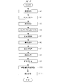
- FIG. FIG. 2 is a perspective view schematically showing the outline of the configuration of parts that constitute the ground electrode shown in FIG. 1; It is a flow explaining the formation process and washing
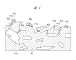
- 1 is an enlarged cross-sectional view showing the vicinity of the surface of a protective film for a plasma processing apparatus according to an embodiment of the present invention
- FIG. 4 is a graph showing the relationship between the elution rate and time in the process of cleaning the protective film for plasma processing equipment.
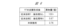
- 10 is a table showing the number of foreign matter when plasma etching is performed in each of the conventional techniques 1, 2 and the present embodiment.
- Plasma etching may be applied in the manufacturing process of electronic devices and the like.
- a processing chamber of a plasma processing apparatus used for plasma etching is arranged inside a vacuum vessel and is therefore made of metal such as aluminum or stainless steel. Since the inner wall of the processing chamber of the plasma processing apparatus is exposed to high-frequency plasma and etching gas during the etching process, the inner wall surface is protected by forming a film with excellent plasma resistance.
- a film made of yttrium oxide may be used as such a protective film.
- the generation of foreign matter in the processing chamber causes manufacturing defects due to adherence of foreign matter to the etching target, resulting in a decrease in yield. Therefore, it is important to suppress the generation of foreign matter in the processing chamber.
- the generation of foreign matter in the processing chamber is correlated with the crystal size and phase ratio of the inner wall material.
- the coating containing yttrium oxide as a material is formed using, for example, an atmospheric plasma spraying method.
- an atmospheric plasma spraying method raw material powder with a size of 10 to 60 ⁇ m is introduced into a plasma flame together with a carrier gas, and the raw material particles in a molten or semi-molten state are sprayed onto the substrate surface to form a film.
- the surface unevenness is large, or a large number of pores are formed inside the film, and particles entering these pores react with the film itself or other members, There is a problem that it causes consumption or corrosion.
- Atmospheric plasma spraying is a film forming method that entrains air during film formation and causes cracks due to rapid cooling. For this reason, the surface of the film contains surface irregularities and buried pores (voids) that cause these. In other words, the surface of the film has a portion with weaker adhesion than the surroundings.
- polishing treatment is performed for the purpose of reducing unevenness, buried pores may open and thin portions may occur, or the film material removed by polishing may reattach to the surface due to static electricity. . Therefore, the film has a surface condition in which initial contaminants are likely to occur due to these factors.
- the porosity and surface roughness of the film after the formation of the film or after the post-treatment are examined for the film on the surface of the member constituting the inner wall of the processing chamber.
- the characteristics of the film such as porosity, surface roughness (Ra to arithmetic mean roughness), crystallite size, phase ratio, etc. cannot be evaluated by comparing them with a predetermined allowable range.
- the inspection of the member concerned is limited to only the inspection of appearance.
- the desired characteristics and performance are obtained at the locations where the coating formed on the surface of the member constituting the inner wall is arranged. It is not clear whether it has or not. Therefore, it is difficult to improve the reliability of the cleaning process only by performing the above inspection.
- Another inspection method for checking the quality of post-processing is to cut out a part of the member inside the processing chamber and inspect it.
- this inspection method it is necessary to perform operations such as cleaning the part after cutting the part of the member to be inspected from the member. Therefore, the film on the portion to be inspected is not formed in the same process as that on other members of the same type.
- foreign matter may be generated on the surface of the film to be inspected during the cutting process, impairing the accuracy of the inspection.
- the above technology impairs the reliability and processing yield of the plasma processing apparatus, and also causes an increase in manufacturing costs.
- FIG. 1 is a vertical cross-sectional view schematically showing the outline of the configuration of a plasma processing apparatus according to an embodiment of the present invention.
- the plasma processing apparatus shown in the figure forms a plasma in a processing chamber inside a vacuum chamber, and a mask layer preformed on the surface of a sample such as a semiconductor wafer placed in the processing chamber and a film to be processed thereunder.
- a plasma etching apparatus for etching a film structure having a layer using plasma.
- a plasma processing apparatus 100 of the embodiment shown in FIG. 1 has a metallic vacuum vessel 1 having a partially cylindrical shape.
- the plasma processing apparatus 100 also has a generator for generating an electric field or a magnetic field for forming plasma in a decompressed space inside the vacuum vessel 1, which is disposed above the vacuum vessel 1. It has a plasma forming part that supplies the internal space.
- the plasma processing apparatus 100 has an exhaust section which is arranged below the vacuum vessel 1 and connected to the vacuum vessel 1 and has a vacuum pump for evacuating the space inside the vacuum vessel 1 to reduce the pressure.
- the vacuum container 1 is connected to a transfer container whose outer side wall is another vacuum container 1 and in which a wafer, which is a sample to be processed, is transferred in an inner transfer space in which the pressure is reduced.
- a side wall of the vacuum vessel 1 is provided with a gate through which a wafer is conveyed through the inside of the side wall.
- the transfer container is connected so that the space inside the vacuum container 1 and the space inside the transfer container can be communicated with each other.
- the vacuum vessel 1 has a processing chamber 7, which is a space in which a sample to be processed is placed and plasma is generated.
- the processing chamber 7 has a cylindrical discharge portion disposed in the upper portion thereof, in which a plasma 15 is formed. are placed.
- the stage 6 has a circular upper surface on which a wafer 4, which is a substrate to be processed, is placed.
- the stage 6 has therein a heater for heating the wafer 4 and a coolant passage through which a coolant for cooling flows.
- a pipeline for supplying helium (He) gas, which is a heat transfer gas, is provided between the rear surface and the rear surface.
- He helium
- a metal electrode is arranged inside the stage 6, and a high frequency power supply 14 is provided to supply high frequency power to the electrode for forming a potential on the wafer 4 during processing of the wafer 4 using the plasma 15. They are electrically connected via an impedance matching device 13 . Charged particles such as ions inside the wafer 4 are attracted to the surface of the wafer 4 by the potential difference between the bias potential formed on the wafer 4 by the high-frequency power and the plasma during the formation of the plasma 15, thereby promoting the etching process.
- the wafer 4 is placed on the tip of an arm of a transfer device (not shown) such as a robot arm arranged in a transfer space inside the transfer container, transferred to the processing chamber 7 , and then placed on the stage 6 . be done.
- the wafer 4 placed on the stage 6 is attracted and held on the upper surface of the dielectric film by an electrostatic force generated by applying a DC voltage to the electrodes for electrostatic attraction.
- a disk-shaped shower plate 2 and a window member 3 are mounted above the upper end of a cylindrical side wall member surrounding the discharge portion of the vacuum chamber 1 with a ring-shaped member interposed therebetween.
- the window member 3 constitutes the vacuum vessel 1 together with the side wall member 41 around the discharge section.
- a sealing member such as an O-ring is interposed between the lower surface of the outer peripheral edge of the window member 3, the upper surface of the upper end of the side wall member, and the ring-shaped member disposed therebetween to connect these members.
- the processing chamber 7 inside the vacuum vessel 1 and the atmosphere of atmospheric pressure outside are airtightly partitioned.
- the window member 3 is a disk-shaped member made of ceramics (quartz in the present embodiment) through which the electric field of the microwave for forming the plasma 15 is transmitted.
- a shower plate 2 provided with a plurality of through holes 9 in the center thereof is arranged with a gap 8 of a size therebetween.
- the shower plate 2 constitutes the ceiling surface facing the inside of the processing chamber 7, and a processing gas whose flow rate is adjusted to a predetermined value by gas flow control means (not shown) is introduced into the gap 8, and the gap 8 is filled. After being diffused inside, it is introduced into the processing chamber 7 from above through the through-hole.
- the processing gas is introduced into the gap 8 by opening a valve 51 arranged on the processing gas supply pipe 50 connected to the ring-shaped member.
- a passage through which the plasma 15 inside the processing chamber 7, the products generated during the processing of the wafer 4, and the particles of the processing gas are discharged. is provided.
- a circular opening of the passage inside the processing chamber 7 is arranged as an exhaust port at a position directly below the stage 6 arranged above so that the central axes can be considered to be the same when viewed from above.
- a turbo-molecular pump 12 Connected to the bottom surface of the vacuum vessel 1 are a turbo-molecular pump 12 that constitutes a vacuum pump for an exhaust section, and a dry pump 11 that is arranged downstream of the turbo-molecular pump 12 .
- the inlet of the turbo-molecular pump 12 is connected to the exhaust port by an exhaust pipe.
- a valve 18 is arranged on the exhaust pipe connecting the turbo-molecular pump 12 and the dry pump 11 , and the exhaust pipe between the valve 18 and the dry pump 11 is connected to the bottom surface of the vacuum vessel 1 .
- Another exhaust pipe 10 communicating with the bottom of the processing chamber 7 is connected.
- This other exhaust pipe 10 is branched into two pipe lines on the way and then connected so as to merge again into one, and valves 17 and 19 are arranged on each of the branched portions.
- the valve 17 is a slow evacuation valve for slowly evacuating the processing chamber 7 from atmospheric pressure to vacuum by the dry pump 11, and the valve 19 is for high-speed evacuation by the dry pump 11. This is the main exhaust valve for
- the processing chamber 7 is equipped with a pressure sensor 75 for detecting the internal pressure.
- a pressure sensor 75 for detecting the internal pressure.
- a disc-shaped pressure control plate 16 is arranged to adjust the flow rate or speed of the exhaust gas by increasing or decreasing the area.
- the pressure in the processing chamber 7 is increased or decreased by the flow rate or speed balance between the processing gas or other gas introduced into the processing chamber 7 through the gas inlet, which is a through hole of the shower plate 2, and the exhaust from the exhaust port. be.
- the pressure adjusting plate 16 is adjusted in vertical position. , the exhaust flow rate or speed is adjusted so that the pressure in the processing chamber 7 is realized according to the processing conditions.
- Plasma forming portions are arranged above and on the outer peripheral side of the metal side wall surrounding the outer circumference of the discharge portion of the processing chamber 7 in the upper portion of the vacuum vessel 1 and the window member 3 .
- the plasma forming section has a magnetron oscillator 20 for outputting an electric field of microwaves for forming the plasma 15 and a waveguide 21 for propagating the microwaves to the processing chamber 7 .
- the waveguide 21 has a rectangular portion extending in the horizontal direction (horizontal direction in the drawing) and having a rectangular or square cross section, and a cylindrical portion connected to one end of the rectangular portion and extending in the vertical direction.
- a magnetron oscillator 20 is arranged at the other end of the square portion.
- the lower end of the circular portion is connected to the upper end of a cylindrical cavity located above the window member 3 and having a diameter larger than the diameter of the circular portion and approximately the same size as the window member 3. ing. Furthermore, a ring-shaped magnetic field is supplied to the upper portion of the hollow portion, the outer peripheral side thereof, the outer peripheral side of the side wall of the vacuum vessel 1 surrounding the discharge portion, and the portion surrounding the discharge portion of the processing chamber 7, which is a means for generating a magnetic field by supplying DC power. solenoid coils 22, 23 are provided.
- the inner wall surface of the side wall member 41 of the processing chamber 7 is the surface exposed to the plasma 15 formed in the discharge section, and in order to stabilize the potential of the plasma 15, the processing chamber 7 has a component functioning as a ground.
- a ring-shaped ground electrode 40 functioning as a ground is arranged above the stage 6 so as to surround the upper surface of the stage 6 in the discharge section.
- the ground electrode 40 is configured using a metal member such as a stainless alloy or an aluminum alloy as a base material. Since the ground electrode 40 is exposed to the plasma 15, it interacts with highly reactive or corrosive particles in the plasma 15, and may become a source of corrosion, metal contamination, or foreign matter due to the produced products. is high.
- a coating 42 of material is disposed over the surface of the ground electrode 40 .
- the ground electrode 40 can suppress damage such as corrosion of the ground electrode 40 due to plasma while maintaining the function as a ground.
- the film 42 may be a laminated film.
- the side wall member 41 surrounding the discharge portion of the vacuum vessel 1 of the present embodiment is made of a base material made of metal such as stainless alloy or aluminum alloy, but does not function as a ground.
- the inner surface of the side wall member 41 is subjected to surface treatment such as passivation, thermal spraying, PVD, or CVD. It has been subjected.
- the following ceramic parts may be formed.
- a ring-shaped or cylindrical part made of ceramic such as yttrium oxide or quartz is provided on the inner side wall surface. may be arranged so as to cover the inner wall surface with respect to the plasma 15 along the .
- the part between the side wall member 41 and the plasma 15 inhibits the contact between the side wall member 41 and the plasma 15 and suppresses the consumption of the side wall member 41 surface-treated by the plasma 15 .
- FIG. 2 is a perspective view schematically showing the outline of the configuration of the parts that constitute the ground electrode shown in FIG.
- FIG. 2 shows a view of the ring-shaped or cylindrical ground electrode 40 shown in FIG.
- the ground electrode 40 has a cylindrical shape with a predetermined thickness as a whole, and has an inner side wall and an outer side wall each having the same inner diameter around the central axis in the vertical direction. . Further, the ground electrode 40 has a cylindrical main side wall portion and a ring-shaped electrode portion disposed further upward from the upper end of the main side wall portion. The location is smaller than the lower major sidewall portion. A rectangular opening 43 of a through-hole that constitutes a gate 49 is arranged in the middle portion in the vertical direction of the cylindrical main side wall portion.
- the ground electrode 40 With the ground electrode 40 attached inside the processing chamber 7 , the ground electrode 40 is arranged between the inner side wall and the processing chamber 7 .
- the ground electrode 40 has a lower portion covering the inner wall surface of the side wall member 41 of the vacuum chamber 1 surrounding the stage 6 on the outer peripheral side of the stage 6 against the plasma 15, and an upper portion disposed inside the side wall member 41 surrounding the discharge portion. It has a vertical length sufficient to cover the inner wall surface of the side wall member 41 against the plasma 15 . This shape protects the sidewall member 41 from plasma 15 interaction.
- a step of forming a plasma-resistant film for protecting a ground electrode for a plasma processing apparatus (conventional technique 1), a first post-treatment (conventional technique 2) performed after the formation of the film, and a second It shows a procedure for performing post-processing (an example of the present embodiment).
- a ground electrode is prepared and the surface of the ground electrode is degreased (step S1).
- the ground electrode prepared and degreased here is a single electrode before being incorporated into the plasma processing apparatus 100 of FIG.
- step S2 the surface of the ground electrode is sandblasted as a pretreatment for film formation.
- an abrasive particles
- step S3 the surface of the ground electrode is degreased.
- a film is formed on the surface of the ground electrode by atmospheric plasma spraying (APS) (step S4).
- APS atmospheric plasma spraying
- a film made of YF 3 (yttrium fluoride) is formed.
- YOF yttrium oxofluoride
- Y 2 O 3 oxo yttrium
- YAG yttrium aluminum garnet
- Atmospheric plasma spraying is a method of forming a coating on the surface of an object by thermal spraying in an atmosphere of atmospheric pressure. It is sprayed on the surface of the object and laminated to form a film.
- the processes of steps S1 to S4 up to this point are referred to as prior art 1.
- step S5 the ground electrode with the film formed thereon is immersed in pure water and subjected to ultrasonic cleaning
- step S6 the ground electrode is treated with a chemical solution
- step S7 the ground electrode is again immersed in pure water and subjected to ultrasonic cleaning
- step S8 the ground electrode is polished (step S8), and then the ground electrode is again immersed in pure water and subjected to ultrasonic cleaning (step S9).
- the process (first post-processing) of steps S5 to S9 up to this point is referred to as prior art 2.
- step S10 the ground electrode with the coating is immersed in dilute nitric acid and subjected to ultrasonic irradiation (step S10).
- step S11 the ground electrode is washed with pure water (step S11).
- the steps S10 and S11 (second post-processing) up to this point are an example of the present embodiment.
- the film formation and the post-treatments are completed.
- the ground electrode 40 is incorporated into the plasma processing apparatus 100 shown in FIG.
- step S10 in addition to the conventional film formation steps (steps S1 to S4) and first post-treatment (steps S5 to S9), ultrasonic cleaning in dilute nitric acid (step S10) will be described below.
- the main feature is that it is performed under conditions that In other words, the main feature of this embodiment is that a portion weakly bonded to the surroundings is removed by acid dissolution and ultrasonic vibration by cleaning in which ultrasonic waves are applied in dilute nitric acid.
- the surface of the film 42 is in a state of having irregularities, pores, and surface-adhering foreign matter.
- the surface-adhering foreign matter includes a water-adsorbed substance 43 a that is adsorbed by water on the surface of the film 42 and between the film 42 and the film 42 .
- the surface-adhering foreign matter includes an electrostatically attracted matter 43b that is electrostatically attracted to the surface of the film 42.
- the surface-adhering foreign matter there is a stress-fixed substance 43c that is stress-fixed by the unevenness of the surface of the film 42.
- FIG. Many of these surface-adhering foreign substances are foreign substances separated from the film 42 in the polishing step of the first post-treatment or the like, and their materials are the same as the materials of the film 42 .
- the narrow portion 42a is a part of the film 42, but is a portion having a small thickness and thus weakly bonded to the surroundings. Surface contaminants are generated by breaking or dissolving the narrow portion 42a.
- the ultrasonic cleaning (step S10) in the dilute nitric acid of the present embodiment removes these surface-adhered foreign matter and the narrow portion 42a, resulting in the generation of foreign matter due to the surface state of the film after the post-treatment. to prevent
- Fig. 5 shows the dilute nitric acid ultrasonic cleaning time and yttrium elution rate.
- the elution rate referred to here is the elution amount (weight) of yttrium eluted per unit time from the measurement point (marker) before the relevant time to the relevant time.
- the example of the present embodiment is a graph consisting of plots of black squares, and the graph will be described here.
- Each graph shown in FIG. 5 is obtained by averaging a plurality of plots for each predetermined time.
- the elution rate of yttrium greatly decreases.
- the water adsorbate 43a and the electrostatically adsorbate 43b shown in FIG. 4 are eluted and separated from the surface of the film 42, and the removal of these substances greatly reduces the elution rate of yttrium. .
- the elution rate of yttrium which had decreased, once increased and then decreased.
- the remaining electrostatically attracted objects 43b and the stress-fixed objects 43c shown in FIG. 4 are eluted and separated.
- the pinched portion 42a is eluted, and along with this, the tip portion connected to the pinched portion 42a is separated from the film 42 and eluted. Therefore, in the second phase 1B, the elution rate of yttrium, which had decreased, increases once. After that, the elution rate decreases due to the decrease due to the elution of the foreign matter adhering to the surface and the elution of the pinched portion 42a.
- the elution rate of yttrium greatly increases from about 60 minutes after the start of dilute nitric acid ultrasonic cleaning, entering the third phase 1C.
- the elution rate of yttrium increases by 1.5 times or more compared to immediately before. This is because the thin portion 42b shown in FIG. 4 dissolves and the pores 42c are released, thereby increasing the surface area of the film 42.
- the pure water cleaning in step S11 is performed, and the ground electrode installed in the plasma processing apparatus is in a state where foreign matter is likely to be released from the film 42 .
- the dilute nitric acid ultrasonic cleaning should be stopped before the elution rate starts to increase in the third aspect 1C.
- the ground electrode to be cleaned is immersed in a diluted nitric acid solution, and ultrasonic irradiation is started to increase the elution rate of yttrium. Washing is stopped after the (elution amount) decreases (first phase 1A), increases again, decreases again (second phase 1B), and then increases again (third phase 1C).
- the cleaning step the elution rate of yttrium is detected during cleaning, and the elution rate of yttrium after the start of ultrasonic irradiation undergoes a first decrease, a first increase, and a second decrease in order. and stop washing before the second increase occurs.
- cleaning is stopped 10 minutes or 20 minutes after the start of ultrasonic irradiation and before 60 minutes have passed.
- the source of foreign matter on the surface of the inner wall material generated in the post-treatment after film formation can be removed, and the post-treatment can be completed in a state in which the exposure of the pores 42c is suppressed. That is, since the surface area of the film 42 can be prevented from increasing excessively, it is possible to suppress the generation of foreign substances due to the surface condition of the film 42 after the ground electrode is installed in the plasma processing apparatus. As a result, it is possible to improve the reliability of the method for cleaning the protective film for the plasma processing apparatus.
- elution rate elution amount
- these elution rates serve as criteria for determining whether or not cleaning is completed at the desired timing, or when it is time to terminate cleaning.
- the quality of the film 42 can be managed.
- the concentration of dilute nitric acid used in the dilute nitric acid ultrasonic cleaning described above will be explained.
- FIG. 5 an example of this embodiment is indicated by the black square plot.
- the concentration of dilute nitric acid is set to an intermediate level (0.001 mol/liter or more and 0.05 mol/liter or less).
- a graph composed of plotted black circles is a graph of a comparative example in which the concentration of dilute nitric acid was set higher than 0.05 mol/liter.
- a graph composed of black triangle plots is a graph of a comparative example in which the concentration of dilute nitric acid is set lower than 0.001 mol/liter.
- a graph of white circles is a graph of a comparative example in which an object is immersed in pure water instead of dilute nitric acid and subjected to ultrasonic cleaning.
- the dilute nitric acid ultrasonic cleaning of the present embodiment in which cleaning is stopped after the initial increase in the elution rate and before the elution rate increases again. Therefore, in order to separate the first phase 1A and the second phase 1B, the dilute nitric acid concentration must be 0.05 mol/liter or less.
- the increase in the third aspect 1C occurs before the increase in the dissolution rate confirmed in the second aspect 1B of the example of the present embodiment occurs. That is, the third phase 1C (irradiation upper limit) is reached only by physical destruction by ultrasonic waves. For this reason, it is difficult to perform the dilute nitric acid ultrasonic cleaning of the present embodiment in which the cleaning is stopped after the initial increase in the elution rate and before the elution rate increases again. Furthermore, since the narrow portion 42a and the stress fixing object 43c in the second phase 1B cannot be removed, sufficient cleaning cannot be performed. Therefore, the diluted nitric acid concentration should be 0.001 mol/liter or more.
- the table in FIG. 6 shows the results of the experiments conducted by the present inventors.
- the table of FIG. 6 shows the number of foreign substances falling on the wafer surface when plasma etching is performed using the plasma processing apparatus 100 shown in FIG.
- prior art 1 no post-treatment
- the foreign matter amount was 5.67.
- the present invention can be widely used in cleaning methods for protective films for plasma processing equipment.
Landscapes
- Physics & Mathematics (AREA)
- Engineering & Computer Science (AREA)
- Plasma & Fusion (AREA)
- Chemical & Material Sciences (AREA)
- Analytical Chemistry (AREA)
- Health & Medical Sciences (AREA)
- Epidemiology (AREA)
- Public Health (AREA)
- Drying Of Semiconductors (AREA)
- Chemical Vapour Deposition (AREA)
- Cleaning Or Drying Semiconductors (AREA)
Priority Applications (6)
| Application Number | Priority Date | Filing Date | Title |
|---|---|---|---|
| PCT/JP2021/030850 WO2023026331A1 (ja) | 2021-08-23 | 2021-08-23 | プラズマ処理装置用保護皮膜の洗浄方法 |
| KR1020227029775A KR102709625B1 (ko) | 2021-08-23 | 2021-08-23 | 플라스마 처리 장치용 보호 피막의 세정 방법 |
| CN202180017270.1A CN116018669B (zh) | 2021-08-23 | 2021-08-23 | 等离子处理装置用保护皮膜的清洗方法 |
| JP2022551293A JP7358655B2 (ja) | 2021-08-23 | 2021-08-23 | プラズマ処理装置用保護皮膜の洗浄方法 |
| US17/802,639 US12437978B2 (en) | 2021-08-23 | 2021-08-23 | Cleaning method of film layer in the plasma processing apparatus |
| TW111129529A TWI849469B (zh) | 2021-08-23 | 2022-08-05 | 電漿處理裝置用保護皮膜之洗淨方法 |
Applications Claiming Priority (1)
| Application Number | Priority Date | Filing Date | Title |
|---|---|---|---|
| PCT/JP2021/030850 WO2023026331A1 (ja) | 2021-08-23 | 2021-08-23 | プラズマ処理装置用保護皮膜の洗浄方法 |
Publications (1)
| Publication Number | Publication Date |
|---|---|
| WO2023026331A1 true WO2023026331A1 (ja) | 2023-03-02 |
Family
ID=85321630
Family Applications (1)
| Application Number | Title | Priority Date | Filing Date |
|---|---|---|---|
| PCT/JP2021/030850 Ceased WO2023026331A1 (ja) | 2021-08-23 | 2021-08-23 | プラズマ処理装置用保護皮膜の洗浄方法 |
Country Status (6)
| Country | Link |
|---|---|
| US (1) | US12437978B2 (https=) |
| JP (1) | JP7358655B2 (https=) |
| KR (1) | KR102709625B1 (https=) |
| CN (1) | CN116018669B (https=) |
| TW (1) | TWI849469B (https=) |
| WO (1) | WO2023026331A1 (https=) |
Families Citing this family (1)
| Publication number | Priority date | Publication date | Assignee | Title |
|---|---|---|---|---|
| KR102914217B1 (ko) | 2024-07-11 | 2026-01-20 | (주)위지트 | 플라즈마 보호 피막 세정 방법 |
Citations (4)
| Publication number | Priority date | Publication date | Assignee | Title |
|---|---|---|---|---|
| WO2007007782A1 (ja) * | 2005-07-14 | 2007-01-18 | Tohoku University | 多層構造体及びその洗浄方法 |
| JP2009174000A (ja) * | 2008-01-24 | 2009-08-06 | Shin Etsu Chem Co Ltd | セラミックス溶射部材及びその製造方法ならびにセラミックス溶射部材用研磨メディア |
| JP2017031457A (ja) * | 2015-07-31 | 2017-02-09 | 信越化学工業株式会社 | イットリウム系溶射皮膜、及びその製造方法 |
| JP2019519091A (ja) * | 2016-04-01 | 2019-07-04 | アプライド マテリアルズ インコーポレイテッドApplied Materials,Incorporated | オキシフッ化物を沈殿させるクリーニングプロセス |
Family Cites Families (8)
| Publication number | Priority date | Publication date | Assignee | Title |
|---|---|---|---|---|
| JP2009176787A (ja) | 2008-01-22 | 2009-08-06 | Hitachi High-Technologies Corp | エッチング処理装置及びエッチング処理室用部材 |
| JP5530794B2 (ja) * | 2010-04-28 | 2014-06-25 | 株式会社日立ハイテクノロジーズ | 真空処理装置及びプラズマ処理方法 |
| JP2012222225A (ja) * | 2011-04-12 | 2012-11-12 | Hitachi High-Technologies Corp | プラズマ処理装置 |
| JP5750496B2 (ja) * | 2013-12-11 | 2015-07-22 | 株式会社日立ハイテクノロジーズ | プラズマ処理方法 |
| TWM563652U (zh) | 2016-10-13 | 2018-07-11 | 美商應用材料股份有限公司 | 用於電漿處理裝置的腔室部件及包含其之裝置 |
| JP7122854B2 (ja) * | 2018-04-20 | 2022-08-22 | 株式会社日立ハイテク | プラズマ処理装置およびプラズマ処理装置用部材、またはプラズマ処理装置の製造方法およびプラズマ処理装置用部材の製造方法 |
| WO2020100227A1 (ja) * | 2018-11-14 | 2020-05-22 | 株式会社日立ハイテクノロジーズ | プラズマ処理装置及びそれを用いた被処理試料の処理方法 |
| JP7324290B2 (ja) | 2019-09-09 | 2023-08-09 | 富士フイルム株式会社 | 処理液、キット、処理液の製造方法、基板の洗浄方法、基板の処理方法 |
-
2021
- 2021-08-23 JP JP2022551293A patent/JP7358655B2/ja active Active
- 2021-08-23 CN CN202180017270.1A patent/CN116018669B/zh active Active
- 2021-08-23 US US17/802,639 patent/US12437978B2/en active Active
- 2021-08-23 WO PCT/JP2021/030850 patent/WO2023026331A1/ja not_active Ceased
- 2021-08-23 KR KR1020227029775A patent/KR102709625B1/ko active Active
-
2022
- 2022-08-05 TW TW111129529A patent/TWI849469B/zh active
Patent Citations (4)
| Publication number | Priority date | Publication date | Assignee | Title |
|---|---|---|---|---|
| WO2007007782A1 (ja) * | 2005-07-14 | 2007-01-18 | Tohoku University | 多層構造体及びその洗浄方法 |
| JP2009174000A (ja) * | 2008-01-24 | 2009-08-06 | Shin Etsu Chem Co Ltd | セラミックス溶射部材及びその製造方法ならびにセラミックス溶射部材用研磨メディア |
| JP2017031457A (ja) * | 2015-07-31 | 2017-02-09 | 信越化学工業株式会社 | イットリウム系溶射皮膜、及びその製造方法 |
| JP2019519091A (ja) * | 2016-04-01 | 2019-07-04 | アプライド マテリアルズ インコーポレイテッドApplied Materials,Incorporated | オキシフッ化物を沈殿させるクリーニングプロセス |
Also Published As
| Publication number | Publication date |
|---|---|
| JP7358655B2 (ja) | 2023-10-10 |
| KR102709625B1 (ko) | 2024-09-26 |
| JPWO2023026331A1 (https=) | 2023-03-02 |
| TWI849469B (zh) | 2024-07-21 |
| CN116018669B (zh) | 2025-09-19 |
| KR20230031187A (ko) | 2023-03-07 |
| CN116018669A (zh) | 2023-04-25 |
| US20240203708A1 (en) | 2024-06-20 |
| TW202309976A (zh) | 2023-03-01 |
| US12437978B2 (en) | 2025-10-07 |
Similar Documents
| Publication | Publication Date | Title |
|---|---|---|
| TWI778245B (zh) | 電漿處理裝置及電漿處理裝置用構件、和電漿處理裝置之製造方法及電漿處理裝置用構件之製造方法 | |
| CN100386467C (zh) | 等离子体处理容器的再生方法、等离子体处理容器内部部件、等离子体处理容器内部部件的制造方法以及等离子体处理装置 | |
| JP2018107313A (ja) | ガス供給装置、プラズマ処理装置及びガス供給装置の製造方法 | |
| JP4856978B2 (ja) | プラズマエッチング装置及び処理室の内壁の形成方法 | |
| US20080314321A1 (en) | Plasma processing apparatus | |
| TWI816448B (zh) | 內壁構件的再生方法 | |
| JP7358655B2 (ja) | プラズマ処理装置用保護皮膜の洗浄方法 | |
| JP4181069B2 (ja) | プラズマ処理装置 | |
| JP4098259B2 (ja) | プラズマ処理装置 | |
| CN115836378B (zh) | 用于氢与氨等离子体应用的具有保护性陶瓷涂层的处理套件 | |
| JP2015141956A (ja) | プラズマ処理装置およびプラズマ処理方法 | |
| TWI830599B (zh) | 內壁構件的再生方法 | |
| JP2008098660A (ja) | プラズマ処理装置 | |
| JP7519893B2 (ja) | シャワーヘッドの製造方法およびシャワーヘッド、ならびにプラズマ処理装置 | |
| JP2004296753A (ja) | プラズマ露出部品及びその表面処理方法並びにプラズマ処理装置 |
Legal Events
| Date | Code | Title | Description |
|---|---|---|---|
| ENP | Entry into the national phase |
Ref document number: 2022551293 Country of ref document: JP Kind code of ref document: A |
|
| WWE | Wipo information: entry into national phase |
Ref document number: 17802639 Country of ref document: US |
|
| 121 | Ep: the epo has been informed by wipo that ep was designated in this application |
Ref document number: 21954948 Country of ref document: EP Kind code of ref document: A1 |
|
| NENP | Non-entry into the national phase |
Ref country code: DE |
|
| 122 | Ep: pct application non-entry in european phase |
Ref document number: 21954948 Country of ref document: EP Kind code of ref document: A1 |
|
| WWG | Wipo information: grant in national office |
Ref document number: 202180017270.1 Country of ref document: CN |
|
| WWG | Wipo information: grant in national office |
Ref document number: 17802639 Country of ref document: US |