WO2023026331A1 - プラズマ処理装置用保護皮膜の洗浄方法 - Google Patents
プラズマ処理装置用保護皮膜の洗浄方法 Download PDFInfo
- Publication number
- WO2023026331A1 WO2023026331A1 PCT/JP2021/030850 JP2021030850W WO2023026331A1 WO 2023026331 A1 WO2023026331 A1 WO 2023026331A1 JP 2021030850 W JP2021030850 W JP 2021030850W WO 2023026331 A1 WO2023026331 A1 WO 2023026331A1
- Authority
- WO
- WIPO (PCT)
- Prior art keywords
- cleaning
- plasma
- processing apparatus
- plasma processing
- film
- Prior art date
Links
- 238000000034 method Methods 0.000 title claims abstract description 56
- 238000005406 washing Methods 0.000 title abstract description 8
- 238000009832 plasma treatment Methods 0.000 title abstract 4
- 229910017604 nitric acid Inorganic materials 0.000 claims abstract description 39
- GRYLNZFGIOXLOG-UHFFFAOYSA-N Nitric acid Chemical compound O[N+]([O-])=O GRYLNZFGIOXLOG-UHFFFAOYSA-N 0.000 claims abstract description 38
- 229910052727 yttrium Inorganic materials 0.000 claims abstract description 23
- 239000000463 material Substances 0.000 claims abstract description 22
- VWQVUPCCIRVNHF-UHFFFAOYSA-N yttrium atom Chemical compound [Y] VWQVUPCCIRVNHF-UHFFFAOYSA-N 0.000 claims abstract description 22
- 230000007423 decrease Effects 0.000 claims abstract description 16
- 230000001678 irradiating effect Effects 0.000 claims abstract description 4
- 238000012545 processing Methods 0.000 claims description 101
- 238000004140 cleaning Methods 0.000 claims description 51
- 238000010828 elution Methods 0.000 claims description 32
- 230000001681 protective effect Effects 0.000 claims description 23
- 239000000758 substrate Substances 0.000 claims description 6
- 239000011253 protective coating Substances 0.000 claims description 4
- 238000011282 treatment Methods 0.000 abstract description 31
- 238000004090 dissolution Methods 0.000 abstract description 5
- 238000002604 ultrasonography Methods 0.000 abstract 2
- 239000010408 film Substances 0.000 description 79
- 238000004506 ultrasonic cleaning Methods 0.000 description 21
- 239000007789 gas Substances 0.000 description 14
- 238000007689 inspection Methods 0.000 description 14
- 239000011148 porous material Substances 0.000 description 13
- 239000011248 coating agent Substances 0.000 description 12
- 238000000576 coating method Methods 0.000 description 12
- 230000008569 process Effects 0.000 description 12
- 230000015572 biosynthetic process Effects 0.000 description 11
- XLYOFNOQVPJJNP-UHFFFAOYSA-N water Substances O XLYOFNOQVPJJNP-UHFFFAOYSA-N 0.000 description 10
- 238000001020 plasma etching Methods 0.000 description 9
- 239000000126 substance Substances 0.000 description 9
- 238000005530 etching Methods 0.000 description 8
- 238000012546 transfer Methods 0.000 description 8
- 229910052751 metal Inorganic materials 0.000 description 7
- 239000002184 metal Substances 0.000 description 7
- 238000012805 post-processing Methods 0.000 description 7
- 239000002245 particle Substances 0.000 description 6
- 238000007750 plasma spraying Methods 0.000 description 6
- 230000003247 decreasing effect Effects 0.000 description 5
- 238000004519 manufacturing process Methods 0.000 description 5
- 230000002093 peripheral effect Effects 0.000 description 5
- 238000005498 polishing Methods 0.000 description 5
- 230000003746 surface roughness Effects 0.000 description 5
- 230000007797 corrosion Effects 0.000 description 4
- 238000005260 corrosion Methods 0.000 description 4
- JNDMLEXHDPKVFC-UHFFFAOYSA-N aluminum;oxygen(2-);yttrium(3+) Chemical compound [O-2].[O-2].[O-2].[Al+3].[Y+3] JNDMLEXHDPKVFC-UHFFFAOYSA-N 0.000 description 3
- 239000000919 ceramic Substances 0.000 description 3
- 230000000052 comparative effect Effects 0.000 description 3
- 238000007796 conventional method Methods 0.000 description 3
- 238000005520 cutting process Methods 0.000 description 3
- 230000006378 damage Effects 0.000 description 3
- 230000005684 electric field Effects 0.000 description 3
- 230000006870 function Effects 0.000 description 3
- 230000006872 improvement Effects 0.000 description 3
- SIWVEOZUMHYXCS-UHFFFAOYSA-N oxo(oxoyttriooxy)yttrium Chemical compound O=[Y]O[Y]=O SIWVEOZUMHYXCS-UHFFFAOYSA-N 0.000 description 3
- 238000007751 thermal spraying Methods 0.000 description 3
- 229910019901 yttrium aluminum garnet Inorganic materials 0.000 description 3
- 229910000838 Al alloy Inorganic materials 0.000 description 2
- 239000002156 adsorbate Substances 0.000 description 2
- 229910045601 alloy Inorganic materials 0.000 description 2
- 239000000956 alloy Substances 0.000 description 2
- 239000000356 contaminant Substances 0.000 description 2
- 238000011109 contamination Methods 0.000 description 2
- 239000002826 coolant Substances 0.000 description 2
- 238000001816 cooling Methods 0.000 description 2
- 239000010453 quartz Substances 0.000 description 2
- 239000002994 raw material Substances 0.000 description 2
- VYPSYNLAJGMNEJ-UHFFFAOYSA-N silicon dioxide Inorganic materials O=[Si]=O VYPSYNLAJGMNEJ-UHFFFAOYSA-N 0.000 description 2
- 238000001179 sorption measurement Methods 0.000 description 2
- 238000005507 spraying Methods 0.000 description 2
- 229910018072 Al 2 O 3 Inorganic materials 0.000 description 1
- 238000012935 Averaging Methods 0.000 description 1
- CHBIYWIUHAZZNR-UHFFFAOYSA-N [Y].FOF Chemical compound [Y].FOF CHBIYWIUHAZZNR-UHFFFAOYSA-N 0.000 description 1
- 239000002253 acid Substances 0.000 description 1
- 229910052782 aluminium Inorganic materials 0.000 description 1
- XAGFODPZIPBFFR-UHFFFAOYSA-N aluminium Chemical compound [Al] XAGFODPZIPBFFR-UHFFFAOYSA-N 0.000 description 1
- 238000005513 bias potential Methods 0.000 description 1
- 239000012159 carrier gas Substances 0.000 description 1
- 230000002596 correlated effect Effects 0.000 description 1
- 239000013078 crystal Substances 0.000 description 1
- 230000007547 defect Effects 0.000 description 1
- 230000005611 electricity Effects 0.000 description 1
- 238000005516 engineering process Methods 0.000 description 1
- 238000002474 experimental method Methods 0.000 description 1
- 238000010438 heat treatment Methods 0.000 description 1
- 239000001307 helium Substances 0.000 description 1
- 229910052734 helium Inorganic materials 0.000 description 1
- SWQJXJOGLNCZEY-UHFFFAOYSA-N helium atom Chemical compound [He] SWQJXJOGLNCZEY-UHFFFAOYSA-N 0.000 description 1
- 230000003993 interaction Effects 0.000 description 1
- 150000002500 ions Chemical class 0.000 description 1
- 239000003550 marker Substances 0.000 description 1
- 238000005259 measurement Methods 0.000 description 1
- 230000015654 memory Effects 0.000 description 1
- 238000012986 modification Methods 0.000 description 1
- 230000004048 modification Effects 0.000 description 1
- 150000007524 organic acids Chemical class 0.000 description 1
- -1 oxo yttrium Chemical compound 0.000 description 1
- 238000002161 passivation Methods 0.000 description 1
- 238000005240 physical vapour deposition Methods 0.000 description 1
- 239000000843 powder Substances 0.000 description 1
- 238000003672 processing method Methods 0.000 description 1
- 230000001737 promoting effect Effects 0.000 description 1
- 230000001902 propagating effect Effects 0.000 description 1
- 238000007789 sealing Methods 0.000 description 1
- 239000004065 semiconductor Substances 0.000 description 1
- 239000010935 stainless steel Substances 0.000 description 1
- 229910001220 stainless steel Inorganic materials 0.000 description 1
- 230000003068 static effect Effects 0.000 description 1
- 238000004381 surface treatment Methods 0.000 description 1
- 239000010409 thin film Substances 0.000 description 1
- 229940105963 yttrium fluoride Drugs 0.000 description 1
- RBORBHYCVONNJH-UHFFFAOYSA-K yttrium(iii) fluoride Chemical compound F[Y](F)F RBORBHYCVONNJH-UHFFFAOYSA-K 0.000 description 1
Images


Classifications
-
- H—ELECTRICITY
- H01—ELECTRIC ELEMENTS
- H01J—ELECTRIC DISCHARGE TUBES OR DISCHARGE LAMPS
- H01J37/00—Discharge tubes with provision for introducing objects or material to be exposed to the discharge, e.g. for the purpose of examination or processing thereof
- H01J37/32—Gas-filled discharge tubes
- H01J37/32431—Constructional details of the reactor
- H01J37/32798—Further details of plasma apparatus not provided for in groups H01J37/3244 - H01J37/32788; special provisions for cleaning or maintenance of the apparatus
- H01J37/32853—Hygiene
- H01J37/32862—In situ cleaning of vessels and/or internal parts
-
- B—PERFORMING OPERATIONS; TRANSPORTING
- B08—CLEANING
- B08B—CLEANING IN GENERAL; PREVENTION OF FOULING IN GENERAL
- B08B3/00—Cleaning by methods involving the use or presence of liquid or steam
- B08B3/04—Cleaning involving contact with liquid
- B08B3/10—Cleaning involving contact with liquid with additional treatment of the liquid or of the object being cleaned, e.g. by heat, by electricity or by vibration
- B08B3/12—Cleaning involving contact with liquid with additional treatment of the liquid or of the object being cleaned, e.g. by heat, by electricity or by vibration by sonic or ultrasonic vibrations
-
- H—ELECTRICITY
- H01—ELECTRIC ELEMENTS
- H01J—ELECTRIC DISCHARGE TUBES OR DISCHARGE LAMPS
- H01J37/00—Discharge tubes with provision for introducing objects or material to be exposed to the discharge, e.g. for the purpose of examination or processing thereof
- H01J37/32—Gas-filled discharge tubes
- H01J37/32431—Constructional details of the reactor
- H01J37/32458—Vessel
- H01J37/32477—Vessel characterised by the means for protecting vessels or internal parts, e.g. coatings
- H01J37/32495—Means for protecting the vessel against plasma
-
- H—ELECTRICITY
- H01—ELECTRIC ELEMENTS
- H01L—SEMICONDUCTOR DEVICES NOT COVERED BY CLASS H10
- H01L21/00—Processes or apparatus adapted for the manufacture or treatment of semiconductor or solid state devices or of parts thereof
- H01L21/02—Manufacture or treatment of semiconductor devices or of parts thereof
- H01L21/04—Manufacture or treatment of semiconductor devices or of parts thereof the devices having potential barriers, e.g. a PN junction, depletion layer or carrier concentration layer
- H01L21/18—Manufacture or treatment of semiconductor devices or of parts thereof the devices having potential barriers, e.g. a PN junction, depletion layer or carrier concentration layer the devices having semiconductor bodies comprising elements of Group IV of the Periodic Table or AIIIBV compounds with or without impurities, e.g. doping materials
- H01L21/30—Treatment of semiconductor bodies using processes or apparatus not provided for in groups H01L21/20 - H01L21/26
- H01L21/302—Treatment of semiconductor bodies using processes or apparatus not provided for in groups H01L21/20 - H01L21/26 to change their surface-physical characteristics or shape, e.g. etching, polishing, cutting
- H01L21/306—Chemical or electrical treatment, e.g. electrolytic etching
- H01L21/3065—Plasma etching; Reactive-ion etching
-
- H—ELECTRICITY
- H01—ELECTRIC ELEMENTS
- H01J—ELECTRIC DISCHARGE TUBES OR DISCHARGE LAMPS
- H01J2237/00—Discharge tubes exposing object to beam, e.g. for analysis treatment, etching, imaging
- H01J2237/32—Processing objects by plasma generation
- H01J2237/33—Processing objects by plasma generation characterised by the type of processing
- H01J2237/334—Etching
Definitions
- the present invention relates to a method for cleaning protective coatings for plasma processing equipment.
- Plasma etching is applied for microfabrication in the manufacture of electronic devices and magnetic memories. Since the inner wall of the processing chamber of a plasma processing apparatus that performs plasma etching is exposed to high-frequency plasma and etching gas during the etching process, the inner wall surface is protected by forming a film having excellent plasma resistance.
- Patent Document 1 Japanese Patent Application Laid-Open No. 2009-176787 discloses that a film material for the ground portion of a plasma etching apparatus is Al 2 O 3 , YAG, Y 2 O 3 , Gd 2 O 3 , Yb 2 O 3 or YF 3. It is described that any one type or two or more types are used. Further, Patent Document 2 (Japanese Patent Application Laid-Open No. 2017-31457) describes a cleaning method in which a base material having a thermal spray coating formed on the surface thereof is immersed in an organic acid.
- the plasma-resistant film is required to keep the surface roughness (Ra) and porosity low
- post-treatment such as polishing the surface is performed after the film is formed.
- foreign matter adhered to the surface is released due to the thin region or the inner wall material that is electrostatically attracted, and the foreign matter tends to adhere to the etching target. Therefore, there is a need for a cleaning method that reduces the generation of foreign matter after post-processing.
- An object of the present invention is to provide a method for cleaning a highly reliable protective film for a plasma processing apparatus.
- a method for cleaning a protective film for a plasma processing apparatus is a plasma processing method in which a wafer to be processed placed in a processing chamber arranged inside a vacuum vessel is processed using plasma generated in the processing chamber.
- a method for cleaning a protective film for a plasma processing apparatus which is formed on the surface of a substrate placed inside a processing chamber of a processing apparatus and contains a plasma-resistant material, comprising: (a) providing a film containing yttrium on the surface; (b) immersing the substrate in a dilute nitric acid solution and irradiating the film with ultrasonic waves for cleaning; After the elution rate of yttrium from the start of ultrasonic irradiation has undergone a first decrease, a first increase, and a second decrease in order, and before the second increase occurs, cleaning is performed. It should stop.
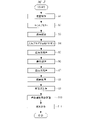
- FIG. 1 is a longitudinal sectional view schematically showing the outline of the configuration of a plasma processing apparatus according to an embodiment of the present invention
- FIG. FIG. 2 is a perspective view schematically showing the outline of the configuration of parts that constitute the ground electrode shown in FIG. 1; It is a flow explaining the formation process and washing
- 1 is an enlarged cross-sectional view showing the vicinity of the surface of a protective film for a plasma processing apparatus according to an embodiment of the present invention
- FIG. 4 is a graph showing the relationship between the elution rate and time in the process of cleaning the protective film for plasma processing equipment.
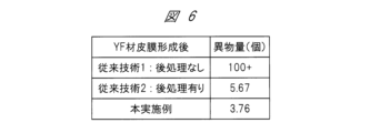
- 10 is a table showing the number of foreign matter when plasma etching is performed in each of the conventional techniques 1, 2 and the present embodiment.
- Plasma etching may be applied in the manufacturing process of electronic devices and the like.
- a processing chamber of a plasma processing apparatus used for plasma etching is arranged inside a vacuum vessel and is therefore made of metal such as aluminum or stainless steel. Since the inner wall of the processing chamber of the plasma processing apparatus is exposed to high-frequency plasma and etching gas during the etching process, the inner wall surface is protected by forming a film with excellent plasma resistance.
- a film made of yttrium oxide may be used as such a protective film.
- the generation of foreign matter in the processing chamber causes manufacturing defects due to adherence of foreign matter to the etching target, resulting in a decrease in yield. Therefore, it is important to suppress the generation of foreign matter in the processing chamber.
- the generation of foreign matter in the processing chamber is correlated with the crystal size and phase ratio of the inner wall material.
- the coating containing yttrium oxide as a material is formed using, for example, an atmospheric plasma spraying method.
- an atmospheric plasma spraying method raw material powder with a size of 10 to 60 ⁇ m is introduced into a plasma flame together with a carrier gas, and the raw material particles in a molten or semi-molten state are sprayed onto the substrate surface to form a film.
- the surface unevenness is large, or a large number of pores are formed inside the film, and particles entering these pores react with the film itself or other members, There is a problem that it causes consumption or corrosion.
- Atmospheric plasma spraying is a film forming method that entrains air during film formation and causes cracks due to rapid cooling. For this reason, the surface of the film contains surface irregularities and buried pores (voids) that cause these. In other words, the surface of the film has a portion with weaker adhesion than the surroundings.
- polishing treatment is performed for the purpose of reducing unevenness, buried pores may open and thin portions may occur, or the film material removed by polishing may reattach to the surface due to static electricity. . Therefore, the film has a surface condition in which initial contaminants are likely to occur due to these factors.
- the porosity and surface roughness of the film after the formation of the film or after the post-treatment are examined for the film on the surface of the member constituting the inner wall of the processing chamber.
- the characteristics of the film such as porosity, surface roughness (Ra to arithmetic mean roughness), crystallite size, phase ratio, etc. cannot be evaluated by comparing them with a predetermined allowable range.
- the inspection of the member concerned is limited to only the inspection of appearance.
- the desired characteristics and performance are obtained at the locations where the coating formed on the surface of the member constituting the inner wall is arranged. It is not clear whether it has or not. Therefore, it is difficult to improve the reliability of the cleaning process only by performing the above inspection.
- Another inspection method for checking the quality of post-processing is to cut out a part of the member inside the processing chamber and inspect it.
- this inspection method it is necessary to perform operations such as cleaning the part after cutting the part of the member to be inspected from the member. Therefore, the film on the portion to be inspected is not formed in the same process as that on other members of the same type.
- foreign matter may be generated on the surface of the film to be inspected during the cutting process, impairing the accuracy of the inspection.
- the above technology impairs the reliability and processing yield of the plasma processing apparatus, and also causes an increase in manufacturing costs.
- FIG. 1 is a vertical cross-sectional view schematically showing the outline of the configuration of a plasma processing apparatus according to an embodiment of the present invention.
- the plasma processing apparatus shown in the figure forms a plasma in a processing chamber inside a vacuum chamber, and a mask layer preformed on the surface of a sample such as a semiconductor wafer placed in the processing chamber and a film to be processed thereunder.
- a plasma etching apparatus for etching a film structure having a layer using plasma.
- a plasma processing apparatus 100 of the embodiment shown in FIG. 1 has a metallic vacuum vessel 1 having a partially cylindrical shape.
- the plasma processing apparatus 100 also has a generator for generating an electric field or a magnetic field for forming plasma in a decompressed space inside the vacuum vessel 1, which is disposed above the vacuum vessel 1. It has a plasma forming part that supplies the internal space.
- the plasma processing apparatus 100 has an exhaust section which is arranged below the vacuum vessel 1 and connected to the vacuum vessel 1 and has a vacuum pump for evacuating the space inside the vacuum vessel 1 to reduce the pressure.
- the vacuum container 1 is connected to a transfer container whose outer side wall is another vacuum container 1 and in which a wafer, which is a sample to be processed, is transferred in an inner transfer space in which the pressure is reduced.
- a side wall of the vacuum vessel 1 is provided with a gate through which a wafer is conveyed through the inside of the side wall.
- the transfer container is connected so that the space inside the vacuum container 1 and the space inside the transfer container can be communicated with each other.
- the vacuum vessel 1 has a processing chamber 7, which is a space in which a sample to be processed is placed and plasma is generated.
- the processing chamber 7 has a cylindrical discharge portion disposed in the upper portion thereof, in which a plasma 15 is formed. are placed.
- the stage 6 has a circular upper surface on which a wafer 4, which is a substrate to be processed, is placed.
- the stage 6 has therein a heater for heating the wafer 4 and a coolant passage through which a coolant for cooling flows.
- a pipeline for supplying helium (He) gas, which is a heat transfer gas, is provided between the rear surface and the rear surface.
- He helium
- a metal electrode is arranged inside the stage 6, and a high frequency power supply 14 is provided to supply high frequency power to the electrode for forming a potential on the wafer 4 during processing of the wafer 4 using the plasma 15. They are electrically connected via an impedance matching device 13 . Charged particles such as ions inside the wafer 4 are attracted to the surface of the wafer 4 by the potential difference between the bias potential formed on the wafer 4 by the high-frequency power and the plasma during the formation of the plasma 15, thereby promoting the etching process.
- the wafer 4 is placed on the tip of an arm of a transfer device (not shown) such as a robot arm arranged in a transfer space inside the transfer container, transferred to the processing chamber 7 , and then placed on the stage 6 . be done.
- the wafer 4 placed on the stage 6 is attracted and held on the upper surface of the dielectric film by an electrostatic force generated by applying a DC voltage to the electrodes for electrostatic attraction.
- a disk-shaped shower plate 2 and a window member 3 are mounted above the upper end of a cylindrical side wall member surrounding the discharge portion of the vacuum chamber 1 with a ring-shaped member interposed therebetween.
- the window member 3 constitutes the vacuum vessel 1 together with the side wall member 41 around the discharge section.
- a sealing member such as an O-ring is interposed between the lower surface of the outer peripheral edge of the window member 3, the upper surface of the upper end of the side wall member, and the ring-shaped member disposed therebetween to connect these members.
- the processing chamber 7 inside the vacuum vessel 1 and the atmosphere of atmospheric pressure outside are airtightly partitioned.
- the window member 3 is a disk-shaped member made of ceramics (quartz in the present embodiment) through which the electric field of the microwave for forming the plasma 15 is transmitted.
- a shower plate 2 provided with a plurality of through holes 9 in the center thereof is arranged with a gap 8 of a size therebetween.
- the shower plate 2 constitutes the ceiling surface facing the inside of the processing chamber 7, and a processing gas whose flow rate is adjusted to a predetermined value by gas flow control means (not shown) is introduced into the gap 8, and the gap 8 is filled. After being diffused inside, it is introduced into the processing chamber 7 from above through the through-hole.
- the processing gas is introduced into the gap 8 by opening a valve 51 arranged on the processing gas supply pipe 50 connected to the ring-shaped member.
- a passage through which the plasma 15 inside the processing chamber 7, the products generated during the processing of the wafer 4, and the particles of the processing gas are discharged. is provided.
- a circular opening of the passage inside the processing chamber 7 is arranged as an exhaust port at a position directly below the stage 6 arranged above so that the central axes can be considered to be the same when viewed from above.
- a turbo-molecular pump 12 Connected to the bottom surface of the vacuum vessel 1 are a turbo-molecular pump 12 that constitutes a vacuum pump for an exhaust section, and a dry pump 11 that is arranged downstream of the turbo-molecular pump 12 .
- the inlet of the turbo-molecular pump 12 is connected to the exhaust port by an exhaust pipe.
- a valve 18 is arranged on the exhaust pipe connecting the turbo-molecular pump 12 and the dry pump 11 , and the exhaust pipe between the valve 18 and the dry pump 11 is connected to the bottom surface of the vacuum vessel 1 .
- Another exhaust pipe 10 communicating with the bottom of the processing chamber 7 is connected.
- This other exhaust pipe 10 is branched into two pipe lines on the way and then connected so as to merge again into one, and valves 17 and 19 are arranged on each of the branched portions.
- the valve 17 is a slow evacuation valve for slowly evacuating the processing chamber 7 from atmospheric pressure to vacuum by the dry pump 11, and the valve 19 is for high-speed evacuation by the dry pump 11. This is the main exhaust valve for
- the processing chamber 7 is equipped with a pressure sensor 75 for detecting the internal pressure.
- a pressure sensor 75 for detecting the internal pressure.
- a disc-shaped pressure control plate 16 is arranged to adjust the flow rate or speed of the exhaust gas by increasing or decreasing the area.
- the pressure in the processing chamber 7 is increased or decreased by the flow rate or speed balance between the processing gas or other gas introduced into the processing chamber 7 through the gas inlet, which is a through hole of the shower plate 2, and the exhaust from the exhaust port. be.
- the pressure adjusting plate 16 is adjusted in vertical position. , the exhaust flow rate or speed is adjusted so that the pressure in the processing chamber 7 is realized according to the processing conditions.
- Plasma forming portions are arranged above and on the outer peripheral side of the metal side wall surrounding the outer circumference of the discharge portion of the processing chamber 7 in the upper portion of the vacuum vessel 1 and the window member 3 .
- the plasma forming section has a magnetron oscillator 20 for outputting an electric field of microwaves for forming the plasma 15 and a waveguide 21 for propagating the microwaves to the processing chamber 7 .
- the waveguide 21 has a rectangular portion extending in the horizontal direction (horizontal direction in the drawing) and having a rectangular or square cross section, and a cylindrical portion connected to one end of the rectangular portion and extending in the vertical direction.
- a magnetron oscillator 20 is arranged at the other end of the square portion.
- the lower end of the circular portion is connected to the upper end of a cylindrical cavity located above the window member 3 and having a diameter larger than the diameter of the circular portion and approximately the same size as the window member 3. ing. Furthermore, a ring-shaped magnetic field is supplied to the upper portion of the hollow portion, the outer peripheral side thereof, the outer peripheral side of the side wall of the vacuum vessel 1 surrounding the discharge portion, and the portion surrounding the discharge portion of the processing chamber 7, which is a means for generating a magnetic field by supplying DC power. solenoid coils 22, 23 are provided.
- the inner wall surface of the side wall member 41 of the processing chamber 7 is the surface exposed to the plasma 15 formed in the discharge section, and in order to stabilize the potential of the plasma 15, the processing chamber 7 has a component functioning as a ground.
- a ring-shaped ground electrode 40 functioning as a ground is arranged above the stage 6 so as to surround the upper surface of the stage 6 in the discharge section.
- the ground electrode 40 is configured using a metal member such as a stainless alloy or an aluminum alloy as a base material. Since the ground electrode 40 is exposed to the plasma 15, it interacts with highly reactive or corrosive particles in the plasma 15, and may become a source of corrosion, metal contamination, or foreign matter due to the produced products. is high.
- a coating 42 of material is disposed over the surface of the ground electrode 40 .
- the ground electrode 40 can suppress damage such as corrosion of the ground electrode 40 due to plasma while maintaining the function as a ground.
- the film 42 may be a laminated film.
- the side wall member 41 surrounding the discharge portion of the vacuum vessel 1 of the present embodiment is made of a base material made of metal such as stainless alloy or aluminum alloy, but does not function as a ground.
- the inner surface of the side wall member 41 is subjected to surface treatment such as passivation, thermal spraying, PVD, or CVD. It has been subjected.
- the following ceramic parts may be formed.
- a ring-shaped or cylindrical part made of ceramic such as yttrium oxide or quartz is provided on the inner side wall surface. may be arranged so as to cover the inner wall surface with respect to the plasma 15 along the .
- the part between the side wall member 41 and the plasma 15 inhibits the contact between the side wall member 41 and the plasma 15 and suppresses the consumption of the side wall member 41 surface-treated by the plasma 15 .
- FIG. 2 is a perspective view schematically showing the outline of the configuration of the parts that constitute the ground electrode shown in FIG.
- FIG. 2 shows a view of the ring-shaped or cylindrical ground electrode 40 shown in FIG.
- the ground electrode 40 has a cylindrical shape with a predetermined thickness as a whole, and has an inner side wall and an outer side wall each having the same inner diameter around the central axis in the vertical direction. . Further, the ground electrode 40 has a cylindrical main side wall portion and a ring-shaped electrode portion disposed further upward from the upper end of the main side wall portion. The location is smaller than the lower major sidewall portion. A rectangular opening 43 of a through-hole that constitutes a gate 49 is arranged in the middle portion in the vertical direction of the cylindrical main side wall portion.
- the ground electrode 40 With the ground electrode 40 attached inside the processing chamber 7 , the ground electrode 40 is arranged between the inner side wall and the processing chamber 7 .
- the ground electrode 40 has a lower portion covering the inner wall surface of the side wall member 41 of the vacuum chamber 1 surrounding the stage 6 on the outer peripheral side of the stage 6 against the plasma 15, and an upper portion disposed inside the side wall member 41 surrounding the discharge portion. It has a vertical length sufficient to cover the inner wall surface of the side wall member 41 against the plasma 15 . This shape protects the sidewall member 41 from plasma 15 interaction.
- a step of forming a plasma-resistant film for protecting a ground electrode for a plasma processing apparatus (conventional technique 1), a first post-treatment (conventional technique 2) performed after the formation of the film, and a second It shows a procedure for performing post-processing (an example of the present embodiment).
- a ground electrode is prepared and the surface of the ground electrode is degreased (step S1).
- the ground electrode prepared and degreased here is a single electrode before being incorporated into the plasma processing apparatus 100 of FIG.
- step S2 the surface of the ground electrode is sandblasted as a pretreatment for film formation.
- an abrasive particles
- step S3 the surface of the ground electrode is degreased.
- a film is formed on the surface of the ground electrode by atmospheric plasma spraying (APS) (step S4).
- APS atmospheric plasma spraying
- a film made of YF 3 (yttrium fluoride) is formed.
- YOF yttrium oxofluoride
- Y 2 O 3 oxo yttrium
- YAG yttrium aluminum garnet
- Atmospheric plasma spraying is a method of forming a coating on the surface of an object by thermal spraying in an atmosphere of atmospheric pressure. It is sprayed on the surface of the object and laminated to form a film.
- the processes of steps S1 to S4 up to this point are referred to as prior art 1.
- step S5 the ground electrode with the film formed thereon is immersed in pure water and subjected to ultrasonic cleaning
- step S6 the ground electrode is treated with a chemical solution
- step S7 the ground electrode is again immersed in pure water and subjected to ultrasonic cleaning
- step S8 the ground electrode is polished (step S8), and then the ground electrode is again immersed in pure water and subjected to ultrasonic cleaning (step S9).
- the process (first post-processing) of steps S5 to S9 up to this point is referred to as prior art 2.
- step S10 the ground electrode with the coating is immersed in dilute nitric acid and subjected to ultrasonic irradiation (step S10).
- step S11 the ground electrode is washed with pure water (step S11).
- the steps S10 and S11 (second post-processing) up to this point are an example of the present embodiment.
- the film formation and the post-treatments are completed.
- the ground electrode 40 is incorporated into the plasma processing apparatus 100 shown in FIG.
- step S10 in addition to the conventional film formation steps (steps S1 to S4) and first post-treatment (steps S5 to S9), ultrasonic cleaning in dilute nitric acid (step S10) will be described below.
- the main feature is that it is performed under conditions that In other words, the main feature of this embodiment is that a portion weakly bonded to the surroundings is removed by acid dissolution and ultrasonic vibration by cleaning in which ultrasonic waves are applied in dilute nitric acid.
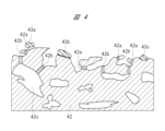
- the surface of the film 42 is in a state of having irregularities, pores, and surface-adhering foreign matter.
- the surface-adhering foreign matter includes a water-adsorbed substance 43 a that is adsorbed by water on the surface of the film 42 and between the film 42 and the film 42 .
- the surface-adhering foreign matter includes an electrostatically attracted matter 43b that is electrostatically attracted to the surface of the film 42.
- the surface-adhering foreign matter there is a stress-fixed substance 43c that is stress-fixed by the unevenness of the surface of the film 42.
- FIG. Many of these surface-adhering foreign substances are foreign substances separated from the film 42 in the polishing step of the first post-treatment or the like, and their materials are the same as the materials of the film 42 .
- the narrow portion 42a is a part of the film 42, but is a portion having a small thickness and thus weakly bonded to the surroundings. Surface contaminants are generated by breaking or dissolving the narrow portion 42a.
- the ultrasonic cleaning (step S10) in the dilute nitric acid of the present embodiment removes these surface-adhered foreign matter and the narrow portion 42a, resulting in the generation of foreign matter due to the surface state of the film after the post-treatment. to prevent
- Fig. 5 shows the dilute nitric acid ultrasonic cleaning time and yttrium elution rate.
- the elution rate referred to here is the elution amount (weight) of yttrium eluted per unit time from the measurement point (marker) before the relevant time to the relevant time.
- the example of the present embodiment is a graph consisting of plots of black squares, and the graph will be described here.
- Each graph shown in FIG. 5 is obtained by averaging a plurality of plots for each predetermined time.
- the elution rate of yttrium greatly decreases.
- the water adsorbate 43a and the electrostatically adsorbate 43b shown in FIG. 4 are eluted and separated from the surface of the film 42, and the removal of these substances greatly reduces the elution rate of yttrium. .
- the elution rate of yttrium which had decreased, once increased and then decreased.
- the remaining electrostatically attracted objects 43b and the stress-fixed objects 43c shown in FIG. 4 are eluted and separated.
- the pinched portion 42a is eluted, and along with this, the tip portion connected to the pinched portion 42a is separated from the film 42 and eluted. Therefore, in the second phase 1B, the elution rate of yttrium, which had decreased, increases once. After that, the elution rate decreases due to the decrease due to the elution of the foreign matter adhering to the surface and the elution of the pinched portion 42a.
- the elution rate of yttrium greatly increases from about 60 minutes after the start of dilute nitric acid ultrasonic cleaning, entering the third phase 1C.
- the elution rate of yttrium increases by 1.5 times or more compared to immediately before. This is because the thin portion 42b shown in FIG. 4 dissolves and the pores 42c are released, thereby increasing the surface area of the film 42.
- the pure water cleaning in step S11 is performed, and the ground electrode installed in the plasma processing apparatus is in a state where foreign matter is likely to be released from the film 42 .
- the dilute nitric acid ultrasonic cleaning should be stopped before the elution rate starts to increase in the third aspect 1C.
- the ground electrode to be cleaned is immersed in a diluted nitric acid solution, and ultrasonic irradiation is started to increase the elution rate of yttrium. Washing is stopped after the (elution amount) decreases (first phase 1A), increases again, decreases again (second phase 1B), and then increases again (third phase 1C).
- the cleaning step the elution rate of yttrium is detected during cleaning, and the elution rate of yttrium after the start of ultrasonic irradiation undergoes a first decrease, a first increase, and a second decrease in order. and stop washing before the second increase occurs.
- cleaning is stopped 10 minutes or 20 minutes after the start of ultrasonic irradiation and before 60 minutes have passed.
- the source of foreign matter on the surface of the inner wall material generated in the post-treatment after film formation can be removed, and the post-treatment can be completed in a state in which the exposure of the pores 42c is suppressed. That is, since the surface area of the film 42 can be prevented from increasing excessively, it is possible to suppress the generation of foreign substances due to the surface condition of the film 42 after the ground electrode is installed in the plasma processing apparatus. As a result, it is possible to improve the reliability of the method for cleaning the protective film for the plasma processing apparatus.
- elution rate elution amount
- these elution rates serve as criteria for determining whether or not cleaning is completed at the desired timing, or when it is time to terminate cleaning.
- the quality of the film 42 can be managed.
- the concentration of dilute nitric acid used in the dilute nitric acid ultrasonic cleaning described above will be explained.
- FIG. 5 an example of this embodiment is indicated by the black square plot.
- the concentration of dilute nitric acid is set to an intermediate level (0.001 mol/liter or more and 0.05 mol/liter or less).
- a graph composed of plotted black circles is a graph of a comparative example in which the concentration of dilute nitric acid was set higher than 0.05 mol/liter.
- a graph composed of black triangle plots is a graph of a comparative example in which the concentration of dilute nitric acid is set lower than 0.001 mol/liter.
- a graph of white circles is a graph of a comparative example in which an object is immersed in pure water instead of dilute nitric acid and subjected to ultrasonic cleaning.
- the dilute nitric acid ultrasonic cleaning of the present embodiment in which cleaning is stopped after the initial increase in the elution rate and before the elution rate increases again. Therefore, in order to separate the first phase 1A and the second phase 1B, the dilute nitric acid concentration must be 0.05 mol/liter or less.
- the increase in the third aspect 1C occurs before the increase in the dissolution rate confirmed in the second aspect 1B of the example of the present embodiment occurs. That is, the third phase 1C (irradiation upper limit) is reached only by physical destruction by ultrasonic waves. For this reason, it is difficult to perform the dilute nitric acid ultrasonic cleaning of the present embodiment in which the cleaning is stopped after the initial increase in the elution rate and before the elution rate increases again. Furthermore, since the narrow portion 42a and the stress fixing object 43c in the second phase 1B cannot be removed, sufficient cleaning cannot be performed. Therefore, the diluted nitric acid concentration should be 0.001 mol/liter or more.
- the table in FIG. 6 shows the results of the experiments conducted by the present inventors.
- the table of FIG. 6 shows the number of foreign substances falling on the wafer surface when plasma etching is performed using the plasma processing apparatus 100 shown in FIG.
- prior art 1 no post-treatment
- the foreign matter amount was 5.67.
- the present invention can be widely used in cleaning methods for protective films for plasma processing equipment.
Landscapes
- Engineering & Computer Science (AREA)
- Physics & Mathematics (AREA)
- Plasma & Fusion (AREA)
- Chemical & Material Sciences (AREA)
- Analytical Chemistry (AREA)
- Epidemiology (AREA)
- Health & Medical Sciences (AREA)
- Public Health (AREA)
- General Physics & Mathematics (AREA)
- Manufacturing & Machinery (AREA)
- Computer Hardware Design (AREA)
- Microelectronics & Electronic Packaging (AREA)
- Power Engineering (AREA)
- Condensed Matter Physics & Semiconductors (AREA)
- Drying Of Semiconductors (AREA)
- Chemical Vapour Deposition (AREA)
- Cleaning Or Drying Semiconductors (AREA)
Abstract
信頼性の高いプラズマ処理装置用保護皮膜の洗浄方法を提供する。その手段として、真空容器内部に配置された処理室内に載置された処理対象のウエハを当該処理室内に形成したプラズマを用いて処理するプラズマ処理装置の処理室内部に配置された基材の表面に形成され、プラズマに対する耐性を有する材料を含むプラズマ処理装置用保護皮膜の洗浄方法であって、(a)表面にイットリウムを含む皮膜を備えた基材を用意する工程、(b)基材を希硝酸液に浸漬し、皮膜に対し超音波照射を行うことで洗浄を行う工程、を有し、(b)工程では、洗浄中にイットリウムの溶出速度を検出し、超音波照射を開始してからのイットリウムの溶出速度が、順に第1減少、第1増加、第2減少を経た後であって、第2増加が起きる前に洗浄を停止する。
Description
本発明はプラズマ処理装置用保護皮膜の洗浄方法に関するものである。
電子デバイスや磁気メモリの製造において、微細加工には、プラズマエッチングが適用されている。プラズマエッチングを行うプラズマ処理装置の処理室内壁はエッチングプロセス時に高周波プラズマとエッチングガスに曝されるため、内壁表面は耐プラズマ性に優れた皮膜を形成し保護している。
特許文献1(特開2009-176787号公報)には、プラズマエッチング装置のアース部皮膜材料を、Al2O3、YAG、Y2O3、Gd2O3、Yb2O3またはYF3のいずれか一種類、もしくは2種類以上で構成することが記載されている。また、特許文献2(特開2017-31457号公報)には、表面に溶射皮膜が製膜された基材を有機酸に浸漬する洗浄方法が記載されている。
耐プラズマ性を有する上記皮膜は、表面粗さ(Ra)および気孔率を低く抑えることが求められているため、皮膜形成後にその表面を研磨するなどの後処理が行われる。しかし、後処理により、肉厚の薄い領域または静電気吸着した内壁材などを原因とする表面付着異物の放出により、エッチング対象に異物が付着し易くなる。そのため、後処理後の異物発生を低くする洗浄方法が必要となっている。
本発明の目的は、信頼性の高いプラズマ処理装置用保護皮膜の洗浄方法を提供することにある。
その他の目的と新規な特徴は、本明細書の記述および添付図面から明らかになるであろう。
本願において開示される実施の形態のうち、代表的なものの概要を簡単に説明すれば、次のとおりである。
代表的な実施の形態によるプラズマ処理装置用保護皮膜の洗浄方法は、真空容器内部に配置された処理室内に載置された処理対象のウエハを当該処理室内に形成したプラズマを用いて処理するプラズマ処理装置の処理室内部に配置された基材の表面に形成され、プラズマに対する耐性を有する材料を含むプラズマ処理装置用保護皮膜の洗浄方法であって、(a)表面にイットリウムを含む皮膜を備えた基材を用意する工程、(b)基材を希硝酸液に浸漬し、皮膜に対し超音波照射を行うことで洗浄を行う工程、を有し、(b)工程では、洗浄中にイットリウムの溶出速度を検出し、超音波照射を開始してからのイットリウムの溶出速度が、順に第1減少、第1増加、第2減少を経た後であって、第2増加が起きる前に洗浄を停止するものである。
代表的な実施の形態によれば、信頼性の高いプラズマ処理装置用保護皮膜の洗浄方法を提供することが可能となる。
以下、本発明の実施の形態を図面に基づいて詳細に説明する。なお、実施の形態を説明するための全図において、同一の機能を有する部材には同一の符号を付し、その繰り返しの説明は省略する。また、実施の形態では、特に必要なときを除き、同一または同様な部分の説明を原則として繰り返さない。
<改善の余地の詳細>
電子デバイスなどの製造工程では、プラズマエッチングが適用される場合がある。プラズマエッチングに用いられるプラズマ処理装置の処理室は、真空容器内部に配置されるため、アルミニウム、ステンレス等の金属から構成されている。プラズマ処理装置の処理室内壁はエッチングプロセス時に高周波プラズマとエッチングガスに曝されるため、内壁表面には耐プラズマ性に優れた皮膜を形成し保護する。このような保護皮膜としては、酸化イットリウム製の皮膜が用いられることが考えられる。
電子デバイスなどの製造工程では、プラズマエッチングが適用される場合がある。プラズマエッチングに用いられるプラズマ処理装置の処理室は、真空容器内部に配置されるため、アルミニウム、ステンレス等の金属から構成されている。プラズマ処理装置の処理室内壁はエッチングプロセス時に高周波プラズマとエッチングガスに曝されるため、内壁表面には耐プラズマ性に優れた皮膜を形成し保護する。このような保護皮膜としては、酸化イットリウム製の皮膜が用いられることが考えられる。
処理室での異物発生は、エッチング対象への異物付着に起因した製造不良を引き起こし、歩留まりの低下の原因となる。このため、処理室での異物発生を抑制することが重要である。処理室内における異物発生は、内壁材の結晶サイズや相比率と相関がある。
酸化イットリウムを材料として含む上記皮膜は、例えば大気プラズマ溶射法などを用いて製膜される。大気プラズマ溶射法では、10~60μmサイズの原料粉を輸送ガスと伴にプラズマ炎に導入し、溶融、半溶融状態になった原料粒子を基材表面に噴射して付着させて膜を形成する。一方で、このプラズマ溶射法は、表面凹凸が大きいこと、または膜の内部に多数の気孔が形成され、これらの気孔内部に進入した粒子が膜自体または他の部材と反応を生起して、膜を消耗または腐食を生起させる原因となるなどの課題がある。
このため、上記皮膜については、表面粗さ(Ra)および気孔率を低く抑えることが求められている。そこで、皮膜形成後には、研磨などによる後処理が行われる。しかし、この後処理により、皮膜の肉厚の薄い領域または皮膜に静電気吸着した内壁材などを原因とする表面付着異物がプラズマエッチング装置の稼働初期に放出される場合がある。そのため、後処理後の異物発生を低くする洗浄方法と、後処理の良否の検査方法が必要となっている。
大気プラズマ溶射法は、製膜時に空気を巻き込んだり、急冷による割れが発生する製膜方法である。このため、皮膜の表面は、これら原因とする表面凹凸および埋もれた気孔(空隙)を含んでいる。すなわち、皮膜の表面には周囲より密着性の弱い部分が生じる。また、凹凸低減を目的として上記研磨処理を行うと、埋もれた気孔が開口して肉厚が薄い部分が生じる場合、または、研磨で除去された皮膜材が静電気で表面に再付着する場合がある。そのため皮膜は、これらを原因とする初期異物が発生し易い表面状態になっている。
また、後処理の良否の検査方法の1つとしては、処理室の内壁を構成する部材の表面の皮膜に対しては、その膜の形成後あるいは後処理後の当該皮膜の気孔率、表面粗さ(Ra)、結晶子のサイズ、相比率等の値を検出し、これらを予め定められた仕様の許容範囲と比較して評価する方法がある。
しかし、上記検査方法は、皮膜を形成後にその気孔率、表面粗さ(Ra~算術平均粗さ)、結晶子サイズ、相比率等の膜の特性について所定の許容範囲と比較し評価することは行われず、例えば、当該部材の検査は外観の検査のみに留まる。また、内壁を構成する部材の表面に形成された皮膜が部材個々の配置された箇所において、所期の特性および性能(気孔率、表面粗さ、残留応力、結晶子サイズ、相比率など)を有しているか否かは判明しない。そのため、上記検査を行うのみでは、洗浄工程の信頼性を高めることは困難である。
また、後処理の良否を調べる他の検査方法としては、処理室の内部の部材からその一部を切り出して検査を行う方法がある。しかし、この検査方法では、検査を行う対象の部材の一部分を部材から切断した後に当該部分を洗浄するなどの作業が必要となる。このため、検査の対象となる部分の皮膜は、同じ種類の他の部材のものとは同じ過程で形成されたものではなくなる。さらに、切断する工程において検査の対象となる皮膜の表面に異物が発生し、検査の精度が損なわれる虞がある。
また、後処理の良否を調べる他の検査方法としては、ある種類の部材複数の表面に溶射により皮膜が形成される場合に、任意の1個の部材と他の部材とでできるだけ同じ性能または形状等特性を有した皮膜が形成されるされるように、部材の一部を切り出して検査に用いたり、複数個製作する製品の1個を検査に用いる方法がある。しかし、この検査方法では、部材の寸法が大きいと、部材の単価が大きくなり、検査の実施のためにプラズマ処理装置の製造コストが増大する。
以上のように、上記技術では、プラズマ処理装置の信頼性や処理の歩留まりが損なわれており、また、製造のコストの増大の原因となっていた。
このため、プラズマ処理装置用保護皮膜の洗浄工程については、当該洗浄工程を含む後処理後の異物発生を抑制することよる洗浄方法の信頼性の向上という改善の余地がある。
(実施の形態)
本発明の実施の形態に係るプラズマ処理装置の構成を、図1および図2を用いて説明する。図1は、本発明の実施の形態に係るプラズマ処理装置の構成の概略を模式的に示す縦断面図である。本図に示すプラズマ処理装置は、真空容器内部の処理室内にプラズマを形成して当該処理室内に配置された半導体ウエハなどの試料の表面に予め形成されたマスク層およびその下方の処理対象の膜層とを有する膜構造をプラズマを用いてエッチング処理するプラズマエッチング装置である。
本発明の実施の形態に係るプラズマ処理装置の構成を、図1および図2を用いて説明する。図1は、本発明の実施の形態に係るプラズマ処理装置の構成の概略を模式的に示す縦断面図である。本図に示すプラズマ処理装置は、真空容器内部の処理室内にプラズマを形成して当該処理室内に配置された半導体ウエハなどの試料の表面に予め形成されたマスク層およびその下方の処理対象の膜層とを有する膜構造をプラズマを用いてエッチング処理するプラズマエッチング装置である。
図1に示す実施の形態のプラズマ処理装置100は、一部が円筒形を有する金属製の真空容器1を有している。また、プラズマ処理装置100は、真空容器1の上部に配置され真空容器1内部の減圧された空間にプラズマを形成するための電界または磁界を生起する生成器を有し生起された電界または磁界を内部空間に供給するプラズマ形成部を有している。また、プラズマ処理装置100は、真空容器1下部に配置されて真空容器1と接続され真空容器1内部の空間を排気して減圧する真空ポンプを有する排気部を有している。真空容器1は、その外側の側壁が別の真空容器1であって処理対象の試料であるウエハが減圧された内部の搬送用の空間で搬送される搬送容器と連結される。真空容器1の側壁には当該側壁を水平方向に貫通して真空容器1内部と外部とを連通する通路であってウエハが内側を通り搬送されるゲートが備えられている。当該ゲートの外側の開口部の外周を囲む真空容器1の側壁の箇所において、搬送容器が連結されて真空容器1の内部の空間と搬送容器内部の空間とが連通可能に構成される。
真空容器1は内部に処理対象の試料が配置されプラズマが形成される空間である処理室7を有している。処理室7は上部に配置され円筒形を有してプラズマ15が形成される放電部を有し、放電部と連通された下部の空間内には円筒形を有した試料台であるステージ6が配置されている。ステージ6には、被処理基板となるウエハ4が載置される面である円形の上面を有している。また、ステージ6は、その内部にウエハ4を加熱するヒータと冷却する冷媒が内部を通流する冷媒流路が配置されると共に、ステージ6の円形の上面と当該上面に載せられたウエハ4の裏面との間に伝熱ガスであるヘリウム(He)ガスを供給するための管路を備えている。
さらに、ステージ6の内部には金属製の電極が配置されて、プラズマ15を用いたウエハ4の処理中にウエハ4上に電位を形成するための高周波電力を当該電極に供給する高周波電源14がインピーダンス整合器13を介して電気的に接続されている。プラズマ15の形成中に高周波電力によりウエハ4上に形成されるバイアス電位とプラズマとの電位差によりウエハ4の表面にウエハ4内部のイオン等荷電粒子が誘引されエッチング処理が促進される。
ウエハ4は搬送容器内部の搬送用の空間内に配置されたロボットアーム等の搬送装置(図示しない)のアームの先端部に載せられて処理室7に搬送された後、ステージ6上に載置される。ステージ6に載置されたウエハ4は、静電吸着用の電極に直流電圧が印加されることによって生起された静電気力により誘電体製の皮膜上面に吸着されて保持される。
真空容器1の放電部を囲む円筒形の側壁部材の上端部の上方には、円板形状を有したシャワープレート2および窓部材3がリング状の部材を挟んで載せられている。窓部材3は放電部外周の側壁部材41と共に真空容器1を構成する。窓部材3の外周縁部の下面と側壁部材の上端部上面とこれらの間に配置されたリング状部材同士の間には、Oリング等のシール部材が挟まれてこれらの部材が接続されて、真空容器1内部の処理室7と外部の大気圧の雰囲気との間が気密に区画される。
窓部材3は、後述のように、プラズマ15を形成するためのマイクロ波の電界が透過するセラミクス(本実施の形態では石英)から構成された円板状の部材で、その下方には所定の大きさの間隙8をあけて、複数の貫通穴9が中央部に備えられたシャワープレート2が配置されている。シャワープレート2は処理室7の内部に面してその天井面を構成し、ガス流量制御手段(図示しない)で流量が所定の値に調節された処理ガスが間隙8内部に導入され、間隙8内で拡散した後貫通孔を通して処理室7内部に上方から導入される。なお、処理ガスは、リング状部材に接続された処理ガス供給配管50上に配置されたバルブ51が開いて間隙8に導入される。
また、真空容器1の底部には処理室7内部と外部とを連通して、処理室7内部のプラズマ15やウエハ4の処理中に生成された生成物、処理ガスの粒子が排出される通路が備えられている。当該通路の処理室7内側の円形の開口は排気口として上方に配置されたステージ6の直下方で中心軸同士が上方から見て同じと見なせる位置に配置されている。真空容器1の底面には、排気部の真空ポンプを構成するターボ分子ポンプ12およびターボ分子ポンプ12の下流側に配置されたドライポンプ11が連結されている。さらに、ターボ分子ポンプ12の入り口は排気口と排気配管で接続されている。
ターボ分子ポンプ12とドライポンプ11との間を連結する排気配管上にはバルブ18が配置され、バルブ18とドライポンプ11との間の排気配管の箇所には、真空容器1の底面に接続されて処理室7の底部と連通された別の排気配管10が接続されている。この別の排気配管10はその途中に2つの管路に分岐した後再度1つに合流するように接続され、分岐部の各々上にはバルブ17、19が配置されている。バルブ17とバルブ19のうち、バルブ17は、処理室7を大気圧から真空にドライポンプ11でゆっくり排気するためのスロー排気用のバルブであり、バルブ19は、ドライポンプ11で高速に排気するためのメイン排気用のバルブである。
処理室7には、その内部の圧力を検出するための圧力センサ75が備えられている。本実施の形態の排気口の上方であってステージ6の底面との間の処理室7の下部の空間には、この空間内で上下方向に移動して排気口を開閉すると共に排気口の開口面積を増減させ排気の流量またはその速度を調節する円板形状を有した圧力調整板16が配置されている。処理室7内の圧力は、シャワープレート2の貫通孔であるガス導入口を通して処理室7内に導入される処理ガスあるいは他のガスと排気口からの排気との流量または速度のバランスにより増減される。例えば、処理室7内にシャワープレート2からガスが流量または速度をウエハ4の処理の条件に応じた所定の値にされて導入されつつ、圧力調整板16が上下方向の位置を調整されることで当該処理の条件に応じた処理室7の圧力が実現されるように排気の流量または速度が調節される。
真空容器1上部の処理室7の放電部外周を囲む金属製の側壁および窓部材3の上方と外周側の箇所にはプラズマ形成部が配置されている。プラズマ形成部は、プラズマ15を形成するためのマイクロ波の電界を出力するマグネトロン発振器20と、マイクロ波を処理室7まで伝搬させるための導波管21とを有している。導波管21は、水平方向(図上左右方向)に延在して断面が矩形または方形を有した方形部と、方形部の一端部に接続され上下方向に延在する円筒形状を有した円形部とを有し、方形部の他端部にはマグネトロン発振器20が配置されている。
円形部の下端は、窓部材3の上方に配置され円形部の直径より大きい窓部材3と同じと見做せる程度の近似した大きさの直径を有した円筒形の空洞部の上端と接続されている。さらに、空洞部の上方とその外周側および放電部を囲む真空容器1の側壁の外周側で処理室7の放電部を囲む箇所には、直流電力が供給され磁界を発生する手段であるリング状のソレノイドコイル22、23が備えられている。
処理室7の側壁部材41の内側の壁面は放電部内に形成されるプラズマ15に曝される面であるが、プラズマ15の電位を安定させるために処理室7内にアースとして機能する部品を有する必要がある。本実施の形態では、放電部内にアースとして機能するリング状のアース電極40がステージ6の上方でステージ6上面を囲んで配置されている。アース電極40は、ステンレス合金またはアルミニウム合金などの金属製の部材を母材として構成されている。アース電極40は、プラズマ15に曝されるため、プラズマ15内の反応性または腐食性の高い粒子との相互作用を受けて、生成した生成物による腐食、金属汚染または異物の発生源となる虞が高い。
そのため、このような問題を抑制するため、図1の左下部分に拡大して示される断面図に模式的に示されるように、本実施の形態のアース電極40の表面には耐プラズマ性の高い材料から成る皮膜42が、アース電極40の表面を覆って配置されている。皮膜42が当該表面を覆うことによって、アース電極40は、アースとして機能を維持しつつプラズマによるアース電極40への腐食等のダメージを抑制することができる。なお、皮膜42は積層膜でもよい。
一方、本実施の形態の真空容器1の放電部を囲む側壁部材41は、ステンレス合金またはアルミニウム合金等の金属製の基材から構成されているものの、アースとしての機能を有さない。側壁部材41がプラズマ15に曝されることにより腐食や金属汚染、異物が発生することを抑制するため、側壁部材41の内側表面には不動態化処理、溶射、PVDまたはCVDなどの表面処理が施されている。また、側壁部材41の基材が直接にプラズマ15に曝されることを防止するため、以下のようなセラミクス製の部品が形成されていてもよい。すなわち、円筒形状を有した側壁部材41の内側側壁面と処理室7の放電部との間に、リング状または円筒形状を有した例えば酸化イットリウムや石英等のセラミクス製の部品が、内側側壁面に沿って当該内側壁面をプラズマ15に対して覆うように配置されていてもよい。側壁部材41とプラズマ15との間の当該部品によって、側壁部材41とプラズマ15との接触が阻害され、プラズマ15による表面処理された側壁部材41の消耗が抑制される。
図2は、図1に示すアース電極を構成する部品の構成の概略を模式的に示す斜視図である。図2では、図1に示すリング状あるいは円筒形状を有するアース電極40を斜め下側の箇所から上側に向けて見た場合の図を示している。
本図に示すように、アース電極40は全体が所定の厚さを有した円筒形を備え、上下方向の中心軸周りに各々同じ値の内径を有する内側側壁と外側側壁とを有している。さらに、アース電極40は円筒形の主側壁部分と主側壁部分の上端からさらに上方に配置されたリング形状の電極部とを備えており、電極部の外周壁面は上下方向の中心軸からの半径位置が下方の主側壁部分より小さくされている。円筒形の主側壁部分の上下方向の中段部分には、ゲート49を構成する貫通孔の矩形状の開口部43が配置されている。
アース電極40が処理室7内部に取り付けられた状態で、アース電極40は、内側側壁と処理室7との間に配置される。アース電極40は、下部がステージ6の外周側でこれを囲む真空容器1の側壁部材41の内側壁面をプラズマ15に対して覆い、上部が放電部を囲む側壁部材41の内側に配置されて当該側壁部材41の内側壁面をプラズマ15に対して覆うだけの上下方向の長さを有している。この形状により、側壁部材41をプラズマ15の相互作用から保護する。
<プラズマ処理装置用保護皮膜の形成方法および洗浄方法>
次に、本実施の形態に関し、皮膜(溶射皮膜)の形成から、皮膜形成後の後処理を行う工程について、図3~図5を用いて説明する。
次に、本実施の形態に関し、皮膜(溶射皮膜)の形成から、皮膜形成後の後処理を行う工程について、図3~図5を用いて説明する。
図3のフローでは、プラズマ処理装置用のアース電極を保護する耐プラズマ性の皮膜の形成工程(従来技術1)と、当該皮膜の形成後に行う第1後処理(従来技術2)と、第2後処理(本実施の形態の実施例)とを行う手順を示すものである。
ここでは、まず、アース電極を用意し、アース電極の表面の脱脂処理を行う(ステップS1)。ここで用意し、脱脂処理するアース電極は、図1のプラズマ処理装置100に組み込まれる前の単体の電極である。
次に、アース電極の表面に対し、皮膜形成の前処理としてサンドブラスト処理を行う(ステップS2)。ここでは、アース電極に対して研磨材(粒子)の吹き付けを行う。これにより、アース電極の表面の清浄化および粗面化を行うことで、後に形成する皮膜の密着性を向上させる。次に、アース電極の表面の脱脂処理を行う(ステップS3)。
次に、アース電極の表面に、大気プラズマ溶射(APS:Atmospheric Plasma Spraying)法により皮膜を形成する(ステップS4)。ここでは、YF3(フッ化イットリウム)から成る皮膜を形成する。皮膜の材料は、その他に、YOF(オキソフッ化イットリウム)、Y2O3(オキソイットリウム)またはYAG(Yttrium Aluminum Garnet)を用いてもよい。大気プラズマ溶射法は大気圧にされた雰囲気中において皮膜を対象物の表面に溶射により形成する方法であり、大気中に形成したプラズマで原料粉を溶融させて溶融または半溶融状態の原料を対象物表面に吹き付けて積層させ皮膜を形成する。ここまでのステップS1~S4の工程を、従来技術1とする。
次に、皮膜が形成されたアース電極を純水中に浸漬し、超音波洗浄を行う(ステップS5)。次に、アース電極に対し薬液処理を行い(ステップS6)、その後、再度アース電極を純水中に浸漬して超音波洗浄を行う(ステップS7)。次に、アース電極に対し研磨処理を行い(ステップS8)、その後、再度アース電極を純水中に浸漬して超音波洗浄を行う(ステップS9)。ここまでのステップS5~S9の工程(第1後処理)を、従来技術2とする。
次に、皮膜を備えたアース電極を希硝酸中に浸漬し、これに対し超音波照射を行う(ステップS10)。次に、アース電極に対し純水洗浄を行う(ステップS11)。ここまでのステップS10、S11の工程(第2後処理)を、本実施の形態の実施例とする。以上により、皮膜の形成と後処理(第1後処理および第2後処理)とを終了する。この後、アース電極40は、図1に示すプラズマ処理装置100に組み込まれる。
本実施の形態では、従来行っていた皮膜形成工程(ステップS1~S4)および第1後処理(ステップS5~S9)に加えて、希硝酸中における超音波洗浄(ステップS10)を、以下に説明する条件で行うことを主な特徴とするものである。すなわち、本実施の形態は、希硝酸中で超音波照射を行う洗浄により、周囲との結合が弱い部分を酸溶解と超音波振動により除去することに主な特徴がある。
図4に示すように、第1後処理を終えた後(ステップS9の直後)において、皮膜42の表面は、凹凸、気孔および表面付着異物を有する状態となっている。表面付着異物としては、具体的には、皮膜42の表面において、皮膜42との間に水により吸着している水吸着物43aがある。また、表面付着異物としては、皮膜42の表面に対し静電吸着している静電吸着物43bがある。また、表面付着異物としては、皮膜42の表面の凹凸により応力固定された応力固定物43cがある。これらの表面付着異物の多くは、第1後処理の研磨工程などで皮膜42から分離した異物であり、それらの材料は皮膜42の材料と同じである。
また、狭弱部42aは、皮膜42の一部であるが、厚さが小さい部分であるために周囲との結合が弱い部分である。狭弱部42aが折れたり溶解することで、表面異物が発生する。本実施の形態の希硝酸中での超音波洗浄(ステップS10)は、これらの表面付着異物と狭弱部42aを除去することで、後処理の後に皮膜の表面状態に起因して異物が発生することを防ぐものである。
しかし、希硝酸中での超音波洗浄を長時間行うと、洗浄開始時には表面に露出してない内部の気孔42cが、当該洗浄により開口され、表面積が増加する。すなわち、皮膜42の表面近傍の皮膜42内には、気孔42cが多数形成されている。皮膜42の表面に特に近い気孔42cと当該表面との間には、皮膜42の一部であって厚さの小さい薄部42bが存在する。このような薄部42bが長時間の希硝酸超音波洗浄により溶解すると、薄部42bが形成されていた箇所が開口部となり、気孔42cが解放される。その結果、皮膜42の表面積が増加する。
希硝酸超音波洗浄の時間とイットリウムの溶出速度について、図5に示す。ここでいう溶出速度は、該当時間の前の測定点(マーカ)から該当時間までに溶出したイットリウムの単位時間当たりの溶出量(重さ)である。図5に示すグラフのうち、本実施の形態の実施例は、黒い四角のプロットから成るグラフであり、ここでは当該グラフに関し説明する。なお、図5に示す各グラフは、複数のプロットを所定の時間毎に平均化したものである。
図5に示すように、希硝酸超音波洗浄を開始すると、まず、第1局面1Aとして、イットリウムの溶出速度が大きく減少する。この第1局面1Aでは、図4に示す水吸着物43aと静電吸着物43bとが皮膜42の表面から溶出、分離されるのであり、それらの除去によりイットリウムの溶出速度が大きく減少している。
希硝酸超音波洗浄の開始から10分前後の第2局面1Bでは、減少していたイットリウムの溶出速度が一旦増加し、その後減少する。第2局面1Bでは、図4に示す残りの静電吸着物43bと、応力固定物43cが溶出、分離される。さらに、第2局面1Bでは、挟弱部42aが溶出し、これに伴い挟弱部42aに接続されていた先端部が皮膜42から分離して溶出する。このため、第2局面1Bでは、減少していたイットリウムの溶出速度が一旦増加する。その後は、表面付着異物および挟弱部42aの溶出などによる減少により、溶出速度は減少する。
ここで、さらに希硝酸超音波洗浄を続けると、希硝酸超音波洗浄の開始から60分を経過した頃から、イットリウムの溶出速度が大きく増加する第3局面1Cに入る。第3局面1Cでは、その直前に比べて、イットリウムの溶出速度が1.5倍以上に増加する。これは、図4に示す薄部42bが溶出して気孔42cが解放されることで皮膜42の表面積が増加することに起因している。このように皮膜42の表面積が増加した状態でステップS11の純水洗浄を行い、プラズマ処理装置に組み込んだアース電極は、皮膜42から異物が放出され易い状態にある。すなわち、希硝酸超音波洗浄を行う時間を規定せずに長時間希硝酸超音波洗浄を行うと、後処理を行ったにも関わらず、異物の発生を効果的に抑制できないことが考えられる。したがって、希硝酸超音波洗浄は、第3局面1Cにおける溶出速度の増加が始まる前に停止する必要がある。
そこで、本実施の形態の形態の主な特徴として、ステップS10における希硝酸超音波洗浄工程では、洗浄対象であるアース電極を希硝酸液に浸漬し、超音波照射を開始してイットリウムの溶出速度(溶出量)が、減少(第1局面1A)した後、再度増加して再度減少(第2局面1B)した後、再度増加(第3局面1C)が起きる前に、洗浄を停止する。言い換えれば、当該洗浄工程では、洗浄中にイットリウムの溶出速度を検出し、超音波照射を開始してからのイットリウムの溶出速度が、順に第1減少、第1増加、第2減少を経た後であって、第2増加が起きる前に洗浄を停止する。例えば、本実施の形態では、超音波照射を開始してから10分または20分経過後であって、60分が経過するまでに洗浄を停止する。
これにより、皮膜製膜後の後処理で発生した内壁材表面の異物源を除去し、かつ、気孔42cの露出を抑制した状態で後処理を終了することができる。すなわち、皮膜42の表面積が過剰に増加することを防げるため、アース電極をプラズマ処理装置に組み込んだ後に皮膜42の表面状態に起因する異物発生を抑制できる。この結果、プラズマ処理装置用保護皮膜の洗浄方法の信頼性を高めることができる。
また、第1局面1Aと第2局面1Bのそれぞれのイットリウムの溶出速度(溶出量)を求め、付着異物指標とすることで、洗浄の検査指標として利用できる。つまり、それらの溶出速度は、洗浄が所望のタイミングで終了しているかどうか、または、洗浄を終了すべきタイミングがいつであるかの判定基準となる。これにより、皮膜42の品質を管理することができる。このような洗浄を行ったアース電極を用いることで、プラズマ処理装置の処理室内の異物の発生を抑制し、ウエハの処理の歩留まりを向上することができる。以上より、上記した改善の余地を解消できる。
ここで、上述した希硝酸超音波洗浄で用いる希硝酸の濃度について説明する。図5において、本実施の形態の実施例は、黒い四角のプロットにより示されている。ここでは、希硝酸の濃度は中程度(0.001mol/リットル以上、0.05mol/リットル以下)に設定されている。また、黒い丸のプロットから成るグラフは、希硝酸の濃度が0.05mol/リットルより高く設定された比較例のグラフである。また、黒い三角のプロットから成るグラフは、希硝酸の濃度が0.001mol/リットルより低く設定された比較例のグラフである。また、白い丸のプロットから成るグラフは、希硝酸ではなく純水に対象物を浸漬して超音波洗浄した場合の比較例のグラフである。
純水での超音波洗浄(白い丸のグラフ)で示すように、希硝酸を用いずとも、第1局面1Aでは溶出速度が大きく低下し、第3局面1Cでは物理破壊により気孔42cは露出するため、イットリウムの溶出速度は増加する。また、希硝酸濃度が高い場合(黒い丸のグラフ)、本実施の形態の実施例の第2局面1Bで確認できた溶出速度の増加が、第1局面1A側に近いタイミングで発生するため、最初の溶出速度の増加を確認することが困難となる。その場合、最初の溶出速度の増加の後、再増加の前に洗浄を停止するという本実施の形態の希硝酸超音波洗浄を行うことが困難となる。したがって、第1局面1Aと第2局面1Bとを分離するために、希硝酸濃度は0.05mol/リットル以下である必要がある。
また希硝酸濃度が低い場合(黒い三角のグラフ)、本実施の形態の実施例の第2局面1Bで確認できた溶出速度の増加が生じる前に、第3局面1Cでの増加を起きる。つまり、超音波による物理破壊だけで第3局面1C(照射上限)に達しする。このため、最初の溶出速度の増加の後、再増加の前に洗浄を停止するという本実施の形態の希硝酸超音波洗浄を行うことが困難となる。さらに、第2局面1Bにおける狭弱部42aおよび応力固定物43cの除去ができないため、十分な洗浄を行えない。したがって、希硝酸濃度は、0.001mol/リットル以上とする必要がある。
図6の表に、本発明者らが行った実験の結果を示す。図6の表には、図1に示すプラズマ処理装置100を用いてプラズマエッチングを行った場合に、ウエハの表面に落ちる異物物の個数を示している。従来技術1(後処理なし)の場合、つまり、図3のステップS4でアース電極および皮膜の準備工程を終了し、第1後処理および第2後処理を行わない場合には、異物量は100を超える。また、第1後処理を行う従来技術2の場合、つまり、図3のステップS9で後処理を終了する場合には、異物量は5.67であった。
これに対し、第1後処理に続いて第2後処理を行った本実施の形態の実施例の場合、つまり、図3のステップS11で後処理を終了した場合には、異物量は3.76であった。このように、希硝酸超中で超音波照射を開始し、イットリウムの溶出速度が、減少した後、再度増加してから再度減少した後、再度増加が起きる前に洗浄を停止する後処理を行う本実施の形態では、異物源を効果的に除去できる。
以上、本発明者らによってなされた発明をその実施の形態に基づき具体的に説明したが、本発明は前記実施の形態に限定されるものではなく、その要旨を逸脱しない範囲で種々変更可能である。
本発明は、プラズマ処理装置用保護皮膜の洗浄方法に幅広く利用することができる。
1 真空容器
4 ウエハ
15 プラズマ
40 アース電極
41 側壁部材
42 皮膜
42a 狭弱部
42b 薄部
42c 気孔
43a 水吸着物
43b 静電吸着物
43c 応力固定物
100 プラズマ処理装置
4 ウエハ
15 プラズマ
40 アース電極
41 側壁部材
42 皮膜
42a 狭弱部
42b 薄部
42c 気孔
43a 水吸着物
43b 静電吸着物
43c 応力固定物
100 プラズマ処理装置
Claims (6)
- 真空容器内部に配置された処理室内に載置された処理対象のウエハを当該処理室内に形成したプラズマを用いて処理するプラズマ処理装置の処理室内部に配置された基材の表面に形成され、前記プラズマに対する耐性を有する材料を含むプラズマ処理装置用保護皮膜の洗浄方法であって、
(a)表面にイットリウムを含むプラズマ処理装置用保護皮膜を備えた前記基材を用意する工程、
(b)前記基材を希硝酸液に浸漬し、前記プラズマ処理装置用保護皮膜に対し超音波照射を行うことで洗浄を行う工程、
を有し、
前記(b)工程では、前記洗浄中にイットリウムの溶出速度を検出し、前記超音波照射を開始してからのイットリウムの溶出速度が、順に第1減少、第1増加、第2減少を経た後であって、第2増加が起きる前に洗浄を停止する、プラズマ処理装置用保護皮膜の洗浄方法。 - 請求項1記載のプラズマ処理装置用保護皮膜の洗浄方法において、
前記希硝酸液の希硝酸濃度は、0.05mol/リットル以下である、プラズマ処理装置用保護皮膜の洗浄方法。 - 請求項1記載のプラズマ処理装置用保護皮膜の洗浄方法において、
前記希硝酸液の希硝酸濃度は、0.001mol/リットル以上である、プラズマ処理装置用保護皮膜の洗浄方法。 - 請求項1記載のプラズマ処理装置用保護皮膜の洗浄方法において、
前記希硝酸液の希硝酸濃度は、0.001mol/リットル以上、0.05mol/リットル以下である、プラズマ処理装置用保護皮膜の洗浄方法。 - 請求項1記載のプラズマ処理装置用保護皮膜の洗浄方法において、
前記(b)工程では、前記超音波照射を開始してから60分経過前に洗浄を停止する、プラズマ処理装置用保護皮膜の洗浄方法。 - 請求項5記載のプラズマ処理装置用保護皮膜の洗浄方法において、
前記(b)工程では、前記超音波照射を開始してから30分経過後に洗浄を停止する、プラズマ処理装置用保護皮膜の洗浄方法。
Priority Applications (5)
| Application Number | Priority Date | Filing Date | Title |
|---|---|---|---|
| KR1020227029775A KR20230031187A (ko) | 2021-08-23 | 2021-08-23 | 플라스마 처리 장치용 보호 피막의 세정 방법 |
| CN202180017270.1A CN116018669A (zh) | 2021-08-23 | 2021-08-23 | 等离子处理装置用保护皮膜的清洗方法 |
| JP2022551293A JP7358655B2 (ja) | 2021-08-23 | 2021-08-23 | プラズマ処理装置用保護皮膜の洗浄方法 |
| PCT/JP2021/030850 WO2023026331A1 (ja) | 2021-08-23 | 2021-08-23 | プラズマ処理装置用保護皮膜の洗浄方法 |
| TW111129529A TW202309976A (zh) | 2021-08-23 | 2022-08-05 | 電漿處理裝置用保護皮膜之洗淨方法 |
Applications Claiming Priority (1)
| Application Number | Priority Date | Filing Date | Title |
|---|---|---|---|
| PCT/JP2021/030850 WO2023026331A1 (ja) | 2021-08-23 | 2021-08-23 | プラズマ処理装置用保護皮膜の洗浄方法 |
Publications (1)
| Publication Number | Publication Date |
|---|---|
| WO2023026331A1 true WO2023026331A1 (ja) | 2023-03-02 |
Family
ID=85321630
Family Applications (1)
| Application Number | Title | Priority Date | Filing Date |
|---|---|---|---|
| PCT/JP2021/030850 WO2023026331A1 (ja) | 2021-08-23 | 2021-08-23 | プラズマ処理装置用保護皮膜の洗浄方法 |
Country Status (5)
| Country | Link |
|---|---|
| JP (1) | JP7358655B2 (ja) |
| KR (1) | KR20230031187A (ja) |
| CN (1) | CN116018669A (ja) |
| TW (1) | TW202309976A (ja) |
| WO (1) | WO2023026331A1 (ja) |
Citations (4)
| Publication number | Priority date | Publication date | Assignee | Title |
|---|---|---|---|---|
| WO2007007782A1 (ja) * | 2005-07-14 | 2007-01-18 | Tohoku University | 多層構造体及びその洗浄方法 |
| JP2009174000A (ja) * | 2008-01-24 | 2009-08-06 | Shin Etsu Chem Co Ltd | セラミックス溶射部材及びその製造方法ならびにセラミックス溶射部材用研磨メディア |
| JP2017031457A (ja) * | 2015-07-31 | 2017-02-09 | 信越化学工業株式会社 | イットリウム系溶射皮膜、及びその製造方法 |
| JP2019519091A (ja) * | 2016-04-01 | 2019-07-04 | アプライド マテリアルズ インコーポレイテッドApplied Materials,Incorporated | オキシフッ化物を沈殿させるクリーニングプロセス |
Family Cites Families (1)
| Publication number | Priority date | Publication date | Assignee | Title |
|---|---|---|---|---|
| JP2009176787A (ja) | 2008-01-22 | 2009-08-06 | Hitachi High-Technologies Corp | エッチング処理装置及びエッチング処理室用部材 |
-
2021
- 2021-08-23 CN CN202180017270.1A patent/CN116018669A/zh active Pending
- 2021-08-23 WO PCT/JP2021/030850 patent/WO2023026331A1/ja active Application Filing
- 2021-08-23 JP JP2022551293A patent/JP7358655B2/ja active Active
- 2021-08-23 KR KR1020227029775A patent/KR20230031187A/ko unknown
-
2022
- 2022-08-05 TW TW111129529A patent/TW202309976A/zh unknown
Patent Citations (4)
| Publication number | Priority date | Publication date | Assignee | Title |
|---|---|---|---|---|
| WO2007007782A1 (ja) * | 2005-07-14 | 2007-01-18 | Tohoku University | 多層構造体及びその洗浄方法 |
| JP2009174000A (ja) * | 2008-01-24 | 2009-08-06 | Shin Etsu Chem Co Ltd | セラミックス溶射部材及びその製造方法ならびにセラミックス溶射部材用研磨メディア |
| JP2017031457A (ja) * | 2015-07-31 | 2017-02-09 | 信越化学工業株式会社 | イットリウム系溶射皮膜、及びその製造方法 |
| JP2019519091A (ja) * | 2016-04-01 | 2019-07-04 | アプライド マテリアルズ インコーポレイテッドApplied Materials,Incorporated | オキシフッ化物を沈殿させるクリーニングプロセス |
Also Published As
| Publication number | Publication date |
|---|---|
| JPWO2023026331A1 (ja) | 2023-03-02 |
| JP7358655B2 (ja) | 2023-10-10 |
| CN116018669A (zh) | 2023-04-25 |
| KR20230031187A (ko) | 2023-03-07 |
| TW202309976A (zh) | 2023-03-01 |
Similar Documents
| Publication | Publication Date | Title |
|---|---|---|
| TWI778245B (zh) | 電漿處理裝置及電漿處理裝置用構件、和電漿處理裝置之製造方法及電漿處理裝置用構件之製造方法 | |
| JP2007059567A (ja) | プラズマ処理装置 | |
| JP2007227443A (ja) | プラズマエッチング装置及びプラズマ処理室内壁の形成方法 | |
| TWI763755B (zh) | 氣體供給裝置、電漿處理裝置及氣體供給裝置之製造方法 | |
| CN1609259A (zh) | 清洁和刷新具有金属涂层的室部件 | |
| US20080314321A1 (en) | Plasma processing apparatus | |
| WO2023026331A1 (ja) | プラズマ処理装置用保護皮膜の洗浄方法 | |
| JP2005243988A (ja) | プラズマ処理装置 | |
| JP6397680B2 (ja) | プラズマ処理装置およびプラズマ処理装置の運転方法 | |
| JP2015141956A (ja) | プラズマ処理装置およびプラズマ処理方法 | |
| WO2022009340A1 (ja) | プラズマ処理装置のカバー部材、プラズマ処理および被膜の製造方法 | |
| TWI830599B (zh) | 內壁構件的再生方法 | |
| TWI816448B (zh) | 內壁構件的再生方法 | |
| KR100819530B1 (ko) | 플라즈마 에칭장치 및 플라즈마 처리실 내 부재의 형성방법 | |
| JP2008098660A (ja) | プラズマ処理装置 | |
| TWI757852B (zh) | 電漿處理裝置之零件的製造方法及零件之檢查方法 | |
| JP2006222240A (ja) | プラズマ処理装置 | |
| US20220013336A1 (en) | Process kit with protective ceramic coatings for hydrogen and nh3 plasma application | |
| CN114613656A (zh) | 喷淋头的制造方法、喷淋头以及等离子体处理装置 | |
| JP2004296753A (ja) | プラズマ露出部品及びその表面処理方法並びにプラズマ処理装置 |
Legal Events
| Date | Code | Title | Description |
|---|---|---|---|
| ENP | Entry into the national phase |
Ref document number: 2022551293 Country of ref document: JP Kind code of ref document: A |
|
| WWE | Wipo information: entry into national phase |
Ref document number: 17802639 Country of ref document: US |
|
| 121 | Ep: the epo has been informed by wipo that ep was designated in this application |
Ref document number: 21954948 Country of ref document: EP Kind code of ref document: A1 |
|
| NENP | Non-entry into the national phase |
Ref country code: DE |