WO2023008508A1 - シリコン単結晶の製造方法 - Google Patents
シリコン単結晶の製造方法 Download PDFInfo
- Publication number
- WO2023008508A1 WO2023008508A1 PCT/JP2022/029046 JP2022029046W WO2023008508A1 WO 2023008508 A1 WO2023008508 A1 WO 2023008508A1 JP 2022029046 W JP2022029046 W JP 2022029046W WO 2023008508 A1 WO2023008508 A1 WO 2023008508A1
- Authority
- WO
- WIPO (PCT)
- Prior art keywords
- magnetic field
- single crystal
- seeding
- silicon
- silicon single
- Prior art date
- Legal status (The legal status is an assumption and is not a legal conclusion. Google has not performed a legal analysis and makes no representation as to the accuracy of the status listed.)
- Ceased
Links
Images

Classifications
-
- C—CHEMISTRY; METALLURGY
- C30—CRYSTAL GROWTH
- C30B—SINGLE-CRYSTAL GROWTH; UNIDIRECTIONAL SOLIDIFICATION OF EUTECTIC MATERIAL OR UNIDIRECTIONAL DEMIXING OF EUTECTOID MATERIAL; REFINING BY ZONE-MELTING OF MATERIAL; PRODUCTION OF A HOMOGENEOUS POLYCRYSTALLINE MATERIAL WITH DEFINED STRUCTURE; SINGLE CRYSTALS OR HOMOGENEOUS POLYCRYSTALLINE MATERIAL WITH DEFINED STRUCTURE; AFTER-TREATMENT OF SINGLE CRYSTALS OR A HOMOGENEOUS POLYCRYSTALLINE MATERIAL WITH DEFINED STRUCTURE; APPARATUS THEREFOR
- C30B15/00—Single-crystal growth by pulling from a melt, e.g. Czochralski method
- C30B15/20—Controlling or regulating
- C30B15/22—Stabilisation or shape controlling of the molten zone near the pulled crystal; Controlling the section of the crystal
-
- C—CHEMISTRY; METALLURGY
- C30—CRYSTAL GROWTH
- C30B—SINGLE-CRYSTAL GROWTH; UNIDIRECTIONAL SOLIDIFICATION OF EUTECTIC MATERIAL OR UNIDIRECTIONAL DEMIXING OF EUTECTOID MATERIAL; REFINING BY ZONE-MELTING OF MATERIAL; PRODUCTION OF A HOMOGENEOUS POLYCRYSTALLINE MATERIAL WITH DEFINED STRUCTURE; SINGLE CRYSTALS OR HOMOGENEOUS POLYCRYSTALLINE MATERIAL WITH DEFINED STRUCTURE; AFTER-TREATMENT OF SINGLE CRYSTALS OR A HOMOGENEOUS POLYCRYSTALLINE MATERIAL WITH DEFINED STRUCTURE; APPARATUS THEREFOR
- C30B15/00—Single-crystal growth by pulling from a melt, e.g. Czochralski method
- C30B15/20—Controlling or regulating
-
- C—CHEMISTRY; METALLURGY
- C30—CRYSTAL GROWTH
- C30B—SINGLE-CRYSTAL GROWTH; UNIDIRECTIONAL SOLIDIFICATION OF EUTECTIC MATERIAL OR UNIDIRECTIONAL DEMIXING OF EUTECTOID MATERIAL; REFINING BY ZONE-MELTING OF MATERIAL; PRODUCTION OF A HOMOGENEOUS POLYCRYSTALLINE MATERIAL WITH DEFINED STRUCTURE; SINGLE CRYSTALS OR HOMOGENEOUS POLYCRYSTALLINE MATERIAL WITH DEFINED STRUCTURE; AFTER-TREATMENT OF SINGLE CRYSTALS OR A HOMOGENEOUS POLYCRYSTALLINE MATERIAL WITH DEFINED STRUCTURE; APPARATUS THEREFOR
- C30B15/00—Single-crystal growth by pulling from a melt, e.g. Czochralski method
- C30B15/30—Mechanisms for rotating or moving either the melt or the crystal
- C30B15/305—Stirring of the melt
-
- C—CHEMISTRY; METALLURGY
- C30—CRYSTAL GROWTH
- C30B—SINGLE-CRYSTAL GROWTH; UNIDIRECTIONAL SOLIDIFICATION OF EUTECTIC MATERIAL OR UNIDIRECTIONAL DEMIXING OF EUTECTOID MATERIAL; REFINING BY ZONE-MELTING OF MATERIAL; PRODUCTION OF A HOMOGENEOUS POLYCRYSTALLINE MATERIAL WITH DEFINED STRUCTURE; SINGLE CRYSTALS OR HOMOGENEOUS POLYCRYSTALLINE MATERIAL WITH DEFINED STRUCTURE; AFTER-TREATMENT OF SINGLE CRYSTALS OR A HOMOGENEOUS POLYCRYSTALLINE MATERIAL WITH DEFINED STRUCTURE; APPARATUS THEREFOR
- C30B29/00—Single crystals or homogeneous polycrystalline material with defined structure characterised by the material or by their shape
- C30B29/02—Elements
- C30B29/06—Silicon
-
- C—CHEMISTRY; METALLURGY
- C30—CRYSTAL GROWTH
- C30B—SINGLE-CRYSTAL GROWTH; UNIDIRECTIONAL SOLIDIFICATION OF EUTECTIC MATERIAL OR UNIDIRECTIONAL DEMIXING OF EUTECTOID MATERIAL; REFINING BY ZONE-MELTING OF MATERIAL; PRODUCTION OF A HOMOGENEOUS POLYCRYSTALLINE MATERIAL WITH DEFINED STRUCTURE; SINGLE CRYSTALS OR HOMOGENEOUS POLYCRYSTALLINE MATERIAL WITH DEFINED STRUCTURE; AFTER-TREATMENT OF SINGLE CRYSTALS OR A HOMOGENEOUS POLYCRYSTALLINE MATERIAL WITH DEFINED STRUCTURE; APPARATUS THEREFOR
- C30B30/00—Production of single crystals or homogeneous polycrystalline material with defined structure characterised by the action of electric or magnetic fields, wave energy or other specific physical conditions
- C30B30/04—Production of single crystals or homogeneous polycrystalline material with defined structure characterised by the action of electric or magnetic fields, wave energy or other specific physical conditions using magnetic fields
Definitions
- the present invention relates to a method for manufacturing silicon single crystals by the CZ method using a cusp magnetic field.
- the region in which the current flows in the power device has a thickness ranging from several tens to several hundred ⁇ m from the surface layer, and in some cases the current flows through the entire wafer. If oxygen precipitates or BMDs are present in the region through which the current flows, a breakdown voltage defect or a leakage defect may occur. In order to prevent the above defects, silicon single crystal wafers for power devices are required to have a low oxygen concentration that does not generate oxygen precipitates, and to have a flat in-plane distribution of oxygen and resistivity. ing.
- CZ Czochralski
- a silicon single crystal is grown by bringing a seed crystal into contact with a heated silicon melt and gradually pulling the seed crystal above the melt. If the temperature difference between the seed crystal and the silicon melt is large, thermal shock will occur when the seed crystal is brought into contact with the silicon melt, and slip dislocations will occur due to this thermal shock.
- the technique of removing the slip dislocations generated when the seed crystal is brought into contact with the silicon melt by narrowing the crystal diameter to about 3 to 5 mm is called the dash necking method, and in the production of silicon single crystals using the CZ method, has been widely used.
- Patent Document 1 a dislocation-free seeding method that does not use the dash necking method described in Patent Document 1 has also been implemented.
- a seed crystal with a sharp tip having an angle of 28° or less is used, and the seed crystal is heated to a temperature similar to that of the raw material melt before contacting the silicon melt.
- the generation of thermal shock can be suppressed.
- MZ magnetic field application CZ
- a method using a horizontal magnetic field and a method using a cusp magnetic field are known as methods for growing low-oxygen crystals for power devices.
- Patent Document 2 discloses a method of obtaining a low-oxygen crystal by defining the number of rotations of the crystal and the number of rotations of the crucible under a horizontal magnetic field. This method cannot be applied to the growth of large-diameter silicon single crystals of 300 mm or more. Moreover, there is also a method of setting the magnetic field strength to 2000 G or more and the crystal rotation speed to 5 rpm or less, as described in Patent Document 3. In this method, hydrogen doping is performed during single crystal manufacturing, and neutron irradiation is performed after single crystal manufacturing. However, the use of these treatments increases the cost during crystal manufacturing, which is a problem.
- the position of the magnetic field minimum plane of the cusp magnetic field is raised as the solidification rate of the single crystal increases.
- a single crystal with a low oxygen concentration of 4 ⁇ 10 17 atoms/cm 3 or less can be obtained by setting the minimum magnetic field position to a position close to the solid-liquid interface and setting the magnetic field strength to 500 to 700 G. .
- the present invention has been made to solve the above-mentioned problems, and is capable of efficiently producing a single crystal with a lower oxygen concentration and a good in-plane distribution compared to the conventional technology by improving the success rate of seeding.
- An object of the present invention is to provide a method for producing a single crystal.
- the present invention has been made to achieve the above objects, and is a method for producing a silicon single crystal by the CZ method using a cusp magnetic field formed by an upper coil and a lower coil provided in a pulling furnace, comprising: It has a seeding step of bringing the seed crystal into contact with the silicon melt for seeding, and a straight body step performed after expanding the diameter of the silicon single crystal.
- the minimum plane position is set to a first position below the surface of the silicon melt, and the magnetic field minimum plane position on the central axis of the pulling furnace is moved from the first position before proceeding to the straight body process.
- a method for producing a silicon single crystal in which the substrate is moved upward to a second position, and the straight body step is performed with the position of the magnetic field minimum plane on the central axis of the pulling furnace as the second position.
- the first position is 30 mm to 80 mm below the surface of the silicon melt
- the second position is 10 mm below to 100 mm above the surface of the silicon melt. can do.
- the magnetic field strength at the intersection point between the intermediate surface between the upper coil and the lower coil and the inner wall of the crucible can be 1500 G or more.
- the success rate of seeding can be improved more stably and reliably, and production can be done more efficiently.
- the magnetic field intensity at the intersection of the crucible inner wall and the intermediate surface between the upper coil and the lower coil can be 750 G or more and 1800 G or less.
- the seeding step can be performed by a dislocation-free seeding method.
- the necking step can be performed while the position of the magnetic field minimum plane on the central axis of the pulling furnace remains at the first position below the surface of the silicon melt.
- the success rate of seeding is improved by reducing temperature fluctuations on the surface of the silicon melt during the seeding step. For example, it is possible to efficiently produce a single crystal with a low oxygen concentration and a good in-plane distribution that satisfies the required quality for power devices.
- the quality of low-oxygen crystals for power devices and the like is required to be higher than the conventional level.
- the oxygen concentration is desirably 3 ⁇ 10 17 atoms/cm 3 (ASTM'79) or less in order to eliminate the influence of thermal donors generated in low-temperature heat treatment.
- ROG can be used as an index for measuring the goodness of the in-plane distribution of oxygen.
- ROG is a value obtained by measuring the oxygen concentration at least at two locations, 5 mm from the center of the wafer and the outer periphery of the wafer, and by the formula (maximum value ⁇ minimum value) ⁇ 100/maximum value.
- a higher level of ROG than the conventional level is also required, and a good distribution satisfying ROG ⁇ 15% is required.
- the silicon melt is contained in a quartz crucible, and oxygen is taken into the silicon single crystal by eluting the oxygen component from the quartz crucible into the silicon melt during crystal pulling.
- the convection is suppressed by the magnetic field acting in the direction parallel to the magnetic force line, but the magnetic field is almost in the direction perpendicular to the magnetic force line. is not working, convection becomes active. In this way, since there are regions where convection is locally active, the oxygen component is likely to be eluted from the quartz crucible in the horizontal magnetic field, resulting in a high oxygen concentration in the silicon single crystal. .
- the cusp magnetic field since the magnetic field acts around the entire circumference near the inner wall of the crucible, the convection near the inner wall of the crucible is suppressed over the entire circumference. For this reason, in the cusp magnetic field, when the crucible rotation speed is sufficiently high and the magnetic field strength is strong, the relative velocity between the quartz crucible and the silicon melt increases and the elution of the oxygen component is promoted. When the magnetic field is sufficiently low and the magnetic field strength is weak, the relative velocity between the quartz crucible and the silicon melt becomes low, thereby suppressing the elution of oxygen.
- the present inventors found that by using a cusp magnetic field to set the position of the magnetic field minimum plane to a position close to or above the solid-liquid interface of the single crystal, it is possible to reduce the oxygen content of the crystal and improve the uniformity. rice field.
- the position of the minimum magnetic field plane on the center axis of the pulling furnace is set below the surface of the silicon melt (raw material melt). After performing the seeding process, the position of the magnetic field minimum plane is moved upward before moving to the product part of the straight body process, and the straight body process of the product part is performed.
- the inventors of the present invention have developed a method for producing a silicon single crystal by the CZ method using a cusp magnetic field formed by an upper coil and a lower coil provided in a pulling furnace.
- a seeding step in which the seed crystal is brought into contact with the silicon melt to seed the silicon single crystal;
- the position of the magnetic field minimum plane is set to the first position below the surface of the silicon melt, and the position of the magnetic field minimum plane on the central axis of the pulling furnace is set to the first position before proceeding to the straight body process. It is moved to a second position above, and the straight body process is performed with the second position at the magnetic field minimum plane position on the central axis of the pulling furnace.
- the inventors have found that it is possible to efficiently produce a single crystal with a good in-plane distribution, and have completed the present invention.
- FIG. 1 shows an example of a single crystal pulling apparatus.
- a single crystal pulling furnace 1 shown in FIG. A heat shield member 13 is arranged at the lower end of the cylindrical portion 12 .
- a magnetic field generator 30 having an upper coil 30a and a lower coil 30b, which are two upper and lower superconducting coils, is provided around the device. is applied.
- the seed crystal 2 held by the seed holder 3 connected to the wire is brought into contact with the silicon melt 5 for seeding, the diameter of the silicon single crystal is expanded, and the product part is produced.
- the silicon single crystal 4 is manufactured by pulling up the straight body part to be formed in the pulling direction.
- the magnetic field generator 30 is installed on a lifting device 30c that can move up and down in the vertical direction, and includes an upper coil 30a and a lower coil 30b.
- a cusp magnetic field is generated by applying currents in opposite directions to the two upper and lower coils.
- the magnetic field distribution is symmetrical and bilaterally symmetrical. At this time, the magnetic field strength at the magnetic field minimum plane position 31 at the intersection of the central axis 10 and the intermediate plane 11 between the upper and lower coils is 0 gauss.
- the magnetic field distribution becomes vertically asymmetrical and left-right symmetrical.
- the magnetic field minimum surface position 31 changes (hereinafter referred to as "unbalanced excitation"). For example, if the upper coil current value > the lower coil current value, the magnetic field minimum plane position 31 shifts to the lower side compared to the case where the current values of the upper and lower coils are set to the same value, and the upper coil current value ⁇ the lower coil current value. Then, the magnetic field minimum plane position 31 is shifted upward compared to the case where the current values of the upper and lower coils are set to the same value.
- the structures other than the above, such as the HZ (hot zone), can be the same structures as those of a general CZ silicon single crystal manufacturing apparatus.
- the method for producing a silicon single crystal according to the present invention includes a seeding step in which a seed crystal is brought into contact with a silicon melt for seeding, and a straight body step performed after expanding the diameter of the silicon single crystal.
- the position of the magnetic field minimum plane on the central axis of the pulling furnace is set as the first position below the surface of the silicon melt.
- the position of the minimum surface is moved to a second position above the first position, and the straight body process is performed with the position of the magnetic field minimum surface on the central axis of the pulling furnace as the second position.
- the necking step is performed with the minimum magnetic field position 31 on the central axis 10 of the single crystal pulling furnace 1 as the first position below the surface of the silicon melt 5 (raw material melt).
- the first position of the magnetic field minimum plane position of the cusp magnetic field it is preferable to set the first position of the magnetic field minimum plane position of the cusp magnetic field to a position 30 mm to 80 mm (30 mm or more and 80 mm or less) downward from the surface of the silicon melt. With such a range, seeding is more stable and the success rate is higher.
- the magnetic field distribution and magnetic field strength near the inner wall of the crucible are factors that determine the amount of oxygen components taken into the single crystal, and low-oxygen crystals are manufactured with high productivity. It is preferable to define these conditions in order to Therefore, in the method of manufacturing a silicon single crystal according to the present invention, the magnetic field intensity is defined by the value at the intersection of the crucible inner wall and the intermediate plane between the upper and lower coils (between the upper and lower coils).
- the necking step after applying a magnetic field so that the magnetic field strength at the intersection of the intermediate surface between the upper and lower coils and the inner wall of the crucible is 1500 G or more. . With such a range, seeding is more stable and the success rate is higher.
- the first position of the magnetic field minimum plane position of the cusp magnetic field is set to 30 mm to 80 mm downward from the surface of the silicon melt (raw material melt) and/or between the upper and lower two coils.
- the magnetic field acts on the entire surface of the silicon melt, reducing temperature fluctuations on the surface of the silicon melt and increasing the success rate of seeding. substantially improved.
- the first position of the magnetic field minimum plane position of the cusp magnetic field is 30 mm to 80 mm downward from the surface of the silicon melt, and the magnetic field strength at the intersection of the intermediate surface between the upper and lower two coils and the inner wall of the crucible is 1500 G or more.
- the magnetic field strength increases, the convection suppression force in the silicon melt becomes stronger, so the temperature fluctuation on the surface of the silicon melt becomes smaller. Therefore, it is not necessary to set an upper limit to the value of the magnetic field strength during the seeding process, but the upper limit of the magnetic field strength can be set according to the ability, structure, etc. of the device (the coil that forms the cusp magnetic field), and should be, for example, 5000 G or less. can be done.
- the seeding process may be performed by a dislocation-free seeding method in which a necking process (dash necking method) is not performed after the seeding process.
- a necking process debris necking method
- a seed crystal having a sharp front end is used, and the angle of the front end of the seed crystal is preferably 28° or less. If the seed crystal has such a shape, the thermal shock generated when the silicon melt and the seed crystal come into contact can be more effectively alleviated, and as a result, success in pulling the silicon single crystal without dislocations can be achieved. better rate.
- the necking process (dash necking method) can be performed without changing the position of the magnetic field minimum plane and keeping it at the first position.
- the success rate of seeding can be stably improved and efficient production can be carried out.
- the magnetic field minimum plane position 31 on the central axis 10 of the single crystal pulling furnace 1 is moved to a second position above the first position, and the straight body step is performed. is performed using the magnetic field minimum plane position 31 on the central axis 10 of the single crystal pulling furnace 1 as the second position. This makes it possible to manufacture a silicon single crystal with a low oxygen concentration and a good in-plane distribution.
- the position of the minimum magnetic field plane is at the same first position as in the seeding process, so the convection of the silicon melt in the vicinity of the quartz crucible is suppressed, so the relative velocity between the quartz crucible and the silicon melt increases. , the oxygen component is easily eluted from the quartz crucible into the silicon melt.
- the position of the magnetic field minimum plane is moved from the first position to the second position above the first position before the straight body process of manufacturing the product part after the diameter expansion of the silicon single crystal.
- the second position is preferably positioned 10 mm downward to 100 mm upward (within 10 mm downward and within 100 mm upward) from the surface of the silicon melt.
- a single crystal with a low oxygen concentration and good in-plane distribution can be more stably produced.
- the magnetic field in the direction perpendicular to the melt surface becomes stronger (VMCZ ), the thickness of the boundary diffusion layer at the solid-liquid interface can be maintained more stably, and the in-plane distribution of oxygen concentration can be kept highly uniform.
- the magnetic field strength is adjusted to a predetermined value.
- the straight body process it is preferable to set the magnetic field strength at the intersection of the intermediate surface between the upper coil and the lower coil and the inner wall of the crucible to 750 G or more and 1800 G or less. Within such a range, a silicon single crystal having a low oxygen concentration and good in-plane distribution can be more stably produced. If the magnetic field strength in the straight body process of the product section is 750 G or more, the crystal deformation can be suppressed more effectively and the operation can be stably continued. The relative velocity between the quartz crucible and the silicon melt is reduced without being excessively suppressed, and the oxygen component is less likely to elute from the quartz crucible into the silicon melt, so that an increase in oxygen concentration can be suppressed more effectively.
- the second position of the magnetic field minimum plane position is set downward from the surface of the silicon melt by 10 mm to above before proceeding to the straight body process of the product part. and/or the magnetic field strength at the intersection of the crucible inner wall and the intermediate plane between the two upper and lower coils is preferably 750 G or more and 1800 G or less.
- the relative velocity between the quartz crucible and the silicon melt becomes low, which has the effect of suppressing the elution of oxygen and the effect of facilitating the incorporation of oxygen into the single crystal from the low-oxygen layer on the surface of the silicon melt.
- the position of the minimum magnetic field plane is moved upward before shifting from the process of the non-product part such as seeding and necking to the process of the product part (straight body part).
- 30c may be used to move the magnetic field generator 30 upward to move the position of the magnetic field minimum plane upward, or the current values of the upper and lower coils 30a and 30b may be set to the upper coil current value ⁇ the lower coil current value.
- the position of the magnetic field minimum plane may be moved upward by performing balanced excitation.
- ROG is a value obtained by measuring the oxygen concentration at least at two locations, 5 mm from the center of the wafer and the outer periphery of the wafer, and using the formula (maximum value - minimum value) x 100/maximum value.
- the ROG shown in the tables is the average value at solidification rates of 20%, 35%, 50% and 65%.
- the minimum magnetic field position is expressed as " ⁇ mm below/above the melt surface” with the surface of the silicon melt (melt surface) as a reference.
- the expression "0 mm below the molten metal surface” means that the molten metal surface coincides with the position of the minimum magnetic field plane.
- Example 1-4 silicon single crystals were produced under the following conditions.
- Example 1-4 during the seeding step, the magnetic field minimum plane position of the cusp magnetic field was set to 30 mm or 70 mm downward from the surface of the silicon melt (melt surface), and the seeding step was followed by the necking step (dash necking method).
- the position of the magnetic field minimum plane is moved upward before moving to the straight body process of the product part, and the magnetic field minimum plane position during the straight body process of the product part is moved downward by 10 mm from the silicon melt surface (melt surface).
- the single crystal was pulled under a total of four types of pulling conditions, such as 100 mm upward.
- a lifting device was used to move the position of the minimum magnetic field before moving to the straight body process of the product section. Table 1 shows the results of Examples 1-4.
- Example 1-4 As shown in Table 1, under the conditions of Example 1-4, a single crystal was successfully pulled without generating dislocations during seeding.
- the oxygen concentration was 3 ⁇ 10 17 atoms/cm 3 (ASTM'79) or less, and ROG ⁇ 15%, and a good in-plane distribution was obtained.
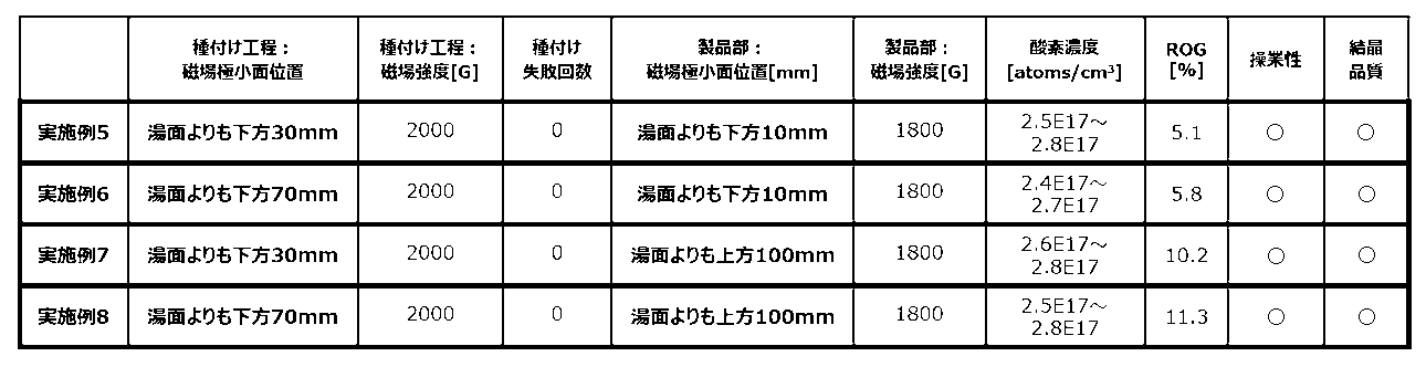
- Example 5-8 In Example 5-8, the magnetic field intensity in the seeding process was changed to 2000 G, the magnetic field intensity in the straight body process of the product part was changed to 1800 G, and the other conditions were the same as in Example 1-4. A single crystal was pulled under these conditions. Table 2 shows the results of Examples 5-8.
- Example 9-12 In Examples 9-12, the single crystal was pulled under a total of four types of pulling conditions, except that the magnetic field strength in the straight body process of the product section was changed to 750 G, and the other conditions were the same as in Examples 1-4. bottom. The results of Examples 9-12 are shown in Table 3.
- Examples 13-14 In Examples 13 and 14, a dislocation-free seeding method without a necking step (dash necking method) was carried out, and the other conditions were the same as in Examples 1 and 2. A total of two types of pulling conditions were used for unit pulling. Crystal pulling was performed. The results of Examples 13-14 are shown in Table 4.
- Comparative Example 1-4 In Comparative Example 1-4, the magnetic field minimum plane position during the seeding process was 0 mm below the molten metal surface or 15 mm below the molten metal surface, and the magnetic field strength at the intersection of the middle surface between the upper and lower coils and the inner wall of the crucible was 1500 G or 2000 G, Single crystals were pulled under a total of four types of pulling conditions, with the conditions of the straight body process of the product part being the same as the magnetic field minimum plane position and magnetic field intensity during the seeding process. In Comparative Examples 1-4, all other conditions were the same as those in Example 1. Table 5 shows the results of Comparative Examples 1-4.
- Comparative Example 5-6 In Comparative Example 5-6, a dislocation-free seeding method without a necking step (dash necking method) was performed, and the position of the magnetic field minimum plane during the seeding step was 0 mm below the melt surface or 15 mm below the melt surface, and the upper and lower coils.
- the magnetic field intensity at the intersection of the intermediate surface between the crucible and the inner wall of the crucible was 1500 G, and the conditions for the straight body process of the product part were the same as the magnetic minimum plane position and magnetic field intensity during the seeding process. Crystal pulling was performed. In Comparative Examples 5 and 6, all other conditions were the same as those in Example 1. Table 6 shows the results of Comparative Examples 5-6.
- a single crystal with a low oxygen concentration and a good in-plane distribution could be efficiently produced with an improved seeding success rate.
- the present invention is not limited to the above embodiments.
- the above-described embodiment is an example, and any device having substantially the same configuration as the technical idea described in the claims of the present invention and exhibiting the same effect is the present invention. included in the technical scope of
Landscapes
- Chemical & Material Sciences (AREA)
- Engineering & Computer Science (AREA)
- Crystallography & Structural Chemistry (AREA)
- Materials Engineering (AREA)
- Metallurgy (AREA)
- Organic Chemistry (AREA)
- Crystals, And After-Treatments Of Crystals (AREA)
Abstract
Description
まず、本発明に係るシリコン単結晶の製造方法に好適に使用される単結晶引上げ装置について説明する。図1に単結晶引上げ装置の一例を示す。図1に示す単結晶引上げ炉1は、断熱材9と、その内部の加熱ヒーター8と、黒鉛坩堝7内の石英坩堝6に収容されたシリコン融液5(原料融液)と対向するように熱遮蔽部材13が筒部12の下端に配置されている。また、周囲に設けられた上下2つの超電導コイルである上コイル30aと下コイル30bを有する磁場発生装置30とを備え、上コイル30a、下コイル30bに通電することによりシリコン融液5にカスプ磁場を印加する。引上げ炉1の中心軸10上であって、ワイヤーに接続された種ホルダ3で保持された種結晶2をシリコン融液5に接触させて種付けを行い、シリコン単結晶を拡径し、製品部となる直胴部を引上げ方向に引き上げてシリコン単結晶4を製造する構成となっている。
次に、本発明に係るシリコン単結晶の製造方法について説明する。本発明に係るシリコン単結晶の製造方法は、種結晶をシリコン融液に接触させて種付けを行う種付け工程と、シリコン単結晶を拡径した後に行われる直胴工程とを有している。種付け工程は、引上げ炉の中心軸上にある磁場極小面位置をシリコン融液の表面より下方の第1の位置として行い、直胴工程に移行する前に、引上げ炉の中心軸上にある磁場極小面位置を第1の位置より上方の第2の位置に移動させ、直胴工程は、引上げ炉の中心軸上にある磁場極小面位置を第2の位置として行う。以下、詳細に説明する。
種付け工程では単結晶引上げ炉1の中心軸10上にある磁場極小面位置31をシリコン融液5(原料融液)の表面よりも下方の第1の位置としてネッキング工程を実施する。このとき、種付け前には種結晶2をシリコン融液5の直上で5~60分程度加温することが好ましい。この加温を実施することで種結晶2とシリコン融液5の温度差が小さくなり、その結果として融液と種結晶が接触した際の熱ショックを緩和することができ、無転位でシリコン単結晶を引き上げる際の成功率がより向上し、生産性を向上することが可能となる。
種付け工程の後、直胴工程に移行する前に、単結晶引上げ炉1の中心軸10上にある磁場極小面位置31を第1の位置より上方の第2の位置に移動させ、直胴工程は、単結晶引上げ炉1の中心軸10上にある磁場極小面位置31を第2の位置として行う。これにより、低い酸素濃度でかつ良好な面内分布のシリコン単結晶を製造することが可能となる。
実施例1-4では、以下に示す条件でシリコン単結晶の製造を行った。
磁場極小面位置(=上下コイル間の0Gの位置):湯面から下方に30mm又は湯面から下方に70mm
上下コイル間の中間面と坩堝内壁の交点における磁場強度:1500G
坩堝回転速度:1.0rpm
単結晶回転速度:8rpm
磁場極小面位置:湯面から下方に10mm又は湯面から上方に100mm
上下コイル間の中間面と坩堝内壁の交点における磁場強度:1500G
坩堝回転速度:1.0rpm
単結晶回転速度:8rpm

実施例5-8では、種付け工程の磁場強度を2000G、製品部の直胴工程の磁場強度を1800Gに変更し、その他の条件は実施例1-4と同条件とした、合計4種類の引上げ条件で単結晶の引上げを実施した。実施例5-8の結果を表2に示す。
実施例9-12では、製品部の直胴工程の磁場強度のみ750Gに変更し、その他の条件は実施例1-4と同条件とした、合計4種類の引上げ条件で単結晶の引上げを実施した。実施例9-12の結果を表3に示す。

実施例13-14では、ネッキング工程(ダッシュネッキング法)を行わない無転位種付け法を実施し、その他の条件は実施例1、実施例2と同条件とした、合計2種類の引上げ条件で単結晶の引上げを実施した。実施例13-14の結果を表4に示す。

比較例1-4では、種付け工程中の磁場極小面位置を湯面から下方に0mm又は湯面から下方に15mm、上下コイル間の中間面と坩堝内壁の交点における磁場強度を1500G又は2000Gとし、製品部の直胴工程の条件は種付け工程中の磁場極小面位置及び磁場強度と同じ条件とした、合計4種類の引上げ条件で単結晶の引上げを実施した。なお、比較例1-4において、その他の条件は全て実施例1と同じ条件とした。比較例1-4の結果を表5に示す。

比較例5-6では、ネッキング工程(ダッシュネッキング法)を行わない無転位種付け法を実施し、種付け工程中の磁場極小面位置を湯面から下方に0mm又は湯面から下方に15mm、上下コイル間の中間面と坩堝内壁の交点における磁場強度を1500Gとし、製品部の直胴工程の条件は種付け工程中の磁場極小面位置及び磁場強度と同じ条件とした、合計2種類の引上げ条件で単結晶の引上げを実施した。なお、比較例5-6において、その他の条件は全て実施例1と同じ条件とした。比較例5-6の結果を表6に示す。

Claims (3)
- 引上げ炉に備えられた上側コイル及び下側コイルで形成するカスプ磁場を用いたCZ法によるシリコン単結晶の製造方法であって、
種結晶をシリコン融液に接触させて種付けを行う種付け工程と、シリコン単結晶を拡径した後に行われる直胴工程とを有し、
前記種付け工程は、前記引上げ炉の中心軸上にある磁場極小面位置を前記シリコン融液の表面より下方の第1の位置として行い、
前記直胴工程に移行する前に、前記引上げ炉の中心軸上にある磁場極小面位置を前記第1の位置より上方の第2の位置に移動させ、
前記直胴工程は、前記引上げ炉の中心軸上にある磁場極小面位置を前記第2の位置として行い、
前記第1の位置を、前記シリコン融液の表面から下方に30mm~80mmの位置とし、
前記第2の位置を、前記シリコン融液の表面から下方に10mm~上方に100mmの位置とし、
前記種付け工程において、前記上側コイル及び前記下側コイル間の中間面と坩堝内壁の交点における磁場強度を1500G以上とし、
前記直胴工程において、前記上側コイル及び前記下側コイル間の中間面と坩堝内壁の交点における磁場強度を750G以上、1800G以下とすることを特徴とするシリコン単結晶の製造方法。 - 前記種付け工程は無転位種付け法により行うことを特徴とする請求項1に記載のシリコン単結晶の製造方法。
- 前記種付け工程の後に、前記引上げ炉の中心軸上にある磁場極小面位置を前記シリコン融液の表面より下方の前記第1の位置としたままネッキング工程を行うことを特徴とする請求項1又は2に記載のシリコン単結晶の製造方法。
Priority Applications (4)
| Application Number | Priority Date | Filing Date | Title |
|---|---|---|---|
| US18/576,638 US20240328029A1 (en) | 2021-07-29 | 2022-07-28 | Method for producing silicon single crystal |
| KR1020247000285A KR20240038957A (ko) | 2021-07-29 | 2022-07-28 | 실리콘 단결정의 제조방법 |
| DE112022002697.9T DE112022002697B4 (de) | 2021-07-29 | 2022-07-28 | Verfahren zum herstellen eines silizium-einkristalls |
| CN202280046419.3A CN117597476A (zh) | 2021-07-29 | 2022-07-28 | 单晶硅的制造方法 |
Applications Claiming Priority (2)
| Application Number | Priority Date | Filing Date | Title |
|---|---|---|---|
| JP2021-124122 | 2021-07-29 | ||
| JP2021124122A JP7124938B1 (ja) | 2021-07-29 | 2021-07-29 | シリコン単結晶の製造方法 |
Publications (1)
| Publication Number | Publication Date |
|---|---|
| WO2023008508A1 true WO2023008508A1 (ja) | 2023-02-02 |
Family
ID=83004355
Family Applications (1)
| Application Number | Title | Priority Date | Filing Date |
|---|---|---|---|
| PCT/JP2022/029046 Ceased WO2023008508A1 (ja) | 2021-07-29 | 2022-07-28 | シリコン単結晶の製造方法 |
Country Status (6)
| Country | Link |
|---|---|
| US (1) | US20240328029A1 (ja) |
| JP (1) | JP7124938B1 (ja) |
| KR (1) | KR20240038957A (ja) |
| CN (1) | CN117597476A (ja) |
| DE (1) | DE112022002697B4 (ja) |
| WO (1) | WO2023008508A1 (ja) |
Families Citing this family (1)
| Publication number | Priority date | Publication date | Assignee | Title |
|---|---|---|---|---|
| JP7552942B1 (ja) | 2024-01-29 | 2024-09-18 | 信越半導体株式会社 | シリコン単結晶の抵抗率測定方法 |
Citations (12)
| Publication number | Priority date | Publication date | Assignee | Title |
|---|---|---|---|---|
| JPH107487A (ja) * | 1996-06-20 | 1998-01-13 | Komatsu Electron Metals Co Ltd | 磁場印加による半導体単結晶の製造方法 |
| JP2000239097A (ja) * | 1999-02-22 | 2000-09-05 | Sumitomo Metal Ind Ltd | 半導体用シリコン単結晶の引上げ方法 |
| JP2002249396A (ja) * | 2001-02-20 | 2002-09-06 | Sumitomo Metal Ind Ltd | シリコン単結晶の育成方法 |
| JP2002249397A (ja) * | 2001-02-16 | 2002-09-06 | Sumitomo Metal Ind Ltd | シリコン単結晶の製造方法 |
| JP2003002784A (ja) * | 2001-06-26 | 2003-01-08 | Sumitomo Mitsubishi Silicon Corp | シリコン単結晶の引上げ方法 |
| JP2007031187A (ja) * | 2005-07-25 | 2007-02-08 | Sumco Corp | シリコン単結晶製造方法及びシリコン単結晶 |
| JP2007145666A (ja) * | 2005-11-29 | 2007-06-14 | Toshiba Ceramics Co Ltd | シリコン単結晶の製造方法 |
| JP2008526666A (ja) * | 2004-12-30 | 2008-07-24 | エムイーエムシー・エレクトロニック・マテリアルズ・インコーポレイテッド | 成長するシリコン結晶のメルト−固体界面形状の可変磁界を用いる制御 |
| JP2012031005A (ja) * | 2010-07-30 | 2012-02-16 | Shin Etsu Handotai Co Ltd | シリコン単結晶の製造方法 |
| JP2013163642A (ja) * | 2013-05-28 | 2013-08-22 | Sumco Corp | シリコン単結晶の育成方法及びシリコンウェーハの製造方法 |
| JP2014227321A (ja) * | 2013-05-23 | 2014-12-08 | 信越半導体株式会社 | シリコン単結晶の製造方法 |
| JP2020033200A (ja) * | 2018-08-27 | 2020-03-05 | 株式会社Sumco | シリコン単結晶の製造方法及びシリコンウェーハ |
Family Cites Families (6)
| Publication number | Priority date | Publication date | Assignee | Title |
|---|---|---|---|---|
| JPH10273376A (ja) | 1997-03-29 | 1998-10-13 | Super Silicon Kenkyusho:Kk | 単結晶製造方法及び単結晶製造装置 |
| JP3750440B2 (ja) | 1999-09-22 | 2006-03-01 | 株式会社Sumco | 単結晶引上方法 |
| WO2003091483A1 (fr) | 2002-04-24 | 2003-11-06 | Shin-Etsu Handotai Co., Ltd. | Procede de production de silicium monocristallin, silicium monocristallin et plaquette de silicium |
| JP2009018984A (ja) | 2007-06-15 | 2009-01-29 | Covalent Materials Corp | 低酸素濃度シリコン単結晶およびその製造方法 |
| WO2009025340A1 (ja) | 2007-08-21 | 2009-02-26 | Sumco Corporation | Igbt用のシリコン単結晶ウェーハ及びigbt用のシリコン単結晶ウェーハの製造方法 |
| WO2019107190A1 (ja) | 2017-11-29 | 2019-06-06 | 株式会社Sumco | シリコン単結晶及びその製造方法並びにシリコンウェーハ |
-
2021
- 2021-07-29 JP JP2021124122A patent/JP7124938B1/ja active Active
-
2022
- 2022-07-28 US US18/576,638 patent/US20240328029A1/en active Pending
- 2022-07-28 KR KR1020247000285A patent/KR20240038957A/ko active Pending
- 2022-07-28 DE DE112022002697.9T patent/DE112022002697B4/de active Active
- 2022-07-28 WO PCT/JP2022/029046 patent/WO2023008508A1/ja not_active Ceased
- 2022-07-28 CN CN202280046419.3A patent/CN117597476A/zh active Pending
Patent Citations (12)
| Publication number | Priority date | Publication date | Assignee | Title |
|---|---|---|---|---|
| JPH107487A (ja) * | 1996-06-20 | 1998-01-13 | Komatsu Electron Metals Co Ltd | 磁場印加による半導体単結晶の製造方法 |
| JP2000239097A (ja) * | 1999-02-22 | 2000-09-05 | Sumitomo Metal Ind Ltd | 半導体用シリコン単結晶の引上げ方法 |
| JP2002249397A (ja) * | 2001-02-16 | 2002-09-06 | Sumitomo Metal Ind Ltd | シリコン単結晶の製造方法 |
| JP2002249396A (ja) * | 2001-02-20 | 2002-09-06 | Sumitomo Metal Ind Ltd | シリコン単結晶の育成方法 |
| JP2003002784A (ja) * | 2001-06-26 | 2003-01-08 | Sumitomo Mitsubishi Silicon Corp | シリコン単結晶の引上げ方法 |
| JP2008526666A (ja) * | 2004-12-30 | 2008-07-24 | エムイーエムシー・エレクトロニック・マテリアルズ・インコーポレイテッド | 成長するシリコン結晶のメルト−固体界面形状の可変磁界を用いる制御 |
| JP2007031187A (ja) * | 2005-07-25 | 2007-02-08 | Sumco Corp | シリコン単結晶製造方法及びシリコン単結晶 |
| JP2007145666A (ja) * | 2005-11-29 | 2007-06-14 | Toshiba Ceramics Co Ltd | シリコン単結晶の製造方法 |
| JP2012031005A (ja) * | 2010-07-30 | 2012-02-16 | Shin Etsu Handotai Co Ltd | シリコン単結晶の製造方法 |
| JP2014227321A (ja) * | 2013-05-23 | 2014-12-08 | 信越半導体株式会社 | シリコン単結晶の製造方法 |
| JP2013163642A (ja) * | 2013-05-28 | 2013-08-22 | Sumco Corp | シリコン単結晶の育成方法及びシリコンウェーハの製造方法 |
| JP2020033200A (ja) * | 2018-08-27 | 2020-03-05 | 株式会社Sumco | シリコン単結晶の製造方法及びシリコンウェーハ |
Also Published As
| Publication number | Publication date |
|---|---|
| CN117597476A (zh) | 2024-02-23 |
| DE112022002697T5 (de) | 2024-03-14 |
| DE112022002697B4 (de) | 2026-03-12 |
| JP7124938B1 (ja) | 2022-08-24 |
| US20240328029A1 (en) | 2024-10-03 |
| KR20240038957A (ko) | 2024-03-26 |
| JP2023019420A (ja) | 2023-02-09 |
Similar Documents
| Publication | Publication Date | Title |
|---|---|---|
| CN101133193B (zh) | 使用可变磁场控制生长的硅晶体的熔体-固体界面形状 | |
| JP5240191B2 (ja) | シリコン単結晶引上装置 | |
| EP2083098B1 (en) | Apparatus for manufacturing semiconductor single crystal ingot and method using the same | |
| JP2009114054A (ja) | 酸素濃度特性が改善した半導体単結晶の製造方法 | |
| JP2014509584A (ja) | 単結晶インゴットの製造方法およびこれによって製造された単結晶インゴットとウェハ | |
| JP5283543B2 (ja) | シリコン単結晶の育成方法 | |
| JP2011093778A (ja) | シリコン単結晶ウェーハおよびシリコン単結晶の製造方法 | |
| JP3601328B2 (ja) | シリコン単結晶の製造方法およびこの方法で製造されたシリコン単結晶とシリコンウエーハ | |
| JP7124938B1 (ja) | シリコン単結晶の製造方法 | |
| JP2018523626A (ja) | 単結晶インゴット成長装置及びその成長方法 | |
| CN118461131B (zh) | 用于拉制氧含量面内分布均匀的单晶衬底硅片的方法 | |
| JP2007031274A (ja) | シリコン単結晶インゴット、ウエハ、その成長装置、及びその成長方法 | |
| JP4461781B2 (ja) | シリコン単結晶の製造方法及びシリコン単結晶製造装置の設計方法並びにシリコン単結晶製造装置 | |
| JP2019196289A (ja) | 単結晶の製造方法及び単結晶引き上げ装置 | |
| JP7732403B2 (ja) | シリコン単結晶の製造方法 | |
| JP4293188B2 (ja) | 単結晶の製造方法及びシリコン単結晶ウエーハ | |
| JPH05208887A (ja) | Fz法シリコン単結晶棒の成長方法及び装置 | |
| JP5668786B2 (ja) | シリコン単結晶の育成方法及びシリコンウェーハの製造方法 | |
| JP4953386B2 (ja) | シリコン単結晶の引上げ方法 | |
| JP2000239096A (ja) | シリコン単結晶の製造方法 | |
| JP4150167B2 (ja) | シリコン単結晶の製造方法 | |
| JP4501507B2 (ja) | シリコン単結晶育成方法 | |
| JP7528799B2 (ja) | 単結晶引上げ装置および単結晶引上げ方法 | |
| WO2025134715A1 (ja) | 単結晶の製造方法 | |
| KR20170029948A (ko) | 단결정 잉곳 성장장치 및 그 성장방법 |
Legal Events
| Date | Code | Title | Description |
|---|---|---|---|
| 121 | Ep: the epo has been informed by wipo that ep was designated in this application |
Ref document number: 22849569 Country of ref document: EP Kind code of ref document: A1 |
|
| WWE | Wipo information: entry into national phase |
Ref document number: 202280046419.3 Country of ref document: CN |
|
| WWE | Wipo information: entry into national phase |
Ref document number: 18576638 Country of ref document: US |
|
| WWE | Wipo information: entry into national phase |
Ref document number: 112022002697 Country of ref document: DE |
|
| 122 | Ep: pct application non-entry in european phase |
Ref document number: 22849569 Country of ref document: EP Kind code of ref document: A1 |
|
| WWG | Wipo information: grant in national office |
Ref document number: 112022002697 Country of ref document: DE |