WO2023008308A1 - 半導体装置 - Google Patents
半導体装置 Download PDFInfo
- Publication number
- WO2023008308A1 WO2023008308A1 PCT/JP2022/028359 JP2022028359W WO2023008308A1 WO 2023008308 A1 WO2023008308 A1 WO 2023008308A1 JP 2022028359 W JP2022028359 W JP 2022028359W WO 2023008308 A1 WO2023008308 A1 WO 2023008308A1
- Authority
- WO
- WIPO (PCT)
- Prior art keywords
- layer
- barrier layer
- electrode
- semiconductor device
- field plate
- Prior art date
Links
- 239000004065 semiconductor Substances 0.000 title claims abstract description 204
- 230000004888 barrier function Effects 0.000 claims abstract description 258
- 150000004767 nitrides Chemical class 0.000 claims abstract description 84
- ATJFFYVFTNAWJD-UHFFFAOYSA-N Tin Chemical compound [Sn] ATJFFYVFTNAWJD-UHFFFAOYSA-N 0.000 claims abstract description 69
- 239000000758 substrate Substances 0.000 claims description 28
- 239000000463 material Substances 0.000 claims description 27
- QVGXLLKOCUKJST-UHFFFAOYSA-N atomic oxygen Chemical compound [O] QVGXLLKOCUKJST-UHFFFAOYSA-N 0.000 claims description 4
- 229910052760 oxygen Inorganic materials 0.000 claims description 4
- 239000001301 oxygen Substances 0.000 claims description 4
- 239000010410 layer Substances 0.000 description 686
- 229910052718 tin Inorganic materials 0.000 description 67
- 238000000034 method Methods 0.000 description 56
- 229910052751 metal Inorganic materials 0.000 description 32
- 239000002184 metal Substances 0.000 description 32
- 238000004519 manufacturing process Methods 0.000 description 24
- FAPWRFPIFSIZLT-UHFFFAOYSA-M Sodium chloride Chemical group [Na+].[Cl-] FAPWRFPIFSIZLT-UHFFFAOYSA-M 0.000 description 18
- 238000001312 dry etching Methods 0.000 description 18
- 229910002601 GaN Inorganic materials 0.000 description 17
- JMASRVWKEDWRBT-UHFFFAOYSA-N Gallium nitride Chemical compound [Ga]#N JMASRVWKEDWRBT-UHFFFAOYSA-N 0.000 description 17
- 238000012986 modification Methods 0.000 description 16
- 230000004048 modification Effects 0.000 description 16
- 238000009792 diffusion process Methods 0.000 description 14
- 238000001459 lithography Methods 0.000 description 12
- 230000005533 two-dimensional electron gas Effects 0.000 description 12
- 239000013078 crystal Substances 0.000 description 11
- 238000004544 sputter deposition Methods 0.000 description 10
- 239000011780 sodium chloride Substances 0.000 description 8
- 229910052737 gold Inorganic materials 0.000 description 6
- 230000008018 melting Effects 0.000 description 6
- 238000002844 melting Methods 0.000 description 6
- 239000010936 titanium Substances 0.000 description 6
- 150000001875 compounds Chemical class 0.000 description 5
- 238000000059 patterning Methods 0.000 description 5
- 238000010586 diagram Methods 0.000 description 4
- 230000005684 electric field Effects 0.000 description 4
- 239000012535 impurity Substances 0.000 description 4
- 238000005268 plasma chemical vapour deposition Methods 0.000 description 4
- 229910052721 tungsten Inorganic materials 0.000 description 4
- 239000000470 constituent Substances 0.000 description 3
- 238000007796 conventional method Methods 0.000 description 3
- 229910052802 copper Inorganic materials 0.000 description 3
- 230000008569 process Effects 0.000 description 3
- 239000002356 single layer Substances 0.000 description 3
- VEXZGXHMUGYJMC-UHFFFAOYSA-N Hydrochloric acid Chemical compound Cl VEXZGXHMUGYJMC-UHFFFAOYSA-N 0.000 description 2
- 229910052782 aluminium Inorganic materials 0.000 description 2
- 238000000231 atomic layer deposition Methods 0.000 description 2
- 230000033228 biological regulation Effects 0.000 description 2
- 238000005229 chemical vapour deposition Methods 0.000 description 2
- 238000000151 deposition Methods 0.000 description 2
- 238000013461 design Methods 0.000 description 2
- 230000006866 deterioration Effects 0.000 description 2
- 230000000694 effects Effects 0.000 description 2
- 150000002366 halogen compounds Chemical class 0.000 description 2
- 238000009413 insulation Methods 0.000 description 2
- 229910003465 moissanite Inorganic materials 0.000 description 2
- 230000003647 oxidation Effects 0.000 description 2
- 238000007254 oxidation reaction Methods 0.000 description 2
- 238000007747 plating Methods 0.000 description 2
- 230000010287 polarization Effects 0.000 description 2
- 238000012545 processing Methods 0.000 description 2
- 229910010271 silicon carbide Inorganic materials 0.000 description 2
- 125000006850 spacer group Chemical group 0.000 description 2
- -1 AlGaN Chemical compound 0.000 description 1
- 229910017083 AlN Inorganic materials 0.000 description 1
- 229910004298 SiO 2 Inorganic materials 0.000 description 1
- 229910004166 TaN Inorganic materials 0.000 description 1
- NRTOMJZYCJJWKI-UHFFFAOYSA-N Titanium nitride Chemical compound [Ti]#N NRTOMJZYCJJWKI-UHFFFAOYSA-N 0.000 description 1
- RNQKDQAVIXDKAG-UHFFFAOYSA-N aluminum gallium Chemical compound [Al].[Ga] RNQKDQAVIXDKAG-UHFFFAOYSA-N 0.000 description 1
- 230000015572 biosynthetic process Effects 0.000 description 1
- 230000015556 catabolic process Effects 0.000 description 1
- 238000004891 communication Methods 0.000 description 1
- 230000007547 defect Effects 0.000 description 1
- 238000002474 experimental method Methods 0.000 description 1
- 239000007789 gas Substances 0.000 description 1
- 238000010438 heat treatment Methods 0.000 description 1
- 238000005468 ion implantation Methods 0.000 description 1
- 238000004518 low pressure chemical vapour deposition Methods 0.000 description 1
- 238000009832 plasma treatment Methods 0.000 description 1
- 230000009467 reduction Effects 0.000 description 1
- 229910052594 sapphire Inorganic materials 0.000 description 1
- 239000010980 sapphire Substances 0.000 description 1
- 229910052814 silicon oxide Inorganic materials 0.000 description 1
- 230000002269 spontaneous effect Effects 0.000 description 1
- 229910052715 tantalum Inorganic materials 0.000 description 1
- MZLGASXMSKOWSE-UHFFFAOYSA-N tantalum nitride Chemical compound [Ta]#N MZLGASXMSKOWSE-UHFFFAOYSA-N 0.000 description 1
- 229910052719 titanium Inorganic materials 0.000 description 1
- 238000007740 vapor deposition Methods 0.000 description 1
- 238000001039 wet etching Methods 0.000 description 1
Images


Classifications
-
- H—ELECTRICITY
- H01—ELECTRIC ELEMENTS
- H01L—SEMICONDUCTOR DEVICES NOT COVERED BY CLASS H10
- H01L21/00—Processes or apparatus adapted for the manufacture or treatment of semiconductor or solid state devices or of parts thereof
- H01L21/02—Manufacture or treatment of semiconductor devices or of parts thereof
- H01L21/04—Manufacture or treatment of semiconductor devices or of parts thereof the devices having potential barriers, e.g. a PN junction, depletion layer or carrier concentration layer
- H01L21/18—Manufacture or treatment of semiconductor devices or of parts thereof the devices having potential barriers, e.g. a PN junction, depletion layer or carrier concentration layer the devices having semiconductor bodies comprising elements of Group IV of the Periodic Table or AIIIBV compounds with or without impurities, e.g. doping materials
- H01L21/28—Manufacture of electrodes on semiconductor bodies using processes or apparatus not provided for in groups H01L21/20 - H01L21/268
-
- H—ELECTRICITY
- H01—ELECTRIC ELEMENTS
- H01L—SEMICONDUCTOR DEVICES NOT COVERED BY CLASS H10
- H01L29/00—Semiconductor devices specially adapted for rectifying, amplifying, oscillating or switching and having potential barriers; Capacitors or resistors having potential barriers, e.g. a PN-junction depletion layer or carrier concentration layer; Details of semiconductor bodies or of electrodes thereof ; Multistep manufacturing processes therefor
- H01L29/40—Electrodes ; Multistep manufacturing processes therefor
- H01L29/41—Electrodes ; Multistep manufacturing processes therefor characterised by their shape, relative sizes or dispositions
- H01L29/417—Electrodes ; Multistep manufacturing processes therefor characterised by their shape, relative sizes or dispositions carrying the current to be rectified, amplified or switched
-
- H—ELECTRICITY
- H01—ELECTRIC ELEMENTS
- H01L—SEMICONDUCTOR DEVICES NOT COVERED BY CLASS H10
- H01L29/00—Semiconductor devices specially adapted for rectifying, amplifying, oscillating or switching and having potential barriers; Capacitors or resistors having potential barriers, e.g. a PN-junction depletion layer or carrier concentration layer; Details of semiconductor bodies or of electrodes thereof ; Multistep manufacturing processes therefor
- H01L29/66—Types of semiconductor device ; Multistep manufacturing processes therefor
- H01L29/66007—Multistep manufacturing processes
- H01L29/66075—Multistep manufacturing processes of devices having semiconductor bodies comprising group 14 or group 13/15 materials
- H01L29/66227—Multistep manufacturing processes of devices having semiconductor bodies comprising group 14 or group 13/15 materials the devices being controllable only by the electric current supplied or the electric potential applied, to an electrode which does not carry the current to be rectified, amplified or switched, e.g. three-terminal devices
- H01L29/66409—Unipolar field-effect transistors
- H01L29/66848—Unipolar field-effect transistors with a Schottky gate, i.e. MESFET
-
- H—ELECTRICITY
- H01—ELECTRIC ELEMENTS
- H01L—SEMICONDUCTOR DEVICES NOT COVERED BY CLASS H10
- H01L29/00—Semiconductor devices specially adapted for rectifying, amplifying, oscillating or switching and having potential barriers; Capacitors or resistors having potential barriers, e.g. a PN-junction depletion layer or carrier concentration layer; Details of semiconductor bodies or of electrodes thereof ; Multistep manufacturing processes therefor
- H01L29/66—Types of semiconductor device ; Multistep manufacturing processes therefor
- H01L29/68—Types of semiconductor device ; Multistep manufacturing processes therefor controllable by only the electric current supplied, or only the electric potential applied, to an electrode which does not carry the current to be rectified, amplified or switched
- H01L29/76—Unipolar devices, e.g. field effect transistors
- H01L29/772—Field effect transistors
- H01L29/778—Field effect transistors with two-dimensional charge carrier gas channel, e.g. HEMT ; with two-dimensional charge-carrier layer formed at a heterojunction interface
-
- H—ELECTRICITY
- H01—ELECTRIC ELEMENTS
- H01L—SEMICONDUCTOR DEVICES NOT COVERED BY CLASS H10
- H01L29/00—Semiconductor devices specially adapted for rectifying, amplifying, oscillating or switching and having potential barriers; Capacitors or resistors having potential barriers, e.g. a PN-junction depletion layer or carrier concentration layer; Details of semiconductor bodies or of electrodes thereof ; Multistep manufacturing processes therefor
- H01L29/66—Types of semiconductor device ; Multistep manufacturing processes therefor
- H01L29/68—Types of semiconductor device ; Multistep manufacturing processes therefor controllable by only the electric current supplied, or only the electric potential applied, to an electrode which does not carry the current to be rectified, amplified or switched
- H01L29/76—Unipolar devices, e.g. field effect transistors
- H01L29/772—Field effect transistors
- H01L29/80—Field effect transistors with field effect produced by a PN or other rectifying junction gate, i.e. potential-jump barrier
- H01L29/812—Field effect transistors with field effect produced by a PN or other rectifying junction gate, i.e. potential-jump barrier with a Schottky gate
Definitions
- the present disclosure relates to a semiconductor device, and more particularly to a group III nitride semiconductor device using a group III nitride semiconductor.
- Group III nitride semiconductors particularly group III nitride semiconductor devices using gallium nitride (GaN) or aluminum gallium nitride (AlGaN), have a high breakdown voltage due to the wide bandgap of the material.
- GaN gallium nitride
- AlGaN aluminum gallium nitride
- heterostructures such as AlGaN/GaN are easily formed in III-nitride semiconductor devices.
- a high concentration of electrons (hereinafter referred to as a two-dimensional electron gas layer) is generated on the GaN layer side of the AlGaN/GaN interface due to piezoelectric polarization generated from the lattice constant difference between materials and spontaneous polarization of AlGaN and GaN. ) are formed.
- the III-nitride semiconductor device utilizing the channel of the two-dimensional electron gas layer has a relatively high electron saturation velocity, a relatively high insulation resistance, and a relatively high thermal conductivity. applied to Then, it is necessary to use an electrode that is Schottky-junctioned to AlGaN as a gate electrode.
- the gate electrode In order to improve the characteristics of these III-nitride semiconductor devices, it is necessary for the gate electrode to reduce deterioration of the electrode during high-temperature operation and to reduce reverse leakage current. Therefore, it is preferable to use a material with a high melting point and a high work function as the material used for the gate electrode. By using this material, the heat resistance of the gate electrode and the height of the Schottky barrier should be increased as much as possible. In this way, deterioration of the electrode and reverse leakage current during high-temperature operation are reduced, thereby increasing reliability.
- a tantalum nitride (TaN ) layer, and the n-type GaN layer and the TaN layer form a Schottky junction.
- TaN with an N/Ta ratio of 1.00 in the NaCl structure not only has a high work function of 5.4 eV as a material, but also has a small difference in lattice constant in the a-axis direction from the n-type GaN layer.
- the work function is maximized, ie the Schottky barrier is maximized. Therefore, the heat resistance is high, the Schottky barrier can be increased, and a highly reliable gate electrode can be obtained.
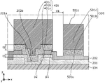
- FIG. 29 is a cross-sectional view showing the configuration in the vicinity of the gate electrode of the semiconductor device (III-nitride semiconductor device) according to Patent Document 2.
- FIG. 29 As shown in FIG. 29, in the semiconductor device according to Patent Document 2, a buffer layer 102, a GaN layer 103a, and an AlGaN layer 104a are provided on a substrate 101 in this order.
- This semiconductor device has a two-dimensional electron gas layer 105 on the GaN layer 103a side due to the heterostructure.
- a first insulating layer 211 is provided on the AlGaN layer 104a, and a first opening 211a is provided in the first insulating layer 211 by removing the first insulating layer 211 so as to expose the AlGaN layer 104a.
- a gate insulating layer 204 provided to cover the first insulating layer 211 and the first opening 211a, and a TaN layer 411a on the gate insulating layer 204 to cover the first opening 211a.
- a second insulating layer 212 is provided to cover the gate insulating layer 204 and the TaN layer 411a.
- a removed second opening 212b is provided.
- a titanium nitride layer (TiN layer 411b) and a first wiring layer 411c are laminated in this order so as to cover the second opening 212b. and a gate electrode 411 made of a layer 411c.
- the semiconductor device according to Patent Document 2 has a MIS (Metal-Insulator-Semiconductor) structure including the gate insulating layer 204, it may be used as an MES (MEtal-Semiconductor) structure.
- MES Metal-Insulator-Semiconductor
- the heat resistance is high and the Schottky barrier is high as described in Patent Document 1. can be obtained, and a highly reliable gate electrode can be obtained.
- JP 2006-190749 A Japanese Unexamined Patent Application Publication No. 2013-201370
- the gate electrode 411 is composed of a TaN layer 411a, a TiN layer 411b, and a first wiring layer 411c.
- levels are generated when metal atoms of the first wiring layer 411c diffuse into the AlGaN layer 104a or the first insulating layer 211 due to thermal history during the manufacturing process.
- the generated level lowers the Schottky barrier height, or traps electrons due to current collapse when a high voltage is applied between the source electrode and the drain electrode, increasing the on-resistance. Therefore, even if a temperature of about 250° C. to 500° C.
- the present disclosure has been made in view of such problems, and aims to provide a semiconductor device having a gate electrode with high reliability and low on-resistance.
- one aspect of the semiconductor device is a substrate, a first nitride semiconductor layer provided over the substrate, and a bandgap larger than that of the first nitride semiconductor layer.
- a second nitride semiconductor layer provided on the first nitride semiconductor layer, and a first insulating layer provided on the second nitride semiconductor layer are spaced apart from each other, Between the source electrode and the drain electrode electrically connected to the first nitride semiconductor layer through the insulating layer and the source electrode and the drain electrode, a first insulation layer is formed so that the second nitride semiconductor layer is exposed.
- the gate electrode being made of TaN; a first barrier layer having a layer thickness of Z1 and being in Schottky junction with the second nitride semiconductor layer; 2 barrier layers and a wiring layer provided on and in contact with the second barrier layer, Z1 and Z2 satisfy 200 nm ⁇ Z1+Z2 ⁇ 50 nm and Z1 ⁇ Z2 and 50 nm>Z1>3 nm.
- the semiconductor device According to the semiconductor device according to the present disclosure, it is possible to obtain a semiconductor device having a gate electrode with high reliability and low on-resistance.
- FIG. 1 is a cross-sectional view showing the configuration of the semiconductor device according to the first embodiment.
- FIG. 2 is a cross-sectional view showing an enlarged area II of FIG.
- FIG. 3 is a cross-sectional view showing the vicinity of a gate electrode included in a semiconductor device according to a study example of Embodiment 1.
- FIG. FIG. 4 is a graph showing the layer thickness dependence of the TiN layer of the reverse leakage current of the gate electrode and the on-resistance at high voltage/on-resistance at low voltage in the semiconductor device according to the study example of the first embodiment. is.
- FIG. 1 is a cross-sectional view showing the configuration of the semiconductor device according to the first embodiment.
- FIG. 2 is a cross-sectional view showing an enlarged area II of FIG.
- FIG. 3 is a cross-sectional view showing the vicinity of a gate electrode included in a semiconductor device according to a study example of Embodiment 1.
- FIG. FIG. 4 is a graph showing the layer
- FIG. 5 shows the layer thickness dependence results of the TiN layer of the reverse leakage current of the gate electrode and the on-resistance at high voltage/on-resistance at low voltage in the semiconductor device according to the study example of the first embodiment.
- is a diagram. 6A to 6D are cross-sectional views showing steps of the method for manufacturing the semiconductor device according to the first embodiment.
- 7A to 7D are cross-sectional views showing steps of the method for manufacturing the semiconductor device according to the first embodiment.
- FIG. 8 is a cross-sectional view showing steps of the method for manufacturing the semiconductor device according to the first embodiment.
- 9A to 9D are cross-sectional views showing steps of the method for manufacturing the semiconductor device according to the first embodiment.
- FIG. 10A and 10B are cross-sectional views showing steps of the method for manufacturing the semiconductor device according to the first embodiment.
- 11A and 11B are cross-sectional views showing steps of the method for manufacturing the semiconductor device according to the first embodiment.
- 12A and 12B are cross-sectional views showing steps of the method for manufacturing the semiconductor device according to the first embodiment.
- 13A and 13B are cross-sectional views showing steps of the method for manufacturing the semiconductor device according to the first embodiment.
- FIG. 14 is a cross-sectional view of the semiconductor device according to the second embodiment.
- 15 is a cross-sectional view showing a configuration in the vicinity of a gate electrode of a semiconductor device of Modification 1 according to Embodiment 2.
- FIG. 16 is a cross-sectional view showing a configuration in the vicinity of a gate electrode of a semiconductor device according to Modification 2 of Embodiment 2.
- FIG. 17 is a cross-sectional view showing a configuration in the vicinity of a gate electrode of a semiconductor device according to Modification 3 of Embodiment 2.
- FIG. 18 is a cross-sectional view showing an enlarged region XVIII in FIG. 17.
- FIG. 19 is a cross-sectional view showing a configuration in the vicinity of a gate electrode of a semiconductor device according to Modification 4 of Embodiment 2.
- FIG. 20A to 20C are cross-sectional views showing steps of the method for manufacturing a semiconductor device according to the second embodiment.
- 21A to 21C are cross-sectional views showing steps of the method for manufacturing a semiconductor device according to the second embodiment.
- 22A to 22C are cross-sectional views showing steps of the method for manufacturing a semiconductor device according to the second embodiment.
- 23A and 23B are cross-sectional views showing steps of the method for manufacturing the semiconductor device according to the second embodiment.
- 24A and 24B are cross-sectional views showing steps of the method for manufacturing a semiconductor device according to the second embodiment.
- 25A and 25B are cross-sectional views showing steps of the method for manufacturing the semiconductor device according to the second embodiment.
- 26A and 26B are cross-sectional views showing steps of the method for manufacturing the semiconductor device according to the second embodiment.
- 27A and 27B are cross-sectional views showing steps of the method for manufacturing the semiconductor device according to the second embodiment.
- 28A and 28B are cross-sectional views showing steps of the method for manufacturing the semiconductor device according to the second embodiment.
- FIG. 29 is a cross-sectional view showing the configuration near the gate electrode of
- the inventors conducted extensive studies and experiments to provide a semiconductor device having a gate electrode with high reliability and low on-resistance. As a result, the inventors came up with the following semiconductor device and the like.
- each figure is a schematic diagram and is not necessarily strictly illustrated.
- the same reference numerals are assigned to substantially the same configurations, and overlapping descriptions are omitted or simplified.
- top and bottom in the configuration of the semiconductor device do not refer to the upward direction (vertically upward) and the downward direction (vertically downward) in absolute spatial recognition, but to the stacked structure. It is a term defined by a relative positional relationship based on the stacking order in . Also, the terms “above” and “below” are used only when two components are spaced apart from each other and there is another component between the two components, as well as when two components are spaced apart from each other. It also applies when two components are in contact with each other and are placed in close contact with each other.
- the x-axis, y-axis and z-axis indicate three axes of a three-dimensional orthogonal coordinate system.
- the x-axis and y-axis are two axes parallel to the upper surface of the substrate of the semiconductor device, and the z-axis direction is perpendicular to the upper surface.
- the positive direction of the z-axis may be described as upward, and the negative direction of the z-axis may be described as downward.
- planar view refers to the substrate of the semiconductor device viewed from the z-axis positive direction.
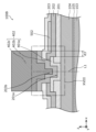
- FIG. 1 is a cross-sectional view showing the configuration of a semiconductor device 100A according to the first embodiment.
- FIG. 2 is a cross-sectional view showing an enlarged area II of FIG.
- HEMT high electron mobility transistor
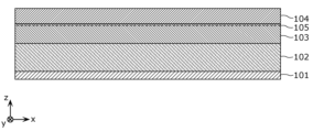
- a semiconductor device 100A includes a substrate 101, a buffer layer 102, a first nitride semiconductor layer 103, a second nitride semiconductor layer 104, a two-dimensional electron gas layer 105, and a first insulating layer.
- a source electrode 301 consisting of two wiring layers 301b, a drain electrode 302 consisting of an ohmic electrode 302a and a second wiring layer 302b, a first barrier layer 401a, a second barrier layer 401b and a wiring layer (first wiring layer 401c in this case). and a field plate electrode 501 composed of a third barrier layer 501b and a third wiring layer 501c.
- the substrate 101 is, for example, a substrate made of Si in the present embodiment.
- Substrate 101 is not limited to a substrate made of Si, and may be a substrate made of sapphire, SiC, GaN, AlN, or the like.
- the buffer layer 102 is provided on the substrate 101 .
- the buffer layer 102 is, for example, a group III nitride semiconductor layer having a layer thickness of 2 ⁇ m, and more specifically, a group III nitride semiconductor layer composed of a plurality of laminated structures composed of AlN and AlGaN. It is the material semiconductor layer.
- the layer thickness is the thickness of the layer in the z-axis direction.
- the buffer layer 102 may be composed of a single layer or multiple layers of a Group III nitride semiconductor such as GaN, AlGaN, AlN, InGaN, or AlInGaN.
- the first nitride semiconductor layer 103 is provided on the substrate 101 , more specifically, on the buffer layer 102 .
- the first nitride semiconductor layer 103 is made of GaN with a layer thickness of 200 nm, for example.
- the first nitride semiconductor layer 103 is not limited to GaN, and may be composed of a group III nitride semiconductor such as InGaN, AlGaN, or AlInGaN. It may contain n-type impurities.
- the second nitride semiconductor layer 104 has a larger bandgap than the first nitride semiconductor layer 103 and is provided on the first nitride semiconductor layer 103 .
- the second nitride semiconductor layer 104 is made of, for example, AlGaN with a layer thickness of 20 nm and an Al composition ratio of 25%.
- the Al composition ratio is 25% indicates that it is Al 0.25 Ga 0.75 N.
- a high-concentration two-dimensional electron gas is generated on the first nitride semiconductor layer 103 side of the heterointerface between the second nitride semiconductor layer 104 and the first nitride semiconductor layer 103, and the channel of the two-dimensional electron gas layer 105 is generated. is formed.
- the second nitride semiconductor layer 104 is not limited to AlGaN, and may be made of a group III nitride semiconductor such as AlInGaN.
- the second nitride semiconductor layer 104 contains n-type impurities. It may be
- a cap layer made of, for example, GaN and having a layer thickness of about 1 nm or more and 2 nm or less may be provided as a cap layer. That is, such a cap layer may be provided between the second nitride semiconductor layer 104 and the first insulating layer 201 . Further, as a spacer layer between the first nitride semiconductor layer 103 and the second nitride semiconductor layer 104, for example, a spacer layer made of AlN and having a layer thickness of about 1 nm may be provided.
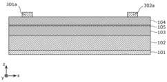
- the ohmic electrodes 301a and 302a are provided on the second nitride semiconductor layer 104 so as to face each other.
- each of the ohmic electrodes 301a and 302a is a multi-layered electrode film having a laminated structure in which a Ti film and an Al film are laminated in order, for example, but the present invention is not limited to this.
- the ohmic electrodes 301a and 302a are electrically ohmic-connected to the two-dimensional electron gas layer 105, respectively.
- recesses obtained by partially removing the second nitride semiconductor layer 104 and the first nitride semiconductor layer 103 and n-type impurities containing donors such as Si are provided. At least one of the contact layers may be provided. Also, the contact layer containing n-type impurities may be formed by plasma treatment, ion implantation, re-growth, and the like.
- the first insulating layer 201 is provided on the second nitride semiconductor layer 104 .
- first insulating layer 201 is provided to cover second nitride semiconductor layer 104, part of ohmic electrode 301a, and part of ohmic electrode 302a.
- the first insulating layer 201 is made of SiN with a layer thickness of 100 nm, for example.
- the first opening 201a is an example of an opening provided in the first insulating layer 201 between the source electrode 301 and the drain electrode 302 so that the second nitride semiconductor layer 104 is exposed.
- the first opening 201a is formed by removing the first insulating layer 201 between the ohmic electrodes 301a and 302a, and is provided so as to expose the second nitride semiconductor layer 104. It is
- the first barrier layer 401a covers the first opening 201a and part of the first insulating layer 201 so as to cover the portion of the second nitride semiconductor layer 104 and the first insulating layer 201 exposed through the first opening 201a. It is provided above the part.
- the layer thickness t1 of the first barrier layer 401a is assumed to be Z1.
- the first barrier layer 401a is, for example, a NaCl-type structure oriented only in the (111) plane having a layer thickness t1 (Z1) of 30 nm and an N/Ta ratio of 1.00. of TaN.
- the first barrier layer 401a and the second nitride semiconductor layer 104 are Schottky-junctioned. Z1 indicating the layer thickness t1 satisfies 50 nm>Z1>3 nm.
- Z1 is preferably Z1>10 nm because TaN has a NaCl structure oriented only in the (111) plane.
- the first barrier layer 401a may be TaN with an N/Ta ratio of 0.70 to 1.00 in a NaCl type structure oriented only in the (111) plane. By doing so, the Schottky barrier height can be increased as described in Patent Document 1.
- AlGaN has a lattice constant of 0.311 nm or more and 0.319 nm or less. Therefore, the difference in distance between atoms between the first barrier layer 401a made of TaN and the second nitride semiconductor layer 104 made of AlGaN can be reduced. Therefore, since dislocations are less likely to be formed in the first barrier layer 401a, diffusion of metal atoms of the first wiring layer 401c via dislocations in the first barrier layer 401a can be reduced.
- the second insulating layer 202 is provided to cover the first insulating layer 201 and the first barrier layer 401a. More specifically, the second insulating layer 202 is provided so as to cover the first insulating layer 201 and part of the first barrier layer 401a.
- the second insulating layer 202 is preferably composed of a material having an oxygen content of 1% or less, and is composed of SiN having a layer thickness of 150 nm, for example.
- the second insulating layer 202 is not limited to SiN, and may be SiC or SiCN.
- the second opening 202b is formed by removing the second insulating layer 202, and is provided so as to cover the range of the first opening 201a in plan view and to expose the first barrier layer 401a. ing.
- the first opening 201a is arranged so as to be included in the larger second opening 202b in plan view.
- the second opening 202b is provided so as to cover the range of the first opening 201a in plan view
- the end portion of the second opening 202b on the side of the drain electrode 302 is the first opening. It may be positioned inside the portion 201a. That is, in this case, in plan view, the size of the second opening 202b is smaller than that of the semiconductor device 100A shown in FIG. In this way, by reducing the size of the second opening 202b, which can be a path through which the metal atoms of the first wiring layer 401c diffuse, the first insulating layer 201 and the second nitride semiconductor layer 104 on the drain electrode 302 side are separated from each other. The diffusion of the metal atoms of the first wiring layer 401c into the can be further reduced.
- the second barrier layer 401b and the first wiring layer 401c are laminated in the order of the second barrier layer 401b and the first wiring layer 401c.
- the second barrier layer 401b is formed on the first barrier layer 401a exposed by the second opening 202b and part of the second insulating layer 202 so as to cover the second opening 202b. provided in contact.
- the first wiring layer 401c is provided on and in contact with the second barrier layer 401b.
- the first wiring layer 401c is an example of a wiring layer provided on and in contact with the second barrier layer 401b.
- the second barrier layer 401b is, for example, a layer made of TiN or WN with a layer thickness t2 (see FIG. 2) of 50 nm.
- the layer thickness t2 of the second barrier layer 401b is hereinafter referred to as Z2.
- the first wiring layer 401c is made of Al with a layer thickness of 450 nm, for example.
- the second barrier layer 401b is not limited to a single layer of TiN or WN, and may have a multilayer structure composed of TiN and WN.
- the first wiring layer 401c is not limited to Al, and may be W, Au, or Cu, or may be a compound containing these elements, or may be a plurality of laminated structures composed of these elements. It may be a multilayer electrode film consisting of.
- the distance (lattice constant) between adjacent metal atoms in the second barrier layer 401b made of TiN or WN oriented only in the (111) plane is about 0.302 nm or 0.298 nm, respectively.
- the distance (lattice constant) between adjacent metal atoms in the first barrier layer 401a made of TaN with an N/Ta ratio of 1.00 is 0.315 nm. Since the difference in the distance between adjacent metal atoms in the second barrier layer 401b and the first barrier layer 401a is thus small, dislocations are less likely to form in the second barrier layer 401b. Therefore, metal diffusion of metal atoms of the first wiring layer 401c through dislocations of the second barrier layer 401b is reduced.
- the crystal structure of the second barrier layer 401b is a NaCl type structure oriented only in the (111) plane
- the crystal structure of the first wiring layer 401c provided on the second barrier layer 401b is only the (111) plane. It becomes easy to have a crystal structure oriented to
- the first wiring layer 401c is composed of Al with a layer thickness of 450 nm
- the crystal structure of the first wiring layer 401c is an FCC type structure oriented only in the (111) plane, and the distance between adjacent metal atoms is 0.5. 286 nm. By doing so, the resistance of the first wiring layer 401c can be reduced and the reliability can be improved.
- the distance between adjacent metal atoms from the lower layer to the upper layer increases as in the first barrier layer 401a made of TaN, the second barrier layer 401b made of TiN or WN, and the first wiring layer 401c made of Al. Since the structure is such that it becomes smaller gradually, dislocations are less likely to be formed in the first wiring layer 401c. Therefore, the resistance of the first wiring layer 401c can be reduced and the reliability can be improved.
- the gate electrode 401 is an electrode including the first barrier layer 401a, the second barrier layer 401b and the first wiring layer 401c. Further, as shown in FIG. 1, the gate electrode 401 is an electrode provided spaced apart from the source electrode 301 and the drain electrode 302 and in contact with the second nitride semiconductor layer 104 at the first opening 201a. In other words, gate electrode 401 is an electrode that penetrates first insulating layer 201 and second insulating layer 202 and contacts second nitride semiconductor layer 104 .
- the first barrier layer 401a and the second barrier layer 401b branch from the first opening 201a on the way to the drain electrode 302 . More specifically, the first barrier layer 401a and the second barrier layer 401b branch at a branch point p2 indicated as a dashed circle in FIG.
- the direction from the first opening 201a toward the drain electrode 302 is the positive direction of the x-axis. That is, the first barrier layer 401a and the second barrier layer 401b are in contact with each other on the x-axis negative side of the branch point p2, and are separated from each other on the x-axis positive side of the branch point p2.
- the second insulating layer 202 is provided extending from above the first barrier layer 401a to above the first insulating layer 201 between the branch point p2 and the drain electrode 302 . That is, on the x-axis positive side of the branch point p2, part of the second insulating layer 202 is sandwiched between the first barrier layer 401a and the second barrier layer 401b.
- the field plate electrode 501 is an electrode provided on the second insulating layer 202 between the drain electrode 302 and the first opening 201a, which is an example of an opening.
- the third barrier layer 501b and the third wiring layer 501c forming the field plate electrode 501 are laminated in the order of the third barrier layer 501b and the third wiring layer 501c.
- the third barrier layer 501b is provided on part of the second insulating layer 202 between the second opening 202b and the drain electrode 302 .
- field plate electrode 501 comprising third barrier layer 501b and third interconnection layer 501c is formed.
- the field plate electrode 501 is connected to the potential of the source electrode 301 . In this case, field plate electrode 501 exhibits the same potential as source electrode 301 .
- the third barrier layer 501b preferably has the same configuration as the second barrier layer 401b, but is not limited to this. Also, the third wiring layer 501c may have the same configuration as the first wiring layer 401c, but the configuration is not limited to this.
- the uppermost surface position of the field plate electrode 501 is the second barrier layer closest to the drain electrode 302. It may be below the lower end position p1 of the side surface of 401b.
- the uppermost surface position of the field plate electrode 501 is the position of the uppermost surface 501t of the field plate electrode 501 shown in FIG.
- the side surface of the second barrier layer 401b is the surface of the second barrier layer 401b parallel to the yz plane, and the side surface closest to the drain electrode 302 is the side surface closest to the drain electrode 302. be.
- the lower end position p1 of the side surface of the second barrier layer 401b is indicated by a dashed circle.
- the position of the top surface 501t may be positioned below the lower end position p1 of the side surface of the second barrier layer 401b (negative z-axis side).
- the top surface position of field plate electrode 501 is located above lower end position p1 (z-axis positive side).
- the lowermost position of the field plate electrode 501 is provided below the lower end position p1 of the side surface of the second barrier layer 401b closest to the drain electrode 302. It is The lowermost surface position of the field plate electrode 501 is the position of the lowermost surface 501u of the field plate electrode 501 shown in FIG. In other words, in this case, as shown in FIG. 2, the position of the lowermost surface 501u is positioned below (z-axis negative side) the lower end position p1 of the side surface of the second barrier layer 401b. By doing so, the electric field at the lower end of the first barrier layer 401a closest to the drain electrode 302 can be further relaxed.
- the material of a part of the field plate electrode 501 is the same as the material of the second barrier layer 401b. More specifically, the material of the second barrier layer 401b and the material of the third barrier layer 501b are the same, and the material of the first wiring layer 401c and the material of the third wiring layer 501c are the same. By doing so, the gate electrode 401 and the field plate electrode 501 can be formed simultaneously.
- the field plate electrode 501 is composed of multiple layers including a lower layer and an upper layer. More specifically, the field plate electrode 501 is composed of a lower third barrier layer 501b and an upper third wiring layer 501c. As described above, the third barrier layer 501b and the third wiring layer 501c forming the field plate electrode 501 are made of the same material as the second barrier layer 401b and the first wiring layer 401c forming the gate electrode 401, respectively. Further, in this embodiment, the resistivity of the upper layer is lower than that of the lower layer. In other words, the resistivity of the third wiring layer 501c made of Al above the third barrier layer 501b made of TiN is small. Therefore, the impedance of the field plate electrode 501 can be lowered.
- the third opening 202c and the fourth opening 202d are formed by removing the first insulating layer 201 and the second insulating layer 202, and are provided so that the ohmic electrode 301a and the ohmic electrode 302a are partially exposed. It is
- the second wiring layer 301b is provided on the ohmic electrode 301a exposed by the third opening 202c and part of the second insulating layer 202 so as to cover the third opening 202c.
- the second wiring layer 302b is provided on the ohmic electrode 302a exposed through the fourth opening 202d and a portion of the second insulating layer 202 so as to cover the fourth opening 202d.
- each of the second wiring layer 301b and the second wiring layer 302b is configured by sequentially stacking TiN with a layer thickness of 200 nm, Al with a layer thickness of 3000 nm, and TiN with a layer thickness of 50 nm. be done.
- the second wiring layer 301b and the second wiring layer 302b are not limited to Al, and instead of Al, they may be Au or Cu, or compounds containing these elements. It may be a multilayer electrode film composed of a plurality of laminated structures.
- the source electrode 301 consisting of the ohmic electrode 301a and the second wiring layer 301b and the drain electrode 302 consisting of the ohmic electrode 302a and the second wiring layer 302b are constructed as described above. Also, the source electrode 301 and the drain electrode 302 are provided with a space therebetween.
- the source electrode 301 and the drain electrode 302 are electrically connected to the first nitride semiconductor layer 103 through the first insulating layer 201 and the second insulating layer 202 respectively. That is, in the present embodiment, the source electrode 301 and the drain electrode 302 are in contact with the second nitride semiconductor layer 104 at the third opening 202c and the fourth opening 202d, respectively. is electrically connected to
- Z1 indicating the layer thickness t1 of the first barrier layer 401a and Z2 indicating the layer thickness t2 of the second barrier layer 401b will be described. These Z1 and Z2 satisfy 200 nm ⁇ Z1+Z2 ⁇ 50 nm, Z1 ⁇ Z2 and 50 nm>Z1>3 nm.
- the semiconductor device 100A having the gate electrode 401 with high reliability and low on-resistance can be obtained.
- FIG. 3 is a cross-sectional view showing the vicinity of the gate electrode 401x included in the semiconductor device according to the study example of the first embodiment.
- the semiconductor device according to this examination example mainly does not have the second insulating layer 202, and the gate electrode 401x is configured by a laminated structure of a TiN layer 401bx and an Al layer 401cx. It has the same configuration as the semiconductor device 100A according to the embodiment.
- FIG. 4 shows the layer thickness dependence results of the TiN layer 401bx of the reverse leakage current of the gate electrode 401x and the on-resistance at high voltage/on-resistance at low voltage in the semiconductor device according to the study example of the first embodiment.
- FIG. 4 is a diagram showing; More specifically, the first axis (left axis) of the graph in FIG. 4 shows the result of the dependence of the reverse leakage current of the gate electrode 401x on the thickness of the TiN layer 401bx.
- the second axis (right axis) of the graph in FIG. 4 when a voltage is applied between the source electrode 301 and the drain electrode 302, which is an index of current collapse, and switching is performed, the voltage at high voltage (85 V) is shown.
- the results of the layer thickness dependence of the TiN layer 401bx for the ratio of the on-resistance to the on-resistance at low voltage (30 V) are shown.
- FIG. 5 shows the layer thickness dependence results of the TiN layer 401bx of the reverse leakage current of the gate electrode 401x and the on-resistance at high voltage/on-resistance at low voltage in the semiconductor device according to the study example of the first embodiment.
- Fig. 10 is another diagram showing; More specifically, the horizontal axis of the graph of FIG. 5 indicates the reverse leakage current of the gate electrode 401x, and the vertical axis of the graph of FIG. (30 V) shows the ratio to the on-resistance. Also, the layer thickness of the TiN layer 401bx is shown outside the frame.
- the dependence of the reverse leakage current of the gate electrode 401x on the thickness of the TiN layer 401bx shows that the reverse leakage current of the gate electrode 401x is reduced when the thickness of the TiN layer 401bx is 30 nm or more.
- the fluctuation of the reverse leakage current of the gate electrode 401x when the thickness of the TiN layer 401bx is 30 nm or more and 100 nm or less is sufficiently smaller than the fluctuation range when the thickness of the TiN layer 401bx is changed from 20 nm to 30 nm. Therefore, it is thought that this is due to manufacturing variations.
- the layer thickness dependence of the TiN layer 401bx for the ratio of the ON resistance at high voltage and at low voltage when switching when the layer thickness of the TiN layer 401bx is 50 nm or more and 100 nm or less, the ON resistance It can be seen that the resistance ratio becomes smaller and the current collapse is reduced. Furthermore, when the layer thickness of the TiN layer 401bx is 70 nm or more and 100 nm or less, the on-resistance ratio becomes even smaller and the current collapse is reduced.
- FIG. 5 shows a straight line with a downward sloping one-dot chain line, and it is shown that there is a trade-off relationship between the reduction of the reverse leakage current and the increase of the current collapse as the line gets closer to the straight line of the one-dot chain line. It is As shown in FIG. 5, as the thickness of the TiN layer 401bx increases to 50 nm, 70 nm, and 100 nm, the trade-off relationship disappears away from the downward-sloping chain line.
- the thickness of the TiN layer 401bx is 20 nm
- diffusion of the metal atoms of Al lowers the Schottky barrier, and it is thought that the reverse leakage current of the gate electrode 401x increases. Therefore, it is considered that the current collapse is reduced more than when the thickness of the TiN layer 401bx is 50 nm.
- the gate electrode 401 according to this embodiment is composed of a first barrier layer 401a (TaN), a second barrier layer 401b (TiN), and a first wiring layer 401c (Al).
- the gate electrode 401x according to the study example is composed of a TiN layer 401bx and an Al layer 401cx. That is, when part of the TiN layer 401bx according to the study example is replaced with the first barrier layer 401a, the gate electrode 401x according to the study example and the gate electrode 401 according to the present embodiment have the same configuration.
- TaN has a work function of 5.4 eV, a lattice constant of 0.310 nm or more and 0.315 nm or less, and a melting point of 3090°C.
- TiN has a work function of 4.7 eV, a lattice constant of 0.302 nm, and a melting point of 2930°C.
- the gate electrode 401 in which the TiN layer 401bx according to the study example is partially replaced with the first barrier layer 401a (TaN), the work function is increased compared to the gate electrode 401x according to the study example.
- the lattice constant and melting point are comparable. Therefore, if the layer thickness of the TiN layer 401bx and Z1+Z2 (the sum of the layer thickness of the first barrier layer 401a and the layer thickness of the second barrier layer 401b) are equivalent, the gate electrode 401 has It is expected that reverse leakage current is suppressed and current collapse is reduced.
- the first wiring layer 401c extends into the first insulating layer 201 and the second nitride semiconductor layer 104 by the first barrier layer 401a and the second barrier layer 401b. It is considered possible to suppress the diffusion of the metal atoms in the first insulating layer 201 and the second nitride semiconductor layer 104 to reduce the level. Therefore, it is possible to reduce the current collapse while reducing the reverse leakage current of the gate electrode 401 .
- the semiconductor device 100A having the gate electrode 401 with high reliability and low on-resistance can be obtained.
- WN has a work function of 4.6 eV and a lattice constant of 0.298 nm, which are values equivalent to those of TiN.
- WN has a melting point of less than 2000° C., which is sufficiently high. Therefore, the same effect can be expected when the second barrier layer 401b of the gate electrode 401 is made of WN instead of TiN.
- Z1+Z2 ⁇ 200 nm is preferable, Z1+Z2 ⁇ 150 nm is even better, and Z1+Z2 ⁇ 100 nm is even better.
- the first barrier layer 401a is made of TaN, which is a high melting point material, and the layer thickness t1 satisfies Z1>3 nm. Metal diffusion into the first insulating layer 201 and the second nitride semiconductor layer 104 can be suppressed more than when the barrier layer 401b is formed only.
- TaN is formed by a sputtering method, it grows in a discontinuous island shape in the initial stage of film formation, so Z1>3 nm tends to form a uniform film shape, so Z1>3 nm is preferable.
- Z1>10 nm is preferable, and Z1>15 nm is even better.
- Z1 indicating the layer thickness t1 of the first barrier layer 401a satisfies 50 nm>Z1.
- Z1 is better when 40 nm>Z1, and even better when Z1 is 30 nm>Z1.
- TaN forming the first barrier layer 401a exhibits high barrier properties, but has low workability by dry etching. Therefore, by making the layer thickness t1 of the first barrier layer 401a small, for example, 50 nm>Z1, the workability of the first barrier layer 401a can be improved.
- TaN must be processed by dry etching.
- dry etching since TaN has a high vapor pressure of a halogen compound, the selectivity between TaN and the first insulating layer 201 is low, and variations in the remaining film of the first insulating layer 201 increase. The variation in the remaining film of the first insulating layer 201 increases, and the variation in capacitance between the field plate electrode 501 and the drain electrode 302 increases.
- TiN or WN has a lower vapor pressure of a halogen compound than TaN, the selection ratio between TiN or WN and the first insulating layer 201 is high.
- the first wiring layer between the first insulating layer 201 and the second nitride semiconductor layer 104 is more likely to reach than the conventional technique of Patent Document 2. Diffusion of the metal atoms of 401c is suppressed, processing is facilitated, and therefore variations in residual film of the first insulating layer 201 are reduced. Therefore, the capacitance variation between the field plate electrode 501 and the drain electrode 302 can be reduced.
- the first barrier layer 401a made of TaN is covered with the first insulating layer 201 and the second insulating layer 202 made of SiN, and the second barrier layer 401b. Furthermore, the second insulating layer 202 is made of a material with an oxygen content of 1% or less. Therefore, oxidation of the first barrier layer 401a made of TaN is suppressed.
- 2 also shows the closest distance d1 between the gate electrode 401 and the field plate electrode 501.
- the closest distance d1 means the shortest distance between the gate electrode 401 and the field plate electrode 501.
- the closest distance d1 is the length in the x-axis direction in the cross-sectional view shown in FIG.
- the closest distance d1 is 100 nm or more. Also, the closest distance d1 is preferably 200 nm or more, more preferably 300 nm or more. By doing so, the ESD (Electrostatic Discharge) withstand voltage of the gate electrode 401 and the field plate electrode 501 can be sufficiently increased. Also, the closest distance d1 may be 1000 nm or less, preferably 900 nm or less, and even more preferably 800 nm or less. This facilitates downsizing of the semiconductor device 100A.
- a method for manufacturing the semiconductor device 100A according to the present embodiment will be described below with reference to FIGS.
- 6 to 13 are cross-sectional views showing steps of the method for manufacturing the semiconductor device 100A according to the first embodiment.
- a layered structure of AlN and AlGaN with a layer thickness of 2 ⁇ m is formed on a substrate 101 made of Si by using a metal organic chemical vapor deposition (MOCVD) method.
- MOCVD metal organic chemical vapor deposition
- the buffer layer 102, the first nitride semiconductor layer 103 having a thickness of 200 nm and made of GaN, and the second nitride semiconductor layer 104 having a thickness of 20 nm and having an Al composition ratio of 25% are arranged in the +c-plane direction ( ⁇ 0001> direction) are sequentially epitaxially grown.
- a high-concentration two-dimensional electron gas is generated on the first nitride semiconductor layer 103 side of the heterointerface between the second nitride semiconductor layer 104 and the first nitride semiconductor layer 103, forming a two-dimensional electron gas layer.
- 105 channels are formed.
- the second nitride semiconductor layer 104 is pre-cleaned with hydrochloric acid. Further, a mask is formed by applying a resist and then patterning the resist by lithography in areas other than the regions where the source electrode 301 and the drain electrode 302 are to be formed. Next, after a Ti film and an Al film are sequentially deposited by vapor deposition, ohmic electrodes 301a and 302a are formed by a lift-off method, as shown in FIG. Next, heat treatment is performed to electrically ohmic-connect the two-dimensional electron gas layer 105 and the ohmic electrodes 301a and 302a. The ohmic electrode 301a and the ohmic electrode 302a may be formed by sequentially applying the lithography method and the dry etching method after depositing the Ti film and the Al film by the sputtering method.
- a first insulating layer 201 made of SiN having a layer thickness of 100 nm is deposited by plasma CVD (Chemical Vapor Deposition). Thereafter, a mask is formed by applying a resist and then patterning the resist using a lithography method in areas other than the area where the gate electrode 401 is to be formed. Next, a dry etching method is used to form a first opening 201a so that the second nitride semiconductor layer 104 is exposed.
- the first insulating layer 201 may be SiCN, or may be SiN deposited by low pressure CVD.
- the wet etching method may be used to provide the first opening 201 a in the first insulating layer 201 .
- a sputtering apparatus is used to perform a sputtering process with a Ta target containing N2 gas, thereby depositing a first barrier layer 401a of TaN having a layer thickness of 30 nm. be.
- a resist is applied to the region where the gate electrode 401 is to be formed, and then the resist is patterned using a lithography method to form a mask.
- a dry etching method is then used to pattern the first barrier layer 401a.
- part of the first insulating layer 201 is removed by overetching, but since the thickness of the TaN (first barrier layer 401a) is as thin as 30 nm, the amount of removal of the first insulating layer 201 is minimized. , and variations in the remaining film of the first insulating layer 201 are reduced.
- a second insulating layer 202 of SiN having a layer thickness of 150 nm is deposited by plasma CVD. Thereafter, a mask is formed by applying a resist and then patterning the resist using a lithography method in areas other than the area where the gate electrode 401 is to be formed. Next, a dry etching method is used to form a second opening 202b to expose the first barrier layer 401a.
- TiN with a layer thickness of 50 nm and Al with a layer thickness of 450 nm are sequentially deposited by sputtering.
- TiN with a layer thickness of 50 nm corresponds to the second barrier layer 401b and the third barrier layer 501b
- Al with a layer thickness of 450 nm corresponds to the first wiring layer 401c and the third wiring layer 501c.
- a resist is applied to the regions where the gate electrode 401 and the field plate electrode 501 are to be formed, and then the resist is patterned using the lithography method to form a mask.
- the second barrier layer 401b and the third barrier layer 501b and the first wiring layer 401c and the third wiring layer 501c are patterned.
- gate electrode 401 and field plate electrode 501 are formed.
- a mask is formed by applying a resist and then patterning the resist using lithography in areas other than the regions where the source electrode 301 and the drain electrode 302 are to be formed.
- a dry etching method is used to form a third opening 202c and a fourth opening 202d to expose the ohmic electrode 301a and the ohmic electrode 302a.
- TiN with a layer thickness of 200 nm, Al with a layer thickness of 3000 nm, and TiN with a layer thickness of 50 nm are sequentially deposited by sputtering.
- a resist is applied to regions where the source electrode 301 and the drain electrode 302 are to be formed, and then the resist is patterned using a lithography method to form a mask.
- a dry etching method is used to pattern the second wiring layer 301b and the second wiring layer 302b.
- a source electrode 301 and a drain electrode 302 are formed.
- the second wiring layer 301b and the second wiring layer 302b may be formed not only by the dry etching method but also by the plating method or the damascene method. good too.
- the semiconductor device 100A formed as described above the first insulating layer 201 and the second nitride semiconductor layer 104 are separated from each other by the first barrier layer 401a and the second barrier layer 401b by satisfying 200 nm ⁇ Z1+Z2 ⁇ 50 nm. Diffusion of the metal atoms of the first wiring layer 401c into the inside is suppressed, and generation of levels in the first insulating layer 201 and the second nitride semiconductor layer 104 can be reduced. Therefore, it is possible to reduce the current collapse while reducing the reverse leakage current of the gate electrode 401 . Further, by setting Z1+Z2 ⁇ 70 nm, it is possible to further reduce the current collapse while reducing the reverse leakage current of the gate. Therefore, the semiconductor device 100A having the gate electrode 401 with high reliability and low on-resistance can be obtained.
- the first barrier layer 401a is made of TaN, which is a high-melting-point material, and the layer thickness t1 satisfies 50 nm>Z1>3 nm. Metal diffusion can be suppressed more than in the case of only two barrier layers 401b.
- Embodiment 2 a semiconductor device according to Embodiment 2 will be described with reference to FIG. 14 .
- FIG. 14 is a cross-sectional view showing the configuration of a semiconductor device 100B according to the second embodiment.
- the detailed description of the components common to the first embodiment is omitted.
- the semiconductor device 100B is a HEMT having a Schottky junction gate electrode.
- a semiconductor device 100B includes a substrate 101, a buffer layer 102, a first nitride semiconductor layer 103, a second nitride semiconductor layer 104, a two-dimensional electron gas layer 105, and a first insulating layer.
- Layer 201 opening (here, first opening 201a), second insulating layer 202, third insulating layer 203, second opening 203b, third opening 203c, and fourth opening 203d , a source electrode 301 consisting of an ohmic electrode 301a and a second wiring layer 301b, a drain electrode 302 consisting of an ohmic electrode 302a and a second wiring layer 302b, a first barrier layer 401a, a second barrier layer 402b and a wiring layer (here has a gate electrode 402 including a first wiring layer 402c) and a field plate electrode 502.
- a field plate electrode 502 is provided on the second insulating layer 202 between the gate electrode 402 and the drain electrode 302 . More specifically, field plate electrode 502 is an electrode provided on second insulating layer 202 between first opening 201a, which is an example of an opening, and drain electrode 302 . Also, the field plate electrode 502 is connected to the potential of the source electrode 301 . In this case, field plate electrode 502 exhibits the same potential as source electrode 301 . In this embodiment, the field plate electrode 502 is made of TiN with a layer thickness of 50 nm, for example. Note that the field plate electrode 502 is not limited to TiN, and may be composed of a plurality of layers including a lower layer and an upper layer.
- the resistivity of the upper layer may be lower than that of the lower layer.
- the field plate electrode 502 may be Al, Au, Cu, W, Ti, Ta, TiN, TaN, WN, Pt, etc., or a combination of compounds containing these elements.
- the third insulating layer 203 is provided so as to cover the second insulating layer 202 and the field plate electrode 502 . More specifically, the third insulating layer 203 is provided on the second insulating layer 202 between the branch point p2 and the drain electrode 302 so as to cover the field plate electrode 502 .
- the third insulating layer 203 is made of SiN with a layer thickness of 150 nm, for example.
- the second opening 203b is formed by removing the second insulating layer 202 and the third insulating layer 203, and covers the range of the first opening 201a in plan view, and the first barrier layer 401a. is exposed.
- the first opening 201a is arranged so as to be included in the larger second opening 203b in plan view.
- the second opening 203b is provided so as to cover the range of the first opening 201a in a plan view, but the end portion of the second opening 203b on the side of the drain electrode 302 is the first opening. It may be positioned inside the portion 201a. That is, in this case, the size of the second opening 203b is smaller in plan view than in the semiconductor device 100B shown in FIG.
- the size of the second opening 203b which can be a path through which the metal atoms of the first wiring layer 402c diffuse, the first insulating layer 201 and the second nitride semiconductor layer 104 on the drain electrode 302 side are separated from each other. The diffusion of the metal atoms of the first wiring layer 402c into the can be further reduced.
- the second barrier layer 402b and the first wiring layer 402c are laminated in the order of the second barrier layer 402b and the first wiring layer 402c.
- the second barrier layer 402b is formed on the first barrier layer 401a exposed by the second opening 203b and part of the third insulating layer 203 so as to cover the second opening 203b. provided in contact.
- the first wiring layer 402c is provided on and in contact with the second barrier layer 402b.
- the first wiring layer 402c is an example of a wiring layer provided on and in contact with the second barrier layer 402b.
- the second barrier layer 402b is made of TiN or WN with a layer thickness of 50 nm, for example.
- the first wiring layer 402c is made of Al with a layer thickness of 450 nm, for example.
- the second barrier layer 402b is not limited to a single layer of TiN or WN, and may have a multilayer structure composed of TiN and WN.
- the first wiring layer 402c is not limited to Al, but may be W, Au, or Cu, or may be a compound containing these elements, or may be a plurality of laminated structures composed of these elements. It may be a multilayer electrode film consisting of.
- the distance (lattice constant) between adjacent metal atoms in the second barrier layer 402b made of TiN or WN oriented only in the (111) plane is about 0.302 nm or 0.298 nm, respectively.
- the distance (lattice constant) between adjacent metal atoms in the first barrier layer 401a made of TaN with an N/Ta ratio of 1.00 is 0.315 nm.
- the crystal structure of the second barrier layer 402b is a NaCl type structure oriented only in the (111) plane, so that the crystal structure of the first wiring layer 402c provided on the second barrier layer 402b is only in the (111) plane. It becomes easy to have a crystal structure oriented to When the thickness of the first wiring layer 402c is 450 nm and the first wiring layer 402c is made of Al, the crystal structure of the first wiring layer 402c is an FCC type structure oriented only in the (111) plane, The distance between adjacent metal atoms is 0.286 nm. By doing so, the resistance of the first wiring layer 402c can be reduced and the reliability can be improved.
- the distance between adjacent metal atoms from the lower layer to the upper layer is large, such as the first barrier layer 401a made of TaN, the second barrier layer 402b made of TiN or WN, and the first wiring layer 402c made of Al. Since the structure is such that it becomes smaller gradually, dislocations are less likely to be formed in the first wiring layer 402c. Therefore, the resistance of the first wiring layer 402c can be further reduced and the reliability can be improved.
- the first barrier layer 401a and the second barrier layer 402b are branched from a branch point p2 on the way from the first opening 201a to the drain electrode 302. At this time, on the x-axis positive side of the branch point p2, the second insulating layer 202 and the third insulating layer 203 are sandwiched between the first barrier layer 401a and the second barrier layer 402b. More specifically, a part of the laminate composed of the second insulating layer 202 and the third insulating layer 203 is sandwiched between the first barrier layer 401a and the second barrier layer 402b.
- the top surface position of the field plate electrode 502 is provided below the lower end position p 1 of the side surface of the second barrier layer 402 b closest to the drain electrode 302 .
- the uppermost surface position of the field plate electrode 502 is the position of the uppermost surface 502t of the field plate electrode 502 shown in FIG.
- the side surface of the second barrier layer 402b is the surface of the second barrier layer 402b parallel to the yz plane, and the side surface closest to the drain electrode 302 is the side surface closest to the drain electrode 302. be.
- the lower end position p1 of the side surface of the second barrier layer 402b is indicated by a dashed circle.
- the position of the top surface 502t is located below the lower end position p1 of the side surface of the second barrier layer 402b (negative z-axis side).
- the area where the field plate electrode 502 and the gate electrode 402 face each other can be reduced, so that the capacitance between the field plate electrode 502 and the gate electrode 402 can be reduced.
- the first barrier layer 401a made of TaN is covered with the first insulating layer 201 and the second insulating layer 202 made of SiN, and the second barrier layer 402b. Furthermore, the second insulating layer 202 is made of a material with an oxygen content of 1% or less. Therefore, oxidation of the first barrier layer 401a made of TaN is suppressed.
- FIG. 14 also shows the closest distance d1 between the gate electrode 402 and the field plate electrode 502.
- the closest distance d1 means the shortest distance between the gate electrode 402 and the field plate electrode 502 .
- the closest distance d1 is the length in the x-axis direction in the cross-sectional view shown in FIG.
- the closest distance d1 is 100 nm or more. Also, the closest distance d1 is preferably 200 nm or more, more preferably 300 nm or more. By doing so, the ESD withstand voltage of the gate electrode 402 and the field plate electrode 502 can be sufficiently increased. Also, the closest distance d1 may be 1000 nm or less, preferably 900 nm or less, and even more preferably 800 nm or less. This facilitates compactness of the semiconductor device 100B.
- the lowermost surface position of the field plate electrode 502 is provided below the lower end position p1 of the side surface of the second barrier layer 402b closest to the drain electrode 302. It is The lowermost surface position of the field plate electrode 502 is the position of the lowermost surface 502u of the field plate electrode 502 shown in FIG. In other words, in this case, as shown in FIG. 14, the position of the lowermost surface 502u is positioned below (z-axis negative side) the lower end position p1 of the side surface of the second barrier layer 402b. By doing so, the electric field at the lower end of the first barrier layer 401a closest to the drain electrode 302 can be further relaxed.
- Third opening 203c and fourth opening 203d are formed by removing first insulating layer 201, second insulating layer 202, and third insulating layer 203, and are part of ohmic electrode 301a and ohmic electrode 302a. is exposed.
- the second wiring layer 301b is provided on the ohmic electrode 301a exposed by the third opening 203c and part of the third insulating layer 203 so as to cover the third opening 203c.
- the second wiring layer 302b is provided on the ohmic electrode 302a exposed through the fourth opening 203d and part of the third insulating layer 203 so as to cover the fourth opening 203d.
- the second wiring layer 301b and the second wiring layer 302b are each made of, for example, TiN with a layer thickness of 200 nm, Al with a layer thickness of 3000 nm, and TiN with a layer thickness of 50 nm.
- the second wiring layer 301b and the second wiring layer 302b are not limited to Al, and instead of Al, W, Au, or Cu may be used, or compounds containing these elements may be used. It may also be a multilayer electrode film composed of a plurality of laminated structures composed of elements.
- the semiconductor device 100B has the third insulating layer 203, and the second insulating layer 202 and the third insulating layer 203 are the first barrier layer 401a and the second barrier layer 402b. sandwiched between With the semiconductor device 100B having such a structure, the second insulating layer 202 and the third insulating layer 203 are designed independently, so that the structural design of the semiconductor device 100B is free from the viewpoint of ESD withstand voltage and electric field design. High degree. Furthermore, since the third insulating layer 203 is inserted between the first barrier layer 401a and the second barrier layer 402b, the electrostatic capacity between the field plate electrode 502 and the gate electrode 402 is small, the reliability is high, and the on-resistance is low. A gate electrode 402 having excellent characteristics is obtained.
- the dielectric constant of the material forming the third insulating layer 203 may be smaller than the dielectric constant of the material forming the second insulating layer 202 .
- the material forming the third insulating layer 203 may be, for example, SiO 2 , SiON, SiC, or SiCN, and may be selected according to the dielectric constant of the material forming the second insulating layer 202 . By doing so, the capacitance between the field plate electrode 502 and the gate electrode 402 can be reduced.
- the layer thickness of the second insulating layer 202 may be thinner than the layer thickness of the third insulating layer 203 . By doing so, the electric field can be relaxed at the end of the first barrier layer 401a on the drain electrode 302 side.
- At least one of the first barrier layer 401a and the second barrier layer 402b may be left-right asymmetric. That is, at least one of the shape of the first barrier layer 401a and the shape of the second barrier layer 402b is defined by a line of symmetry passing through the center of the opening (here, the first opening 201a) and parallel to the z-axis. It does not have to be symmetrical. By doing so, the degree of freedom in designing the structure of the field plate electrode 502 is improved.
- FIG. 15 Such a shape will be explained using FIGS. 15 to 19.
- FIG. 15 Such a shape will be explained using FIGS. 15 to 19.
- FIG. 15 is a cross-sectional view showing the configuration near the gate electrode 402 of the semiconductor device 100B of Modification 1 according to Embodiment 2. As shown in FIG.
- Semiconductor device 100B of Modification 1 according to Embodiment 2 is mainly except that field plate electrode 502 has a stepped shape and that second barrier layer 402b has a left-right asymmetric shape. , has the same configuration as the semiconductor device 100B according to the second embodiment.
- FIG. 15 a line of symmetry L1 passing through the center of the first opening 201a and parallel to the z-axis is shown.
- the shape of the second barrier layer 402b is not symmetrical with respect to the line of symmetry L1, for example, in the cross-sectional view shown in FIG. In this case, in the second barrier layer 402b, the extension length in the direction from the center of the first opening 201a toward the source electrode 301 and the extension length in the direction from the center toward the drain electrode 302 are different.
- the direction from the center toward the source electrode 301 is the negative direction of the x-axis
- the extension length in the negative direction of the x-axis is the length from the line of symmetry L1 to the end of the second barrier layer 402b on the source electrode 301 side. length.
- the direction from the center toward the source electrode 301 is the positive direction of the x-axis
- the extension length in the positive direction of the x-axis is the length from the line of symmetry L1 to the end of the second barrier layer 402b on the drain electrode 302 side. length.
- At least one of the first barrier layer 401a and the second barrier layer 402b (here, the second barrier layer 402b) has an extension length in the direction from the center of the first opening 201a toward the source electrode 301.
- the extension length in the direction from the center toward the drain electrode 302 is different. Thereby, the degree of freedom in designing the structure of the field plate electrode 502 is improved.
- the distance between the first barrier layer 401a and the field plate electrode 502 may be shorter than the distance d2 between the second barrier layer 402b and the field plate electrode 502. More specifically, the distance d2 between the second barrier layer 402b and the field plate electrode 502 is the length in the x-axis direction shown in FIG. Note that since the end of the first barrier layer 401a on the positive side of the x-axis and the end of the field plate electrode 502 on the negative side of the x-axis overlap in plan view, the distance between the first barrier layer 401a and the field plate electrode 502 is is 0 here. By doing so, the distance between the second barrier layer 402b and the drain electrode 302 is widened, so that the capacitance between the drain electrode 302 and the gate electrode 402 can be reduced.
- FIG. 16 is a cross-sectional view showing the configuration near the gate electrode 402 of the semiconductor device 100B of Modification 2 according to Embodiment 2. As shown in FIG.
- the semiconductor device 100B of Modification 2 of Embodiment 2 has the same configuration as the semiconductor device 100B of Modification 1 of Embodiment 2, except that the shape of the second barrier layer 402b is mainly different. .
- the shape of the second barrier layer 402b is not line-symmetrical about the line of symmetry L1, for example, in the cross-sectional view shown in FIG.
- the second barrier layer 402b is located on the x-axis negative side of the center of the first opening 201a (for example, the symmetry line L1) and on the x-axis positive side of the center of the first opening 201a (for example, the symmetry line L1).
- Each has a staircase shape.
- the stepped shape on the x-axis negative side from the center of the first opening 201a and the stepped shape on the x-axis positive side from the center of the first opening 201a have different numbers of steps.
- the distance between 401 a and field plate electrode 502 may be shorter than the distance d2 between second barrier layer 402 b and field plate electrode 502 . By doing so, the distance between the second barrier layer 402b and the drain electrode 302 is widened, so that the capacitance between the drain electrode 302 and the gate electrode 402 can be reduced.
- FIG. 17 is a cross-sectional view showing the configuration near the gate electrode 402 of the semiconductor device 100B of Modification 3 according to Embodiment 2. As shown in FIG. 18 is a cross-sectional view showing an enlarged region XVIII in FIG. 17.
- FIG. 18 is a cross-sectional view showing an enlarged region XVIII in FIG. 17.
- a semiconductor device 100B of Modified Example 3 according to Embodiment 2 has the same configuration as the semiconductor device 100B according to Embodiment 2, mainly except that the shape of the first barrier layer 401a is left-right asymmetric.
- the shape of the first barrier layer 401a is not symmetrical about the line of symmetry L1 in the cross-sectional views shown in FIGS. 17 and 18, for example. More specifically, in the first barrier layer 401a, the extension length in the direction from the center of the first opening 201a toward the source electrode 301 (hereinafter referred to as the first extension length) and the extension length in the direction from the center toward the drain electrode 302
- the stretched length (hereinafter referred to as the second stretched length) is different.
- the first stretch length and the second stretch length are length d4 and length d5, respectively.
- the first extension length is a length d4 along the x-axis negative direction, which is the direction from the center of the first opening 201a (for example, the line of symmetry L1) toward the source electrode 301.
- the extension length is a length d5 along the x-axis positive direction, which is the direction from the center of the first opening 201a (for example, the line of symmetry L1) toward the drain electrode 302 .
- the first stretching length and the second stretching length are length d6 and length d7, respectively.
- the first stretching length is the length d6 along the staircase-shaped step of the first barrier layer 401a located on the x-axis negative side of the line of symmetry L1
- the second stretching length is the length d6 along the line of symmetry.
- a length d7 is a length along the staircase-shaped step of the first barrier layer 401a located on the positive side of the x-axis from L1.
- the first stretched length and the second stretched length preferably satisfy length d4>length d5 or length d6>length d7. As shown in FIGS.
- the extension length (first extension length) from the center of the first opening 201a toward the source electrode 301 and the extension length from the center toward the drain electrode 302 It is different from the stretching length in the direction (second stretching length). Thereby, the degree of freedom in designing the structure of the field plate electrode 502 is improved.
- the distance d3 between the first barrier layer 401a and the field plate electrode 502 may be longer than the distance between the second barrier layer 402b and the field plate electrode 502. More specifically, the distance d3 between the first barrier layer 401a and the field plate electrode 502 is the length in the x-axis direction shown in FIG. Note that since the end of the second barrier layer 402b on the positive side of the x-axis and the end of the field plate electrode 502 on the negative side of the x-axis overlap in plan view, the distance between the second barrier layer 402b and the field plate electrode 502 is is 0 here.
- the widths of the second barrier layer 402b and the first wiring layer 402c are expanded toward the drain electrode 302, and the wiring resistance of the gate electrode 402 can be reduced. Furthermore, since the field plate electrode 502 has a flat shape, the capacitance between the field plate electrode 502 and the gate electrode 402 can be reduced.
- FIG. 19 is a cross-sectional view showing a configuration in the vicinity of a gate electrode 402 of a semiconductor device 100B of Modification 4 according to Embodiment 2. As shown in FIG.
- a semiconductor device 100B of Modification 4 of Embodiment 2 has the same configuration as semiconductor device 100B of Modification 3 of Embodiment 2, except that the shape of second barrier layer 402b is mainly different. .
- the distance d3 between the first barrier layer 401a and the field plate electrode 502 may be longer than the distance d2 between the second barrier layer 402b and the field plate electrode 502.
- the widths of the second barrier layer 402b and the first wiring layer 402c are further expanded toward the drain electrode 302, and the wiring resistance of the gate electrode 402 can be reduced.
- the capacitance between the field plate electrode 502 and the gate electrode 402 is increased. Therefore, by increasing the thickness of the third insulating layer 203, the structure can be designed so that the capacitance between the field plate electrode 502 and the gate electrode 402 does not increase.
- FIGS. 20 to 28 are cross-sectional views showing the configuration of the semiconductor device 100B during manufacturing.
- FIGS. 20 to 23 are the same as FIGS. 6 to 9 shown in Embodiment 1, detailed description thereof will be omitted.
- a second insulating layer 202 made of SiN having a thickness of 150 nm is deposited by plasma CVD, and then TiN having a thickness of 50 nm is successively deposited by sputtering.
- a resist is applied to the region where the field plate electrode 502 is to be formed, and the resist is patterned using a lithographic method to form a mask. A dry etching method is then used to form the field plate electrode 502 .
- a third insulating layer 203 of SiN having a layer thickness of 150 nm is deposited by plasma CVD. After that, a resist is applied to the area other than the area where the gate electrode 402 is to be formed, and then the resist is patterned using a lithography method to form a mask. Next, a dry etching method is used to form a second opening 203b to expose the first barrier layer 401a.
- a second barrier layer 402b made of TiN with a layer thickness of 50 nm and a first wiring layer 402c made of Al with a layer thickness of 450 nm are sequentially deposited by sputtering.
- a resist is applied to the region where the gate electrode 402 is to be formed, and then the resist is patterned using a lithography method to form a mask.
- a dry etching method is used to pattern the second barrier layer 402b and the first wiring layer 402c.
- the gate electrode 402 is formed.
- a mask is formed by applying a resist and then patterning the resist using lithography in areas other than the regions where the source electrode 301 and the drain electrode 302 are to be formed.
- a dry etching method is used to form a third opening 203c and a fourth opening 203d to expose the ohmic electrode 301a and the ohmic electrode 302a.
- TiN with a layer thickness of 200 nm, Al with a layer thickness of 3000 nm, and TiN with a layer thickness of 50 nm are sequentially deposited by sputtering.
- a resist is applied to regions where the source electrode 301 and the drain electrode 302 are to be formed, and then the resist is patterned using a lithography method to form a mask.
- a dry etching method is used to pattern the second wiring layer 301b and the second wiring layer 302b.
- a source electrode 301 and a drain electrode 302 are formed.
- the second wiring layer 301b and the second wiring layer 302b may be formed as wiring using Au or Cu by the plating method or the damascene method, not limited to the dry etching method.
- the semiconductor device 100B having the structure shown in FIG. 14 is completed through the series of steps described above.
- the semiconductor device 100B formed as described above since the opposing area between the field plate electrode 502 and the gate electrode 402 can be reduced, the capacitance between the field plate electrode 502 and the gate electrode 402 can be reduced. . Therefore, the semiconductor device 100B having the gate electrode 402 with small capacitance between the field plate electrode 502 and the gate electrode 402, high reliability, and low on-resistance is obtained.
- At least one of the first barrier layer 401a and the second barrier layer 402b may be bilaterally asymmetric.
- the distance between the first barrier layer 401a and the field plate electrode 502 may be shorter than the distance d2 between the second barrier layer 402b and the field plate electrode 502.
- the distance between first barrier layer 401a and field plate electrode 501 may be shorter than the distance between second barrier layer 401b and field plate electrode 501.
- the distance between the second barrier layer 401b and the drain electrode 302 is widened, so that the capacitance between the drain electrode 302 and the gate electrode 401 can be reduced.
- the distance d3 between the first barrier layer 401a and the field plate electrode 502 may be longer than the distance between the second barrier layer 402b and the field plate electrode 502.
- the distance between first barrier layer 401 a and field plate electrode 501 may be longer than the distance between second barrier layer 402 b and field plate electrode 501 .
- the width of the gate electrode 401 is expanded toward the drain electrode 302, and the wiring resistance of the gate electrode 401 can be reduced.
- the field plate electrode 501 has a flat shape, the capacitance between the field plate electrode 501 and the gate electrode 401 can be reduced.
- a semiconductor device is useful for communication equipment and inverters that require high-speed operation, power switching elements used in power supply circuits, and the like.
Landscapes
- Engineering & Computer Science (AREA)
- Microelectronics & Electronic Packaging (AREA)
- Power Engineering (AREA)
- Physics & Mathematics (AREA)
- Condensed Matter Physics & Semiconductors (AREA)
- General Physics & Mathematics (AREA)
- Computer Hardware Design (AREA)
- Ceramic Engineering (AREA)
- Manufacturing & Machinery (AREA)
- Junction Field-Effect Transistors (AREA)
Abstract
Description
まず、実施の形態1に係る半導体装置について、図1および図2を用いて説明する。図1は、実施の形態1に係る半導体装置100Aの構成を示す断面図である。図2は、図1の領域IIを拡大して示す断面図である。本実施の形態では、半導体装置100Aがショットキー接合ゲート構造を備えた高電子移動度トランジスタ(High Electron Mobility Transistor:HEMT)である場合について説明する。
ここで実施の形態2に係る半導体装置について、図14を用いて説明する。
以上、本開示に係る半導体装置について、各実施の形態に基づいて説明したが、本開示は、上記各実施の形態に限定されるものではない。
101 基板
102 バッファ層
103 第1窒化物半導体層
103a GaN層
104 第2窒化物半導体層
104a AlGaN層
105 二次元電子ガス層
201、211 第1絶縁層
201a、211a 第1開口部
202、212 第2絶縁層
202b、203b、212b 第2開口部
202c、203c 第3開口部
202d、203d 第4開口部
203 第3絶縁層
204 ゲート絶縁層
301 ソース電極
301a、302a オーミック電極
301b、302b 第2配線層
302 ドレイン電極
401、401x、402、411 ゲート電極
401a 第1バリア層
401b、402b 第2バリア層
401c、402c、411c 第1配線層
411a TaN層
401bx、411b TiN層
401cx Al層
501、502 フィールドプレート電極
501b 第3バリア層
501c 第3配線層
501t、502t 最上面
501u、502u 最下面
p1 下端位置
p2 分岐点
d1 最近接距離
d2、d3 間隔
d4、d5、d6、d7 長さ
L1 対称線
t1、t2 層厚
Claims (14)
- 基板と、
前記基板の上に設けられた第1窒化物半導体層と、
前記第1窒化物半導体層と比べてバンドギャップが大きく、前記第1窒化物半導体層の上に設けられた第2窒化物半導体層と、
前記第2窒化物半導体層の上に設けられた第1絶縁層と、
間隔を空けて設けられ、それぞれが前記第1絶縁層を貫通して前記第1窒化物半導体層に電気的に接続されたソース電極およびドレイン電極と、
前記ソース電極と前記ドレイン電極との間において、前記第2窒化物半導体層が露出するように前記第1絶縁層に設けられた開口部と、
前記ソース電極および前記ドレイン電極と間隔を空けて設けられ、前記開口部で前記第2窒化物半導体層に接触するゲート電極と、を有し、
前記ゲート電極は、
TaNからなり、層厚がZ1であり、前記第2窒化物半導体層にショットキー接合する第1バリア層と、
前記第1バリア層の上に接触して設けられ、TiNまたはWNからなり、層厚がZ2である第2バリア層と、
前記第2バリア層の上に接触して設けられた配線層と、を含み、
前記Z1および前記Z2は、200nm≧Z1+Z2≧50nm、Z1<Z2、および、50nm>Z1>3nmを満たす
半導体装置。 - 前記Z1および前記Z2は、Z1+Z2≧70nmを満たす
請求項1に記載の半導体装置。 - 前記Z1は、Z1>10nmを満たす
請求項1または2に記載の半導体装置。 - 前記第1バリア層と前記第2バリア層とは前記開口部から前記ドレイン電極に向かう途中の分岐点から分岐し、
前記半導体装置は、
前記分岐点と前記ドレイン電極との間の、前記第1バリア層の上から前記第1絶縁層の上に延伸して設けられた酸素含有率1%以下の第2絶縁層と、
前記開口部と前記ドレイン電極との間の、前記第2絶縁層の上に設けられた、前記ソース電極と同電位のフィールドプレート電極と、を有し、
前記フィールドプレート電極と前記ゲート電極との最近接距離は100nm以上1000nm以下である
請求項1~3のいずれか1項に記載の半導体装置。 - 前記基板が含む上面の垂直方向において、
前記フィールドプレート電極の最下面位置は、前記ドレイン電極に最近接する前記第2バリア層の側面の下端位置より下方である
請求項4に記載の半導体装置。 - 前記フィールドプレート電極の一部の材料は、前記第2バリア層の材料と同一である
請求項4または5に記載の半導体装置。 - 前記基板が含む上面の垂直方向において、
前記フィールドプレート電極の最上面位置は、前記ドレイン電極に最近接する前記第2バリア層の側面の下端位置より下方である
請求項4~6のいずれか1項に記載の半導体装置。 - 前記フィールドプレート電極は、下層と上層とを含む複数層で構成され、前記下層の抵抗率よりも前記上層の抵抗率が小さい
請求項4~7のいずれか1項に記載の半導体装置。 - 更に、前記分岐点と前記ドレイン電極との間の、前記第2絶縁層の上に、前記フィールドプレート電極を覆うように設けられた第3絶縁層を有し、
前記第2絶縁層と前記第3絶縁層とは、前記第1バリア層と前記第2バリア層とで挟まれている
請求項4~8のいずれか1項に記載の半導体装置。 - 前記第3絶縁層を構成する材料の誘電率は前記第2絶縁層を構成する材料の誘電率より小さい
請求項9に記載の半導体装置。 - 前記第2絶縁層の層厚は前記第3絶縁層の層厚より薄い
請求項9または10に記載の半導体装置。 - 前記第1バリア層と前記第2バリア層のうち少なくとも一方では、前記開口部の中央から前記ソース電極へ向かう方向への延伸長と前記中央から前記ドレイン電極へ向かう方向への延伸長とが異なる
請求項4~11のいずれか1項に記載の半導体装置。 - 前記基板の平面視において、
前記第1バリア層と前記フィールドプレート電極との間隔は、前記第2バリア層と前記フィールドプレート電極との間隔より短い
請求項12に記載の半導体装置。 - 前記基板の平面視において、
前記第1バリア層と前記フィールドプレート電極との間隔は、前記第2バリア層と前記フィールドプレート電極との間隔より長い
請求項12に記載の半導体装置。
Priority Applications (2)
| Application Number | Priority Date | Filing Date | Title |
|---|---|---|---|
| JP2023538480A JP7448728B2 (ja) | 2021-07-27 | 2022-07-21 | 半導体装置 |
| CN202280051723.7A CN117769762A (zh) | 2021-07-27 | 2022-07-21 | 半导体装置 |
Applications Claiming Priority (2)
| Application Number | Priority Date | Filing Date | Title |
|---|---|---|---|
| JP2021122144 | 2021-07-27 | ||
| JP2021-122144 | 2021-07-27 |
Publications (1)
| Publication Number | Publication Date |
|---|---|
| WO2023008308A1 true WO2023008308A1 (ja) | 2023-02-02 |
Family
ID=85086926
Family Applications (1)
| Application Number | Title | Priority Date | Filing Date |
|---|---|---|---|
| PCT/JP2022/028359 WO2023008308A1 (ja) | 2021-07-27 | 2022-07-21 | 半導体装置 |
Country Status (4)
| Country | Link |
|---|---|
| JP (1) | JP7448728B2 (ja) |
| CN (1) | CN117769762A (ja) |
| TW (1) | TW202306173A (ja) |
| WO (1) | WO2023008308A1 (ja) |
Citations (9)
| Publication number | Priority date | Publication date | Assignee | Title |
|---|---|---|---|---|
| JP2006190749A (ja) | 2005-01-05 | 2006-07-20 | Mitsubishi Electric Corp | 半導体素子および電界効果トランジスタ |
| JP2010517302A (ja) * | 2007-02-06 | 2010-05-20 | インターナショナル レクティフィアー コーポレイション | Iii族窒化物半導体デバイス |
| JP2010533987A (ja) * | 2007-07-20 | 2010-10-28 | アイメック | Iii−v族cmosデバイスでのダマシンコンタクト |
| JP2012523697A (ja) * | 2009-04-08 | 2012-10-04 | エフィシエント パワー コンヴァーション コーポレーション | エンハンスメントモードGaNHEMTデバイス、及びその製造方法 |
| JP2013201370A (ja) | 2012-03-26 | 2013-10-03 | Toshiba Corp | 窒化物半導体装置およびその製造方法 |
| US20140106516A1 (en) * | 2012-10-15 | 2014-04-17 | Infineon Technologies Austria Ag | Self-doped ohmic contacts for compound semiconductor devices |
| JP2014072388A (ja) * | 2012-09-28 | 2014-04-21 | Fujitsu Ltd | 化合物半導体装置及びその製造方法 |
| JP2014099523A (ja) * | 2012-11-15 | 2014-05-29 | Mitsubishi Electric Corp | ヘテロ接合電界効果型トランジスタおよびその製造方法 |
| US20200051823A1 (en) * | 2018-08-07 | 2020-02-13 | Stimicroelectronics S.R.L. | Method of manufacturing a hemt device with reduced gate leakage current, and hemt device |
Family Cites Families (5)
| Publication number | Priority date | Publication date | Assignee | Title |
|---|---|---|---|---|
| JP4547933B2 (ja) * | 2003-02-19 | 2010-09-22 | 日亜化学工業株式会社 | 窒化物半導体素子 |
| JP2008277640A (ja) * | 2007-05-02 | 2008-11-13 | Toshiba Corp | 窒化物半導体素子 |
| JP2008305816A (ja) * | 2007-06-05 | 2008-12-18 | Mitsubishi Electric Corp | 半導体装置及びその製造方法 |
| JP2013149851A (ja) * | 2012-01-20 | 2013-08-01 | Sharp Corp | 窒化物半導体装置 |
| JP6650867B2 (ja) * | 2016-12-22 | 2020-02-19 | 三菱電機株式会社 | ヘテロ接合電界効果型トランジスタの製造方法 |
-
2022
- 2022-07-21 WO PCT/JP2022/028359 patent/WO2023008308A1/ja active Application Filing
- 2022-07-21 JP JP2023538480A patent/JP7448728B2/ja active Active
- 2022-07-21 CN CN202280051723.7A patent/CN117769762A/zh active Pending
- 2022-07-22 TW TW111127569A patent/TW202306173A/zh unknown
Patent Citations (9)
| Publication number | Priority date | Publication date | Assignee | Title |
|---|---|---|---|---|
| JP2006190749A (ja) | 2005-01-05 | 2006-07-20 | Mitsubishi Electric Corp | 半導体素子および電界効果トランジスタ |
| JP2010517302A (ja) * | 2007-02-06 | 2010-05-20 | インターナショナル レクティフィアー コーポレイション | Iii族窒化物半導体デバイス |
| JP2010533987A (ja) * | 2007-07-20 | 2010-10-28 | アイメック | Iii−v族cmosデバイスでのダマシンコンタクト |
| JP2012523697A (ja) * | 2009-04-08 | 2012-10-04 | エフィシエント パワー コンヴァーション コーポレーション | エンハンスメントモードGaNHEMTデバイス、及びその製造方法 |
| JP2013201370A (ja) | 2012-03-26 | 2013-10-03 | Toshiba Corp | 窒化物半導体装置およびその製造方法 |
| JP2014072388A (ja) * | 2012-09-28 | 2014-04-21 | Fujitsu Ltd | 化合物半導体装置及びその製造方法 |
| US20140106516A1 (en) * | 2012-10-15 | 2014-04-17 | Infineon Technologies Austria Ag | Self-doped ohmic contacts for compound semiconductor devices |
| JP2014099523A (ja) * | 2012-11-15 | 2014-05-29 | Mitsubishi Electric Corp | ヘテロ接合電界効果型トランジスタおよびその製造方法 |
| US20200051823A1 (en) * | 2018-08-07 | 2020-02-13 | Stimicroelectronics S.R.L. | Method of manufacturing a hemt device with reduced gate leakage current, and hemt device |
Also Published As
| Publication number | Publication date |
|---|---|
| JP7448728B2 (ja) | 2024-03-12 |
| JPWO2023008308A1 (ja) | 2023-02-02 |
| CN117769762A (zh) | 2024-03-26 |
| TW202306173A (zh) | 2023-02-01 |
Similar Documents
| Publication | Publication Date | Title |
|---|---|---|
| TWI663698B (zh) | 半導體裝置 | |
| TWI770134B (zh) | 半導體裝置及半導體裝置之製造方法 | |
| US11417520B2 (en) | Semiconductor structure having sets of III-V compound layers and method of forming | |
| CN105938799B (zh) | 半导体器件的制造方法和半导体器件 | |
| US8207574B2 (en) | Semiconductor device and method for manufacturing the same | |
| US8525274B2 (en) | Semiconductor device and method of manufacturing the same | |
| TW201633532A (zh) | 半導體裝置及半導體裝置之製造方法 | |
| JP7082508B2 (ja) | 窒化物半導体装置 | |
| JP7065370B2 (ja) | 半導体デバイス及びその製造方法 | |
| JP5306438B2 (ja) | 電界効果トランジスタおよびその製造方法 | |
| JP2016149404A (ja) | 半導体装置の製造方法および半導体装置 | |
| TWI641133B (zh) | 半導體單元 | |
| TW201601312A (zh) | 半導體裝置及半導體裝置之製造方法 | |
| TW202103268A (zh) | 高電子遷移率電晶體及其製作方法 | |
| CN114556561B (zh) | 基于氮化物的半导体ic芯片及其制造方法 | |
| TW201635522A (zh) | 半導體單元 | |
| TW202238993A (zh) | 半導體結構 | |
| TWI725433B (zh) | 半導體裝置的製作方法 | |
| WO2023008308A1 (ja) | 半導体装置 | |
| JP6650867B2 (ja) | ヘテロ接合電界効果型トランジスタの製造方法 | |
| JP6176131B2 (ja) | 半導体装置の製造方法 | |
| TWI652820B (zh) | 半導體結構的製造方法及半導體裝置 | |
| JP2012227228A (ja) | 半導体デバイスおよび半導体デバイスの製造方法 | |
| JP4955858B2 (ja) | 多層構造半導体装置 | |
| TWI685970B (zh) | 半導體結構 |
Legal Events
| Date | Code | Title | Description |
|---|---|---|---|
| 121 | Ep: the epo has been informed by wipo that ep was designated in this application |
Ref document number: 22849370 Country of ref document: EP Kind code of ref document: A1 |
|
| WWE | Wipo information: entry into national phase |
Ref document number: 2023538480 Country of ref document: JP |
|
| WWE | Wipo information: entry into national phase |
Ref document number: 202280051723.7 Country of ref document: CN |
|
| WWE | Wipo information: entry into national phase |
Ref document number: 2022849370 Country of ref document: EP |
|
| NENP | Non-entry into the national phase |
Ref country code: DE |
|
| ENP | Entry into the national phase |
Ref document number: 2022849370 Country of ref document: EP Effective date: 20240227 |