WO2023008200A1 - 接合基板、回路基板及びその製造方法、並びに、個片基板及びその製造方法 - Google Patents
接合基板、回路基板及びその製造方法、並びに、個片基板及びその製造方法 Download PDFInfo
- Publication number
- WO2023008200A1 WO2023008200A1 PCT/JP2022/027620 JP2022027620W WO2023008200A1 WO 2023008200 A1 WO2023008200 A1 WO 2023008200A1 JP 2022027620 W JP2022027620 W JP 2022027620W WO 2023008200 A1 WO2023008200 A1 WO 2023008200A1
- Authority
- WO
- WIPO (PCT)
- Prior art keywords
- identification mark
- conductor
- circuit board
- dummy
- substrate
- Prior art date
- Legal status (The legal status is an assumption and is not a legal conclusion. Google has not performed a legal analysis and makes no representation as to the accuracy of the status listed.)
- Ceased
Links
Images




Classifications
-
- H—ELECTRICITY
- H05—ELECTRIC TECHNIQUES NOT OTHERWISE PROVIDED FOR
- H05K—PRINTED CIRCUITS; CASINGS OR CONSTRUCTIONAL DETAILS OF ELECTRIC APPARATUS; MANUFACTURE OF ASSEMBLAGES OF ELECTRICAL COMPONENTS
- H05K1/00—Printed circuits
- H05K1/02—Details
- H05K1/0266—Marks, test patterns or identification means
- H05K1/0269—Marks, test patterns or identification means for visual or optical inspection
-
- H—ELECTRICITY
- H05—ELECTRIC TECHNIQUES NOT OTHERWISE PROVIDED FOR
- H05K—PRINTED CIRCUITS; CASINGS OR CONSTRUCTIONAL DETAILS OF ELECTRIC APPARATUS; MANUFACTURE OF ASSEMBLAGES OF ELECTRICAL COMPONENTS
- H05K1/00—Printed circuits
- H05K1/02—Details
- H05K1/03—Use of materials for the substrate
- H05K1/0306—Inorganic insulating substrates, e.g. ceramic, glass
-
- H—ELECTRICITY
- H05—ELECTRIC TECHNIQUES NOT OTHERWISE PROVIDED FOR
- H05K—PRINTED CIRCUITS; CASINGS OR CONSTRUCTIONAL DETAILS OF ELECTRIC APPARATUS; MANUFACTURE OF ASSEMBLAGES OF ELECTRICAL COMPONENTS
- H05K2201/00—Indexing scheme relating to printed circuits covered by H05K1/00
- H05K2201/09—Shape and layout
- H05K2201/09209—Shape and layout details of conductors
- H05K2201/09654—Shape and layout details of conductors covering at least two types of conductors provided for in H05K2201/09218 - H05K2201/095
- H05K2201/09781—Dummy conductors, i.e. not used for normal transport of current; Dummy electrodes of components
-
- H—ELECTRICITY
- H05—ELECTRIC TECHNIQUES NOT OTHERWISE PROVIDED FOR
- H05K—PRINTED CIRCUITS; CASINGS OR CONSTRUCTIONAL DETAILS OF ELECTRIC APPARATUS; MANUFACTURE OF ASSEMBLAGES OF ELECTRICAL COMPONENTS
- H05K2201/00—Indexing scheme relating to printed circuits covered by H05K1/00
- H05K2201/09—Shape and layout
- H05K2201/09818—Shape or layout details not covered by a single group of H05K2201/09009 - H05K2201/09809
- H05K2201/09918—Optically detected marks used for aligning tool relative to the PCB, e.g. for mounting of components
-
- H—ELECTRICITY
- H05—ELECTRIC TECHNIQUES NOT OTHERWISE PROVIDED FOR
- H05K—PRINTED CIRCUITS; CASINGS OR CONSTRUCTIONAL DETAILS OF ELECTRIC APPARATUS; MANUFACTURE OF ASSEMBLAGES OF ELECTRICAL COMPONENTS
- H05K2203/00—Indexing scheme relating to apparatus or processes for manufacturing printed circuits covered by H05K3/00
- H05K2203/10—Using electric, magnetic and electromagnetic fields; Using laser light
- H05K2203/107—Using laser light
-
- H—ELECTRICITY
- H05—ELECTRIC TECHNIQUES NOT OTHERWISE PROVIDED FOR
- H05K—PRINTED CIRCUITS; CASINGS OR CONSTRUCTIONAL DETAILS OF ELECTRIC APPARATUS; MANUFACTURE OF ASSEMBLAGES OF ELECTRICAL COMPONENTS
- H05K3/00—Apparatus or processes for manufacturing printed circuits
- H05K3/0011—Working of insulating substrates or insulating layers
- H05K3/0044—Mechanical working of the substrate, e.g. drilling or punching
- H05K3/0052—Depaneling, i.e. dividing a panel into circuit boards; Working of the edges of circuit boards
Definitions
- the present disclosure relates to a bonded substrate, a circuit board and its manufacturing method, and an individual piece substrate and its manufacturing method.
- insulating ceramic substrates are used for individual substrates mounted on electronic devices.
- a multi-piece wiring board for obtaining such an individual board a plurality of wiring board regions are arranged vertically and horizontally, a dummy region is provided in the outer peripheral portion, and a symbol pattern consisting of voids is formed in the inner layer of each wiring board region.
- What is provided is known (for example, Patent Literature 1).
- a step of irradiating a part of a ceramic green sheet used as a material of the individual substrate with a laser beam to draw a bar code or a two-dimensional code, and firing the ceramic green sheet to form a plurality of substrate forming regions is known that includes a step of obtaining a ceramic substrate provided with the ceramic substrate and a step of dividing the ceramic substrate (for example, Patent Documents 2 and 3). This makes it possible to associate the molding lot number with the final product.
- Identification marks such as symbol patterns and two-dimensional codes as described in Patent Documents 1 to 3 are considered useful for traceability. Therefore, the present disclosure provides a circuit board with excellent traceability and a manufacturing method thereof. It also provides a bonded substrate with excellent traceability. Also provided is an individual substrate with excellent traceability and a method of manufacturing the same.
- a circuit board including a circuit forming portion and a dummy portion, comprising a ceramic plate and a plurality of conductors joined to the main surface of the ceramic plate, The plurality of conductor portions includes a first conductor portion provided in the dummy portion and a second conductor portion provided in the circuit formation portion, A circuit board having a first identification mark on the surface of the first conductor.
- a circuit board according to [1] wherein a part of the outer edge of the first conductor portion in the dummy portion surrounding the circuit forming portion protrudes outside the main surface of the ceramic plate.
- a bonded substrate comprising: a ceramic plate having a main surface including a circuit forming region and a dummy region; and a metal plate bonded to the ceramic plate so as to cover the main surface, wherein the metal plate is , the bonded substrate having a third identification mark on the surface of the portion covering the dummy region.
- a part of the outer edge of the metal plate protrudes outside the main surface of the ceramic plate, and corners of the ceramic plate protrude outside the metal plate.
- bonded substrate [8] having a fourth identification mark on the surface of the portion covering the circuit formation region, the fourth identification mark including fourth information related to the third information included in the third identification mark; [6] ] or the bonded substrate according to [7].
- the circuit board of [1] above by providing the first conductor portion having the first identification mark in the dummy portion, traceability can be ensured without providing the identification mark in the circuit forming portion. Further, since the first conductor has the first identification mark on the surface thereof, it is possible to improve the reading accuracy as compared with the case where the identification mark is provided inside the circuit board. Therefore, the circuit board has excellent traceability.
- the circuit board may have the configuration of [2].
- the circuit board may have the configuration of [3].
- the circuit board may have the configuration of [4]. Since such a circuit board has the second identification mark on the surface of the second conductor portion, the reading accuracy can be improved compared to the case where the identification mark is provided inside the circuit forming portion. In addition, since the second identification mark includes the second information related to the first information included in the first identification mark, the traceability of the circuit forming portion (individual board) obtained by separating the dummy portion from the circuit board is ensured. can also be ensured. Further, the circuit board and the circuit forming part (individual board) obtained by separating the dummy part from the circuit board can be linked and managed. Therefore, the scope of traceability can be extended.
- the circuit board may have the configuration of [5]. As a result, reading accuracy can be sufficiently maintained even if surface treatment is performed. Therefore, the reliability of traceability can be made sufficiently high.
- the bonded substrate of [6] above has the third identification mark on the surface of the metal plate, so it has excellent traceability. Further, since the metal plate has the third identification mark on the surface of the portion covering the dummy region, traceability can be ensured without providing the identification mark on the portion to be the circuit forming portion.
- the bonding substrate may have the configuration of [7]. Even if the main surfaces of the metal plate and the ceramic plate are joined via the brazing filler metal layer because part of the outer edge of the metal plate protrudes from the main surface of the ceramic plate, the brazing filler metal is not metal. It is possible to prevent the third identification mark from being covered with the third identification mark by seeping out to the surface of the plate. Therefore, it is possible to maintain sufficiently high reading accuracy of the third identification mark. In addition, since the corners of the ceramic plate are exposed, alignment can be performed using the corners. Such a bonded substrate, and circuit substrates and individual substrates obtained therefrom have excellent dimensional accuracy.
- the bonding substrate may have the configuration of [8]. This can extend the scope of traceability. For example, etching can be used to form a dummy portion and a circuit formation portion, and traceability can be ensured even after they are separated.
- the bonding substrate may have the configuration of [9]. This makes it possible to sufficiently maintain the reading accuracy of the identification mark derived from the third identification mark even after the bonding substrate is subjected to the surface treatment and the etching treatment. This makes it possible to sufficiently increase the reliability of traceability.
- the individual board of [10] above has a second identification mark on the surface of the second conductor portion.
- a second identification mark can improve reading accuracy compared to the case where the identification mark is provided inside the individual substrate.
- the second identification mark includes the second information related to the first information included in the first identification mark, it is possible to manage the circuit board or the dummy section and the individual circuit board in association with each other, The scope of traceability can be extended. Therefore, the individual substrates have excellent traceability.
- the individual board may have the configuration of [11]. As a result, reading accuracy can be improved and the reliability of traceability can be made sufficiently high.
- the joint board has the third identification mark on the surface of the metal plate, and the circuit board has the first identification mark derived from the third identification mark on the surface of the first conductor portion. have. Therefore, it is possible to ensure traceability from the bonding board to the circuit board. Further, since the first identification mark and the third identification mark are provided on the surfaces of the conductor portion and the metal plate, they are excellent in reading accuracy. Therefore, the circuit board manufacturing method is excellent in traceability.
- the bonded substrate has the third identification mark on the surface of the metal plate, and the circuit substrate has the first identification mark derived from the third identification mark on the surface of the first conductor. have Therefore, it is possible to ensure traceability from the bonding board to the circuit board. Also, the first identification mark and the third identification mark are excellent in reading accuracy. Therefore, the above-described method for manufacturing individual substrates is excellent in traceability.
- a circuit board with excellent traceability and its manufacturing method can be provided. Also, a bonded substrate with excellent traceability can be provided. Also, it is possible to provide an individual substrate with excellent traceability and a method for manufacturing the same.
- FIG. 1 is a perspective view of a bonded substrate according to one embodiment
- FIG. FIG. 4 is a diagram showing an example of an identification mark
- FIG. 2 is a cross-sectional view taken along line III-III of the bonding substrate of FIG. 1
- It is a top view of a ceramic board.
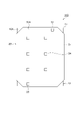
- 1 is a plan view of a circuit board according to one embodiment
- FIG. FIG. 6 is a sectional view of the circuit board of FIG. 5 taken along the line VI-VI
- FIG. 10 is a plan view of a bonded substrate according to another embodiment
- FIG. 4 is a plan view of a circuit board according to another embodiment
- 1 is a perspective view of an individual substrate according to one embodiment
- FIG. 1 is a perspective view of a bonding substrate 100 according to one embodiment.
- the bonded substrate 100 of FIG. 1 includes a ceramic plate 10 and a pair of metal plates 20 and 30 bonded to the ceramic plate 10 so as to cover both main surfaces of the ceramic plate 10, respectively.
- the pair of metal plates 20, 30 may be, for example, copper plates or aluminum plates.
- the bonding substrate 100 has a third identification mark 23 on the surface 20A of the metal plate 20 .
- the surface of the metal plate 30 may or may not have a similar identification mark. Although two third identification marks 23 are shown on the surface 20A, the number is not limited and may be one or three or more.
- the third identification mark 23 may be any mark that can identify the metal plate 20 and the bonding substrate 100 .
- it may be a one-dimensional code such as a bar code, or a two-dimensional code.
- the third identification mark 23 may be printed on the front surface 20A, or may be configured in an uneven shape. For example, it may be a combination of recesses and patterns.
- the plurality of third identification marks 23 may be the same or different.
- the third identification mark 23 is configured to be detectable by an imaging device such as a camera or video, for example.
- the imaging device may include, for example, an information processing section that compares the captured image with pre-recorded information and outputs information based on the comparison result.
- Other identifying marks in this disclosure may be similar.
- the third identification mark 23 may be used to identify the joint board 100 and the circuit board 200 which will be described later. In addition, if it is provided on the surfaces of the metal plates 20 and 30 before manufacturing the bonding substrate 100, the metal plates 20 and 30 can be identified.
- the third identification mark 23 may be a code associated with some information. The information includes, for example, lot, manufacturing history, product type, application, quality, and manufacturing conditions. By using the third identification mark 23, the traceability of the metal plates 20, 30, the bonded substrate 100, and various products obtained therefrom can be improved. For example, the third identification mark 23 may be used for quality control and process control.
- the third identification mark 23 is, for example, encoded with one or more of the following information (a), (b), (c), (d), (e) and (f): good.
- (a) Information on the metal plate (b) Manufacturing information on the bonded substrate (manufacturing date, manufacturing conditions, manufacturing equipment, etc.)
- (c) Bonded substrate quality information (d) Bonded substrate surface treatment conditions (e) Bonded substrate etching conditions (f) Bonded substrate serial number
- FIG. 2 is a diagram showing an example of the third identification mark 23.
- the third identification mark 23 is a two-dimensional code, and is configured by arranging a plurality of recesses 23a according to a predetermined rule.
- the third identification mark 23 may be, for example, a two-dimensional barcode such as a QR code (registered trademark). Further, for example, the three-dimensional code may also be obtained by using information about the depth of the concave portion 23a.
- the recess 23a may be a laser hole formed by laser light. As a laser source, for example, a carbon dioxide laser, a YAG laser, or the like can be used. Note that the third identification mark 23 is not limited to the concave portion 23a.
- the depth of the concave portion 23a forming the third identification mark 23 may be 3 ⁇ m or more, or may be 5 ⁇ m or more. As a result, sufficient reading accuracy can be ensured even after surface treatment such as chemical polishing is performed.
- the depth of the recess 23a may be 50 ⁇ m or less, 30 ⁇ m or less, or less than 10 ⁇ m. By reducing the depth in this way, it is possible to shorten the time required to form the laser holes and reduce the amount of foreign matter (dross) generated during the formation of the laser holes.
- the code size of the third identification mark 23 may be 1 to 4 mm in length on each side in plan view. As a result, the detection accuracy of the image pickup device can be sufficiently maintained, and the size can be set sufficiently within the surface of the portion covering the dummy area 15 of the ceramic plate 10, which will be described later.
- the number of cells (the maximum number of concave portions 23a arranged along one direction) may be 5 to 30, or 10 to 20, from the viewpoint of ensuring the amount of information while maintaining such a size.
- the metal plate 20 and the metal plate 30 are joined to the principal surfaces 10A and 10B of the ceramic plate 10 via brazing material layers 52 and 53, respectively.
- the outer edges 27 and 37 of the metal plate 20 and the metal plate 30 protrude outside the main surfaces 10A and 10B of the ceramic plate 10, respectively.
- Such a third identification mark 23 is excellent in reading accuracy. Further, even when the identification mark is provided on the surface 30A of the metal plate 30, it is possible to prevent the identification mark from being covered with the brazing material component.
- the brazing material layers 52 and 53 are provided only in portions corresponding to portions that will become conductor portions when the circuit board is manufactured. That is, there are gaps between adjacent brazing filler metal layers. In a modified example, such a gap may not be provided.
- the main surface 10A of the ceramic plate 10 is rectangular and partitioned into a plurality of partition lines.
- a plurality of division lines L1 extending along a first direction and arranged at regular intervals, and a plurality of division lines L1 extending along a second direction orthogonal to the first direction and A plurality of demarcation lines L2 arranged at equal intervals are provided.
- the demarcation line L1 and the demarcation line L2 are orthogonal to each other.
- the demarcation lines L1 and L2 may be composed of, for example, a plurality of recesses lined up in a straight line, or linear grooves may be formed. Specifically, it may be a scribe line formed by a laser beam. Examples of laser sources include carbon dioxide lasers and YAG lasers. A scribe line can be formed by intermittently irradiating a laser beam from such a laser source. Note that the division lines L1 and L2 do not have to be arranged at equal intervals, and are not limited to being orthogonal. Further, it may be curved or bent instead of linear. In FIG. 4, only one main surface 10A of the ceramic plate 10 is provided with partition lines L1 and L2, but the other main surface 10B of the ceramic plate 10 is also provided with partition lines L1 and L2. good too.
- the ceramic plate 10 includes six partitions 18 defined by two outermost partition lines L1 and two outermost partition lines L2. It has a circuit formation region 16 and a dummy region 15 surrounding the circuit formation region 16 . Each of the six partitions 18 may be formed with a conductor portion that serves as a circuit.
- the metal plate 20 in the bonded substrate 100 of FIG. 1 has a third identification mark 23 on a portion of the surface 20A that covers the dummy region 15 of the ceramic plate 10 . That is, the third identification mark 23 shown in FIGS. 1 and 2 is provided above the dummy area 15 of the ceramic plate 10 .
- the metal plate 20 does not have an identification mark on the surface of the surface 20A that covers the circuit formation region 16 of the ceramic plate 10 .
- the identification mark it is possible to prevent the identification mark from becoming an obstacle when inspecting the bonding state between the conductor portion, which is provided in the circuit forming area 16 of the ceramic plate 10 and the main surface 10A. Therefore, it is possible to sufficiently improve the inspection accuracy of the bonding state of the conductor. As a result, it is possible to obtain a circuit board and an individual board having excellent reliability.
- the corners 11 of the ceramic plate 10 protrude outward beyond the pair of metal plates 20 and 30.
- the pair of metal plates 20 and 30 are each chamfered at four corners. A corner portion 11 of the ceramic plate 10 is exposed between the chamfered portions 26 and 36 of the pair of metal plates 20 and 30 .
- the shape of the chamfered portions 26 and 36 is not particularly limited, and may be, for example, a C-chamfered shape or an R-chamfered shape.
- the shape of the pair of metal plates 20, 30 may be the same or different.
- the position of the corner portion 11 of the ceramic plate 10 can be easily detected when the joint substrate 100 is viewed from above. Therefore, by using the corner portion 11 as a reference for alignment of the bonded substrate 100, the bonded substrate 100 can be processed smoothly and with high accuracy. As a result, it is possible to smoothly manufacture a processed product with excellent dimensional accuracy.
- a plurality of individual substrates can be obtained from the circuit substrate 200 shown in FIGS. 5 and 6 by dividing the ceramic plate 10 along the division lines L1 and L2. In this case, the ceramic plate 10 is cut along the imaginary line VL shown in FIG.
- Such a circuit board 200 is also called a multi-piece circuit board.
- the circuit board 200 may be obtained by processing the bonding board 100 of FIG.
- the circuit board 200 includes a circuit forming portion 216 including the circuit forming region 16 of the ceramic plate 10 and a dummy portion 215 including the dummy region 15 of the ceramic plate 10 .
- the circuit forming portion 216 has six second conductor portions 42 on each of the main surfaces 10A and 10B. A plurality of second conductor portions 42 are provided independently for each partition portion 18 .
- the dummy section 215 surrounding the circuit forming section 216 has a first conductor section 41 and a third conductor section 43 .
- a total of four first conductor portions 41 and third conductor portions 43 are provided along each side forming the outer edge of the rectangular main surface 10A of the ceramic plate 10 .
- the two first conductor portions 41 facing each other on the main surface 10A have the first identification marks 21 on their surfaces.
- the first identification mark 21 may be derived from the third identification mark 23 of FIG. That is, the first identification mark 21 and the third identification mark 23 may be exactly the same, or may be discolored or deformed by obtaining the processing process for obtaining the circuit board 200 from the bonding substrate 100. may be The shape and function of the first identification mark 21 and the third identification mark 23 may be the same.
- the first identification mark 21 may be anything as long as the circuit board 200 can be identified. For example, it may be a one-dimensional code such as a bar code, or a two-dimensional code.
- the first identification mark 21 may be printed on the surface of the first conductor portion 41, or may be configured in an uneven shape. For example, it may be a combination of recesses and patterns.
- the plurality of first identification marks 21 may be the same or different.
- the first identification mark 21 may be used to identify the circuit board 200.
- the first identification mark 21 may be a code associated with some information.
- the information includes, for example, lot, manufacturing history, product type, application, quality, and manufacturing conditions. By using the first identification mark 21, the traceability of the circuit board 200 can be improved.
- the first identification mark 21 may be used for quality control and process control.
- the first identification mark 21 may be coded with one or more of the following information (a), (b), (c) and (d), for example.
- (c) Quality information of the circuit board (d) Dividing condition of the circuit board
- the first identification mark 21 of the circuit board 200 is provided on the surface of the first conductor portion 41, it is easy and accurate to read.
- the code size and number of cells of the first identification mark 21 may be the same as those of the third identification mark 23 .
- the depth of the concave portion may be 1 ⁇ m or more, or may be 3 ⁇ m or more.
- the depth of the recess forming the first identification mark 21 may be smaller than the depth of the recess 23 a forming the third identification mark 23 . This is because the circuit board 200 is not subjected to surface treatment like the bonding board 100 .
- the depth of the recess of the first identification mark 21 may be 50 ⁇ m or less, 30 ⁇ m or less, or less than 10 ⁇ m from the same viewpoint as the recess 23a.
- the first conductor portion 41 may protrude outward from the principal surfaces 10A and 10B of the ceramic plate 10 .
- the first identification mark 21 provided on the surface (upper surface) of the first conductor portion 41 is prevented from being covered with the brazing material component. Such a first identification mark 21 has excellent reading accuracy.
- the remaining two third conductor portions 43 facing each other do not have identification marks on their surfaces.
- Advantages of providing the third conductor portion 43 having no identification mark in the dummy portion 215 are as follows.
- the etching speed increases as the exposed area of the metal plate to be dissolved increases. Therefore, when the third conductor portion 43 is not provided, among the side surfaces of the second conductor portion 42 in the circuit forming portion 216 of the circuit board 200, the etching rate in the vicinity of the side surface adjacent to the dummy portion 215 increases and the second conductor portion 43 increases. Variation occurs in the side surface shape and thickness of the conductor portion 42 .
- the third conductor portion 43 by providing the third conductor portion 43, the difference in etching rate between the portion close to the dummy portion 215 and the portion distant from the dummy portion can be reduced. Thereby, the uniformity of the shape of the second conductor portion 42 in the circuit forming portion 216 can be improved. That is, by providing the third conductor portion 43 in the dummy portion 215, variations in the shape of the second conductor portion 42 can be reduced. Note that the shape of the third conductor portion 43 is not particularly limited.
- FIG. 7 is a plan view of a bonding substrate 110 according to another embodiment.
- the bonded substrate 110 of FIG. 7 differs from the bonded substrate 100 in that it has six fourth identification marks 24 on the surface 20A of the metal plate 20 in addition to the third identification marks 23 .
- Other configurations of the bonding substrate 110 may be the same as those of the bonding substrate 100 .
- the fourth identification mark 24 is provided on the circuit forming region 16 on the main surface 10A of the ceramic plate 10. As shown in FIG. As shown in FIG. 4, the circuit formation area 16 includes a plurality of partitions 18. As shown in FIG. One fourth identification mark 24 is provided above each of the plurality of partitions 18 .
- the shape and function of the fourth identification mark 24 may be the same as or different from those of the third identification mark 23.
- the fourth identification mark 24 may be any mark that can identify the metal plate 20 and the bonding substrate 110 .
- it may be a one-dimensional code such as a bar code, or a two-dimensional code.
- the fourth identification mark 24 may be printed on the front surface 20A, or may be configured in an uneven shape. For example, it may be a combination of recesses and patterns.
- the plurality of fourth identification marks 24 may be the same or different.
- the fourth identification mark 24 is provided on the surface of the portion of the surface 20A of the metal plate 20 that covers the circuit formation region 16. As a result, traceability can be ensured even after the circuit board obtained by etching or the like is divided along the dividing lines L1 and L2 to obtain individual substrates.
- the fourth identification mark 24 of the bonding substrate 110 is provided on the surface 20A of the metal plate 20, so it is easy and accurate to read.
- the code size and number of cells of the fourth identification mark 24 may be the same as those of the third identification mark 23 .
- the fourth identification mark 24 is configured by a concave portion such as the concave portion 23a shown in FIG. 2, the depth of the concave portion may be 3 ⁇ m or more, or may be 5 ⁇ m or more. From the same viewpoint as that of the recess 23a, the depth of the recess forming the fourth identification mark 24 may be 50 ⁇ m or less, 30 ⁇ m or less, or less than 10 ⁇ m.
- the fourth identification mark 24 may disappear by subjecting the bonding substrate 110 to surface treatment or the like. As a result, it is possible to obtain a circuit board and an individual piece substrate in which no identification mark remains on the circuit forming portion and the individual piece substrate. In this case, the depth of the recess forming the fourth identification mark 24 may be smaller than the depth of the recess forming the third identification mark 23 . Also, the fourth identification mark 24 may be a two-dimensional mark, and the third identification mark 23 may be a three-dimensional mark.
- FIG. 8 is a plan view of a circuit board 210 according to another embodiment.
- the circuit board 210 of FIG. 8 has the second identification mark 22 on the surface of the second conductor portion 42 in addition to the first identification mark 21 on the surface of the first conductor portion 41 . 6 is different from the circuit board 200 of FIG.
- Other configurations of the circuit board 210 may be the same as those of the circuit board 200 of FIGS.
- the circuit board 210 may be obtained by processing the bonding board 110 .
- the first identification mark 21 and the second identification mark 22 are derived from the third identification mark 23 and the fourth identification mark 24 in FIG. It's okay. That is, the second identification mark 22 and the fourth identification mark 24 may be exactly the same, or may be discolored or deformed by obtaining the processing process for obtaining the circuit board 210 from the bonding substrate 110. may be
- the circuit boards 200 and 210 have the first conductor portion 41 having the first identification mark 21 and the third conductor portion 43 having no identification mark in the dummy portion 215, but are not limited to this.
- all four conductor portions on main surface 10A may have first identification marks 21 .
- a modification may have a conductor portion along any one side.
- the third conductor portion 43 may be provided only on the main surface 10A and not provided on the main surface 10B.
- the shapes of the second conductor portions 42 provided on the principal surface 10A and the principal surface 10B may be the same as each other, or may be different from each other.
- the circuit boards 200 and 210 are divided along the dividing lines L1 and L2 of the ceramic plate 10, and the circuit forming portion 216 and the dummy portion 215 are separated.
- the circuit forming portion 216 is divided into division portions 18 to form six individual substrates.
- the individual substrates are used as parts such as power modules. Since the corners 11 of the ceramic plate 10 are exposed in the circuit boards 200 and 210, it is possible to improve the positioning accuracy when obtaining the individual boards by dividing the circuit boards 200 and 210, for example.
- six individual substrates can be obtained from the circuit boards 200 and 210, this number is not particularly limited.
- only one second conductor portion 42 may be provided in the circuit forming portion, and only one individual substrate may be obtained from the circuit boards 200 and 210 .
- the circuit forming portion may include nine or more partition portions 18 and second conductor portions 42 (3 rows ⁇ 3 columns), and nine or more individual substrates may be obtained by division. .
- the individual board 300 shown in FIG. 9 may be obtained, for example, by dividing the circuit board 210 along the division lines L1 and L2. That is, it may be obtained by separating the dummy portion 215 from the circuit board 210 .
- the individual substrate 300 includes a split plate 18a (ceramic plate) derived from the partition portion 18 of the ceramic plate 10, and a pair of second conductor portions 42 sandwiching the split plate 18a.
- the individual substrate 300 has the second identification mark 22 on the surface of at least one of the second conductor portions 42 . Since such a second identification mark 22 is provided on the surface of the second conductor portion 42, it is possible to improve reading accuracy compared to the case where the identification mark is provided inside the individual substrate. Therefore, it excels in traceability.
- the second information included in the second identification mark 22 on the individual substrate 300 and the first information included in the first identification mark 21 provided on the surface of the first conductor portion 41 of the dummy portion 215 are mutually related information.
- the “mutually related information” may be any information that enables to grasp that the first identification mark 21 and the second identification mark 22 belonged to the same circuit board 210 .
- the first identification mark 21 and the second identification mark 22 of the first circuit board 210 include common unique information 1 as "mutually related information”.
- the first identification mark 21 and the second identification mark 22 of the k-th circuit board 210 include common unique information k as "mutually related information”. Since the unique information 1 and the unique information k are different from each other, even after the n circuit boards 210 are divided to obtain the 6n individual boards 300, each of the 6n individual boards 300 It is possible to grasp from which of the n circuit boards 200 the data originates.
- n and k are each integers of 1 or more, and n ⁇ k.
- the circuit board 210 or the dummy section 215 and the individual board 300 can be linked and managed, and the range of traceability is improved. can be extended. Therefore, the individual substrate 300 has excellent traceability.
- the fourth information included in the fourth identification mark 24 on the bonded substrate 110 and the third information included in the third identification mark 23 may also include mutually related information, similar to the first information and the second information. .
- the “mutually related information” may be any information that enables to grasp that the fourth identification mark 24 and the third identification mark 23 belonged to the same bonding substrate 110 .
- the third information and the fourth information included in the third identification mark 23 and the fourth identification mark 24 of the joint board 110 for obtaining the k-th circuit board 210 may include common unique information k. As a result, traceability from the bonded substrate 110 (metal plate 20) to the individual substrate 300 can be ensured.
- the shape and size of the pair of second conductor portions 42 in the individual substrate 300 may be the same or different.
- the second identification mark 22 may be provided only on the surface of one of the second conductor portions 42 or may be provided on the surfaces of both of the second conductor portions 42 . By providing identification marks on both of the second conductor portions 42, the front and back of the individual substrate 300 can be easily identified.
- the second conductor portion 42 on one side may constitute an electric circuit such as a power module, and the second conductor portion 42 on the other side may constitute a heat radiating portion.
- a semiconductor element may be mounted on the individual substrate 300 . In this case, the second identification mark 22 may be exposed to the outside even after mounting. This makes it possible to ensure traceability even after mounting.
- An example of the individual substrate 300 includes a ceramic plate made of aluminum nitride or silicon nitride and a second conductor portion 42 made of copper or aluminum.
- the ceramic plate 10 is prepared.
- the manufacturing method of the ceramic plate 10 has a step of irradiating the main surface of the ceramic base material with a laser beam to form division lines L1 and L2 dividing the main surface into a plurality of parts, thereby obtaining the ceramic plate 10 .
- the division lines L1 and L2 will be cutting lines when dividing the circuit board in a later process.
- the demarcation lines L1 and L2 may be scribe lines.
- the scribe lines may be formed by, for example, irradiating the surface of the ceramic substrate with a carbon dioxide laser, a YAG laser, or the like.
- a ceramic substrate can be obtained by firing a green sheet.
- a green sheet can be obtained, for example, by molding a slurry containing an inorganic compound powder, a binder resin, a sintering aid, a plasticizer, a dispersant, a solvent, and the like.
- inorganic compounds include silicon nitride ( Si3N4 ), aluminum nitride (AlN), silicon carbide, and aluminum oxide.
- Sintering aids include rare earth metals, alkaline earth metals, metal oxides, fluorides, chlorides, nitrates, sulfates, and the like. These may be used alone or in combination of two or more.
- binder resins include methyl cellulose, ethyl cellulose, polyvinyl alcohol, polyvinyl butyral, and (meth)acrylic resins.
- plasticizers include purified glycerin, glycerin trioleate, diethylene glycol, phthalic acid plasticizers such as di-n-butyl phthalate, and dibasic acid plasticizers such as di-2-ethylhexyl sebacate.
- dispersants include poly(meth)acrylates and (meth)acrylic acid-maleate copolymers.
- Solvents include organic solvents such as ethanol and toluene.
- the green sheet is degreased and sintered to obtain a ceramic base material.
- Degreasing may be performed by heating at 400 to 800° C. for 0.5 to 20 hours, for example. This makes it possible to reduce the amount of residual organic matter (carbon) while suppressing oxidation and deterioration of the inorganic compound.
- Sintering is performed by heating to 1700 to 1900° C. in a non-oxidizing gas atmosphere such as nitrogen, argon, ammonia or hydrogen.
- the metal plates 20 and 30 are respectively joined so as to cover the main surfaces 10A and 10B of the ceramic plate 10 to obtain the joined substrate 100.
- the metal plate 20 and the metal plate 30 are respectively joined to one main surface 10A and the other main surface of the ceramic plate 10 via brazing filler metal.
- a paste-like brazing material is applied to the main surfaces 10A and 10B of the ceramic plate 10 by a method such as a roll coater method, screen printing method, or transfer method.
- the brazing material contains, for example, metal components such as silver and titanium, an organic solvent, a binder, and the like.
- the brazing material may have a viscosity of, for example, 5 to 20 Pa ⁇ s.
- the content of the organic solvent in the brazing material may be, for example, 5 to 25% by mass, and the content of the binder may be, for example, 2 to 15% by mass.
- the metal plate 20 may have the third identification mark 23 and/or the fourth identification mark 24 on the surface 20A before being joined to the ceramic plate 10. Thereby, the traceability of the metal plate 20 before joining can be ensured.
- the metal plate 30 may or may not have an identification mark similar to that of the metal plate 20 .
- a metal plate 20 and a metal plate 30 are attached to the main surface 10A and main surface 10B of the ceramic plate 10 to which the brazing material is applied, respectively.
- the ceramic plate 10 and the metal plates 20 and 30 are sufficiently bonded by heating in a heating furnace to obtain the bonded substrate 100 or the bonded substrate 110 .
- the heating temperature may be, for example, 700-900°C.
- the atmosphere in the furnace may be an inert gas such as nitrogen, and the treatment may be carried out under reduced pressure below atmospheric pressure or under vacuum.
- the heating furnace may be of a continuous type that continuously manufactures a plurality of bonded bodies, or may be of a batch type that manufactures one or a plurality of bonded bodies. Heating may be performed while pressing the joined body in the stacking direction.
- the third identification mark 23 is provided on the surface 20A of the metal plate 20 before joining the ceramic plate 10 and the metal plates 20, 30, but the present invention is not limited to this.
- the third identification mark 23 and the fourth identification mark 24 may be provided on the surface 20A of the metal plate 20 after the ceramic plate 10 and the metal plates 20 and 30 are joined. As a result, even if the brazing material seeps out to the outer edge of the surface 20A of the metal plate 20 during joining, the reading accuracy of the third identification mark 23 can be sufficiently increased.
- the fourth identification mark 24 located inside the third identification mark 23 is less likely to be affected by the seepage of the brazing material. Therefore, in another modification, only the fourth identification mark 24 may be provided on the surface 20A of the metal plate 20 before bonding, and the third identification mark 23 may be provided on the surface 20A after bonding.
- a method for manufacturing a circuit board includes forming a first conductor portion and a second conductor portion in a dummy region and a circuit forming region by performing at least an etching process on a bonding substrate, and forming a dummy region including the first conductor portion. obtaining a circuit board having a circuit forming portion including a portion and a second conductor portion;
- This manufacturing method uses a bonding substrate that includes a ceramic plate having a main surface including a circuit formation area and a dummy area, and a metal plate that is bonded to the ceramic plate so as to cover the main surface. Examples of such bonded substrates include bonded substrate 100 in FIG. 1 and bonded substrate 110 in FIG. A case where the bonding substrate 110 is used will be described below as an example.
- a step of forming and obtaining the circuit board 210 is performed. This step may be performed, for example, by photolithography. Specifically, a photosensitive resist is printed on the surface 20A of the bonding substrate 110 . Then, using an exposure device, a resist pattern having a predetermined shape is formed. A similar resist pattern may be formed on the surface 30A of the metal plate 30 as well. The resist may be negative or positive. Unnecessary resist is removed, for example, by washing.
- the resist pattern After forming the resist pattern, an etching process is performed to remove portions of the metal plate 20 and the metal plate 30 that are not covered with the resist pattern. As a result, the main surfaces 10A and 10B of the ceramic plate 10 are exposed at this portion. After that, the resist pattern is removed. As a result, the circuit board 210 of FIG. 8 including the dummy portion 215 and the circuit forming portion 216 is obtained.
- the circuit board 210 has the first identification mark 21 derived from the third identification mark 23 on the surface of the first conductor portion 41 provided in the dummy portion 215 . Having such a first identification mark 21 provides excellent traceability. In addition to the first identification mark 21 , the circuit board 210 also has a second identification mark 22 derived from the fourth identification mark 24 on the surface of the second conductor portion 42 . Therefore, traceability can be ensured even after the circuit board 210 is divided along the division lines L1 and L2.
- the surface 20A of the metal plate 20 of the bonding substrate 110 may be surface-treated before forming the resist pattern.
- the surface treatment there is chemical polishing that dissolves and removes part of the surface 20A using chemicals.
- chemical polishing for example, foreign matter such as carbon adhering to the surface 20A when manufacturing the bonded substrate 110 can be removed.
- the surface roughness can be increased to improve adhesion of the resist.
- the depth of the concave portions is set so that the first identification mark 21 and the second identification mark 22 are different. It may be made larger than the depth of the concave portion that constitutes it. The depth range of each recess is as described above. As a result, the reading accuracy of the first identification mark 21 and the second identification mark 22 on the circuit board 210 can be maintained sufficiently high.
- the circuit board 200 may be manufactured in the same manner as the circuit board 210 by using the bonding board 100 instead of the bonding board 110 .
- the fourth identification mark 24 on the bonding substrate 110 may be eliminated by surface treatment.
- a circuit board that is, the circuit board 200 in which no identification mark remains on the surface of the second conductor portion 42 in the circuit forming portion 216 can be obtained. That is, the bonded substrate 100 is manufactured by performing surface treatment such that the third identification mark 23 remains while the fourth identification mark 24 disappears from the bonded substrate 110 . After that, by performing an etching process, the circuit board 200 having the first identification mark 21 derived from the third identification mark 23 can be obtained.
- At least one surface of the first conductor portion 41, the second conductor portion 42, and the third conductor portion 43 of the circuit boards 200 and 210 may be plated.
- the first identification mark 21 and the second identification mark 22, which are concave portions, can ensure traceability by using the first identification mark 21 and the second identification mark 22 even after the plating process.
- a protective layer such as a solder resist is used to form a part of the surfaces of the first conductor 41, the second conductor 42 and the third conductor 43 (for example, the first identification mark 21 and the second identification mark 22 are provided). It is also possible to cover only the other part of the surface with the plating film.
- the bonded substrate is subjected to at least etching treatment to form a first conductor portion and a second conductor portion in a dummy region and a circuit formation region, respectively, and the first conductor portion is formed.
- the process of obtaining the circuit board having the circuit forming portion may be as described in the manufacturing method of the circuit boards 200 and 210 described above. A case where the circuit boards 200 and 210 are used will be described below as an example.
- the circuit boards 200 and 210 are divided along the division lines L1 and L2, and the dummy parts 215 are separated from the circuit boards 200 and 210.
- the circuit forming portion 216 is divided into each division portion 18 .
- an individual substrate having the second conductor portion 42 is obtained.
- the individual board 300 having the second identification mark 22 on the surface of the second conductor portion 42 shown in FIG. 9 can be obtained.
- information on manufacturing conditions can be traced back and examined. For example, it is possible to check the lot number, manufacturing information, quality information, etc. of the metal plate 20, the bonding substrate 110, the circuit substrate 210, and the like used. This makes it possible to perform process control, quality control, and the like, so that the above manufacturing method is excellent in traceability.
- the shape of the second conductor portion 42 provided in each division portion 18 does not need to be the same, and each division portion 18 may have a different shape. Only one main surface of the ceramic plate may be covered with the metal plate.
- the shapes of the ceramic plate and metal plate are not particularly limited. For example, in the bonded substrates 100 and 110, the four corners 11 of the ceramic plate 10 protrude outward from the corners of the metal plates 20 and 30, but only some corners 11 of the metal plates 20 and 30 protrude outward. It may protrude from the corner.
- each identification mark is not particularly limited.
- the number of the third identification marks 23 and the first identification marks 21 on the bonding board 100 and the circuit board 200 may be one, or three or more.
- Two or more second identification marks 22 may be provided on the surface of one second conductor portion 42 .
- the dummy portion 215 may be provided outside the periphery of the circuit forming portion 216 .
- a dummy region may be provided between adjacent partitions on the ceramic plate, and a conductor portion having the first identification mark may be provided in this dummy region to serve as the dummy portion.
- the first identification mark 21, the second identification mark 22, and the fourth identification mark 24 may be configured by arranging a plurality of concave portions according to a predetermined rule, similar to the third identification mark 23.
- the first identification mark 21, the second identification mark 22, and the fourth identification mark 24 may be two-dimensional barcodes such as QR codes (registered trademark). Further, for example, information about the depth of the recess may also be used as a three-dimensional code.
- the recess may be a laser hole formed by laser light.
- a laser source for example, a carbon dioxide laser, a YAG laser, or the like can be used.
- Example 1 A first copper plate (thickness: 0.8 mm), a ceramic plate (silicon nitride plate, thickness: 0.32 mm) and a second copper plate were prepared. The first copper plate and the ceramic plate, and the ceramic plate and the second copper plate were respectively joined using a brazing filler metal to obtain a joined substrate in which the first copper plate, the ceramic plate and the second copper plate are laminated in this order. A laser beam was applied to the surface of the first copper plate of this bonding substrate to form a two-dimensional code (third identification mark 23) composed of a plurality of laser holes (recesses 23a) as shown in FIG.
- third identification mark 23 composed of a plurality of laser holes (recesses 23a) as shown in FIG.
- a commercially available laser marker (manufactured by Keyence Corporation, trade name: MD-X1520) was used to form the two-dimensional code.
- the outline of the two-dimensional code is as follows.
- the laser light irradiation conditions were as shown in Table 1.
- Example 2 A two-dimensional code (third identification mark 23) was formed on the surface of the first copper plate in the same procedure as in Example 1, except that the laser light irradiation conditions were as shown in Table 1.
- a circuit board with excellent traceability and a method of manufacturing the same it is possible to provide a circuit board with excellent traceability and a method of manufacturing the same. Also, a bonded substrate with excellent traceability can be provided. Also, it is possible to provide an individual substrate with excellent traceability and a method for manufacturing the same.
Landscapes
- Engineering & Computer Science (AREA)
- Microelectronics & Electronic Packaging (AREA)
- Structure Of Printed Boards (AREA)
Priority Applications (3)
| Application Number | Priority Date | Filing Date | Title |
|---|---|---|---|
| CN202280051810.2A CN117694024A (zh) | 2021-07-26 | 2022-07-13 | 接合基板、电路基板及其制造方法、以及单片基板及其制造方法 |
| EP22849264.1A EP4369874A4 (en) | 2021-07-26 | 2022-07-13 | Bonded substrate, circuit board and manufacturing method therefor, and individual substrate and manufacturing method therefor |
| JP2023506314A JP7365528B2 (ja) | 2021-07-26 | 2022-07-13 | 接合基板、回路基板及びその製造方法、並びに、個片基板及びその製造方法 |
Applications Claiming Priority (2)
| Application Number | Priority Date | Filing Date | Title |
|---|---|---|---|
| JP2021121333 | 2021-07-26 | ||
| JP2021-121333 | 2021-07-26 |
Publications (1)
| Publication Number | Publication Date |
|---|---|
| WO2023008200A1 true WO2023008200A1 (ja) | 2023-02-02 |
Family
ID=85086705
Family Applications (1)
| Application Number | Title | Priority Date | Filing Date |
|---|---|---|---|
| PCT/JP2022/027620 Ceased WO2023008200A1 (ja) | 2021-07-26 | 2022-07-13 | 接合基板、回路基板及びその製造方法、並びに、個片基板及びその製造方法 |
Country Status (4)
| Country | Link |
|---|---|
| EP (1) | EP4369874A4 (https=) |
| JP (1) | JP7365528B2 (https=) |
| CN (1) | CN117694024A (https=) |
| WO (1) | WO2023008200A1 (https=) |
Citations (5)
| Publication number | Priority date | Publication date | Assignee | Title |
|---|---|---|---|---|
| JP2005210028A (ja) | 2004-01-26 | 2005-08-04 | Kyocera Corp | 多数個取り配線基板 |
| JP2007042934A (ja) * | 2005-08-04 | 2007-02-15 | Juki Corp | 多面取り基板の生産履歴管理方法及び多面取り基板 |
| JP2011233648A (ja) * | 2010-04-26 | 2011-11-17 | Murata Mfg Co Ltd | マーク付き回路基板 |
| WO2020179699A1 (ja) | 2019-03-01 | 2020-09-10 | デンカ株式会社 | セラミックグリーンシート、セラミック基板、セラミックグリーンシートの製造方法およびセラミック基板の製造方法 |
| WO2021020471A1 (ja) | 2019-07-31 | 2021-02-04 | デンカ株式会社 | セラミックス基板及びその製造方法、複合基板及びその製造方法、並びに、回路基板及びその製造方法 |
Family Cites Families (4)
| Publication number | Priority date | Publication date | Assignee | Title |
|---|---|---|---|---|
| JP5299304B2 (ja) * | 2010-02-05 | 2013-09-25 | 三菱マテリアル株式会社 | パワーモジュール用基板の製造方法およびパワーモジュール用基板の製造中間体 |
| JP2013247256A (ja) * | 2012-05-28 | 2013-12-09 | Hitachi Ltd | 半導体装置およびその製造方法 |
| BE1023850B1 (nl) * | 2016-06-29 | 2017-08-14 | C-Mac Electromag Bvba | Verbeterde elektronische schakeling en substraat met identificatiepatroon voor afzonderlijke elektronische schakelingen en werkwijze voor het produceren daarvan |
| JP7503069B2 (ja) * | 2019-09-20 | 2024-06-19 | デンカ株式会社 | 複合基板及びその製造方法、並びに、回路基板及びその製造方法 |
-
2022
- 2022-07-13 WO PCT/JP2022/027620 patent/WO2023008200A1/ja not_active Ceased
- 2022-07-13 CN CN202280051810.2A patent/CN117694024A/zh active Pending
- 2022-07-13 JP JP2023506314A patent/JP7365528B2/ja active Active
- 2022-07-13 EP EP22849264.1A patent/EP4369874A4/en not_active Withdrawn
Patent Citations (5)
| Publication number | Priority date | Publication date | Assignee | Title |
|---|---|---|---|---|
| JP2005210028A (ja) | 2004-01-26 | 2005-08-04 | Kyocera Corp | 多数個取り配線基板 |
| JP2007042934A (ja) * | 2005-08-04 | 2007-02-15 | Juki Corp | 多面取り基板の生産履歴管理方法及び多面取り基板 |
| JP2011233648A (ja) * | 2010-04-26 | 2011-11-17 | Murata Mfg Co Ltd | マーク付き回路基板 |
| WO2020179699A1 (ja) | 2019-03-01 | 2020-09-10 | デンカ株式会社 | セラミックグリーンシート、セラミック基板、セラミックグリーンシートの製造方法およびセラミック基板の製造方法 |
| WO2021020471A1 (ja) | 2019-07-31 | 2021-02-04 | デンカ株式会社 | セラミックス基板及びその製造方法、複合基板及びその製造方法、並びに、回路基板及びその製造方法 |
Non-Patent Citations (1)
| Title |
|---|
| See also references of EP4369874A4 |
Also Published As
| Publication number | Publication date |
|---|---|
| JP7365528B2 (ja) | 2023-10-19 |
| CN117694024A (zh) | 2024-03-12 |
| EP4369874A1 (en) | 2024-05-15 |
| EP4369874A4 (en) | 2024-11-06 |
| JPWO2023008200A1 (https=) | 2023-02-02 |
Similar Documents
| Publication | Publication Date | Title |
|---|---|---|
| JP7465879B2 (ja) | セラミックス基板及びその製造方法、複合基板及びその製造方法、並びに、回路基板及びその製造方法 | |
| CN106910417B (zh) | 用于对金属-陶瓷基底进行单独编码的方法 | |
| CN102246605B (zh) | 电路模块 | |
| JP7365529B2 (ja) | 接合基板、回路基板及びその製造方法、並びに、個片基板及びその製造方法 | |
| TW200846252A (en) | Manufacturing method of tape carrier for TAB | |
| JP7270525B2 (ja) | 複合基板及びその製造方法、並びに、回路基板の製造方法 | |
| JP7503069B2 (ja) | 複合基板及びその製造方法、並びに、回路基板及びその製造方法 | |
| JP7365528B2 (ja) | 接合基板、回路基板及びその製造方法、並びに、個片基板及びその製造方法 | |
| JP4543764B2 (ja) | 積層セラミック電子部品の製造方法 | |
| JP3254361B2 (ja) | フレキシブルプリント配線基板の製造方法 | |
| CN105379430A (zh) | 带找位孔基板的制造方法及制造装置以及多个带找位孔基板 | |
| TWI280082B (en) | Manufacturing method and manufacturing apparatus for a printed circuit board | |
| CN102568825A (zh) | 陶瓷电子部件的制造方法、位置测定装置和方法、标记形成装置和方法 | |
| JP4823605B2 (ja) | 露光装置、露光方法、及びパターン製造システム | |
| JP2002261425A (ja) | 回路基板の製造方法 | |
| CA2680247C (en) | Integrated circuit package, notably for image sensor, and method of positioning | |
| JP6202487B2 (ja) | 金属−セラミックス接合回路基板およびその製造方法並びに検査方法 | |
| JP5371631B2 (ja) | 被覆層で覆われた部分を含む装置の製造方法 | |
| JP2009114009A (ja) | 積層セラミックス基板の製造方法 | |
| JP2025136610A (ja) | 接合基板、及び接合基板の製造方法 | |
| JP7580188B2 (ja) | 窒化珪素セラミックス焼結基板の製造方法及び回路基板の製造方法 | |
| CN115379668B (zh) | 一种多层电路板的制造方法及加工系统 | |
| JP7610707B2 (ja) | 接合基板の製造方法および回路基板の製造方法 | |
| KR102854176B1 (ko) | 인쇄회로기판 제조방법 | |
| JP2002223072A (ja) | 多層プリント配線板の製造方法およびその製造装置 |
Legal Events
| Date | Code | Title | Description |
|---|---|---|---|
| ENP | Entry into the national phase |
Ref document number: 2023506314 Country of ref document: JP Kind code of ref document: A |
|
| 121 | Ep: the epo has been informed by wipo that ep was designated in this application |
Ref document number: 22849264 Country of ref document: EP Kind code of ref document: A1 |
|
| WWE | Wipo information: entry into national phase |
Ref document number: 202280051810.2 Country of ref document: CN |
|
| WWE | Wipo information: entry into national phase |
Ref document number: 2022849264 Country of ref document: EP |
|
| ENP | Entry into the national phase |
Ref document number: 2022849264 Country of ref document: EP Effective date: 20240205 |
|
| NENP | Non-entry into the national phase |
Ref country code: DE |
|
| WWW | Wipo information: withdrawn in national office |
Ref document number: 2022849264 Country of ref document: EP |