WO2022249526A1 - 半導体パッケージおよび電子機器 - Google Patents
半導体パッケージおよび電子機器 Download PDFInfo
- Publication number
- WO2022249526A1 WO2022249526A1 PCT/JP2021/048934 JP2021048934W WO2022249526A1 WO 2022249526 A1 WO2022249526 A1 WO 2022249526A1 JP 2021048934 W JP2021048934 W JP 2021048934W WO 2022249526 A1 WO2022249526 A1 WO 2022249526A1
- Authority
- WO
- WIPO (PCT)
- Prior art keywords
- semiconductor package
- metal layer
- bump
- under
- bumps
- Prior art date
- Legal status (The legal status is an assumption and is not a legal conclusion. Google has not performed a legal analysis and makes no representation as to the accuracy of the status listed.)
- Ceased
Links
Images



















Classifications
-
- H—ELECTRICITY
- H10—SEMICONDUCTOR DEVICES; ELECTRIC SOLID-STATE DEVICES NOT OTHERWISE PROVIDED FOR
- H10W—GENERIC PACKAGES, INTERCONNECTIONS, CONNECTORS OR OTHER CONSTRUCTIONAL DETAILS OF DEVICES COVERED BY CLASS H10
- H10W90/00—Package configurations
- H10W90/701—Package configurations characterised by the relative positions of pads or connectors relative to package parts
-
- H—ELECTRICITY
- H10—SEMICONDUCTOR DEVICES; ELECTRIC SOLID-STATE DEVICES NOT OTHERWISE PROVIDED FOR
- H10W—GENERIC PACKAGES, INTERCONNECTIONS, CONNECTORS OR OTHER CONSTRUCTIONAL DETAILS OF DEVICES COVERED BY CLASS H10
- H10W20/00—Interconnections in chips, wafers or substrates
- H10W20/40—Interconnections external to wafers or substrates, e.g. back-end-of-line [BEOL] metallisations or vias connecting to gate electrodes
- H10W20/482—Interconnections external to wafers or substrates, e.g. back-end-of-line [BEOL] metallisations or vias connecting to gate electrodes for individual devices provided for in groups H10D8/00 - H10D48/00, e.g. for power transistors
- H10W20/484—Interconnections having extended contours, e.g. pads having mesh shape or interconnections comprising connected parallel stripes
-
- H—ELECTRICITY
- H10—SEMICONDUCTOR DEVICES; ELECTRIC SOLID-STATE DEVICES NOT OTHERWISE PROVIDED FOR
- H10W—GENERIC PACKAGES, INTERCONNECTIONS, CONNECTORS OR OTHER CONSTRUCTIONAL DETAILS OF DEVICES COVERED BY CLASS H10
- H10W70/00—Package substrates; Interposers; Redistribution layers [RDL]
- H10W70/60—Insulating or insulated package substrates; Interposers; Redistribution layers
- H10W70/62—Insulating or insulated package substrates; Interposers; Redistribution layers characterised by their interconnections
- H10W70/65—Shapes or dispositions of interconnections
-
- H—ELECTRICITY
- H10—SEMICONDUCTOR DEVICES; ELECTRIC SOLID-STATE DEVICES NOT OTHERWISE PROVIDED FOR
- H10W—GENERIC PACKAGES, INTERCONNECTIONS, CONNECTORS OR OTHER CONSTRUCTIONAL DETAILS OF DEVICES COVERED BY CLASS H10
- H10W70/00—Package substrates; Interposers; Redistribution layers [RDL]
- H10W70/60—Insulating or insulated package substrates; Interposers; Redistribution layers
- H10W70/67—Insulating or insulated package substrates; Interposers; Redistribution layers characterised by their insulating layers or insulating parts
- H10W70/69—Insulating materials thereof
-
- H—ELECTRICITY
- H10—SEMICONDUCTOR DEVICES; ELECTRIC SOLID-STATE DEVICES NOT OTHERWISE PROVIDED FOR
- H10W—GENERIC PACKAGES, INTERCONNECTIONS, CONNECTORS OR OTHER CONSTRUCTIONAL DETAILS OF DEVICES COVERED BY CLASS H10
- H10W72/00—Interconnections or connectors in packages
- H10W72/01—Manufacture or treatment
- H10W72/012—Manufacture or treatment of bump connectors, dummy bumps or thermal bumps
-
- H—ELECTRICITY
- H10—SEMICONDUCTOR DEVICES; ELECTRIC SOLID-STATE DEVICES NOT OTHERWISE PROVIDED FOR
- H10W—GENERIC PACKAGES, INTERCONNECTIONS, CONNECTORS OR OTHER CONSTRUCTIONAL DETAILS OF DEVICES COVERED BY CLASS H10
- H10W72/00—Interconnections or connectors in packages
- H10W72/01—Manufacture or treatment
- H10W72/019—Manufacture or treatment of bond pads
-
- H—ELECTRICITY
- H10—SEMICONDUCTOR DEVICES; ELECTRIC SOLID-STATE DEVICES NOT OTHERWISE PROVIDED FOR
- H10W—GENERIC PACKAGES, INTERCONNECTIONS, CONNECTORS OR OTHER CONSTRUCTIONAL DETAILS OF DEVICES COVERED BY CLASS H10
- H10W72/00—Interconnections or connectors in packages
- H10W72/071—Connecting or disconnecting
-
- H—ELECTRICITY
- H10—SEMICONDUCTOR DEVICES; ELECTRIC SOLID-STATE DEVICES NOT OTHERWISE PROVIDED FOR
- H10W—GENERIC PACKAGES, INTERCONNECTIONS, CONNECTORS OR OTHER CONSTRUCTIONAL DETAILS OF DEVICES COVERED BY CLASS H10
- H10W72/00—Interconnections or connectors in packages
- H10W72/20—Bump connectors, e.g. solder bumps or copper pillars; Dummy bumps; Thermal bumps
-
- H—ELECTRICITY
- H10—SEMICONDUCTOR DEVICES; ELECTRIC SOLID-STATE DEVICES NOT OTHERWISE PROVIDED FOR
- H10W—GENERIC PACKAGES, INTERCONNECTIONS, CONNECTORS OR OTHER CONSTRUCTIONAL DETAILS OF DEVICES COVERED BY CLASS H10
- H10W72/00—Interconnections or connectors in packages
- H10W72/20—Bump connectors, e.g. solder bumps or copper pillars; Dummy bumps; Thermal bumps
- H10W72/221—Structures or relative sizes
-
- H—ELECTRICITY
- H10—SEMICONDUCTOR DEVICES; ELECTRIC SOLID-STATE DEVICES NOT OTHERWISE PROVIDED FOR
- H10W—GENERIC PACKAGES, INTERCONNECTIONS, CONNECTORS OR OTHER CONSTRUCTIONAL DETAILS OF DEVICES COVERED BY CLASS H10
- H10W72/00—Interconnections or connectors in packages
- H10W72/20—Bump connectors, e.g. solder bumps or copper pillars; Dummy bumps; Thermal bumps
- H10W72/231—Shapes
- H10W72/234—Cross-sectional shape, i.e. in side view
-
- H—ELECTRICITY
- H10—SEMICONDUCTOR DEVICES; ELECTRIC SOLID-STATE DEVICES NOT OTHERWISE PROVIDED FOR
- H10W—GENERIC PACKAGES, INTERCONNECTIONS, CONNECTORS OR OTHER CONSTRUCTIONAL DETAILS OF DEVICES COVERED BY CLASS H10
- H10W72/00—Interconnections or connectors in packages
- H10W72/20—Bump connectors, e.g. solder bumps or copper pillars; Dummy bumps; Thermal bumps
- H10W72/241—Dispositions, e.g. layouts
- H10W72/242—Dispositions, e.g. layouts relative to the surface, e.g. recessed, protruding
-
- H—ELECTRICITY
- H10—SEMICONDUCTOR DEVICES; ELECTRIC SOLID-STATE DEVICES NOT OTHERWISE PROVIDED FOR
- H10W—GENERIC PACKAGES, INTERCONNECTIONS, CONNECTORS OR OTHER CONSTRUCTIONAL DETAILS OF DEVICES COVERED BY CLASS H10
- H10W72/00—Interconnections or connectors in packages
- H10W72/20—Bump connectors, e.g. solder bumps or copper pillars; Dummy bumps; Thermal bumps
- H10W72/241—Dispositions, e.g. layouts
- H10W72/244—Dispositions, e.g. layouts relative to underlying supporting features, e.g. bond pads, RDLs or vias
-
- H—ELECTRICITY
- H10—SEMICONDUCTOR DEVICES; ELECTRIC SOLID-STATE DEVICES NOT OTHERWISE PROVIDED FOR
- H10W—GENERIC PACKAGES, INTERCONNECTIONS, CONNECTORS OR OTHER CONSTRUCTIONAL DETAILS OF DEVICES COVERED BY CLASS H10
- H10W72/00—Interconnections or connectors in packages
- H10W72/90—Bond pads, in general
-
- H—ELECTRICITY
- H10—SEMICONDUCTOR DEVICES; ELECTRIC SOLID-STATE DEVICES NOT OTHERWISE PROVIDED FOR
- H10W—GENERIC PACKAGES, INTERCONNECTIONS, CONNECTORS OR OTHER CONSTRUCTIONAL DETAILS OF DEVICES COVERED BY CLASS H10
- H10W74/00—Encapsulations, e.g. protective coatings
- H10W74/10—Encapsulations, e.g. protective coatings characterised by their shape or disposition
- H10W74/111—Encapsulations, e.g. protective coatings characterised by their shape or disposition the semiconductor body being completely enclosed
- H10W74/121—Encapsulations, e.g. protective coatings characterised by their shape or disposition the semiconductor body being completely enclosed by multiple encapsulations, e.g. by a thin protective coating and a thick encapsulation
-
- H—ELECTRICITY
- H10—SEMICONDUCTOR DEVICES; ELECTRIC SOLID-STATE DEVICES NOT OTHERWISE PROVIDED FOR
- H10W—GENERIC PACKAGES, INTERCONNECTIONS, CONNECTORS OR OTHER CONSTRUCTIONAL DETAILS OF DEVICES COVERED BY CLASS H10
- H10W74/00—Encapsulations, e.g. protective coatings
- H10W74/10—Encapsulations, e.g. protective coatings characterised by their shape or disposition
- H10W74/131—Encapsulations, e.g. protective coatings characterised by their shape or disposition the semiconductor body being only partially enclosed
-
- H—ELECTRICITY
- H10—SEMICONDUCTOR DEVICES; ELECTRIC SOLID-STATE DEVICES NOT OTHERWISE PROVIDED FOR
- H10W—GENERIC PACKAGES, INTERCONNECTIONS, CONNECTORS OR OTHER CONSTRUCTIONAL DETAILS OF DEVICES COVERED BY CLASS H10
- H10W70/00—Package substrates; Interposers; Redistribution layers [RDL]
- H10W70/60—Insulating or insulated package substrates; Interposers; Redistribution layers
-
- H—ELECTRICITY
- H10—SEMICONDUCTOR DEVICES; ELECTRIC SOLID-STATE DEVICES NOT OTHERWISE PROVIDED FOR
- H10W—GENERIC PACKAGES, INTERCONNECTIONS, CONNECTORS OR OTHER CONSTRUCTIONAL DETAILS OF DEVICES COVERED BY CLASS H10
- H10W72/00—Interconnections or connectors in packages
-
- H—ELECTRICITY
- H10—SEMICONDUCTOR DEVICES; ELECTRIC SOLID-STATE DEVICES NOT OTHERWISE PROVIDED FOR
- H10W—GENERIC PACKAGES, INTERCONNECTIONS, CONNECTORS OR OTHER CONSTRUCTIONAL DETAILS OF DEVICES COVERED BY CLASS H10
- H10W72/00—Interconnections or connectors in packages
- H10W72/90—Bond pads, in general
- H10W72/941—Dispositions of bond pads
- H10W72/9415—Dispositions of bond pads relative to the surface, e.g. recessed, protruding
-
- H—ELECTRICITY
- H10—SEMICONDUCTOR DEVICES; ELECTRIC SOLID-STATE DEVICES NOT OTHERWISE PROVIDED FOR
- H10W—GENERIC PACKAGES, INTERCONNECTIONS, CONNECTORS OR OTHER CONSTRUCTIONAL DETAILS OF DEVICES COVERED BY CLASS H10
- H10W80/00—Direct bonding of chips, wafers or substrates
- H10W80/701—Direct bonding of chips, wafers or substrates characterised by the pads after the direct bonding
- H10W80/743—Direct bonding of chips, wafers or substrates characterised by the pads after the direct bonding having disposition changed during the connecting
Definitions
- This technology relates to semiconductor packages. More particularly, it relates to a semiconductor package having an underbump metal layer and an electronic device comprising the semiconductor package.
- the propagation force is reduced by lengthening the crack propagation path.
- the force is transmitted to the under-bump metal layer through the bumps, so it is necessary to process it into a complicated shape in order to absorb the force, which complicates the manufacturing process. be.
- This technology was created in view of this situation, and aims to improve reliability by ensuring the drop test characteristics and impact resistance of semiconductor packages.
- a first side of the technology includes a plurality of insulating layers, and a portion of the insulating layers exposed at an opening in the outermost layer of the plurality of insulating layers. and an under-bump metal layer connected to the bump through the under-bump metal layer, wherein the diameter of the under-bump metal layer is larger than the diameter of the opening.
- the first side surface may further include at least one rewiring layer connected to the under bump metal layer.
- the diameter of the under-bump metal layer is preferably larger than the diameter of the land in the rewiring layer connected to the under-bump metal layer. This brings about the effect of improving the wiring density between the bumps. Further, it is desirable that a part of the rewiring layer is overlapped directly under the under bump metal layer. This brings about the effect of arranging a larger number of rewirings.
- the under bump metal layer may have a protrusion at the interface with the bump. This has the effect of strengthening the connection between the underbump metal layer and the bump.
- the protrusion may have a predetermined planar shape.
- the projection may have a columnar shape with an inverse taper facing the bump.
- the first side surface may further include a resin covering at least a part of connection portions between the bumps and the under-bump metal layers arranged in a two-dimensional manner.
- the resin may be formed on the four corners of the predetermined area, or may be formed on the outer peripheral portion of the predetermined area.
- the bump may have an oval planar shape in at least a part of the connecting portion between the bump and the under-bump metal layer, which are arranged in a two-dimensional manner. good. This has the effect of relieving the stress of the chip.
- the bumps having the oval planar shape may be formed at the four corners of the predetermined area, or may be formed on the outer periphery of the predetermined area.
- the bump having an oval planar shape may have an inclination that spreads radially in a predetermined region, and may further include a metal column bump at a connection portion with the under bump metal layer.
- the bumps may be higher at four corners of a predetermined region or at the outer peripheral portion than other bumps. As a result, stress resistance is enhanced, and the mounting reliability of the package is improved.
- the bump may have a larger diameter at the four corners of the predetermined area or at the outer peripheral portion than the other bumps. As a result, stress resistance is enhanced, and the mounting reliability of the package is improved.
- the under bump metal layer may have a protrusion at the interface with the insulating layer facing the lower part of the under bump metal layer among the plurality of insulating layers. This brings about the effect of improving impact resistance.
- the under-bump metal layer may have a protrusion at an interface with the outermost layer among the plurality of insulating layers. This improves the adhesion between the under-bump metal layer and the outermost insulating layer, thereby improving mounting reliability.
- the first side surface may further include a cushion pad having a projecting shape between the bump and the under bump metal layer.
- the thermal stress is diffused into the surface insulating layer, thereby diffusing the stress.
- the cushion pad may have uneven portions on its surface. As a result, by having more overhanging shapes, an effect of efficiently diffusing stress is brought about.
- the under bump metal layer may have a tapered shape with a first radius of curvature.
- the first side surface may further include a metal column having a tapered shape with a second curvature radius connecting between the under-bump metal layer and the rewiring layer. This brings about the effect of suppressing the stress concentration according to the stress concentration point.
- FIG. 14 is a first diagram showing a first example of a process of forming a resin 499 according to the third embodiment of the present technology
- FIG. 12B is a second diagram illustrating a first example of a step of forming the resin 499 according to the third embodiment of the present technology
- FIG. 14 is a first diagram showing a first example of a process of forming a resin 499 according to the third embodiment of the present technology
- FIG. 12B is a second diagram illustrating a first example of a step of forming the resin 499 according to the third embodiment of the present technology
- FIG. 14 is a first diagram showing a second example of a process of forming a resin 499 according to the third embodiment of the present technology
- FIG. 12B is a second diagram illustrating a second example of a step of forming the resin 499 according to the third embodiment of the present technology
- It is a sectional view showing the 1st example of the structure of the semiconductor package in a 4th embodiment of this art.
- It is a top view showing the 1st example of arrangement of bump 490 in a 4th embodiment of this art.
- It is a top view showing the 2nd example of arrangement of bump 490 in a 4th embodiment of this art.
- FIG. 20 is a plan view showing a third arrangement example of bumps 490 according to the fourth embodiment of the present technology;
- FIG. 20 is a plan view showing a fourth arrangement example of bumps 490 according to the fourth embodiment of the present technology
- FIG. 20 is a plan view showing a fifth arrangement example of bumps 490 according to the fourth embodiment of the present technology
- FIG. 20 is a plan view showing a sixth arrangement example of bumps 490 according to the fourth embodiment of the present technology
- FIG. 11A is a first diagram illustrating an example of a process for forming bumps 490 of a first example according to the fourth embodiment of the present technology
- FIG. 20A is a second diagram illustrating an example of a formation process of the bump 490 of the first example in the fourth embodiment of the present technology
- It is a sectional view showing the 2nd example of the structure of the semiconductor package in a 4th embodiment of this art.
- FIG. 11A is a first diagram showing an example of a process for forming a copper pillar bump 493 of a second example according to the fourth embodiment of the present technology
- FIG. 12B is a second diagram showing an example of a process for forming the copper pillar bump 493 of the second example according to the fourth embodiment of the present technology
- It is a sectional view showing the 1st example of the structure of the semiconductor package in the 5th embodiment of this art.
- It is a top view showing the 1st example of the structure of the semiconductor package in the 5th embodiment of this art.
- FIG. 40 is a plan view showing a second example of the structure of the semiconductor package according to the fifth embodiment of the present technology; It is another plan view showing the second example of the structure of the semiconductor package according to the fifth embodiment of the present technology. It is a sectional view showing the 1st example of the structure of the semiconductor package in the 6th embodiment of this art.
- FIG. 22 is a cross-sectional view showing a modified example of the cushion pad 494 according to the seventh embodiment of the present technology; It is a sectional view showing the 1st structural example of the semiconductor package in an 8th embodiment of this art. It is a sectional view showing the 2nd structural example of the semiconductor package in an 8th embodiment of this art.
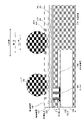
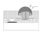
- FIG. 1 is a cross-sectional view showing a first example of a semiconductor package according to a first embodiment of the present technology.
- WLCSP Wafer Level Chip Size Package
- RDL Redistribution Layer
- This semiconductor package includes an IC (Integrated Circuit) 100 and an IC pad 190 for input/output.
- IC 100 is covered by an insulating layer 180 .
- the insulating layer 180 is made of, for example, a silicon nitride film (SiN).
- This semiconductor package comprises three insulating layers 210 , 220 and 230 .
- the RDL 300 which is a wiring layer, is formed between the first insulating layer 210 and the second insulating layer 220 .
- This RDL 300 includes a land 310 that connects to the underbump metal layer 400 as shown in FIG.
- FIG. 2 is a plan view showing a first example of the semiconductor package according to the first embodiment of the present technology; FIG.
- An under bump metal layer (UBM) 400 is a metal layer connected to the bumps 490 .
- An underbump metal layer 400 is formed between the second insulating layer 220 and the third insulating layer 230 .
- the under-bump metal layer 400 is connected to the bump 490 at the central portion and disposed on the second insulating layer 220 at the outer edge portion, resulting in an arched cross section.
- a bump 490 is a projecting electrode for input/output of this semiconductor package.
- This bump 490 is formed of, for example, a solder ball.
- an opening is provided in the outermost third insulating layer 230, and the surface other than the opening is covered with an SMD (Solder Mask Defined) structure. Therefore, the third insulating layer 230 is also called a solder resist.
- the diameter of the under bump metal layer 400 is formed so as to be larger than the opening diameter of the outermost layer.
- the under bump metal layer 400 inhibits or reduces transmission of force to the land 310 and the RDL 300 via the bumps 490, thereby improving drop test characteristics and impact resistance.
- the diameter of the under bump metal layer 400 is formed to be larger than the diameter of the land 310 in the RDL 300 connected to the under bump metal layer 400 .
- the wiring density between the bumps 490 can be improved. That is, even if the pitch between the underbump metal layers 400 is equal, if the diameter of the land 310 is small, part of the RDL 300 overlaps directly under the underbump metal layer 400, and a correspondingly large number of RDLs 300 are overlapped. be able to wire.
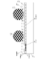
- FIG. 3 is a cross-sectional view showing a second example of the semiconductor package according to the first embodiment of the present technology.
- a second embodiment of this semiconductor package assumes a FOWLP (Fan Out Wafer Level Package).
- This FOWLP has a structure in which the terminals extend to the outside of the chip, as compared with the above-described WLCSP.
- This semiconductor package has a structure in which the IC 100 is sealed with a sealing resin 170 .
- the structure is the same as that of the first embodiment described above, except that the bumps 490 are located outside the IC 100 . That is, the diameter of the under-bump metal layer 400 is formed to be larger than the opening diameter of the outermost layer. As a result, the under bump metal layer 400 inhibits or reduces transmission of force to the land 310 and the RDL 300 via the bumps 490, thereby improving drop test characteristics and impact resistance.
- the diameter of the under bump metal layer 400 is formed to be larger than the diameter of the land 310 in the RDL 300 connected to the under bump metal layer 400 . Thereby, the wiring density between the bumps 490 can be improved.
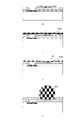
- FIG. 4 is a first diagram showing an example of the manufacturing process of the second example of the semiconductor package according to the first embodiment of the present technology.
- the IC 100 of a in the figure is attached to the support member 610 face down as shown in b of the figure.
- a sealing resin 170 As shown in c in the figure, it is resin-sealed with a sealing resin 170 .
- a material of the sealing resin 170 an epoxy resin, a phenol resin, or the like can be considered.
- the support material 610 is peeled off.
- a first insulating layer 210 is formed on the face-up surface by exposure and development technology.
- FIG. 5 is a second diagram showing a manufacturing process example of a second example of the semiconductor package according to the first embodiment of the present technology.
- the RDL 300 is formed on the first insulating layer 210 by a plating process. Then, as indicated by g in the figure, the second insulating layer 220 is formed by exposure and development techniques.
- an under bump metal layer 400 is formed.
- a material of the under-bump metal layer 400 for example, a Cu under-bump metal layer with a TiW seed layer and Ni as a barrier metal can be considered.
- a third insulating layer 230 is formed to form an SMD structure.
- a bump 490 that will be an external terminal is attached.
- FIG. 6 is a cross-sectional view showing a third example of the semiconductor package according to the first embodiment of the present technology.
- a third embodiment of this semiconductor package is a structure in which a copper pillar 390 is further provided in the FOWLP structure.
- the structure is the same as that of the above-described second embodiment. That is, the diameter of the under-bump metal layer 400 is formed to be larger than the opening diameter of the outermost layer.
- the under bump metal layer 400 inhibits or reduces transmission of force to the land 310 and the RDL 300 via the bumps 490, thereby improving drop test characteristics and impact resistance.
- the diameter of the under bump metal layer 400 is formed to be larger than the diameter of the land 310 in the RDL 300 connected to the under bump metal layer 400 . Thereby, the wiring density between the bumps 490 can be improved.
- FIG. 7 is a cross-sectional view showing a fourth example of the semiconductor package according to the first embodiment of the present technology.
- the fourth embodiment of this semiconductor package has a structure in which two layers of RDL 300 are provided in the WLCSP structure. Otherwise, the structure is the same as that of the first embodiment described above. That is, the diameter of the under-bump metal layer 400 is formed to be larger than the opening diameter of the outermost layer. As a result, the under bump metal layer 400 inhibits or reduces transmission of force to the land 310 and the RDL 300 via the bumps 490, thereby improving drop test characteristics and impact resistance.
- the diameter of the under bump metal layer 400 is formed to be larger than the diameter of the land 310 in the RDL 300 connected to the under bump metal layer 400 . Thereby, the wiring density between the bumps 490 can be improved.
- FIG. 8 is a cross-sectional view showing a fifth example of the semiconductor package according to the first embodiment of the present technology.
- the fifth embodiment of this semiconductor package has a structure in which two layers of RDL 300 are provided in the FOWLP structure. Other than that, the structure is the same as that of the above-described second embodiment. That is, the diameter of the under-bump metal layer 400 is formed to be larger than the opening diameter of the outermost layer. As a result, the under bump metal layer 400 inhibits or reduces transmission of force to the land 310 and the RDL 300 via the bumps 490, thereby improving drop test characteristics and impact resistance.
- the diameter of the under bump metal layer 400 is formed to be larger than the diameter of the land 310 in the RDL 300 connected to the under bump metal layer 400 . Thereby, the wiring density between the bumps 490 can be improved.
- the fifth embodiment assumes a structure in which two layers of RDL 300 are provided, three or more layers of RDL 300 may be provided.
- FIG. 9 is a cross-sectional view showing a sixth example of the semiconductor package according to the first embodiment of the present technology.
- the sixth embodiment of this semiconductor package has a structure in which two layers of RDL 300 are provided in the FOWLP structure, and a copper pillar 390 is further provided. Otherwise, the structure is the same as that of the fifth embodiment described above. That is, the diameter of the under-bump metal layer 400 is formed to be larger than the opening diameter of the outermost layer. As a result, the under bump metal layer 400 inhibits or reduces transmission of force to the land 310 and the RDL 300 via the bumps 490, thereby improving drop test characteristics and impact resistance.
- the diameter of the under bump metal layer 400 is formed to be larger than the diameter of the land 310 in the RDL 300 connected to the under bump metal layer 400 . Thereby, the wiring density between the bumps 490 can be improved.
- the sixth embodiment assumes a structure in which two layers of RDL 300 are provided, three or more layers of RDL 300 may be provided.
- the diameter of the under bump metal layer 400 is formed so as to be larger than the opening diameter of the outermost layer. This can inhibit or reduce the transmission of force to land 310 and RDL 300, thereby improving drop test characteristics and impact resistance.
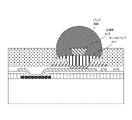
- FIG. 10 is a cross-sectional view showing a structural example of a semiconductor package according to a second embodiment of the present technology
- the underbump metal layer 400 has a protrusion 410 at the interface with the bump 490 .
- the protrusion 410 is formed by the same metal (eg, copper) plating as the RDL 300, with nickel (Ni) or nickel gold (Ni/Au) plating added as necessary.
- the diameter of the under bump metal layer 400 is formed to be larger than the diameter of the opening in the outermost layer, as in the first embodiment described above. Also, the diameter of the under bump metal layer 400 is formed to be larger than the diameter of the land 310 in the RDL 300 connected to the under bump metal layer 400 .
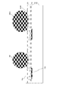
- FIG. 11 is a plan view showing an arrangement example of protrusions 410 according to the second embodiment of the present technology.
- protrusions 410 having a cross-shaped or L-shaped planar shape with a large convex area for the corner terminals arranged on the outer periphery of the chip. As a result, it is possible to further strengthen the connection of the bumps in the outer peripheral portion of the chip.
- FIG. 12 is a plan view showing a planar shape example of the protrusion 410 according to the second embodiment of the present technology.
- a in the figure is an example of the shape of the oval protrusion 410.
- FIG. b in the figure is an example of the shape of the L-shaped protrusion 410 .
- c in the figure is an example of the shape of the cross-shaped projection 410 .
- D in the figure is an example of the shape of the protrusion 410 obtained by dividing an oval into a plurality of parts.
- e in the figure is an example of the shape of the projection 410 obtained by dividing the L-shaped shape into a plurality of pieces.
- f in the figure is an example of the shape of the projection 410 obtained by dividing the cross shape into a plurality of pieces.
- FIG. 13 is a first diagram showing an example of the manufacturing process of the protrusion 410 according to the second embodiment of the present technology.
- a resist 620 for forming the projections 410 is applied as shown in b in the figure. Then, as indicated by c in the figure, the unnecessary portion 621 is removed by exposure and development.
- a protrusion 410 is formed by copper plating. Moreover, if necessary, nickel (Ni) or nickel gold (Ni/Au) plating may be added.
- FIG. 14 is a second diagram showing an example of the manufacturing process of the protrusion 410 according to the second embodiment of the present technology.
- the resist 620 for forming the protrusions 410 is removed, as indicated by e in the figure. Then, a resist 630 for forming the third insulating layer 230 is applied, as indicated by f in FIG. Thereafter, as indicated by g in the figure, the unnecessary portion 631 is removed by exposure and development.
- bumps 490 are formed by reflow.
- the under bump metal layer 400 has the protrusion 410 at the interface with the bump 490, thereby making the connection between the under bump metal layer 400 and the bump 490. can be strengthened.
- FIG. 15 is a cross-sectional view showing a modification of the protrusion shape according to the second embodiment of the present technology.
- a modification of the protrusion shape in the second embodiment is a structure in which a reverse tapered metal column 412 is formed on a mushroom-shaped bump 411 and covered with a solder ball to generate a bump 490 . Forming the reverse tapered metal column 412 in the bump 490 in this way has the effect of strengthening the connection with the bump 490 .
- FIG. 16 is a cross-sectional view showing a structural example of a semiconductor package according to a third embodiment of the present technology.
- the semiconductor package according to the third embodiment has a structure in which base portions of bumps 490 are covered with resin 499 for reinforcement. This figure shows a state in which the chip is mounted face down on the mounting board 500 . By reinforcing with the resin 499, the connection of the bumps 490 can be strengthened.
- the diameter of the under-bump metal layer 400 is formed to be larger than the opening diameter of the outermost layer, as in the first embodiment described above. Also, the diameter of the under bump metal layer 400 is formed to be larger than the diameter of the land 310 in the RDL 300 connected to the under bump metal layer 400 .
- FIG. 17 is a plan view showing an arrangement example of the resin 499 according to the third embodiment of the present technology.
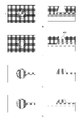
- the regions to be reinforced with the resin 499 are provided at the four corners of the semiconductor package where strain concentrates. Also, as shown in FIG. 4c, the entire semiconductor package may be covered with resin 499 if necessary. However, the larger the area covered by the resin 499, the more likely the package is to warp due to the difference in linear expansion coefficient between the silicon of the semiconductor package and the resin 499. Therefore, which type should be selected according to the package size. It is necessary to select appropriately.
- FIG. 18 is a first diagram showing a first example of the process of forming the resin 499 according to the third embodiment of the present technology.
- resin sealing is performed by screen printing.
- a wafer on which bumps 490 are already mounted is prepared, as indicated by a in FIG.
- a resin printing screen 660 is set on the side on which the bumps 490 are mounted.
- This resin printing screen 660 comprises a bump mask 661 for masking the bumps 490 and a dicing area mask 662 for masking the dicing area.
- liquid resin 498 is screen-printed by a squeegee 663, as shown in c in the figure.
- FIG. 19 is a second diagram showing a first example of a process of forming the resin 499 according to the third embodiment of the present technology.
- the resin printing screen 660 is removed.
- the liquid resin 498 is heated and cured as indicated by e in FIG.
- the liquid resin 498 hardens and shrinks and becomes lower than the height of the bumps 490 .
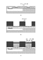
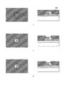
- FIG. 20 is a first diagram showing a second example of the process of forming the resin 499 according to the third embodiment of the present technology.
- resin sealing is performed using a molding die.
- a wafer 101 on which bumps 490 are already mounted is prepared, as indicated by a in FIG. Then, the wafer 101 is set in molds 671 and 672 as shown in b in FIG. An elastic release film 679 is attached to the mold 671 on the upper side.
- liquid resin 498 or granular resin is supplied to the side of the wafer 101 on which the bumps 490 are mounted. Then, as indicated by d in the figure, pressurization and heat curing are performed.
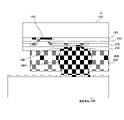
- the release film 679 is peeled off and the wafer 101 is taken out. Then, as indicated by f in the figure, dicing is performed to cut into individual pieces.
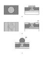
- FIG. 21 is a second diagram showing a second example of the process of forming the resin 499 according to the third embodiment of the present technology.
- the figure shows how the liquid resin 498 is supplied, pressurized and heat-cured.
- the bump 490 is positioned by applying pressure from above through the release film 679 . As a result, a part of the bump 490 is exposed from the resin 499 after the release film 679 is peeled off.
- the connection of the bump 490 is strengthened and strain concentrated on the bump root portion of the package corner is reduced. can do.
- repair becomes easy, and a component mounting prohibition area around the package can be eliminated.
- FIG. 22 is a cross-sectional view showing a first example of the structure of the semiconductor package according to the fourth embodiment of the present technology
- At least part of the bumps 490 have an oval planar shape. Thereby, the stress acting on the bump 490 can be reduced.
- the bump 490 has an oval shape with a short axis d(x) and a long axis d(y).
- the shape of the opening of the third insulating layer 230 and the shape of the bump 490 are the same oval shape.
- the diameter of the under bump metal layer 400 is made larger than any of the opening diameters of the outermost layer, as in the first embodiment. It is formed. Also, the diameter of the under bump metal layer 400 is formed to be larger than the diameter of any of the lands 310 in the RDL 300 connected to the under bump metal layer 400 .
- the bumps 490 can be adjusted so that they are rotated to the right by a predetermined angle (n°) from their respective central axes.
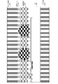
- FIG. 23 is a plan view showing a first arrangement example of bumps 490 according to the fourth embodiment of the present technology.
- each of the bumps 490 is all oval shaped, and all are laid out radially from the center of the chip or package.
- FIG. 24 is a plan view showing a second arrangement example of bumps 490 according to the fourth embodiment of the present technology.
- each of the bumps 490 has a layout that spreads radially from the center of the chip or package in the region where the diagonal lines of the chip or package straddle.
- the bumps 490 in other regions may have an oval shape rotated vertically or horizontally as indicated by a in the figure, or may be circular as indicated by b in the same figure.
- an IC chip exists in the central area, and the stress acting on the IC chip can be reduced by arranging a layout in which the bumps 490 in the central area spread radially. can be done.
- FIG. 25 is a plan view showing a third arrangement example of bumps 490 according to the fourth embodiment of the present technology.
- FIG. 26 is a plan view showing a fourth arrangement example of bumps 490 according to the fourth embodiment of the present technology.
- the bumps 490 are arranged only on the outer peripheral portion of the chip or package as indicated by a in the figure, or only on the outer peripheral portion and the central portion as indicated by b in the same figure.
- Each of the bumps 490 are all oval shaped and all radiate out from the center of the chip or package.
- FIG. 27 is a plan view showing a fifth arrangement example of bumps 490 according to the fourth embodiment of the present technology.
- the bumps 490 are laid out radially from the center of the chip or package at the four corners.
- the bumps 490 are not arranged in any part other than the outer peripheral part.
- the bumps 490 on the outer periphery other than the four corners may have an oval shape rotated vertically or horizontally as indicated by a in FIG. There may be.
- FIG. 28 is a plan view showing a sixth arrangement example of bumps 490 according to the fourth embodiment of the present technology.
- only the four corner bumps 490 have an oval shape that spreads radially from the center of the chip or package.
- Circular bumps may be arranged in the outer peripheral portion as indicated by a in the same figure, and circular bumps may be further arranged in the central portion as indicated by b in the same figure.
- FIG. 29 is a first diagram showing an example of the formation process of the bumps 490 of the first example in the fourth embodiment of the present technology.
- a metal mask 641 having oval openings is used, and a squeegee 642 is used to fill the paste-like solder 495, followed by solder printing. After solder printing, the metal mask 641 is removed.
- FIG. 30 is a second diagram showing an example of the formation process of the bumps 490 of the first example in the fourth embodiment of the present technology.
- a shows how a metal mask 641 having an oval opening is used to fill paste-like solder 495 with a squeegee 642 .
- b in the same figure shows a state in which an oval bump 490 is formed after reflow.
- FIG. 31 is a cross-sectional view showing a second example of the structure of the semiconductor package according to the fourth embodiment of the present technology.
- a copper pillar bump 493 is formed on the underbump metal layer 400, and solder 491 is formed thereon with nickel 492 interposed therebetween. Similar to the first embodiment described above, the copper pillar bump 493 is oval shaped with a minor axis d(x) and a major axis d(y).
- the shape of the opening of the third insulating layer 230 may be the same oval shape as the copper pillar bump 493 , or may be a circular shape different from that of the copper pillar bump 493 .
- the diameter of the under bump metal layer 400 is formed to be larger than the opening diameter of the outermost layer, as in the first embodiment. be. Also, the diameter of the under bump metal layer 400 is formed to be larger than the diameter of the land 310 in the RDL 300 connected to the under bump metal layer 400 . Also, as in the first embodiment described above, the copper pillar bumps 493 can be adjusted to be rotated to the right by a predetermined angle (n°) from their central axes.
- FIG. 32 is a first diagram showing an example of a process for forming the copper pillar bumps 493 of the second example according to the fourth embodiment of the present technology.
- the third insulating layer 230 is formed, as indicated by a in the figure.
- the shape of the opening of the third insulating layer 230 may be oval or circular.
- the direction of the opening is the same as that of the copper pillar bumps 493 to be formed later.
- a barrier seed metal layer 643 is formed by a PVD (Plasma Vapor Deposition) process.
- a photoresist 644 is applied as shown in b in the figure. Then, a pattern is formed in the photoresist 644 by a lithography process.
- the shape of the opening in photoresist 644 is an oval shape with a short axis and a long axis. The orientation of the opening can be arbitrarily adjusted.
- copper 497 is plated by an electrolytic plating process.
- Nickel 496 and solder 495 are then plated by an electroless plating process.
- FIG. 33 is a second diagram showing an example of a process for forming the copper pillar bumps 493 of the second example according to the fourth embodiment of the present technology.
- the barrier seed metal layer 643 is removed by an etching process. After that, as shown by e in the figure, by performing reflow, an oval-shaped copper pillar bump 493 is formed.
- the stress of the chip can be alleviated by forming the bumps in an oval shape and extending the directions radially. Also, by adjusting the layout of the oval bumps, it is possible to prevent warping of the chip due to thermal contraction.
- FIG. 34 is a cross-sectional view showing a first example of the structure of the semiconductor package according to the fifth embodiment of the present technology
- FIG. 35 is a plan view showing a first example of the structure of the semiconductor package according to the fifth embodiment of the present technology
- the size of the bumps 490A at the four corners to which greater stress is applied is increased to increase the height.
- the stress of the corner portion can be absorbed and the stress resistance can be improved.
- the bump 490A with a larger size has a structure in which the number of layers of the RDL 300 is reduced.
- the under bump metal layer 400 of the corner bump 490A is formed between the second insulating layer 220 and the third insulating layer 230, and the under bump metal layer 400 of the other bumps 490 is formed between the third insulating layer 230 and the bump 490A. It is formed between the fourth insulating layer 240 and the fourth insulating layer 240 .
- the diameter of the under-bump metal layer 400 is formed to be larger than the opening diameter of the outermost layer, similarly to the above-described first embodiment. be. Also, the diameter of the under bump metal layer 400 is formed to be larger than the diameter of the land in the RDL 300 connected to the under bump metal layer 400 .
- increasing the bump size is not limited to only the corners, and the bumps in the vicinity of the corners may be increased.
- FIG. 36 is another plan view showing the first example of the structure of the semiconductor package according to the fifth embodiment of the present technology.
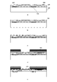
- FIG. 37 is a first diagram showing an example of the bump formation process of the first example in the fifth embodiment of the present technology.
- the process up to the middle is the same as the manufacturing process of the FOWLP of the two-layer RDL in the fifth example of the first embodiment described above, but as shown in a in the figure, when forming the second layer of the RDL, Then, the under bump metal layer 400 is formed only at the positions corresponding to the corner bumps. After that, a resist 645 is applied as indicated by b in FIG. The part forming 400 is opened.
- a mask 646 is formed as indicated by d in FIG. 11 to mask the portion for forming the under bump metal layer 400 corresponding to the corner bump, and a normal bump is formed as indicated by e in FIG. An under-bump metal layer 400 corresponding to is formed.
- FIG. 38 is a second diagram showing an example of the bump formation process of the first example in the fifth embodiment of the present technology.
- the mask is removed as indicated by f in the figure, and a resist 647 is applied as indicated by g in the figure.
- the under bump metal layer 400 is opened.
- bumps 490 and 490A are formed by reflow.
- the solder balls are mounted, bumps 490A of the corner portions are of a large size.
- the size of the balls is adjusted so that the heights of the bumps after reflow are uniform.
- FIG. 39 is a cross-sectional view showing a second example of the structure of the semiconductor package according to the fifth embodiment of the present technology
- FIG. 40 is a plan view showing a second example of the structure of the semiconductor package according to the fifth embodiment of the present technology
- the second example of the fifth embodiment has a structure in which the diameters of the bumps 490B and the underbump metal layer 400B at the four corners where greater stress is applied are increased. Thereby, the stress of the corner portion can be absorbed and the stress resistance can be improved. In this way, by increasing the diameter of the under-bump metal layer 400B of the corner bump where a larger stress is applied to the mounting reliability and the risk of breakage is increased first, and also by increasing the diameter of the bump 490B, the corner bump is reduced. can enhance the stress resistance of However, it is necessary to adjust the diameters of the under bump metal layer 400B and the bumps 490B to appropriate sizes in order to match the height of each bump that is finally formed.
- the diameters of the under bump metal layers 400 and 400B are set to be larger than the opening diameter of the outermost layer, as in the first embodiment. It is formed. Also, the diameters of the under bump metal layers 400 and 400B are formed to be larger than the diameter of the land in the RDL 300 connected to the under bump metal layers 400 or 400B.
- increasing the diameters of the under bump metal layer 400B and the bumps 490B is not limited to the corners, and may be performed near the corners.
- FIG. 41 is another plan view showing the second example of the structure of the semiconductor package according to the fifth embodiment of the present technology.
- the stress resistance is enhanced by increasing the height or diameter of the bumps where stress is more concentrated and breakage may occur first. , it is possible to improve the durability of mounting reliability as a package.
- FIG. 42 is a cross-sectional view showing a first example of the structure of the semiconductor package according to the sixth embodiment of the present technology
- the under-bump metal layer 400 has a protrusion 420 at the interface with the second insulating layer 220 facing the bottom of the under-bump metal layer among the plurality of insulating layers. Accordingly, by providing the concave portion in the second insulating layer 220, impact resistance can be improved.
- the diameter of the under bump metal layer 400 is formed to be larger than the opening diameter of the outermost layer, as in the first embodiment. be. Also, the diameter of the under bump metal layer 400 is formed to be larger than the diameter of the land 310 in the RDL 300 connected to the under bump metal layer 400 .
- FIG. 43 is a cross-sectional view showing a second example of the structure of the semiconductor package according to the sixth embodiment of the present technology.
- the under bump metal layer 400 has protrusions 430 at the interface with the third insulating layer 230, which is the outermost layer among the plurality of insulating layers.
- mounting reliability can be improved by improving adhesion with the third insulating layer 230 .
- the diameter of the under bump metal layer 400 is formed to be larger than the opening diameter of the outermost layer, as in the first embodiment. be. Also, the diameter of the under bump metal layer 400 is formed to be larger than the diameter of the land 310 in the RDL 300 connected to the under bump metal layer 400 .
- FIG. 44 is a cross-sectional view showing a first structural example of a semiconductor package according to a seventh embodiment of the present technology.
- a cushion pad 494 having an overhang shape is provided between the bump 490 and the under bump metal layer 400 .
- This cushion pad 494 is formed containing copper as a material, for example.
- the cushion pad 494 diffuses the thermal stress to the third insulating layer 230 on the surface, thereby diffusing the stress.
- FIG. 45 is a cross-sectional view showing a second structural example of the semiconductor package according to the seventh embodiment of the present technology.
- the surface of the cushion pad 494 is provided with projections or recesses. Thereby, the adhesion between the cushion pad 494 and the bump 490 can be improved, and the mounting reliability can be improved.
- FIG. 46 is a cross-sectional view showing a modified example of the cushion pad 494 according to the seventh embodiment of the present technology.
- a in the figure has a structure in which the mushroom-shaped canopy portion of the cushion pad 494 is flattened. Even in this case, the stress can be diffused because the cushion pad 494 itself has an overhang shape.
- the diameter of the under bump metal layer 400 is formed to be larger than the opening diameter of the outermost layer, as in the first embodiment. Also, the diameter of the under bump metal layer 400 is formed to be larger than the diameter of the land 310 in the RDL 300 connected to the under bump metal layer 400 .
- thermal stress can be reduced by the third insulation of the surface layer. It can diffuse into layer 230 to spread the stress.
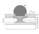
- FIG. 47 is a cross-sectional view showing a first structural example of a semiconductor package according to an eighth embodiment of the present technology.
- an underbump metal layer is formed from land 401 and seed layer 402 .
- the seed layer 402 is a seed layer for via filling plating, and is a sputtered film lamination of titanium copper alloy (Ti/Cu) or the like.
- the land 401 has a structure in which, for example, copper is embedded on the seed layer 402 .
- the seed layer 402 has a tapered shape, and the side surface 408 of the cross section has a gentle slope of the radius of curvature.
- the radius of curvature of the side surface 408 is desirably 10 ⁇ m or more, for example.
- a metal post 403 is provided between the RDL 300 and the seed layer 402 .
- the metal pillars 403 are formed by copper plating, for example.
- the metal column 403 has a tapered shape, and the side surface 409 of the cross section has a gentle slope of curvature radius.
- the radius of curvature of the side surface 409 is desirably 10 ⁇ m or more, for example.
- the height x of the side surface of the seed layer 402 and the height y of the side surface of the metal column 403 are equal. Therefore, the structure is suitable for the case where the stress concentration needs to be evenly distributed vertically.
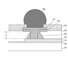
- FIG. 48 is a cross-sectional view showing a second structural example of the semiconductor package according to the eighth embodiment of the present technology.
- the height x of the side surface of the seed layer 402 is higher than the height y of the side surface of the metal column 403 . Therefore, the structure is suitable when the stress at the bottom needs to be smaller than the stress at the top.
- FIG. 49 is a cross-sectional view showing a third structural example of the semiconductor package according to the eighth embodiment of the present technology.
- the height x of the side surface of the seed layer 402 is lower than the height y of the side surface of the metal column 403 . Therefore, the structure is suitable when the stress on the top needs to be smaller than the stress on the bottom.
- the diameters of the land 401 and the seed layer 402 are formed to be larger than the opening diameter of the outermost layer. Also, the diameters of the land 401 and the seed layer 402 are formed to be larger than the diameter of the land 310 in the RDL 300 connected to the metal column 403 .
- FIG. 50 is a first diagram showing an example of a manufacturing process for a semiconductor package according to the eighth embodiment of the present technology.
- a seed layer 402 is formed on the first insulating layer 210 by sputtering a titanium-copper alloy (Ti/Cu) or the like. Then, a plating resist 651 is applied, exposed and developed for patterning.
- Ti/Cu titanium-copper alloy
- a plating resist 652 is applied.
- FIG. 51 is a second diagram showing an example of the manufacturing process of the semiconductor package according to the eighth embodiment of the present technology.
- the plating resist 652 is exposed and developed. Underexposure is performed during exposure. As a result, the plating resist 652 is formed into a reverse tapered shape.
- FIG. 52 is a third diagram showing an example of the manufacturing process of the semiconductor package according to the eighth embodiment of the present technology.
- a material for the insulating layer 653 is applied.
- Polyimide (PI) or polybenzoxazole (PBO) can be used as the material of the insulating layer 653 .
- the oxide film on the copper is removed.
- the corners of the opening are chamfered by pre-cleaning (sputter etching) before seed sputtering.
- pre-cleaning sputter etching
- the surface of the copper pillar exposed from the opening and having oxide films and residues of the insulating layer resin remaining is cleaned.
- the steep corners of the opening corners are also etched by this sputter etching.
- FIG. 53 is a fourth diagram showing an example of the manufacturing process of the semiconductor package according to the eighth embodiment of the present technology.
- seed sputtering for forming the seed layer 402 is performed as indicated by l in the figure.
- a sputtered film stack of titanium copper alloy (Ti/Cu) is formed.
- an opening is formed in the plating resist 654 as indicated by m in the figure. That is, a plating resist 654 is applied, and exposure and development are performed. Then, as indicated by n in the figure, a land 401 is formed above the via by copper plating. After that, the plating resist 654 is removed as indicated by o in FIG.
- FIG. 54 is a fifth diagram showing an example of the manufacturing process of the semiconductor package according to the eighth embodiment of the present technology.
- seed etching is performed to remove unnecessary portions of the seed layer 402, as indicated by p in FIG.
- a solder resist for the third insulating layer 230 is applied, exposed, developed, and cured.
- the bumps 490 are mounted by reflow. At that time, the unnecessary oxide film is removed and the flux is applied.
- the metal column 403 having a cross section with a gentle curvature radius is formed at the bottom of the via, and the insulating layer opening is formed at the top of the via with a gentle curvature radius by a seed layer forming process or the like.
- a seed layer 402 is formed, and then a land 401 is formed by copper embedding plating.
- FIG. 55 is a perspective view showing an external configuration example of an electronic device 700 including a semiconductor package according to an embodiment of the present technology.
- This electronic device 700 has an appearance in which components are arranged inside and outside an outer casing 701 formed in a horizontally long flat shape, for example.
- Electronic device 700 may be, for example, a device used as a game device.
- a display panel 702 is provided on the front surface of the outer casing 701 in the central portion in the longitudinal direction.
- operation keys 703 and 704 are arranged separately in the circumferential direction.
- An operation key 705 is provided at the lower end of the front surface of the outer casing 701 .
- Operation keys 703, 704, and 705 function as direction keys, enter keys, or the like, and are used to select menu items displayed on the display panel 702, progress the game, and the like.
- connection terminals 706 for connecting external devices, supply terminals 707 for power supply, light receiving windows 708 for infrared communication with external devices, and the like are provided.
- FIG. 56 is a block diagram showing a functional configuration example of an electronic device 700 including a semiconductor package according to the embodiment of the present technology.
- the electronic device 700 includes a main CPU (Central Processing Unit) 710 and a system controller 720 . Power is supplied to the main CPU 710 and the system controller 720 from, for example, a battery (not shown) through different systems.
- the main CPU 710 includes a menu processing unit 711 that generates a menu screen for allowing the user to set various types of information or select an application, and an application processing unit 712 that executes applications.
- the electronic device 700 also includes a setting information holding unit 730 such as a memory that holds various information set by the user. Information set by the user is sent to the setting information holding unit 730 from the main CPU 710, and the setting information holding unit 730 holds the sent information.
- a setting information holding unit 730 such as a memory that holds various information set by the user. Information set by the user is sent to the setting information holding unit 730 from the main CPU 710, and the setting information holding unit 730 holds the sent information.
- the system controller 720 includes an operation input receiving section 721 , a communication processing section 722 and a power control section 723 .
- the operation input reception unit 721 detects the states of the operation keys 703 , 704 and 705 .
- the communication processing unit 722 performs communication processing with an external device.
- the power control unit 723 controls power supplied to each unit of the electronic device 700 .
- the semiconductor package according to the embodiment of the present technology is mounted on at least one of the main CPU 710 , the system controller 720 and the setting information holding unit 730 .
- the electronic device 700 can improve drop test characteristics and impact resistance.
- the present technology can also have the following configuration.
- the bump further includes a metal column bump at a connection portion with the under bump metal layer.
- the bumps are higher at four corners of a predetermined region than other bumps.
- the bumps are higher than other bumps in the peripheral portion of the predetermined area.
- the bump has a larger diameter at four corners of a predetermined area than other bumps.
Landscapes
- Wire Bonding (AREA)
- Physics & Mathematics (AREA)
- Geometry (AREA)
- Internal Circuitry In Semiconductor Integrated Circuit Devices (AREA)
- Engineering & Computer Science (AREA)
- Manufacturing & Machinery (AREA)
Abstract
Description
1.第1の実施の形態(UBM径と開口径の関係)
2.第2の実施の形態(パッケージ付け根の保護)
3.第3の実施の形態(UBMからバンプへの突起)
4.第4の実施の形態(小判型バンプ)
5.第5の実施の形態(バンプサイズ)
6.第6の実施の形態(UBMから絶縁層への突起)
7.第7の実施の形態(クッションパッド)
8.第8の実施の形態(UBMが所定の曲率半径によるテーパ形状)
9.適用例
[第1の実施例]
図1は、本技術の第1の実施の形態における半導体パッケージの第1の実施例を示す断面図である。
図3は、本技術の第1の実施の形態における半導体パッケージの第2の実施例を示す断面図である。
図6は、本技術の第1の実施の形態における半導体パッケージの第3の実施例を示す断面図である。
図7は、本技術の第1の実施の形態における半導体パッケージの第4の実施例を示す断面図である。
図8は、本技術の第1の実施の形態における半導体パッケージの第5の実施例を示す断面図である。
図9は、本技術の第1の実施の形態における半導体パッケージの第6の実施例を示す断面図である。
図10は、本技術の第2の実施の形態における半導体パッケージの構造例を示す断面図である。
図15は、本技術の第2の実施の形態における突起形状の変形例を示す断面図である。
図16は、本技術の第3の実施の形態における半導体パッケージの構造例を示す断面図である。
[第1の実施例]
図22は、本技術の第4の実施の形態における半導体パッケージの構造の第1の実施例を示す断面図である。
図31は、本技術の第4の実施の形態における半導体パッケージの構造の第2の実施例を示す断面図である。
[第1の実施例]
図34は、本技術の第5の実施の形態における半導体パッケージの構造の第1の実施例を示す断面図である。図35は、本技術の第5の実施の形態における半導体パッケージの構造の第1の実施例を示す平面図である。
図39は、本技術の第5の実施の形態における半導体パッケージの構造の第2の実施例を示す断面図である。図40は、本技術の第5の実施の形態における半導体パッケージの構造の第2の実施例を示す平面図である。
[第1の実施例]
図42は、本技術の第6の実施の形態における半導体パッケージの構造の第1の実施例を示す断面図である。
図43は、本技術の第6の実施の形態における半導体パッケージの構造の第2の実施例を示す断面図である。
図44は、本技術の第7の実施の形態における半導体パッケージの第1の構造例を示す断面図である。
図47は、本技術の第8の実施の形態における半導体パッケージの第1の構造例を示す断面図である。
図55は、本技術の実施の形態における半導体パッケージを備える電子機器700の外観構成例を示す斜視図である。
(1)複数の絶縁層と、
前記複数の絶縁層のうち最表層の開口部において一部が露出してバンプに接続するアンダーバンプ金属層とを具備し、
前記アンダーバンプ金属層の径は、前記開口部の径より大きい
半導体パッケージ。
(2)前記アンダーバンプ金属層に接続する少なくとも1層の再配線層をさらに具備する前記(1)に記載の半導体パッケージ。
(3)前記アンダーバンプ金属層の径は、前記アンダーバンプ金属層に接続する前記再配線層におけるランドの径より大きい
前記(2)に記載の半導体パッケージ。
(4)前記アンダーバンプ金属層の直下に前記再配線層の一部がオーバラップして配置される
前記(2)に記載の半導体パッケージ。
(5)前記アンダーバンプ金属層は、前記バンプとの界面に突起を備える
前記(1)から(4)のいずれかに記載の半導体パッケージ。
(6)前記突起は、所定の平面形状を備える
前記(5)に記載の半導体パッケージ。
(7)前記突起は、前記バンプに相対して逆テーパの柱形状を備える
前記(5)に記載の半導体パッケージ。
(8)二次元状に複数配置される前記アンダーバンプ金属層と前記バンプとの接続部分のうち少なくとも一部を覆う樹脂をさらに具備する前記(1)から(7)のいずれかに記載の半導体パッケージ。
(9)前記樹脂は、所定の領域の四隅に形成される
前記(8)に記載の半導体パッケージ。
(10)前記樹脂は、所定の領域の外周部分に形成される
前記(8)に記載の半導体パッケージ。
(11)前記バンプは、二次元状に複数配置される前記アンダーバンプ金属層と前記バンプとの接続部分のうち少なくとも一部において小判型の平面形状を備える
前記(1)から(10)のいずれかに記載の半導体パッケージ。
(12)前記小判型の平面形状を備えるバンプは、所定の領域の四隅に形成される
前記(11)に記載の半導体パッケージ。
(13)前記小判型の平面形状を備えるバンプは、所定の領域の外周部分に形成される
前記(11)に記載の半導体パッケージ。
(14)前記小判型の平面形状を備えるバンプは、所定の領域において放射状に広がる傾きを備える
前記(11)に記載の半導体パッケージ。
(15)前記バンプは、前記アンダーバンプ金属層との接続部分において金属柱バンプをさらに備える
前記(11)に記載の半導体パッケージ。
(16)前記バンプは、所定の領域の四隅においてそれ以外のバンプよりも高さが高い
前記(1)から(15)のいずれかに記載の半導体パッケージ。
(17)前記バンプは、所定の領域の外周部分においてそれ以外のバンプよりも高さが高い
前記(1)から(15)のいずれかに記載の半導体パッケージ。
(18)前記バンプは、所定の領域の四隅においてそれ以外のバンプよりも径が大きい
前記(1)から(15)のいずれかに記載の半導体パッケージ。
(19)前記バンプは、所定の領域の外周部分においてそれ以外のバンプよりも径が大きい
前記(1)から(15)のいずれかに記載の半導体パッケージ。
(20)前記アンダーバンプ金属層は、前記複数の絶縁層のうち前記アンダーバンプ金属層の下部に面した絶縁層との界面に突起を備える
前記(1)から(19)のいずれかに記載の半導体パッケージ。
(21)前記アンダーバンプ金属層は、前記複数の絶縁層のうち前記最表層との界面に突起を備える
前記(1)から(20)のいずれかに記載の半導体パッケージ。
(22)前記バンプと前記アンダーバンプ金属層との間に張り出し形状を有するクッションパッドをさらに具備する前記(1)から(21)のいずれかに記載の半導体パッケージ。
(23)前記クッションパッドは、表面に凹凸部を備える
前記(22)に記載の半導体パッケージ。
(24)前記アンダーバンプ金属層は、第1の曲率半径を有するテーパ形状を備える
前記(1)から(23)のいずれかに記載の半導体パッケージ。
(25)前記アンダーバンプ金属層と前記再配線層との間を接続して第2の曲率半径を有するテーパ形状を備える金属柱をさらに具備する
前記(24)に記載の半導体パッケージ。
(26)複数の絶縁層と、前記複数の絶縁層のうち最表層の開口部において一部が露出してバンプに接続するアンダーバンプ金属層とを備えて、前記アンダーバンプ金属層の径が前記開口部の径より大きい半導体パッケージを具備する電子機器。
101 ウエハー
170 封止樹脂
180 絶縁層
190 ICパッド
210、220、230、240 絶縁層
300 RDL(Redistribution Layer:再配線層)
310 ランド
390 銅ピラー
400、400B アンダーバンプ金属層(UBM:Under Bump Metal)
401 ランド
402 シード層
403 金属柱
410、420、430 突起
411 キノコ状バンプ
412 金属柱
490、490A、490B バンプ
491 半田
492 ニッケル
493 銅ピラーバンプ
494 クッションパッド
495 半田
496 ニッケル
497 銅
498 液状樹脂
499 樹脂
500 実装基板
610 サポート材
620、630 レジスト
641 メタルマスク
642 スキージ
643 バリアシードメタル層
644 フォトレジスト
645 レジスト
646 マスク
647 レジスト
651、652、654 メッキレジスト
653 絶縁層
660 樹脂印刷スクリーン
661 バンプマスク
662 ダイシングエリアマスク
663 スキージ
671、672 モールド金型
679 離型フィルム
700 電子機器
Claims (26)
- 複数の絶縁層と、
前記複数の絶縁層のうち最表層の開口部において一部が露出してバンプに接続するアンダーバンプ金属層とを具備し、
前記アンダーバンプ金属層の径は、前記開口部の径より大きい
半導体パッケージ。 - 前記アンダーバンプ金属層に接続する少なくとも1層の再配線層をさらに具備する請求項1記載の半導体パッケージ。
- 前記アンダーバンプ金属層の径は、前記アンダーバンプ金属層に接続する前記再配線層におけるランドの径より大きい
請求項2記載の半導体パッケージ。 - 前記アンダーバンプ金属層の直下に前記再配線層の一部がオーバラップして配置される
請求項2記載の半導体パッケージ。 - 前記アンダーバンプ金属層は、前記バンプとの界面に突起を備える
請求項1記載の半導体パッケージ。 - 前記突起は、所定の平面形状を備える
請求項5記載の半導体パッケージ。 - 前記突起は、前記バンプに相対して逆テーパの柱形状を備える
請求項5記載の半導体パッケージ。 - 二次元状に複数配置される前記アンダーバンプ金属層と前記バンプとの接続部分のうち少なくとも一部を覆う樹脂をさらに具備する請求項1記載の半導体パッケージ。
- 前記樹脂は、所定の領域の四隅に形成される
請求項8記載の半導体パッケージ。 - 前記樹脂は、所定の領域の外周部分に形成される
請求項8記載の半導体パッケージ。 - 前記バンプは、二次元状に複数配置される前記アンダーバンプ金属層と前記バンプとの接続部分のうち少なくとも一部において小判型の平面形状を備える
請求項1記載の半導体パッケージ。 - 前記小判型の平面形状を備えるバンプは、所定の領域の四隅に形成される
請求項11記載の半導体パッケージ。 - 前記小判型の平面形状を備えるバンプは、所定の領域の外周部分に形成される
請求項11記載の半導体パッケージ。 - 前記小判型の平面形状を備えるバンプは、所定の領域において放射状に広がる傾きを備える
請求項11記載の半導体パッケージ。 - 前記バンプは、前記アンダーバンプ金属層との接続部分において金属柱バンプをさらに備える
請求項11記載の半導体パッケージ。 - 前記バンプは、所定の領域の四隅においてそれ以外のバンプよりも高さが高い
請求項1記載の半導体パッケージ。 - 前記バンプは、所定の領域の外周部分においてそれ以外のバンプよりも高さが高い
請求項1記載の半導体パッケージ。 - 前記バンプは、所定の領域の四隅においてそれ以外のバンプよりも径が大きい
請求項1記載の半導体パッケージ。 - 前記バンプは、所定の領域の外周部分においてそれ以外のバンプよりも径が大きい
請求項1記載の半導体パッケージ。 - 前記アンダーバンプ金属層は、前記複数の絶縁層のうち前記アンダーバンプ金属層の下部に面した絶縁層との界面に突起を備える
請求項1記載の半導体パッケージ。 - 前記アンダーバンプ金属層は、前記複数の絶縁層のうち前記最表層との界面に突起を備える
請求項1記載の半導体パッケージ。 - 前記バンプと前記アンダーバンプ金属層との間に張り出し形状を有するクッションパッドをさらに具備する請求項1記載の半導体パッケージ。
- 前記クッションパッドは、表面に凹凸部を備える
請求項22記載の半導体パッケージ。 - 前記アンダーバンプ金属層は、第1の曲率半径を有するテーパ形状を備える
請求項1記載の半導体パッケージ。 - 前記アンダーバンプ金属層と前記再配線層との間を接続して第2の曲率半径を有するテーパ形状を備える金属柱をさらに具備する
請求項24記載の半導体パッケージ。 - 複数の絶縁層と、前記複数の絶縁層のうち最表層の開口部において一部が露出してバンプに接続するアンダーバンプ金属層とを備えて、前記アンダーバンプ金属層の径が前記開口部の径より大きい半導体パッケージを具備する電子機器。
Priority Applications (4)
| Application Number | Priority Date | Filing Date | Title |
|---|---|---|---|
| CN202180098373.5A CN117397017A (zh) | 2021-05-25 | 2021-12-28 | 半导体封装和电子装置 |
| JP2023523958A JPWO2022249526A1 (ja) | 2021-05-25 | 2021-12-28 | |
| KR1020237040036A KR20240012398A (ko) | 2021-05-25 | 2021-12-28 | 반도체 패키지 및 전자 기기 |
| US18/561,820 US20250096087A1 (en) | 2021-05-25 | 2021-12-28 | Semiconductor package and electronic device |
Applications Claiming Priority (2)
| Application Number | Priority Date | Filing Date | Title |
|---|---|---|---|
| JP2021087821 | 2021-05-25 | ||
| JP2021-087821 | 2021-05-25 |
Publications (1)
| Publication Number | Publication Date |
|---|---|
| WO2022249526A1 true WO2022249526A1 (ja) | 2022-12-01 |
Family
ID=84229743
Family Applications (1)
| Application Number | Title | Priority Date | Filing Date |
|---|---|---|---|
| PCT/JP2021/048934 Ceased WO2022249526A1 (ja) | 2021-05-25 | 2021-12-28 | 半導体パッケージおよび電子機器 |
Country Status (6)
| Country | Link |
|---|---|
| US (1) | US20250096087A1 (ja) |
| JP (1) | JPWO2022249526A1 (ja) |
| KR (1) | KR20240012398A (ja) |
| CN (1) | CN117397017A (ja) |
| TW (1) | TW202247367A (ja) |
| WO (1) | WO2022249526A1 (ja) |
Cited By (1)
| Publication number | Priority date | Publication date | Assignee | Title |
|---|---|---|---|---|
| WO2026078922A1 (ja) * | 2024-10-08 | 2026-04-16 | パナソニックIpマネジメント株式会社 | 電子部品 |
Families Citing this family (3)
| Publication number | Priority date | Publication date | Assignee | Title |
|---|---|---|---|---|
| US12582014B2 (en) * | 2022-08-23 | 2026-03-17 | Micron Technology, Inc. | Semiconductor device assembly substrates with tunneled interconnects, and methods for making the same |
| KR20250018381A (ko) * | 2023-07-21 | 2025-02-05 | 양쯔 메모리 테크놀로지스 씨오., 엘티디. | 향상된 상호연결 볼 그리드 어레이 설계, 반도체 구조물 및 그 제조 방법 |
| US20250300112A1 (en) * | 2024-03-19 | 2025-09-25 | Qualcomm Incorporated | Integrated device comprising extended metallization region for pillar interconnects |
Citations (20)
| Publication number | Priority date | Publication date | Assignee | Title |
|---|---|---|---|---|
| JPS6038839A (ja) * | 1983-08-12 | 1985-02-28 | Hitachi Ltd | フリツプチツプ型半導体装置 |
| JPH0513601A (ja) * | 1991-07-02 | 1993-01-22 | Matsushita Electron Corp | 半導体装置およびその製造方法 |
| JPH0722538A (ja) * | 1993-07-06 | 1995-01-24 | Citizen Watch Co Ltd | ボールグリッドアレイ型半導体パッケージの構造 |
| JPH11111771A (ja) * | 1997-10-07 | 1999-04-23 | Matsushita Electric Ind Co Ltd | 配線基板の接続方法、キャリア基板および配線基板 |
| JP2000299356A (ja) * | 1999-04-15 | 2000-10-24 | Sharp Corp | Bga型半導体パッケージの実装構造およびその実装方法 |
| JP2004207368A (ja) * | 2002-12-24 | 2004-07-22 | Fujikura Ltd | 半導体装置とその製造方法及び電子装置 |
| JP2006294761A (ja) * | 2005-04-07 | 2006-10-26 | Sharp Corp | 半導体装置,電子機器および半導体装置の製造方法 |
| JP2007048802A (ja) * | 2005-08-08 | 2007-02-22 | Tdk Corp | 配線板 |
| JP2008135762A (ja) * | 2007-12-17 | 2008-06-12 | Fujikura Ltd | 半導体装置とその製造方法及び電子装置 |
| JP2010092974A (ja) * | 2008-10-06 | 2010-04-22 | Fujikura Ltd | 半導体装置及びその製造方法、並びに電子装置 |
| JP2011134942A (ja) * | 2009-12-25 | 2011-07-07 | Fujitsu Semiconductor Ltd | 半導体装置及びその製造方法 |
| JP2013115336A (ja) * | 2011-11-30 | 2013-06-10 | Renesas Electronics Corp | 半導体装置及びその製造方法 |
| JP2014526149A (ja) * | 2011-07-29 | 2014-10-02 | テセラ インコーポレイテッド | 低応力ビア |
| JP2016092339A (ja) * | 2014-11-10 | 2016-05-23 | ローム株式会社 | 半導体装置およびその製造方法 |
| JP2016518730A (ja) * | 2013-05-20 | 2016-06-23 | クアルコム,インコーポレイテッド | 上面および側壁保護のためのモールドを備える半導体デバイス |
| US9484291B1 (en) * | 2013-05-28 | 2016-11-01 | Amkor Technology Inc. | Robust pillar structure for semicondcutor device contacts |
| US20170125369A1 (en) * | 2015-11-04 | 2017-05-04 | Sfa Semicon Co., Ltd. | Semiconductor package and method for manufacturing the same |
| JP2017228583A (ja) * | 2016-06-20 | 2017-12-28 | 住友電工デバイス・イノベーション株式会社 | 半導体装置の製造方法 |
| WO2018168316A1 (ja) * | 2017-03-13 | 2018-09-20 | 三菱電機株式会社 | 半導体装置および半導体装置の製造方法 |
| JP2020141054A (ja) * | 2019-02-28 | 2020-09-03 | 住友電工デバイス・イノベーション株式会社 | 半導体装置の製造方法及び半導体装置 |
Family Cites Families (3)
| Publication number | Priority date | Publication date | Assignee | Title |
|---|---|---|---|---|
| JP5065669B2 (ja) * | 2006-12-27 | 2012-11-07 | ローム株式会社 | 半導体装置 |
| JP2012191123A (ja) * | 2011-03-14 | 2012-10-04 | Renesas Electronics Corp | 半導体集積回路装置およびその製造方法ならびにそれを用いた電子システム |
| KR101901411B1 (ko) | 2016-12-27 | 2018-09-28 | 한국철도기술연구원 | 도어 어셈블리 |
-
2021
- 2021-12-28 JP JP2023523958A patent/JPWO2022249526A1/ja active Pending
- 2021-12-28 KR KR1020237040036A patent/KR20240012398A/ko not_active Abandoned
- 2021-12-28 US US18/561,820 patent/US20250096087A1/en active Pending
- 2021-12-28 CN CN202180098373.5A patent/CN117397017A/zh active Pending
- 2021-12-28 WO PCT/JP2021/048934 patent/WO2022249526A1/ja not_active Ceased
-
2022
- 2022-05-18 TW TW111118463A patent/TW202247367A/zh unknown
Patent Citations (20)
| Publication number | Priority date | Publication date | Assignee | Title |
|---|---|---|---|---|
| JPS6038839A (ja) * | 1983-08-12 | 1985-02-28 | Hitachi Ltd | フリツプチツプ型半導体装置 |
| JPH0513601A (ja) * | 1991-07-02 | 1993-01-22 | Matsushita Electron Corp | 半導体装置およびその製造方法 |
| JPH0722538A (ja) * | 1993-07-06 | 1995-01-24 | Citizen Watch Co Ltd | ボールグリッドアレイ型半導体パッケージの構造 |
| JPH11111771A (ja) * | 1997-10-07 | 1999-04-23 | Matsushita Electric Ind Co Ltd | 配線基板の接続方法、キャリア基板および配線基板 |
| JP2000299356A (ja) * | 1999-04-15 | 2000-10-24 | Sharp Corp | Bga型半導体パッケージの実装構造およびその実装方法 |
| JP2004207368A (ja) * | 2002-12-24 | 2004-07-22 | Fujikura Ltd | 半導体装置とその製造方法及び電子装置 |
| JP2006294761A (ja) * | 2005-04-07 | 2006-10-26 | Sharp Corp | 半導体装置,電子機器および半導体装置の製造方法 |
| JP2007048802A (ja) * | 2005-08-08 | 2007-02-22 | Tdk Corp | 配線板 |
| JP2008135762A (ja) * | 2007-12-17 | 2008-06-12 | Fujikura Ltd | 半導体装置とその製造方法及び電子装置 |
| JP2010092974A (ja) * | 2008-10-06 | 2010-04-22 | Fujikura Ltd | 半導体装置及びその製造方法、並びに電子装置 |
| JP2011134942A (ja) * | 2009-12-25 | 2011-07-07 | Fujitsu Semiconductor Ltd | 半導体装置及びその製造方法 |
| JP2014526149A (ja) * | 2011-07-29 | 2014-10-02 | テセラ インコーポレイテッド | 低応力ビア |
| JP2013115336A (ja) * | 2011-11-30 | 2013-06-10 | Renesas Electronics Corp | 半導体装置及びその製造方法 |
| JP2016518730A (ja) * | 2013-05-20 | 2016-06-23 | クアルコム,インコーポレイテッド | 上面および側壁保護のためのモールドを備える半導体デバイス |
| US9484291B1 (en) * | 2013-05-28 | 2016-11-01 | Amkor Technology Inc. | Robust pillar structure for semicondcutor device contacts |
| JP2016092339A (ja) * | 2014-11-10 | 2016-05-23 | ローム株式会社 | 半導体装置およびその製造方法 |
| US20170125369A1 (en) * | 2015-11-04 | 2017-05-04 | Sfa Semicon Co., Ltd. | Semiconductor package and method for manufacturing the same |
| JP2017228583A (ja) * | 2016-06-20 | 2017-12-28 | 住友電工デバイス・イノベーション株式会社 | 半導体装置の製造方法 |
| WO2018168316A1 (ja) * | 2017-03-13 | 2018-09-20 | 三菱電機株式会社 | 半導体装置および半導体装置の製造方法 |
| JP2020141054A (ja) * | 2019-02-28 | 2020-09-03 | 住友電工デバイス・イノベーション株式会社 | 半導体装置の製造方法及び半導体装置 |
Cited By (1)
| Publication number | Priority date | Publication date | Assignee | Title |
|---|---|---|---|---|
| WO2026078922A1 (ja) * | 2024-10-08 | 2026-04-16 | パナソニックIpマネジメント株式会社 | 電子部品 |
Also Published As
| Publication number | Publication date |
|---|---|
| TW202247367A (zh) | 2022-12-01 |
| KR20240012398A (ko) | 2024-01-29 |
| US20250096087A1 (en) | 2025-03-20 |
| CN117397017A (zh) | 2024-01-12 |
| JPWO2022249526A1 (ja) | 2022-12-01 |
Similar Documents
| Publication | Publication Date | Title |
|---|---|---|
| WO2022249526A1 (ja) | 半導体パッケージおよび電子機器 | |
| KR100596452B1 (ko) | 볼 랜드와 솔더 볼 사이에 에어 갭을 갖는 웨이퍼 레벨 칩스케일 패키지와 그 제조 방법 | |
| JP4343296B2 (ja) | 半導体デバイスの製造方法 | |
| US9941140B2 (en) | Semiconductor devices and methods of manufacture thereof | |
| US7737563B2 (en) | Semiconductor chip with reinforcement structure | |
| TWI598966B (zh) | 半導體裝置及其形成方法 | |
| KR100306842B1 (ko) | 범프 패드에 오목 패턴이 형성된 재배치 웨이퍼 레벨 칩 사이즈 패키지 및 그 제조방법 | |
| US6187615B1 (en) | Chip scale packages and methods for manufacturing the chip scale packages at wafer level | |
| US6462426B1 (en) | Barrier pad for wafer level chip scale packages | |
| CN107342277A (zh) | 封装件及其形成方法 | |
| US20090096098A1 (en) | Inter-connecting structure for semiconductor package and method of the same | |
| US7863740B2 (en) | Semiconductor device having conductive bumps, metallic layers, covering layers and fabrication method thereof | |
| KR101569162B1 (ko) | 집적 회로 패키지, 집적 회로 다이 및 집적 회로 다이를 제조하는 방법 | |
| US8110922B2 (en) | Wafer level semiconductor module and method for manufacturing the same | |
| US20090096093A1 (en) | Inter-connecting structure for semiconductor package and method of the same | |
| CN102496606B (zh) | 一种高可靠圆片级柱状凸点封装结构 | |
| US20120326299A1 (en) | Semiconductor chip with dual polymer film interconnect structures | |
| US20130154122A1 (en) | Semiconductor chip with underfill anchors | |
| US20110222256A1 (en) | Circuit board with anchored underfill | |
| US20110133338A1 (en) | Conductor bump method and apparatus | |
| US8575749B2 (en) | Semiconductor device and method for fabricating the same | |
| CN102446780A (zh) | 一种圆片级封装方法 | |
| US6566762B1 (en) | Front side coating for bump devices | |
| CN104425419B (zh) | 半导体器件及其制造方法 | |
| CN103887187B (zh) | 半导体封装结构的形成方法 |
Legal Events
| Date | Code | Title | Description |
|---|---|---|---|
| 121 | Ep: the epo has been informed by wipo that ep was designated in this application |
Ref document number: 21943159 Country of ref document: EP Kind code of ref document: A1 |
|
| WWE | Wipo information: entry into national phase |
Ref document number: 2023523958 Country of ref document: JP |
|
| WWE | Wipo information: entry into national phase |
Ref document number: 18561820 Country of ref document: US Ref document number: 202180098373.5 Country of ref document: CN |
|
| NENP | Non-entry into the national phase |
Ref country code: DE |
|
| 122 | Ep: pct application non-entry in european phase |
Ref document number: 21943159 Country of ref document: EP Kind code of ref document: A1 |
|
| WWP | Wipo information: published in national office |
Ref document number: 18561820 Country of ref document: US |
|
| WWW | Wipo information: withdrawn in national office |
Ref document number: 1020237040036 Country of ref document: KR |