WO2022249262A1 - ワイヤボンディングシステム、検査装置、ワイヤボンディング方法、および、プログラム - Google Patents
ワイヤボンディングシステム、検査装置、ワイヤボンディング方法、および、プログラム Download PDFInfo
- Publication number
- WO2022249262A1 WO2022249262A1 PCT/JP2021/019712 JP2021019712W WO2022249262A1 WO 2022249262 A1 WO2022249262 A1 WO 2022249262A1 JP 2021019712 W JP2021019712 W JP 2021019712W WO 2022249262 A1 WO2022249262 A1 WO 2022249262A1
- Authority
- WO
- WIPO (PCT)
- Prior art keywords
- wire bonding
- unit
- ball
- information
- inspection
- Prior art date
- Legal status (The legal status is an assumption and is not a legal conclusion. Google has not performed a legal analysis and makes no representation as to the accuracy of the status listed.)
- Ceased
Links
Images





Classifications
-
- H—ELECTRICITY
- H10—SEMICONDUCTOR DEVICES; ELECTRIC SOLID-STATE DEVICES NOT OTHERWISE PROVIDED FOR
- H10P—GENERIC PROCESSES OR APPARATUS FOR THE MANUFACTURE OR TREATMENT OF DEVICES COVERED BY CLASS H10
- H10P72/00—Handling or holding of wafers, substrates or devices during manufacture or treatment thereof
- H10P72/04—Apparatus for manufacture or treatment
- H10P72/0444—Apparatus for wiring semiconductor or solid-state device
-
- B—PERFORMING OPERATIONS; TRANSPORTING
- B23—MACHINE TOOLS; METAL-WORKING NOT OTHERWISE PROVIDED FOR
- B23K—SOLDERING OR UNSOLDERING; WELDING; CLADDING OR PLATING BY SOLDERING OR WELDING; CUTTING BY APPLYING HEAT LOCALLY, e.g. FLAME CUTTING; WORKING BY LASER BEAM
- B23K20/00—Non-electric welding by applying impact or other pressure, with or without the application of heat, e.g. cladding or plating
- B23K20/002—Non-electric welding by applying impact or other pressure, with or without the application of heat, e.g. cladding or plating specially adapted for particular articles or work
- B23K20/004—Wire welding
- B23K20/005—Capillary welding
- B23K20/007—Ball bonding
-
- B—PERFORMING OPERATIONS; TRANSPORTING
- B23—MACHINE TOOLS; METAL-WORKING NOT OTHERWISE PROVIDED FOR
- B23K—SOLDERING OR UNSOLDERING; WELDING; CLADDING OR PLATING BY SOLDERING OR WELDING; CUTTING BY APPLYING HEAT LOCALLY, e.g. FLAME CUTTING; WORKING BY LASER BEAM
- B23K31/00—Processes relevant to this subclass, specially adapted for particular articles or purposes, but not covered by any single one of main groups B23K1/00 - B23K28/00
- B23K31/12—Processes relevant to this subclass, specially adapted for particular articles or purposes, but not covered by any single one of main groups B23K1/00 - B23K28/00 relating to investigating the properties, e.g. the weldability, of materials
- B23K31/125—Weld quality monitoring
-
- H—ELECTRICITY
- H10—SEMICONDUCTOR DEVICES; ELECTRIC SOLID-STATE DEVICES NOT OTHERWISE PROVIDED FOR
- H10P—GENERIC PROCESSES OR APPARATUS FOR THE MANUFACTURE OR TREATMENT OF DEVICES COVERED BY CLASS H10
- H10P74/00—Testing or measuring during manufacture or treatment of wafers, substrates or devices
- H10P74/20—Testing or measuring during manufacture or treatment of wafers, substrates or devices characterised by the properties tested or measured, e.g. structural or electrical properties
- H10P74/203—Structural properties, e.g. testing or measuring thicknesses, line widths, warpage, bond strengths or physical defects
-
- H—ELECTRICITY
- H10—SEMICONDUCTOR DEVICES; ELECTRIC SOLID-STATE DEVICES NOT OTHERWISE PROVIDED FOR
- H10W—GENERIC PACKAGES, INTERCONNECTIONS, CONNECTORS OR OTHER CONSTRUCTIONAL DETAILS OF DEVICES COVERED BY CLASS H10
- H10W72/00—Interconnections or connectors in packages
- H10W72/071—Connecting or disconnecting
-
- H—ELECTRICITY
- H10—SEMICONDUCTOR DEVICES; ELECTRIC SOLID-STATE DEVICES NOT OTHERWISE PROVIDED FOR
- H10W—GENERIC PACKAGES, INTERCONNECTIONS, CONNECTORS OR OTHER CONSTRUCTIONAL DETAILS OF DEVICES COVERED BY CLASS H10
- H10W72/00—Interconnections or connectors in packages
- H10W72/071—Connecting or disconnecting
- H10W72/0711—Apparatus therefor
- H10W72/07183—Means for monitoring
-
- H—ELECTRICITY
- H10—SEMICONDUCTOR DEVICES; ELECTRIC SOLID-STATE DEVICES NOT OTHERWISE PROVIDED FOR
- H10W—GENERIC PACKAGES, INTERCONNECTIONS, CONNECTORS OR OTHER CONSTRUCTIONAL DETAILS OF DEVICES COVERED BY CLASS H10
- H10W72/00—Interconnections or connectors in packages
- H10W72/071—Connecting or disconnecting
- H10W72/072—Connecting or disconnecting of bump connectors
- H10W72/07231—Techniques
- H10W72/07232—Compression bonding, e.g. thermocompression bonding
-
- H—ELECTRICITY
- H10—SEMICONDUCTOR DEVICES; ELECTRIC SOLID-STATE DEVICES NOT OTHERWISE PROVIDED FOR
- H10W—GENERIC PACKAGES, INTERCONNECTIONS, CONNECTORS OR OTHER CONSTRUCTIONAL DETAILS OF DEVICES COVERED BY CLASS H10
- H10W72/00—Interconnections or connectors in packages
- H10W72/071—Connecting or disconnecting
- H10W72/075—Connecting or disconnecting of bond wires
-
- H—ELECTRICITY
- H10—SEMICONDUCTOR DEVICES; ELECTRIC SOLID-STATE DEVICES NOT OTHERWISE PROVIDED FOR
- H10W—GENERIC PACKAGES, INTERCONNECTIONS, CONNECTORS OR OTHER CONSTRUCTIONAL DETAILS OF DEVICES COVERED BY CLASS H10
- H10W72/00—Interconnections or connectors in packages
- H10W72/071—Connecting or disconnecting
- H10W72/075—Connecting or disconnecting of bond wires
- H10W72/07531—Techniques
- H10W72/07532—Compression bonding, e.g. thermocompression bonding
-
- H—ELECTRICITY
- H10—SEMICONDUCTOR DEVICES; ELECTRIC SOLID-STATE DEVICES NOT OTHERWISE PROVIDED FOR
- H10W—GENERIC PACKAGES, INTERCONNECTIONS, CONNECTORS OR OTHER CONSTRUCTIONAL DETAILS OF DEVICES COVERED BY CLASS H10
- H10W72/00—Interconnections or connectors in packages
- H10W72/071—Connecting or disconnecting
- H10W72/0711—Apparatus therefor
Definitions
- the present invention relates to a wire bonding system, an inspection device, a wire bonding method, and a program.
- a wire is wired between an electronic component and a lead frame by bonding one end of the wire to the electronic component mounted on the board and bonding the other end of the wire to the electrode of the lead frame.
- a bonding apparatus is known (see Patent Document 1, for example).
- the present invention has been made to solve such problems, and provides a wire bonding system, an inspection apparatus, a wire bonding method, and a program that can improve the convenience of a wire bonding quality confirmation method. It is something to do.
- a wire bonding system includes an acquisition unit that acquires information about the diameter of a crimped ball to which a wire is crimped to an electronic component by wire bonding; 1 storage unit, and an inspection unit that inspects the quality of wire bonding based on the information on the crimped ball diameter read from the first storage unit.
- An inspection apparatus reads information about the diameter of a crimped ball of which a wire is crimped to an electronic component by wire bonding from a first storage unit, and based on the read information about the diameter of the crimped ball, performs wire bonding.
- An inspection unit for inspecting quality is provided.
- a wire bonding method includes a step of acquiring information on the diameter of a crimped ball to which a wire is crimped to an electronic component by wire bonding, and storing the acquired information on the diameter of the crimped ball in a first storage unit. and inspecting the quality of wire bonding based on the information about the compression ball diameter read from the first storage unit.
- the program according to one aspect of the present invention provides, in one or more computers, a process of acquiring information on the diameter of a crimped ball to which a wire is crimped by wire bonding to an electronic component, and information on the acquired diameter of the crimped ball.
- a process of storing in the first memory and a process of inspecting the quality of wire bonding based on the information about the crimped ball diameter read out from the first memory are executed.
- the present invention can improve the convenience of the wire bonding quality confirmation method.
- FIG. 9 is a flow chart showing an example of processing for notifying an inspection result of wire bonding quality in the wire bonding apparatus according to the second embodiment.
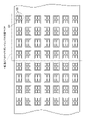
- FIG. 4 is a diagram for explaining an example of a wire bonding target area for each transfer;
- FIG. 10 is a diagram showing an example of display of wire bonding quality inspection results; It is a figure which shows the structure of the test
- the wire bonding apparatus 10 includes, for example, a stage 11, an XY table 12, a bonding head 13, a bonding arm 14, a capillary 15 (an example of a bonding tool), a discharge electrode 16, and a clamper. 17.
- a substrate 51 on which a semiconductor chip 50 is mounted is placed on the stage 11 .
- the stage 11 incorporates a heater (not shown) for heating a lead frame (not shown) formed on the substrate 51 .
- the heater heats the lead frame during wire bonding.
- the XY table 12 is connected to the bonding head 13.
- the bonding head 13 is connected to the bonding arm 14 via an elevating mechanism (not shown).
- the bonding arm 14 is an arm horizontally protruding from the bonding head 13 .
- a capillary 15 is connected to the tip of the bonding arm 14 .
- the capillary 15 moves horizontally with respect to the semiconductor chip 50 mounted on the stage 11 as the bonding head 13 moves horizontally by the XY table 12 and moves vertically by the lifting mechanism. It is configured to be relatively movable in both directions and up and down directions.
- the bonding arm 14 has a built-in ultrasonic transducer.
- the ultrasonic vibrator applies ultrasonic vibration to the capillary 15 connected to the tip of the bonding arm 14 by applying a voltage when wire bonding is performed.
- the capillary 15 faces the stage 11 in the vertical direction, and has a through hole penetrating in the vertical direction.
- a wire 60 such as a gold wire is inserted through the through hole of the capillary 15 .
- a discharge electrode 16 is arranged near the capillary 15 .
- the clamper 17 is provided above the capillary 15 and configured to clamp the wire 60 inserted through the through-hole of the capillary 15 .
- the wire bonding apparatus 10 presses the ball portion 61 formed at the first end of the wire 60 against the semiconductor chip 50 as the voltage is applied to the discharge electrode 16 .
- the wire bonding apparatus 10 moves the capillary 15 to bend the wire 60 so that a part of the wire 60 is attached to the terminal of the substrate 51 . They face each other in the vertical direction.
- the wire bonding apparatus 10 presses the part of the wire 60 against the terminal of the substrate 51 as the voltage is applied to the discharge electrode 16 .
- the wire bonding apparatus 10 cuts the wire 60 by moving the capillary 15 upward while clamping the wire 60 with the clamper 17 . .
- the wire bonding apparatus 10 includes, for example, a control section 110 and a storage section 120.
- the control unit 110 is realized, for example, by a hardware processor such as a CPU (Central Processing Unit) executing a program (software).
- a hardware processor such as a CPU (Central Processing Unit) executing a program (software).
- some or all of these components are hardware (circuit (including circuitry), or by cooperation of software and hardware.
- the program may be stored in advance in a storage device such as an HDD or flash memory of the wire bonding apparatus 10, or may be stored in a removable storage medium such as a DVD or CD-ROM. It may be installed in the HDD or flash memory of the wire bonding apparatus 10 by being attached.
- the storage unit 120 is a nonvolatile storage medium, and is configured by, for example, an HDD (Hard Disk Drive).
- the storage unit 120 stores various parameter values, functions, lookup tables, etc. used for control and calculation, in addition to programs for executing control and processing of the wire bonding apparatus 10 .
- the process information 121 and inspection criteria 122 are examples of parameter values used for control and calculation.
- the process information 121 is information measured when wire bonding is performed.
- the process information 121 includes, for example, information on the diameter of the crimped ball obtained by crimping the wire 60 to the terminal of the semiconductor chip 50 or the terminal of the substrate 51 by wire bonding.
- the information on the crimp ball diameter is information indicating the quality of wire bonding.
- the information about the pressure ball diameter includes, for example, load, US current, spark voltage, spark current, amount of pressing of ball portion 61, and observation information.
- the load is information about the load acting from the capillary 15 to the terminals of the semiconductor chip 50 or the terminals of the substrate 51 when wire bonding is performed.
- the US current is information about the current that flows through the ultrasonic transducer when wire bonding is performed.
- the spark voltage is information about the voltage applied to the discharge electrode 16 during wire bonding.
- the spark current is information about the current flowing through the discharge electrode 16 during wire bonding.
- the amount of pressing of the ball portion 61 is information regarding the amount of pressing of the ball portion 61 at the tip of the wire 60 against the terminal of the semiconductor chip 50 or the terminal of the substrate 51 during wire bonding.
- the observation information includes image information of the crimped portion of the wire 60 with respect to the terminal of the semiconductor chip 50 or the terminal of the substrate 51 .
- the inspection standard 122 is information used when inspecting the quality of wire bonding, and is, for example, a threshold for information on the diameter of the crimped ball.
- the control unit 110 includes, for example, an acquisition unit 111, an inspection unit 112, and a notification unit 113.
- the acquisition unit 111 acquires information about the diameter of the crimped ball to which the wire 60 is crimped by wire bonding to the terminal of the semiconductor chip 50 or the terminal of the substrate 51 . For example, when the acquisition unit 111 acquires information about the crimp ball diameter during wire bonding, the acquisition unit 111 stores the acquired information as the process information 121 in the storage unit 120 .
- the inspection unit 112 inspects the wire bonding quality based on the information on the crimped ball diameter read from the storage unit 120 .
- the inspection unit 112 inspects the quality of wire bonding by referring to the inspection criteria 122 stored in the storage unit 120, for example, based on the information about the crimped ball diameter acquired by the acquisition unit 111.
- FIG. The inspecting unit 112 inspects the quality of wire bonding by comparing, for example, the information about the crimped ball diameter acquired by the acquiring unit 111 with the threshold value stored as the inspection standard 122 in the storage unit 120 .
- the notification unit 113 notifies the wire bonding quality inspection result. For example, when the inspection unit 112 outputs an inspection result indicating that the wire bonding quality is defective, the notification unit 113 notifies the wire bonding quality inspection result by the inspection unit 112 .
- the flowchart shown in FIG. 3 is started, for example, when the user requests confirmation of wire bonding quality.
- the wire bonding apparatus 10 acquires information about the diameter of the crimped ball stored as the process information 121 in the storage unit 120 (step S10).
- the wire bonding apparatus 10 determines whether or not the information on the crimped ball diameter acquired in step S10 satisfies a predetermined condition (step S11).
- the wire bonding apparatus 10 ends the processing of the flowchart shown in FIG. 3 without notifying the wire bonding quality inspection result.
- the wire bonding apparatus 10 notifies the inspection result of the wire bonding quality (step S12), and the flow chart shown in FIG. end the processing of
- control section 110A of the wire bonding apparatus 10A further includes a reference setting section 114 in addition to the acquisition section 111, the inspection section 112, and the notification section 113, for example.
- the standard setting unit 114 sets an inspection standard 122 for the information on the pressure ball diameter when the amount of information on the pressure ball diameter stored as the process information 121 in the storage unit 120A exceeds a predetermined amount.
- the reference setting unit 114 reads, for example, the correlation data 123 indicating the correlation between the amount of pressing of the ball portion 61 and the diameter of the crimping ball from the storage unit 120A, and refers to the read correlation data 123 to determine the amount of pressing of the ball portion 61. is set as the inspection criterion 122 .
- the inspection unit 112 compares the pressing amount of the ball portion 61 acquired by the acquisition unit 111 and the threshold value set as the inspection standard 122 by the standard setting unit 114 to inspect the wire bonding quality.
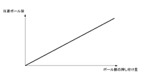
- FIG. 5 shows an example of correlation data 123 indicating the correlation between the amount of pressing of the ball portion 61 and the diameter of the crimped ball. As shown in the figure, there is a positive correlation between the amount of pressing of the ball portion 61 and the diameter of the crimped ball.
- the reference setting unit 114 refers to the correlation data 123 read from the storage unit 120A based on the standard data of the diameter of the crimping ball set in advance, and specifies the pressing amount of the ball portion 61 corresponding to the standard data. , a numerical range including the pressing amount of the specified ball portion 61 is set as the inspection standard 122 .
- the inspection unit 112 inspects the wire bonding quality based on, for example, whether the pressing amount of the ball portion 61 acquired by the acquisition unit 111 is within the numerical range set as the inspection standard 122 .
- the flowchart shown in FIG. 6 is started, for example, each time the process information 121 is acquired.
- the wire bonding apparatus 10A determines whether or not the amount of information regarding the crimping ball diameter is equal to or greater than a predetermined amount (step S20).
- the wire bonding apparatus 10A stores the correlation data 123 indicating the correlation between the pressing amount of the ball portion 61 and the pressure ball diameter in the storage section 120A. (step S21).
- the wire bonding apparatus 10A refers to the correlation data 123 based on the standard data of the pressure-bonding ball diameter, and specifies the pressing amount of the ball portion 61 corresponding to the standard data (step S22).
- the wire bonding apparatus 10A sets the numerical range including the pressing amount of the ball portion 61 specified in the previous step S22 as the inspection standard 122 (step S23), and ends the flowchart shown in FIG.
- step S32 YES
- the wire bonding apparatus 10A does not notify the wire bonding quality inspection result. , terminates the flow chart shown in FIG.
- the notification unit 113 of the wire bonding apparatus 10 reports the wire bonding quality inspection result by the inspection unit 112 in association with the information on the position of the wire bonding at the terminal of the semiconductor chip 50 or the terminal of the substrate 51. inform.
- the wire bonding apparatus 10 performs wire bonding on the substrate 51 while intermittently transporting the substrate 51 .
- a group of substrates 51 arranged side by side in the first direction and the second direction, where the transport direction of the substrates 51 is defined as the first direction and the direction intersecting the transport direction of the substrates 51 is defined as the second direction. is the target area for wire bonding for each transfer.
- FIG. 9 is a diagram showing an example of display of the wire bonding quality inspection result in the wire bonding apparatus 10 according to the third embodiment.
- the notification unit 113 of the wire bonding apparatus 10 notifies the inspection result of the quality of the wire bonding performed for each semiconductor chip 50 to the position of the substrate 51 on which each semiconductor chip 50 is mounted. are displayed on the display unit 200 in association with each other.
- the notification unit 113 of the wire bonding apparatus 10 displays the wire bonding quality inspection results performed for each semiconductor chip 50 in descending order of wire bonding quality: "standard”, "warning", and "warning". It is displayed on the display unit 200 as "abnormal".
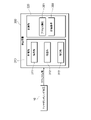
- an inspection apparatus 300 includes, for example, a control section 310 and a storage section 320. As shown in FIG. 10, an inspection apparatus 300 according to the fourth embodiment includes, for example, a control section 310 and a storage section 320. As shown in FIG. 10,
- the control unit 310 is implemented, for example, by a hardware processor such as a CPU (Central Processing Unit) executing a program (software). In addition, some or all of these components are hardware (circuit (including circuitry), or by cooperation of software and hardware.
- the program may be stored in advance in a storage device such as the HDD or flash memory of the inspection device 300, or may be stored in a removable storage medium such as a DVD or CD-ROM. It may be installed in the HDD or flash memory of the inspection apparatus 300 by being installed.
- the storage unit 320 is a non-volatile storage medium, and is configured by, for example, an HDD (Hard Disk Drive).
- the storage unit 320 stores various parameter values, functions, lookup tables, etc. used for control and calculation, in addition to programs for executing control and processing of the inspection apparatus 300 .
- Process information 321 and inspection criteria 322 are examples of parameter values used for control and calculation.
- the control unit 310 includes, for example, an acquisition unit 311, an inspection unit 312, and a notification unit 313.
- the acquisition unit 311 acquires from the wire bonding apparatus 10 information about the diameter of the crimped ball to which the wire 60 is crimped to the terminal of the semiconductor chip 50 or the terminal of the substrate 51 by wire bonding. For example, when acquiring information about the crimp ball diameter from the wire bonding apparatus 10 during execution of wire bonding, the acquisition unit 311 stores the acquired information in the storage unit 320 as process information 321 .
- the inspection unit 312 inspects the wire bonding quality based on the information on the crimped ball diameter read from the storage unit 320 .
- the inspection unit 312 inspects the wire bonding quality by referring to the inspection criteria 322 stored in the storage unit 320 based on the information on the crimped ball diameter acquired by the acquisition unit 311, for example.
- the inspecting unit 312 inspects the quality of wire bonding by comparing, for example, the information on the crimped ball diameter acquired by the acquiring unit 311 with the threshold value stored as the inspection criteria 322 in the storage unit 320 .
- the notification unit 313 notifies the wire bonding quality inspection result. For example, when the inspection unit 312 outputs an inspection result indicating that the wire bonding quality is defective, the notification unit 313 notifies the inspection result of the wire bonding quality by the inspection unit 312 .
- the inspection standard 122 does not necessarily have to be a numerical range including the pressing amount of the ball portion 61 specified based on the preset standard data of the pressure-bonded ball diameter. It may be a numerical range including the pressing amount of the ball portion 61 specified based on the statistical data of the pressure-bonded ball diameter acquired by 111 . Further, the inspection standard 122 may be a numerical range higher than the pressing amount of the ball portion 61 specified as described above or a numerical range lower than the pressing amount of the ball portion 61 specified as described above. Also, the inspection standard 122 does not necessarily have to be a numerical range. may be a combination of
- the correlation data 123 does not necessarily have to be data indicating the correlation between the amount of pressing of the ball portion 61 and the diameter of the crimped ball. If the quality is to be inspected, the correlation data 123 may be data indicating the correlation between the spark voltage and the pressure-bonded ball diameter.
- the functional block configuration included in the wire bonding apparatuses 10 and 10A may be configured as a wire bonding system distributed between the wire bonding apparatuses 10 and 10A and an external apparatus. good.
- the wire bonding apparatus according to each of the above embodiments has been described by taking as an example the case where the terminals of the semiconductor chip 50 and the terminals of the substrate 51 are electrically connected by the wires 60 .
- the wire bonding apparatus according to each of the above-described embodiments can be applied, for example, to the case of configuring a semiconductor module by electrically connecting the terminals of the semiconductor chip 50 and the terminals of the lead frame with the wires 60. is.
- the wire bonding apparatus according to each of the above-described embodiments can also be applied to forming bumps on arbitrary electrodes such as terminals of the semiconductor chip 50 by the wires 60, for example.
- Reference Signs List 10 10A Wire bonding apparatus 11 Stage 12 XY table 13 Bonding head 14 Bonding arm 15 Capillary 16 Discharge electrode 17 Clamper 50 Semiconductor chip 51 Substrate 60 ... wire 61 ... ball section 110, 110A, 310 ... control section 111, 311 ... acquisition section 112, 312 ... inspection section 113, 313 ... notification section 114 ... reference setting section 120, 120A, 320 ... Memory unit 121, 321 Process information 122 Inspection standard 123 Correlation data 200 Display unit 300 Inspection device 322 Inspection standard.
Landscapes
- Engineering & Computer Science (AREA)
- Mechanical Engineering (AREA)
- Quality & Reliability (AREA)
- Wire Bonding (AREA)
Abstract
Description
以下、図面を参照して、第1実施形態に係るワイヤボンディング装置について説明する。
第2実施形態以降では第1実施形態と共通の事柄についての記述を省略し、異なる点についてのみ説明する。特に、同様の構成による同様の作用効果については実施形態毎には逐次言及しない。
第3実施形態に係るワイヤボンディング装置10の報知部113は、半導体チップ50の端子または基板51の端子におけるワイヤボンディングの位置に関する情報と対応付けて、検査部112によるワイヤボンディングの品質の検査結果を報知する。
図10に示すように、第4実施形態に係る検査装置300は、例えば、制御部310と、記憶部320とを備える。
Claims (10)
- 電子部品に対してワイヤボンディングによりワイヤが圧着された圧着ボール径に関する情報を取得する取得部と、
前記取得部により取得した前記圧着ボール径に関する情報を記憶する第1記憶部と、
前記第1記憶部から読み出した前記圧着ボール径に関する情報に基づいて、ワイヤボンディングの品質を検査する検査部と、
を備える、
ワイヤボンディングシステム。 - 前記検査部によるワイヤボンディングの品質の検査結果が所定条件を満たさない場合、ワイヤボンディングの品質の検査結果を報知する報知部をさらに備える、
請求項1に記載のワイヤボンディングシステム。 - 前記報知部は、前記電子部品におけるワイヤボンディングの位置に関する情報と対応付けて、前記検査部によるワイヤボンディングの品質の検査結果を報知する、
請求項2に記載のワイヤボンディングシステム。 - 前記圧着ボール径に関する情報についての検査基準を設定する基準設定部をさらに備え、
前記検査部は、前記取得部により取得した前記圧着ボール径に関する情報に基づいて、前記基準設定部により設定された検査基準を参照して、前記ワイヤボンディングの品質を検査する、
請求項1から3のいずれか一項に記載のワイヤボンディングシステム。 - 前記基準設定部は、前記第1記憶部に記憶された前記圧着ボール径に関する情報の情報量が所定量以上となった場合、前記圧着ボール径に関する情報についての検査基準を設定する、
請求項4に記載のワイヤボンディングシステム。 - 前記圧着ボール径に関する情報は、ワイヤボンディング時における前記電子部品に対するワイヤの先端のボール部の押し付け量を含み、
前記ボール部の押し付け量と前記圧着ボール径との相関を示す相関データを記憶する第2記憶部と、
をさらに備え、
前記基準設定部は、予め設定された前記圧着ボール径の標準データに基づいて、前記第2記憶部から読み出した前記相関データを参照して、前記ボール部の押し付け量についての閾値を前記検査基準として設定し、
前記検査部は、前記取得部により取得した前記ボール部の押し付け量と前記基準設定部により設定された閾値とを比較して、ワイヤボンディングの品質を検査する、
請求項4または5に記載のワイヤボンディングシステム。 - 前記基準設定部は、予め設定された前記圧着ボール径の標準データに基づいて、前記第2記憶部から読み出した前記相関データを参照して、前記標準データに対応する前記ボール部の押し付け量を特定し、前記特定したボール部の押し付け量を含む数値範囲を前記検査基準として設定し、
前記検査部は、前記取得部により取得した前記ボール部の押し付け量が前記検査基準として設定された数値範囲内にあるか否かに基づいて、前記ワイヤボンディングの品質を検査する、
請求項6に記載のワイヤボンディングシステム。 - ワイヤボンディングにより電子部品に対してワイヤが圧着された圧着ボール径に関する情報を第1記憶部から読み出し、前記読み出した圧着ボール径に関する情報に基づいて、前記ワイヤボンディングの品質を検査する検査部を備える、
検査装置。 - 電子部品に対してワイヤボンディングによりワイヤが圧着された圧着ボール径に関する情報を取得する工程と、
前記取得した圧着ボール径に関する情報を第1記憶部に記憶する工程と、
前記第1記憶部から読み出した前記圧着ボール径に関する情報に基づいて、前記ワイヤボンディングの品質を検査する工程と、
を含む、
ワイヤボンディング方法。 - 一又は複数のコンピュータに、
電子部品に対してワイヤボンディングによりワイヤが圧着された圧着ボール径に関する情報を取得する処理と、
前記取得した圧着ボール径に関する情報を第1記憶部に記憶する処理と、
前記第1記憶部から読み出した圧着ボール径に関する情報に基づいて、前記ワイヤボンディングの品質を検査する処理と、
を実行させる、
プログラム。
Priority Applications (5)
| Application Number | Priority Date | Filing Date | Title |
|---|---|---|---|
| JP2023523743A JP7612249B2 (ja) | 2021-05-25 | 2021-05-25 | ワイヤボンディングシステム、検査装置、ワイヤボンディング方法、および、プログラム |
| CN202180094265.0A CN116888715A (zh) | 2021-05-25 | 2021-05-25 | 打线接合系统、检查装置、打线接合方法以及程序 |
| US18/559,342 US12489003B2 (en) | 2021-05-25 | 2021-05-25 | Wire bonding system, inspection device, wire bonding method, and recording medium |
| PCT/JP2021/019712 WO2022249262A1 (ja) | 2021-05-25 | 2021-05-25 | ワイヤボンディングシステム、検査装置、ワイヤボンディング方法、および、プログラム |
| KR1020237027641A KR102891276B1 (ko) | 2021-05-25 | 2021-05-25 | 와이어 본딩 시스템, 검사 장치, 와이어 본딩 방법, 및 기록 매체 |
Applications Claiming Priority (1)
| Application Number | Priority Date | Filing Date | Title |
|---|---|---|---|
| PCT/JP2021/019712 WO2022249262A1 (ja) | 2021-05-25 | 2021-05-25 | ワイヤボンディングシステム、検査装置、ワイヤボンディング方法、および、プログラム |
Publications (1)
| Publication Number | Publication Date |
|---|---|
| WO2022249262A1 true WO2022249262A1 (ja) | 2022-12-01 |
Family
ID=84229759
Family Applications (1)
| Application Number | Title | Priority Date | Filing Date |
|---|---|---|---|
| PCT/JP2021/019712 Ceased WO2022249262A1 (ja) | 2021-05-25 | 2021-05-25 | ワイヤボンディングシステム、検査装置、ワイヤボンディング方法、および、プログラム |
Country Status (5)
| Country | Link |
|---|---|
| US (1) | US12489003B2 (ja) |
| JP (1) | JP7612249B2 (ja) |
| KR (1) | KR102891276B1 (ja) |
| CN (1) | CN116888715A (ja) |
| WO (1) | WO2022249262A1 (ja) |
Cited By (1)
| Publication number | Priority date | Publication date | Assignee | Title |
|---|---|---|---|---|
| US12489003B2 (en) * | 2021-05-25 | 2025-12-02 | Yamaha Robotics Co., Ltd. | Wire bonding system, inspection device, wire bonding method, and recording medium |
Citations (9)
| Publication number | Priority date | Publication date | Assignee | Title |
|---|---|---|---|---|
| JPH0737926A (ja) * | 1993-07-16 | 1995-02-07 | Kaijo Corp | ワイヤボンディング装置及びその方法 |
| JPH07321132A (ja) * | 1994-05-19 | 1995-12-08 | Rohm Co Ltd | 半導体装置の製造方法 |
| JPH0864629A (ja) * | 1994-08-25 | 1996-03-08 | Toshiba Seiki Kk | ワイヤボンディング方法 |
| JPH09189531A (ja) * | 1996-01-09 | 1997-07-22 | Rohm Co Ltd | 半導体レーザのワイヤの検査方法 |
| JPH10199915A (ja) * | 1997-01-07 | 1998-07-31 | Kaijo Corp | ワイヤーボンディング方法およびその装置 |
| JP2001118880A (ja) * | 1999-10-18 | 2001-04-27 | Matsushita Electric Ind Co Ltd | ワイヤボンデイングにおけるファーストボンディング点の検査方法 |
| JP2004186591A (ja) * | 2002-12-05 | 2004-07-02 | Shinko Electric Ind Co Ltd | 配線検証システム |
| JP2006186087A (ja) * | 2004-12-27 | 2006-07-13 | Shinkawa Ltd | ボンディング装置 |
| WO2015122411A1 (ja) * | 2014-02-17 | 2015-08-20 | 株式会社新川 | 放電検査装置、ワイヤボンディング装置、および放電検査方法 |
Family Cites Families (28)
| Publication number | Priority date | Publication date | Assignee | Title |
|---|---|---|---|---|
| KR940005715B1 (ko) * | 1991-11-18 | 1994-06-23 | 삼성전자 주식회사 | 본딩와이어의 높이판단 장치를 구비한 반도체 와이어본딩 장치 |
| JPH05335389A (ja) * | 1992-06-03 | 1993-12-17 | Fujitsu Ltd | ボンディングワイヤ検査装置 |
| JP2914850B2 (ja) * | 1993-07-16 | 1999-07-05 | 株式会社カイジョー | ワイヤボンディング装置及びその方法 |
| JP2992427B2 (ja) * | 1993-07-16 | 1999-12-20 | 株式会社カイジョー | ワイヤボンディング装置及びその方法 |
| JP3009564B2 (ja) * | 1993-07-16 | 2000-02-14 | 株式会社カイジョー | ワイヤボンディング装置及びその方法 |
| JP3235008B2 (ja) * | 1994-07-16 | 2001-12-04 | 株式会社新川 | ワイヤボンデイング部のボール検出方法及び検出装置 |
| JP3414967B2 (ja) * | 1997-02-24 | 2003-06-09 | 松下電器産業株式会社 | バンプ検査方法 |
| JPH1163928A (ja) * | 1997-08-21 | 1999-03-05 | Canon Inc | ボンディングワイヤ検査方法および装置 |
| JPH11297747A (ja) * | 1998-04-14 | 1999-10-29 | Hitachi Ltd | ワイヤボンディング装置およびそれを用いた外観検査方法 |
| JP2002026085A (ja) * | 2000-07-11 | 2002-01-25 | Mitsubishi Electric Corp | 半導体デバイスの組み立て工程検査装置及び検査方法 |
| JP4234661B2 (ja) * | 2004-09-30 | 2009-03-04 | 株式会社カイジョー | ワイヤボンディングにおけるボールの検査方法 |
| JP2006303117A (ja) * | 2005-04-19 | 2006-11-02 | Nec Electronics Corp | ワイヤーボンディング装置 |
| JP4247299B1 (ja) * | 2008-03-31 | 2009-04-02 | 株式会社新川 | ボンディング装置及びボンディング方法 |
| JP4264458B1 (ja) * | 2008-06-13 | 2009-05-20 | 株式会社新川 | 圧着ボール径検出装置および方法 |
| KR101236795B1 (ko) * | 2010-03-29 | 2013-02-25 | 앰코 테크놀로지 코리아 주식회사 | 반도체 패키지 제조용 와이어 본더의 바값 측정 시스템 |
| KR101121443B1 (ko) * | 2010-04-26 | 2012-03-16 | 주식회사 미라콤아이앤씨 | 와이어본딩 프로세스에서의 오류 자동 검출 방법, 시스템, 및 저장 매체 |
| US8907485B2 (en) * | 2012-08-24 | 2014-12-09 | Freescale Semiconductor, Inc. | Copper ball bond features and structure |
| CN104241154B (zh) * | 2013-06-14 | 2017-02-22 | 无锡华润安盛科技有限公司 | 倒装芯片焊点润湿性的判定方法及其芯片的焊接方法 |
| US10121759B2 (en) * | 2015-11-04 | 2018-11-06 | Kulicke And Soffa Industries, Inc. | On-bonder automatic overhang die optimization tool for wire bonding and related methods |
| JP2017216314A (ja) * | 2016-05-31 | 2017-12-07 | 株式会社新川 | ボンディング装置、ボンディング方法及びプログラム |
| WO2018110417A1 (ja) * | 2016-12-14 | 2018-06-21 | 株式会社新川 | ワイヤボンディング装置及びワイヤボンディング方法 |
| JP6869920B2 (ja) * | 2018-04-02 | 2021-05-12 | 田中電子工業株式会社 | ボールボンディング用貴金属被覆銀ワイヤおよびその製造方法、ならびにボールボンディング用貴金属被覆銀ワイヤを使用した半導体装置およびその製造方法 |
| JP6487108B1 (ja) * | 2018-11-26 | 2019-03-20 | 田中電子工業株式会社 | パラジウム被覆銅ボンディングワイヤ及びその製造方法 |
| JP7316796B2 (ja) | 2019-01-23 | 2023-07-28 | 三菱電機株式会社 | ワイヤボンディング装置、ワイヤボンディング方法および半導体装置の製造方法 |
| CN113748493B (zh) * | 2019-03-12 | 2025-03-21 | 田中电子工业株式会社 | 钯覆盖铜接合线、钯覆盖铜接合线的制造方法、及使用了其的引线接合结构、半导体装置以及其制造方法 |
| TWI732506B (zh) * | 2019-04-22 | 2021-07-01 | 日商新川股份有限公司 | 線形狀測量裝置、線三維圖像產生方法以及線形狀測量方法 |
| US12489003B2 (en) * | 2021-05-25 | 2025-12-02 | Yamaha Robotics Co., Ltd. | Wire bonding system, inspection device, wire bonding method, and recording medium |
| CN114420580A (zh) * | 2022-01-20 | 2022-04-29 | 无锡嘉硕科技有限公司 | 一种防止打线后球薄的方法 |
-
2021
- 2021-05-25 US US18/559,342 patent/US12489003B2/en active Active
- 2021-05-25 JP JP2023523743A patent/JP7612249B2/ja active Active
- 2021-05-25 CN CN202180094265.0A patent/CN116888715A/zh active Pending
- 2021-05-25 WO PCT/JP2021/019712 patent/WO2022249262A1/ja not_active Ceased
- 2021-05-25 KR KR1020237027641A patent/KR102891276B1/ko active Active
Patent Citations (9)
| Publication number | Priority date | Publication date | Assignee | Title |
|---|---|---|---|---|
| JPH0737926A (ja) * | 1993-07-16 | 1995-02-07 | Kaijo Corp | ワイヤボンディング装置及びその方法 |
| JPH07321132A (ja) * | 1994-05-19 | 1995-12-08 | Rohm Co Ltd | 半導体装置の製造方法 |
| JPH0864629A (ja) * | 1994-08-25 | 1996-03-08 | Toshiba Seiki Kk | ワイヤボンディング方法 |
| JPH09189531A (ja) * | 1996-01-09 | 1997-07-22 | Rohm Co Ltd | 半導体レーザのワイヤの検査方法 |
| JPH10199915A (ja) * | 1997-01-07 | 1998-07-31 | Kaijo Corp | ワイヤーボンディング方法およびその装置 |
| JP2001118880A (ja) * | 1999-10-18 | 2001-04-27 | Matsushita Electric Ind Co Ltd | ワイヤボンデイングにおけるファーストボンディング点の検査方法 |
| JP2004186591A (ja) * | 2002-12-05 | 2004-07-02 | Shinko Electric Ind Co Ltd | 配線検証システム |
| JP2006186087A (ja) * | 2004-12-27 | 2006-07-13 | Shinkawa Ltd | ボンディング装置 |
| WO2015122411A1 (ja) * | 2014-02-17 | 2015-08-20 | 株式会社新川 | 放電検査装置、ワイヤボンディング装置、および放電検査方法 |
Cited By (1)
| Publication number | Priority date | Publication date | Assignee | Title |
|---|---|---|---|---|
| US12489003B2 (en) * | 2021-05-25 | 2025-12-02 | Yamaha Robotics Co., Ltd. | Wire bonding system, inspection device, wire bonding method, and recording medium |
Also Published As
| Publication number | Publication date |
|---|---|
| US20240242984A1 (en) | 2024-07-18 |
| JPWO2022249262A1 (ja) | 2022-12-01 |
| CN116888715A (zh) | 2023-10-13 |
| JP7612249B2 (ja) | 2025-01-14 |
| US12489003B2 (en) | 2025-12-02 |
| KR102891276B1 (ko) | 2025-12-03 |
| KR20230132535A (ko) | 2023-09-15 |
Similar Documents
| Publication | Publication Date | Title |
|---|---|---|
| JP5918205B2 (ja) | 試験装置及びその試験方法 | |
| JPS59134841A (ja) | 電子部品へのボンデイングのためのオン・ライン検査方法およびシステム | |
| US8496158B2 (en) | Method and apparatus for monitoring free air ball (FAB) formation in wire bonding | |
| US6237833B1 (en) | Method of checking wirebond condition | |
| JP7612249B2 (ja) | ワイヤボンディングシステム、検査装置、ワイヤボンディング方法、および、プログラム | |
| CN106463423B (zh) | 放电检查装置、打线装置以及放电检查方法 | |
| CN108231619A (zh) | 用于功率半导体芯片的检测方法 | |
| CN205484688U (zh) | 芯片失效分析仪 | |
| JP2008026336A (ja) | コンタクタ | |
| TWI848292B (zh) | 打線接合系統、打線接合檢查裝置、打線接合方法以及電腦程式產品 | |
| CN119492980A (zh) | 键合引线的可靠性评估方法 | |
| CN205484687U (zh) | 通用型芯片失效分析的测试装置 | |
| JP4471746B2 (ja) | 半導体実装方法 | |
| JP3573113B2 (ja) | ボンディングダメージの計測装置および計測方法 | |
| CN115343657B (zh) | 键合材料的熔断电流测试板、系统、方法及装置 | |
| WO2022249243A1 (ja) | ワイヤボンディング装置、メンテナンス方法、および、プログラム | |
| CN101488482A (zh) | 半导体封装结构及其制造方法 | |
| JP5195456B2 (ja) | ソケット、半導体装置及びソケットの信頼性評価方法 | |
| JP5126009B2 (ja) | 試験方法、試験装置及び半導体装置の製造方法 | |
| JP2000346897A (ja) | パッド導通検査装置 | |
| JP2011114161A (ja) | 半導体装置、半導体装置の製造方法および半導体装置の判別方法 | |
| JP2025062175A (ja) | 半導体製造装置 | |
| CN120446719A (zh) | 芯片的测试方法、测试装置以及存储介质 | |
| JP5389541B2 (ja) | 基板検査装置 | |
| TW202536983A (zh) | 導線接合裝置、控制裝置及控制方法 |
Legal Events
| Date | Code | Title | Description |
|---|---|---|---|
| 121 | Ep: the epo has been informed by wipo that ep was designated in this application |
Ref document number: 21942918 Country of ref document: EP Kind code of ref document: A1 |
|
| ENP | Entry into the national phase |
Ref document number: 20237027641 Country of ref document: KR Kind code of ref document: A |
|
| WWE | Wipo information: entry into national phase |
Ref document number: 1020237027641 Country of ref document: KR |
|
| WWE | Wipo information: entry into national phase |
Ref document number: 202180094265.0 Country of ref document: CN |
|
| WWE | Wipo information: entry into national phase |
Ref document number: 11202306081P Country of ref document: SG |
|
| WWE | Wipo information: entry into national phase |
Ref document number: 18559342 Country of ref document: US |
|
| WWE | Wipo information: entry into national phase |
Ref document number: 2023523743 Country of ref document: JP |
|
| NENP | Non-entry into the national phase |
Ref country code: DE |
|
| 122 | Ep: pct application non-entry in european phase |
Ref document number: 21942918 Country of ref document: EP Kind code of ref document: A1 |