WO2022234656A1 - 半導体素子を有するメモリ装置 - Google Patents
半導体素子を有するメモリ装置 Download PDFInfo
- Publication number
- WO2022234656A1 WO2022234656A1 PCT/JP2021/017504 JP2021017504W WO2022234656A1 WO 2022234656 A1 WO2022234656 A1 WO 2022234656A1 JP 2021017504 W JP2021017504 W JP 2021017504W WO 2022234656 A1 WO2022234656 A1 WO 2022234656A1
- Authority
- WO
- WIPO (PCT)
- Prior art keywords
- layer
- semiconductor
- conductor layer
- gate conductor
- line
- Prior art date
- Legal status (The legal status is an assumption and is not a legal conclusion. Google has not performed a legal analysis and makes no representation as to the accuracy of the status listed.)
- Ceased
Links
Images






Classifications
-
- G—PHYSICS
- G11—INFORMATION STORAGE
- G11C—STATIC STORES
- G11C5/00—Details of stores covered by group G11C11/00
- G11C5/02—Disposition of storage elements, e.g. in the form of a matrix array
- G11C5/025—Geometric lay-out considerations of storage- and peripheral-blocks in a semiconductor storage device
-
- G—PHYSICS
- G11—INFORMATION STORAGE
- G11C—STATIC STORES
- G11C11/00—Digital stores characterised by the use of particular electric or magnetic storage elements; Storage elements therefor
- G11C11/21—Digital stores characterised by the use of particular electric or magnetic storage elements; Storage elements therefor using electric elements
- G11C11/34—Digital stores characterised by the use of particular electric or magnetic storage elements; Storage elements therefor using electric elements using semiconductor devices
- G11C11/40—Digital stores characterised by the use of particular electric or magnetic storage elements; Storage elements therefor using electric elements using semiconductor devices using transistors
- G11C11/401—Digital stores characterised by the use of particular electric or magnetic storage elements; Storage elements therefor using electric elements using semiconductor devices using transistors forming cells needing refreshing or charge regeneration, i.e. dynamic cells
- G11C11/403—Digital stores characterised by the use of particular electric or magnetic storage elements; Storage elements therefor using electric elements using semiconductor devices using transistors forming cells needing refreshing or charge regeneration, i.e. dynamic cells with charge regeneration common to a multiplicity of memory cells, i.e. external refresh
- G11C11/404—Digital stores characterised by the use of particular electric or magnetic storage elements; Storage elements therefor using electric elements using semiconductor devices using transistors forming cells needing refreshing or charge regeneration, i.e. dynamic cells with charge regeneration common to a multiplicity of memory cells, i.e. external refresh with one charge-transfer gate, e.g. MOS transistor, per cell
-
- G—PHYSICS
- G11—INFORMATION STORAGE
- G11C—STATIC STORES
- G11C11/00—Digital stores characterised by the use of particular electric or magnetic storage elements; Storage elements therefor
- G11C11/21—Digital stores characterised by the use of particular electric or magnetic storage elements; Storage elements therefor using electric elements
- G11C11/34—Digital stores characterised by the use of particular electric or magnetic storage elements; Storage elements therefor using electric elements using semiconductor devices
- G11C11/40—Digital stores characterised by the use of particular electric or magnetic storage elements; Storage elements therefor using electric elements using semiconductor devices using transistors
- G11C11/401—Digital stores characterised by the use of particular electric or magnetic storage elements; Storage elements therefor using electric elements using semiconductor devices using transistors forming cells needing refreshing or charge regeneration, i.e. dynamic cells
- G11C11/4063—Auxiliary circuits, e.g. for addressing, decoding, driving, writing, sensing or timing
- G11C11/407—Auxiliary circuits, e.g. for addressing, decoding, driving, writing, sensing or timing for memory cells of the field-effect type
- G11C11/409—Read-write [R-W] circuits
- G11C11/4094—Bit-line management or control circuits
-
- G—PHYSICS
- G11—INFORMATION STORAGE
- G11C—STATIC STORES
- G11C11/00—Digital stores characterised by the use of particular electric or magnetic storage elements; Storage elements therefor
- G11C11/21—Digital stores characterised by the use of particular electric or magnetic storage elements; Storage elements therefor using electric elements
- G11C11/34—Digital stores characterised by the use of particular electric or magnetic storage elements; Storage elements therefor using electric elements using semiconductor devices
- G11C11/40—Digital stores characterised by the use of particular electric or magnetic storage elements; Storage elements therefor using electric elements using semiconductor devices using transistors
- G11C11/401—Digital stores characterised by the use of particular electric or magnetic storage elements; Storage elements therefor using electric elements using semiconductor devices using transistors forming cells needing refreshing or charge regeneration, i.e. dynamic cells
- G11C11/4063—Auxiliary circuits, e.g. for addressing, decoding, driving, writing, sensing or timing
- G11C11/407—Auxiliary circuits, e.g. for addressing, decoding, driving, writing, sensing or timing for memory cells of the field-effect type
- G11C11/409—Read-write [R-W] circuits
- G11C11/4096—Input/output [I/O] data management or control circuits, e.g. reading or writing circuits, I/O drivers or bit-line switches
-
- G—PHYSICS
- G11—INFORMATION STORAGE
- G11C—STATIC STORES
- G11C11/00—Digital stores characterised by the use of particular electric or magnetic storage elements; Storage elements therefor
- G11C11/21—Digital stores characterised by the use of particular electric or magnetic storage elements; Storage elements therefor using electric elements
- G11C11/34—Digital stores characterised by the use of particular electric or magnetic storage elements; Storage elements therefor using electric elements using semiconductor devices
- G11C11/40—Digital stores characterised by the use of particular electric or magnetic storage elements; Storage elements therefor using electric elements using semiconductor devices using transistors
- G11C11/401—Digital stores characterised by the use of particular electric or magnetic storage elements; Storage elements therefor using electric elements using semiconductor devices using transistors forming cells needing refreshing or charge regeneration, i.e. dynamic cells
- G11C11/4063—Auxiliary circuits, e.g. for addressing, decoding, driving, writing, sensing or timing
- G11C11/407—Auxiliary circuits, e.g. for addressing, decoding, driving, writing, sensing or timing for memory cells of the field-effect type
- G11C11/409—Read-write [R-W] circuits
- G11C11/4097—Bit-line organisation, e.g. bit-line layout, folded bit lines
-
- G—PHYSICS
- G11—INFORMATION STORAGE
- G11C—STATIC STORES
- G11C11/00—Digital stores characterised by the use of particular electric or magnetic storage elements; Storage elements therefor
- G11C11/21—Digital stores characterised by the use of particular electric or magnetic storage elements; Storage elements therefor using electric elements
- G11C11/34—Digital stores characterised by the use of particular electric or magnetic storage elements; Storage elements therefor using electric elements using semiconductor devices
- G11C11/40—Digital stores characterised by the use of particular electric or magnetic storage elements; Storage elements therefor using electric elements using semiconductor devices using transistors
- G11C11/41—Digital stores characterised by the use of particular electric or magnetic storage elements; Storage elements therefor using electric elements using semiconductor devices using transistors forming static cells with positive feedback, i.e. cells not needing refreshing or charge regeneration, e.g. bistable multivibrator or Schmitt trigger
- G11C11/412—Digital stores characterised by the use of particular electric or magnetic storage elements; Storage elements therefor using electric elements using semiconductor devices using transistors forming static cells with positive feedback, i.e. cells not needing refreshing or charge regeneration, e.g. bistable multivibrator or Schmitt trigger using field-effect transistors only
-
- G—PHYSICS
- G11—INFORMATION STORAGE
- G11C—STATIC STORES
- G11C7/00—Arrangements for writing information into, or reading information out from, a digital store
- G11C7/02—Arrangements for writing information into, or reading information out from, a digital store with means for avoiding parasitic signals
-
- H—ELECTRICITY
- H10—SEMICONDUCTOR DEVICES; ELECTRIC SOLID-STATE DEVICES NOT OTHERWISE PROVIDED FOR
- H10B—ELECTRONIC MEMORY DEVICES
- H10B12/00—Dynamic random access memory [DRAM] devices
- H10B12/20—DRAM devices comprising floating-body transistors, e.g. floating-body cells
-
- G—PHYSICS
- G11—INFORMATION STORAGE
- G11C—STATIC STORES
- G11C2211/00—Indexing scheme relating to digital stores characterized by the use of particular electric or magnetic storage elements; Storage elements therefor
- G11C2211/401—Indexing scheme relating to cells needing refreshing or charge regeneration, i.e. dynamic cells
- G11C2211/4016—Memory devices with silicon-on-insulator cells
Definitions
- the present invention relates to a memory device having semiconductor elements.
- the channel In a normal planar MOS transistor, the channel extends horizontally along the upper surface of the semiconductor substrate. In contrast, the SGT channel extends in a direction perpendicular to the upper surface of the semiconductor substrate (see Patent Document 1 and Non-Patent Document 1, for example). For this reason, the SGT enables a higher density semiconductor device compared to a planar MOS transistor.
- a DRAM Dynamic Random Access Memory
- a PCM Phase Change Memory
- Non-Patent Document 4 RRAM (Resistive Random Access Memory, see, for example, Non-Patent Document 4), MRAM (Magneto-resistive Random Access Memory, see, for example, Non-Patent Document 5) that changes the resistance by changing the direction of the magnetic spin by current ) can be highly integrated.
- DRAM memory cell see Non-Patent Document 6
- the present application relates to a semiconductor device having a dynamic flash memory that does not have resistance change elements or capacitors and can be configured only with MOS transistors.
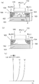
- FIG. 9 shows the write operation of a DRAM memory cell composed of a single MOS transistor without the capacitor described above
- FIG. 10 shows the problem in operation
- FIG. 9 shows the write operation of the DRAM memory cell.
- FIG. 9(a) shows a "1" write state.
- the memory cell is formed on the SOI substrate 101 and includes a source N + layer 103 (hereinafter, a semiconductor region containing a high concentration of donor impurities is referred to as an “N + layer”) to which a source line SL is connected, a bit line It is composed of a drain N + layer 104 to which BL is connected, a gate conductive layer 105 to which word line WL is connected, and a floating body 102 of MOS transistor 110a. constitutes a DRAM memory cell.
- the SiO 2 layer 101 of the SOI substrate is in contact directly below the floating body 102 .
- the MOS transistor 110a When "1" is written to the memory cell constituted by one MOS transistor 110a, the MOS transistor 110a is operated in the linear region. That is, the electron channel 107 extending from the source N + layer 103 has a pinch-off point 108 and does not reach the drain N + layer 104 connected to the bit line. In this way, both the bit line BL connected to the drain N + layer 104 and the word line WL connected to the gate conductive layer 105 are set at a high voltage, and the gate voltage is set to about 1/2 of the drain voltage. , the electric field strength is maximized at the pinch-off point 108 near the drain N + layer 104 .
- the holes 106 generated at the same time charge the floating body 102 . In this case, the generated holes contribute as increments of majority carriers because the floating body 102 is P-type Si.
- the floating body 102 is filled with the generated holes 106, and when the voltage of the floating body 102 becomes higher than that of the source N + layer 103 by Vb or more, the generated holes are discharged to the source N + layer 103.
- Vb is the built-in voltage of the PN junction between the source N + layer 103 and the floating body 102 of the P layer, which is about 0.7V.
- FIG. 9B shows the floating body 102 saturated with the generated holes 106 .
- FIG. 9(c) shows how the "1" write state is rewritten to the "0" write state.
- the voltage of the bit line BL is negatively biased, and the PN junction between the drain N + layer 104 and the floating body 102 of the P layer is forward biased.
- the holes 106 previously generated in the floating body 102 in the previous cycle flow to the drain N + layer 104 connected to the bit line BL.
- FIG. 9(b) filled with the generated holes 106 and 110b (FIG. 9(c)) from which the generated holes are ejected are stored.
- the state of the memory cell is obtained.
- the floating body 102 potential of the memory cell 110a filled with holes 106 will be higher than the floating body 102 without the generated holes. Therefore, the threshold voltage of memory cell 110a is lower than that of memory cell 110b. This state is shown in FIG. 9(d).
- ⁇ 0.8.
- FIG. FIG. 11(a) shows a "1" write state
- FIG. 11(b) shows a "0" write state.
- Vb the floating body 102
- the floating body 102 is pulled down to a negative bias when the word line returns to 0 V at the end of writing.
- the potential difference margin between "1” and “0” cannot be made sufficiently large because the negative bias becomes even deeper.
- This small operating margin is a major problem of the present DRAM memory cell.
- the problem is how to form peripheral circuits for driving the DRAM memory cells on the same substrate.
- Critoloveanu “A Compact Capacitor-Less High-Speed DRAM Using Field Effect-Controlled Charge Regeneration,” Electron Device Letters, Vol. 35, No.2, pp. 179-181 (2012) T. Ohsawa, K. Fujita, T. Higashi, Y. Iwata, T. Kajiyama, Y. Asao, and K. Sunouchi: “Memory design using a one-transistor gain cell on SOI,” IEEE JSSC, vol.37, No.11, pp1510-1522 (2002). T. Shino, N. Kusunoki, T. Higashi, T. Ohsawa, K. Fujita, K. Hatsuda, N. Ikumi, F.
- a memory device using a columnar semiconductor element includes: A first semiconductor pillar and a second semiconductor pillar which stand vertically on a substrate, have a center point on a first line in a plan view, are arranged adjacent to each other, and are parallel to the first line.
- a third semiconductor pillar and a fourth semiconductor pillar having a center point on the second line and arranged adjacent to each other; a first impurity region connected to the bottoms of the first to fourth semiconductor pillars; a first gate insulating layer vertically above the first impurity region and surrounding the lower portions of the first to fourth semiconductor pillars; a first gate conductor layer surrounding the first gate insulating layer and surrounding and connecting the first semiconductor pillar and the second semiconductor pillar; the third semiconductor pillar and the fourth semiconductor; a second gate conductor layer connected to surround the pillar; a second gate insulating layer on the first gate insulating layer and surrounding side surfaces of the first to fourth semiconductor pillars; located below the tops of the first to fourth semiconductor pillars, vertically separated from the first gate conductor layer and the second gate conductor layer, and separated from the first semiconductor pillar and the a third gate conductor layer surrounding and connected to the second semiconductor pillar; a fourth gate conductor layer surrounding and connected to the third semiconductor pillar and the fourth semiconductor pillar; a
- a first length between points is less than twice a second length, which is the thickness of a non-contact portion of the first gate conductor layer, and the thickness of the second length is less than the second length. is greater than or equal to 1, controlling the voltage applied to the first gate conductor layer, the second gate conductor layer, the third gate conductor layer, the first impurity region, and the second impurity region; a data retention operation of retaining, in any one or all of the first to fourth semiconductor pillars, a group of holes generated by an impact ionization phenomenon or by a gate-induced drain leakage current; the first to fourth semiconductors by controlling voltages applied to the first gate conductor layer, the second gate conductor layer, the first impurity region, and the second impurity region; and performing a data erase operation to remove said hole groups from within any or all of the pillars. (first invention).
- two peripheral lines of the first gate insulating layer surrounding the first semiconductor pillar and the third semiconductor pillar in plan view are perpendicular to the first line. and a third line passing through the center points of the first semiconductor pillar and the third semiconductor pillar. It is characterized by being more than twice the length of 2 or less than twice the length of 2 and more than 1 time the second length (second invention).
- the first outer peripheral lines of the first to fourth semiconductor pillars in the portion surrounded by the second gate insulating layer are surrounded by the first gate insulating layer. inside the second outer peripheral lines of the first to fourth semiconductor pillars,
- the third gate conductor layer surrounding the first semiconductor pillar and the second semiconductor pillar, and the fourth semiconductor pillar surrounding the third semiconductor pillar and the fourth semiconductor pillar are between the first gate conductor layer and the second gate conductor layer surrounding the first semiconductor pillar and the third semiconductor pillar greater than the fifth length of (third invention).
- the first invention is characterized in that, in plan view, there is a single layer or multiple layers of the first conductor layer covering the outside of the first gate conductor layer (fourth invention).
- the wiring connected to the first impurity region is a source line
- the wiring connected to the second impurity region is a bit line
- the wiring connected to the first gate conductor layer is the first wiring
- the wiring connected to the second gate conductor layer and the third gate conductor layer is a word line
- the memory erase operation and the memory write operation are performed by voltages applied to the source line, the bit line, the first drive control line, and the word line; (Fifth invention).
- the first gate capacitance between the first gate conductor layer and each of the first to fourth semiconductor pillars is equal to the second gate conductor layer and the first gate conductor layer. It is characterized by being larger than the second gate capacitance between each of the semiconductor pillars through the fourth semiconductor pillar (sixth invention).
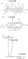
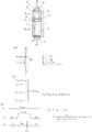
- FIG. 1 is a structural diagram of a dynamic flash memory device according to the first embodiment
- FIG. FIG. 3 is a diagram for explaining an erase operation mechanism of the dynamic flash memory device according to the first embodiment
- FIG. 2 is a diagram for explaining a write operation mechanism of the dynamic flash memory device according to the first embodiment
- FIG. FIG. 2 is a diagram for explaining a read operation mechanism of the dynamic flash memory device according to the first embodiment
- FIG. FIG. 2 is a diagram for explaining a read operation mechanism of the dynamic flash memory device according to the first embodiment
- FIG. 1 is a diagram for explaining a dynamic flash memory cell according to the first embodiment
- FIG. FIG. 4 is a diagram for explaining a dynamic flash memory cell according to a second embodiment
- FIG. 10 is a diagram for explaining a dynamic flash memory cell according to a third embodiment
- FIG. FIG. 12 is a diagram for explaining a dynamic flash memory cell according to a fourth embodiment
- FIG. FIG. 4 is a diagram for explaining operational problems of a conventional DRAM memory cell that does not have a capacitor
- FIG. 4 is a diagram for explaining operational problems of a conventional DRAM memory cell that does not have a capacitor
- FIG. 2 illustrates a read operation of a DRAM memory cell without a conventional capacitor
- dynamic flash memory a memory device using semiconductor elements (hereinafter referred to as dynamic flash memory) according to the present invention will be described with reference to the drawings.
- FIG. 1 The structure and operation mechanism of the dynamic flash memory cell according to the first embodiment of the present invention will be described with reference to FIGS. 1 to 5.
- FIG. 1 The structure of one dynamic flash memory cell will be described with reference to FIG. Then, a data erasing mechanism will be described with reference to FIG. 2, a data writing mechanism will be described with reference to FIG. 3, and a data writing mechanism will be described with reference to FIG.
- FIG. 1 A structure in which four dynamic flash memory cells are formed on the same substrate will be described with reference to FIG.
- FIG. 1 shows the structure of a dynamic flash memory cell according to a first embodiment of the invention.
- Silicon pillars 2 having a conductivity type of P-type or i-type (intrinsic type) are placed on a substrate 1 (which is an example of the “substrate” in the scope of claims) from the bottom (“first semiconductor pillars” in the scope of claims). ) (hereafter, a silicon pillar is referred to as a “Si pillar”), and an N + layer 3a connected to the bottom of the Si pillar 2 (an example of a “first impurity layer” in the scope of claims).
- N + layer 3b which is an example of a “second impurity layer” in the claims
- N + layer 3b which is an example of a “second impurity layer” in the claims
- a channel region 7 is formed between the N + layer 3 a and the N + layer 3 b of the Si pillar 2 .
- a first gate insulating layer 4a surrounding the lower portion of the Si pillar 2 (which is an example of the "first gate insulating layer” in the claims) and a second gate insulating layer 4b surrounding the upper portion of the Si pillar 2. (which is an example of the "second gate insulating layer” in the claims) is formed.
- the first gate insulating layer 4a and the second gate insulating layer 4b are in contact with or close to the N + layers 3a and 3b serving as the source and drain, respectively.
- a first gate conductor layer 5a surrounding the first gate insulating layer 4a (which is an example of the "first gate conductor layer” in the claims) and a second gate insulating layer 4b surrounding the second gate insulating layer 4b.
- a gate conductor layer 5b (which is an example of the "second gate conductor layer” in the claims) is formed respectively.
- the first gate conductor layer 5a and the second gate conductor layer 5b are separated by an insulating layer 6 (which is an example of the "first insulating layer" in the claims).
- the channel region 7 consists of a first channel region 7a surrounded by the first gate insulating layer 4a and a second channel region 7b surrounded by the second gate insulating layer 4b.
- a dynamic flash memory cell 9 is formed from the N + layers 3a and 3b serving as the source and drain, the channel region 7, the first gate insulating layer 4a, the second gate insulating layer 4b, the first gate conductor layer 5a, and the second gate conductor layer 5b.
- a dynamic flash memory cell 9 is formed.
- the N + layer 3a serves as a source line SL (an example of a "source line” in the scope of claims), and the N + layer 3b serves as a bit line BL (an example of a "bit line” in the scope of claims).
- first gate conductor layer 5a is connected to the plate line PL (an example of the "first drive control line” in the claims), and the second gate conductor layer 5b is connected to the word lines WL (claimed , which is an example of a "word line” of the In the memory device, a plurality of dynamic flash memory cells as described above are two-dimensionally arranged on the substrate 1 .
- the substrate 1 is a base material layer connected to the Si pillars 2 standing in the vertical direction and having an upper surface extending in the horizontal direction. Accordingly, the portion of the N + layer 3 a below the surface of the substrate 1 in the vertical direction is referred to as the substrate 1 . The portion of N + layer 3a within this substrate 1 may extend in the horizontal direction. Also, the substrate 1 may be formed of SOI (Silicon On Insulator), single-layered or multi-layered Si, or other semiconductor materials. Further, the substrate 1 may be a well layer composed of a single layer of N layers or P layers, or a plurality of layers.
- SOI Silicon On Insulator
- FIG. 2(a) shows a state in which the hole groups 11 generated by impact ionization in the previous cycle are stored in the channel region 7 before the erasing operation.
- the voltage of the source line SL is set to the negative voltage V ERA during the erasing operation.
- V ERA is, for example, -3V.
- V FB V ERA +Vb.
- the threshold voltage of the second gate conductor layer 5b connected to this word line WL is increased.
- the erased state of this channel region 7 is logical storage data "0".
- the voltage conditions applied to the bit line BL, the source line SL, the word line WL, and the plate line PL are only examples for performing the erase operation, and other operating conditions that enable the erase operation may be used.
- FIG. 3 shows the write operation of the dynamic flash memory cell according to the first embodiment of the invention.
- 0 V for example, is input to the N + layer 3a connected to the source line SL
- 3 V for example, is input to the N + layer 3b connected to the bit line BL
- the plate line PL 2 V for example, is input to the connected first gate conductor layer 5a
- 5 V for example, is input to the second gate conductor layer 5b connected to the word line WL.
- an inversion layer 12a is formed inside the first gate conductor layer 5a to which the plate line PL is connected, and the second gate conductor layer 5a having the first gate conductor layer 5a is formed.
- One N-channel MOS transistor is operated in the linear region.
- a pinch-off point 13 exists in the inversion layer 12a inside the first gate conductor layer 5a to which the plate line PL is connected.
- the second N-channel MOS transistor having the second gate conductor layer 12b connected to the word line WL is operated in the saturation region.
- the inversion layer 12b is formed on the entire surface inside the second gate conductor layer 5b to which the word line WL is connected, without any pinch-off point.
- the inversion layer 12b formed entirely inside the second gate conductor layer 5b connected to the word line WL serves as a substantial drain of the second N-channel MOS transistor having the second gate conductor layer 5b. work.
- the boundary of the channel region 7 between the first N-channel MOS transistor with the series-connected first gate conductor layer 5a and the second N-channel MOS transistor with the second gate conductor layer 5b The electric field is maximized in the region (first boundary region) and the impact ionization phenomenon occurs in this region. Since this region is the region on the source side viewed from the second N-channel MOS transistor having the second gate conductor layer 5b connected to the word line WL, this phenomenon is called the source-side impact ionization phenomenon. Due to this source-side impact ionization phenomenon, electrons flow from the N + layer 3a connected to the source line SL toward the N + layer 3b connected to the bit line.
- Electron-hole pairs can be generated by the impact ionization phenomenon at the boundary between the N + layer 3 a and the channel region 7 or at the boundary between the N + layer 3 b and the channel region 7 .
- the generated hole group 11 is majority carriers in the channel region 7 and charges the channel region 7 with a positive bias. Since the N + layer 3a connected to the source line SL is at 0V, the channel region 7 is at the built-in voltage Vb (approximately 0 V) of the PN junction between the N + layer 3a connected to the source line SL and the channel region 7. .7V).
- Vb approximately 0 V
- the threshold voltages of the first N-channel MOS transistor and the second N-channel MOS transistor are lowered due to the substrate bias effect. Thereby, as shown in FIG. 3(c), the threshold voltage of the N-channel MOS transistor in the second channel region 7b connected to the word line WL is lowered.
- the write state of this channel area 7 is assigned to logical storage data "1".
- Electron-hole pairs may be generated by the impact ionization phenomenon or the GIDL current in the third boundary region, and the channel region 7 may be charged with the generated hole groups 11 .
- the voltage conditions applied to the bit line BL, the source line SL, the word line WL, and the plate line PL are examples for performing the write operation, and other operating conditions that allow the write operation may be used.
- FIGS. 4A and 4B The read operation of the dynamic flash memory cell according to the first embodiment of the present invention and the related memory cell structure will be described with reference to FIGS. 4A and 4B.
- the read operation of the dynamic flash memory cell will be described with reference to FIGS. 4A(a) to 4A(c).
- FIG. 4A(a) when channel region 7 is charged to built-in voltage Vb (approximately 0.7 V), the threshold voltage of the N-channel MOS transistor is lowered due to the substrate bias effect. This state is assigned to logical storage data "1".
- FIG. 4A(b) when the memory block selected before writing is in the erased state "0" in advance, the floating voltage VFB of the channel region 7 is VERA +Vb.
- a write operation randomly stores a write state of "1".
- logical storage data of logical "0" and “1" are created for the word line WL.
- reading is performed by the sense amplifier using the level difference between the two threshold voltages for the word line WL.
- the gate capacitance of the second gate conductor layer 5b connected to the word line WL is preferably designed to be smaller than the gate capacitance of the first gate conductor layer 5a connected to the plate line PL. As shown in FIG. 4B(a), the vertical length of the first gate conductor layer 5a connected to the plate line PL is greater than the vertical length of the second gate conductor layer 5b connected to the word line WL.
- FIG. 4(b) shows an equivalent circuit of one cell of the dynamic flash memory of FIG. 4(a).
- FIG. 4(c) shows the coupling capacity relationship of the dynamic flash memory.
- CWL is the capacitance of the second gate conductor layer 5b
- CPL is the capacitance of the first gate conductor layer 5a
- CBL is the N + layer 3b serving as the drain and the second channel region 7b.
- C SL is the capacitance of the PN junction between the N + layer 3a serving as the source and the first channel region 7a.
- V ReadWL is the amplitude potential at the time of reading the word line WL.
- ⁇ V FB can be reduced by reducing the contribution of C WL compared to the overall capacitance C PL +C WL +C BL +C SL of the channel region 7 .
- C BL +C SL is the capacity of the PN junction, and in order to increase it, for example, the diameter of the Si pillar 2 is increased.
- the vertical length of the first gate conductor layer 5a connected to the plate line PL can be further reduced without lowering the degree of integration of memory cells in plan view.
- the voltage conditions applied to the bit line BL, the source line SL, the word line WL, and the plate line PL are examples for performing the read operation, and other operating conditions that enable the read operation may be used.
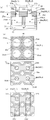
- FIG. 5 shows a structural diagram of a memory device in which four dynamic flash memory cells of this embodiment are formed on a substrate 20.
- FIG. FIG. 5(a) is a vertical sectional view taken along the line X-X' of FIG. 5(b).
- FIG. 5(b) is a horizontal sectional view along line A-A' in FIG. 5(a).
- FIG. 5(c) is a horizontal sectional view along line B-B' in FIG. 5(a).
- FIG. 5(d) is a horizontal sectional view taken along line C-C' in FIG. 5(a). Note that in an actual memory device, more than four dynamic flash memory cells are arranged in rows and columns on the substrate 20.
- FIG. 5(a) is a vertical sectional view taken along the line X-X' of FIG. 5(b).
- FIG. 5(b) is a horizontal sectional view along line A-A' in FIG. 5(a).
- FIG. 5(c) is a horizontal sectional view along line B-
- N + layer 21 which is an example of the “first impurity layer” in the claims
- Si pillars 22a an example of the "first semiconductor pillar” in the claims
- 22b an example of the “second semiconductor pillars” in the claims
- 22c which is an example of the "third semiconductor pillar” in the claims
- 22d which is an example of the "fourth semiconductor pillar” in the claims
- N + layers 29a, 29b, 29c (not shown) and 29d (not shown) are formed on top of the Si pillars 22a to 22d, respectively.
- a SiO 2 layer 24 surrounds the bottoms of the Si pillars 22 a to 22 d and is on the N + layer 21 .
- a HfO 2 layer 25a (which is an example of the "first gate insulating layer” in the claims) surrounds the lower side surfaces of the Si pillars 22a to 22d.
- TiN layer 26a (an example of the "first gate conductor layer” in the scope of claims) surrounding the HfO 2 layer 25a on the side surfaces of the Si pillars 22a and 22b and connected in the XX' line direction. .
- a TiN layer 26b (a " second is an example of the "gate conductor layer of Then, there is an HfO 2 layer 25b (which is an example of the “second gate insulating layer” in the claims) surrounding the upper side surfaces of the Si pillars 22a to 22d and connected to the HfO 2 layer 25a. Then, there is a TiN layer 28a (an example of a "third gate conductor layer” in the scope of claims) surrounding the HfO 2 layer 25b on the side surfaces of the Si pillars 22a and 22b and connected in the XX' line direction. . Similarly, a TiN layer 28b ( a "fourth gate is an example of "conductor layer").
- SiO 2 layer 30 surrounding the TiN layers 26a, 26b, 28a, 28b.
- SiO 2 layer 33 covering the N + layers 29a-29d.
- Contact holes 31a, 31b, 31c and 31d are formed in the SiO 2 layer 33 on the N + layers 29a to 29d.
- a metal wiring layer 32a connected to the N + layers 29a and 29c through contact holes 31a and 31c and extending in a direction perpendicular to the line XX′ and an N + layer through contact holes 31b and 31d.
- metal wiring layer 32b connected to 29b and 29d and extending in a direction perpendicular to line XX'.
- the N + layer 21 is connected to the source line SL explained in FIG. 1
- the TiN layers 26a and 26b are connected to the plate lines PL1 and PL2 which are the plate line PL explained in FIG.
- the metal wiring layers 32a and 32b are connected to the word lines WL1 and WL2 which are the word lines WL described in FIG. 1, and the metal wiring layers 32a and 32b are connected to the bit lines BL1 and BL2 which are described in FIG.
- the TiN layers 26a and 26b surround the HfO 2 layers 25a formed on the side surfaces of the Si pillars 22a to 22d, and are planar. When viewed, it is formed to have a uniform width with a length Lg2 (which is an example of the "second length" in the scope of claims).
- the required film thickness of the TiN layers 26a and 26b is determined from the setting of the threshold voltage required for MOS (Metal Oxide Semiconductor) transistor operation and the required processing margin. As shown in FIG.
- the distance Lg1 between the XX′ line and two points intersecting the outer circumference of the HfO 2 layer 25a surrounding the Si pillars 22a and 22b and facing each other (“ is less than twice Lg2 and equal to or greater than Lg2.
- the distance Lg3 (the , which is an example of a "third length" of Lg2, is greater than twice Lg2.
- the TiN layer 26a connected at the outer periphery of the Si pillars 22a and 22b and the TiN layer 26b connected at the outer periphery of the Si pillars 22c and 22d are formed apart from each other in the XX' direction.
- the TiN layer 26a on the periphery of the Si pillars 22a and 22b on the line XX' becomes a common gate electrode layer for the two dynamic flash memory transistors formed on the Si pillars 22a and 22b.
- the TiN layer 28a connected at the outer periphery of the Si pillars 22a and 22b and the TiN layer 28b connected at the outer periphery of the Si pillars 22c and 22d are formed apart from each other.
- the lengths of the TiN layers 26a and 26b and the TiN layers 28a and 28b may be different as long as the relationship between Lg1, Lg2 and Lg3 is maintained.
- the length Lg2 is the thickness of the TiN layers 26a and 26b in the regions where the gate conductor layers of the Si pillars 22a, 22b, 22c and 22d do not overlap each other.
- the TiN layers 26a and 26b are composed of two layers, for example, a TiN layer that is a gate conductor layer and a TaN layer that is a protective conductor layer (which is an example of the "first conductor layer" in the claims). good too.
- Lg1 can be reduced to the thickness of the TiN layer.
- the TaN layer covering the side surface of the TiN layer serves as a protective film that protects the gate TiN layer during the RIE etching and cleaning processes.
- the TiN layers 26a, 26b may be composed of other conductor single layers consisting of a single layer or multiple layers to serve as gate conductor layers.
- the TiN layers 26a and 26b may be formed from a layer that functions as a gate conductor layer and a layer that functions as a protective film.
- the TiN layers 28a, 28b, including the protective conductor layer may be composed of other conductor single layers consisting of a single layer or multiple layers.
- the plate line PL of the dynamic flash memory cell according to the first embodiment of the present invention changes the voltage of the word line WL during writing and reading operations of the dynamic flash memory cell. to .
- the plate line PL serves to reduce the capacitive coupling ratio between the word line WL and the channel region 7 .
- the influence of the voltage change in the channel region 7 when the voltage of the word line WL swings up and down can be significantly suppressed.
- the threshold voltage difference between the SGT transistors of the word lines WL indicating logic "0" and "1” can be increased. This leads to increased operating margins for dynamic flash memory cells.
- the region of the TiN layer 26a on the line XX' can be a common gate conductor layer for the transistors of the two dynamic flash memory cells formed on the Si pillars 22a and 22b. can.
- the thickness Lg1 of the TiN layer 26a on line XX' can be reduced to Lg2.
- the dynamic flash memory can be highly integrated.
- the diameter of the Si pillars 22a to 22d can be increased, so a large floating body volume can be secured, and many hole groups can be accumulated. As a result, the operating margin can be expanded. (Feature 3)
- the distance Lg3 between the YY′ line perpendicular to the XX′ line and the outer circumference of the facing HfO 2 layer 25a surrounding the Si pillars 22a and 22c is 2 of Lg1. more than doubled.
- the TiN layer 26a connected at the outer peripheral portions of the Si pillars 22a and 22b in the XX′ direction and the TiN layer 26b connected at the outer peripheral portions of the Si pillars 22c and 22d are formed apart from each other.
- Physically separated plate lines PL1 and PL2 are formed.
- the operation mode in which the plate lines PL1 and PL2 are driven independently can be applied to the dynamic flash memory.
- TiN layers 28a and 28b connected to word lines WL1 and WL2 independent of each other can be formed separately.
- FIG. 6 shows a structural diagram of a memory device having four dynamic flash memory cells formed on a substrate 20 according to the second embodiment.
- FIG. 6(a) is a vertical sectional view taken along line XX' of FIG. 6(b).
- FIG. 6(b) is a horizontal sectional view along line AA' of FIG. 6(a).
- FIG. 6(c) is a horizontal sectional view taken along line BB' of FIG. 6(a).
- FIG. 6(d) is a horizontal sectional view taken along line CC' of FIG. 6(a). Note that in an actual memory device, more than four dynamic flash memory cells are arranged in rows and columns.
- First Si pillars 22 aa , 22 ba , 22 ca and 22 da stand on the N + layer 21 .
- Second Si pillars 22ab, 22bb, 22cb and 22db stand on the first Si pillars 22aa, 22ba, 22ca and 22da.
- the outer peripheral lines of the second Si pillars 22ab to 22db are inside the outer peripheral lines of the first Si pillars 22aa to 22da.
- the SiO 2 layer 24, HfO 2 layer 25a, and TiN layers 26a and 26b surrounding the first Si pillars 22aa-22da are constructed in the same manner as the corresponding portions in FIG.
- TiN layer 26a surrounding the HfO 2 layer 25a on the sides of the first Si pillars 22aa, 22ba and connected in the XX' direction.
- TiN layer 26b surrounding the HfO 2 layer 25a on the sides of the first Si pillars 22ca, 22da and connected in a direction parallel to line XX' and separated from the TiN layer 26a.
- HfO 2 layer 25c surrounding the side surfaces of the first Si pillars 22ab to 22db and connected to the HfO 2 layer 25a.
- TiN layer 34a surrounding the HfO 2 layer 25c on the side surfaces of the second Si pillars 22ab and 22bb and connected in the XX' line direction.
- TiN layer 34b surrounding the HfO 2 layer 25c on the side surfaces of the second Si pillars 22cb, 22db, connected in a direction parallel to line XX', and separated from the TiN layer 34a.
- a length LG5 (an example of a “fifth length” in the scope of claims) between two mutually facing points where the YY′ line and the outer peripheral lines of the TiN layers 26a and 26b intersect is the TiN layer It is smaller than the length LG4 between 34a and 34b (which is an example of the "fourth length” in the claims).
- a SiO 2 layer 30 surrounding the TiN layers 26a, 26b, 34a, 34b.
- SiO 2 layer 33 covering the N + layers 35a-35d.
- Contact holes 37a, 37b, 37c and 37d are formed in the SiO 2 layer 33 on the N + layers 35a to 35d.
- a metal wiring layer 32a connected to the N + layers 35a and 35c through contact holes 37a and 37c and extending in a direction perpendicular to the line XX′ and an N + layer through contact holes 37b and 37d.
- the N + layer 21 is connected to the source line SL explained in FIG. 1
- the TiN layers 26a and 26b are connected to the plate lines PL1 and PL2 which are the plate line PL explained in FIG.
- the metal wiring layers 32a and 32b are connected to the bit lines BL1 and BL2, which are the bit lines BL described in FIG.
- This embodiment provides the following features.
- feature 1 the structure of the first Si pillars 22aa to 22da and the surrounding SiO 2 layer 24, HfO 2 layer 25a, and TiN layers 26a and 26b is the same as in FIG.
- the TiN layer 26a connected to the PL1 line on the line XX' serves as a common gate conductor layer of the transistors of the two dynamic flash memory cells formed on the first Si pillar 22aa and the first Si pillar 22ba. can do.
- the thickness Lg1 of the TiN layer 26a on line XX' can be reduced to Lg2.
- the TiN layer 26b connected to the PL2 line on the line parallel to the XX' line is the common gate of the two dynamic flash memory cell transistors formed on the first Si pillar 22ca and the first Si pillar 22da. It becomes a conductor layer and its thickness can be reduced to Lg2. As a result, the dimension of the dynamic flash memory cell in the XX' direction can be reduced, and the integration density of the dynamic flash memory can be increased.
- the outer peripheral lines of the second Si pillars 22ab to 22db in plan view are formed to be inside the outer peripheral lines of the first Si pillars 22aa to 22da.
- the distance Lg4 between the TiN layers 34a and 34b connected to the word lines WL1 and WL2 can be made larger than the distance L5 between the outer peripheral lines of the TiN layers 28a and 28b intersecting the YY' line.
- the capacitance between the word lines WL1 (the capacitance between the TiN layers 34a and 34b) can be made smaller than the capacitance between the word lines WL1 (the capacitance between the TiN layers 28a and 28b) shown in FIG.
- FIG. 7 shows a structural diagram of a memory device having four dynamic flash memory cells formed on a substrate 20 according to the third embodiment.
- FIG. 7(a) is a vertical sectional view taken along line XX' of FIG. 7(b).
- FIG. 7(b) is a horizontal sectional view along line AA' of FIG. 7(a).
- FIG. 7(c) is a horizontal sectional view taken along line BB' of FIG. 7(a).
- FIG. 7(d) is a horizontal sectional view taken along line CC' of FIG. 7(a). Note that in an actual memory device, more than four dynamic flash memory cells are arranged in rows and columns.
- FIG. 7 there is an N + layer 21 on the substrate 20 .
- the first Si pillars 22aa and 22ab standing at the same positions as in FIG. 6 on the N + layer 21 and the first Si pillars 22ca and 22da in FIG.
- first Si pillars 22cA and 22dA standing at moved positions.
- Second Si pillars 22ab, 22bb, 22cB, and 22dB are arranged in order on the first Si pillars 22aa, 22ab, 22cA, and 22dA, respectively.
- the outer peripheral lines of the second Si pillars 22ab to 22dB are inside the outer peripheral lines of the first Si pillars 22aa to 22dA.
- a SiO 2 layer 24 surrounds the bottoms of the first Si pillars 22aa-22dA.
- a HfO 2 layer 25a surrounds the lower side surfaces of the first Si pillars 22aa to 22dA.
- a TiN layer 26A surrounding the HfO 2 layer 25a and connected to the plate line PL connected between the first Si pillars 22aa-22dA.
- there is an HfO 2 layer 25c surrounding the side surfaces of the second Si pillars 22ab-22dB and connected to the HfO 2 layer 25a.
- TiN layer 34a surrounding the HfO 2 layer 25c on the side surfaces of the second Si pillars 22ab, 22bB and connected in the XX' line direction.
- TiN layer 34B surrounding the HfO 2 layer 25c on the side surface of the second Si pillar 22cB, 22dB and connected in a line direction parallel to line XX' and separated from the TiN layer 34a.
- SiO2 layer 30 surrounding the TiN layers 26A, 34a, 34B.
- SiO 2 layer 33 covering the N + layers 35a-35d.
- Contact holes 37a, 37b, 37C and 37D are formed in the SiO 2 layer 33 on the N + layers 35a to 35d.
- a metal wiring layer 32a connected to N + layers 35a and 35c and extending in a direction orthogonal to line XX', and through contact holes 37b and 37D, an N + layer
- a metal wiring layer 32b connected to 35b and 35d and extending in a direction perpendicular to line XX'.
- the TiN layer 26A connected to the plate line PL is formed connecting between the first Si pillars 22aa to 22dA.
- the TiN layers 34a and 34b are connected to the word lines WL1 and WL2, which are the word lines WL described in FIG. 1, and separated from each other.
- the metal wiring layers 32a and 32b are connected to the bit lines BL1 and BL2 which are the bit lines BL described in FIG.
- the thickness Lg2 is the thickness of the TiN layer 26A in a portion that is not in contact with any of the adjacent first Si pillars 22aa to 22dA.
- the distance Lg1 between the line XX′ and two points intersecting the outer circumference of the HfO 2 layer 25a surrounding the first Si pillars 22aa and 22ab and facing each other is shorter than twice Lg2 and equal to Lg2, or big.
- the distance Lg6 between the YY' line and the two points intersecting the outer circumference of the HfO 2 layer 25a surrounding the first Si pillars 22aa and 22cA and facing each other is shorter than twice Lg2 and equal to Lg2. Or big.
- the TiN layer 26A is formed so as to be connected between the first Si pillars 22aa to 22dA.
- the TiN layers 34a and 34B connected to the word lines WL1 and WL2 separated from each other are formed by placing the outer peripheral lines of the second Si pillars 22ab to 22dB inside the first Si pillars 22aa to 22dA. It is formed.
- This embodiment provides the following features.
- the distance between the Si pillars 22aa and 22cA and the distance between the Si pillars 22ab and 22dA could be shortened not only in the XX' line direction but also in the YY' line as compared with FIG. As a result, the integration density of dynamic flash memory cells can be further increased.
- FIG. 8 shows a structural diagram of a memory device having four dynamic flash memory cells formed on a substrate 20 according to the fourth embodiment.
- FIG. 8(a) is a vertical sectional view taken along line XX' of FIG. 8(b).
- FIG. 8(b) is a horizontal sectional view along line AA' of FIG. 8(a).
- FIG. 8(c) is a horizontal sectional view taken along line BB' of FIG. 8(a).
- FIG. 8(d) is a horizontal sectional view taken along line CC' of FIG. 8(a). Note that in an actual memory device, more than four dynamic flash memory cells are arranged in rows and columns.
- the SiO 2 layer 30 was present between the TiN layers 26A.
- a layer 40 is formed.
- the upper surface position of W layer 40 is the same as the upper surface position of TiN layer 26a, and SiO 2 layer 30a is formed between TiN layers 34a and 34B. Others are the same as the third embodiment.
- This embodiment provides the following features.
- the distance between the first Si pillars 22aa and 22cA and between the first Si pillars 22ab and 22dA You can shorten the distance between Further, by providing the W layer 40 between the TiN layers 26A, the dynamic flash memory cell can be highly integrated and the resistance of the plate line PL can be reduced.
- the Si pillar 2 was formed, the semiconductor pillar which consists of semiconductor materials other than this may be used. This also applies to other embodiments according to the present invention.
- the first Si pillars 22aa to 22ad and the second Si pillars 22ab to 22db are formed of the same semiconductor material in FIG. 6, they may be formed of different semiconductor material layers. This also applies to other embodiments according to the present invention.
- the horizontal cross-sectional shape of the Si pillars 22a to 22d in FIG. 5 may be circular, elliptical, or rectangular as long as the relationships of Lg1, Lg2, and Lg3 described in this embodiment can be maintained. This also applies to other embodiments according to the present invention.
- the N + layers 3a and 3b in FIG. 1 may be formed of Si containing donor impurities or other semiconductor material layers. It may also be formed from different semiconductor material layers. Alternatively, the N + layer may be formed by an epitaxial crystal growth method or another method. This also applies to other embodiments according to the present invention.
- TiN layers 26a and 26b are used as gate conductor layers connected to plate lines PL1 and PL2.
- a single layer or a combination of multiple conductive material layers may be used.
- TiN layers 28a and 28b connected to word lines WL1 and WL2 are used.
- a single layer or a combination of multiple conductive material layers may be used.
- the outer sides of the gate TiN layers 16 and 19a may be connected with a wiring metal layer such as W, for example. This also applies to other embodiments according to the present invention.
- the first Si pillars 22aa to 22da and the second Si pillars 22ab to 22db having a rectangular vertical cross section are used for the description, but the vertical cross section may be trapezoidal. Further, the vertical cross sections of the first Si pillars 22aa to 22da and the second Si pillars 22ab to 22db may be rectangular or trapezoidal. These matters are the same in other embodiments according to the present invention.
- the HfO 2 layers 25a and 25b described with reference to FIG. 5 may be other insulating layers consisting of a single layer or multiple layers as long as they function as gate insulating layers. Moreover, each of the HfO 2 layers 25a and 25b may be formed of material layers having different physical values such as material and thickness. This also applies to other embodiments according to the present invention.
- a wiring conductor layer such as a W layer may be formed in order to connect to the N + layer 21 at the bottom of the Si pillars 22a to 22d in FIG. 5 and reduce the resistance of the source line SL. Also, this W layer may be formed every other plurality of Si pillars. This also applies to other embodiments according to the present invention.
- the gate capacitance of the first gate conductor layer 5a connected to the plate line PL is larger than the gate capacitance of the second gate conductor layer 5b connected to the word line WL.
- the gate capacitance of the first gate conductor layer 5a is further reduced to the gate length of the second gate conductor layer 5b. Larger than capacity.
- the film thickness of each gate insulating layer is changed.
- the film thickness of the first gate insulating layer 4a is made thinner than the film thickness of the second gate insulating layer 4b, and the gate capacitance of the first gate conductor layer 5a is reduced to that of the second gate conductor layer 5b.
- the dielectric constant of the material of each gate insulating layer may be changed to make the dielectric constant of the first gate insulating layer 4a higher than that of the second gate insulating layer 4b.
- the gate capacitance of the first gate conductor layer 5a is determined by combining any one of the length of the gate conductor layers 5a and 5b, the film thickness of the gate insulating layers 4a and 4b, and the dielectric constant of the second gate conductor layer 5b. may be even larger than the gate capacitance of . This also applies to other embodiments according to the present invention.
- one of the N + layers 3a and 3b is a P + layer
- the read operation is performed by an operation using a thyristor phenomenon (see, for example, Non-Patent Document 12) or an operation using a tunnel phenomenon.
- a thyristor phenomenon see, for example, Non-Patent Document 12
- an operation using a tunnel phenomenon may This also applies to other embodiments according to the present invention.
- a memory device having semiconductor elements according to the present invention a memory device having high-density and high-performance dynamic flash memory elements can be obtained.
Landscapes
- Engineering & Computer Science (AREA)
- Microelectronics & Electronic Packaging (AREA)
- Computer Hardware Design (AREA)
- Databases & Information Systems (AREA)
- Semiconductor Memories (AREA)
- Non-Volatile Memory (AREA)
Abstract
ソース線SLに繋がるN+層21上に、Si柱22a~22dが立っている。Si柱22a~22dの下部を囲んだHfO2層25aを囲み、且つ分離したプレート線PL1,PL2に繋がるTiN層26a、26bと、Si柱22a~22dの上部を囲んだHfO2層25bを囲むワード線WL1,WL2に繋り、且つ分離したるTiN層28a、28bと、がある。X-X'線上のTiN層26aの厚さLg2が、Y-Y'線上のTiN層26aの厚さLg1の2倍より小さく、且つ1倍と同じか、もしくは大きい。そして、X-X'線上のTiN層28aの厚さLg2が、Y-Y'線上のTiN層28aの厚さLg1の2倍より小さく、且つ1倍と同じか、もしくは大きい。
Description
本発明は、半導体素子を有するメモリ装置に関する。
近年、LSI(Large Scale Integration)技術開発において、半導体素子を有するメモリ装置の高集積化と高性能化が求められている。
通常のプレナー型MOSトランジスタでは、チャネルが半導体基板の上表面に沿う水平方向に延在する。これに対して、SGTのチャネルは、半導体基板の上表面に対して垂直な方向に延在する(例えば、特許文献1、非特許文献1を参照)。このため、SGTはプレナー型MOSトランジスタと比べ、半導体装置の高密度化が可能である。このSGTを選択トランジスタとして用いて、キャパシタを接続したDRAM(Dynamic Random Access Memory、例えば、非特許文献2を参照)、抵抗変化素子を接続したPCM(Phase Change Memory、例えば、非特許文献3を参照)、RRAM(Resistive Random Access Memory、例えば、非特許文献4を参照)、電流により磁気スピンの向きを変化させて抵抗を変化させるMRAM(Magneto-resistive Random Access Memory、例えば、非特許文献5を参照)などの高集積化を行うことができる。また、キャパシタを有しない、1個のMOSトランジスタで構成された、DRAMメモリセル(非特許文献6を参照)などがある。本願は、抵抗変化素子やキャパシタを有しない、MOSトランジスタのみで構成可能な、ダイナミック フラッシュ メモリを有する半導体装置に関する。
図9に、前述したキャパシタを有しない、1個のMOSトランジスタで構成された、DRAMメモリセルの書込み動作を、図10に、動作上の問題点を、図11に、読出し動作を示す(非特許文献6~10を参照)。
図9にDRAMメモリセルの書込み動作を示す。図9(a)は、“1”書込み状態を示している。ここで、メモリセルは、SOI基板101に形成され、ソース線SLが接続されるソースN+層103(以下、ドナー不純物を高濃度で含む半導体領域を「N+層」と称する)、ビット線BLが接続されるドレインN+層104、ワード線WLが接続されるゲート導電層105、MOSトランジスタ110aのフローティングボディ(Floating Body)102により構成され、キャパシタを有さず、MOSトランジスタ110aが1個でDRAMのメモリセルが構成されている。なお、フローティングボディ102直下には、SOI基板のSiO2層101が接している。この1個のMOSトランジスタ110aで構成されたメモリセルの“1”書込みを行う際には、MOSトランジスタ110aを線形領域で動作させる。すなわち、ソースN+層103から延びる電子のチャネル107には、ピンチオフ点108があり、ビット線が接続しているドレインN+層104までには、到達していない。このようにドレインN+層104に接続されたビット線BLとゲート導電層105に接続されたワード線WLを共に高電圧にして、ゲート電圧をドレイン電圧の約1/2程度で、MOSトランジスタ110aを動作させると、ドレインN+層104近傍のピンチオフ点108において、電界強度が最大となる。この結果、ソースN+層103からドレインN+層104に向かって流れる加速された電子は、Siの格子に衝突して、その時に失う運動エネルギーによって、電子・正孔対が生成される(インパクトイオン化現象)。発生した大部分の電子(図示せず)は、ドレインN+層104に到達する。また、ごく一部のとても熱い電子は、ゲート酸化膜109を飛び越えて、ゲート導電層105に到達する。そして、同時に発生した正孔106は、フローティングボディ102を充電する。この場合、発生した正孔は、フローティングボディ102がP型Siのため、多数キャリアの増分として、寄与する。フローティングボディ102は、生成された正孔106で満たされ、フローティングボディ102の電圧がソースN+層103よりもVb以上に高くなると、さらに生成された正孔は、ソースN+層103に放電する。ここで、Vbは、ソースN+層103とP層のフローティングボディ102との間のPN接合のビルトイン電圧であり、約0.7Vである。図9(b)には、生成された正孔106でフローティングボディ102が飽和充電された様子を示している。
次に、図9(c)を用いて、メモリセル110の“0”書込み動作を説明する。共通な選択ワード線WLに対して、ランダムに“1”書込みのメモリセル110aと“0”書込みのメモリセル110bが存在する。図9(c)では、“1”書込み状態から“0”書込み状態に書き換わる様子を示している。“0”書込み時には、ビット線BLの電圧を負バイアスにして、ドレインN+層104とP層のフローティングボディ102との間のPN接合を順バイアスにする。この結果、フローティングボディ102に予め前サイクルで生成された正孔106は、ビット線BLに接続されたドレインN+層104に流れる。書込み動作が終了すると、生成された正孔106で満たされたメモリセル110a(図9(b))と、生成された正孔が吐き出されたメモリセル110b(図9(c))の2つのメモリセルの状態が得られる。正孔106で満たされたメモリセル110aのフローティングボディ102の電位は、生成された正孔がいないフローティングボディ102よりも高くなる。したがって、メモリセル110aのしきい値電圧は、メモリセル110bのしきい値電圧よりも低くなる。その様子を図9(d)に示す。
次に、この1個のMOSトランジスタで構成されたメモリセルの動作上の問題点を、図10を用いて説明する。図10(a)で示したように、フローティングボディ102の容量CFBは、ワード線の接続されたゲートとフローティングボディ102との間の容量CWLと、ソース線の接続されたソースN+層103とフローティングボディ102との間のPN接合の接合容量CSLと、ビット線の接続されたドレインN+層103とフローティングボディ102との間のPN接合の接合容量CBLとの総和で、
CFB = CWL + CBL + CSL (1)
で表される。したがって、書込み時にワード線電圧VWLが振幅すると、メモリセルの記憶ノード(接点)となるフローティングボディ102の電圧も、その影響を受ける。その様子を図10(b)に示している。書込み時にワード線電圧VWLが0VからVProgWLに上昇すると、フローティングボディ102の電圧VFBは、ワード線電圧が変化する前の初期状態の電圧VFB1からVFB2へ、ワード線との容量結合によって上昇する。その電圧変化量ΔVFBは、
ΔVFB = VFB2 - VFB1
= CWL / (CWL + CBL + CSL) × VProgWL (2)
で表される。
ここで、
β= CWL / (CWL + CBL + CSL) (3)
で表され、βをカップリング率と呼ぶ。このようなメモリセルにおいて、CWLの寄与率が大きく、例えば、CWL:CBL:CSL=8:1:1である。この場合、β=0.8となる。ワード線が、例えば、書込み時の5Vから、書込み終了後に0Vになると、ワード線とフローティングボディ102との容量結合によって、フローティングボディ102が、5V×β=4Vも振幅ノイズを受ける。このため、書込み時のフローティングボディ“1”電位と“0”電位との電位差マージンを十分に取れない問題点があった。
CFB = CWL + CBL + CSL (1)
で表される。したがって、書込み時にワード線電圧VWLが振幅すると、メモリセルの記憶ノード(接点)となるフローティングボディ102の電圧も、その影響を受ける。その様子を図10(b)に示している。書込み時にワード線電圧VWLが0VからVProgWLに上昇すると、フローティングボディ102の電圧VFBは、ワード線電圧が変化する前の初期状態の電圧VFB1からVFB2へ、ワード線との容量結合によって上昇する。その電圧変化量ΔVFBは、
ΔVFB = VFB2 - VFB1
= CWL / (CWL + CBL + CSL) × VProgWL (2)
で表される。
ここで、
β= CWL / (CWL + CBL + CSL) (3)
で表され、βをカップリング率と呼ぶ。このようなメモリセルにおいて、CWLの寄与率が大きく、例えば、CWL:CBL:CSL=8:1:1である。この場合、β=0.8となる。ワード線が、例えば、書込み時の5Vから、書込み終了後に0Vになると、ワード線とフローティングボディ102との容量結合によって、フローティングボディ102が、5V×β=4Vも振幅ノイズを受ける。このため、書込み時のフローティングボディ“1”電位と“0”電位との電位差マージンを十分に取れない問題点があった。
図11に読出し動作を示す。図11(a)は、“1”書込み状態を、図11(b)は、“0”書込み状態を示している。しかし、実際には、“1”書込みでフローティングボディ102にVbが書き込まれていても、書込み終了でワード線が0Vに戻ると、フローティングボディ102は、負バイアスに引き下げられる。“0”が書かれる際には、さらに深く負バイアスになってしまうため、書込みの際に“1”と“0”との電位差マージンを十分に大きく出来ない。この動作マージンが小さいことが、本DRAMメモリセルの大きい問題であった。そして、このDRAMメモリセルを駆動するための周辺回路を同一基板上に、如何に形成するかが課題である。
Hiroshi Takato, Kazumasa Sunouchi, Naoko Okabe, Akihiro Nitayama, Katsuhiko Hieda, Fumio Horiguchi, and Fujio Masuoka: IEEE Transaction on Electron Devices, Vol.38, No.3, pp.573-578 (1991)
H. Chung, H. Kim, H. Kim, K. Kim, S. Kim, K. Dong, J. Kim, Y.C. Oh, Y. Hwang, H. Hong, G. Jin, and C. Chung: "4F2 DRAM Cell with Vertical Pillar Transistor(VPT)," 2011 Proceeding of the European Solid-State Device Research Conference, (2011)
H. S. Philip Wong, S. Raoux, S. Kim, Jiale Liang, J. R. Reifenberg, B. Rajendran, M. Asheghi and K. E. Goodson: "Phase Change Memory," Proceeding of IEEE, Vol.98, No 12, December, pp.2201-2227 (2010)
T. Tsunoda, K .Kinoshita, H. Noshiro, Y. Yamazaki, T. Iizuka, Y. Ito, A. Takahashi, A. Okano, Y. Sato, T. Fukano, M. Aoki, and Y. Sugiyama : "Low Power and high Speed Switching of Ti-doped NiO ReRAM under the Unipolar Voltage Source of less than 3V," IEDM (2007)
W. Kang, L. Zhang, J. Klein, Y. Zhang, D. Ravelosona, and W. Zhao: "Reconfigurable Codesign of STT-MRAM Under Process Variations in Deeply Scaled Technology," IEEE Transaction on Electron Devices, pp.1-9 (2015)
M. G. Ertosum, K. Lim, C. Park, J. Oh, P. Kirsch, and K. C. Saraswat : "Novel Capacitorless Single-Transistor Charge-Trap DRAM (1T CT DRAM) Utilizing Electron," IEEE Electron Device Letter, Vol. 31, No.5, pp.405-407 (2010)
J. Wan, L. Rojer, A. Zaslavsky, and S. Critoloveanu: "A Compact Capacitor-Less High-Speed DRAM Using Field Effect-Controlled Charge Regeneration," Electron Device Letters, Vol. 35, No.2, pp.179-181 (2012)
T. Ohsawa, K. Fujita, T. Higashi, Y. Iwata, T. Kajiyama, Y. Asao, and K. Sunouchi: "Memory design using a one-transistor gain cell on SOI," IEEE JSSC, vol.37, No.11, pp1510-1522 (2002).
T. Shino, N. Kusunoki, T. Higashi, T. Ohsawa, K. Fujita, K. Hatsuda, N. Ikumi, F. Matsuoka, Y. Kajitani, R. Fukuda, Y. Watanabe, Y. Minami, A. Sakamoto, J. Nishimura, H. Nakajima, M. Morikado, K. Inoh, T. Hamamoto, A. Nitayama: "Floating Body RAM Technology and its Scalability to 32nm Node and Beyond," IEEE IEDM (2006).
E. Yoshida: "A Capacitorless 1T-DRAM Technology Using Gate-Induced Drain-Leakage (GIDL) Current for Low-Power and High-Speed Embedded Memory," IEEE IEDM (2006).
E. Yoshida, and T. Tanaka: "A Capacitorless 1T-DRAM Technology Using Gate-Induced Drain-Leakage (GIDL) Current for Low-Power and High-Speed Embedded Memory," IEEE Transactions on Electron Devices, Vol. 53, No. 4, pp. 692-697,Apr. 2006.
K.J. Yang, R.N. Gupta, S. Banna, F. Nemati, H.-J. Cho, M. Ershov, M. Tarabbia, D. Hayes, and S.T. Robins, "Optimization of Nanoscale Thyristors on SOI for High-Performance High-Density Memories",2006 IEEE International SOI Conference Proceedings, pp.129-130 (2006)
SGTを用いたメモリ装置でキャパシタを無くした、1個のトランジス型のDRAM(ゲインセル)では、ワード線とフローティングのSGTのボディとの容量結合カップリングが大きく、データ読み出し時や書き込み時にワード線の電位を振幅させると、直接SGTボディへのノイズとして、伝達されてしまう問題点があった。この結果、誤読み出しや記憶データの誤った書き換えの問題を引き起こし、キャパシタを無くした1トランジス型のDRAM(ゲインセル)の実用化が困難となっていた。そして、上記問題を解決すると共に、高密度のメモリ装置を形成する必要がある。
上記の課題を解決するために、本発明に係る柱状半導体素子を用いたメモリ装置は、
基板上に垂直方向に立ち、且つ平面視において第1の線上に中心点を有し、隣接して配置した第1の半導体柱と、第2の半導体柱と、前記第1の線に平行な第2の線上に中心点を有し、隣接して配置した第3の半導体柱と第4の半導体柱と、
前記第1乃至第4の半導体柱の底部に繋がった第1の不純物領域と、
垂直方向において、前記第1の不純物領域の上部にあり、前記第1乃至第4の半導体柱の下方をそれぞれ囲む第1のゲート絶縁層と、
前記第1のゲート絶縁層を囲み、且つ前記第1の半導体柱と前記第2の半導体柱とを囲んで繋がった第1のゲート導体層と、前記第3の半導体柱と前記第4の半導体柱とを囲んで繋がった第2のゲート導体層と、
前記第1のゲート絶縁層の上にあって、前記第1乃至第4の半導体柱の側面を囲む第2のゲート絶縁層と、前記第2のゲート絶縁層を囲み、且つ垂直方向において、上面位置が前記第1乃至第4の半導体柱の頂部下方にあり、且つ前記第1のゲート導体層と、前記第2のゲート導体層と、垂直方向に離れ、且つ前記第1の半導体柱と前記第2の半導体柱とを囲んで繋がった第3のゲート導体層と、
前記第3の半導体柱と前記第4の半導体柱とを囲んで繋がった第4のゲート導体層と、
前記第1乃至第4の半導体柱のそれぞれの頂部に形成された第2の不純物領域と、
前記第1の半導体柱と、前記第3の半導体柱の頂部の前記第2の不純物領域のそれぞれに繋がった第1の配線導体層と、
前記第2の半導体柱と、前記第4の半導体柱の頂部の前記第2の不純物領域のそれぞれに繋がった第2の配線導体層と、を有し、
前記第1及び第2の半導体柱の前記第1のゲート導体層は互いに接触し、前記第2及び第4の半導体柱の前記第1のゲート導体層は互いに接触し、
平面視において、前記第1の半導体柱と、前記第2の半導体柱と、を囲む前記第1のゲート絶縁層の2つの外周線と、前記第1の線との交点の内で向かい合った2点の間の第1の長さが、前記第1のゲート導体層の他と接触していない部分の厚さである第2の長さの2倍より小さく、且つ前記第2の長さの1倍以上であり、
前記第1のゲート導体層と、前記第2のゲート導体層と、前記第3のゲート導体層と、前記第1の不純物領域と、前記第2の不純物領域と、に印加する電圧を制御して、前記第1乃至第4の半導体柱のいずれか、または全ての内部に、インパクトイオン化現象により、またはゲート誘起ドレインリーク電流により生成した正孔群を保持するデータ保持動作と、
前記第1のゲート導体層と、前記第2のゲート導体層と、前記第1の不純物領域と、前記第2の不純物領域と、に印加する電圧を制御して、前記第1乃至4の半導体柱のいずれか、または全ての内部から前記正孔群を除去するデータ消去動作とを行う、
ことを特徴とする(第1発明)。
基板上に垂直方向に立ち、且つ平面視において第1の線上に中心点を有し、隣接して配置した第1の半導体柱と、第2の半導体柱と、前記第1の線に平行な第2の線上に中心点を有し、隣接して配置した第3の半導体柱と第4の半導体柱と、
前記第1乃至第4の半導体柱の底部に繋がった第1の不純物領域と、
垂直方向において、前記第1の不純物領域の上部にあり、前記第1乃至第4の半導体柱の下方をそれぞれ囲む第1のゲート絶縁層と、
前記第1のゲート絶縁層を囲み、且つ前記第1の半導体柱と前記第2の半導体柱とを囲んで繋がった第1のゲート導体層と、前記第3の半導体柱と前記第4の半導体柱とを囲んで繋がった第2のゲート導体層と、
前記第1のゲート絶縁層の上にあって、前記第1乃至第4の半導体柱の側面を囲む第2のゲート絶縁層と、前記第2のゲート絶縁層を囲み、且つ垂直方向において、上面位置が前記第1乃至第4の半導体柱の頂部下方にあり、且つ前記第1のゲート導体層と、前記第2のゲート導体層と、垂直方向に離れ、且つ前記第1の半導体柱と前記第2の半導体柱とを囲んで繋がった第3のゲート導体層と、
前記第3の半導体柱と前記第4の半導体柱とを囲んで繋がった第4のゲート導体層と、
前記第1乃至第4の半導体柱のそれぞれの頂部に形成された第2の不純物領域と、
前記第1の半導体柱と、前記第3の半導体柱の頂部の前記第2の不純物領域のそれぞれに繋がった第1の配線導体層と、
前記第2の半導体柱と、前記第4の半導体柱の頂部の前記第2の不純物領域のそれぞれに繋がった第2の配線導体層と、を有し、
前記第1及び第2の半導体柱の前記第1のゲート導体層は互いに接触し、前記第2及び第4の半導体柱の前記第1のゲート導体層は互いに接触し、
平面視において、前記第1の半導体柱と、前記第2の半導体柱と、を囲む前記第1のゲート絶縁層の2つの外周線と、前記第1の線との交点の内で向かい合った2点の間の第1の長さが、前記第1のゲート導体層の他と接触していない部分の厚さである第2の長さの2倍より小さく、且つ前記第2の長さの1倍以上であり、
前記第1のゲート導体層と、前記第2のゲート導体層と、前記第3のゲート導体層と、前記第1の不純物領域と、前記第2の不純物領域と、に印加する電圧を制御して、前記第1乃至第4の半導体柱のいずれか、または全ての内部に、インパクトイオン化現象により、またはゲート誘起ドレインリーク電流により生成した正孔群を保持するデータ保持動作と、
前記第1のゲート導体層と、前記第2のゲート導体層と、前記第1の不純物領域と、前記第2の不純物領域と、に印加する電圧を制御して、前記第1乃至4の半導体柱のいずれか、または全ての内部から前記正孔群を除去するデータ消去動作とを行う、
ことを特徴とする(第1発明)。
上記の第1発明において、平面視において、前記第1の半導体柱と、前記第3の半導体柱と、を囲む前記第1のゲート絶縁層の2つの外周線と、前記第1の線と直交して、且つ前記第1の半導体柱と前記第3の半導体柱との中心点を通る第3の線と、の交点の内で向かい合った2点の間の第3の長さが、前記第2の長さの2倍より大きいか、又は2倍より小さく、且つ前記第2の長さの1倍以上であることを特徴とする(第2発明)。
上記の第1発明において、平面視において、前記第2のゲート絶縁層に囲まれた部分の前記第1乃至第4の半導体柱の第1の外周線が、前記第1のゲート絶縁層で囲まれた前記第1乃至第4の半導体柱の第2の外周線より内側にあり、
平面視において、前記第1の半導体柱と前記第2の半導体柱とを囲んだ前記第3のゲート導体層と、前記第3の半導体柱と前記第4の半導体柱とを囲んだ前記第4のゲート導体層との間の第4の長さが、前記第1の半導体柱と前記第3の半導体柱とを囲んだ前記第1のゲート導体層と前記第2のゲート導体層との間の第5の長さより大きい、
ことを特徴とする(第3発明)。
平面視において、前記第1の半導体柱と前記第2の半導体柱とを囲んだ前記第3のゲート導体層と、前記第3の半導体柱と前記第4の半導体柱とを囲んだ前記第4のゲート導体層との間の第4の長さが、前記第1の半導体柱と前記第3の半導体柱とを囲んだ前記第1のゲート導体層と前記第2のゲート導体層との間の第5の長さより大きい、
ことを特徴とする(第3発明)。
上記の第1発明において、平面視において、前記第1のゲート導体層の外側を覆って単層または複数層の第1の導体層があることを特徴とする(第4発明)。
上記の第1発明において、前記第1の不純物領域に繋がる配線はソース線であり、前記第2の不純物領域に繋がる配線はビット線であり、前記第1のゲート導体層に繋がる配線は第1の駆動制御線であり、前記第2のゲート導体層と前記第3のゲート導体層第層に繋がる配線はワード線であり、
前記ソース線と、前記ビット線と、前記第1の駆動制御線と、前記ワード線とに印加する電圧により、前記メモリ消去動作と、前記メモリ書き込み動作と、を行う、
ことを特徴とする(第5発明)。
前記ソース線と、前記ビット線と、前記第1の駆動制御線と、前記ワード線とに印加する電圧により、前記メモリ消去動作と、前記メモリ書き込み動作と、を行う、
ことを特徴とする(第5発明)。
上記の第1発明において、前記第1のゲート導体層と、前記第1乃至第4の半導体柱のそれぞれとの間の第1のゲート容量が、前記第2のゲート導体層と、前記第1乃至第4の半導体柱のそれぞれとの間の第2のゲート容量よりも大きいことを特徴とする(第6発明)。
以下、本発明に係る、半導体素子を用いたメモリ装置(以後、ダイナミック フラッシュ メモリと呼ぶ)の実施形態の構造、及び動作について、図面を参照しながら説明する。
(第1実施形態)
図1~図5を用いて、本発明の第1実施形態に係るダイナミック フラッシュ メモリセルの構造と動作メカニズムを説明する。図1を用いて、1個のダイナミック フラッシュ メモリセルの構造を説明する。そして、図2を用いてデータ消去メカニズムを、図3を用いてデータ書き込みメカニズムを、図4を用いてデータ書き込みメカニズムを説明する。図5を用いて、4個のダイナミック フラッシュ メモリセルを、同一基板上に形成した構造を説明する。
図1~図5を用いて、本発明の第1実施形態に係るダイナミック フラッシュ メモリセルの構造と動作メカニズムを説明する。図1を用いて、1個のダイナミック フラッシュ メモリセルの構造を説明する。そして、図2を用いてデータ消去メカニズムを、図3を用いてデータ書き込みメカニズムを、図4を用いてデータ書き込みメカニズムを説明する。図5を用いて、4個のダイナミック フラッシュ メモリセルを、同一基板上に形成した構造を説明する。
図1に、本発明の第1実施形態に係るダイナミック フラッシュ メモリセルの構造を示す。基板1(特許請求の範囲の「基板」の一例である)上に、下からP型又はi型(真性型)の導電型を有するシリコン柱2(特許請求の範囲の「第1の半導体柱」の一例である)(以下、シリコン柱を「Si柱」と称する。)と、Si柱2の底部に繋がるN+層3a(特許請求の範囲の「第1の不純物層」の一例である)と、Si柱2の頂部に繋がるN+層3b(特許請求の範囲の「第2の不純物層」の一例である)とが形成されている。N+層3aとN+層3bは、一方がソースとなる場合に、他方がドレインとなる。そして、Si柱2のN+層3aとN+層3bの間がチャネル領域7となる。このSi柱2の下部を囲む第1のゲート絶縁層4a(特許請求の範囲の「第1のゲート絶縁層」の一例である)と、Si柱2の上部を囲む第2のゲート絶縁層4b(特許請求の範囲の「第2のゲート絶縁層」の一例である)が形成されている。この第1のゲート絶縁層4a、第2のゲート絶縁層4bは、このソース、ドレインとなるN+層3a、3bに、それぞれ接するか、または近接している。この第1のゲート絶縁層4aを囲む第1のゲート導体層5a(特許請求の範囲の「第1のゲート導体層」の一例である)と、第2のゲート絶縁層4bを囲む第2のゲート導体層5b(特許請求の範囲の「第2のゲート導体層」の一例である)がそれぞれ形成されている。そして、第1のゲート導体層5a、第2のゲート導体層5bは絶縁層6(特許請求の範囲の「第1の絶縁層」の一例である)により分離されている。そして、チャネル領域7は、第1のゲート絶縁層4aで囲まれた第1のチャネル領域7aと、第2のゲート絶縁層4bで囲まれた第2のチャネル領域7bと、よりなる。これによりソース、ドレインとなるN+層3a、3b、チャネル領域7、第1のゲート絶縁層4a、第2のゲート絶縁層4b、第1のゲート導体層5a、第2のゲート導体層5bからなるダイナミック フラッシュ メモリセル9が形成される。そして、N+層3aはソース線SL(特許請求の範囲の「ソース線」の一例である)に、N+層3bはビット線BL(特許請求の範囲の「ビット線」の一例である)に、第1のゲート導体層5aはプレート線PL(特許請求の範囲の「第1の駆動制御線」の一例である)に、第2のゲート導体層5bはワード線WL(特許請求の範囲の「ワード線」の一例である)に、それぞれ接続している。メモリ装置では、上述の複数のダイナミック フラッシュ メモリセルが基板1上に2次元状に配置されている。
なお、基板1は垂直方向に立ったSi柱2に繋がり、且つ水平方向の広がった上面を持つ母体材料層である。従って、垂直方向において、N+層3aの内、基板1表面より下方にある部分は基板1とする。この基板1内にあるN+層3aの部分は、水平方向に広がっていてもよい。また、基板1はSOI(Silicon On Insulator)、単層または複数層よりなるSiまたは他の半導体材料より形成してもよい。また、基板1はN層、またはP層の単層、又は複数層よりなるウエル層であってもよい。
図2を用いて、消去動作メカニズムを説明する。N+層3a、3b間のチャネル領域7は、電気的に基板から分離され、フローティングボディとなっている。図2(a)に消去動作前に、前のサイクルでインパクトイオン化により生成された正孔群11がチャネル領域7に蓄えられている状態を示す。そして。図2(b)に示すように、消去動作時には、ソース線SLの電圧を、負電圧VERAにする。ここで、VERAは、例えば、-3Vである。その結果、チャネル領域7の初期電位の値に関係なく、ソース線SLが接続されているソースとなるN+層3aとチャネル領域7のPN接合が順バイアスとなる。その結果、前のサイクルでインパクトイオン化により生成された、チャネル領域7に蓄えられていた、正孔群11が、ソース部のN+層3aに吸い込まれ、チャネル領域7の電位VFBは、VFB=VERA+Vbとなる。ここで、VbはPN接合のビルトイン電圧であり、約0.7Vである。したがって、VERA=-3Vの場合、チャネル領域7の電位は、-2.3Vになる。この値が、消去状態のチャネル領域7の電位状態となる。このため、フローティングボディのチャネル領域7の電位が負の電圧になると、ダイナミック フラッシュ メモリセル9のNチャネルMOSトランジスタのしきい値電圧は、基板バイアス効果によって、高くなる。これにより、図2(c)に示すように、このワード線WLが接続された第2のゲート導体層5bのしきい値電圧は高くなる。このチャネル領域7の消去状態は論理記憶データ“0”となる。なお、上記のビット線BL、ソース線SL、ワード線WL、プレート線PLに印加する電圧条件は、消去動作を行うための一例であり、消去動作ができる他の動作条件であってもよい。
図3に、本発明の第1実施形態に係るダイナミック フラッシュ メモリセルの書込み動作を示す。図3(a)に示すように、ソース線SLの接続されたN+層3aに例えば0Vを入力し、ビット線BLの接続されたN+層3bに例えば3Vを入力し、プレート線PLの接続された第1のゲート導体層5aに、例えば、2Vを入力し、ワード線WLの接続された第2のゲート導体層5bに、例えば、5Vを入力する。その結果、図3(a)に示したように、プレート線PLの接続された第1のゲート導体層5aの内側には、反転層12aが形成され、第1のゲート導体層5aを有する第1のNチャネルMOSトランジスタは線形領域で動作させる。この結果、プレート線PLの接続された第1のゲート導体層5aの内側の反転層12aには、ピンチオフ点13が存在する。一方、ワード線WLの接続された第2のゲート導体層12bを有する第2のNチャネルMOSトランジスタは飽和領域で動作させる。この結果、ワード線WLの接続された第2のゲート導体層5bの内側には、ピンチオフ点は存在せずに全面に反転層12bが形成される。このワード線WLの接続された第2のゲート導体層5bの内側に全面に形成された反転層12bは、第2のゲート導体層5bを有する第2のNチャネルMOSトランジスタの実質的なドレインとして働く。この結果、直列接続された第1のゲート導体層5aを有する第1のNチャネルMOSトランジスタと、第2のゲート導体層5bを有する第2のNチャネルMOSトランジスタとの間のチャネル領域7の境界領域(第1の境界領域)で電界は最大となり、この領域でインパクトイオン化現象が生じる。この領域は、ワード線WLの接続された第2のゲート導体層5bを有する第2のNチャネルMOSトランジスタから見たソース側の領域であるため、この現象をソース側インパクトイオン化現象と呼ぶ。このソース側インパクトイオン化現象により、ソース線SLの接続されたN+層3aからビット線の接続されたN+層3bに向かって電子が流れる。加速された電子が格子Si原子に衝突し、その運動エネルギーによって、電子・正孔対が生成される。生成された電子の一部は、第1のゲート導体層5aと第2のゲート導体層5bに流れるが、大半はビット線BLの接続されたN+層3bに流れる。また、“1”書込みにおいて、ゲート誘起ドレインリーク(GIDL:Gate Induced Drain Leakage)電流を用いて電子・正孔対を発生させ(非特許文献11を参照)、生成された正孔群でフローティングボディFB内を満たしてもよい。なお、インパクトイオン化現象による電子・正孔対の生成は、N+層3aとチャネル領域7の境界、またはN+層3bとチャネル領域7との境界でも行うことが出来る。
そして、図3(b)に示すように、生成された正孔群11は、チャネル領域7の多数キャリアであり、チャネル領域7を正バイアスに充電する。ソース線SLの接続されたN+層3aは、0Vであるため、チャネル領域7はソース線SLの接続されたN+層3aとチャネル領域7との間のPN接合のビルトイン電圧Vb(約0.7V)まで充電される。チャネル領域7が正バイアスに充電されると、第1のNチャネルMOSトランジスタと第2のNチャネルMOSトランジスタのしきい値電圧は、基板バイアス効果によって、低くなる。これにより、図3(c)で示すように、ワード線WLの接続された第2のチャネル領域7bのNチャネルMOSトランジスタのしきい値電圧は、低くなる。このチャネル領域7の書込み状態を論理記憶データ“1”に割り当てる。
なお、書込み動作時に、第1の境界領域に替えて、第1の不純物層と第1のチャネル半導体層との第2の境界領域、または、第2の不純物層と第2のチャネル半導体層との第3の境界領域で、インパクトイオン化現象、またはGIDL電流で、電子・正孔対を発生させ、発生した正孔群11でチャネル領域7を充電しても良い。なお、上記のビット線BL、ソース線SL、ワード線WL、プレート線PLに印加する電圧条件は、書き込み動作を行うための一例であり、書き込み動作ができる他の動作条件であってもよい。
図4A、図4Bを用いて、本発明の第1実施形態に係るダイナミック フラッシュ メモリセルの読出し動作と、これに関係するメモリセル構造を説明する。図4A(a)~図4A(c)を用いて、ダイナミック フラッシュ メモリセルの読出し動作を説明する。図4A(a)に示すように、チャネル領域7がビルトイン電圧Vb(約0.7V)まで充電されると、NチャネルMOSトランジスタのしきい値電圧が基板バイアス効果によって、低下する。この状態を論理記憶データ“1”に割り当てる。図4A(b)に示すように、書込みを行う前に選択するメモリブロックは、予め消去状態“0”にある場合は、チャネル領域7がフローティング電圧VFBはVERA+Vbとなっている。書込み動作によってランダムに書込み状態“1”が記憶される。この結果、ワード線WLに対して、論理“0”と“1”の論理記憶データが作成される。図4A(c)に示すように、このワード線WLに対する2つのしきい値電圧の高低差を利用して、センスアンプで読出しが行われる。
図4B(a)~図4B(d)を用いて、本発明の第1実施形態に係るダイナミック フラッシュ メモリセルの読出し動作時の、2つの第1のゲート導体層5aと第2のゲート導体層5bのゲート容量の大小関係と、これに関係する動作を説明する。ワード線WLの接続する第2のゲート導体層5bのゲート容量は、プレート線PLの接続する第1のゲート導体層5aのゲート容量よりも小さく設計することが望ましい。図4B(a)に示すように、プレート線PLの接続する第1のゲート導体層5aの垂直方向の長さを、ワード線WLの接続する第2のゲート導体層5bの垂直方向の長さより長くして、ワード線WLの接続する第2のゲート導体層5bのゲート容量を、プレート線PLの接続する第1のゲート導体層5aのゲート容量よりも小さくする。図4(b)に図4(a)のダイナミック フラッシュ メモリの1セルの等価回路を示す。そして、図4(c)にダイナミック フラッシュ メモリの結合容量関係を示す。ここで、CWLは第2のゲート導体層5bの容量であり、CPLは第1のゲート導体層5aの容量であり、CBLはドレインとなるN+層3bと第2のチャネル領域7bとの間のPN接合の容量であり、CSLはソースとなるN+層3aと第1のチャネル領域7aとの間のPN接合の容量である。図4(d)に示すように、ワード線WLの電圧が振幅すると、その動作がチャネル領域7にノイズとして影響を与える。この時のチャネル領域7の電位変動ΔVFBは、
ΔVFB = CWL/(CPL+CWL+CBL+CSL) × VReadWL (1)
となる。ここで、VReadWLはワード線WLの読出し時の振幅電位である。式(1)から明らかなようにチャネル領域7の全体の容量CPL+CWL+CBL+CSLに比べて、CWLの寄与率を小さくすれば、ΔVFBは小さくなることが分かる。CBL+CSLはPN接合の容量であり、大きくするためには、例えば、Si柱2の直径を大きくする。しかしメモリセルの微細化に対しては望ましくない。これに対して、プレート線PLの接続する第1のゲート導体層5aの垂直方向の長さを、ワード線WLの接続する第1のゲート導体層5bの垂直方向の長さより更に長くすることによって、平面視におけるメモリセルの集積度を落すことなしに、ΔVFBを更に小さくできる。なお、上記のビット線BL、ソース線SL、ワード線WL、プレート線PLに印加する電圧条件は、読み出し動作を行うための一例であり、読み出し動作ができる他の動作条件であってもよい。
ΔVFB = CWL/(CPL+CWL+CBL+CSL) × VReadWL (1)
となる。ここで、VReadWLはワード線WLの読出し時の振幅電位である。式(1)から明らかなようにチャネル領域7の全体の容量CPL+CWL+CBL+CSLに比べて、CWLの寄与率を小さくすれば、ΔVFBは小さくなることが分かる。CBL+CSLはPN接合の容量であり、大きくするためには、例えば、Si柱2の直径を大きくする。しかしメモリセルの微細化に対しては望ましくない。これに対して、プレート線PLの接続する第1のゲート導体層5aの垂直方向の長さを、ワード線WLの接続する第1のゲート導体層5bの垂直方向の長さより更に長くすることによって、平面視におけるメモリセルの集積度を落すことなしに、ΔVFBを更に小さくできる。なお、上記のビット線BL、ソース線SL、ワード線WL、プレート線PLに印加する電圧条件は、読み出し動作を行うための一例であり、読み出し動作ができる他の動作条件であってもよい。
図5は、本実施形態のダイナミック フラッシュ メモリセルを4個基板20上に形成したメモリ装置の構造図を示す。図5(a)は、図5(b)のX-X’線に沿った垂直断面図である。図5(b)は図5(a)のA-A’線に沿った水平断面図である。図5(c)は図5(a)のB-B’線に沿った水平断面図である。図5(d)は図5(a)のC-C’線に沿った水平断面図である。なお、実際のメモリ装置では、4個よりも多くのダイナミック フラッシュ メモリセルが基板20上に行列状に配置されている。
図5に示すように、基板20上にN+層21(特許請求の範囲の「第1の不純物層」の一例である)がある。そして、N+層21上にSi柱22a(特許請求の範囲の「第1の半導体柱」の一例である)、22b(特許請求の範囲の「第2の半導体柱」の一例である)、22c(特許請求の範囲の「第3の半導体柱」の一例である)、22d(特許請求の範囲の「第4の半導体柱」の一例である)が立っている。そして、Si柱22a~22dの、それぞれの頂部にN+層29a、29b、29c(図示せず)、29d(図示せず)(特許請求の範囲の「第2の不純物層」の一例である)がある。そしてSi柱22a~22dの底部を囲み、且つN+層21上にSiO2層24がある。そして、Si柱22a~22dの下方の側面を囲んでHfO2層25a(特許請求の範囲の「第1のゲート絶縁層」の一例である)がある。そして、Si柱22a、22bの側面のHfO2層25aを囲み且つX-X’線方向に繋がったTiN層26a(特許請求の範囲の「第1のゲート導体層」の一例である)がある。同じく、Si柱22c、22dの側面のHfO2層25aを囲み且つX-X’線に平行な方向に繋がり、且つTiN層26aから分離しているTiN層26b(特許請求の範囲の「第2のゲート導体層」の一例である)がある。そして、Si柱22a~22dの上方の側面を囲み、且つHfO2層25aに繋がったHfO2層25b(特許請求の範囲の「第2のゲート絶縁層」の一例である)がある。そして、Si柱22a、22bの側面のHfO2層25bを囲み且つX-X’線方向に繋がったTiN層28a(特許請求の範囲の「第3のゲート導体層」の一例である)がある。同じく、Si柱22c、22dの側面のHfO2層25bを囲み且つX-X’線に平行な方向に繋がり、且つTiN層28aから分離したTiN層28b(特許請求の範囲の「第4のゲート導体層」の一例である)がある。そして、TiN層26a、26b、28a、28bを囲んでSiO2層30がある。そして、N+層29a~29dを覆ってSiO2層33がある。そして、N+層29a~29d上のSiO2層33にコンタクトホール31a、31b、31c、31dがある。そして、コンタクトホール31a、31cを介して、N+層29a、29cに繋がり、X-X’線と直交した方向に延伸した金属配線層32aと、コンタクトホール31b、31dを介して、N+層29b、29dに繋がり、X-X’線と直交した方向に延伸した金属配線層32bがある。
図5において、N+層21は図1で説明したソース線SLに繋がり、TiN層26a、26bは図1で説明したプレート線PLであるプレート線PL1、PL2に繋がり、TiN層28a、28bは図1で説明したワード線WLであるワード線WL1、WL2に繋がり、金属配線層32a、32bは図1で説明したビット線BLであるBL1、BL2に繋がっている。
図5(b)に示すSi柱22a~22dの各々が十分に離れて形成されている場合、TiN層26a、26bは、Si柱22a~22d側面に形成されたHfO2層25aを囲み、平面視において長さLg2(特許請求の範囲の「第2の長さ」の一例である)で等幅に形成される。TiN層26a、26bの必要な膜厚は、MOS(Metal Oxide Semiconductor)トランジスタ動作上で求められる閾値電圧の設定と、求められる加工マージンの要求から、定められる。図5(b)に示すように、X-X’線と、Si柱22a、22bを囲み、向かい合うHfO2層25aの外周線と交差する2点の間の距離Lg1(特許請求の範囲の「第1の長さ」の一例である)をLg2の2倍より短く、且つLg2と同じか、より大きくする。これにより、そして、X-X’線と直交するY-Y’線とSi柱22a、22cを囲み、向かい合うHfO2層25aの外周線と交差する2点の間の距離Lg3(特許請求の範囲の「第3の長さ」の一例である)をLg2の2倍より大きくする。これにより、X-X’線方向にSi柱22a、22bの外周部で繋がったTiN層26aと、Si柱22c、22dの外周部で繋がったTiN層26bと、が互いに離れて形成される。この場合、X-X’線上にあるSi柱22a、22bの外周部のTiN層26aはSi柱22aとSi柱22bに形成した2つのダイナミック フラッシュ メモリトランジスタに対して共通のゲート電極層となる。そして、図5(c)に示すワード線WLに繋がるTiN層28aとTiN層28bとの関係を、前述のTiN層26aと、TiN層26bと同じにすることにより、X-X’線方向にSi柱22a、22bの外周部で繋がったTiN層28aと、Si柱22c、22dの外周部で繋がったTiN層28bと、が互いに離れて形成される。なお、TiN層26a、26bと、TiN層28a、28bにおいて、各々のLg1、Lg2,Lg3の関係が維持されていれば、それぞれの長さは異なってもよい。また、平面視において、長さLg2はSi柱22aと、22bと、22cと、22dのゲート導体層が互いに重なっていない領域の、TiN層26a、26bの厚さである。
なお、TiN層26a、26bは、例えばゲート導体層であるTiN層と保護導体層であるTaN層(特許請求の範囲の「第1の導体層」の一例である)の2層より構成させてもよい。この場合、MOSトランジスタの閾値電圧をTiN層のみで設定すると、Lg1はTiN層の厚さまで小さくできる。そして、この場合、TaN層は、平面視において、TiN層側面を覆っているTaN層は、RIEエッチング、洗浄プロセスにおいてゲートTiN層を保護する保護膜となる。同様に、TiN層26a、26bは、ゲート導体層となる、単層または複数層よりなる他の導体単層より構成してもよい。また、TiN層26a、26bはゲート導体層としての役割を持つ層と、保護膜としての役割を持つ層より形成してもよい。同様に、TiN層28a、28bも、保護導体層を含めて、単層または複数層よりなる他の導体単層より構成してもよい。
本実施形態は、下記の特徴を供する。
(特徴1)
図1~図4に示したように、本発明の第1実施形態に係るダイナミック フラッシュ メモリセルのプレート線PLはダイナミック フラッシュ メモリセルが書込み、読出し動作をする際に、ワード線WLの電圧が上下に振幅する。この際に、プレート線PLは、ワード線WLとチャネル領域7との間の容量結合比を低減させる役目を担う。この結果、ワード線WLの電圧が上下に振幅する際の、チャネル領域7の電圧変化の影響を著しく抑えることができる。これにより、論理“0”と“1”を示すワード線WLのSGTトランジスタのしきい値電圧差を大きくすることが出来る。これは、ダイナミック フラッシュ メモリセルの動作マージンの拡大に繋がる。
(特徴1)
図1~図4に示したように、本発明の第1実施形態に係るダイナミック フラッシュ メモリセルのプレート線PLはダイナミック フラッシュ メモリセルが書込み、読出し動作をする際に、ワード線WLの電圧が上下に振幅する。この際に、プレート線PLは、ワード線WLとチャネル領域7との間の容量結合比を低減させる役目を担う。この結果、ワード線WLの電圧が上下に振幅する際の、チャネル領域7の電圧変化の影響を著しく抑えることができる。これにより、論理“0”と“1”を示すワード線WLのSGTトランジスタのしきい値電圧差を大きくすることが出来る。これは、ダイナミック フラッシュ メモリセルの動作マージンの拡大に繋がる。
(特徴2)
図5で説明したように、X-X’線上にあるTiN層26aの領域は、Si柱22aとSi柱22bに形成した2つのダイナミック フラッシュ メモリセルのトランジスタの共通のゲート導体層とすることができる。これにより、X-X’線上のTiN層26aの厚さLg1をLg2まで小さくすることができる。これは、ダイナミック フラッシュ メモリセルのX-X’線方向の寸法を小さくできることを示している。このことは、プレート線PL2に繋がるTiN層26b、ワード線WL1、WL2に繋がるTiN層28a、28bに対しても同様である。これにより、ダイナミック フラッシュ メモリの高集積化が図られる。また、同じセル長さであっても、Si柱22a~22dの直径を大きく出来るので、大きいフローティングボディ体積が確保でき、多くの正孔群を溜めることができる。これにより、動作マージンの拡大が図られる。
(特徴3)
図5で説明したように、X-X’線と直交するY-Y’線とSi柱22a、22cを囲み、向かい合うHfO2層25aの外周線で交差する2点間距離Lg3をLg1の2倍より大きくした。これにより、X-X’線方向にSi柱22a、22bの外周部で繋がったTiN層26aと、Si柱22c、22dの外周部で繋がったTiN層26bと、が互いに離れて形成され、電気的に分離したプレート線PL1、PL2が形成される。これにより、プレート線PL1、PL2を独立に駆動する動作モードをダイナミック フラッシュ メモリに適用することができる。同様にして、互いに独立したワード線WL1、WL2に接続した、TiN層28a、28bを離して形成することができる。
図5で説明したように、X-X’線上にあるTiN層26aの領域は、Si柱22aとSi柱22bに形成した2つのダイナミック フラッシュ メモリセルのトランジスタの共通のゲート導体層とすることができる。これにより、X-X’線上のTiN層26aの厚さLg1をLg2まで小さくすることができる。これは、ダイナミック フラッシュ メモリセルのX-X’線方向の寸法を小さくできることを示している。このことは、プレート線PL2に繋がるTiN層26b、ワード線WL1、WL2に繋がるTiN層28a、28bに対しても同様である。これにより、ダイナミック フラッシュ メモリの高集積化が図られる。また、同じセル長さであっても、Si柱22a~22dの直径を大きく出来るので、大きいフローティングボディ体積が確保でき、多くの正孔群を溜めることができる。これにより、動作マージンの拡大が図られる。
(特徴3)
図5で説明したように、X-X’線と直交するY-Y’線とSi柱22a、22cを囲み、向かい合うHfO2層25aの外周線で交差する2点間距離Lg3をLg1の2倍より大きくした。これにより、X-X’線方向にSi柱22a、22bの外周部で繋がったTiN層26aと、Si柱22c、22dの外周部で繋がったTiN層26bと、が互いに離れて形成され、電気的に分離したプレート線PL1、PL2が形成される。これにより、プレート線PL1、PL2を独立に駆動する動作モードをダイナミック フラッシュ メモリに適用することができる。同様にして、互いに独立したワード線WL1、WL2に接続した、TiN層28a、28bを離して形成することができる。
(第2実施形態)
図6は、第2実施形態の4個のダイナミック フラッシュ メモリセルを基板20上に形成したメモリ装置の構造図を示す。図6において、既述の実施形態と同一又は類似の構成部分には同一の符号を付してある。図6(a)は、図6(b)のX-X’線に沿った垂直断面図である。図6(b)は図6(a)のA-A’線に沿った水平断面図である。図6(c)は図6(a)のB-B’線に沿った水平断面図である。図6(d)は図6(a)のC-C’線に沿った水平断面図である。なお、実際のメモリ装置では、4個よりも多くのダイナミック フラッシュ メモリセルが行列状に配置されている。
図6は、第2実施形態の4個のダイナミック フラッシュ メモリセルを基板20上に形成したメモリ装置の構造図を示す。図6において、既述の実施形態と同一又は類似の構成部分には同一の符号を付してある。図6(a)は、図6(b)のX-X’線に沿った垂直断面図である。図6(b)は図6(a)のA-A’線に沿った水平断面図である。図6(c)は図6(a)のB-B’線に沿った水平断面図である。図6(d)は図6(a)のC-C’線に沿った水平断面図である。なお、実際のメモリ装置では、4個よりも多くのダイナミック フラッシュ メモリセルが行列状に配置されている。
図6に示すように、基板20上にN+層21がある。そして、N+層21上に第1のSi柱22aa、22ba、22ca、22daが立っている。そして、第1のSi柱22aa、22ba、22ca、22da上に、第2のSi柱22ab、22bb、22cb、22dbが立っている。平面視において、第2のSi柱22ab~22dbの外周線は、第1のSi柱22aa~22daの外周線より内側にある。第1のSi柱22aa~22daを囲むSiO2層24、HfO2層25a、TiN層26a、26bは、図5の対応する部分と同様に構成されている。第1のSi柱22aa、22baの側面のHfO2層25aを囲み、且つX-X’線方向で繋がったTiN層26aがある。同じく、第1のSi柱22ca、22daの側面のHfO2層25aを囲み且つX-X’線に平行な方向に繋がり、且つTiN層26aから分離したTiN層26bがある。そして、第2のSi柱22ab~22dbの、それぞれの頂部にN+層35a、35b、35c(図示せず)、35d(図示せず)がある。
そして、第1のSi柱22ab~22dbの側面を囲み、且つHfO2層25aに繋がったHfO2層25cがある。そして、第2のSi柱22ab、22bbの側面のHfO2層25cを囲み且つX-X’線方向に繋がったTiN層34aがある。同じく、第2のSi柱22cb、22dbの側面のHfO2層25cを囲み且つX-X’線に平行な方向に繋がり、且つTiN層34aと分離したTiN層34bがある。Y-Y’線とTiN層26a、26bの外周線とが交わる、互いに向き合う2点の間の長さLG5(特許請求の範囲の「第5の長さ」の一例である)は、TiN層34a、34bの間の長さLG4(特許請求の範囲の「第4の長さ」の一例である)より小さくなる。そして、TiN層26a、26b、34a、34bを囲んでSiO2層30がある。そして、N+層35a~35dを覆ってSiO2層33がある。そして、N+層35a~35d上のSiO2層33にコンタクトホール37a、37b、37c、37dがある。そして、コンタクトホール37a、37cを介して、N+層35a、35cに繋がり、X-X’線と直交した方向に延伸した金属配線層32aと、コンタクトホール37b、37dを介して、N+層35b、35dとに繋がり、X-X’線と直交した方向に延伸した金属配線層32bがある。
図6において、N+層21は図1で説明したソース線SLに繋がり、TiN層26a、26bは図1で説明したプレート線PLであるプレート線PL1、PL2に繋がり、TiN層34a、34bは図1で説明したワード線WLであるワード線WL1、WL2に繋がり、金属配線層32a、32bは図1で説明したビット線BLであるビット線BL1、BL2に繋がっている。
図6(c)に示すように、第2のSi柱22ab、22bb、22cb、22dbの直径が、第1のSi柱22aa、22ba、22ca、22daの直径より小さくなっているので、ワード線WL1、WL2に繋がるTiN層34a、34bの間の距離Lg4は、図5(c)に示したTiN層28a、28bの間の距離(=Lg3―2Lg2)より大きくなる。
本実施形態は、下記の特徴を供する。
(特徴1)
本実施形態では、第1のSi柱22aa~22daと、それらを囲むSiO2層24、HfO2層25a、TiN層26a、26bによる構造は、図5と同じである。これにより、X-X’線上にあるPL1線に繋がるTiN層26aは、第1のSi柱22aaと第1のSi柱22baに形成した2つのダイナミック フラッシュ メモリセルのトランジスタの共通のゲート導体層とすることができる。これにより、X-X’線上のTiN層26aの厚さLg1をLg2まで小さくすることができる。同じく、X-X’線に平行な線上にあるPL2線に繋がるTiN層26bは、第1のSi柱22caと第1のSi柱22daに形成した2つのダイナミック フラッシュ メモリセルのトランジスタの共通のゲート導体層となり、その厚さはLg2まで小さくすることができる。これにより、ダイナミック フラッシュ メモリセルのX-X’線方向の寸法を小さくでき、ダイナミック フラッシュ メモリの高集積化が図られる。
(特徴1)
本実施形態では、第1のSi柱22aa~22daと、それらを囲むSiO2層24、HfO2層25a、TiN層26a、26bによる構造は、図5と同じである。これにより、X-X’線上にあるPL1線に繋がるTiN層26aは、第1のSi柱22aaと第1のSi柱22baに形成した2つのダイナミック フラッシュ メモリセルのトランジスタの共通のゲート導体層とすることができる。これにより、X-X’線上のTiN層26aの厚さLg1をLg2まで小さくすることができる。同じく、X-X’線に平行な線上にあるPL2線に繋がるTiN層26bは、第1のSi柱22caと第1のSi柱22daに形成した2つのダイナミック フラッシュ メモリセルのトランジスタの共通のゲート導体層となり、その厚さはLg2まで小さくすることができる。これにより、ダイナミック フラッシュ メモリセルのX-X’線方向の寸法を小さくでき、ダイナミック フラッシュ メモリの高集積化が図られる。
(特徴2)
本実施形態では、平面視における第2のSi柱22ab~22dbの外周線を、第1のSi柱22aa~22daの外周線より内側になるように形成した。これにより、ワード線WL1、WL2に繋がるTiN層34a、34bの間の距離Lg4は、Y-Y’線と交わるTiN層28a、28bの外周線の間の距離L5より大きくできる。これにより、ワード線WL1間容量(TiN層34a、34b間容量)を、図5で示したワード線WL1間容量(TiN層28a、28b間容量)より小さくできる。また、TiN層34a、34bの間の距離を大きくできることにより、TiN層34a、34b間に更にワード線WL1、WL2間容量を小さくするための、例えば空孔(エアギャップ)の形成が容易になる。これによりダイナミック フラッシュ メモリの動作マージンの拡大が図られる。
本実施形態では、平面視における第2のSi柱22ab~22dbの外周線を、第1のSi柱22aa~22daの外周線より内側になるように形成した。これにより、ワード線WL1、WL2に繋がるTiN層34a、34bの間の距離Lg4は、Y-Y’線と交わるTiN層28a、28bの外周線の間の距離L5より大きくできる。これにより、ワード線WL1間容量(TiN層34a、34b間容量)を、図5で示したワード線WL1間容量(TiN層28a、28b間容量)より小さくできる。また、TiN層34a、34bの間の距離を大きくできることにより、TiN層34a、34b間に更にワード線WL1、WL2間容量を小さくするための、例えば空孔(エアギャップ)の形成が容易になる。これによりダイナミック フラッシュ メモリの動作マージンの拡大が図られる。
(第3実施形態)
図7は、第3実施形態の4個のダイナミック フラッシュ メモリセルを基板20上に形成したメモリ装置の構造図を示す。図7において、既述の実施形態と同一又は類似の構成部分には同一の符号を付してある。図7(a)は、図7(b)のX-X’線に沿った垂直断面図である。図7(b)は図7(a)のA-A’線に沿った水平断面図である。図7(c)は図7(a)のB-B’線に沿った水平断面図である。図7(d)は図7(a)のC-C’線に沿った水平断面図である。なお、実際のメモリ装置では、4個よりも多くのダイナミック フラッシュ メモリセルが行列状に配置されている。
図7は、第3実施形態の4個のダイナミック フラッシュ メモリセルを基板20上に形成したメモリ装置の構造図を示す。図7において、既述の実施形態と同一又は類似の構成部分には同一の符号を付してある。図7(a)は、図7(b)のX-X’線に沿った垂直断面図である。図7(b)は図7(a)のA-A’線に沿った水平断面図である。図7(c)は図7(a)のB-B’線に沿った水平断面図である。図7(d)は図7(a)のC-C’線に沿った水平断面図である。なお、実際のメモリ装置では、4個よりも多くのダイナミック フラッシュ メモリセルが行列状に配置されている。
図7に示すように、基板20上にN+層21がある。そして、N+層21上に、図6と同じ位置に立つ第1のSi柱22aa、22abと、図6の第1のSi柱22ca、22daが、Y-Y’線に沿って上方に平行移動した位置に立つ第1のSi柱Si柱22cA、22dAがある。そして、第1のSi柱22aa、22ab、22cA、22dAそれぞれの上に、順に第2のSi柱22ab、22bb、22cB、22dBがある。平面視において、第2のSi柱22ab~22dBの外周線は、第1のSi柱22aa~22dAの外周線より内側にある。第1のSi柱22aa~22dAの底部を囲んでSiO2層24がある。そして、第1のSi柱22aa~22dAの下部の側面を囲んでHfO2層25aがある。そして、HfO2層25aを囲み、且つ第1のSi柱22aa~22dA間で繋がったプレート線PLに繋がるTiN層26Aがある。そして、第2のSi柱22ab~22dBの、それぞれの頂部にN+層35a、35b、35c(図示せず)、35d(図示せず)がある。そして、第2のSi柱22ab~22dBの側面を囲み、且つHfO2層25aに繋がったHfO2層25cがある。そして、第2のSi柱22ab、22bBの側面のHfO2層25cを囲み且つX-X’線方向に繋がったTiN層34aがある。同じく、第2のSi柱22cB、22dBの側面のHfO2層25cを囲み且つX-X’線と並行した線方向に繋がり、且つTiN層34aと分離したTiN層34Bがある。そして、TiN層26A、34a、34Bを囲んでSiO2層30がある。そして、N+層35a~35dを覆ってSiO2層33がある。そして、N+層35a~35d上のSiO2層33にコンタクトホール37a、37b、37C、37Dがある。そして、コンタクトホール37a、37Cを介して、N+層35a、35cに繋がり、X-X’線と直交した方向に延伸した金属配線層32aと、コンタクトホール37b、37Dを介して、N+層35b、35dとに繋がり、X-X’線と直交した方向に延伸した金属配線層32bがある。
図7において、プレート線PLと繋がるTiN層26Aは、第1のSi柱22aa~22dA間に繋がって形成される。TiN層34a、34bは図1で説明したワード線WLであるワード線WL1、WL2に繋がって、互いに分離して形成される。そして、金属配線層32a、32bは図1で説明したビット線BLであるビット線BL1,BL2に繋がっている。
図7において、平面視において、厚さLg2は、隣接する第1のSi柱22aa~22dAのいずれとも接していない部分のTiN層26Aの厚さである。X-X’線と、第1のSi柱22aa、22abを囲み、向かい合うHfO2層25aの外周線と交差する2点の間の距離Lg1がLg2の2倍より短く、且つLg2と同じか、大きい。同じく、Y-Y’線と、第1のSi柱22aa、22cAを囲み、向かい合うHfO2層25aの外周線で交差する2点の間の距離Lg6がLg2の2倍より短く、且つLg2と同じか、大きい。これにより、TiN層26Aは第1のSi柱22aa~22dA間で繋がって形成される。そして、平面視において、第2のSi柱22ab~22dBの外周線を第1のSi柱22aa~22dAより内側にすることにより、互いに分離したワード線WL1,WL2に接続するTiN層34a、34Bが形成される。
本実施形態は、下記の特徴を供する。
本実施形態では、図6と比べて、X-X’線方向だけでなく、Y-Y’線においても、Si柱22aa、22cA間、及びSi柱22ab、22dA間の距離を短くできた。これにより、更にダイナミック フラッシュ メモリセルの高集積化が図られる。
本実施形態では、図6と比べて、X-X’線方向だけでなく、Y-Y’線においても、Si柱22aa、22cA間、及びSi柱22ab、22dA間の距離を短くできた。これにより、更にダイナミック フラッシュ メモリセルの高集積化が図られる。
(第4実施形態)
図8は、第4実施形態の4個のダイナミック フラッシュ メモリセルを基板20上に形成したメモリ装置の構造図を示す。図8において、既述の実施形態と同一又は類似の構成部分には同一の符号を付してある。図8(a)は、図8(b)のX-X’線に沿った垂直断面図である。図8(b)は図8(a)のA-A’線に沿った水平断面図である。図8(c)は図8(a)のB-B’線に沿った水平断面図である。図8(d)は図8(a)のC-C’線に沿った水平断面図である。なお、実際のメモリ装置では、4個よりも多くのダイナミック フラッシュ メモリセルが行列状に配置されている。
図8は、第4実施形態の4個のダイナミック フラッシュ メモリセルを基板20上に形成したメモリ装置の構造図を示す。図8において、既述の実施形態と同一又は類似の構成部分には同一の符号を付してある。図8(a)は、図8(b)のX-X’線に沿った垂直断面図である。図8(b)は図8(a)のA-A’線に沿った水平断面図である。図8(c)は図8(a)のB-B’線に沿った水平断面図である。図8(d)は図8(a)のC-C’線に沿った水平断面図である。なお、実際のメモリ装置では、4個よりも多くのダイナミック フラッシュ メモリセルが行列状に配置されている。
平面視において、図7においては、TiN層26Aの間にSiO2層30があったのに対して、図8(b)に示すように、SiO2層30に替えて、例えばタングステン(W)層40が形成される。W層40の上面位置はTiN層26aの上面位置と同じである、そして、TiN層34a、34B間にはSiO2層30aが形成される。他は、第3実施形態と同じである。
本実施形態は、下記の特徴を供する。
本実施形態では、第3実施形態と同じく、X-X’線方向だけでなく、Y-Y’線方向においても、第1のSi柱22aa、22cA間、及び第1のSi柱22ab、22dA間の距離を短くできる。更にTiN層26A間にW層40を設けることにより、ダイナミック フラッシュ メモリセルの高集積化が図られると共に、プレート線PLの低抵抗化が図られる。
本実施形態では、第3実施形態と同じく、X-X’線方向だけでなく、Y-Y’線方向においても、第1のSi柱22aa、22cA間、及び第1のSi柱22ab、22dA間の距離を短くできる。更にTiN層26A間にW層40を設けることにより、ダイナミック フラッシュ メモリセルの高集積化が図られると共に、プレート線PLの低抵抗化が図られる。
(その他の実施形態)
なお、第1実施形態の図1では、Si柱2を形成したが、これ以外の半導体材料よりなる半導体柱であってもよい。このことは、本発明に係るその他の実施形態においても同様である。また、図6では第1のSi柱22aa~22adと第2のSi柱22ab~22dbとを同じ半導体材料で形成したが、異なる半導体材料層により形成してもよい。このことは、本発明に係るその他の実施形態においても同様である。
なお、第1実施形態の図1では、Si柱2を形成したが、これ以外の半導体材料よりなる半導体柱であってもよい。このことは、本発明に係るその他の実施形態においても同様である。また、図6では第1のSi柱22aa~22adと第2のSi柱22ab~22dbとを同じ半導体材料で形成したが、異なる半導体材料層により形成してもよい。このことは、本発明に係るその他の実施形態においても同様である。
なお、図5におけるSi柱22a~22dの水平断面形状は、本実施形態で説明したLg1,Lg2,Lg3の関係が維持できるならば、円形状、楕円状、長方形状であってもよい。このことは、本発明に係るその他の実施形態においても同様である。
また、図1における、N+層3a、3bは、ドナー不純物を含んだSi、または他の半導体材料層より形成されてもよい。また、異なる半導体材料層より形成されてもよい。また、それらの形成方法はエピタキシャル結晶成長法、または、他の方法でN+層を形成してもよい。このことは、本発明に係るその他の実施形態においても同様である。
また、図5では、プレート線PL1,PL2に繋がるゲート導体層としてTiN層26a、26bを用いた。これに対して、TiN層26a、26bに替えて、単層または複数の導体材料層を組み合わせて用いてもよい。同じく、ワード線WL1,WL2に繋がった、TiN層28a、28bを用いた。これに対して、TiN層28a、28bに替えて、単層または複数の導体材料層を組み合わせて用いてもよい。また、ゲートTiN層16、19aの外側を、例えばWなどの配線金属層で繋げてもよい。このことは、本発明に係るその他の実施形態においても同様である。
また、図6では、矩形状の垂直断面を有する第1のSi柱22aa~22da、第2のSi柱22ab~22dbを用いて説明したが、これら垂直断面形状は台形状であってもよい。また、第1のSi柱22aa~22da、第2のSi柱22ab~22dbの垂直断面のそれぞれが矩形状、台形状に異なっていてもよい。これらのことは、本発明に係るその他の実施形態においても同様である。
なお、図5で説明した、HfO2層25a、25bは、ゲート絶縁層として機能するものであれば、単層、又は複数層よりなる他の絶縁層であってもよい。また、HfO2層25a、25bのそれぞれは、材料、厚さなどの物理的値が異なる材料層より形成してもよい。このことは、本発明に係るその他の実施形態においても同様である。
また、図5における、Si柱22a~22dの底部のN+層21に接続して、ソース線SL抵抗を下げるために、例えばW層などの配線導体層を形成してもよい。また、このW層を複数のSi柱おきに形成してもよい。このことは、本発明に係るその他の実施形態においても同様である。
また、図1において、プレート線PLに接続された第1のゲート導体層5aのゲート容量が、ワード線WLに接続された第2のゲート導体層5bのゲート容量よりも大きくなるように、第1のゲート導体層5aのゲート長を、第2のゲート導体層5bのゲート長よりも長くすることにより、更に第1のゲート導体層5aのゲート容量を、第2のゲート導体層5bのゲート容量よりも、大きく出来る。また、その他にも、第1のゲート導体層5aのゲート長を、第2のゲート導体層5bのゲート長よりも長くする、または長くしない構造においても、それぞれのゲート絶縁層の膜厚を変えて、第1のゲート絶縁層4aの膜厚を、第2のゲート絶縁層4bの膜厚よりも薄くして、更に第1のゲート導体層5aのゲート容量を、第2のゲート導体層5bのゲート容量よりも、大きく出来る。また、それぞれのゲート絶縁層の材料の誘電率を変えて、第1のゲート絶縁層4aの誘電率を、第2のゲート絶縁層4bの誘電率よりも高くしてもよい。また、ゲート導体層5a、5bの長さ、ゲート絶縁層4a、4bの膜厚、誘電率のいずれかを組み合わせて、第1のゲート導体層5aのゲート容量が、第2のゲート導体層5bのゲート容量よりも、更に大きくしてもよい。このことは、本発明に係るその他の実施形態においても同様である。
また、図1において、N+層3a、3bの一方をP+層にして読み出し動作を、サイリスタ現象を用いた動作(例えば、非特許文献12を参照)、またはトンネル現象を用いた動作により行ってもよい。このことは、本発明に係るその他の実施形態においても同様である。
また、本発明は、本発明の広義の精神と範囲を逸脱することなく、様々な実施形態及び変形が可能とされるものである。また、上述した各実施形態は、本発明の一実施例を説明するためのものであり、本発明の範囲を限定するものではない。上記実施例及び変形例は任意に組み合わせることができる。さらに、必要に応じて上記実施形態の構成要件の一部を除いても本発明の技術思想の範囲内となる。
本発明に係る、半導体素子を有するメモリ装置によれば、高密度で、かつ高性能のダイナミック フラッシュ メモリ素子を有するメモリ装置が得られる。
1、20: 基板
2、22a、22b、22c、22d: Si柱
22aa、22ba、22ca、22da、22cA、22dA: 第1のSi柱
22ab、22bb、22cb、22db: 第2のSi柱
3a、3b、21、29a、29b、29c、29d、35a、35b、35c、35d: N+層
4a: 第1のゲート絶縁層
4b: 第2のゲート絶縁層
5a: 第1のゲート導体層
5b: 第2のゲート導体層
6: 絶縁層
7: チャネル領域
7a: 第1のチャネル層
7b: 第2のチャネル層
SL: ソース線
PL、PL1,PL2: プレート線
WL、WL1,WL2: ワード線
BL、BL1,BL2: ビット線
11: 正孔群
12a、12b: 反転層
25a、25b、25c: HfO2層
26a、26b、26A,28a、28b、34a、34b、34B: TiN層
24、30,33: SiO2層
32a、32b: 金属配線層
31a、31b、32c、32d、37a、37b、37c、37d: コンタクトホール
40: W層
2、22a、22b、22c、22d: Si柱
22aa、22ba、22ca、22da、22cA、22dA: 第1のSi柱
22ab、22bb、22cb、22db: 第2のSi柱
3a、3b、21、29a、29b、29c、29d、35a、35b、35c、35d: N+層
4a: 第1のゲート絶縁層
4b: 第2のゲート絶縁層
5a: 第1のゲート導体層
5b: 第2のゲート導体層
6: 絶縁層
7: チャネル領域
7a: 第1のチャネル層
7b: 第2のチャネル層
SL: ソース線
PL、PL1,PL2: プレート線
WL、WL1,WL2: ワード線
BL、BL1,BL2: ビット線
11: 正孔群
12a、12b: 反転層
25a、25b、25c: HfO2層
26a、26b、26A,28a、28b、34a、34b、34B: TiN層
24、30,33: SiO2層
32a、32b: 金属配線層
31a、31b、32c、32d、37a、37b、37c、37d: コンタクトホール
40: W層
Claims (6)
- 基板上に垂直方向に立ち、且つ平面視において第1の線上に中心点を有し、隣接して配置した第1の半導体柱と、第2の半導体柱と、前記第1の線に平行な第2の線上に中心点を有し、隣接して配置した第3の半導体柱と第4の半導体柱と、
前記第1乃至第4の半導体柱の底部に繋がった第1の不純物領域と、
垂直方向において、前記第1の不純物領域の上部にあり、前記第1乃至第4の半導体柱の下方をそれぞれ囲む第1のゲート絶縁層と、
前記第1のゲート絶縁層を囲み、且つ前記第1の半導体柱と前記第2の半導体柱とを囲んで繋がった第1のゲート導体層と、前記第3の半導体柱と前記第4の半導体柱とを囲んで繋がった第2のゲート導体層と、
前記第1のゲート絶縁層の上にあって、前記第1乃至第4の半導体柱の側面を囲む第2のゲート絶縁層と、前記第2のゲート絶縁層を囲み、且つ垂直方向において、上面位置が前記第1乃至第4の半導体柱の頂部下方にあり、且つ前記第1のゲート導体層と、前記第2のゲート導体層と、垂直方向に離れ、且つ前記第1の半導体柱と前記第2の半導体柱とを囲んで繋がった第3のゲート導体層と、
前記第3の半導体柱と前記第4の半導体柱とを囲んで繋がった第4のゲート導体層と、
前記第1乃至第4の半導体柱のそれぞれの頂部に形成された第2の不純物領域と、
前記第1の半導体柱と、前記第3の半導体柱の頂部の前記第2の不純物領域のそれぞれに繋がった第1の配線導体層と、
前記第2の半導体柱と、前記第4の半導体柱の頂部の前記第2の不純物領域のそれぞれに繋がった第2の配線導体層と、を有し、
前記第1及び第2の半導体柱の前記第1のゲート導体層は互いに接触し、前記第2及び第4の半導体柱の前記第1のゲート導体層は互いに接触し、
平面視において、前記第1の半導体柱と、前記第2の半導体柱と、を囲む前記第1のゲート絶縁層の2つの外周線と、前記第1の線との交点の内で向かい合った2点の間の第1の長さが、前記第1のゲート導体層の他と接触していない部分の厚さである第2の長さの2倍より小さく、且つ前記第2の長さの1倍以上であり、
前記第1のゲート導体層と、前記第2のゲート導体層と、前記第3のゲート導体層と、前記第1の不純物領域と、前記第2の不純物領域と、に印加する電圧を制御して、前記第1乃至第4の半導体柱のいずれか、または全ての内部に、インパクトイオン化現象により、またはゲート誘起ドレインリーク電流により生成した正孔群を保持するデータ保持動作と、
前記第1のゲート導体層と、前記第2のゲート導体層と、前記第1の不純物領域と、前記第2の不純物領域と、に印加する電圧を制御して、前記第1乃至4の半導体柱のいずれか、または全ての内部から前記正孔群を除去するデータ消去動作とを行う、
ことを特徴とする柱状半導体素子を用いたメモリ装置。 - 平面視において、前記第1の半導体柱と、前記第3の半導体柱と、を囲む前記第1のゲート絶縁層の2つの外周線と、前記第1の線と直交して、且つ前記第1の半導体柱と前記第3の半導体柱との中心点を通る第3の線と、の交点の内で向かい合った2点の間の第3の長さが、前記第2の長さの2倍より大きいか、又は2倍より小さく、且つ前記第2の長さの1倍以上である、
ことを特徴とする請求項1に記載の柱状半導体素子を用いたメモリ装置。 - 平面視において、前記第2のゲート絶縁層に囲まれた部分の前記第1乃至第4の半導体柱の第1の外周線が、前記第1のゲート絶縁層で囲まれた前記第1乃至第4の半導体柱の第2の外周線より内側にあり、
平面視において、前記第1の半導体柱と前記第2の半導体柱とを囲んだ前記第3のゲート導体層と、前記第3の半導体柱と前記第4の半導体柱とを囲んだ前記第4のゲート導体層との間の第4の長さが、前記第1の半導体柱と前記第3の半導体柱とを囲んだ前記第1のゲート導体層と前記第2のゲート導体層との間の第5の長さより大きい、
ことを特徴とする請求項1に記載の柱状半導体素子を用いたメモリ装置。 - 平面視において、前記第1のゲート導体層の外側を覆って単層または複数層の第1の導体層がある、
ことを特徴とする請求項1に記載の柱状半導体素子を用いたメモリ装置。 - 前記第1の不純物領域に繋がる配線はソース線であり、前記第2の不純物領域に繋がる配線はビット線であり、前記第1のゲート導体層に繋がる配線は第1の駆動制御線であり、前記第2のゲート導体層と前記第3のゲート導体層第層に繋がる配線はワード線であり、
前記ソース線と、前記ビット線と、前記第1の駆動制御線と、前記ワード線とに印加する電圧により、前記メモリ消去動作と、前記メモリ書き込み動作と、を行う、
ことを特徴とする請求項1に記載の柱状半導体素子を用いたメモリ装置。 - 前記第1のゲート導体層と、前記第1乃至第4の半導体柱のそれぞれとの間の第1のゲート容量が、前記第2のゲート導体層と、前記第1乃至第4の半導体柱のそれぞれとの間の第2のゲート容量よりも大きい、
ことを特徴とする請求項1に記載の柱状半導体素子を用いたメモリ装置。
Priority Applications (3)
| Application Number | Priority Date | Filing Date | Title |
|---|---|---|---|
| PCT/JP2021/017504 WO2022234656A1 (ja) | 2021-05-07 | 2021-05-07 | 半導体素子を有するメモリ装置 |
| TW111110593A TWI806509B (zh) | 2021-05-07 | 2022-03-22 | 使用柱狀半導體元件的記憶裝置 |
| US17/735,414 US11925013B2 (en) | 2021-05-07 | 2022-05-03 | Memory device using pillar-shaped semiconductor element |
Applications Claiming Priority (1)
| Application Number | Priority Date | Filing Date | Title |
|---|---|---|---|
| PCT/JP2021/017504 WO2022234656A1 (ja) | 2021-05-07 | 2021-05-07 | 半導体素子を有するメモリ装置 |
Publications (1)
| Publication Number | Publication Date |
|---|---|
| WO2022234656A1 true WO2022234656A1 (ja) | 2022-11-10 |
Family
ID=83900638
Family Applications (1)
| Application Number | Title | Priority Date | Filing Date |
|---|---|---|---|
| PCT/JP2021/017504 Ceased WO2022234656A1 (ja) | 2021-05-07 | 2021-05-07 | 半導体素子を有するメモリ装置 |
Country Status (3)
| Country | Link |
|---|---|
| US (1) | US11925013B2 (ja) |
| TW (1) | TWI806509B (ja) |
| WO (1) | WO2022234656A1 (ja) |
Families Citing this family (4)
| Publication number | Priority date | Publication date | Assignee | Title |
|---|---|---|---|---|
| WO2022168220A1 (ja) * | 2021-02-04 | 2022-08-11 | ユニサンティス エレクトロニクス シンガポール プライベート リミテッド | 半導体素子を用いたメモリ装置 |
| WO2022269890A1 (ja) * | 2021-06-25 | 2022-12-29 | ユニサンティス エレクトロニクス シンガポール プライベート リミテッド | 半導体素子を用いたメモリ装置の製造方法 |
| CN119366278A (zh) * | 2022-06-10 | 2025-01-24 | 新加坡优尼山帝斯电子私人有限公司 | 半导体内存装置 |
| TWI826307B (zh) * | 2023-04-20 | 2023-12-11 | 力晶積成電子製造股份有限公司 | 記憶體結構及其製造方法 |
Citations (6)
| Publication number | Priority date | Publication date | Assignee | Title |
|---|---|---|---|---|
| US20080251825A1 (en) * | 2007-04-10 | 2008-10-16 | Kyungpook National University Industry-Academic Cooperation Foundation | Pillar-type field effect transistor having low leakage current |
| JP2009177080A (ja) * | 2008-01-28 | 2009-08-06 | Toshiba Corp | 半導体記憶装置 |
| US20100142294A1 (en) * | 2008-12-05 | 2010-06-10 | Eric Carman | Vertical Transistor Memory Cell and Array |
| JP2013021274A (ja) * | 2011-07-14 | 2013-01-31 | Toshiba Corp | 半導体装置 |
| US20150236086A1 (en) * | 2014-02-19 | 2015-08-20 | Taiwan Semiconductor Manufacturing Company Limited | Semiconductor structures and methods for multi-level work function |
| JP2015233068A (ja) * | 2014-06-09 | 2015-12-24 | ユニサンティス エレクトロニクス シンガポール プライベート リミテッドUnisantis Electronics Singapore Pte Ltd. | 半導体装置 |
Family Cites Families (10)
| Publication number | Priority date | Publication date | Assignee | Title |
|---|---|---|---|---|
| JP2703970B2 (ja) | 1989-01-17 | 1998-01-26 | 株式会社東芝 | Mos型半導体装置 |
| JPH03171768A (ja) | 1989-11-30 | 1991-07-25 | Toshiba Corp | 半導体記憶装置 |
| JP3957774B2 (ja) | 1995-06-23 | 2007-08-15 | 株式会社東芝 | 半導体装置 |
| JP3808763B2 (ja) | 2001-12-14 | 2006-08-16 | 株式会社東芝 | 半導体メモリ装置およびその製造方法 |
| JP5078338B2 (ja) | 2006-12-12 | 2012-11-21 | ルネサスエレクトロニクス株式会社 | 半導体記憶装置 |
| JP2013004778A (ja) * | 2011-06-17 | 2013-01-07 | Toshiba Corp | 半導体記憶装置 |
| US8987796B2 (en) * | 2012-08-17 | 2015-03-24 | Ps4 Luxco S.A.R.L. | Semiconductor device having semiconductor pillar |
| CN109461738B (zh) * | 2017-09-06 | 2021-03-26 | 中国科学院微电子研究所 | 半导体存储设备及其制造方法及包括存储设备的电子设备 |
| JP2020031197A (ja) | 2018-08-24 | 2020-02-27 | キオクシア株式会社 | 集積回路装置 |
| WO2020245946A1 (ja) * | 2019-06-05 | 2020-12-10 | ユニサンティス エレクトロニクス シンガポール プライベート リミテッド | 柱状半導体装置の製造方法 |
-
2021
- 2021-05-07 WO PCT/JP2021/017504 patent/WO2022234656A1/ja not_active Ceased
-
2022
- 2022-03-22 TW TW111110593A patent/TWI806509B/zh active
- 2022-05-03 US US17/735,414 patent/US11925013B2/en active Active
Patent Citations (6)
| Publication number | Priority date | Publication date | Assignee | Title |
|---|---|---|---|---|
| US20080251825A1 (en) * | 2007-04-10 | 2008-10-16 | Kyungpook National University Industry-Academic Cooperation Foundation | Pillar-type field effect transistor having low leakage current |
| JP2009177080A (ja) * | 2008-01-28 | 2009-08-06 | Toshiba Corp | 半導体記憶装置 |
| US20100142294A1 (en) * | 2008-12-05 | 2010-06-10 | Eric Carman | Vertical Transistor Memory Cell and Array |
| JP2013021274A (ja) * | 2011-07-14 | 2013-01-31 | Toshiba Corp | 半導体装置 |
| US20150236086A1 (en) * | 2014-02-19 | 2015-08-20 | Taiwan Semiconductor Manufacturing Company Limited | Semiconductor structures and methods for multi-level work function |
| JP2015233068A (ja) * | 2014-06-09 | 2015-12-24 | ユニサンティス エレクトロニクス シンガポール プライベート リミテッドUnisantis Electronics Singapore Pte Ltd. | 半導体装置 |
Also Published As
| Publication number | Publication date |
|---|---|
| US20220359520A1 (en) | 2022-11-10 |
| TW202308118A (zh) | 2023-02-16 |
| US11925013B2 (en) | 2024-03-05 |
| TWI806509B (zh) | 2023-06-21 |
Similar Documents
| Publication | Publication Date | Title |
|---|---|---|
| TWI823289B (zh) | 具有記憶元件的半導體裝置 | |
| TWI800309B (zh) | 具有記憶元件的半導體裝置 | |
| JP7381145B2 (ja) | メモリ素子を有する半導体装置 | |
| TWI806509B (zh) | 使用柱狀半導體元件的記憶裝置 | |
| WO2022168158A1 (ja) | 半導体メモリ装置 | |
| WO2023281728A1 (ja) | 半導体素子を用いたメモリ装置 | |
| WO2023112122A1 (ja) | 半導体素子を用いたメモリ装置 | |
| WO2022239237A1 (ja) | 半導体素子を用いたメモリ装置 | |
| JPWO2022215157A5 (ja) | ||
| US20240023309A1 (en) | Semiconductor element memory device | |
| WO2022219703A1 (ja) | 半導体素子を用いたメモリ装置 | |
| WO2022239099A1 (ja) | メモリ素子を有する半導体装置 | |
| WO2022219763A1 (ja) | 半導体素子を用いたメモリ装置 | |
| JP7057035B1 (ja) | 半導体素子を用いたメモリ装置 | |
| WO2023135631A1 (ja) | 半導体メモリ装置 | |
| WO2022239192A1 (ja) | 半導体素子を用いたメモリ装置 | |
| WO2022239198A1 (ja) | 半導体素子を用いたメモリ装置の製造方法 | |
| WO2022168160A1 (ja) | 半導体メモリ装置 | |
| US12120864B2 (en) | Memory device using semiconductor element | |
| JP7057034B1 (ja) | 半導体メモリセル及び半導体メモリ装置 | |
| JP7057033B1 (ja) | 半導体素子を用いたメモリ装置の製造方法 | |
| WO2023166608A1 (ja) | 半導体素子を用いたメモリ装置 | |
| WO2022219762A1 (ja) | メモリ素子を有する半導体装置 | |
| WO2022219694A1 (ja) | 半導体素子を用いたメモリ装置 | |
| WO2022168147A1 (ja) | 半導体メモリ装置 |
Legal Events
| Date | Code | Title | Description |
|---|---|---|---|
| 121 | Ep: the epo has been informed by wipo that ep was designated in this application |
Ref document number: 21939591 Country of ref document: EP Kind code of ref document: A1 |
|
| NENP | Non-entry into the national phase |
Ref country code: DE |
|
| 122 | Ep: pct application non-entry in european phase |
Ref document number: 21939591 Country of ref document: EP Kind code of ref document: A1 |