WO2022224684A1 - 銅部材 - Google Patents
銅部材 Download PDFInfo
- Publication number
- WO2022224684A1 WO2022224684A1 PCT/JP2022/013649 JP2022013649W WO2022224684A1 WO 2022224684 A1 WO2022224684 A1 WO 2022224684A1 JP 2022013649 W JP2022013649 W JP 2022013649W WO 2022224684 A1 WO2022224684 A1 WO 2022224684A1
- Authority
- WO
- WIPO (PCT)
- Prior art keywords
- copper
- copper member
- base material
- resin base
- layer containing
- Prior art date
- Legal status (The legal status is an assumption and is not a legal conclusion. Google has not performed a legal analysis and makes no representation as to the accuracy of the status listed.)
- Ceased
Links
Images







Classifications
-
- C—CHEMISTRY; METALLURGY
- C23—COATING METALLIC MATERIAL; COATING MATERIAL WITH METALLIC MATERIAL; CHEMICAL SURFACE TREATMENT; DIFFUSION TREATMENT OF METALLIC MATERIAL; COATING BY VACUUM EVAPORATION, BY SPUTTERING, BY ION IMPLANTATION OR BY CHEMICAL VAPOUR DEPOSITION, IN GENERAL; INHIBITING CORROSION OF METALLIC MATERIAL OR INCRUSTATION IN GENERAL
- C23C—COATING METALLIC MATERIAL; COATING MATERIAL WITH METALLIC MATERIAL; SURFACE TREATMENT OF METALLIC MATERIAL BY DIFFUSION INTO THE SURFACE, BY CHEMICAL CONVERSION OR SUBSTITUTION; COATING BY VACUUM EVAPORATION, BY SPUTTERING, BY ION IMPLANTATION OR BY CHEMICAL VAPOUR DEPOSITION, IN GENERAL
- C23C22/00—Chemical surface treatment of metallic material by reaction of the surface with a reactive liquid, leaving reaction products of surface material in the coating, e.g. conversion coatings, passivation of metals
- C23C22/05—Chemical surface treatment of metallic material by reaction of the surface with a reactive liquid, leaving reaction products of surface material in the coating, e.g. conversion coatings, passivation of metals using aqueous solutions
- C23C22/60—Chemical surface treatment of metallic material by reaction of the surface with a reactive liquid, leaving reaction products of surface material in the coating, e.g. conversion coatings, passivation of metals using aqueous solutions using alkaline aqueous solutions with pH greater than 8
- C23C22/63—Treatment of copper or alloys based thereon
-
- C—CHEMISTRY; METALLURGY
- C23—COATING METALLIC MATERIAL; COATING MATERIAL WITH METALLIC MATERIAL; CHEMICAL SURFACE TREATMENT; DIFFUSION TREATMENT OF METALLIC MATERIAL; COATING BY VACUUM EVAPORATION, BY SPUTTERING, BY ION IMPLANTATION OR BY CHEMICAL VAPOUR DEPOSITION, IN GENERAL; INHIBITING CORROSION OF METALLIC MATERIAL OR INCRUSTATION IN GENERAL
- C23C—COATING METALLIC MATERIAL; COATING MATERIAL WITH METALLIC MATERIAL; SURFACE TREATMENT OF METALLIC MATERIAL BY DIFFUSION INTO THE SURFACE, BY CHEMICAL CONVERSION OR SUBSTITUTION; COATING BY VACUUM EVAPORATION, BY SPUTTERING, BY ION IMPLANTATION OR BY CHEMICAL VAPOUR DEPOSITION, IN GENERAL
- C23C26/00—Coating not provided for in groups C23C2/00 - C23C24/00
-
- C—CHEMISTRY; METALLURGY
- C25—ELECTROLYTIC OR ELECTROPHORETIC PROCESSES; APPARATUS THEREFOR
- C25D—PROCESSES FOR THE ELECTROLYTIC OR ELECTROPHORETIC PRODUCTION OF COATINGS; ELECTROFORMING; APPARATUS THEREFOR
- C25D1/00—Electroforming
- C25D1/04—Wires; Strips; Foils
-
- C—CHEMISTRY; METALLURGY
- C25—ELECTROLYTIC OR ELECTROPHORETIC PROCESSES; APPARATUS THEREFOR
- C25D—PROCESSES FOR THE ELECTROLYTIC OR ELECTROPHORETIC PRODUCTION OF COATINGS; ELECTROFORMING; APPARATUS THEREFOR
- C25D3/00—Electroplating: Baths therefor
- C25D3/02—Electroplating: Baths therefor from solutions
- C25D3/38—Electroplating: Baths therefor from solutions of copper
-
- C—CHEMISTRY; METALLURGY
- C25—ELECTROLYTIC OR ELECTROPHORETIC PROCESSES; APPARATUS THEREFOR
- C25D—PROCESSES FOR THE ELECTROLYTIC OR ELECTROPHORETIC PRODUCTION OF COATINGS; ELECTROFORMING; APPARATUS THEREFOR
- C25D5/00—Electroplating characterised by the process; Pretreatment or after-treatment of workpieces
- C25D5/48—After-treatment of electroplated surfaces
-
- H—ELECTRICITY
- H05—ELECTRIC TECHNIQUES NOT OTHERWISE PROVIDED FOR
- H05K—PRINTED CIRCUITS; CASINGS OR CONSTRUCTIONAL DETAILS OF ELECTRIC APPARATUS; MANUFACTURE OF ASSEMBLAGES OF ELECTRICAL COMPONENTS
- H05K3/00—Apparatus or processes for manufacturing printed circuits
- H05K3/10—Apparatus or processes for manufacturing printed circuits in which conductive material is applied to the insulating support in such a manner as to form the desired conductive pattern
- H05K3/18—Apparatus or processes for manufacturing printed circuits in which conductive material is applied to the insulating support in such a manner as to form the desired conductive pattern using precipitation techniques to apply the conductive material
Definitions
- the present invention relates to copper members.
- an ultra-thin copper foil with a carrier having a copper layer with a thickness of several ⁇ m formed on a support via a peeling layer is used, and after forming a seed layer on an insulating resin, a resist is laminated.
- This is a technique of wiring by removing the resist and seed layer after forming a thick electrolytic copper plating on the patterned portion (see FIG. 1A).
- the copper film thickness to be etched is thinner than the subtractive method, so the wiring can be made finer.
- the SAP method it is common to form a seed layer made of copper on a resin substrate. Roughened by processing. At this time, the surface roughness (Ra) of the roughened surface of the insulating resin layer is 300 nm or more. Subsequently, a seed layer made of copper is formed on the insulating resin layer by electroless plating or the like. Next, a resist is formed on the portion of the seed layer where the wiring layer is not arranged. Further, a thick copper plating layer is formed by electroplating on the portions where the resist is not formed. Finally, after removing the resist, the exposed seed layer is etched. Thereby, a wiring pattern composed of the seed layer and the metal plating layer is formed on the resin substrate.
- An object of the present invention is to provide a novel copper member.
- a copper member having a layer containing copper oxide formed on at least part of its surface When the copper member is peeled off from the resin base material after being thermocompression bonded to the resin base material, The S/N ratio of the peak corresponding to the substance derived from the resin base material on the surface of the copper member obtained by attenuated total reflection absorption Fourier transform infrared spectroscopy (FT-IR/ATR method) is in the wavelength range of 700- 10 or less at 4000 cm ⁇ 1 , The composition ratio of the sum of the metals on the surface of the resin base material/(C+O) obtained by EDS elemental analysis is 0.4 or more, A copper member, wherein a seed layer formed on the resin base material has a thickness of 0.1 ⁇ m or more and 2.0 ⁇ m or less.
- [5] [Total surface atomic composition percentage (atom%) of metal elements]/[C1s surface atomic composition percentage calculated from XPS measurement results on the surface of the resin base material from which the copper member was peeled off (atom%)] is 0.010 or more, the copper member according to item [4].
- [6] The copper member according to [4], wherein the total surface atomic composition percentage of Cu2p3 and Ni2p3 detected by the Survey spectrum analysis is 1.5 atom % or more.
- [7] The copper member according to [4], wherein the surface atomic composition percentage of Cu2p3 detected by the Survey spectrum analysis is 1.0 atom % or more.
- the surface on which the layer containing the copper oxide is formed has an Ra of 0.04 ⁇ m or more, and the ratio of the Ra of the surface of the copper member peeled off from the resin base material to the Ra is 100. %, the copper member according to any one of [1] to [7]. [9] of [1] to [8], wherein the ratio of the surface area of the copper member peeled off from the resin substrate to the surface area of the surface on which the layer containing the copper oxide is formed is less than 100%.
- the color difference ( ⁇ E * ab) between the surface on which the layer containing copper oxide is formed and the surface of the copper member peeled off from the resin substrate is 15 or more, [1] to [9] The copper member according to any one of .
- the resin base material is polyphenylene ether (PPE), epoxy, polyphenylene oxide (PPO), polybenzoxazole (PBO), polytetrafluoroethylene (PTFE), liquid crystal polymer (LCP), or thermoplastic polyimide (TPI).
- the copper member is thermocompression bonded to the resin substrate under the conditions of a temperature of 50° C. to 400° C., a pressure of 0 to 20 MPa, and a time of 1 minute to 5 hours, [1] to [11] ] The copper member as described in any one of ]. [13] The copper member according to any one of [1] to [12], wherein the layer containing copper oxide contains a metal other than copper.
- a method for selecting a copper member having a layer containing copper oxide formed on at least part of the surface thereof comprising: a step of peeling off the copper member from the resin base material after thermocompression bonding to the resin base material; a step of analyzing the surface of the copper member peeled off from the resin base material by attenuated total reflection absorption Fourier transform infrared spectroscopy (FT-IR/ATR method); performing EDS elemental analysis on the surface of the resin base material from which the copper member has been removed; measuring the thickness of a seed layer formed on the resin base material from which the copper member has been removed; The S/N ratio of the peak corresponding to the substance derived from the resin base material on the surface of the copper member obtained by the FT-IR/ATR method is 10 or less in the wavelength range of 700-4000 cm -1 , The composition ratio of the sum of the metals on the surface of the copper member/(C+O)
- a method for selecting a copper member having a layer containing copper oxide formed on at least a part of the surface comprising: a step of peeling off the copper member from the resin base material after thermocompression bonding to the resin base material; a step of performing Survey spectrum analysis of X-ray photoelectron spectroscopy (XPS) on the surface of the copper member peeled off from the resin base; performing EDS elemental analysis on the surface of the resin base material from which the copper member has been removed; measuring the thickness of a seed layer formed on the resin base material from which the copper member has been removed; metal atoms contained in the layer containing the copper oxide are detected from the surface of the resin base material from which the copper member has been peeled off; The composition ratio of the sum of the metals on the surface of the copper member/(C+O) obtained by the EDS elemental analysis is 0.4 or more, The seed layer has a thickness of 0.1 ⁇ m or more and 2.0 ⁇ m or less.
- XPS X-ray photoelectron spectros
- Selection method including. [17] partially coating the surface of the copper member with a silane coupling agent or a rust inhibitor; forming a layer containing the copper oxide by oxidizing the partially coated surface; The selection method of item [16], further comprising: [18] The selection method according to item [17], wherein the surface of the copper member is oxidized with an oxidizing agent.
- the silane coupling agent is silane, tetraorgano-silane, aminoethyl-aminopropyltrimethoxysilane, (3-aminopropyl)trimethoxysilane, (1-[3-(trimethoxysilyl)propyl]urea).
- the rust inhibitor is 1H-tetrazole, 5-methyl-1H-tetrazole, 5-amino-1H-tetrazole, 5-phenyl-1H-tetrazole, 1,2,3-triazole, 1,2,4 -triazole, 1,2,3-benzotriazole, 5-methyl-1H-benzotriazole, 5-amino-1H-benzotriazole, 2-mercaptobenzothiazole, 1,3-dimethyl-5-pyrazolone, pyrrole, 3- methylpyrrole, 2,4-dimethylpyrrole, 2-ethylpyrrole, pyrazole, 3-aminopyrazole, 4-methylpyrazole, 3-amino-5-hydroxypyrazole, thiazole, 2-aminothiazole, 2-methylthiazole, 2- amino-5-methylthiazole, 2-ethylthiazole, benzothiazole, imidazole, 2-methylimidazole, 2-ethylimidazole, 2-
- the dissolving agent contains Ni chloride, zinc chloride, iron chloride, chromium chloride, ammonium citrate, potassium chloride, ammonium sulfate, ammonium chloride, nickel ammonium sulfate, ethylenediaminetetraacetic acid, diethanolglycine, L-glutamic acid diacetic acid tetra sodium, ethylenediamine-N,N'-disuccinic acid, sodium 3-hydroxy-2,2'-iminodisuccinate, trisodium methylglycine diacetate, tetrasodium aspartate diacetate, N-(2-hydroxyethyl)iminodiacetic acid
- the selection method according to item [23] which is selected from the group consisting of disodium, sodium gluconate, tin(II) chloride, and citric acid.
- a method of manufacturing a copper member comprising: [29] A method for manufacturing a copper member according to item [13] or [14], 1) a step of partially coating the surface of a copper member with a silane coupling agent or a rust inhibitor; 2) a step of oxidizing the partially coated surface to form a layer containing the copper oxide; 3) forming a layer containing a metal other than copper on the oxidized surface;
- a method of manufacturing a copper member comprising: [30] A method for manufacturing a copper member according to any one of [1] to [14], 1) forming a layer containing the copper oxide by oxidizing the partially coated surface; and 2) treating the oxidized surface with a dissolving agent.
- the dissolving agent is Ni chloride, zinc chloride, iron chloride, chromium chloride, ammonium citrate, potassium chloride, ammonium sulfate, ammonium chloride, nickel ammonium sulfate, ethylenediaminetetraacetic acid, diethanolglycine, L-glutamic acid diacetic acid tetra sodium, ethylenediamine-N,N'-disuccinic acid, sodium 3-hydroxy-2,2'-iminodisuccinate, trisodium methylglycine diacetate, tetrasodium aspartate diacetate, N-(2-hydroxyethyl)iminodiacetic acid.
- the method for producing a copper member according to item [30] or [31] which contains a compound selected from the group consisting of disodium, sodium gluconate, tin(II) chloride, and citric acid.
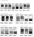
- FIG. 1 is a diagram showing scanning electron microscope observation photographs of a cross section produced by (A) the laminate manufacturing method (B) in one embodiment of the present invention, in comparison with the MSAP method of the prior art.
- (A-1) and (B-1) represent the MSAP method
- (A-2) and (B-2) represent the method of the present embodiment.
- FIG. 1B is a schematic diagram of a seed layer, in accordance with one embodiment of the present invention.
- the gray portion represents the insulating substrate layer
- the black portion represents the portion of the copper member transferred to the insulating substrate layer.
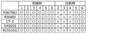
- FIG. 2 is a diagram showing the results of visual observation after the composite copper foils of Examples 1 to 6 and Comparative Examples 2 to 6 were pressure-bonded to a resin substrate and peeled off, and representative photographs of both surfaces. is. The result of visual observation is indicated by ⁇ when the surface of the copper foil is transferred to the resin side, and by ⁇ when it is not transferred.
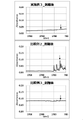
- FIG. 3 shows the results of XPS analysis of the resin substrates of Examples 1-3 and Comparative Examples 1-4.
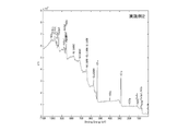
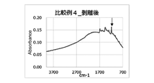
- FIG. 4 shows that the composite copper foils of Examples 1 to 3 and Comparative Examples 2 to 4 were thermally crimped to a resin substrate (R5670KJ) and peeled off, and then the surface of the composite copper foil was measured by the FT-IR/ATR method. These are the results of measurements.
- FIG. 3 shows the results of XPS analysis of the resin substrates of Examples 1-3 and Comparative Examples 1-4.
- FIG. 4 shows that the composite copper foils of Examples 1 to 3 and Comparative Examples 2 to 4 were thermally crimped
- FIG. 5 shows the results of measuring the surfaces of the composite copper foils of Example 3 and Comparative Example 3 by the FT-IR/ATR method after the composite copper foils of Example 3 and Comparative Example 3 were thermocompression bonded to a resin substrate (R1551GG) and peeled off. be.
- FIG. 6 shows that the composite copper foils of Examples 4 to 6 and Comparative Examples 5 to 6 were thermocompression bonded to a resin base material (R5680J) and peeled off, and then the surface of the composite copper foil was subjected to the FT-IR/ATR method. This is the result of the measurement.
- FIG. 7 shows the results of measuring the surfaces of the composite copper foils of Example 3 and Comparative Example 3 by the FT-IR/ATR method after the composite copper foils of Example 3 and Comparative Example 3 were thermally bonded to a resin substrate (NX9255) and then peeled off. be.
- FIG. 8 shows the composite copper foils of Example 3 and Comparative Example 3 after thermal compression bonding to the resin base material (CT-Z) and peeling, and then the surfaces of the composite copper foils were measured by the FT-IR/ATR method. This is the result.
- FIG. 9 is a secondary electron image and an EDS image of Cu obtained by analyzing the surface of the resin base material with a field emission scanning electron microscope after the composite copper foil was thermally compressed to and peeled off from the resin base material.
- FIG. 9 is a secondary electron image and an EDS image of Cu obtained by analyzing the surface of the resin base material with a field emission scanning electron microscope after the composite copper foil was thermally compressed to and peeled off from the resin base material.
- FIG. 10 shows the cross section of the seed layer formed on the resin substrate after the composite copper foils of Examples 1, 2 and 3 and Comparative Examples 3 and 7 were thermally compressed and peeled off from the resin substrate.
- FIG. 11 shows SEM images (magnification: 30,000) of cross sections of resins having seed layers of Examples 1, 2, and 3 and Comparative Example 7 that were plated.
- One embodiment of the disclosure of the present specification is a method for manufacturing a laminate of an insulating base layer and a copper member, comprising a step of bonding an insulating base layer and a copper member having protrusions on the surface; forming a seed layer by peeling off the member to transfer the projections to the surface of the insulating base layer; forming a resist on a predetermined location on the surface of the seed layer; a method of manufacturing comprising the steps of depositing copper by copper plating the areas where the resist is not deposited, removing the resist, and removing the seed layer exposed by the removal of the resist. be.
- the seed layer refers to the surface of the peeled copper member and the surface configured to include the bottom of the recesses formed in the insulating base layer by the protrusions of the copper member. Refers to the layer formed in between (FIG. 1B), so that the recess and the metal from the copper member transferred to the recess are contained within that layer.
- the bottom of the recess refers to the farthest bottom from the surface of the stripped copper member among the bottoms of the plurality of recesses, and the surface configured to include the bottom of the recess is the surface of the stripped copper member. parallel to the surface.
- Step of bonding an insulating base layer and a copper member ⁇ copper member> The surface of the copper member has fine protrusions.
- the arithmetic mean roughness (Ra) of the surface of the copper member is preferably 0.03 ⁇ m or more, more preferably 0.05 ⁇ m or more, and is preferably 0.3 ⁇ m or less, more preferably 0.2 ⁇ m or less. .
- the maximum height roughness (Rz) of the surface of the copper member is preferably 0.2 ⁇ m or more, more preferably 1.0 ⁇ m or more, and is preferably 2.0 ⁇ m or less, more preferably 1.7 ⁇ m or less. preferable.
- Ra and Rz are too small, the adhesion to the resin substrate will be insufficient, and if they are too large, fine wiring formability and high frequency characteristics will be inferior.
- Ra and Rz can be calculated by the method specified in JIS B 0601:2001 (in accordance with the international standard ISO4287-1997).
- the average length (RSm) of the surface roughness curve element of the copper member is not particularly limited, but is 1500 nm or less, 1400 nm or less, 1300 nm or less, 1200 nm or less, 1100 nm or less, 1000 nm or less, 900 nm or less, 800 nm or less, 750 nm or less, It is preferably 700 nm or less, 650 nm or less, 600 nm or less, 550 nm or less, 450 nm or less, or 350 nm or less, and preferably 100 nm or more, 200 nm or more, or 300 nm or more.
- RSm represents the average length of unevenness for one cycle included in the roughness curve at a certain reference length (lr) (that is, the length of the contour curve element: Xs1 to Xsm), It is calculated by the following formula.
- RSm can be measured and calculated according to "Method for measuring surface roughness of fine ceramic thin film by atomic force microscope (JIS R 1683:2007)".
- a layer containing copper oxide is formed on at least a part of the surface of the copper member.
- the copper member specifically includes, but is not limited to, copper foils such as electrolytic copper foil, rolled copper foil, and copper foil with a carrier, copper wires, copper plates, and copper lead frames.
- the copper member contains Cu as a main component, which is part of the structure, but a material made of pure copper with a Cu purity of 99.9% by mass or more is preferable, and is made of tough pitch copper, deoxidized copper, or oxygen-free copper. More preferably, it is made of oxygen-free copper with an oxygen content of 0.001% by mass to 0.0005% by mass.
- the copper member is a copper foil
- its thickness is not particularly limited, but is preferably 0.1 ⁇ m or more and 100 ⁇ m or less, more preferably 0.5 ⁇ m or more and 50 ⁇ m or less.
- the layer containing copper oxide is formed on the surface of the copper member and contains copper oxide (CuO) and/or cuprous oxide (Cu 2 O).
- This layer containing copper oxide can be formed by oxidizing the surface of the copper member. This oxidation treatment roughens the surface of the copper member.
- a surface roughening treatment step such as soft etching or etching is not necessary, but may be performed.
- degreasing treatment acid cleaning for uniformizing the surface by removing a natural oxide film, or alkali treatment for preventing acid from being brought into the oxidation process may be performed after acid cleaning.
- the method of alkali treatment is not particularly limited, but preferably 0.1 to 10 g/L, more preferably 1 to 2 g/L alkaline aqueous solution, such as sodium hydroxide aqueous solution, at 30 to 50 ° C. for 0.5 to 2 minutes. It should be treated to some extent.
- the oxidizing agent is not particularly limited, and for example, an aqueous solution of sodium chlorite, sodium hypochlorite, potassium chlorate, potassium perchlorate, etc. can be used.
- Various additives eg, phosphates such as trisodium phosphate dodecahydrate
- surface active molecules may be added to the oxidizing agent.
- Surface active molecules include porphyrins, porphyrin macrocycles, extended porphyrins, ring contracted porphyrins, linear porphyrin polymers, porphyrin sandwich coordination complexes, porphyrin sequences, silanes, tetraorgano-silanes, aminoethyl-aminopropyltrimethoxysilane, (3-aminopropyl)trimethoxysilane, (1-[3-(trimethoxysilyl)propyl]urea) ((l-[3-(Trimethoxysilyl)propyl]urea)), (3-aminopropyl)triethoxysilane , ((3-glycidyloxypropyl)trimethoxysilane), (3-chloropropyl)trimethoxysilane, (3-glycidyloxypropyl)trimethoxysilane, dimethyldichlorosilane, 3-(trimethoxysilyl)
- the protrusions on the surface of the oxidized copper member may be adjusted using a dissolving agent.
- the dissolving agent used in this dissolving step is not particularly limited, but is preferably a chelating agent, particularly a biodegradable chelating agent, such as ethylenediaminetetraacetic acid, diethanolglycine, tetrasodium L-glutamic acid diacetate, ethylenediamine-N,N'.
- the pH of the solution for dissolution is not particularly limited, but it is preferably alkaline, more preferably pH 8 to 10.5, still more preferably pH 9.0 to 10.5, and pH 9.8 to 10.5. 2 is more preferred.
- the surface of the layer containing copper oxide may be subjected to reduction treatment with a reducing agent, in which case cuprous oxide may be formed on the surface of the layer containing copper oxide.
- a reducing agent in which case cuprous oxide may be formed on the surface of the layer containing copper oxide.
- the reducing agent used in this reduction step include dimethylamine borane (DMAB), diborane, sodium borohydride, hydrazine and the like.
- Pure copper has a specific resistance of 1.7 ⁇ 10 -8 ( ⁇ m), while copper oxide has a specific resistance of 1 to 10 ( ⁇ m).
- Cuprous oxide is 1 ⁇ 10 6 to 1 ⁇ 10 7 ( ⁇ m), so the layer containing copper oxide has low conductivity. At most, transmission loss due to the skin effect is less likely to occur when forming a circuit of a printed wiring board or a semiconductor package substrate using the copper member according to the present invention.
- the layer containing copper oxide may contain a metal other than copper.
- the contained metal is not particularly limited, but contains at least one metal selected from the group consisting of Sn, Ag, Zn, Al, Ti, Bi, Cr, Fe, Co, Ni, Pd, Au and Pt. good too.
- metals having higher acid resistance and heat resistance than copper such as Ni, Pd, Au and Pt.
- a layer containing a metal other than copper may be formed on the layer containing copper oxide.
- This layer can be formed on the outermost surface of the copper member by plating.
- the plating method is not particularly limited. Plating can be performed by electrolytic plating, electroless plating, vacuum deposition, chemical conversion treatment, or the like, but electrolytic plating is preferred because it is preferable to form a uniform and thin plating layer.
- nickel plating and nickel alloy plating are preferable.
- Metals formed by nickel plating and nickel alloy plating include, for example, pure nickel, Ni—Cu alloy, Ni—Cr alloy, Ni—Co alloy, Ni—Zn alloy, Ni—Mn alloy, Ni—Pb alloy, Ni— P alloy etc. are mentioned.
- metal salts used for plating include nickel sulfate, nickel sulfamate, nickel chloride, nickel bromide, zinc oxide, zinc chloride, diamminedichloropalladium, iron sulfate, iron chloride, chromic anhydride, chromium chloride, sodium chromium sulfate, copper sulfate, copper pyrophosphate, cobalt sulfate, manganese sulfate, and the like;
- the bath composition is, for example, nickel sulfate (100 g/L or more and 350 g/L or less), nickel sulfamate (100 g/L or more and 600 g/L or less), nickel chloride (0 g/L or more and 300 g/L or less). and mixtures thereof are preferred, but sodium citrate (0 g/L or more and 100 g/L or less) or boric acid (0 g/L or more and 60 g/L or less) may be contained as additives.
- the copper oxide on the surface is first reduced, and an electric charge is used to turn it into cuprous oxide or pure copper. After that, the metal that forms the metal layer begins to deposit.
- the amount of charge varies depending on the type of plating solution and the amount of copper oxide. For example, when Ni plating is applied to a copper member, 10 C per area dm 2 of the copper member to be electrolytically plated is required to keep the thickness within a preferable range. It is preferable to apply an electric charge of 90C or more, and it is more preferable to apply an electric charge of 20C or more and 65C or less.
- the amount of metal deposited on the outermost surface of the copper member by plating is not particularly limited, it is preferably 0.8 to 6.0 mg/dm 2 .
- the amount of adhered metal can be calculated by, for example, dissolving in an acidic solution, measuring the amount of metal by ICP analysis, and dividing the amount by the plane visual field area of the structure.
- the surface of the copper member is partially coated with a coating agent such as a silane coupling agent or an antiseptic before the oxidation treatment; Steps such as treating the oxide-containing layer with a dissolving agent may be performed.
- a coating agent such as a silane coupling agent or a preservative
- the portion is prevented from being subjected to oxidation treatment, and voids are generated in the layer containing copper oxide, and the copper is removed from the copper member.
- Layers containing oxides tend to break.
- the dissolving agent is an agent that dissolves copper oxide, and by treating with the dissolving agent, the copper oxide near the interface between the copper member and the layer containing copper oxide is partially dissolved, The layer containing copper oxide is likely to break from the copper member.
- Silane coupling agents are not particularly limited, but silane, tetraorgano-silane, aminoethyl-aminopropyltrimethoxysilane, (3-aminopropyl)trimethoxysilane, (1-[3-(trimethoxysilyl)propyl]urea ) ((l-[3-(Trimethoxysilyl)propyl]urea)), (3-aminopropyl)triethoxysilane, ((3-glycidyloxypropyl)trimethoxysilane), (3-chloropropyl)trimethoxysilane, (3-glycidyloxypropyl)trimethoxysilane, dimethyldichlorosilane, 3-(trimethoxysilyl)propyl methacrylate, ethyltriacetoxysilane, triethoxy(isobutyl)silane, triethoxy(octyl)silane
- Rust inhibitors are not particularly limited, but 1H-tetrazole, 5-methyl-1H-tetrazole, 5-amino-1H-tetrazole, 5-phenyl-1H-tetrazole, 1,2,3-triazole, 1,2,4 -triazole, 1,2,3-benzotriazole, 5-methyl-1H-benzotriazole, 5-amino-1H-benzotriazole, 2-mercaptobenzothiazole, 1,3-dimethyl-5-pyrazolone, pyrrole, 3- methylpyrrole, 2,4-dimethylpyrrole, 2-ethylpyrrole, pyrazole, 3-aminopyrazole, 4-methylpyrazole, 3-amino-5-hydroxypyrazole, thiazole, 2-aminothiazole, 2-methylthiazole, 2- amino-5-methylthiazole, 2-ethylthiazole, benzothiazole, imidazole, 2-methylimidazole, 2-ethylimid
- the treatment with a silane coupling agent or antiseptic may be performed at any time before the oxidation treatment, such as degreasing, acid cleaning for uniform treatment by removing the native oxide film, or acid to the oxidation process after acid cleaning.
- the dissolving agent for making it easier to break the layer containing copper oxide from the copper member is not limited to Ni chloride, as long as it contains a component that dissolves copper oxide, and chlorides (potassium chloride, zinc chloride , iron chloride, chromium chloride, etc.), ammonium salts (ammonium citrate, ammonium chloride, ammonium sulfate, nickel ammonium sulfate, etc.), chelating agents (ethylenediaminetetraacetic acid, diethanolglycine, L-glutamic acid diacetic acid/tetrasodium, ethylenediamine-N, N'-disuccinic acid, sodium 3-hydroxy-2,2'-iminodisuccinate, trisodium methylglycine diacetate, tetrasodium aspartate diacetate, disodium N-(2-hydroxyethyl)iminodiacetate, sodium gluconate etc.), tin(II) chloride, and citric acid.
- the copper member on which the layer containing copper oxide is formed is immersed in a Ni chloride solution (concentration of 45 g/L or more) at room temperature or at a temperature higher than room temperature for 5 seconds or more. is preferred.
- a Ni chloride solution concentration of 45 g/L or more
- treatment may be performed simultaneously with oxidation treatment, or treatment may be performed simultaneously with plating treatment after oxidation treatment.
- Ni chloride is contained in the plating solution, and a layer containing copper oxide is formed in the plating solution for 5 seconds, 10 seconds, 15 seconds, 20 seconds, 30 seconds, 1 minute, or 2 minutes before plating.
- the formed copper member may be immersed.
- the immersion time can be appropriately changed depending on the oxide film thickness.
- the base material of the insulating base material layer should be such that when the surface of the copper member on which the unevenness is formed is bonded to the insulating base material layer, the surface profile including the uneven shape of the copper member is transferred to the resin base material.
- a resin substrate is preferable.
- the resin base material is a material containing resin as a main component, but the type of resin is not particularly limited, and may be a thermoplastic resin or a thermosetting resin, polyphenylene ether (PPE), Epoxy, polyphenylene oxide (PPO), polybenzoxazole (PBO), polytetrafluoroethylene (PTFE), liquid crystal polymer (LCP), thermoplastic polyimide (TPI), fluororesin, polyetherimide, polyetheretherketone, polycyclo Olefins, bismaleimide resins, low dielectric constant polyimides, cyanate resins, or mixed resins thereof can be exemplified.
- the resin base material may further contain an inorganic filler or glass fiber.
- the dielectric constant of the insulating substrate layer used is preferably 5.0 or less, more preferably 4.0 or less, and even more preferably 3.8 or less.
- the bonding method is not particularly limited, but thermal press fitting is preferred.
- the resin base material and the copper member may be adhered and laminated, and then heat treated under predetermined conditions.
- predetermined conditions eg, temperature, pressure, time, etc.
- Predetermined conditions include, for example, the following conditions.
- a copper member is heated to the resin base material by applying a pressure of 0 to 20 MPa at a temperature of 50 ° C. to 300 ° C. for 1 minute to 5 hours. Crimping is preferred.
- the resin substrate is GX13 (manufactured by Ajinomoto Fine-Techno Co., Ltd.), it is heated while being pressurized at 1.0 MPa and held at 180° C. for 60 minutes for thermocompression bonding.
- the resin base material contains or consists of a PPE resin
- a copper member is attached to the resin base material by applying a pressure of 0 to 20 MPa at a temperature of 50° C. to 350° C. for 1 minute to 5 hours. Thermocompression bonding is preferred.
- the resin substrate is R5620 (manufactured by Panasonic)
- the temperature and pressure are increased to 2.0 to 3.0 MPa after thermocompression bonding while heating to 100 ° C. under a pressure of 0.5 MPa. , 200 to 210° C. for 120 minutes for further thermocompression bonding.
- the temperature and pressure are increased to 3.0 to 4.0 MPa after thermocompression bonding while heating to 110 ° C. under a pressure of 0.5 MPa. , and 195° C. for 75 minutes for thermocompression bonding.
- the heat of the copper member is applied to the resin base material by applying a pressure of 0 to 20 MPa at a temperature of 50 ° C. to 400 ° C. for 1 minute to 5 hours. Crimping is preferred.
- a copper member is formed on the resin substrate by applying a pressure of 0 to 20 MPa at a temperature of 50 ° C. to 400 ° C. for 1 minute to 5 hours.
- Heat crimping is preferred.
- the resin substrate is CT-Z (manufactured by Kuraray)
- it is heated under a pressure of 0 MPa, held at 260 ° C. for 15 minutes, further heated while being pressurized at 4 MPa, and held at 300 ° C. for 10 minutes. heat press.
- Step of peeling off the copper member After the copper member is attached to the insulating base layer, when the copper member is peeled off from the insulating base layer under predetermined conditions, the protrusions on the surface of the copper member are removed from the insulating base layer. to form a seed layer on the surface of the insulating base layer. Therefore, the surface of the insulating base layer becomes flat.
- the thickness of the seed layer may be 2.50 ⁇ m or less, more preferably 2.00 ⁇ m or less, and even more preferably 1.70 ⁇ m or less. Moreover, it is preferably 0.01 ⁇ m or more, more preferably 0.10 ⁇ m or more, and even more preferably 0.36 ⁇ m or more. If the thickness is less than 0.01 ⁇ m, the plating formability is poor and the adhesion to the insulating substrate is lowered. If it exceeds 2.50 ⁇ m, the wiring formability is deteriorated.
- the method for measuring the thickness of the seed layer is not particularly limited, and for example, the thickness of the seed layer may be measured in the SEM image.
- the seed layer thus produced is used as it is as part of the circuit.
- the adhesion between the copper and the insulating base layer is improved.
- the conditions for peeling off the copper member from the insulating base layer are not particularly limited, but a 90° peeling test (Japanese Industrial Standards (JIS) C5016 "Flexible printed wiring board test method"; corresponding international standards IEC249-1: 1982, IEC326- 2:1990).
- the method of peeling off the copper member from the insulating base material layer is not particularly limited, but a machine may be used, or a manual operation may be performed.
- the metal transferred to the surface of the insulating substrate layer after peeling off the copper member can be analyzed by various methods (e.g., X-ray photoelectron spectroscopy (XPS), energy dispersive X-ray spectroscopy (EDS), ICP emission spectroscopy). (Inductively Coupled Plasma Emission Spectroscopy, ICP-OES/ICP-AES)).
- XPS X-ray photoelectron spectroscopy
- EDS energy dispersive X-ray spectroscopy
- ICP emission spectroscopy ICP emission spectroscopy
- ICP-OES/ICP-AES Inductively Coupled Plasma Emission Spectroscopy
- XPS is a technique for performing energy analysis by irradiating an object with X-rays and capturing photoelectrons e ⁇ emitted as the object is ionized.
- XPS it is possible to examine the types, abundances, chemical bonding states, etc. of elements present on the surface of the sample or from the surface to a predetermined depth (for example, up to a depth of 6 nm).
- the diameter of the analysis spot (that is, the diameter of the cross section of the cylindrical portion that can be analyzed so that the cross section is circular) is suitably 1 ⁇ m or more and 1 mm or less.
- the metal atoms contained in the layer containing copper oxide may be detected from the surface of the insulating base material from which the copper member has been peeled off by XPS Survey spectrum analysis.
- the metal contained in the convex part of the copper member is insulated so as to fill 70% or more, 80% or more, 90% or more, 95% or more, 99% or more, or 99.9% or more of the concave part of the transferred surface profile. Transfer to the substrate layer is preferred.
- the metal fills most of the recesses in the insulating base layer, when the surface of the insulating base layer is measured by XPS, the total peak intensity of the main peaks of the spectrum of metal atoms is higher than the peak intensity of the main peak of the spectrum of C1s. will also grow.
- the main peak is the peak with the highest intensity among multiple peaks of the metal element.
- Cu is 2p3 orbital
- Sn is 3d5 orbital
- Ag is 3d5 orbital
- Zn is 2p3 orbital
- Al is 2p orbital
- Ti is 2p3 orbital
- Bi is 4f7 orbital
- Cr is 2p3 orbital
- Fe is 2p3 orbital
- Co is 2p3
- the main peak is the 2p3 orbital of Ni, the 3d5 orbital of Pd, the 4f7 orbital of Au, and the 4f7 orbital of Pt.
- the peak intensity of the spectrum referred to here means the height in the vertical axis direction of the XPS spectrum data.
- the ratio of Cu2p3 to the total atoms on the surface of the insulating base layer from which the copper member is peeled off, as measured by XPS, is 1.0 atom% or more, 1.8 atom% or more, 2.8 atom% or more, 3.0 atom% or more, It is preferably 4.0 atom % or more, 5.0 atom % or more, or 6.0 atom %.
- the ratio of the surface atomic composition percentage of Cu2p3 / the surface atomic composition percentage of C1s is 0.010 or more, 0.015 or more, 0.020 or more, 0 It is preferably 0.025 or more, 0.030 or more, 0.035 or more, 0.040 or more, 0.045 or more, 0.050 or more, or 0.10 or more.
- the total atomic composition percentage of the metal atoms on the surface of the peeled insulating base layer measured by X-ray photoelectron spectroscopy (XPS) is 1.0 atom. % or more, 1.5 atom % or more, 1.8 atom % or more, 2.8 atom % or more, 3.0 atom % or more, 4.0 atom % or more, 5.0 atom % or more, or 6.0 atom %.
- the value of the ratio of (total atomic composition percentage of metal atoms on the surface of the peeled insulating base layer):(atomic composition percentage of C1s on the surface of the peeled insulating base layer) is 0.010. 0.015 or more, 0.020 or more, 0.025 or more, 0.030 or more, 0.035 or more, 0.040 or more, 0.045 or more, 0.050 or more, or 0.10 or more preferable.
- the ratio of Cu should be 1 atom% or more, preferably 4 atom% or more, and 7 atom% or more. It is more preferably 10 atom % or more, further preferably 11.4 atom % or more.
- the transfer efficiency indicates the rate at which the metal contained in the protrusions formed on the copper member is transferred to the insulating base layer.
- composition ratio of the sum of the metals on the surface of the insulating base layer from which the copper member has been peeled off/(C+O) measured by EDS may be 0.38 or more, preferably 0.40 or more. , is more preferably 0.42 or more, and more preferably 0.43 or more.
- the amount of substances derived from the insulating base layer detected from the surface of the copper member peeled off from the insulating base layer is preferably below the detection limit or, if detected, is a small amount. This is because, in that case, when the copper member is peeled off, breakage in the insulating base material layer can be sufficiently suppressed.
- the method for detecting substances derived from the insulating base layer is not particularly limited, and a method suitable for the target substance may be used. For example, in the case of organic substances, attenuated total reflection absorption Fourier transform infrared spectroscopy (FT-IR method) ("Infrared and Raman Spectroscopy: Principles and Spectral Interpretation" by Peter Larkin).
- the FT - IR method is an infrared spectroscopic method in which the substance to be measured is irradiated with infrared rays, and the compound is identified and / or quantified using the infrared absorption spectrum.
- the N ratio is preferably 10 or less and 9 or less, more preferably 8 or less and 7 or less, and preferably no peak derived from the resin substrate is detected.
- the ratio of Ra after peeling to Ra before bonding on the surface of the copper member on which the layer having the protrusions is formed is less than 100%, less than 96%, less than 95%, less than 94%, less than 93%, and 92%. preferably less than, less than 91%, less than 90%, less than 80%, less than 70%, less than 65% or less than 60%.
- a smaller ratio means that the metal forming the layer having protrusions transferred to the insulating base layer.
- the ratio of the surface area after peeling to the surface area before bonding of the copper member on which the layer having the convex portion is formed is less than 100%, less than 98%, less than 97%, less than 96%, less than 95%, less than 94%. , less than 93%, less than 92%, less than 91%, less than 90%, less than 80% or less than 75%.
- a smaller ratio means that the metal forming the layer having protrusions transferred to the insulating base layer.
- the surface area can be measured using a confocal microscope or an atomic force microscope.
- ⁇ E * ab between the surface of the copper member before thermocompression bonding and the surface of the copper member after peeling is 13 or more, 15 or more, 20 or more, 25 or more, 30 or more, or 35 or more. It means that the larger the difference, the more the metal forming the protrusions transferred to the insulating base layer.
- the adhesiveness between the resin substrate and the seed layer is enhanced by forming irregularities that serve as anchors in the resin.
- relatively large unevenness was formed on the surface to ensure adhesion, but this caused copper to precipitate deep from the resin surface layer, so when the seed layer was etched and removed, a small amount of copper remained. tended to A deep etching process was necessary because this trace amount of remaining copper could cause a short circuit between wirings.
- the effect of increasing adhesion by unevenness forming treatment and electroless copper plating film is that selectivity to resin substrates is high, and sufficient adhesion effect can be obtained only in some cases such as ABF (Ajinomoto Build-Up Film). It is only a resin base material.
- an ultra-thin copper foil with a carrier is used, but the thickness of the ultra-thin copper foil layer must be 1.5 ⁇ m or more from the viewpoint of handling, etc.
- roughening treatment of 1 ⁇ m or more is performed. ing.
- the adhesion between the resin substrate and the seed layer is enhanced.
- a deep etching process was required.
- the seed layer obtained by the method of the present disclosure has a smaller surface roughness than the case where the surface is roughened by desmear treatment in the conventional SAP method or the case where the ultra-thin copper foil with a carrier is roughened in the conventional MSAP method. Also, it is possible to avoid problems such as residual copper after etching, pattern skipping due to side etching in fine patterns, and transmission loss of high-frequency signals due to unevenness. In addition, although the surface roughness is small, fine unevenness is densely present, so that the insulating base material and copper are sufficiently adhered to each other.
- the resist may contain, for example, a material that is cured or dissolved by exposure to light, and is not particularly limited, but is preferably formed of a dry film resist (DFR), a positive liquid resist, or a negative liquid resist.
- DFR dry film resist
- DFR preferably contains a binder polymer that contributes to film formability, a monomer that undergoes a photopolymerization reaction upon UV irradiation (for example, an acrylic ester-based or methacrylic ester-based monomer), and a photopolymerization initiator.
- a dry film having a three-layer structure of cover form/photoresist/carrier film is preferably used for forming the DFR.
- a DFR, which is a resist can be formed on the structure by laminating the photoresist on the structure while peeling off the cover film, and then peeling off the carrier film after the lamination.
- Liquid resists include novolak resins that are soluble in organic solvents.
- the resist can be formed by coating the surface of the structure, drying it, and then dissolving or curing the resist by light irradiation.
- the thickness of the resist is not particularly limited, it is preferably 1 ⁇ m to 200 ⁇ m.
- the surface of the seed layer may be plated to form a second seed layer.
- the method of plating treatment is not particularly limited, and may be electrolytic plating or electroless plating.
- a film may be formed by a plating method.
- the second seed layer refers to a metal thin film formed by plating.
- the thickness of the second seed layer is not particularly limited, and may be about 0.02 to 2 ⁇ m. .
- the method of copper plating treatment is not particularly limited, and plating treatment can be performed using a known method.
- the method of removing the resist is not particularly limited, and known methods such as a method using fuming nitric acid or sulfuric acid-hydrogen peroxide mixture, and a dry ashing method using O 2 plasma or the like can be used.
- Step of Removing Seed Layer The method for removing the seed layer is not particularly limited, and known methods such as quick etching and flash etching using a sulfuric acid-hydrogen peroxide-based etchant can be used.
- One embodiment of the present invention is a method for selecting a copper member having a layer containing copper oxide formed on at least part of the surface thereof, wherein the copper member is thermally compressed to a resin base material and then pulled from the resin base material.
- a step of peeling a step of analyzing the surface of the copper member peeled off from the resin base material by attenuated total reflection absorption Fourier transform infrared spectroscopy (FT-IR / ATR method), and a resin base material with the copper member peeled off.
- FT-IR / ATR method attenuated total reflection absorption Fourier transform infrared spectroscopy
- a step of performing EDS elemental analysis on the surface of the copper member a step of measuring the thickness of the seed layer formed on the resin base material from which the copper member is peeled off, and a copper member obtained by the FT-IR / ATR method.
- the S/N ratio of the peak corresponding to the substance derived from the resin substrate on the surface is 10 or less in the wavelength range 700-4000 cm -1 , and the total metal on the surface of the copper member obtained by EDS elemental analysis / ( C+O) composition ratio is 0.4 or more, and the thickness of the seed layer is 0.1 ⁇ m or more and 2.0 ⁇ m or less, selecting a copper member.
- Another embodiment of the present invention is a method for selecting a copper member having a layer containing copper oxide formed on at least part of the surface thereof, wherein the copper member is thermally compressed to a resin base material, and then A step of peeling off, a step of performing Survey spectrum analysis of X-ray photoelectron spectroscopy (XPS) on the surface of the copper member peeled off from the resin substrate, and a surface of the resin substrate from which the copper member was peeled off , a step of performing EDS elemental analysis, a step of measuring the thickness of the seed layer formed on the resin base material from which the copper member has been peeled off, and The composition ratio of total metal on the surface of the copper member/(C+O) detected from the surface of the peeled resin base material and obtained by EDS elemental analysis is 0.4 or more, and the thickness of the seed layer is 0.4. selecting a copper member having a thickness of 1 ⁇ m or more and 2.0 ⁇ m or less.
- XPS X-ray photoelectron
- Each step can be performed according to the details described in the manufacturing method of the laminate.
- this selection method it is possible to select a copper member having good plating and wiring forming properties when a circuit is formed.
- Comparative Example 7 an ultra-thin copper foil with a carrier (MT18FL, ultra-thin copper foil thickness: 1.5 ⁇ m) manufactured by Mitsui Mining & Smelting Co., Ltd. was used as it was. In addition, Comparative Example 1 does not use a composite copper foil as described later.
- MT18FL ultra-thin copper foil thickness: 1.5 ⁇ m
- Example 1 potassium carbonate 2.5 g / L; KBE-903 (3-aminopropyltriethoxysilane; manufactured by Shin-Etsu Silicone Co., Ltd.) 1 vol%
- Example 3 contains 2.5 g/L of potassium carbonate; 0.06 g/L of potassium bicarbonate;
- Examples 4 to 6 contain 5 g/L of potassium hydroxide
- Comparative Example 2 is a solution of 2.5 g/L of potassium carbonate
- Comparative Example 3 is a solution of potassium carbonate 2.5 g / L; potassium hydrogen carbonate 0.06 g / L;
- Comparative Example 5 is potassium hydroxide 5 g / L; KBM-603 (N-2-(aminoethyl)-3 -Aminopropyltrimethoxysilane; manufactured by Shin-Etsu Silicone Co., Ltd.) 5 vol%
- Comparative Example 6 contains potassium hydroxide
- Comparative Example 3 contains sodium chlorite 58.8 g/L as an oxidizing agent; potassium hydroxide 8.8 g/L; potassium carbonate 3 g/L; KBM-403 (3-glycidoxypropyltrimethoxysilane; Shin-Etsu Silicone Co., Ltd.) 2 g/L solution was used.
- Examples 1 and 2 and Comparative Examples 5 and 6 were immersed in the oxidizing agent at 73° C. for 6 minutes, and Examples 3 to 6 and Comparative Examples 2 and 3 were immersed in the oxidizing agent at 73° C. for 2 minutes.
- Example 4 was treated at 45° C. for 10 seconds using a solution of 45 g/L of tin(II) chloride dihydrate and 1 mL/L of hydrochloric acid.
- Example 5 was treated at 45° C. for 60 seconds using a solution of 45 g/L of ammonium chloride.
- Example 6 was treated at 45° C. for 60 seconds using a 50% citric acid solution of 45 mL/L.
- a laminate sample was obtained by laminating prepreg on a test piece and thermocompression bonding in a vacuum using a vacuum high pressure press.
- the resin base material is R5670KJ (manufactured by Panasonic)
- the temperature and pressure are increased to 2.94 MPa and 210° C. for 120 minutes after thermocompression bonding while heating to 110° C. under a pressure of 0.49 MPa. It was thermocompression bonded by holding.
- the resin base material is R5680J (manufactured by Panasonic) after heat-pressing while heating to 110 ° C. under a pressure of 0.5 MPa, the temperature and pressure are increased, and held for 75 minutes at 3.5 MPa and 195 ° C. It was thermocompression bonded by doing.
- the resin substrate is NX9255 (manufactured by Park Electrochemical)
- it is heated to 260°C while pressurizing at 0.69 MPa, and the pressure is increased to 1.5 MPa and heated to 385°C. It was thermocompression bonded by holding for 1 minute.
- the resin substrate is R1551GG (manufactured by Panasonic)
- it is heated under a pressure of 1 MPa, and after reaching 100 ° C., it is held at that temperature for 10 minutes, and then further heated under a pressure of 3.3 MPa to 180 ° C. After the temperature was reached, the temperature was maintained for 50 minutes for thermocompression bonding.
- the resin substrate is CT-Z (manufactured by Kuraray Co., Ltd.), it is heated under a pressure of 0 MPa, held at 260° C. for 15 minutes, further heated while being pressurized at 4 MPa, and held at 300° C. for 10 minutes. crimped.
- the copper member was peeled off from the resin substrate according to the 90° peeling test (Japanese Industrial Standards (JIS) C5016) for these laminate samples (Fig. 1). Visual observation results are shown in Figure 2-1. Photographs of the surfaces of the resin side and the copper foil side after peeling off are shown in Fig. 2-2 for representative combinations.
- Example 1 since the composite copper foil was not plated, only Cu atoms were transferred and detected on the resin substrate side. In Examples 2 and 3, since Ni plating was performed, Cu atoms and Ni atoms were transferred and detected on the resin side.
- the ratio of C1s was smaller in both Examples and Comparative Examples 5 and 6 than in Comparative Examples 1 to 4. In the examples, it is believed that the proportion of C1s on the surface was relatively decreased due to the transfer of cupric oxide or cuprous oxide.
- R1551GG When using R1551GG as a resin base material, it is around 1200 cm -1 , when using R5670KJ and R5680J, it is around 1190 cm -1 , when using NX9255, it is around 1232 cm -1, and when CT - Z is used, it is 1741 cm -1 .
- the maximum peak detectable wavelength was taken to be around 1 (the arrows in FIGS. 4 to 8 indicate the maximum peak detectable wavelength).
- the S/N ratio was calculated using the noise value (N) as the difference between the maximum and minimum values of the peaks detected at a wavelength of 3800-3850 cm ⁇ 1 .
- Elemental Analysis by EDS (Energy Dispersive X-ray Spectrometer)> First, elemental analysis was performed using an EDS (energy dispersive X-ray spectroscope) (manufactured by Oxford, trade name: X-Max Extreme) (conditions: acceleration voltage of 10 kV, magnification of 30,000 times).
- FIG. 9 shows a typical secondary electron image and an EDS elemental mapping image of Cu
- Table 6 (Example) and Table 7 (Comparative Example) show the ratio of each element of C, O, Ni, Cu, and Sn ( atom %), and the value of the ratio (sum of ratios of metal elements/(sum of ratios of C and O)) calculated from these values.
- the ratio of Cu is 10 atom % or more, and Cu transfers at a high ratio, and (the sum of the ratios of metal elements/(the sum of the ratios of C and O)) is 0.4 or more. , good plating formability.
- the proportion of Cu was 0.1 atom % or less, and almost no Cu was transferred, resulting in poor plating formability.
- Comparative Examples 5 and 6 (the sum of the proportions of the metal elements/(the sum of the proportions of C and O)) is as low as less than 0.4, and these are also poor in plating formability.
- the resin having a seed layer produced using the composite copper foil of the example has good plating formability in terms of surface element composition.
- Seed layer thickness The thickness of the seed layer was then measured. Specifically, in the cross section of SEM (magnification: 10,000 times), for the layer in which the copper protrusions are embedded in the resin base material, the upper side corresponding to the upper surface of the layer and the lower side corresponding to the lower surface of the layer are in contact with each other. The maximum distance between two parallel straight lines was examined, and the distance was taken as the thickness of the seed layer.
- FIG. 10 shows a representative SEM image, and Tables 6 and 7 show the thickness measurement results.
- the wiring formability is good.
- Comparative Examples 2 and 3 since the thickness of the seed layer was 0 ⁇ m and metal transfer did not occur, almost no plating was formed.
- Comparative Example 7 since the seed layer is too thick, it is difficult to miniaturize the circuit, and the wiring formability is also poor as shown in ⁇ 3> below.
- the resin having a seed layer produced using the composite copper foil of the example has good wiring formability in terms of the thickness of the seed layer.
- electrolytic copper plating was performed at a current density of 1 A/dm 2 at 30° C. for 30 minutes to form an electrolytic copper plating film with a thickness of 15 ⁇ m.
- the seed layer under the plating resist was dissolved and removed by etching using a mixed solution of sulfuric acid and hydrogen peroxide to obtain a laminated wiring circuit board.
- the resin having the seed layer of Example 3 was subjected to electroplating alone to form a second seed layer. Specifically, using a commercially available electrolytic copper plating solution, an electrolytic copper plating film was formed at a current density of 1 A/dm 2 at 30°C.
- FIG. 11 shows SEM cross-sectional images (30000 times) of Examples 1, 2 and 3 and Comparative Example 7.
- electrolytic copper plating was performed at a current density of 1 A/dm 2 at 30° C. for 30 minutes to form an electrolytic copper plating film with a thickness of 15 ⁇ m.
- the seed layer under the plating resist was dissolved and removed by etching using a mixed solution of sulfuric acid and hydrogen peroxide to obtain a laminated wiring circuit board.
- Comparative Example 7 has a low etching factor and poor wiring formability.
Landscapes
- Chemical & Material Sciences (AREA)
- Engineering & Computer Science (AREA)
- Materials Engineering (AREA)
- Chemical Kinetics & Catalysis (AREA)
- Metallurgy (AREA)
- Organic Chemistry (AREA)
- Mechanical Engineering (AREA)
- Electrochemistry (AREA)
- Microelectronics & Electronic Packaging (AREA)
- General Chemical & Material Sciences (AREA)
- Manufacturing & Machinery (AREA)
- Laminated Bodies (AREA)
- Other Surface Treatments For Metallic Materials (AREA)
Priority Applications (3)
| Application Number | Priority Date | Filing Date | Title |
|---|---|---|---|
| JP2023516361A JPWO2022224684A1 (https=) | 2021-04-20 | 2022-03-23 | |
| KR1020237021593A KR20230170899A (ko) | 2021-04-20 | 2022-03-23 | 구리 부재 |
| CN202280008657.5A CN116670326A (zh) | 2021-04-20 | 2022-03-23 | 铜部件 |
Applications Claiming Priority (2)
| Application Number | Priority Date | Filing Date | Title |
|---|---|---|---|
| JP2021-071460 | 2021-04-20 | ||
| JP2021071460 | 2021-04-20 |
Publications (1)
| Publication Number | Publication Date |
|---|---|
| WO2022224684A1 true WO2022224684A1 (ja) | 2022-10-27 |
Family
ID=83722285
Family Applications (1)
| Application Number | Title | Priority Date | Filing Date |
|---|---|---|---|
| PCT/JP2022/013649 Ceased WO2022224684A1 (ja) | 2021-04-20 | 2022-03-23 | 銅部材 |
Country Status (5)
| Country | Link |
|---|---|
| JP (1) | JPWO2022224684A1 (https=) |
| KR (1) | KR20230170899A (https=) |
| CN (1) | CN116670326A (https=) |
| TW (1) | TW202311563A (https=) |
| WO (1) | WO2022224684A1 (https=) |
Families Citing this family (2)
| Publication number | Priority date | Publication date | Assignee | Title |
|---|---|---|---|---|
| TWI822620B (zh) * | 2023-03-24 | 2023-11-11 | 景碩科技股份有限公司 | 銅箔基板的前處理方法 |
| TWI876554B (zh) * | 2023-09-26 | 2025-03-11 | 南亞塑膠工業股份有限公司 | 銅箔的表面處理方法、抗氧化銅箔、及鋰電池的負極 |
Citations (5)
| Publication number | Priority date | Publication date | Assignee | Title |
|---|---|---|---|---|
| JP2000036660A (ja) * | 1998-07-17 | 2000-02-02 | Hitachi Chem Co Ltd | ビルドアップ多層配線板の製造方法 |
| WO2015040998A1 (ja) * | 2013-09-20 | 2015-03-26 | 三井金属鉱業株式会社 | 銅箔、キャリア箔付銅箔及び銅張積層板 |
| WO2017056534A1 (ja) * | 2015-09-30 | 2017-04-06 | 三井金属鉱業株式会社 | 粗化処理銅箔、銅張積層板及びプリント配線板 |
| WO2019244541A1 (ja) * | 2018-06-20 | 2019-12-26 | ナミックス株式会社 | 粗化処理銅箔、銅張積層板及びプリント配線板 |
| JP6806405B1 (ja) * | 2020-04-27 | 2021-01-06 | ナミックス株式会社 | 複合銅部材 |
Family Cites Families (2)
| Publication number | Priority date | Publication date | Assignee | Title |
|---|---|---|---|---|
| CN109951964A (zh) * | 2013-07-23 | 2019-06-28 | Jx日矿日石金属株式会社 | 表面处理铜箔、附载体铜箔、基材、及树脂基材 |
| KR101701103B1 (ko) * | 2015-03-12 | 2017-02-01 | 주식회사 두하누리 | 금속과 고분자 간 접착 방법 및 이를 이용한 기판 |
-
2022
- 2022-03-23 JP JP2023516361A patent/JPWO2022224684A1/ja active Pending
- 2022-03-23 WO PCT/JP2022/013649 patent/WO2022224684A1/ja not_active Ceased
- 2022-03-23 KR KR1020237021593A patent/KR20230170899A/ko active Pending
- 2022-03-23 CN CN202280008657.5A patent/CN116670326A/zh active Pending
- 2022-03-29 TW TW111111931A patent/TW202311563A/zh unknown
Patent Citations (5)
| Publication number | Priority date | Publication date | Assignee | Title |
|---|---|---|---|---|
| JP2000036660A (ja) * | 1998-07-17 | 2000-02-02 | Hitachi Chem Co Ltd | ビルドアップ多層配線板の製造方法 |
| WO2015040998A1 (ja) * | 2013-09-20 | 2015-03-26 | 三井金属鉱業株式会社 | 銅箔、キャリア箔付銅箔及び銅張積層板 |
| WO2017056534A1 (ja) * | 2015-09-30 | 2017-04-06 | 三井金属鉱業株式会社 | 粗化処理銅箔、銅張積層板及びプリント配線板 |
| WO2019244541A1 (ja) * | 2018-06-20 | 2019-12-26 | ナミックス株式会社 | 粗化処理銅箔、銅張積層板及びプリント配線板 |
| JP6806405B1 (ja) * | 2020-04-27 | 2021-01-06 | ナミックス株式会社 | 複合銅部材 |
Also Published As
| Publication number | Publication date |
|---|---|
| KR20230170899A (ko) | 2023-12-19 |
| TW202311563A (zh) | 2023-03-16 |
| JPWO2022224684A1 (https=) | 2022-10-27 |
| CN116670326A (zh) | 2023-08-29 |
Similar Documents
| Publication | Publication Date | Title |
|---|---|---|
| US12336116B2 (en) | Composite copper components | |
| JP7127861B2 (ja) | 複合銅箔 | |
| WO2022224684A1 (ja) | 銅部材 | |
| TWI878462B (zh) | 具有空隙之複合銅構件、附載體金屬箔、積層體、印刷佈線板的製造方法、樹脂基材的製造方法及複合銅構件的製造方法 | |
| JP7810445B2 (ja) | 複合銅部材の製造システム | |
| JP7352939B2 (ja) | 複合銅部材 | |
| WO2022202921A1 (ja) | 積層体の製造方法 | |
| US12604416B2 (en) | Laminate for wiring board | |
| KR102931323B1 (ko) | 복합 구리 배선 및 레지스트층을 갖는 적층체 | |
| TWI918818B (zh) | 銅構件、印刷佈線板用導體、印刷佈線板用構件、印刷佈線板、印刷電路板及該等的製造方法 | |
| TW202226911A (zh) | 銅構件、印刷佈線板用導體、印刷佈線板用構件、印刷佈線板、印刷電路板及該等的製造方法 | |
| TW202316919A (zh) | 金屬構件 |
Legal Events
| Date | Code | Title | Description |
|---|---|---|---|
| 121 | Ep: the epo has been informed by wipo that ep was designated in this application |
Ref document number: 22791461 Country of ref document: EP Kind code of ref document: A1 |
|
| ENP | Entry into the national phase |
Ref document number: 2023516361 Country of ref document: JP Kind code of ref document: A |
|
| WWE | Wipo information: entry into national phase |
Ref document number: 202280008657.5 Country of ref document: CN |
|
| NENP | Non-entry into the national phase |
Ref country code: DE |
|
| 122 | Ep: pct application non-entry in european phase |
Ref document number: 22791461 Country of ref document: EP Kind code of ref document: A1 |