WO2022224684A1 - Copper member - Google Patents
Copper member Download PDFInfo
- Publication number
- WO2022224684A1 WO2022224684A1 PCT/JP2022/013649 JP2022013649W WO2022224684A1 WO 2022224684 A1 WO2022224684 A1 WO 2022224684A1 JP 2022013649 W JP2022013649 W JP 2022013649W WO 2022224684 A1 WO2022224684 A1 WO 2022224684A1
- Authority
- WO
- WIPO (PCT)
- Prior art keywords
- copper
- copper member
- base material
- resin base
- layer containing
- Prior art date
Links
- RYGMFSIKBFXOCR-UHFFFAOYSA-N Copper Chemical compound [Cu] RYGMFSIKBFXOCR-UHFFFAOYSA-N 0.000 title claims abstract description 369
- 239000010949 copper Substances 0.000 title claims abstract description 316
- 229910052802 copper Inorganic materials 0.000 title claims abstract description 302
- 229920005989 resin Polymers 0.000 claims abstract description 200
- 239000011347 resin Substances 0.000 claims abstract description 200
- 239000000463 material Substances 0.000 claims abstract description 112
- 238000000034 method Methods 0.000 claims abstract description 91
- 229910052751 metal Inorganic materials 0.000 claims abstract description 78
- QPLDLSVMHZLSFG-UHFFFAOYSA-N Copper oxide Chemical compound [Cu]=O QPLDLSVMHZLSFG-UHFFFAOYSA-N 0.000 claims abstract description 72
- 239000002184 metal Substances 0.000 claims abstract description 71
- 239000005751 Copper oxide Substances 0.000 claims abstract description 69
- 229910000431 copper oxide Inorganic materials 0.000 claims abstract description 69
- 238000005033 Fourier transform infrared spectroscopy Methods 0.000 claims abstract description 27
- 238000000921 elemental analysis Methods 0.000 claims abstract description 20
- 239000000126 substance Substances 0.000 claims abstract description 16
- 238000010521 absorption reaction Methods 0.000 claims abstract description 8
- 238000005102 attenuated total reflection Methods 0.000 claims abstract description 8
- 239000000758 substrate Substances 0.000 claims description 61
- PXHVJJICTQNCMI-UHFFFAOYSA-N nickel Substances [Ni] PXHVJJICTQNCMI-UHFFFAOYSA-N 0.000 claims description 35
- 239000000203 mixture Substances 0.000 claims description 30
- 238000004519 manufacturing process Methods 0.000 claims description 27
- 238000004833 X-ray photoelectron spectroscopy Methods 0.000 claims description 24
- 239000003795 chemical substances by application Substances 0.000 claims description 24
- 238000010187 selection method Methods 0.000 claims description 23
- KRKNYBCHXYNGOX-UHFFFAOYSA-N citric acid Chemical compound OC(=O)CC(O)(C(O)=O)CC(O)=O KRKNYBCHXYNGOX-UHFFFAOYSA-N 0.000 claims description 18
- 238000007254 oxidation reaction Methods 0.000 claims description 17
- 230000003647 oxidation Effects 0.000 claims description 16
- 230000001590 oxidative effect Effects 0.000 claims description 14
- 239000006087 Silane Coupling Agent Substances 0.000 claims description 13
- NLXLAEXVIDQMFP-UHFFFAOYSA-N Ammonia chloride Chemical compound [NH4+].[Cl-] NLXLAEXVIDQMFP-UHFFFAOYSA-N 0.000 claims description 12
- JIAARYAFYJHUJI-UHFFFAOYSA-L zinc dichloride Chemical compound [Cl-].[Cl-].[Zn+2] JIAARYAFYJHUJI-UHFFFAOYSA-L 0.000 claims description 12
- 239000002253 acid Substances 0.000 claims description 11
- 150000002739 metals Chemical class 0.000 claims description 11
- 239000007800 oxidant agent Substances 0.000 claims description 11
- WCUXLLCKKVVCTQ-UHFFFAOYSA-M Potassium chloride Chemical compound [Cl-].[K+] WCUXLLCKKVVCTQ-UHFFFAOYSA-M 0.000 claims description 10
- 239000011248 coating agent Substances 0.000 claims description 10
- 238000010183 spectrum analysis Methods 0.000 claims description 10
- BPSIOYPQMFLKFR-UHFFFAOYSA-N trimethoxy-[3-(oxiran-2-ylmethoxy)propyl]silane Chemical compound CO[Si](OC)(OC)CCCOCC1CO1 BPSIOYPQMFLKFR-UHFFFAOYSA-N 0.000 claims description 10
- VEXZGXHMUGYJMC-UHFFFAOYSA-M Chloride anion Chemical compound [Cl-] VEXZGXHMUGYJMC-UHFFFAOYSA-M 0.000 claims description 9
- 229920000106 Liquid crystal polymer Polymers 0.000 claims description 9
- 239000004977 Liquid-crystal polymers (LCPs) Substances 0.000 claims description 9
- RAXXELZNTBOGNW-UHFFFAOYSA-N imidazole Natural products C1=CNC=N1 RAXXELZNTBOGNW-UHFFFAOYSA-N 0.000 claims description 9
- 239000003112 inhibitor Substances 0.000 claims description 9
- JEIPFZHSYJVQDO-UHFFFAOYSA-N iron(III) oxide Inorganic materials O=[Fe]O[Fe]=O JEIPFZHSYJVQDO-UHFFFAOYSA-N 0.000 claims description 9
- IJOOHPMOJXWVHK-UHFFFAOYSA-N chlorotrimethylsilane Chemical compound C[Si](C)(C)Cl IJOOHPMOJXWVHK-UHFFFAOYSA-N 0.000 claims description 8
- 238000000576 coating method Methods 0.000 claims description 8
- 229920001955 polyphenylene ether Polymers 0.000 claims description 8
- 229920001343 polytetrafluoroethylene Polymers 0.000 claims description 8
- 239000004810 polytetrafluoroethylene Substances 0.000 claims description 8
- DCCWEYXHEXDZQW-BYPYZUCNSA-N (2s)-2-[bis(carboxymethyl)amino]butanedioic acid Chemical compound OC(=O)C[C@@H](C(O)=O)N(CC(O)=O)CC(O)=O DCCWEYXHEXDZQW-BYPYZUCNSA-N 0.000 claims description 6
- YXIWHUQXZSMYRE-UHFFFAOYSA-N 1,3-benzothiazole-2-thiol Chemical compound C1=CC=C2SC(S)=NC2=C1 YXIWHUQXZSMYRE-UHFFFAOYSA-N 0.000 claims description 6
- KJUGUADJHNHALS-UHFFFAOYSA-N 1H-tetrazole Chemical group C=1N=NNN=1 KJUGUADJHNHALS-UHFFFAOYSA-N 0.000 claims description 6
- AEQDJSLRWYMAQI-UHFFFAOYSA-N 2,3,9,10-tetramethoxy-6,8,13,13a-tetrahydro-5H-isoquinolino[2,1-b]isoquinoline Chemical compound C1CN2CC(C(=C(OC)C=C3)OC)=C3CC2C2=C1C=C(OC)C(OC)=C2 AEQDJSLRWYMAQI-UHFFFAOYSA-N 0.000 claims description 6
- 229910021555 Chromium Chloride Inorganic materials 0.000 claims description 6
- KCXVZYZYPLLWCC-UHFFFAOYSA-N EDTA Chemical compound OC(=O)CN(CC(O)=O)CCN(CC(O)=O)CC(O)=O KCXVZYZYPLLWCC-UHFFFAOYSA-N 0.000 claims description 6
- FSVCELGFZIQNCK-UHFFFAOYSA-N N,N-bis(2-hydroxyethyl)glycine Chemical compound OCCN(CCO)CC(O)=O FSVCELGFZIQNCK-UHFFFAOYSA-N 0.000 claims description 6
- 239000004721 Polyphenylene oxide Substances 0.000 claims description 6
- KAESVJOAVNADME-UHFFFAOYSA-N Pyrrole Chemical compound C=1C=CNC=1 KAESVJOAVNADME-UHFFFAOYSA-N 0.000 claims description 6
- MLDWGLQSBBCMMO-UHFFFAOYSA-N [Na].[Na].[Na].CNCC(=O)O Chemical compound [Na].[Na].[Na].CNCC(=O)O MLDWGLQSBBCMMO-UHFFFAOYSA-N 0.000 claims description 6
- 235000019270 ammonium chloride Nutrition 0.000 claims description 6
- IOJUPLGTWVMSFF-UHFFFAOYSA-N benzothiazole Chemical compound C1=CC=C2SC=NC2=C1 IOJUPLGTWVMSFF-UHFFFAOYSA-N 0.000 claims description 6
- QSWDMMVNRMROPK-UHFFFAOYSA-K chromium(3+) trichloride Chemical compound [Cl-].[Cl-].[Cl-].[Cr+3] QSWDMMVNRMROPK-UHFFFAOYSA-K 0.000 claims description 6
- FBAFATDZDUQKNH-UHFFFAOYSA-M iron chloride Chemical compound [Cl-].[Fe] FBAFATDZDUQKNH-UHFFFAOYSA-M 0.000 claims description 6
- PHQOGHDTIVQXHL-UHFFFAOYSA-N n'-(3-trimethoxysilylpropyl)ethane-1,2-diamine Chemical compound CO[Si](OC)(OC)CCCNCCN PHQOGHDTIVQXHL-UHFFFAOYSA-N 0.000 claims description 6
- 229920002577 polybenzoxazole Polymers 0.000 claims description 6
- 229920006380 polyphenylene oxide Polymers 0.000 claims description 6
- -1 polytetrafluoroethylene Polymers 0.000 claims description 6
- 229910000077 silane Inorganic materials 0.000 claims description 6
- 239000000176 sodium gluconate Substances 0.000 claims description 6
- 235000012207 sodium gluconate Nutrition 0.000 claims description 6
- 229940005574 sodium gluconate Drugs 0.000 claims description 6
- DTXLBRAVKYTGFE-UHFFFAOYSA-J tetrasodium;2-(1,2-dicarboxylatoethylamino)-3-hydroxybutanedioate Chemical compound [Na+].[Na+].[Na+].[Na+].[O-]C(=O)C(O)C(C([O-])=O)NC(C([O-])=O)CC([O-])=O DTXLBRAVKYTGFE-UHFFFAOYSA-J 0.000 claims description 6
- 229920006259 thermoplastic polyimide Polymers 0.000 claims description 6
- 239000011592 zinc chloride Substances 0.000 claims description 6
- 235000005074 zinc chloride Nutrition 0.000 claims description 6
- WYTZZXDRDKSJID-UHFFFAOYSA-N (3-aminopropyl)triethoxysilane Chemical compound CCO[Si](OCC)(OCC)CCCN WYTZZXDRDKSJID-UHFFFAOYSA-N 0.000 claims description 5
- SJECZPVISLOESU-UHFFFAOYSA-N 3-trimethoxysilylpropan-1-amine Chemical compound CO[Si](OC)(OC)CCCN SJECZPVISLOESU-UHFFFAOYSA-N 0.000 claims description 5
- 229910021626 Tin(II) chloride Inorganic materials 0.000 claims description 5
- DAPUDVOJPZKTSI-UHFFFAOYSA-L ammonium nickel sulfate Chemical compound [NH4+].[NH4+].[Ni+2].[O-]S([O-])(=O)=O.[O-]S([O-])(=O)=O DAPUDVOJPZKTSI-UHFFFAOYSA-L 0.000 claims description 5
- BFNBIHQBYMNNAN-UHFFFAOYSA-N ammonium sulfate Chemical compound N.N.OS(O)(=O)=O BFNBIHQBYMNNAN-UHFFFAOYSA-N 0.000 claims description 5
- 229910052921 ammonium sulfate Inorganic materials 0.000 claims description 5
- 235000011130 ammonium sulphate Nutrition 0.000 claims description 5
- QRUDEWIWKLJBPS-UHFFFAOYSA-N benzotriazole Chemical compound C1=CC=C2N[N][N]C2=C1 QRUDEWIWKLJBPS-UHFFFAOYSA-N 0.000 claims description 5
- 239000001103 potassium chloride Substances 0.000 claims description 5
- 235000011164 potassium chloride Nutrition 0.000 claims description 5
- 235000011150 stannous chloride Nutrition 0.000 claims description 5
- AXZWODMDQAVCJE-UHFFFAOYSA-L tin(II) chloride (anhydrous) Chemical compound [Cl-].[Cl-].[Sn+2] AXZWODMDQAVCJE-UHFFFAOYSA-L 0.000 claims description 5
- YWYZEGXAUVWDED-UHFFFAOYSA-N triammonium citrate Chemical compound [NH4+].[NH4+].[NH4+].[O-]C(=O)CC(O)(CC([O-])=O)C([O-])=O YWYZEGXAUVWDED-UHFFFAOYSA-N 0.000 claims description 5
- VZWOXDYRBDIHMA-UHFFFAOYSA-N 2-methyl-1,3-thiazole Chemical compound CC1=NC=CS1 VZWOXDYRBDIHMA-UHFFFAOYSA-N 0.000 claims description 4
- OXYZDRAJMHGSMW-UHFFFAOYSA-N 3-chloropropyl(trimethoxy)silane Chemical compound CO[Si](OC)(OC)CCCCl OXYZDRAJMHGSMW-UHFFFAOYSA-N 0.000 claims description 4
- XDLMVUHYZWKMMD-UHFFFAOYSA-N 3-trimethoxysilylpropyl 2-methylprop-2-enoate Chemical compound CO[Si](OC)(OC)CCCOC(=O)C(C)=C XDLMVUHYZWKMMD-UHFFFAOYSA-N 0.000 claims description 4
- VXEGSRKPIUDPQT-UHFFFAOYSA-N 4-[4-(4-methoxyphenyl)piperazin-1-yl]aniline Chemical compound C1=CC(OC)=CC=C1N1CCN(C=2C=CC(N)=CC=2)CC1 VXEGSRKPIUDPQT-UHFFFAOYSA-N 0.000 claims description 4
- 239000004593 Epoxy Substances 0.000 claims description 4
- ZTVCAEHRNBOTLI-UHFFFAOYSA-L Glycine, N-(carboxymethyl)-N-(2-hydroxyethyl)-, disodium salt Chemical compound [Na+].[Na+].OCCN(CC([O-])=O)CC([O-])=O ZTVCAEHRNBOTLI-UHFFFAOYSA-L 0.000 claims description 4
- BOTDANWDWHJENH-UHFFFAOYSA-N Tetraethyl orthosilicate Chemical compound CCO[Si](OCC)(OCC)OCC BOTDANWDWHJENH-UHFFFAOYSA-N 0.000 claims description 4
- KXJLGCBCRCSXQF-UHFFFAOYSA-N [diacetyloxy(ethyl)silyl] acetate Chemical compound CC(=O)O[Si](CC)(OC(C)=O)OC(C)=O KXJLGCBCRCSXQF-UHFFFAOYSA-N 0.000 claims description 4
- 235000015165 citric acid Nutrition 0.000 claims description 4
- LIKFHECYJZWXFJ-UHFFFAOYSA-N dimethyldichlorosilane Chemical compound C[Si](C)(Cl)Cl LIKFHECYJZWXFJ-UHFFFAOYSA-N 0.000 claims description 4
- WOXXJEVNDJOOLV-UHFFFAOYSA-N ethenyl-tris(2-methoxyethoxy)silane Chemical compound COCCO[Si](OCCOC)(OCCOC)C=C WOXXJEVNDJOOLV-UHFFFAOYSA-N 0.000 claims description 4
- 239000005055 methyl trichlorosilane Substances 0.000 claims description 4
- JLUFWMXJHAVVNN-UHFFFAOYSA-N methyltrichlorosilane Chemical compound C[Si](Cl)(Cl)Cl JLUFWMXJHAVVNN-UHFFFAOYSA-N 0.000 claims description 4
- MSRJTTSHWYDFIU-UHFFFAOYSA-N octyltriethoxysilane Chemical compound CCCCCCCC[Si](OCC)(OCC)OCC MSRJTTSHWYDFIU-UHFFFAOYSA-N 0.000 claims description 4
- 239000005049 silicon tetrachloride Substances 0.000 claims description 4
- ALVYUZIFSCKIFP-UHFFFAOYSA-N triethoxy(2-methylpropyl)silane Chemical compound CCO[Si](CC(C)C)(OCC)OCC ALVYUZIFSCKIFP-UHFFFAOYSA-N 0.000 claims description 4
- ZNOCGWVLWPVKAO-UHFFFAOYSA-N trimethoxy(phenyl)silane Chemical compound CO[Si](OC)(OC)C1=CC=CC=C1 ZNOCGWVLWPVKAO-UHFFFAOYSA-N 0.000 claims description 4
- VCVKIIDXVWEWSZ-YFKPBYRVSA-N (2s)-2-[bis(carboxymethyl)amino]pentanedioic acid Chemical compound OC(=O)CC[C@@H](C(O)=O)N(CC(O)=O)CC(O)=O VCVKIIDXVWEWSZ-YFKPBYRVSA-N 0.000 claims description 3
- RAIPHJJURHTUIC-UHFFFAOYSA-N 1,3-thiazol-2-amine Chemical compound NC1=NC=CS1 RAIPHJJURHTUIC-UHFFFAOYSA-N 0.000 claims description 3
- XQUPVDVFXZDTLT-UHFFFAOYSA-N 1-[4-[[4-(2,5-dioxopyrrol-1-yl)phenyl]methyl]phenyl]pyrrole-2,5-dione Chemical compound O=C1C=CC(=O)N1C(C=C1)=CC=C1CC1=CC=C(N2C(C=CC2=O)=O)C=C1 XQUPVDVFXZDTLT-UHFFFAOYSA-N 0.000 claims description 3
- QWENRTYMTSOGBR-UHFFFAOYSA-N 1H-1,2,3-Triazole Chemical compound C=1C=NNN=1 QWENRTYMTSOGBR-UHFFFAOYSA-N 0.000 claims description 3
- HYZJCKYKOHLVJF-UHFFFAOYSA-N 1H-benzimidazole Chemical compound C1=CC=C2NC=NC2=C1 HYZJCKYKOHLVJF-UHFFFAOYSA-N 0.000 claims description 3
- KEJFADGISRFLFO-UHFFFAOYSA-N 1H-indazol-6-amine Chemical compound NC1=CC=C2C=NNC2=C1 KEJFADGISRFLFO-UHFFFAOYSA-N 0.000 claims description 3
- JVVRJMXHNUAPHW-UHFFFAOYSA-N 1h-pyrazol-5-amine Chemical compound NC=1C=CNN=1 JVVRJMXHNUAPHW-UHFFFAOYSA-N 0.000 claims description 3
- MFFMQGGZCLEMCI-UHFFFAOYSA-N 2,4-dimethyl-1h-pyrrole Chemical compound CC1=CNC(C)=C1 MFFMQGGZCLEMCI-UHFFFAOYSA-N 0.000 claims description 3
- NDELSWXIAJLWOU-UHFFFAOYSA-N 2,5-dimethyl-4h-pyrazol-3-one Chemical compound CN1N=C(C)CC1=O NDELSWXIAJLWOU-UHFFFAOYSA-N 0.000 claims description 3
- CGZDWVZMOMDGBN-UHFFFAOYSA-N 2-Ethylthiazole Chemical compound CCC1=NC=CS1 CGZDWVZMOMDGBN-UHFFFAOYSA-N 0.000 claims description 3
- SLLDUURXGMDOCY-UHFFFAOYSA-N 2-butyl-1h-imidazole Chemical compound CCCCC1=NC=CN1 SLLDUURXGMDOCY-UHFFFAOYSA-N 0.000 claims description 3
- PQAMFDRRWURCFQ-UHFFFAOYSA-N 2-ethyl-1h-imidazole Chemical compound CCC1=NC=CN1 PQAMFDRRWURCFQ-UHFFFAOYSA-N 0.000 claims description 3
- XRPDDDRNQJNHLQ-UHFFFAOYSA-N 2-ethyl-1h-pyrrole Chemical compound CCC1=CC=CN1 XRPDDDRNQJNHLQ-UHFFFAOYSA-N 0.000 claims description 3
- LXBGSDVWAMZHDD-UHFFFAOYSA-N 2-methyl-1h-imidazole Chemical compound CC1=NC=CN1 LXBGSDVWAMZHDD-UHFFFAOYSA-N 0.000 claims description 3
- XSFHICWNEBCMNN-UHFFFAOYSA-N 2h-benzotriazol-5-amine Chemical compound NC1=CC=C2NN=NC2=C1 XSFHICWNEBCMNN-UHFFFAOYSA-N 0.000 claims description 3
- ULRPISSMEBPJLN-UHFFFAOYSA-N 2h-tetrazol-5-amine Chemical compound NC1=NN=NN1 ULRPISSMEBPJLN-UHFFFAOYSA-N 0.000 claims description 3
- FEKWWZCCJDUWLY-UHFFFAOYSA-N 3-methyl-1h-pyrrole Chemical compound CC=1C=CNC=1 FEKWWZCCJDUWLY-UHFFFAOYSA-N 0.000 claims description 3
- QRZMXADUXZADTF-UHFFFAOYSA-N 4-aminoimidazole Chemical compound NC1=CNC=N1 QRZMXADUXZADTF-UHFFFAOYSA-N 0.000 claims description 3
- NSPMIYGKQJPBQR-UHFFFAOYSA-N 4H-1,2,4-triazole Chemical compound C=1N=CNN=1 NSPMIYGKQJPBQR-UHFFFAOYSA-N 0.000 claims description 3
- QZBGOTVBHYKUDS-UHFFFAOYSA-N 5-amino-1,2-dihydropyrazol-3-one Chemical compound NC1=CC(=O)NN1 QZBGOTVBHYKUDS-UHFFFAOYSA-N 0.000 claims description 3
- LRUDIIUSNGCQKF-UHFFFAOYSA-N 5-methyl-1H-benzotriazole Chemical compound C1=C(C)C=CC2=NNN=C21 LRUDIIUSNGCQKF-UHFFFAOYSA-N 0.000 claims description 3
- XZGLNCKSNVGDNX-UHFFFAOYSA-N 5-methyl-2h-tetrazole Chemical compound CC=1N=NNN=1 XZGLNCKSNVGDNX-UHFFFAOYSA-N 0.000 claims description 3
- MARUHZGHZWCEQU-UHFFFAOYSA-N 5-phenyl-2h-tetrazole Chemical compound C1=CC=CC=C1C1=NNN=N1 MARUHZGHZWCEQU-UHFFFAOYSA-N 0.000 claims description 3
- NVEYHJNJWCDNIJ-UHFFFAOYSA-N CO[Si](CCCNC(=O)N)(OC)OC.CO[Si](CCCNC(=O)N)(OC)OC Chemical compound CO[Si](CCCNC(=O)N)(OC)OC.CO[Si](CCCNC(=O)N)(OC)OC NVEYHJNJWCDNIJ-UHFFFAOYSA-N 0.000 claims description 3
- PAPNRQCYSFBWDI-UHFFFAOYSA-N DMP Natural products CC1=CC=C(C)N1 PAPNRQCYSFBWDI-UHFFFAOYSA-N 0.000 claims description 3
- 239000004696 Poly ether ether ketone Substances 0.000 claims description 3
- 239000004697 Polyetherimide Substances 0.000 claims description 3
- 239000004642 Polyimide Substances 0.000 claims description 3
- WTKZEGDFNFYCGP-UHFFFAOYSA-N Pyrazole Chemical compound C=1C=NNC=1 WTKZEGDFNFYCGP-UHFFFAOYSA-N 0.000 claims description 3
- BLRPTPMANUNPDV-UHFFFAOYSA-N Silane Chemical group [SiH4] BLRPTPMANUNPDV-UHFFFAOYSA-N 0.000 claims description 3
- FZWLAAWBMGSTSO-UHFFFAOYSA-N Thiazole Chemical compound C1=CSC=N1 FZWLAAWBMGSTSO-UHFFFAOYSA-N 0.000 claims description 3
- JEZFASCUIZYYEV-UHFFFAOYSA-N chloro(triethoxy)silane Chemical compound CCO[Si](Cl)(OCC)OCC JEZFASCUIZYYEV-UHFFFAOYSA-N 0.000 claims description 3
- 150000001875 compounds Chemical class 0.000 claims description 3
- XLJMAIOERFSOGZ-UHFFFAOYSA-M cyanate Chemical compound [O-]C#N XLJMAIOERFSOGZ-UHFFFAOYSA-M 0.000 claims description 3
- RIKMMFOAQPJVMX-UHFFFAOYSA-N fomepizole Chemical compound CC=1C=NNC=1 RIKMMFOAQPJVMX-UHFFFAOYSA-N 0.000 claims description 3
- 229960004285 fomepizole Drugs 0.000 claims description 3
- 229910052757 nitrogen Inorganic materials 0.000 claims description 3
- 229920003192 poly(bis maleimide) Polymers 0.000 claims description 3
- 229920003050 poly-cycloolefin Polymers 0.000 claims description 3
- 229920002530 polyetherether ketone Polymers 0.000 claims description 3
- 229920001601 polyetherimide Polymers 0.000 claims description 3
- 229920001721 polyimide Polymers 0.000 claims description 3
- PIICEJLVQHRZGT-UHFFFAOYSA-N Ethylenediamine Chemical compound NCCN PIICEJLVQHRZGT-UHFFFAOYSA-N 0.000 claims 2
- OCKJFOHZLXIAAT-UHFFFAOYSA-N 2-methylsulfanyl-1h-benzimidazole Chemical compound C1=CC=C2NC(SC)=NC2=C1 OCKJFOHZLXIAAT-UHFFFAOYSA-N 0.000 claims 1
- PXGOKWXKJXAPGV-UHFFFAOYSA-N Fluorine Chemical compound FF PXGOKWXKJXAPGV-UHFFFAOYSA-N 0.000 claims 1
- 239000011737 fluorine Substances 0.000 claims 1
- 229910052731 fluorine Inorganic materials 0.000 claims 1
- 239000010410 layer Substances 0.000 description 183
- 239000002585 base Substances 0.000 description 113
- 239000011889 copper foil Substances 0.000 description 64
- 230000000052 comparative effect Effects 0.000 description 61
- 238000007747 plating Methods 0.000 description 60
- 229960004643 cupric oxide Drugs 0.000 description 52
- 239000002131 composite material Substances 0.000 description 38
- 125000004429 atom Chemical group 0.000 description 37
- KWYUFKZDYYNOTN-UHFFFAOYSA-M Potassium hydroxide Chemical compound [OH-].[K+] KWYUFKZDYYNOTN-UHFFFAOYSA-M 0.000 description 24
- 239000000243 solution Substances 0.000 description 22
- 239000010408 film Substances 0.000 description 19
- 238000002149 energy-dispersive X-ray emission spectroscopy Methods 0.000 description 18
- 238000009713 electroplating Methods 0.000 description 16
- 238000005530 etching Methods 0.000 description 15
- 238000012546 transfer Methods 0.000 description 14
- BWHMMNNQKKPAPP-UHFFFAOYSA-L potassium carbonate Chemical compound [K+].[K+].[O-]C([O-])=O BWHMMNNQKKPAPP-UHFFFAOYSA-L 0.000 description 12
- 238000012360 testing method Methods 0.000 description 11
- 238000001228 spectrum Methods 0.000 description 8
- 101001134276 Homo sapiens S-methyl-5'-thioadenosine phosphorylase Proteins 0.000 description 7
- 102100022050 Protein canopy homolog 2 Human genes 0.000 description 7
- 238000004458 analytical method Methods 0.000 description 7
- 238000010438 heat treatment Methods 0.000 description 7
- 238000005259 measurement Methods 0.000 description 7
- 229910052759 nickel Inorganic materials 0.000 description 7
- 150000004032 porphyrins Chemical class 0.000 description 6
- 229910000027 potassium carbonate Inorganic materials 0.000 description 6
- 235000011181 potassium carbonates Nutrition 0.000 description 6
- 229910045601 alloy Inorganic materials 0.000 description 5
- 239000000956 alloy Substances 0.000 description 5
- BERDEBHAJNAUOM-UHFFFAOYSA-N copper(I) oxide Inorganic materials [Cu]O[Cu] BERDEBHAJNAUOM-UHFFFAOYSA-N 0.000 description 5
- KRFJLUBVMFXRPN-UHFFFAOYSA-N cuprous oxide Chemical compound [O-2].[Cu+].[Cu+] KRFJLUBVMFXRPN-UHFFFAOYSA-N 0.000 description 5
- 229940112669 cuprous oxide Drugs 0.000 description 5
- 239000007788 liquid Substances 0.000 description 5
- 229910052760 oxygen Inorganic materials 0.000 description 5
- 230000003746 surface roughness Effects 0.000 description 5
- VEXZGXHMUGYJMC-UHFFFAOYSA-N Hydrochloric acid Chemical compound Cl VEXZGXHMUGYJMC-UHFFFAOYSA-N 0.000 description 4
- MHAJPDPJQMAIIY-UHFFFAOYSA-N Hydrogen peroxide Chemical compound OO MHAJPDPJQMAIIY-UHFFFAOYSA-N 0.000 description 4
- UIIMBOGNXHQVGW-UHFFFAOYSA-M Sodium bicarbonate Chemical compound [Na+].OC([O-])=O UIIMBOGNXHQVGW-UHFFFAOYSA-M 0.000 description 4
- QAOWNCQODCNURD-UHFFFAOYSA-N Sulfuric acid Chemical compound OS(O)(=O)=O QAOWNCQODCNURD-UHFFFAOYSA-N 0.000 description 4
- 239000000654 additive Substances 0.000 description 4
- 229910052799 carbon Inorganic materials 0.000 description 4
- 238000004140 cleaning Methods 0.000 description 4
- 230000006835 compression Effects 0.000 description 4
- 238000007906 compression Methods 0.000 description 4
- 238000002788 crimping Methods 0.000 description 4
- LGQLOGILCSXPEA-UHFFFAOYSA-L nickel sulfate Chemical compound [Ni+2].[O-]S([O-])(=O)=O LGQLOGILCSXPEA-UHFFFAOYSA-L 0.000 description 4
- 229910000363 nickel(II) sulfate Inorganic materials 0.000 description 4
- 230000008569 process Effects 0.000 description 4
- 238000001878 scanning electron micrograph Methods 0.000 description 4
- UKLNMMHNWFDKNT-UHFFFAOYSA-M sodium chlorite Chemical compound [Na+].[O-]Cl=O UKLNMMHNWFDKNT-UHFFFAOYSA-M 0.000 description 4
- 229960002218 sodium chlorite Drugs 0.000 description 4
- 230000000007 visual effect Effects 0.000 description 4
- VKZRWSNIWNFCIQ-UHFFFAOYSA-N 2-[2-(1,2-dicarboxyethylamino)ethylamino]butanedioic acid Chemical compound OC(=O)CC(C(O)=O)NCCNC(C(O)=O)CC(O)=O VKZRWSNIWNFCIQ-UHFFFAOYSA-N 0.000 description 3
- 229910021586 Nickel(II) chloride Inorganic materials 0.000 description 3
- HEMHJVSKTPXQMS-UHFFFAOYSA-M Sodium hydroxide Chemical compound [OH-].[Na+] HEMHJVSKTPXQMS-UHFFFAOYSA-M 0.000 description 3
- 239000007864 aqueous solution Substances 0.000 description 3
- 230000005540 biological transmission Effects 0.000 description 3
- 230000008859 change Effects 0.000 description 3
- 239000002738 chelating agent Substances 0.000 description 3
- 238000006243 chemical reaction Methods 0.000 description 3
- 238000010586 diagram Methods 0.000 description 3
- 238000007772 electroless plating Methods 0.000 description 3
- 238000009616 inductively coupled plasma Methods 0.000 description 3
- 238000003475 lamination Methods 0.000 description 3
- QMMRZOWCJAIUJA-UHFFFAOYSA-L nickel dichloride Chemical compound Cl[Ni]Cl QMMRZOWCJAIUJA-UHFFFAOYSA-L 0.000 description 3
- 229920001296 polysiloxane Polymers 0.000 description 3
- 238000003825 pressing Methods 0.000 description 3
- 239000001509 sodium citrate Substances 0.000 description 3
- NLJMYIDDQXHKNR-UHFFFAOYSA-K sodium citrate Chemical compound O.O.[Na+].[Na+].[Na+].[O-]C(=O)CC(O)(CC([O-])=O)C([O-])=O NLJMYIDDQXHKNR-UHFFFAOYSA-K 0.000 description 3
- 239000011135 tin Substances 0.000 description 3
- XLYOFNOQVPJJNP-UHFFFAOYSA-N water Substances O XLYOFNOQVPJJNP-UHFFFAOYSA-N 0.000 description 3
- GUABFMPMKJGSBQ-UHFFFAOYSA-N 5-methyl-1,3-thiazol-2-amine Chemical compound CC1=CN=C(N)S1 GUABFMPMKJGSBQ-UHFFFAOYSA-N 0.000 description 2
- QXNVGIXVLWOKEQ-UHFFFAOYSA-N Disodium Chemical compound [Na][Na] QXNVGIXVLWOKEQ-UHFFFAOYSA-N 0.000 description 2
- OAKJQQAXSVQMHS-UHFFFAOYSA-N Hydrazine Chemical compound NN OAKJQQAXSVQMHS-UHFFFAOYSA-N 0.000 description 2
- JYXGIOKAKDAARW-UHFFFAOYSA-N N-(2-hydroxyethyl)iminodiacetic acid Chemical compound OCCN(CC(O)=O)CC(O)=O JYXGIOKAKDAARW-UHFFFAOYSA-N 0.000 description 2
- 229910000990 Ni alloy Inorganic materials 0.000 description 2
- WGLPBDUCMAPZCE-UHFFFAOYSA-N Trioxochromium Chemical compound O=[Cr](=O)=O WGLPBDUCMAPZCE-UHFFFAOYSA-N 0.000 description 2
- XLOMVQKBTHCTTD-UHFFFAOYSA-N Zinc monoxide Chemical compound [Zn]=O XLOMVQKBTHCTTD-UHFFFAOYSA-N 0.000 description 2
- ZVRFJQNFBZALQD-OUTKXMMCSA-N [Na].[Na].[Na].[Na].OC(=O)CC[C@H](N(CC(O)=O)CC(O)=O)C(O)=O Chemical compound [Na].[Na].[Na].[Na].OC(=O)CC[C@H](N(CC(O)=O)CC(O)=O)C(O)=O ZVRFJQNFBZALQD-OUTKXMMCSA-N 0.000 description 2
- 239000000853 adhesive Substances 0.000 description 2
- 230000001070 adhesive effect Effects 0.000 description 2
- 239000003513 alkali Substances 0.000 description 2
- 230000002421 anti-septic effect Effects 0.000 description 2
- 150000001556 benzimidazoles Chemical class 0.000 description 2
- 239000012964 benzotriazole Substances 0.000 description 2
- RJTANRZEWTUVMA-UHFFFAOYSA-N boron;n-methylmethanamine Chemical compound [B].CNC RJTANRZEWTUVMA-UHFFFAOYSA-N 0.000 description 2
- 238000004364 calculation method Methods 0.000 description 2
- 239000003054 catalyst Substances 0.000 description 2
- 239000003638 chemical reducing agent Substances 0.000 description 2
- 230000000295 complement effect Effects 0.000 description 2
- 229920001940 conductive polymer Polymers 0.000 description 2
- 230000003247 decreasing effect Effects 0.000 description 2
- 238000005238 degreasing Methods 0.000 description 2
- 238000001514 detection method Methods 0.000 description 2
- 230000000694 effects Effects 0.000 description 2
- 238000004993 emission spectroscopy Methods 0.000 description 2
- 229910052737 gold Inorganic materials 0.000 description 2
- XEMZLVDIUVCKGL-UHFFFAOYSA-N hydrogen peroxide;sulfuric acid Chemical compound OO.OS(O)(=O)=O XEMZLVDIUVCKGL-UHFFFAOYSA-N 0.000 description 2
- 238000002354 inductively-coupled plasma atomic emission spectroscopy Methods 0.000 description 2
- XEEYBQQBJWHFJM-UHFFFAOYSA-N iron Substances [Fe] XEEYBQQBJWHFJM-UHFFFAOYSA-N 0.000 description 2
- 238000010030 laminating Methods 0.000 description 2
- 239000011259 mixed solution Substances 0.000 description 2
- 239000000178 monomer Substances 0.000 description 2
- KERTUBUCQCSNJU-UHFFFAOYSA-L nickel(2+);disulfamate Chemical compound [Ni+2].NS([O-])(=O)=O.NS([O-])(=O)=O KERTUBUCQCSNJU-UHFFFAOYSA-L 0.000 description 2
- 239000005416 organic matter Substances 0.000 description 2
- 229910052763 palladium Inorganic materials 0.000 description 2
- 229920002120 photoresistant polymer Polymers 0.000 description 2
- 229910052697 platinum Inorganic materials 0.000 description 2
- 229920000642 polymer Polymers 0.000 description 2
- 235000015497 potassium bicarbonate Nutrition 0.000 description 2
- 229910000028 potassium bicarbonate Inorganic materials 0.000 description 2
- 239000011736 potassium bicarbonate Substances 0.000 description 2
- TYJJADVDDVDEDZ-UHFFFAOYSA-M potassium hydrogencarbonate Chemical compound [K+].OC([O-])=O TYJJADVDDVDEDZ-UHFFFAOYSA-M 0.000 description 2
- 239000003755 preservative agent Substances 0.000 description 2
- 230000002335 preservative effect Effects 0.000 description 2
- 230000009467 reduction Effects 0.000 description 2
- 238000007788 roughening Methods 0.000 description 2
- 235000017557 sodium bicarbonate Nutrition 0.000 description 2
- 229910000030 sodium bicarbonate Inorganic materials 0.000 description 2
- 230000003595 spectral effect Effects 0.000 description 2
- 238000005211 surface analysis Methods 0.000 description 2
- 239000002344 surface layer Substances 0.000 description 2
- 239000010409 thin film Substances 0.000 description 2
- 229910052718 tin Inorganic materials 0.000 description 2
- 239000011701 zinc Substances 0.000 description 2
- JHPBZFOKBAGZBL-UHFFFAOYSA-N (3-hydroxy-2,2,4-trimethylpentyl) 2-methylprop-2-enoate Chemical compound CC(C)C(O)C(C)(C)COC(=O)C(C)=C JHPBZFOKBAGZBL-UHFFFAOYSA-N 0.000 description 1
- LVACOMKKELLCHJ-UHFFFAOYSA-N 3-trimethoxysilylpropylurea Chemical compound CO[Si](OC)(OC)CCCNC(N)=O LVACOMKKELLCHJ-UHFFFAOYSA-N 0.000 description 1
- 238000004566 IR spectroscopy Methods 0.000 description 1
- 229910017709 Ni Co Inorganic materials 0.000 description 1
- 229910003267 Ni-Co Inorganic materials 0.000 description 1
- 229910018054 Ni-Cu Inorganic materials 0.000 description 1
- 229910003286 Ni-Mn Inorganic materials 0.000 description 1
- GRYLNZFGIOXLOG-UHFFFAOYSA-N Nitric acid Chemical compound O[N+]([O-])=O GRYLNZFGIOXLOG-UHFFFAOYSA-N 0.000 description 1
- 229910003262 Ni‐Co Inorganic materials 0.000 description 1
- 229910018487 Ni—Cr Inorganic materials 0.000 description 1
- 229910018481 Ni—Cu Inorganic materials 0.000 description 1
- 229910018605 Ni—Zn Inorganic materials 0.000 description 1
- 229910001096 P alloy Inorganic materials 0.000 description 1
- 229910019142 PO4 Inorganic materials 0.000 description 1
- 229910000978 Pb alloy Inorganic materials 0.000 description 1
- 238000001069 Raman spectroscopy Methods 0.000 description 1
- 239000005708 Sodium hypochlorite Substances 0.000 description 1
- 238000000026 X-ray photoelectron spectrum Methods 0.000 description 1
- 238000002835 absorbance Methods 0.000 description 1
- 238000000862 absorption spectrum Methods 0.000 description 1
- 230000001133 acceleration Effects 0.000 description 1
- 239000003929 acidic solution Substances 0.000 description 1
- 230000004913 activation Effects 0.000 description 1
- 230000004075 alteration Effects 0.000 description 1
- 229910052782 aluminium Inorganic materials 0.000 description 1
- 150000001412 amines Chemical class 0.000 description 1
- 150000003863 ammonium salts Chemical class 0.000 description 1
- 238000004380 ashing Methods 0.000 description 1
- QVGXLLKOCUKJST-UHFFFAOYSA-N atomic oxygen Chemical compound [O] QVGXLLKOCUKJST-UHFFFAOYSA-N 0.000 description 1
- WIEZTXFTOIBIOC-UHFFFAOYSA-L azane;dichloropalladium Chemical compound N.N.Cl[Pd]Cl WIEZTXFTOIBIOC-UHFFFAOYSA-L 0.000 description 1
- 239000011230 binding agent Substances 0.000 description 1
- KGBXLFKZBHKPEV-UHFFFAOYSA-N boric acid Chemical compound OB(O)O KGBXLFKZBHKPEV-UHFFFAOYSA-N 0.000 description 1
- 239000004327 boric acid Substances 0.000 description 1
- 239000000919 ceramic Substances 0.000 description 1
- 150000001805 chlorine compounds Chemical class 0.000 description 1
- 125000001309 chloro group Chemical group Cl* 0.000 description 1
- 239000011651 chromium Substances 0.000 description 1
- 229910000361 cobalt sulfate Inorganic materials 0.000 description 1
- 229940044175 cobalt sulfate Drugs 0.000 description 1
- KTVIXTQDYHMGHF-UHFFFAOYSA-L cobalt(2+) sulfate Chemical compound [Co+2].[O-]S([O-])(=O)=O KTVIXTQDYHMGHF-UHFFFAOYSA-L 0.000 description 1
- 150000001879 copper Chemical class 0.000 description 1
- 229910000365 copper sulfate Inorganic materials 0.000 description 1
- ARUVKPQLZAKDPS-UHFFFAOYSA-L copper(II) sulfate Chemical compound [Cu+2].[O-][S+2]([O-])([O-])[O-] ARUVKPQLZAKDPS-UHFFFAOYSA-L 0.000 description 1
- 239000013039 cover film Substances 0.000 description 1
- 239000013078 crystal Substances 0.000 description 1
- 238000000151 deposition Methods 0.000 description 1
- PEVJCYPAFCUXEZ-UHFFFAOYSA-J dicopper;phosphonato phosphate Chemical compound [Cu+2].[Cu+2].[O-]P([O-])(=O)OP([O-])([O-])=O PEVJCYPAFCUXEZ-UHFFFAOYSA-J 0.000 description 1
- AXZAYXJCENRGIM-UHFFFAOYSA-J dipotassium;tetrabromoplatinum(2-) Chemical compound [K+].[K+].[Br-].[Br-].[Br-].[Br-].[Pt+2] AXZAYXJCENRGIM-UHFFFAOYSA-J 0.000 description 1
- 238000004090 dissolution Methods 0.000 description 1
- 238000001035 drying Methods 0.000 description 1
- 230000002500 effect on skin Effects 0.000 description 1
- 239000003822 epoxy resin Substances 0.000 description 1
- 229910052732 germanium Inorganic materials 0.000 description 1
- GNPVGFCGXDBREM-UHFFFAOYSA-N germanium atom Chemical compound [Ge] GNPVGFCGXDBREM-UHFFFAOYSA-N 0.000 description 1
- 239000003365 glass fiber Substances 0.000 description 1
- 238000007654 immersion Methods 0.000 description 1
- 230000005764 inhibitory process Effects 0.000 description 1
- 239000003999 initiator Substances 0.000 description 1
- 239000011256 inorganic filler Substances 0.000 description 1
- 229910003475 inorganic filler Inorganic materials 0.000 description 1
- 229910052742 iron Inorganic materials 0.000 description 1
- 229910000358 iron sulfate Inorganic materials 0.000 description 1
- BAUYGSIQEAFULO-UHFFFAOYSA-L iron(2+) sulfate (anhydrous) Chemical compound [Fe+2].[O-]S([O-])(=O)=O BAUYGSIQEAFULO-UHFFFAOYSA-L 0.000 description 1
- 230000001678 irradiating effect Effects 0.000 description 1
- 229940099596 manganese sulfate Drugs 0.000 description 1
- 239000011702 manganese sulphate Substances 0.000 description 1
- 235000007079 manganese sulphate Nutrition 0.000 description 1
- SQQMAOCOWKFBNP-UHFFFAOYSA-L manganese(II) sulfate Chemical compound [Mn+2].[O-]S([O-])(=O)=O SQQMAOCOWKFBNP-UHFFFAOYSA-L 0.000 description 1
- 238000013507 mapping Methods 0.000 description 1
- 238000005065 mining Methods 0.000 description 1
- 238000012986 modification Methods 0.000 description 1
- 230000004048 modification Effects 0.000 description 1
- 239000013642 negative control Substances 0.000 description 1
- UQPSGBZICXWIAG-UHFFFAOYSA-L nickel(2+);dibromide;trihydrate Chemical compound O.O.O.Br[Ni]Br UQPSGBZICXWIAG-UHFFFAOYSA-L 0.000 description 1
- 229920003986 novolac Polymers 0.000 description 1
- 239000003960 organic solvent Substances 0.000 description 1
- 239000001301 oxygen Substances 0.000 description 1
- 235000021317 phosphate Nutrition 0.000 description 1
- 150000003013 phosphoric acid derivatives Chemical class 0.000 description 1
- 229920000647 polyepoxide Polymers 0.000 description 1
- VKJKEPKFPUWCAS-UHFFFAOYSA-M potassium chlorate Chemical compound [K+].[O-]Cl(=O)=O VKJKEPKFPUWCAS-UHFFFAOYSA-M 0.000 description 1
- 229940086066 potassium hydrogencarbonate Drugs 0.000 description 1
- 229910001487 potassium perchlorate Inorganic materials 0.000 description 1
- 238000012545 processing Methods 0.000 description 1
- 230000035484 reaction time Effects 0.000 description 1
- 150000003839 salts Chemical class 0.000 description 1
- 239000004065 semiconductor Substances 0.000 description 1
- 150000004756 silanes Chemical class 0.000 description 1
- 229910052709 silver Inorganic materials 0.000 description 1
- 239000012279 sodium borohydride Substances 0.000 description 1
- 229910000033 sodium borohydride Inorganic materials 0.000 description 1
- SUKJFIGYRHOWBL-UHFFFAOYSA-N sodium hypochlorite Chemical compound [Na+].Cl[O-] SUKJFIGYRHOWBL-UHFFFAOYSA-N 0.000 description 1
- MILMJAFFMWCPLL-UHFFFAOYSA-J sodium;chromium(3+);disulfate Chemical compound [Na+].[Cr+3].[O-]S([O-])(=O)=O.[O-]S([O-])(=O)=O MILMJAFFMWCPLL-UHFFFAOYSA-J 0.000 description 1
- 238000004611 spectroscopical analysis Methods 0.000 description 1
- 235000000346 sugar Nutrition 0.000 description 1
- 150000008163 sugars Chemical class 0.000 description 1
- 239000013076 target substance Substances 0.000 description 1
- 238000010998 test method Methods 0.000 description 1
- DRKXDZADBRTYAT-DLCHEQPYSA-J tetrasodium (2S)-2-[bis(carboxymethyl)amino]pentanedioate Chemical compound C(=O)(O)CN([C@@H](CCC(=O)[O-])C(=O)[O-])CC(=O)O.[Na+].[Na+].[Na+].[Na+].C(=O)(O)CN([C@@H](CCC(=O)[O-])C(=O)[O-])CC(=O)O DRKXDZADBRTYAT-DLCHEQPYSA-J 0.000 description 1
- 229920005992 thermoplastic resin Polymers 0.000 description 1
- 229920001187 thermosetting polymer Polymers 0.000 description 1
- GZNAASVAJNXPPW-UHFFFAOYSA-M tin(4+) chloride dihydrate Chemical compound O.O.[Cl-].[Sn+4] GZNAASVAJNXPPW-UHFFFAOYSA-M 0.000 description 1
- FWPIDFUJEMBDLS-UHFFFAOYSA-L tin(II) chloride dihydrate Substances O.O.Cl[Sn]Cl FWPIDFUJEMBDLS-UHFFFAOYSA-L 0.000 description 1
- 229910052719 titanium Inorganic materials 0.000 description 1
- QQQSFSZALRVCSZ-UHFFFAOYSA-N triethoxysilane Chemical compound CCO[SiH](OCC)OCC QQQSFSZALRVCSZ-UHFFFAOYSA-N 0.000 description 1
- ASTWEMOBIXQPPV-UHFFFAOYSA-K trisodium;phosphate;dodecahydrate Chemical compound O.O.O.O.O.O.O.O.O.O.O.O.[Na+].[Na+].[Na+].[O-]P([O-])([O-])=O ASTWEMOBIXQPPV-UHFFFAOYSA-K 0.000 description 1
- 238000009281 ultraviolet germicidal irradiation Methods 0.000 description 1
- 238000001771 vacuum deposition Methods 0.000 description 1
- 238000005406 washing Methods 0.000 description 1
- 229910052725 zinc Inorganic materials 0.000 description 1
- 239000011787 zinc oxide Substances 0.000 description 1
Images


Classifications
-
- C—CHEMISTRY; METALLURGY
- C23—COATING METALLIC MATERIAL; COATING MATERIAL WITH METALLIC MATERIAL; CHEMICAL SURFACE TREATMENT; DIFFUSION TREATMENT OF METALLIC MATERIAL; COATING BY VACUUM EVAPORATION, BY SPUTTERING, BY ION IMPLANTATION OR BY CHEMICAL VAPOUR DEPOSITION, IN GENERAL; INHIBITING CORROSION OF METALLIC MATERIAL OR INCRUSTATION IN GENERAL
- C23C—COATING METALLIC MATERIAL; COATING MATERIAL WITH METALLIC MATERIAL; SURFACE TREATMENT OF METALLIC MATERIAL BY DIFFUSION INTO THE SURFACE, BY CHEMICAL CONVERSION OR SUBSTITUTION; COATING BY VACUUM EVAPORATION, BY SPUTTERING, BY ION IMPLANTATION OR BY CHEMICAL VAPOUR DEPOSITION, IN GENERAL
- C23C22/00—Chemical surface treatment of metallic material by reaction of the surface with a reactive liquid, leaving reaction products of surface material in the coating, e.g. conversion coatings, passivation of metals
- C23C22/05—Chemical surface treatment of metallic material by reaction of the surface with a reactive liquid, leaving reaction products of surface material in the coating, e.g. conversion coatings, passivation of metals using aqueous solutions
- C23C22/60—Chemical surface treatment of metallic material by reaction of the surface with a reactive liquid, leaving reaction products of surface material in the coating, e.g. conversion coatings, passivation of metals using aqueous solutions using alkaline aqueous solutions with pH greater than 8
- C23C22/63—Treatment of copper or alloys based thereon
-
- C—CHEMISTRY; METALLURGY
- C23—COATING METALLIC MATERIAL; COATING MATERIAL WITH METALLIC MATERIAL; CHEMICAL SURFACE TREATMENT; DIFFUSION TREATMENT OF METALLIC MATERIAL; COATING BY VACUUM EVAPORATION, BY SPUTTERING, BY ION IMPLANTATION OR BY CHEMICAL VAPOUR DEPOSITION, IN GENERAL; INHIBITING CORROSION OF METALLIC MATERIAL OR INCRUSTATION IN GENERAL
- C23C—COATING METALLIC MATERIAL; COATING MATERIAL WITH METALLIC MATERIAL; SURFACE TREATMENT OF METALLIC MATERIAL BY DIFFUSION INTO THE SURFACE, BY CHEMICAL CONVERSION OR SUBSTITUTION; COATING BY VACUUM EVAPORATION, BY SPUTTERING, BY ION IMPLANTATION OR BY CHEMICAL VAPOUR DEPOSITION, IN GENERAL
- C23C26/00—Coating not provided for in groups C23C2/00 - C23C24/00
-
- C—CHEMISTRY; METALLURGY
- C25—ELECTROLYTIC OR ELECTROPHORETIC PROCESSES; APPARATUS THEREFOR
- C25D—PROCESSES FOR THE ELECTROLYTIC OR ELECTROPHORETIC PRODUCTION OF COATINGS; ELECTROFORMING; APPARATUS THEREFOR
- C25D1/00—Electroforming
- C25D1/04—Wires; Strips; Foils
-
- C—CHEMISTRY; METALLURGY
- C25—ELECTROLYTIC OR ELECTROPHORETIC PROCESSES; APPARATUS THEREFOR
- C25D—PROCESSES FOR THE ELECTROLYTIC OR ELECTROPHORETIC PRODUCTION OF COATINGS; ELECTROFORMING; APPARATUS THEREFOR
- C25D3/00—Electroplating: Baths therefor
- C25D3/02—Electroplating: Baths therefor from solutions
- C25D3/38—Electroplating: Baths therefor from solutions of copper
-
- C—CHEMISTRY; METALLURGY
- C25—ELECTROLYTIC OR ELECTROPHORETIC PROCESSES; APPARATUS THEREFOR
- C25D—PROCESSES FOR THE ELECTROLYTIC OR ELECTROPHORETIC PRODUCTION OF COATINGS; ELECTROFORMING; APPARATUS THEREFOR
- C25D5/00—Electroplating characterised by the process; Pretreatment or after-treatment of workpieces
- C25D5/48—After-treatment of electroplated surfaces
-
- H—ELECTRICITY
- H05—ELECTRIC TECHNIQUES NOT OTHERWISE PROVIDED FOR
- H05K—PRINTED CIRCUITS; CASINGS OR CONSTRUCTIONAL DETAILS OF ELECTRIC APPARATUS; MANUFACTURE OF ASSEMBLAGES OF ELECTRICAL COMPONENTS
- H05K3/00—Apparatus or processes for manufacturing printed circuits
- H05K3/10—Apparatus or processes for manufacturing printed circuits in which conductive material is applied to the insulating support in such a manner as to form the desired conductive pattern
- H05K3/18—Apparatus or processes for manufacturing printed circuits in which conductive material is applied to the insulating support in such a manner as to form the desired conductive pattern using precipitation techniques to apply the conductive material
Definitions
- the present invention relates to copper members.
- an ultra-thin copper foil with a carrier having a copper layer with a thickness of several ⁇ m formed on a support via a peeling layer is used, and after forming a seed layer on an insulating resin, a resist is laminated.
- This is a technique of wiring by removing the resist and seed layer after forming a thick electrolytic copper plating on the patterned portion (see FIG. 1A).
- the copper film thickness to be etched is thinner than the subtractive method, so the wiring can be made finer.
- the SAP method it is common to form a seed layer made of copper on a resin substrate. Roughened by processing. At this time, the surface roughness (Ra) of the roughened surface of the insulating resin layer is 300 nm or more. Subsequently, a seed layer made of copper is formed on the insulating resin layer by electroless plating or the like. Next, a resist is formed on the portion of the seed layer where the wiring layer is not arranged. Further, a thick copper plating layer is formed by electroplating on the portions where the resist is not formed. Finally, after removing the resist, the exposed seed layer is etched. Thereby, a wiring pattern composed of the seed layer and the metal plating layer is formed on the resin substrate.
- An object of the present invention is to provide a novel copper member.
- a copper member having a layer containing copper oxide formed on at least part of its surface When the copper member is peeled off from the resin base material after being thermocompression bonded to the resin base material, The S/N ratio of the peak corresponding to the substance derived from the resin base material on the surface of the copper member obtained by attenuated total reflection absorption Fourier transform infrared spectroscopy (FT-IR/ATR method) is in the wavelength range of 700- 10 or less at 4000 cm ⁇ 1 , The composition ratio of the sum of the metals on the surface of the resin base material/(C+O) obtained by EDS elemental analysis is 0.4 or more, A copper member, wherein a seed layer formed on the resin base material has a thickness of 0.1 ⁇ m or more and 2.0 ⁇ m or less.
- [5] [Total surface atomic composition percentage (atom%) of metal elements]/[C1s surface atomic composition percentage calculated from XPS measurement results on the surface of the resin base material from which the copper member was peeled off (atom%)] is 0.010 or more, the copper member according to item [4].
- [6] The copper member according to [4], wherein the total surface atomic composition percentage of Cu2p3 and Ni2p3 detected by the Survey spectrum analysis is 1.5 atom % or more.
- [7] The copper member according to [4], wherein the surface atomic composition percentage of Cu2p3 detected by the Survey spectrum analysis is 1.0 atom % or more.
- the surface on which the layer containing the copper oxide is formed has an Ra of 0.04 ⁇ m or more, and the ratio of the Ra of the surface of the copper member peeled off from the resin base material to the Ra is 100. %, the copper member according to any one of [1] to [7]. [9] of [1] to [8], wherein the ratio of the surface area of the copper member peeled off from the resin substrate to the surface area of the surface on which the layer containing the copper oxide is formed is less than 100%.
- the color difference ( ⁇ E * ab) between the surface on which the layer containing copper oxide is formed and the surface of the copper member peeled off from the resin substrate is 15 or more, [1] to [9] The copper member according to any one of .
- the resin base material is polyphenylene ether (PPE), epoxy, polyphenylene oxide (PPO), polybenzoxazole (PBO), polytetrafluoroethylene (PTFE), liquid crystal polymer (LCP), or thermoplastic polyimide (TPI).
- the copper member is thermocompression bonded to the resin substrate under the conditions of a temperature of 50° C. to 400° C., a pressure of 0 to 20 MPa, and a time of 1 minute to 5 hours, [1] to [11] ] The copper member as described in any one of ]. [13] The copper member according to any one of [1] to [12], wherein the layer containing copper oxide contains a metal other than copper.
- a method for selecting a copper member having a layer containing copper oxide formed on at least part of the surface thereof comprising: a step of peeling off the copper member from the resin base material after thermocompression bonding to the resin base material; a step of analyzing the surface of the copper member peeled off from the resin base material by attenuated total reflection absorption Fourier transform infrared spectroscopy (FT-IR/ATR method); performing EDS elemental analysis on the surface of the resin base material from which the copper member has been removed; measuring the thickness of a seed layer formed on the resin base material from which the copper member has been removed; The S/N ratio of the peak corresponding to the substance derived from the resin base material on the surface of the copper member obtained by the FT-IR/ATR method is 10 or less in the wavelength range of 700-4000 cm -1 , The composition ratio of the sum of the metals on the surface of the copper member/(C+O)
- a method for selecting a copper member having a layer containing copper oxide formed on at least a part of the surface comprising: a step of peeling off the copper member from the resin base material after thermocompression bonding to the resin base material; a step of performing Survey spectrum analysis of X-ray photoelectron spectroscopy (XPS) on the surface of the copper member peeled off from the resin base; performing EDS elemental analysis on the surface of the resin base material from which the copper member has been removed; measuring the thickness of a seed layer formed on the resin base material from which the copper member has been removed; metal atoms contained in the layer containing the copper oxide are detected from the surface of the resin base material from which the copper member has been peeled off; The composition ratio of the sum of the metals on the surface of the copper member/(C+O) obtained by the EDS elemental analysis is 0.4 or more, The seed layer has a thickness of 0.1 ⁇ m or more and 2.0 ⁇ m or less.
- XPS X-ray photoelectron spectros
- Selection method including. [17] partially coating the surface of the copper member with a silane coupling agent or a rust inhibitor; forming a layer containing the copper oxide by oxidizing the partially coated surface; The selection method of item [16], further comprising: [18] The selection method according to item [17], wherein the surface of the copper member is oxidized with an oxidizing agent.
- the silane coupling agent is silane, tetraorgano-silane, aminoethyl-aminopropyltrimethoxysilane, (3-aminopropyl)trimethoxysilane, (1-[3-(trimethoxysilyl)propyl]urea).
- the rust inhibitor is 1H-tetrazole, 5-methyl-1H-tetrazole, 5-amino-1H-tetrazole, 5-phenyl-1H-tetrazole, 1,2,3-triazole, 1,2,4 -triazole, 1,2,3-benzotriazole, 5-methyl-1H-benzotriazole, 5-amino-1H-benzotriazole, 2-mercaptobenzothiazole, 1,3-dimethyl-5-pyrazolone, pyrrole, 3- methylpyrrole, 2,4-dimethylpyrrole, 2-ethylpyrrole, pyrazole, 3-aminopyrazole, 4-methylpyrazole, 3-amino-5-hydroxypyrazole, thiazole, 2-aminothiazole, 2-methylthiazole, 2- amino-5-methylthiazole, 2-ethylthiazole, benzothiazole, imidazole, 2-methylimidazole, 2-ethylimidazole, 2-
- the dissolving agent contains Ni chloride, zinc chloride, iron chloride, chromium chloride, ammonium citrate, potassium chloride, ammonium sulfate, ammonium chloride, nickel ammonium sulfate, ethylenediaminetetraacetic acid, diethanolglycine, L-glutamic acid diacetic acid tetra sodium, ethylenediamine-N,N'-disuccinic acid, sodium 3-hydroxy-2,2'-iminodisuccinate, trisodium methylglycine diacetate, tetrasodium aspartate diacetate, N-(2-hydroxyethyl)iminodiacetic acid
- the selection method according to item [23] which is selected from the group consisting of disodium, sodium gluconate, tin(II) chloride, and citric acid.
- a method of manufacturing a copper member comprising: [29] A method for manufacturing a copper member according to item [13] or [14], 1) a step of partially coating the surface of a copper member with a silane coupling agent or a rust inhibitor; 2) a step of oxidizing the partially coated surface to form a layer containing the copper oxide; 3) forming a layer containing a metal other than copper on the oxidized surface;
- a method of manufacturing a copper member comprising: [30] A method for manufacturing a copper member according to any one of [1] to [14], 1) forming a layer containing the copper oxide by oxidizing the partially coated surface; and 2) treating the oxidized surface with a dissolving agent.
- the dissolving agent is Ni chloride, zinc chloride, iron chloride, chromium chloride, ammonium citrate, potassium chloride, ammonium sulfate, ammonium chloride, nickel ammonium sulfate, ethylenediaminetetraacetic acid, diethanolglycine, L-glutamic acid diacetic acid tetra sodium, ethylenediamine-N,N'-disuccinic acid, sodium 3-hydroxy-2,2'-iminodisuccinate, trisodium methylglycine diacetate, tetrasodium aspartate diacetate, N-(2-hydroxyethyl)iminodiacetic acid.
- the method for producing a copper member according to item [30] or [31] which contains a compound selected from the group consisting of disodium, sodium gluconate, tin(II) chloride, and citric acid.
- FIG. 1 is a diagram showing scanning electron microscope observation photographs of a cross section produced by (A) the laminate manufacturing method (B) in one embodiment of the present invention, in comparison with the MSAP method of the prior art.
- (A-1) and (B-1) represent the MSAP method
- (A-2) and (B-2) represent the method of the present embodiment.
- FIG. 1B is a schematic diagram of a seed layer, in accordance with one embodiment of the present invention.
- the gray portion represents the insulating substrate layer
- the black portion represents the portion of the copper member transferred to the insulating substrate layer.
- FIG. 2 is a diagram showing the results of visual observation after the composite copper foils of Examples 1 to 6 and Comparative Examples 2 to 6 were pressure-bonded to a resin substrate and peeled off, and representative photographs of both surfaces. is. The result of visual observation is indicated by ⁇ when the surface of the copper foil is transferred to the resin side, and by ⁇ when it is not transferred.
- FIG. 3 shows the results of XPS analysis of the resin substrates of Examples 1-3 and Comparative Examples 1-4.
- FIG. 4 shows that the composite copper foils of Examples 1 to 3 and Comparative Examples 2 to 4 were thermally crimped to a resin substrate (R5670KJ) and peeled off, and then the surface of the composite copper foil was measured by the FT-IR/ATR method. These are the results of measurements.
- FIG. 3 shows the results of XPS analysis of the resin substrates of Examples 1-3 and Comparative Examples 1-4.
- FIG. 4 shows that the composite copper foils of Examples 1 to 3 and Comparative Examples 2 to 4 were thermally crimped
- FIG. 5 shows the results of measuring the surfaces of the composite copper foils of Example 3 and Comparative Example 3 by the FT-IR/ATR method after the composite copper foils of Example 3 and Comparative Example 3 were thermocompression bonded to a resin substrate (R1551GG) and peeled off. be.
- FIG. 6 shows that the composite copper foils of Examples 4 to 6 and Comparative Examples 5 to 6 were thermocompression bonded to a resin base material (R5680J) and peeled off, and then the surface of the composite copper foil was subjected to the FT-IR/ATR method. This is the result of the measurement.
- FIG. 7 shows the results of measuring the surfaces of the composite copper foils of Example 3 and Comparative Example 3 by the FT-IR/ATR method after the composite copper foils of Example 3 and Comparative Example 3 were thermally bonded to a resin substrate (NX9255) and then peeled off. be.
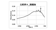
- FIG. 8 shows the composite copper foils of Example 3 and Comparative Example 3 after thermal compression bonding to the resin base material (CT-Z) and peeling, and then the surfaces of the composite copper foils were measured by the FT-IR/ATR method. This is the result.
- FIG. 9 is a secondary electron image and an EDS image of Cu obtained by analyzing the surface of the resin base material with a field emission scanning electron microscope after the composite copper foil was thermally compressed to and peeled off from the resin base material.
- FIG. 9 is a secondary electron image and an EDS image of Cu obtained by analyzing the surface of the resin base material with a field emission scanning electron microscope after the composite copper foil was thermally compressed to and peeled off from the resin base material.
- FIG. 10 shows the cross section of the seed layer formed on the resin substrate after the composite copper foils of Examples 1, 2 and 3 and Comparative Examples 3 and 7 were thermally compressed and peeled off from the resin substrate.
- FIG. 11 shows SEM images (magnification: 30,000) of cross sections of resins having seed layers of Examples 1, 2, and 3 and Comparative Example 7 that were plated.
- One embodiment of the disclosure of the present specification is a method for manufacturing a laminate of an insulating base layer and a copper member, comprising a step of bonding an insulating base layer and a copper member having protrusions on the surface; forming a seed layer by peeling off the member to transfer the projections to the surface of the insulating base layer; forming a resist on a predetermined location on the surface of the seed layer; a method of manufacturing comprising the steps of depositing copper by copper plating the areas where the resist is not deposited, removing the resist, and removing the seed layer exposed by the removal of the resist. be.
- the seed layer refers to the surface of the peeled copper member and the surface configured to include the bottom of the recesses formed in the insulating base layer by the protrusions of the copper member. Refers to the layer formed in between (FIG. 1B), so that the recess and the metal from the copper member transferred to the recess are contained within that layer.
- the bottom of the recess refers to the farthest bottom from the surface of the stripped copper member among the bottoms of the plurality of recesses, and the surface configured to include the bottom of the recess is the surface of the stripped copper member. parallel to the surface.
- Step of bonding an insulating base layer and a copper member ⁇ copper member> The surface of the copper member has fine protrusions.
- the arithmetic mean roughness (Ra) of the surface of the copper member is preferably 0.03 ⁇ m or more, more preferably 0.05 ⁇ m or more, and is preferably 0.3 ⁇ m or less, more preferably 0.2 ⁇ m or less. .
- the maximum height roughness (Rz) of the surface of the copper member is preferably 0.2 ⁇ m or more, more preferably 1.0 ⁇ m or more, and is preferably 2.0 ⁇ m or less, more preferably 1.7 ⁇ m or less. preferable.
- Ra and Rz are too small, the adhesion to the resin substrate will be insufficient, and if they are too large, fine wiring formability and high frequency characteristics will be inferior.
- Ra and Rz can be calculated by the method specified in JIS B 0601:2001 (in accordance with the international standard ISO4287-1997).
- the average length (RSm) of the surface roughness curve element of the copper member is not particularly limited, but is 1500 nm or less, 1400 nm or less, 1300 nm or less, 1200 nm or less, 1100 nm or less, 1000 nm or less, 900 nm or less, 800 nm or less, 750 nm or less, It is preferably 700 nm or less, 650 nm or less, 600 nm or less, 550 nm or less, 450 nm or less, or 350 nm or less, and preferably 100 nm or more, 200 nm or more, or 300 nm or more.
- RSm represents the average length of unevenness for one cycle included in the roughness curve at a certain reference length (lr) (that is, the length of the contour curve element: Xs1 to Xsm), It is calculated by the following formula.
- RSm can be measured and calculated according to "Method for measuring surface roughness of fine ceramic thin film by atomic force microscope (JIS R 1683:2007)".
- a layer containing copper oxide is formed on at least a part of the surface of the copper member.
- the copper member specifically includes, but is not limited to, copper foils such as electrolytic copper foil, rolled copper foil, and copper foil with a carrier, copper wires, copper plates, and copper lead frames.
- the copper member contains Cu as a main component, which is part of the structure, but a material made of pure copper with a Cu purity of 99.9% by mass or more is preferable, and is made of tough pitch copper, deoxidized copper, or oxygen-free copper. More preferably, it is made of oxygen-free copper with an oxygen content of 0.001% by mass to 0.0005% by mass.
- the copper member is a copper foil
- its thickness is not particularly limited, but is preferably 0.1 ⁇ m or more and 100 ⁇ m or less, more preferably 0.5 ⁇ m or more and 50 ⁇ m or less.
- the layer containing copper oxide is formed on the surface of the copper member and contains copper oxide (CuO) and/or cuprous oxide (Cu 2 O).
- This layer containing copper oxide can be formed by oxidizing the surface of the copper member. This oxidation treatment roughens the surface of the copper member.
- a surface roughening treatment step such as soft etching or etching is not necessary, but may be performed.
- degreasing treatment acid cleaning for uniformizing the surface by removing a natural oxide film, or alkali treatment for preventing acid from being brought into the oxidation process may be performed after acid cleaning.
- the method of alkali treatment is not particularly limited, but preferably 0.1 to 10 g/L, more preferably 1 to 2 g/L alkaline aqueous solution, such as sodium hydroxide aqueous solution, at 30 to 50 ° C. for 0.5 to 2 minutes. It should be treated to some extent.
- the oxidizing agent is not particularly limited, and for example, an aqueous solution of sodium chlorite, sodium hypochlorite, potassium chlorate, potassium perchlorate, etc. can be used.
- Various additives eg, phosphates such as trisodium phosphate dodecahydrate
- surface active molecules may be added to the oxidizing agent.
- Surface active molecules include porphyrins, porphyrin macrocycles, extended porphyrins, ring contracted porphyrins, linear porphyrin polymers, porphyrin sandwich coordination complexes, porphyrin sequences, silanes, tetraorgano-silanes, aminoethyl-aminopropyltrimethoxysilane, (3-aminopropyl)trimethoxysilane, (1-[3-(trimethoxysilyl)propyl]urea) ((l-[3-(Trimethoxysilyl)propyl]urea)), (3-aminopropyl)triethoxysilane , ((3-glycidyloxypropyl)trimethoxysilane), (3-chloropropyl)trimethoxysilane, (3-glycidyloxypropyl)trimethoxysilane, dimethyldichlorosilane, 3-(trimethoxysilyl)
- the protrusions on the surface of the oxidized copper member may be adjusted using a dissolving agent.
- the dissolving agent used in this dissolving step is not particularly limited, but is preferably a chelating agent, particularly a biodegradable chelating agent, such as ethylenediaminetetraacetic acid, diethanolglycine, tetrasodium L-glutamic acid diacetate, ethylenediamine-N,N'.
- the pH of the solution for dissolution is not particularly limited, but it is preferably alkaline, more preferably pH 8 to 10.5, still more preferably pH 9.0 to 10.5, and pH 9.8 to 10.5. 2 is more preferred.
- the surface of the layer containing copper oxide may be subjected to reduction treatment with a reducing agent, in which case cuprous oxide may be formed on the surface of the layer containing copper oxide.
- a reducing agent in which case cuprous oxide may be formed on the surface of the layer containing copper oxide.
- the reducing agent used in this reduction step include dimethylamine borane (DMAB), diborane, sodium borohydride, hydrazine and the like.
- Pure copper has a specific resistance of 1.7 ⁇ 10 -8 ( ⁇ m), while copper oxide has a specific resistance of 1 to 10 ( ⁇ m).
- Cuprous oxide is 1 ⁇ 10 6 to 1 ⁇ 10 7 ( ⁇ m), so the layer containing copper oxide has low conductivity. At most, transmission loss due to the skin effect is less likely to occur when forming a circuit of a printed wiring board or a semiconductor package substrate using the copper member according to the present invention.
- the layer containing copper oxide may contain a metal other than copper.
- the contained metal is not particularly limited, but contains at least one metal selected from the group consisting of Sn, Ag, Zn, Al, Ti, Bi, Cr, Fe, Co, Ni, Pd, Au and Pt. good too.
- metals having higher acid resistance and heat resistance than copper such as Ni, Pd, Au and Pt.
- a layer containing a metal other than copper may be formed on the layer containing copper oxide.
- This layer can be formed on the outermost surface of the copper member by plating.
- the plating method is not particularly limited. Plating can be performed by electrolytic plating, electroless plating, vacuum deposition, chemical conversion treatment, or the like, but electrolytic plating is preferred because it is preferable to form a uniform and thin plating layer.
- nickel plating and nickel alloy plating are preferable.
- Metals formed by nickel plating and nickel alloy plating include, for example, pure nickel, Ni—Cu alloy, Ni—Cr alloy, Ni—Co alloy, Ni—Zn alloy, Ni—Mn alloy, Ni—Pb alloy, Ni— P alloy etc. are mentioned.
- metal salts used for plating include nickel sulfate, nickel sulfamate, nickel chloride, nickel bromide, zinc oxide, zinc chloride, diamminedichloropalladium, iron sulfate, iron chloride, chromic anhydride, chromium chloride, sodium chromium sulfate, copper sulfate, copper pyrophosphate, cobalt sulfate, manganese sulfate, and the like;
- the bath composition is, for example, nickel sulfate (100 g/L or more and 350 g/L or less), nickel sulfamate (100 g/L or more and 600 g/L or less), nickel chloride (0 g/L or more and 300 g/L or less). and mixtures thereof are preferred, but sodium citrate (0 g/L or more and 100 g/L or less) or boric acid (0 g/L or more and 60 g/L or less) may be contained as additives.
- the copper oxide on the surface is first reduced, and an electric charge is used to turn it into cuprous oxide or pure copper. After that, the metal that forms the metal layer begins to deposit.
- the amount of charge varies depending on the type of plating solution and the amount of copper oxide. For example, when Ni plating is applied to a copper member, 10 C per area dm 2 of the copper member to be electrolytically plated is required to keep the thickness within a preferable range. It is preferable to apply an electric charge of 90C or more, and it is more preferable to apply an electric charge of 20C or more and 65C or less.
- the amount of metal deposited on the outermost surface of the copper member by plating is not particularly limited, it is preferably 0.8 to 6.0 mg/dm 2 .
- the amount of adhered metal can be calculated by, for example, dissolving in an acidic solution, measuring the amount of metal by ICP analysis, and dividing the amount by the plane visual field area of the structure.
- the surface of the copper member is partially coated with a coating agent such as a silane coupling agent or an antiseptic before the oxidation treatment; Steps such as treating the oxide-containing layer with a dissolving agent may be performed.
- a coating agent such as a silane coupling agent or a preservative
- the portion is prevented from being subjected to oxidation treatment, and voids are generated in the layer containing copper oxide, and the copper is removed from the copper member.
- Layers containing oxides tend to break.
- the dissolving agent is an agent that dissolves copper oxide, and by treating with the dissolving agent, the copper oxide near the interface between the copper member and the layer containing copper oxide is partially dissolved, The layer containing copper oxide is likely to break from the copper member.
- Silane coupling agents are not particularly limited, but silane, tetraorgano-silane, aminoethyl-aminopropyltrimethoxysilane, (3-aminopropyl)trimethoxysilane, (1-[3-(trimethoxysilyl)propyl]urea ) ((l-[3-(Trimethoxysilyl)propyl]urea)), (3-aminopropyl)triethoxysilane, ((3-glycidyloxypropyl)trimethoxysilane), (3-chloropropyl)trimethoxysilane, (3-glycidyloxypropyl)trimethoxysilane, dimethyldichlorosilane, 3-(trimethoxysilyl)propyl methacrylate, ethyltriacetoxysilane, triethoxy(isobutyl)silane, triethoxy(octyl)silane
- Rust inhibitors are not particularly limited, but 1H-tetrazole, 5-methyl-1H-tetrazole, 5-amino-1H-tetrazole, 5-phenyl-1H-tetrazole, 1,2,3-triazole, 1,2,4 -triazole, 1,2,3-benzotriazole, 5-methyl-1H-benzotriazole, 5-amino-1H-benzotriazole, 2-mercaptobenzothiazole, 1,3-dimethyl-5-pyrazolone, pyrrole, 3- methylpyrrole, 2,4-dimethylpyrrole, 2-ethylpyrrole, pyrazole, 3-aminopyrazole, 4-methylpyrazole, 3-amino-5-hydroxypyrazole, thiazole, 2-aminothiazole, 2-methylthiazole, 2- amino-5-methylthiazole, 2-ethylthiazole, benzothiazole, imidazole, 2-methylimidazole, 2-ethylimid
- the treatment with a silane coupling agent or antiseptic may be performed at any time before the oxidation treatment, such as degreasing, acid cleaning for uniform treatment by removing the native oxide film, or acid to the oxidation process after acid cleaning.
- the dissolving agent for making it easier to break the layer containing copper oxide from the copper member is not limited to Ni chloride, as long as it contains a component that dissolves copper oxide, and chlorides (potassium chloride, zinc chloride , iron chloride, chromium chloride, etc.), ammonium salts (ammonium citrate, ammonium chloride, ammonium sulfate, nickel ammonium sulfate, etc.), chelating agents (ethylenediaminetetraacetic acid, diethanolglycine, L-glutamic acid diacetic acid/tetrasodium, ethylenediamine-N, N'-disuccinic acid, sodium 3-hydroxy-2,2'-iminodisuccinate, trisodium methylglycine diacetate, tetrasodium aspartate diacetate, disodium N-(2-hydroxyethyl)iminodiacetate, sodium gluconate etc.), tin(II) chloride, and citric acid.
- the copper member on which the layer containing copper oxide is formed is immersed in a Ni chloride solution (concentration of 45 g/L or more) at room temperature or at a temperature higher than room temperature for 5 seconds or more. is preferred.
- a Ni chloride solution concentration of 45 g/L or more
- treatment may be performed simultaneously with oxidation treatment, or treatment may be performed simultaneously with plating treatment after oxidation treatment.
- Ni chloride is contained in the plating solution, and a layer containing copper oxide is formed in the plating solution for 5 seconds, 10 seconds, 15 seconds, 20 seconds, 30 seconds, 1 minute, or 2 minutes before plating.
- the formed copper member may be immersed.
- the immersion time can be appropriately changed depending on the oxide film thickness.
- the base material of the insulating base material layer should be such that when the surface of the copper member on which the unevenness is formed is bonded to the insulating base material layer, the surface profile including the uneven shape of the copper member is transferred to the resin base material.
- a resin substrate is preferable.
- the resin base material is a material containing resin as a main component, but the type of resin is not particularly limited, and may be a thermoplastic resin or a thermosetting resin, polyphenylene ether (PPE), Epoxy, polyphenylene oxide (PPO), polybenzoxazole (PBO), polytetrafluoroethylene (PTFE), liquid crystal polymer (LCP), thermoplastic polyimide (TPI), fluororesin, polyetherimide, polyetheretherketone, polycyclo Olefins, bismaleimide resins, low dielectric constant polyimides, cyanate resins, or mixed resins thereof can be exemplified.
- the resin base material may further contain an inorganic filler or glass fiber.
- the dielectric constant of the insulating substrate layer used is preferably 5.0 or less, more preferably 4.0 or less, and even more preferably 3.8 or less.
- the bonding method is not particularly limited, but thermal press fitting is preferred.
- the resin base material and the copper member may be adhered and laminated, and then heat treated under predetermined conditions.
- predetermined conditions eg, temperature, pressure, time, etc.
- Predetermined conditions include, for example, the following conditions.
- a copper member is heated to the resin base material by applying a pressure of 0 to 20 MPa at a temperature of 50 ° C. to 300 ° C. for 1 minute to 5 hours. Crimping is preferred.
- the resin substrate is GX13 (manufactured by Ajinomoto Fine-Techno Co., Ltd.), it is heated while being pressurized at 1.0 MPa and held at 180° C. for 60 minutes for thermocompression bonding.
- the resin base material contains or consists of a PPE resin
- a copper member is attached to the resin base material by applying a pressure of 0 to 20 MPa at a temperature of 50° C. to 350° C. for 1 minute to 5 hours. Thermocompression bonding is preferred.
- the resin substrate is R5620 (manufactured by Panasonic)
- the temperature and pressure are increased to 2.0 to 3.0 MPa after thermocompression bonding while heating to 100 ° C. under a pressure of 0.5 MPa. , 200 to 210° C. for 120 minutes for further thermocompression bonding.
- the temperature and pressure are increased to 3.0 to 4.0 MPa after thermocompression bonding while heating to 110 ° C. under a pressure of 0.5 MPa. , and 195° C. for 75 minutes for thermocompression bonding.
- the heat of the copper member is applied to the resin base material by applying a pressure of 0 to 20 MPa at a temperature of 50 ° C. to 400 ° C. for 1 minute to 5 hours. Crimping is preferred.
- a copper member is formed on the resin substrate by applying a pressure of 0 to 20 MPa at a temperature of 50 ° C. to 400 ° C. for 1 minute to 5 hours.
- Heat crimping is preferred.
- the resin substrate is CT-Z (manufactured by Kuraray)
- it is heated under a pressure of 0 MPa, held at 260 ° C. for 15 minutes, further heated while being pressurized at 4 MPa, and held at 300 ° C. for 10 minutes. heat press.
- Step of peeling off the copper member After the copper member is attached to the insulating base layer, when the copper member is peeled off from the insulating base layer under predetermined conditions, the protrusions on the surface of the copper member are removed from the insulating base layer. to form a seed layer on the surface of the insulating base layer. Therefore, the surface of the insulating base layer becomes flat.
- the thickness of the seed layer may be 2.50 ⁇ m or less, more preferably 2.00 ⁇ m or less, and even more preferably 1.70 ⁇ m or less. Moreover, it is preferably 0.01 ⁇ m or more, more preferably 0.10 ⁇ m or more, and even more preferably 0.36 ⁇ m or more. If the thickness is less than 0.01 ⁇ m, the plating formability is poor and the adhesion to the insulating substrate is lowered. If it exceeds 2.50 ⁇ m, the wiring formability is deteriorated.
- the method for measuring the thickness of the seed layer is not particularly limited, and for example, the thickness of the seed layer may be measured in the SEM image.
- the seed layer thus produced is used as it is as part of the circuit.
- the adhesion between the copper and the insulating base layer is improved.
- the conditions for peeling off the copper member from the insulating base layer are not particularly limited, but a 90° peeling test (Japanese Industrial Standards (JIS) C5016 "Flexible printed wiring board test method"; corresponding international standards IEC249-1: 1982, IEC326- 2:1990).
- the method of peeling off the copper member from the insulating base material layer is not particularly limited, but a machine may be used, or a manual operation may be performed.
- the metal transferred to the surface of the insulating substrate layer after peeling off the copper member can be analyzed by various methods (e.g., X-ray photoelectron spectroscopy (XPS), energy dispersive X-ray spectroscopy (EDS), ICP emission spectroscopy). (Inductively Coupled Plasma Emission Spectroscopy, ICP-OES/ICP-AES)).
- XPS X-ray photoelectron spectroscopy
- EDS energy dispersive X-ray spectroscopy
- ICP emission spectroscopy ICP emission spectroscopy
- ICP-OES/ICP-AES Inductively Coupled Plasma Emission Spectroscopy
- XPS is a technique for performing energy analysis by irradiating an object with X-rays and capturing photoelectrons e ⁇ emitted as the object is ionized.
- XPS it is possible to examine the types, abundances, chemical bonding states, etc. of elements present on the surface of the sample or from the surface to a predetermined depth (for example, up to a depth of 6 nm).
- the diameter of the analysis spot (that is, the diameter of the cross section of the cylindrical portion that can be analyzed so that the cross section is circular) is suitably 1 ⁇ m or more and 1 mm or less.
- the metal atoms contained in the layer containing copper oxide may be detected from the surface of the insulating base material from which the copper member has been peeled off by XPS Survey spectrum analysis.
- the metal contained in the convex part of the copper member is insulated so as to fill 70% or more, 80% or more, 90% or more, 95% or more, 99% or more, or 99.9% or more of the concave part of the transferred surface profile. Transfer to the substrate layer is preferred.
- the metal fills most of the recesses in the insulating base layer, when the surface of the insulating base layer is measured by XPS, the total peak intensity of the main peaks of the spectrum of metal atoms is higher than the peak intensity of the main peak of the spectrum of C1s. will also grow.
- the main peak is the peak with the highest intensity among multiple peaks of the metal element.
- Cu is 2p3 orbital
- Sn is 3d5 orbital
- Ag is 3d5 orbital
- Zn is 2p3 orbital
- Al is 2p orbital
- Ti is 2p3 orbital
- Bi is 4f7 orbital
- Cr is 2p3 orbital
- Fe is 2p3 orbital
- Co is 2p3
- the main peak is the 2p3 orbital of Ni, the 3d5 orbital of Pd, the 4f7 orbital of Au, and the 4f7 orbital of Pt.
- the peak intensity of the spectrum referred to here means the height in the vertical axis direction of the XPS spectrum data.
- the ratio of Cu2p3 to the total atoms on the surface of the insulating base layer from which the copper member is peeled off, as measured by XPS, is 1.0 atom% or more, 1.8 atom% or more, 2.8 atom% or more, 3.0 atom% or more, It is preferably 4.0 atom % or more, 5.0 atom % or more, or 6.0 atom %.
- the ratio of the surface atomic composition percentage of Cu2p3 / the surface atomic composition percentage of C1s is 0.010 or more, 0.015 or more, 0.020 or more, 0 It is preferably 0.025 or more, 0.030 or more, 0.035 or more, 0.040 or more, 0.045 or more, 0.050 or more, or 0.10 or more.
- the total atomic composition percentage of the metal atoms on the surface of the peeled insulating base layer measured by X-ray photoelectron spectroscopy (XPS) is 1.0 atom. % or more, 1.5 atom % or more, 1.8 atom % or more, 2.8 atom % or more, 3.0 atom % or more, 4.0 atom % or more, 5.0 atom % or more, or 6.0 atom %.
- the value of the ratio of (total atomic composition percentage of metal atoms on the surface of the peeled insulating base layer):(atomic composition percentage of C1s on the surface of the peeled insulating base layer) is 0.010. 0.015 or more, 0.020 or more, 0.025 or more, 0.030 or more, 0.035 or more, 0.040 or more, 0.045 or more, 0.050 or more, or 0.10 or more preferable.
- the ratio of Cu should be 1 atom% or more, preferably 4 atom% or more, and 7 atom% or more. It is more preferably 10 atom % or more, further preferably 11.4 atom % or more.
- the transfer efficiency indicates the rate at which the metal contained in the protrusions formed on the copper member is transferred to the insulating base layer.
- composition ratio of the sum of the metals on the surface of the insulating base layer from which the copper member has been peeled off/(C+O) measured by EDS may be 0.38 or more, preferably 0.40 or more. , is more preferably 0.42 or more, and more preferably 0.43 or more.
- the amount of substances derived from the insulating base layer detected from the surface of the copper member peeled off from the insulating base layer is preferably below the detection limit or, if detected, is a small amount. This is because, in that case, when the copper member is peeled off, breakage in the insulating base material layer can be sufficiently suppressed.
- the method for detecting substances derived from the insulating base layer is not particularly limited, and a method suitable for the target substance may be used. For example, in the case of organic substances, attenuated total reflection absorption Fourier transform infrared spectroscopy (FT-IR method) ("Infrared and Raman Spectroscopy: Principles and Spectral Interpretation" by Peter Larkin).
- the FT - IR method is an infrared spectroscopic method in which the substance to be measured is irradiated with infrared rays, and the compound is identified and / or quantified using the infrared absorption spectrum.
- the N ratio is preferably 10 or less and 9 or less, more preferably 8 or less and 7 or less, and preferably no peak derived from the resin substrate is detected.
- the ratio of Ra after peeling to Ra before bonding on the surface of the copper member on which the layer having the protrusions is formed is less than 100%, less than 96%, less than 95%, less than 94%, less than 93%, and 92%. preferably less than, less than 91%, less than 90%, less than 80%, less than 70%, less than 65% or less than 60%.
- a smaller ratio means that the metal forming the layer having protrusions transferred to the insulating base layer.
- the ratio of the surface area after peeling to the surface area before bonding of the copper member on which the layer having the convex portion is formed is less than 100%, less than 98%, less than 97%, less than 96%, less than 95%, less than 94%. , less than 93%, less than 92%, less than 91%, less than 90%, less than 80% or less than 75%.
- a smaller ratio means that the metal forming the layer having protrusions transferred to the insulating base layer.
- the surface area can be measured using a confocal microscope or an atomic force microscope.
- ⁇ E * ab between the surface of the copper member before thermocompression bonding and the surface of the copper member after peeling is 13 or more, 15 or more, 20 or more, 25 or more, 30 or more, or 35 or more. It means that the larger the difference, the more the metal forming the protrusions transferred to the insulating base layer.
- the adhesiveness between the resin substrate and the seed layer is enhanced by forming irregularities that serve as anchors in the resin.
- relatively large unevenness was formed on the surface to ensure adhesion, but this caused copper to precipitate deep from the resin surface layer, so when the seed layer was etched and removed, a small amount of copper remained. tended to A deep etching process was necessary because this trace amount of remaining copper could cause a short circuit between wirings.
- the effect of increasing adhesion by unevenness forming treatment and electroless copper plating film is that selectivity to resin substrates is high, and sufficient adhesion effect can be obtained only in some cases such as ABF (Ajinomoto Build-Up Film). It is only a resin base material.
- an ultra-thin copper foil with a carrier is used, but the thickness of the ultra-thin copper foil layer must be 1.5 ⁇ m or more from the viewpoint of handling, etc.
- roughening treatment of 1 ⁇ m or more is performed. ing.
- the adhesion between the resin substrate and the seed layer is enhanced.
- a deep etching process was required.
- the seed layer obtained by the method of the present disclosure has a smaller surface roughness than the case where the surface is roughened by desmear treatment in the conventional SAP method or the case where the ultra-thin copper foil with a carrier is roughened in the conventional MSAP method. Also, it is possible to avoid problems such as residual copper after etching, pattern skipping due to side etching in fine patterns, and transmission loss of high-frequency signals due to unevenness. In addition, although the surface roughness is small, fine unevenness is densely present, so that the insulating base material and copper are sufficiently adhered to each other.
- the resist may contain, for example, a material that is cured or dissolved by exposure to light, and is not particularly limited, but is preferably formed of a dry film resist (DFR), a positive liquid resist, or a negative liquid resist.
- DFR dry film resist
- DFR preferably contains a binder polymer that contributes to film formability, a monomer that undergoes a photopolymerization reaction upon UV irradiation (for example, an acrylic ester-based or methacrylic ester-based monomer), and a photopolymerization initiator.
- a dry film having a three-layer structure of cover form/photoresist/carrier film is preferably used for forming the DFR.
- a DFR, which is a resist can be formed on the structure by laminating the photoresist on the structure while peeling off the cover film, and then peeling off the carrier film after the lamination.
- Liquid resists include novolak resins that are soluble in organic solvents.
- the resist can be formed by coating the surface of the structure, drying it, and then dissolving or curing the resist by light irradiation.
- the thickness of the resist is not particularly limited, it is preferably 1 ⁇ m to 200 ⁇ m.
- the surface of the seed layer may be plated to form a second seed layer.
- the method of plating treatment is not particularly limited, and may be electrolytic plating or electroless plating.
- a film may be formed by a plating method.
- the second seed layer refers to a metal thin film formed by plating.
- the thickness of the second seed layer is not particularly limited, and may be about 0.02 to 2 ⁇ m. .
- the method of copper plating treatment is not particularly limited, and plating treatment can be performed using a known method.
- the method of removing the resist is not particularly limited, and known methods such as a method using fuming nitric acid or sulfuric acid-hydrogen peroxide mixture, and a dry ashing method using O 2 plasma or the like can be used.
- Step of Removing Seed Layer The method for removing the seed layer is not particularly limited, and known methods such as quick etching and flash etching using a sulfuric acid-hydrogen peroxide-based etchant can be used.
- One embodiment of the present invention is a method for selecting a copper member having a layer containing copper oxide formed on at least part of the surface thereof, wherein the copper member is thermally compressed to a resin base material and then pulled from the resin base material.
- a step of peeling a step of analyzing the surface of the copper member peeled off from the resin base material by attenuated total reflection absorption Fourier transform infrared spectroscopy (FT-IR / ATR method), and a resin base material with the copper member peeled off.
- FT-IR / ATR method attenuated total reflection absorption Fourier transform infrared spectroscopy
- a step of performing EDS elemental analysis on the surface of the copper member a step of measuring the thickness of the seed layer formed on the resin base material from which the copper member is peeled off, and a copper member obtained by the FT-IR / ATR method.
- the S/N ratio of the peak corresponding to the substance derived from the resin substrate on the surface is 10 or less in the wavelength range 700-4000 cm -1 , and the total metal on the surface of the copper member obtained by EDS elemental analysis / ( C+O) composition ratio is 0.4 or more, and the thickness of the seed layer is 0.1 ⁇ m or more and 2.0 ⁇ m or less, selecting a copper member.
- Another embodiment of the present invention is a method for selecting a copper member having a layer containing copper oxide formed on at least part of the surface thereof, wherein the copper member is thermally compressed to a resin base material, and then A step of peeling off, a step of performing Survey spectrum analysis of X-ray photoelectron spectroscopy (XPS) on the surface of the copper member peeled off from the resin substrate, and a surface of the resin substrate from which the copper member was peeled off , a step of performing EDS elemental analysis, a step of measuring the thickness of the seed layer formed on the resin base material from which the copper member has been peeled off, and The composition ratio of total metal on the surface of the copper member/(C+O) detected from the surface of the peeled resin base material and obtained by EDS elemental analysis is 0.4 or more, and the thickness of the seed layer is 0.4. selecting a copper member having a thickness of 1 ⁇ m or more and 2.0 ⁇ m or less.
- XPS X-ray photoelectron
- Each step can be performed according to the details described in the manufacturing method of the laminate.
- this selection method it is possible to select a copper member having good plating and wiring forming properties when a circuit is formed.
- Comparative Example 7 an ultra-thin copper foil with a carrier (MT18FL, ultra-thin copper foil thickness: 1.5 ⁇ m) manufactured by Mitsui Mining & Smelting Co., Ltd. was used as it was. In addition, Comparative Example 1 does not use a composite copper foil as described later.
- MT18FL ultra-thin copper foil thickness: 1.5 ⁇ m
- Example 1 potassium carbonate 2.5 g / L; KBE-903 (3-aminopropyltriethoxysilane; manufactured by Shin-Etsu Silicone Co., Ltd.) 1 vol%
- Example 3 contains 2.5 g/L of potassium carbonate; 0.06 g/L of potassium bicarbonate;
- Examples 4 to 6 contain 5 g/L of potassium hydroxide
- Comparative Example 2 is a solution of 2.5 g/L of potassium carbonate
- Comparative Example 3 is a solution of potassium carbonate 2.5 g / L; potassium hydrogen carbonate 0.06 g / L;
- Comparative Example 5 is potassium hydroxide 5 g / L; KBM-603 (N-2-(aminoethyl)-3 -Aminopropyltrimethoxysilane; manufactured by Shin-Etsu Silicone Co., Ltd.) 5 vol%
- Comparative Example 6 contains potassium hydroxide
- Comparative Example 3 contains sodium chlorite 58.8 g/L as an oxidizing agent; potassium hydroxide 8.8 g/L; potassium carbonate 3 g/L; KBM-403 (3-glycidoxypropyltrimethoxysilane; Shin-Etsu Silicone Co., Ltd.) 2 g/L solution was used.
- Examples 1 and 2 and Comparative Examples 5 and 6 were immersed in the oxidizing agent at 73° C. for 6 minutes, and Examples 3 to 6 and Comparative Examples 2 and 3 were immersed in the oxidizing agent at 73° C. for 2 minutes.
- Example 4 was treated at 45° C. for 10 seconds using a solution of 45 g/L of tin(II) chloride dihydrate and 1 mL/L of hydrochloric acid.
- Example 5 was treated at 45° C. for 60 seconds using a solution of 45 g/L of ammonium chloride.
- Example 6 was treated at 45° C. for 60 seconds using a 50% citric acid solution of 45 mL/L.
- a laminate sample was obtained by laminating prepreg on a test piece and thermocompression bonding in a vacuum using a vacuum high pressure press.
- the resin base material is R5670KJ (manufactured by Panasonic)
- the temperature and pressure are increased to 2.94 MPa and 210° C. for 120 minutes after thermocompression bonding while heating to 110° C. under a pressure of 0.49 MPa. It was thermocompression bonded by holding.
- the resin base material is R5680J (manufactured by Panasonic) after heat-pressing while heating to 110 ° C. under a pressure of 0.5 MPa, the temperature and pressure are increased, and held for 75 minutes at 3.5 MPa and 195 ° C. It was thermocompression bonded by doing.
- the resin substrate is NX9255 (manufactured by Park Electrochemical)
- it is heated to 260°C while pressurizing at 0.69 MPa, and the pressure is increased to 1.5 MPa and heated to 385°C. It was thermocompression bonded by holding for 1 minute.
- the resin substrate is R1551GG (manufactured by Panasonic)
- it is heated under a pressure of 1 MPa, and after reaching 100 ° C., it is held at that temperature for 10 minutes, and then further heated under a pressure of 3.3 MPa to 180 ° C. After the temperature was reached, the temperature was maintained for 50 minutes for thermocompression bonding.
- the resin substrate is CT-Z (manufactured by Kuraray Co., Ltd.), it is heated under a pressure of 0 MPa, held at 260° C. for 15 minutes, further heated while being pressurized at 4 MPa, and held at 300° C. for 10 minutes. crimped.
- the copper member was peeled off from the resin substrate according to the 90° peeling test (Japanese Industrial Standards (JIS) C5016) for these laminate samples (Fig. 1). Visual observation results are shown in Figure 2-1. Photographs of the surfaces of the resin side and the copper foil side after peeling off are shown in Fig. 2-2 for representative combinations.
- Example 1 since the composite copper foil was not plated, only Cu atoms were transferred and detected on the resin substrate side. In Examples 2 and 3, since Ni plating was performed, Cu atoms and Ni atoms were transferred and detected on the resin side.
- the ratio of C1s was smaller in both Examples and Comparative Examples 5 and 6 than in Comparative Examples 1 to 4. In the examples, it is believed that the proportion of C1s on the surface was relatively decreased due to the transfer of cupric oxide or cuprous oxide.
- R1551GG When using R1551GG as a resin base material, it is around 1200 cm -1 , when using R5670KJ and R5680J, it is around 1190 cm -1 , when using NX9255, it is around 1232 cm -1, and when CT - Z is used, it is 1741 cm -1 .
- the maximum peak detectable wavelength was taken to be around 1 (the arrows in FIGS. 4 to 8 indicate the maximum peak detectable wavelength).
- the S/N ratio was calculated using the noise value (N) as the difference between the maximum and minimum values of the peaks detected at a wavelength of 3800-3850 cm ⁇ 1 .
- Elemental Analysis by EDS (Energy Dispersive X-ray Spectrometer)> First, elemental analysis was performed using an EDS (energy dispersive X-ray spectroscope) (manufactured by Oxford, trade name: X-Max Extreme) (conditions: acceleration voltage of 10 kV, magnification of 30,000 times).
- FIG. 9 shows a typical secondary electron image and an EDS elemental mapping image of Cu
- Table 6 (Example) and Table 7 (Comparative Example) show the ratio of each element of C, O, Ni, Cu, and Sn ( atom %), and the value of the ratio (sum of ratios of metal elements/(sum of ratios of C and O)) calculated from these values.
- the ratio of Cu is 10 atom % or more, and Cu transfers at a high ratio, and (the sum of the ratios of metal elements/(the sum of the ratios of C and O)) is 0.4 or more. , good plating formability.
- the proportion of Cu was 0.1 atom % or less, and almost no Cu was transferred, resulting in poor plating formability.
- Comparative Examples 5 and 6 (the sum of the proportions of the metal elements/(the sum of the proportions of C and O)) is as low as less than 0.4, and these are also poor in plating formability.
- the resin having a seed layer produced using the composite copper foil of the example has good plating formability in terms of surface element composition.
- Seed layer thickness The thickness of the seed layer was then measured. Specifically, in the cross section of SEM (magnification: 10,000 times), for the layer in which the copper protrusions are embedded in the resin base material, the upper side corresponding to the upper surface of the layer and the lower side corresponding to the lower surface of the layer are in contact with each other. The maximum distance between two parallel straight lines was examined, and the distance was taken as the thickness of the seed layer.
- FIG. 10 shows a representative SEM image, and Tables 6 and 7 show the thickness measurement results.
- the wiring formability is good.
- Comparative Examples 2 and 3 since the thickness of the seed layer was 0 ⁇ m and metal transfer did not occur, almost no plating was formed.
- Comparative Example 7 since the seed layer is too thick, it is difficult to miniaturize the circuit, and the wiring formability is also poor as shown in ⁇ 3> below.
- the resin having a seed layer produced using the composite copper foil of the example has good wiring formability in terms of the thickness of the seed layer.
- electrolytic copper plating was performed at a current density of 1 A/dm 2 at 30° C. for 30 minutes to form an electrolytic copper plating film with a thickness of 15 ⁇ m.
- the seed layer under the plating resist was dissolved and removed by etching using a mixed solution of sulfuric acid and hydrogen peroxide to obtain a laminated wiring circuit board.
- the resin having the seed layer of Example 3 was subjected to electroplating alone to form a second seed layer. Specifically, using a commercially available electrolytic copper plating solution, an electrolytic copper plating film was formed at a current density of 1 A/dm 2 at 30°C.
- FIG. 11 shows SEM cross-sectional images (30000 times) of Examples 1, 2 and 3 and Comparative Example 7.
- electrolytic copper plating was performed at a current density of 1 A/dm 2 at 30° C. for 30 minutes to form an electrolytic copper plating film with a thickness of 15 ⁇ m.
- the seed layer under the plating resist was dissolved and removed by etching using a mixed solution of sulfuric acid and hydrogen peroxide to obtain a laminated wiring circuit board.
- Comparative Example 7 has a low etching factor and poor wiring formability.
Abstract
Description
前記銅部材を、樹脂基材に熱圧着した後に前記樹脂基材から引き剥がした時、
減衰全反射吸収フーリエ変換赤外分光法(FT-IR/ATR法)によって得られる、前記銅部材の表面における、樹脂基材由来の物質に対応するピークのS/N比が、波長範囲700-4000cm-1において10以下であり、
EDS元素分析によって得られる、前記樹脂基材の表面の金属の合計/(C+O)の組成割合が0.4以上であり、
前記樹脂基材において形成されるシード層の厚さが0.1μm以上、2.0μm以下である、銅部材。
[2] 前記ピークのS/N比が7以下である、[1]項に記載の銅部材。
[3] 銅部材の表面の少なくとも一部に銅酸化物を含む層が形成された銅部材であって、 前記銅部材を、樹脂基材に熱圧着した後に前記樹脂基材から引き剥がした時、
X線光電子分光法(XPS)のSurvey spectrum分析によって、前記銅酸化物を含む層に含まれる金属原子が、前記銅部材が引き剥がされた前記樹脂基材の表面から検出され、
EDS元素分析によって得られる、前記樹脂基材の表面の金属の合計/(C+O)の組成割合が0.4以上であり、
前記樹脂基材において形成されるシード層の厚さが0.1μm以上、2.0μm以下である、銅部材。
銅部材。
[4] 前記銅部材が引き剥がされた前記樹脂基材の表面から検出される金属元素のメインピークの強度の合計がC1sのピーク強度よりも大きい、[3]項に記載の銅部材。
[5] 前記銅部材が引き剥がされた前記樹脂基材の表面において、XPSによる測定結果から算出された
[金属元素の表面原子組成百分率(atom%)の合計]/[C1sの表面原子組成百分率(atom%)]
が0.010以上である、[4]項に記載の銅部材。
[6] 前記Survey spectrum分析によって検出されるCu2p3とNi2p3の表面原子組成百分率の合計が1.5atom%以上である、[4]項に記載の銅部材。
[7] 前記Survey spectrum分析によって検出されるCu2p3の表面原子組成百分率が1.0atom%以上である、[4]項に記載の銅部材。
[8] 前記銅酸化物を含む層が形成された表面のRaが0.04μm以上であって、前記Raに対する、前記樹脂基材から引き剥がされた前記銅部材の表面のRaの割合が100%未満である、[1]~[7]のいずれか一項に記載の銅部材。
[9] 前記銅酸化物を含む層が形成された表面の表面積に対する、前記樹脂基材から引き剥がされた前記銅部材の表面積の割合が100%未満である、[1]~[8]のいずれか一項に記載の銅部材。
[10] 前記銅酸化物を含む層が形成された表面と前記樹脂基材から引き剥がされた前記銅部材の表面の色差(ΔE*ab)が15以上である、[1]~[9]のいずれか一項に記載の銅部材。
[11] 前記樹脂基材は、ポリフェニレンエーテル(PPE)、エポキシ、ポリフェニレンオキシド(PPO)、ポリベンゾオキサゾール(PBO)、ポリテトラフルオロエチレン(PTFE)、液晶ポリマー(LCP)、または熱可塑性ポリイミド(TPI)、フッ素樹脂、ポリエーテルイミド、ポリエーテルエーテルケトン、ポリシクロオレフィン、ビスマレイミド樹脂、低誘電率ポリイミド及びシアネート樹脂からなる群から選択された少なくとも1つの絶縁性樹脂を含有する、[1]~[10]のいずれか一項に記載の銅部材。
[12] 前記銅部材が、前記樹脂基材に、50℃~400℃の温度、0~20MPaの圧力、1分~5時間の時間、の条件で熱圧着される、[1]~[11]のいずれか一項に記載の銅部材。
[13] 前記銅酸化物を含む層が銅以外の金属を含む、[1]~[12]のいずれか一項に記載の銅部材。
[14] 前記銅以外の金属がNiである、[13]項に記載の銅部材。
[15] 表面の少なくとも一部に銅酸化物を含む層が形成された銅部材の選択方法であって、
前記銅部材を、樹脂基材に熱圧着した後に前記樹脂基材から引き剥がす工程と、
前記樹脂基材から引き剥がされた前記銅部材の表面を減衰全反射吸収フーリエ変換赤外分光法(FT-IR/ATR法)で解析する工程と、
前記銅部材を引き剥がした前記樹脂基材の表面に対し、EDS元素分析を行う工程と、 前記銅部材を引き剥がした前記樹脂基材において形成されるシード層の厚さを測定する工程と、
前記FT-IR/ATR法によって得られる、前記銅部材の表面における、樹脂基材由来の物質に対応するピークのS/N比が、波長範囲700-4000cm-1において10以下であり、
前記EDS元素分析によって得られる、前記銅部材の表面の金属の合計/(C+O)の組成割合が0.4以上であり、
前記シード層の厚さが0.1μm以上、2.0μm以下である、銅部材を選択する工程と、
を含む選択方法。
[16] 表面の少なくとも一部に銅酸化物を含む層が形成された銅部材の選択方法であって、
前記銅部材を、樹脂基材に熱圧着した後に前記樹脂基材から引き剥がす工程と、
前記樹脂基材から引き剥がされた前記銅部材の表面に対し、X線光電子分光法(XPS)のSurvey spectrum分析を行う工程と、
前記銅部材を引き剥がした前記樹脂基材の表面に対し、EDS元素分析を行う工程と、 前記銅部材を引き剥がした前記樹脂基材において形成されるシード層の厚さを測定する工程と、
前記銅酸化物を含む層に含まれる金属原子が、前記銅部材が引き剥がされた前記樹脂基材の表面から検出され、
前記EDS元素分析によって得られる、前記銅部材の表面の金属の合計/(C+O)の組成割合が0.4以上であり、
前記シード層の厚さが0.1μm以上、2.0μm以下である、
銅部材を選択する工程と、
を含む選択方法。
[17] 前記銅部材の表面をシランカップリング剤または防錆剤で部分コートする工程と、
前記部分コートされた前記表面を酸化処理することにより前記銅酸化物を含む層を形成する工程と、
をさらに含む、[16]項の選択方法。
[18] 前記銅部材の前記表面が酸化剤によって酸化処理される、[17]項の選択方法。
[19] 前記シランカップリング剤が、シラン、テトラオルガノ-シラン、アミノエチル-アミノプロピルトリメトキシシラン、(3-アミノプロピル)トリメトキシシラン、(1-[3-(トリメトキシシリル)プロピル]ウレア)((l-[3-(Trimethoxysilyl)propyl]urea))、(3-アミノプロピル)トリエトキシシラン、((3-グリシジルオキシプロピル)トリメトキシシラン)、(3-クロロプロピル)トリメトキシシラン、(3-グリシジルオキシプロピル)トリメトキシシラン、ジメチルジクロロシラン、3-(トリメトキシシリル)プロピルメタクリレート、エチルトリアセトキシシラン、トリエトキシ(イソブチル)シラン、トリエトキシ(オクチル)シラン、トリス(2-メトキシエトキシ)(ビニル)シラン、クロロトリメチルシラン、メチルトリクロロシラン、四塩化ケイ素、テトラエトキシシラン、フェニルトリメトキシシラン、クロロトリエトキシシラン、エチレン-トリメトキシシランからなる群から選択される、[17]または[18]項に記載の選択方法。
[20] 前記防錆剤が、1H-テトラゾール、5-メチル-1H-テトラゾール、5-アミノ-1H-テトラゾール、5-フェニル-1H-テトラゾール、1,2,3-トリアゾール、1,2,4-トリアゾール、1,2,3-ベンゾトリアゾール、5-メチル-1H-ベンゾトリアゾール、5-アミノ-1H-ベンゾトリアゾール、2-メルカプトベンゾチアゾール、1,3-ジメチル-5-ピラゾロン、ピロール、3-メチルピロール、2,4-ジメチルピロール、2-エチルピロール、ピラゾール、3-アミノピラゾール、4-メチルピラゾール、3-アミノ-5-ヒドロキシピラゾール、チアゾール、2-アミノチアゾール、2-メチルチアゾール、2-アミノ-5-メチルチアゾール、2-エチルチアゾール、ベンゾチアゾール、イミダゾール、2-メチルイミダゾール、2-エチルイミダゾール、2-ブチルイミダゾール、5-アミノイミダゾール、6-アミノイミダゾール、ベンゾイミダゾール、2-(メチルチオ)ベンゾイミダゾールからなる群から選択される、[17]または[18]項に記載の選択方法。
[21] 前記酸化処理された前記表面に、銅以外の金属を含む層を形成する工程をさらに含む、[17]~[20]のいずれか一項に記載の選択方法。
[22] 前記銅以外の金属がNiである、[21]項に記載の選択方法。
[23] 前記銅部材の前記表面を酸化処理する工程と、
前記酸化処理された前記表面を溶解剤で処理することにより前記銅酸化物を含む層を形成する工程と、
をさらに含む、[16]項の選択方法。
[24] 前記銅部材の前記表面が酸化剤によって酸化処理される、[23]項の選択方法。
[25] 前記溶解剤が、塩化Ni、塩化亜鉛、塩化鉄、塩化クロム、クエン酸アンモニウム、塩化カリウム、硫酸アンモニウム、塩化アンモニウム、硫酸ニッケルアンモニウム、エチレンジアミン四酢酸、ジエタノールグリシン、L-グルタミン酸二酢酸・四ナトリウム、エチレンジアミン-N,N’-ジコハク酸、3-ヒドロキシ-2、2’-イミノジコハク酸ナトリウム、メチルグリシン2酢酸3ナトリウム、アスパラギン酸ジ酢酸4ナトリウム、N-(2-ヒドロキシエチル)イミノ二酢酸ジナトリウム、グルコン酸ナトリウム、塩化スズ(II)、及びクエン酸からなる群から選択される、[23]項に記載の選択方法。
[26] 前記溶解剤で処理された前記表面に、銅以外の金属を含む層を形成する工程をさらに有する、[23]~[25]のいずれか一項に記載の選択方法。
[27] 前記銅以外の金属がNiである、[26]項に記載の選択方法。
[28] [1]~[14]のいずれか一項に記載の銅部材の製造方法であって、
1)銅部材の前記表面をシランカップリング剤または防錆剤で部分コートする工程;及び
2)前記部分コートされた前記表面を酸化処理することにより前記銅酸化物を含む層を形成する工程;
を含む、銅部材の製造方法。
[29] [13]または[14]項に記載の銅部材の製造方法であって、
1)銅部材の前記表面をシランカップリング剤または防錆剤で部分コートする工程; 2)前記部分コートされた前記表面を酸化処理することにより前記銅酸化物を含む層を形成する工程;
3)酸化処理された前記表面に、銅以外の金属を含む層を形成する工程;
を含む、銅部材の製造方法。
[30] [1]~[14]のいずれか一項に記載の銅部材の製造方法であって、
1)前記部分コートされた前記表面を酸化処理することにより前記銅酸化物を含む層を形成する工程; および
2)前記酸化処理された前記表面を溶解剤で処理する工程
を含む、銅部材の製造方法。
[31] [13]または[14]項に記載の銅部材の製造方法であって、
1)前記銅部材の前記表面を酸化処理することにより前記銅酸化物を含む層を形成する工程;
2)前記酸化処理された前記表面を溶解剤で処理する工程;及び
3)前記溶解剤で処理された前記表面に銅以外の金属を含む層を形成する工程;
を含み、
前記溶解剤が、前記銅酸化物を溶解する成分を含む、銅部材の製造方法。
[32] 前記溶解剤が、塩化Ni、塩化亜鉛、塩化鉄、塩化クロム、クエン酸アンモニウム、塩化カリウム、硫酸アンモニウム、塩化アンモニウム、硫酸ニッケルアンモニウム、エチレンジアミン四酢酸、ジエタノールグリシン、L-グルタミン酸二酢酸・四ナトリウム、エチレンジアミン-N,N’-ジコハク酸、3-ヒドロキシ-2、2’-イミノジコハク酸ナトリウム、メチルグリシン2酢酸3ナトリウム、アスパラギン酸ジ酢酸4ナトリウム、N-(2-ヒドロキシエチル)イミノ二酢酸ジナトリウム、グルコン酸ナトリウム、塩化スズ(II)、およびクエン酸からなる群から選択される化合物を含む、[30]または[31]項に記載の銅部材の製造方法。
[33] 前記銅以外の金属がNiである、[29]または[31]項に記載の銅部材の製造方法。 [1] A copper member having a layer containing copper oxide formed on at least part of its surface,
When the copper member is peeled off from the resin base material after being thermocompression bonded to the resin base material,
The S/N ratio of the peak corresponding to the substance derived from the resin base material on the surface of the copper member obtained by attenuated total reflection absorption Fourier transform infrared spectroscopy (FT-IR/ATR method) is in the wavelength range of 700- 10 or less at 4000 cm −1 ,
The composition ratio of the sum of the metals on the surface of the resin base material/(C+O) obtained by EDS elemental analysis is 0.4 or more,
A copper member, wherein a seed layer formed on the resin base material has a thickness of 0.1 μm or more and 2.0 μm or less.
[2] The copper member according to [1], wherein the peak S/N ratio is 7 or less.
[3] A copper member having a layer containing copper oxide formed on at least a part of the surface of the copper member, wherein the copper member is thermally compressed to a resin base material and then peeled off from the resin base material. ,
By Survey spectrum analysis of X-ray photoelectron spectroscopy (XPS), metal atoms contained in the layer containing copper oxide are detected from the surface of the resin base material from which the copper member is peeled off,
The composition ratio of the sum of the metals on the surface of the resin base material/(C+O) obtained by EDS elemental analysis is 0.4 or more,
A copper member, wherein a seed layer formed on the resin base material has a thickness of 0.1 μm or more and 2.0 μm or less.
copper material.
[4] The copper member according to item [3], wherein the total intensity of the main peaks of the metal elements detected from the surface of the resin base material from which the copper member has been peeled off is greater than the C1s peak intensity.
[5] [Total surface atomic composition percentage (atom%) of metal elements]/[C1s surface atomic composition percentage calculated from XPS measurement results on the surface of the resin base material from which the copper member was peeled off (atom%)]
is 0.010 or more, the copper member according to item [4].
[6] The copper member according to [4], wherein the total surface atomic composition percentage of Cu2p3 and Ni2p3 detected by the Survey spectrum analysis is 1.5 atom % or more.
[7] The copper member according to [4], wherein the surface atomic composition percentage of Cu2p3 detected by the Survey spectrum analysis is 1.0 atom % or more.
[8] The surface on which the layer containing the copper oxide is formed has an Ra of 0.04 μm or more, and the ratio of the Ra of the surface of the copper member peeled off from the resin base material to the Ra is 100. %, the copper member according to any one of [1] to [7].
[9] of [1] to [8], wherein the ratio of the surface area of the copper member peeled off from the resin substrate to the surface area of the surface on which the layer containing the copper oxide is formed is less than 100%. The copper member according to any one of the items.
[10] The color difference (ΔE * ab) between the surface on which the layer containing copper oxide is formed and the surface of the copper member peeled off from the resin substrate is 15 or more, [1] to [9] The copper member according to any one of .
[11] The resin base material is polyphenylene ether (PPE), epoxy, polyphenylene oxide (PPO), polybenzoxazole (PBO), polytetrafluoroethylene (PTFE), liquid crystal polymer (LCP), or thermoplastic polyimide (TPI). ), containing at least one insulating resin selected from the group consisting of fluororesin, polyetherimide, polyetheretherketone, polycycloolefin, bismaleimide resin, low dielectric constant polyimide and cyanate resin, [1]- The copper member according to any one of [10].
[12] The copper member is thermocompression bonded to the resin substrate under the conditions of a temperature of 50° C. to 400° C., a pressure of 0 to 20 MPa, and a time of 1 minute to 5 hours, [1] to [11] ] The copper member as described in any one of ].
[13] The copper member according to any one of [1] to [12], wherein the layer containing copper oxide contains a metal other than copper.
[14] The copper member according to item [13], wherein the metal other than copper is Ni.
[15] A method for selecting a copper member having a layer containing copper oxide formed on at least part of the surface thereof, comprising:
a step of peeling off the copper member from the resin base material after thermocompression bonding to the resin base material;
a step of analyzing the surface of the copper member peeled off from the resin base material by attenuated total reflection absorption Fourier transform infrared spectroscopy (FT-IR/ATR method);
performing EDS elemental analysis on the surface of the resin base material from which the copper member has been removed; measuring the thickness of a seed layer formed on the resin base material from which the copper member has been removed;
The S/N ratio of the peak corresponding to the substance derived from the resin base material on the surface of the copper member obtained by the FT-IR/ATR method is 10 or less in the wavelength range of 700-4000 cm -1 ,
The composition ratio of the sum of the metals on the surface of the copper member/(C+O) obtained by the EDS elemental analysis is 0.4 or more,
a step of selecting a copper member having a thickness of the seed layer of 0.1 μm or more and 2.0 μm or less;
Selection method including.
[16] A method for selecting a copper member having a layer containing copper oxide formed on at least a part of the surface, comprising:
a step of peeling off the copper member from the resin base material after thermocompression bonding to the resin base material;
a step of performing Survey spectrum analysis of X-ray photoelectron spectroscopy (XPS) on the surface of the copper member peeled off from the resin base;
performing EDS elemental analysis on the surface of the resin base material from which the copper member has been removed; measuring the thickness of a seed layer formed on the resin base material from which the copper member has been removed;
metal atoms contained in the layer containing the copper oxide are detected from the surface of the resin base material from which the copper member has been peeled off;
The composition ratio of the sum of the metals on the surface of the copper member/(C+O) obtained by the EDS elemental analysis is 0.4 or more,
The seed layer has a thickness of 0.1 μm or more and 2.0 μm or less.
selecting a copper member;
Selection method including.
[17] partially coating the surface of the copper member with a silane coupling agent or a rust inhibitor;
forming a layer containing the copper oxide by oxidizing the partially coated surface;
The selection method of item [16], further comprising:
[18] The selection method according to item [17], wherein the surface of the copper member is oxidized with an oxidizing agent.
[19] The silane coupling agent is silane, tetraorgano-silane, aminoethyl-aminopropyltrimethoxysilane, (3-aminopropyl)trimethoxysilane, (1-[3-(trimethoxysilyl)propyl]urea). ) ((l-[3-(Trimethoxysilyl)propyl]urea)), (3-aminopropyl)triethoxysilane, ((3-glycidyloxypropyl)trimethoxysilane), (3-chloropropyl)trimethoxysilane, (3-glycidyloxypropyl)trimethoxysilane, dimethyldichlorosilane, 3-(trimethoxysilyl)propyl methacrylate, ethyltriacetoxysilane, triethoxy(isobutyl)silane, triethoxy(octyl)silane, tris(2-methoxyethoxy) ( vinyl)silane, chlorotrimethylsilane, methyltrichlorosilane, silicon tetrachloride, tetraethoxysilane, phenyltrimethoxysilane, chlorotriethoxysilane, ethylene-trimethoxysilane, [17] or [18] Selection method described in section.
[20] The rust inhibitor is 1H-tetrazole, 5-methyl-1H-tetrazole, 5-amino-1H-tetrazole, 5-phenyl-1H-tetrazole, 1,2,3-triazole, 1,2,4 -triazole, 1,2,3-benzotriazole, 5-methyl-1H-benzotriazole, 5-amino-1H-benzotriazole, 2-mercaptobenzothiazole, 1,3-dimethyl-5-pyrazolone, pyrrole, 3- methylpyrrole, 2,4-dimethylpyrrole, 2-ethylpyrrole, pyrazole, 3-aminopyrazole, 4-methylpyrazole, 3-amino-5-hydroxypyrazole, thiazole, 2-aminothiazole, 2-methylthiazole, 2- amino-5-methylthiazole, 2-ethylthiazole, benzothiazole, imidazole, 2-methylimidazole, 2-ethylimidazole, 2-butylimidazole, 5-aminoimidazole, 6-aminoimidazole, benzimidazole, 2-(methylthio) The selection method according to item [17] or [18], which is selected from the group consisting of benzimidazoles.
[21] The selection method according to any one of [17] to [20], further comprising forming a layer containing a metal other than copper on the oxidized surface.
[22] The selection method according to item [21], wherein the metal other than copper is Ni.
[23] oxidizing the surface of the copper member;
forming a layer containing the copper oxide by treating the oxidized surface with a dissolving agent;
The selection method of item [16], further comprising:
[24] The selection method according to item [23], wherein the surface of the copper member is oxidized with an oxidizing agent.
[25] The dissolving agent contains Ni chloride, zinc chloride, iron chloride, chromium chloride, ammonium citrate, potassium chloride, ammonium sulfate, ammonium chloride, nickel ammonium sulfate, ethylenediaminetetraacetic acid, diethanolglycine, L-glutamic acid diacetic acid tetra sodium, ethylenediamine-N,N'-disuccinic acid, sodium 3-hydroxy-2,2'-iminodisuccinate, trisodium methylglycine diacetate, tetrasodium aspartate diacetate, N-(2-hydroxyethyl)iminodiacetic acid The selection method according to item [23], which is selected from the group consisting of disodium, sodium gluconate, tin(II) chloride, and citric acid.
[26] The selection method according to any one of [23] to [25], further comprising forming a layer containing a metal other than copper on the surface treated with the dissolving agent.
[27] The selection method according to item [26], wherein the metal other than copper is Ni.
[28] A method for manufacturing a copper member according to any one of [1] to [14],
1) a step of partially coating the surface of a copper member with a silane coupling agent or a rust inhibitor; and 2) a step of oxidizing the partially coated surface to form a layer containing the copper oxide;
A method of manufacturing a copper member, comprising:
[29] A method for manufacturing a copper member according to item [13] or [14],
1) a step of partially coating the surface of a copper member with a silane coupling agent or a rust inhibitor; 2) a step of oxidizing the partially coated surface to form a layer containing the copper oxide;
3) forming a layer containing a metal other than copper on the oxidized surface;
A method of manufacturing a copper member, comprising:
[30] A method for manufacturing a copper member according to any one of [1] to [14],
1) forming a layer containing the copper oxide by oxidizing the partially coated surface; and 2) treating the oxidized surface with a dissolving agent. Production method.
[31] A method for manufacturing a copper member according to [13] or [14],
1) forming a layer containing the copper oxide by oxidizing the surface of the copper member;
2) treating the oxidation-treated surface with a dissolving agent; and 3) forming a layer containing a metal other than copper on the surface treated with the dissolving agent;
including
A method for producing a copper member, wherein the dissolving agent contains a component that dissolves the copper oxide.
[32] The dissolving agent is Ni chloride, zinc chloride, iron chloride, chromium chloride, ammonium citrate, potassium chloride, ammonium sulfate, ammonium chloride, nickel ammonium sulfate, ethylenediaminetetraacetic acid, diethanolglycine, L-glutamic acid diacetic acid tetra sodium, ethylenediamine-N,N'-disuccinic acid, sodium 3-hydroxy-2,2'-iminodisuccinate, trisodium methylglycine diacetate, tetrasodium aspartate diacetate, N-(2-hydroxyethyl)iminodiacetic acid The method for producing a copper member according to item [30] or [31], which contains a compound selected from the group consisting of disodium, sodium gluconate, tin(II) chloride, and citric acid.
[33] The method for producing a copper member according to item [29] or [31], wherein the metal other than copper is Ni.
本出願は、2021年4月20日付で出願した日本国特許出願特願2021-071460に基づく優先権を主張するものであり、当該基礎出願を引用することにより、本明細書に含めるものとする。 == Cross-reference with related literature ==
This application claims priority based on Japanese Patent Application No. 2021-071460 filed on April 20, 2021, and is incorporated herein by reference to the basic application. .
本明細書の開示の一実施形態は、絶縁基材層と銅部材の積層体の製造方法であって、絶縁基材層と、表面に凸部を有する銅部材とを貼り合わせる工程と、銅部材を引き剥がすことによって、凸部を絶縁基材層表面に転移させ、シード層を形成する工程と、シード層の表面上の所定の場所にレジストを形成する工程と、シード層の表面であってレジストが積層していない領域を銅めっき処理することによって、銅を積層する工程と、レジストを除去する工程と、レジストの除去によって露出したシード層を除去する工程と、を含む、製造方法である。なお、本明細書で、シード層とは、引き剥がされた銅部材の表面と、銅部材の凸部によって絶縁基材層に形成された凹部の最底部を含むように構成される面との間に形成される層をいい(図1B)、従って、その凹部、および凹部に転移した銅部材由来の金属は、その層の中に含まれる。凹部の最底部は、複数ある凹部の底部のうち、引き剥がされた銅部材の表面から最も遠い底部をいい、凹部の最底部を含むように構成される面は、引き剥がされた銅部材の表面と平行である。 ==Method for manufacturing laminate of insulating substrate layer and copper member==
One embodiment of the disclosure of the present specification is a method for manufacturing a laminate of an insulating base layer and a copper member, comprising a step of bonding an insulating base layer and a copper member having protrusions on the surface; forming a seed layer by peeling off the member to transfer the projections to the surface of the insulating base layer; forming a resist on a predetermined location on the surface of the seed layer; a method of manufacturing comprising the steps of depositing copper by copper plating the areas where the resist is not deposited, removing the resist, and removing the seed layer exposed by the removal of the resist. be. In this specification, the seed layer refers to the surface of the peeled copper member and the surface configured to include the bottom of the recesses formed in the insulating base layer by the protrusions of the copper member. Refers to the layer formed in between (FIG. 1B), so that the recess and the metal from the copper member transferred to the recess are contained within that layer. The bottom of the recess refers to the farthest bottom from the surface of the stripped copper member among the bottoms of the plurality of recesses, and the surface configured to include the bottom of the recess is the surface of the stripped copper member. parallel to the surface.
<銅部材>
銅部材の表面は、微細な凸部を有する。
銅部材の表面の算術平均粗さ(Ra)は0.03μm以上が好ましく、0.05μm以上がより好ましく、また、0.3μm以下であることが好ましく、0.2μm以下であることがより好ましい。 [1] Step of bonding an insulating base layer and a copper member <copper member>
The surface of the copper member has fine protrusions.
The arithmetic mean roughness (Ra) of the surface of the copper member is preferably 0.03 μm or more, more preferably 0.05 μm or more, and is preferably 0.3 μm or less, more preferably 0.2 μm or less. .
銅酸化物を含む層は、銅部材の表面に形成され、酸化銅(CuO)及び/又は亜酸化銅(Cu2O)を含む。この銅酸化物を含む層は、銅部材表面を酸化処理することにより、形成することができる。この酸化処理によって、銅部材表面が粗面化される。 <Manufacturing method of copper member>
The layer containing copper oxide is formed on the surface of the copper member and contains copper oxide (CuO) and/or cuprous oxide (Cu 2 O). This layer containing copper oxide can be formed by oxidizing the surface of the copper member. This oxidation treatment roughens the surface of the copper member.
、亜酸化銅は1×10⁶~1×10⁷(Ωm)であるため、銅酸化物を含む層は導電性が低く、例え、樹脂基材に転移した銅酸化物を含む層の量が多くても、本発明に係る銅部材を用いてプリント配線基板や半導体パッケージ基板の回路を形成する際、表皮効果による伝送損失が起こりにくい。 Pure copper has a specific resistance of 1.7×10 -8 (Ωm), while copper oxide has a specific resistance of 1 to 10 (Ωm).
, Cuprous oxide is 1×10 6 to 1×10 7 (Ωm), so the layer containing copper oxide has low conductivity. At most, transmission loss due to the skin effect is less likely to occur when forming a circuit of a printed wiring board or a semiconductor package substrate using the copper member according to the present invention.
シランカップリング剤または防腐剤による処理は、銅部材表面を部分的に(例えば、1%、5%、10%、20%、30%、40%、50%、60%、70%、80%又は90%以上で、100%未満)コートすることが好ましく、そのためには、0.1%、0.5%、1%又は2%以上の濃度で、室温で30秒、1分又は2分以上反応させることが好ましい。 The treatment with a silane coupling agent or antiseptic may be performed at any time before the oxidation treatment, such as degreasing, acid cleaning for uniform treatment by removing the native oxide film, or acid to the oxidation process after acid cleaning. may be carried out with an alkaline treatment to prevent the introduction of
Treatment with a silane coupling agent or preservative partially (e.g., 1%, 5%, 10%, 20%, 30%, 40%, 50%, 60%, 70%, 80% or 90% or more and less than 100%), preferably at a concentration of 0.1%, 0.5%, 1% or 2% or more at room temperature for 30 seconds, 1 minute or 2 minutes It is preferable to carry out the above reactions.
絶縁基材層の基材は、凹凸が形成された銅部材の表面を絶縁基材層に貼り合わせたとき、銅部材の凹凸形状を含む表面プロファイルが樹脂基材に転写されるものであれば特に限定されないが、樹脂基材が好ましい。樹脂基材は、樹脂を主成分として含有する材料であるが、樹脂の種類は特に限定されず、熱可塑性樹脂であっても、熱硬化性樹脂であってもよく、ポリフェニレンエーテル(PPE)、エポキシ、ポリフェニレンオキシド(PPO)、ポリベンゾオキサゾール(PBO)、ポリテトラフルオロエチレン(PTFE)、液晶ポリマー(LCP)、熱可塑性ポリイミド(TPI)、フッ素樹脂、ポリエーテルイミド、ポリエーテルエーテルケトン、ポリシクロオレフィン、ビスマレイミド樹脂、低誘電率ポリイミド、シアネート樹脂、またはこれらの混合樹脂が例示できる。樹脂基材はさらに無機フィラーやガラス繊維を含んでいてもよい。使用される絶縁基材層の比誘電率は5.0以下が好ましく、4.0以下がより好ましく、3.8以下がさらに好ましい。 <Insulating base layer>
The base material of the insulating base material layer should be such that when the surface of the copper member on which the unevenness is formed is bonded to the insulating base material layer, the surface profile including the uneven shape of the copper member is transferred to the resin base material. Although not particularly limited, a resin substrate is preferable. The resin base material is a material containing resin as a main component, but the type of resin is not particularly limited, and may be a thermoplastic resin or a thermosetting resin, polyphenylene ether (PPE), Epoxy, polyphenylene oxide (PPO), polybenzoxazole (PBO), polytetrafluoroethylene (PTFE), liquid crystal polymer (LCP), thermoplastic polyimide (TPI), fluororesin, polyetherimide, polyetheretherketone, polycyclo Olefins, bismaleimide resins, low dielectric constant polyimides, cyanate resins, or mixed resins thereof can be exemplified. The resin base material may further contain an inorganic filler or glass fiber. The dielectric constant of the insulating substrate layer used is preferably 5.0 or less, more preferably 4.0 or less, and even more preferably 3.8 or less.
凹凸が形成された銅部材の表面を絶縁基材層に貼り合わせると、銅部材の凹凸形状を含む表面プロファイルが樹脂基材に転写される。従って、絶縁基材層表面には、銅部材表面の凸部に相補する凹部、また凹部に相補する凸部が形成される。 <Lamination>
When the surface of the copper member having the unevenness is attached to the insulating substrate layer, the surface profile including the uneven shape of the copper member is transferred to the resin substrate. Accordingly, recesses that complement the protrusions on the surface of the copper member and protrusions that complement the recesses are formed on the surface of the insulating base layer.
1-1)樹脂基材が、R-1551(Panasonic製)の場合、1MPaの圧力下で加熱し、100℃に到達後、その温度で5~10分保持し;
その後3.3MPaの圧力下でさらに加熱し、170~180℃に到達後、その温度で50分間保持することで熱圧着する。 for example,
1-1) When the resin substrate is R-1551 (manufactured by Panasonic), heat under a pressure of 1 MPa, reach 100 ° C., and hold at that temperature for 5 to 10 minutes;
After that, it is further heated under a pressure of 3.3 MPa, and after reaching 170 to 180° C., it is held at that temperature for 50 minutes for thermocompression bonding.
2-1)樹脂基材が、R5620(Panasonic製)の場合、0.5MPaの圧力下で100℃になるまで加熱しながら熱圧着した後、温度と圧力を上げ、2.0~3.0MPa、200~210℃で、120分間保持することでさらに熱圧着する。 for example,
2-1) When the resin substrate is R5620 (manufactured by Panasonic), the temperature and pressure are increased to 2.0 to 3.0 MPa after thermocompression bonding while heating to 100 ° C. under a pressure of 0.5 MPa. , 200 to 210° C. for 120 minutes for further thermocompression bonding.
3-1)樹脂基材が、NX9255(パークエレクトロケミカル製)の場合、0.69MPaで加圧しながら260℃になるまで加熱し、1.03~1.72MPaに圧力をあげて385℃になるまで加熱し、385℃で10分間保持することで熱圧着する。 for example,
3-1) When the resin base material is NX9255 (manufactured by Park Electrochemical), heat to 260°C while applying pressure at 0.69 MPa, and increase the pressure to 1.03 to 1.72 MPa to reach 385°C. and held at 385° C. for 10 minutes for thermocompression bonding.
絶縁基材層に銅部材を貼り合わせた後に、絶縁基材層から銅部材を所定の条件で引き剥がすと、銅部材の表面の凸部が絶縁基材層に転移し、絶縁基材層の表面にシード層を形成する。従って、絶縁基材層の表面は平坦になる。 [2] Step of peeling off the copper member After the copper member is attached to the insulating base layer, when the copper member is peeled off from the insulating base layer under predetermined conditions, the protrusions on the surface of the copper member are removed from the insulating base layer. to form a seed layer on the surface of the insulating base layer. Therefore, the surface of the insulating base layer becomes flat.
ここで、転写効率とは、銅部材に形成された凸部に含まれる金属が絶縁基材層に転移する割合のことを示す。 In addition, regarding the elemental composition of the surface of the insulating base material layer from which the copper member was peeled off, measured by EDS, the ratio of Cu should be 1 atom% or more, preferably 4 atom% or more, and 7 atom% or more. It is more preferably 10 atom % or more, further preferably 11.4 atom % or more. As the proportion of Cu increases, the transfer efficiency of the projections of the copper member improves, and the plating formability improves.
Here, the transfer efficiency indicates the rate at which the metal contained in the protrusions formed on the copper member is transferred to the insulating base layer.
銅部材を引き剥がした後、シード層の表面上の所定の場所にレジストを形成する。レジストが形成される位置は、後に、回路となる銅が積層されない部分である。 [3] Step of Forming Resist at Predetermined Locations on the Surface of the Seed Layer After peeling off the copper member, resist is formed at predetermined locations on the surface of the seed layer. The position where the resist is formed is the part where the copper which later becomes the circuit is not laminated.
次に、シード層の表面であってレジストが積層していない領域を銅めっき処理することによって、銅を積層する。この積層された銅が、後に回路として機能する。
銅めっき処理の方法は特に限定されず、公知の方法を用いて、めっき処理ができる。 [4] Copper Lamination Step Next, copper is laminated by copper-plating a region on the surface of the seed layer where the resist is not laminated. This laminated copper later functions as a circuit.
The method of copper plating treatment is not particularly limited, and plating treatment can be performed using a known method.
レジストの除去方法は、特に限定されず、発煙硝酸や硫酸過水を用いる方法や、O2プラズマ等を利用するドライアッシング法など、公知の方法を用いることができる。 [5] Resist Removal Step The method of removing the resist is not particularly limited, and known methods such as a method using fuming nitric acid or sulfuric acid-hydrogen peroxide mixture, and a dry ashing method using O 2 plasma or the like can be used.
シード層の除去方法は、特に限定されず、例えば硫酸-過酸化水素系のエッチング剤を用いたクイックエッチングやフラッシュエッチングなど、公知の方法を用いることができる。 [6] Step of Removing Seed Layer The method for removing the seed layer is not particularly limited, and known methods such as quick etching and flash etching using a sulfuric acid-hydrogen peroxide-based etchant can be used.
本発明の一実施形態は、表面の少なくとも一部に銅酸化物を含む層が形成された銅部材の選択方法であって、銅部材を、樹脂基材に熱圧着した後に樹脂基材から引き剥がす工程と、樹脂基材から引き剥がされた銅部材の表面を減衰全反射吸収フーリエ変換赤外分光法(FT-IR/ATR法)で解析する工程と、銅部材を引き剥がした樹脂基材の表面に対し、EDS元素分析を行う工程と、銅部材を引き剥がした樹脂基材において形成されるシード層の厚さを測定する工程と、FT-IR/ATR法によって得られる、銅部材の表面における、樹脂基材由来の物質に対応するピークのS/N比が、波長範囲700-4000cm-1において10以下であり、EDS元素分析によって得られる、銅部材の表面の金属の合計/(C+O)の組成割合が0.4以上であり、シード層の厚さが0.1μm以上、2.0μm以下である、銅部材を選択する工程と、を含む選択方法である。 == How to select copper materials ==
One embodiment of the present invention is a method for selecting a copper member having a layer containing copper oxide formed on at least part of the surface thereof, wherein the copper member is thermally compressed to a resin base material and then pulled from the resin base material. A step of peeling, a step of analyzing the surface of the copper member peeled off from the resin base material by attenuated total reflection absorption Fourier transform infrared spectroscopy (FT-IR / ATR method), and a resin base material with the copper member peeled off. A step of performing EDS elemental analysis on the surface of the copper member, a step of measuring the thickness of the seed layer formed on the resin base material from which the copper member is peeled off, and a copper member obtained by the FT-IR / ATR method. The S/N ratio of the peak corresponding to the substance derived from the resin substrate on the surface is 10 or less in the wavelength range 700-4000 cm -1 , and the total metal on the surface of the copper member obtained by EDS elemental analysis / ( C+O) composition ratio is 0.4 or more, and the thickness of the seed layer is 0.1 μm or more and 2.0 μm or less, selecting a copper member.
実施例1~6、比較例2~3は、古河電気工業株式会社製の銅箔(DR-WS、厚さ:18μm)のシャイニー面(光沢面。反対面と比較したときに平坦である面。)を用いた。比較例4は、古河電気工業株式会社製の銅箔(FV-WS、厚さ:18μm)のマット面を用い、未処理のまま試験片とした。比較例5~6は、古河電気工業株式会社製の銅箔(DR-WS、厚さ:18μm)のシャイニー面(光沢面。反対面と比較したときに平坦である面。)を用いた。比較例7は三井金属鉱業株式会社製のキャリア付き極薄銅箔(MT18FL、極薄銅箔厚み:1.5μm)をそのまま用いた。なお、比較例1は、後述のように複合銅箔を用いていない。 [1] Production of composite copper foil Examples 1 to 6 and Comparative Examples 2 to 3 are copper foils (DR-WS, thickness: 18 μm) manufactured by Furukawa Electric Co., Ltd. Shiny surface (glossy surface. A surface that is flat when compared.) was used. In Comparative Example 4, a matte surface of a copper foil (FV-WS, thickness: 18 μm) manufactured by Furukawa Electric Co., Ltd. was used as an untreated test piece. In Comparative Examples 5 and 6, the shiny side (glossy side, flat side compared to the opposite side) of Furukawa Electric Co., Ltd. copper foil (DR-WS, thickness: 18 μm) was used. In Comparative Example 7, an ultra-thin copper foil with a carrier (MT18FL, ultra-thin copper foil thickness: 1.5 μm) manufactured by Mitsui Mining & Smelting Co., Ltd. was used as it was. In addition, Comparative Example 1 does not use a composite copper foil as described later.
まず、銅箔を以下に記載の溶液で、25℃1分間浸漬した。すなわち、
実施例1及び2は、炭酸カリウム2.5g/L;KBE-903(3-アミノプロピルトリエトキシシラン;信越シリコーン社製)1vol%、
実施例3は、炭酸カリウム2.5g/L;炭酸水素カリウム0.06g/L、
実施例4~6は、水酸化カリウム5g/L、
比較例2は、炭酸カリウム2.5g/Lの溶液、
比較例3は、炭酸カリウム2.5g/Lの溶液;炭酸水素カリウム0.06g/L、 比較例5は、水酸化カリウム5g/L;KBM-603(N-2-(アミノエチル)-3-アミノプロピルトリメトキシシラン;信越シリコーン社製)5vol%、
比較例6は、水酸化カリウム5g/L;BTA(ベンゾトリアゾール)1wt%、
を用いた。 (1) Pretreatment First, a copper foil was immersed in the solution described below at 25°C for 1 minute. i.e.
In Examples 1 and 2, potassium carbonate 2.5 g / L; KBE-903 (3-aminopropyltriethoxysilane; manufactured by Shin-Etsu Silicone Co., Ltd.) 1 vol%,
Example 3 contains 2.5 g/L of potassium carbonate; 0.06 g/L of potassium bicarbonate;
Examples 4 to 6 contain 5 g/L of potassium hydroxide,
Comparative Example 2 is a solution of 2.5 g/L of potassium carbonate,
Comparative Example 3 is a solution of potassium carbonate 2.5 g / L; potassium hydrogen carbonate 0.06 g / L; Comparative Example 5 is potassium hydroxide 5 g / L; KBM-603 (N-2-(aminoethyl)-3 -Aminopropyltrimethoxysilane; manufactured by Shin-Etsu Silicone Co., Ltd.) 5 vol%,
Comparative Example 6 contains potassium hydroxide 5 g/L; BTA (benzotriazole) 1 wt%;
was used.
前処理を行った銅箔を、酸化剤に浸漬して酸化処理を行った。
実施例1、2及び比較例2、5、6は、酸化剤として、亜塩素酸ナトリウム58.3g/L;水酸化カリウム20g/L;炭酸カリウム39.1g/Lの溶液を用いた。
実施例3~6は、酸化剤として亜塩素酸ナトリウム45g/L;水酸化カリウム12g/L;KBM-403(3-グリシドキシプロピルトリメトキシシラン;信越シリコーン社製)2g/Lの溶液を用いた。
比較例3は、酸化剤として、亜塩素酸ナトリウム58.8g/L;水酸化カリウム8.8g/L;炭酸カリウム3g/L;KBM-403(3-グリシドキシプロピルトリメトキシシラン;信越シリコーン社製)2g/Lの溶液を用いた。
実施例1、2及び比較例5、6は酸化剤に73℃で6分間浸漬し、実施例3~6、比較例2及び3は酸化剤に73℃で2分間浸漬した。 (2) Oxidation Treatment The pretreated copper foil was immersed in an oxidizing agent for oxidation treatment.
In Examples 1 and 2 and Comparative Examples 2, 5 and 6, a solution of 58.3 g/L of sodium chlorite, 20 g/L of potassium hydroxide and 39.1 g/L of potassium carbonate was used as the oxidizing agent.
In Examples 3 to 6, sodium chlorite 45 g/L; potassium hydroxide 12 g/L; Using.
Comparative Example 3 contains sodium chlorite 58.8 g/L as an oxidizing agent; potassium hydroxide 8.8 g/L; potassium carbonate 3 g/L; KBM-403 (3-glycidoxypropyltrimethoxysilane; Shin-Etsu Silicone Co., Ltd.) 2 g/L solution was used.
Examples 1 and 2 and Comparative Examples 5 and 6 were immersed in the oxidizing agent at 73° C. for 6 minutes, and Examples 3 to 6 and Comparative Examples 2 and 3 were immersed in the oxidizing agent at 73° C. for 2 minutes.
酸化処理後、実施例4~6は、以下のように溶解剤を用いてめっき前処理を行った。
実施例4は、塩化スズ(II)・二水和物45g/L;塩酸1mL/Lの溶液を用い、45℃で10秒処理した。
実施例5は、塩化アンモニウム45g/Lの溶液を用い、45℃で60秒処理した。
実施例6は、50%クエン酸溶液45mL/Lの溶液を用い、45℃で60秒処理した。 (3) Plating Pretreatment After oxidation treatment, Examples 4 to 6 were subjected to plating pretreatment using a dissolving agent as follows.
Example 4 was treated at 45° C. for 10 seconds using a solution of 45 g/L of tin(II) chloride dihydrate and 1 mL/L of hydrochloric acid.
Example 5 was treated at 45° C. for 60 seconds using a solution of 45 g/L of ammonium chloride.
Example 6 was treated at 45° C. for 60 seconds using a 50% citric acid solution of 45 mL/L.
酸化処理後、実施例2、3及び比較例3は、第1のNi電解めっき液(硫酸ニッケル240g/L;塩化ニッケル45g/L;クエン酸ナトリウム20g/L)を用いて電解めっきを行った。実施例4~6は、めっき前処理後、第2のNi電解めっき液(硫酸ニッケル240g/L;クエン酸ナトリウム20g/L)を用いて電解めっきを行った。実施例3は電解めっき前にNi電解めっき液に1分間浸漬させた。実施例2は50℃で電流密度0.5A/dm2×116秒(=58C/dm2銅箔面積)で電解めっきを行った。実施例3~6、及び比較例3は50℃で電流密度0.5A/dm2×45秒(=22.5C/dm2銅箔面積)で電解めっきを行った。 (4) Electroplating treatment After oxidation treatment, in Examples 2 and 3 and Comparative Example 3, the first Ni electroplating solution (240 g/L nickel sulfate; 45 g/L nickel chloride; 20 g/L sodium citrate) was used. electroplating was performed. In Examples 4 to 6, electroplating was performed using a second Ni electroplating solution (240 g/L of nickel sulfate; 20 g/L of sodium citrate) after pretreatment for plating. Example 3 was immersed in the Ni electrolytic plating solution for 1 minute before electrolytic plating. In Example 2, electrolytic plating was performed at 50° C. with a current density of 0.5 A/dm 2 ×116 seconds (=58 C/dm 2 copper foil area). In Examples 3 to 6 and Comparative Example 3, electrolytic plating was performed at 50° C. with a current density of 0.5 A/dm 2 ×45 seconds (=22.5 C/dm 2 copper foil area).

(1)方法
実施例1~6及び比較例2~7の試験片に対し、プリプレグとして、R5670KJ(Panasonic製)、R5680J(Panasonic製)、CT-Z(クラレ製)、NX9255(パークエレクトロケミカル製)、及びR1551GG(Panasonic製)を用いて、樹脂基材の引き剥がし試験を行った。 <2. Crimping and peeling of resin substrate>
(1) Method For the test pieces of Examples 1 to 6 and Comparative Examples 2 to 7, R5670KJ (manufactured by Panasonic), R5680J (manufactured by Panasonic), CT-Z (manufactured by Kuraray), NX9255 (manufactured by Park Electrochemical) as prepregs ), and R1551GG (manufactured by Panasonic), a resin substrate peeling test was performed.
このことを物質として証明するため、以下のように表面解析を行った。 From FIG. 2, it can be easily observed that the surface of the copper foil is transferred to the resin side in Examples and Comparative Examples 5 and 6, whereas in Comparative Examples 2 and 4, the surface of the copper foil is on the resin side. had not metastasized to
In order to prove this as a substance, surface analysis was performed as follows.
引き剥がした後の樹脂基材の表面の元素分析を行った。具体的には、得られた樹脂基材を、QuanteraSXM(ULVAC-PHI製)を用いて以下の条件で分析を行った。陰性対照として何も処理していない樹脂基材(R5670KJ;MEGTRON6)を分析した(比較例1)。
(1)Survey spectrum
まず、以下の条件で元素を検出した。
X線光源: 単色化Al Kα(1486.6eV)
X線ビーム径: 100μm(25w15kV)
パスエネルギー: 280eV,1eVステップ
ポイント分析: φ100μm
積算回数 8回 <3. Surface analysis of resin substrate after peeling off>
Elemental analysis was performed on the surface of the resin base material after peeling off. Specifically, the obtained resin base material was analyzed using Quantera SXM (manufactured by ULVAC-PHI) under the following conditions. As a negative control, an untreated resin base material (R5670KJ; MEGTRON6) was analyzed (Comparative Example 1).
(1) Survey spectrum
First, elements were detected under the following conditions.
X-ray source: monochromatic Al Kα (1486.6 eV)
X-ray beam diameter: 100 μm (25w15kV)
Pass energy: 280 eV, 1 eV step Point analysis: φ100 μm
実施例及び比較例5~6において、転移した銅原子に由来するCu2p3のスペクトルのピーク強度が樹脂基材に起因するC1sのスペクトルのピーク強度よりも大きいのに対して、比較例1~4ではCu2p3のスペクトルのピークが検出されないか、その強度がC1sのスペクトルのピーク強度よりも小さかった。これは、比較例においては、銅原子が、樹脂基材にほとんど転移していないか、XPSで検出できる樹脂基材表層部分にはほとんど存在していないことを示す。 The results are shown in Table 2 and FIG.
In Examples and Comparative Examples 5 and 6, the peak intensity of the Cu2p3 spectrum derived from the transferred copper atoms is greater than the peak intensity of the C1s spectrum derived from the resin base material, whereas in Comparative Examples 1 to 4 The Cu2p3 spectrum peak was not detected or its intensity was lower than that of the C1s spectrum. This indicates that, in the comparative example, almost no copper atoms were transferred to the resin base material, or almost no copper atoms were present in the surface layer of the resin base material detectable by XPS.

(1)方法
実施例1~6及び比較例2~6の複合銅箔試験片について、熱圧着前と引き剥がし後の表面積を、共焦点顕微鏡 OPTELICS H1200(レーザーテック株式会社製)を用いて算出した。測定条件として、モードはコンフォーカルモード、スキャンエリアは100μm×100μm、Light sourceはBlue、カットオフ値は1/5
とした。オブジェクトレンズはx100、コンタクトレンズはx14、デジタルズームはx1、Zピッチは10nmの設定とし、3箇所のデータを取得し、表面積は3箇所の平均値とした。 <4. Measurement of Ra and Surface Area of Composite Copper Foil Before Thermocompression and After Peeling>
(1) Method For the composite copper foil test pieces of Examples 1 to 6 and Comparative Examples 2 to 6, the surface area before thermocompression bonding and after peeling was calculated using a confocal microscope OPTELICS H1200 (manufactured by Lasertec Co., Ltd.). . As measurement conditions, the mode is confocal mode, the scan area is 100 μm × 100 μm, the light source is Blue, and the cutoff value is 1/5.
and The object lens was set to x100, the contact lens was set to x14, the digital zoom was set to x1, and the Z pitch was set to 10 nm.
表3に記載のように、熱圧着前と引き剥がし後では、実施例及び比較例5~6ではRa及び表面積が減少したのに対し、比較例2~4では逆に増加した。これは実施例では、複合銅箔の凸部全部または一部が樹脂側に転移したのに対して、比較例2~4では逆に樹脂の一部が複合銅箔に転移したことを示している。

As shown in Table 3, before thermal compression bonding and after peeling, Ra and surface area decreased in Examples and Comparative Examples 5 and 6, whereas they increased in Comparative Examples 2 and 4. This indicates that all or part of the protrusions of the composite copper foil were transferred to the resin side in the examples, whereas in Comparative Examples 2 to 4, part of the resin was transferred to the composite copper foil. there is
(1)方法
熱圧着前と引き剥がし後の各複合銅箔試験片の銅箔表面の色差(L*、a*、b*)を測定し、得られた値から、以下の式に従い、ΔE*abを算出した。
ΔE*ab = [(ΔL*)2 + (Δa*)2 + (Δb*)2 ]1/2 <5. Calculation of ΔE * ab of Composite Copper Foil Before Thermocompression and After Peeling>
(1) Method The color difference (L * , a * , b * ) of the copper foil surface of each composite copper foil test piece before thermocompression bonding and after peeling was measured, and from the obtained values, ΔE * ab was calculated.
ΔE * ab = [(ΔL * ) 2 + (Δa * ) 2 + (Δb * ) 2 ] 1/2
表4に記載のように、熱圧着前と引き剥がし後で、実施例及び比較例5~6ではΔE*abが15以上なのに対して、比較例2~4では15未満であった。これは、実施例及び比較例5~6では銅酸化物を含む層に含まれる金属が樹脂基材に転移するため、銅部材の色変化が大きくなるのに対して、比較例2~4では銅酸化物を含む層はそのまま銅部材に残るため、銅部材の色変化は小さくなるため、銅酸化物を含む層に含まれる金属が多く転移するほど、それらの差が大きくなるからである。実際、図2の写真においても、引き剥がし後に、実施例及び比較例5~6では樹脂側の着色が大きいが、比較例2~4では樹脂側はほぼ白いままである。

As shown in Table 4, before thermocompression bonding and after peeling, ΔE * ab was 15 or more in Examples and Comparative Examples 5 and 6, while it was less than 15 in Comparative Examples 2 and 4. This is because in Examples and Comparative Examples 5 and 6, the metal contained in the layer containing copper oxide is transferred to the resin base material, so that the color change of the copper member increases, whereas in Comparative Examples 2 and 4, the color change is large. Since the layer containing copper oxide remains as it is on the copper member, the color change of the copper member becomes small, so the more the metal contained in the layer containing copper oxide transfers, the greater the difference therebetween. In fact, even in the photograph of FIG. 2, after peeling off, the resin side of Example and Comparative Examples 5 and 6 is highly colored, while the resin side of Comparative Examples 2 and 4 remains almost white.
(1)方法
樹脂基材として、R1551GG(エポキシ系)、R5670KJ、R5680J(以上、PPE系)、NX9255(PTFE系)、またはCT-Z(LCP系)を用いて熱圧着し、引き剥がした後の各複合銅箔試験片をFT-IR/ATR法により以下の測定条件で解析した。
測定条件
Parkin Elmer製 Specrtum100
ATR法
クリスタル:ゲルマニウム
分解能:4
スキャン数:4回
圧力(フォースゲージ):40±5 [N]
スペクトル表示:吸光度 <6. Analysis of Composite Copper Foil Surface after Transfer by Attenuated Total Reflection Absorption Fourier Transform Infrared Spectroscopy (FT-IR/ATR Method)>
(1) Method After thermal compression using R1551GG (epoxy), R5670KJ, R5680J (all PPE), NX9255 (PTFE), or CT-Z (LCP) as the resin substrate, and peeling off Each composite copper foil test piece was analyzed by the FT-IR/ATR method under the following measurement conditions.
ATR method Crystal: Germanium Resolution: 4
Number of scans: 4 Pressure (force gauge): 40±5 [N]
Spectral display: Absorbance
複合銅箔と熱圧着する時と同じ条件で樹脂基材のみを加熱及び加圧処理後、樹脂基材をFT-IRで測定し、樹脂由来のピークがない任意の波長を50cm-1の範囲で選定した。本実施例では、3800-3850cm-1を樹脂由来のピークがない波長とした。
さらに、波長範囲700-4000cm-1において、最大ピークを検出した波長を同定した。樹脂基材としてR1551GGを用いた場合は1200cm-1付近、R5670KJおよびR5680Jを用いた場合は1190cm-1付近、NX9255を用いた場合は1232cm-1付近、CT-Zを用いた場合は、1741cm-1付近を最大ピーク検出波長とした(図4~8の矢印が最大ピーク検出波長を示す)。 (2) Calculation of S/N (signal/noise) ratio After heating and pressurizing only the resin substrate under the same conditions as when thermocompression bonding with the composite copper foil, the resin substrate was measured by FT-IR, and the resin An arbitrary wavelength with no originating peak was chosen in the range of 50 cm −1 . In this example, 3800-3850 cm −1 was set as a wavelength without a resin-derived peak.
Furthermore, the wavelength at which the maximum peak was detected was identified in the wavelength range of 700-4000 cm −1 . When using R1551GG as a resin base material, it is around 1200 cm -1 , when using R5670KJ and R5680J, it is around 1190 cm -1 , when using NX9255, it is around 1232 cm -1, and when CT - Z is used, it is 1741 cm -1 . The maximum peak detectable wavelength was taken to be around 1 (the arrows in FIGS. 4 to 8 indicate the maximum peak detectable wavelength).
結果を図4~8及び表5に示す。

[1]で作製した複合銅箔を、樹脂基材に熱圧着した後に樹脂基材から引き剥がし、樹脂基材側の表面およびシード層を解析した。樹脂基材にはR5670KJ(Panasonic製)を用い、0.49MPaの圧力下で110℃になるまで加熱しながら熱圧着した後、温度と圧力を上げ、2.94MPa、210℃で120分間保持することで熱圧着した。 [2] Analysis of Resin Surface and Seed Layer The composite copper foil prepared in [1] was thermally bonded to the resin substrate and then peeled off from the resin substrate, and the surface and seed layer on the resin substrate side were analyzed. R5670KJ (manufactured by Panasonic) is used as the resin base material, and after thermal compression bonding while heating to 110 ° C. under a pressure of 0.49 MPa, the temperature and pressure are increased, and held at 2.94 MPa and 210 ° C. for 120 minutes. It was thermo-compressed.
まず、EDS(エネルギー分散型X線分光器)(Oxford社製、商品名:X-Max Extreme)を用いて元素分析を行った(条件:加速電圧10kV、倍率30,000倍)。図9に、代表的な2次電子像およびCuのEDS元素マッピング画像を、表6(実施例)及び表7(比較例)に、C、O、Ni、Cu、Snの各元素の割合(atom%)、及びそれらの値から算出した(金属元素の割合の和/(CおよびOの割合の和))の比の値を示す。 <1. Elemental Analysis by EDS (Energy Dispersive X-ray Spectrometer)>
First, elemental analysis was performed using an EDS (energy dispersive X-ray spectroscope) (manufactured by Oxford, trade name: X-Max Extreme) (conditions: acceleration voltage of 10 kV, magnification of 30,000 times). FIG. 9 shows a typical secondary electron image and an EDS elemental mapping image of Cu, and Table 6 (Example) and Table 7 (Comparative Example) show the ratio of each element of C, O, Ni, Cu, and Sn ( atom %), and the value of the ratio (sum of ratios of metal elements/(sum of ratios of C and O)) calculated from these values.
次に、シード層の厚さを測定した。具体的には、SEM(倍率10000倍)の断面において、樹脂基材に銅の凸部が埋め込まれている層について、層の上面に対応する上辺と層の下面に対応する下辺にそれぞれ接触する2本の平行な直線の中で最大間隔のものを調べ、その間隔を、シード層の厚さとした。図10に代表的なSEM像を、表6および表7に厚さの測定結果を示す。 <2. Seed layer thickness>
The thickness of the seed layer was then measured. Specifically, in the cross section of SEM (magnification: 10,000 times), for the layer in which the copper protrusions are embedded in the resin base material, the upper side corresponding to the upper surface of the layer and the lower side corresponding to the lower surface of the layer are in contact with each other. The maximum distance between two parallel straight lines was examined, and the distance was taken as the thickness of the seed layer. FIG. 10 shows a representative SEM image, and Tables 6 and 7 show the thickness measurement results.
(1)実施例1~6および比較例2~7のシード層を有する樹脂に対して、以下のように無電解めっき処理の後、めっき処理を行い、第2のシード層を形成した。 <3. Plating formability>
(1) The resins having seed layers of Examples 1 to 6 and Comparative Examples 2 to 7 were electroless plated and then plated to form second seed layers.
(2)実施例3のシード層を有する樹脂に対しては、電解めっき処理のみを行い、第2のシード層を形成した。具体的には、市販の電解銅めっき液を用い、電流密度1A/dm2、30℃で電解銅めっき膜を形成した。 Further, after the plating resist was peeled off with 5% potassium hydroxide, the seed layer under the plating resist was dissolved and removed by etching using a mixed solution of sulfuric acid and hydrogen peroxide to obtain a laminated wiring circuit board.
(2) The resin having the seed layer of Example 3 was subjected to electroplating alone to form a second seed layer. Specifically, using a commercially available electrolytic copper plating solution, an electrolytic copper plating film was formed at a current density of 1 A/dm 2 at 30°C.
シード層を有する樹脂に対し、形成したシード層上に市販の感光性ドライフィルムを貼り付け、マスクを介して露光を行い、0.8%炭酸水素ナトリウムで現像処理を行うことでめっきレジストを形成した。 <4. Wiring Formability>
For the resin having a seed layer, a commercially available photosensitive dry film is pasted on the formed seed layer, exposed through a mask, and developed with 0.8% sodium bicarbonate to form a plating resist. did.


Claims (33)
- 表面の少なくとも一部に銅酸化物を含む層が形成された銅部材であって、
前記銅部材を、樹脂基材に熱圧着した後に前記樹脂基材から引き剥がした時、
減衰全反射吸収フーリエ変換赤外分光法(FT-IR/ATR法)によって得られる、前記銅部材の表面における、樹脂基材由来の物質に対応するピークのS/N比が、波長範囲700-4000cm-1において10以下であり、
EDS元素分析によって得られる、前記樹脂基材の表面の金属の合計/(C+O)の組成割合が0.4以上であり、
前記樹脂基材において形成されるシード層の厚さが0.1μm以上、2.0μm以下である、銅部材。 A copper member having a layer containing copper oxide formed on at least part of the surface,
When the copper member is peeled off from the resin base material after being thermocompression bonded to the resin base material,
The S/N ratio of the peak corresponding to the substance derived from the resin base material on the surface of the copper member obtained by attenuated total reflection absorption Fourier transform infrared spectroscopy (FT-IR/ATR method) is in the wavelength range of 700- 10 or less at 4000 cm −1 ,
The composition ratio of the sum of the metals on the surface of the resin base material/(C+O) obtained by EDS elemental analysis is 0.4 or more,
A copper member, wherein a seed layer formed on the resin base material has a thickness of 0.1 μm or more and 2.0 μm or less. - 前記ピークのS/N比が7以下である、請求項1に記載の銅部材。 The copper member according to claim 1, wherein the peak S/N ratio is 7 or less.
- 銅部材の表面の少なくとも一部に銅酸化物を含む層が形成された銅部材であって、
前記銅部材を、樹脂基材に熱圧着した後に前記樹脂基材から引き剥がした時、
X線光電子分光法(XPS)のSurvey spectrum分析によって、前記銅酸化物を含む層に含まれる金属原子が、前記銅部材が引き剥がされた前記樹脂基材の表面から検出され、
EDS元素分析によって得られる、前記樹脂基材の表面の金属の合計/(C+O)の組成割合が0.4以上であり、
前記樹脂基材において形成されるシード層の厚さが0.1μm以上、2.0μm以下である、銅部材。
銅部材。 A copper member having a layer containing copper oxide formed on at least part of the surface of the copper member,
When the copper member is peeled off from the resin base material after being thermocompression bonded to the resin base material,
By Survey spectrum analysis of X-ray photoelectron spectroscopy (XPS), metal atoms contained in the layer containing copper oxide are detected from the surface of the resin base material from which the copper member is peeled off,
The composition ratio of the sum of the metals on the surface of the resin base material/(C+O) obtained by EDS elemental analysis is 0.4 or more,
A copper member, wherein a seed layer formed on the resin base material has a thickness of 0.1 μm or more and 2.0 μm or less.
copper material. - 前記銅部材が引き剥がされた前記樹脂基材の表面から検出される金属元素のメインピークの強度の合計がC1sのピーク強度よりも大きい、請求項3に記載の銅部材。 The copper member according to claim 3, wherein the total intensity of the main peaks of the metal elements detected from the surface of the resin base material from which the copper member has been peeled off is greater than the peak intensity of C1s.
- 前記銅部材が引き剥がされた前記樹脂基材の表面において、XPSによる測定結果から算出された
[金属元素の表面原子組成百分率(atom%)の合計]/[C1sの表面原子組成百分率(atom%)]
が0.010以上である、請求項4に記載の銅部材。 On the surface of the resin base material from which the copper member was peeled off, [sum of surface atomic composition percentages (atom%) of metal elements] / [surface atomic composition percentage (atom%) of C1s calculated from XPS measurement results )]
is 0.010 or more, the copper member according to claim 4. - 前記Survey spectrum分析によって検出されるCu2p3とNi2p3の表面原子組成百分率の合計が1.5atom%以上である、請求項4に記載の銅部材。 The copper member according to claim 4, wherein the total surface atomic composition percentage of Cu2p3 and Ni2p3 detected by the Survey spectrum analysis is 1.5 atom% or more.
- 前記Survey spectrum分析によって検出されるCu2p3の表面原子組成百分率が1.0atom%以上である、請求項4に記載の銅部材。 5. The copper member according to claim 4, wherein the surface atomic composition percentage of Cu2p3 detected by the Survey spectrum analysis is 1.0 atom % or more.
- 前記銅酸化物を含む層が形成された表面のRaが0.04μm以上であって、前記Raに対する、前記樹脂基材から引き剥がされた前記銅部材の表面のRaの割合が100%未満である、請求項1~7のいずれか一項に記載の銅部材。 The Ra of the surface on which the layer containing the copper oxide is formed is 0.04 μm or more, and the Ra ratio of the surface of the copper member peeled off from the resin base material to the Ra is less than 100%. A copper member according to any one of claims 1 to 7.
- 前記銅酸化物を含む層が形成された表面の表面積に対する、前記樹脂基材から引き剥がされた前記銅部材の表面積の割合が100%未満である、請求項1~8のいずれか一項に記載の銅部材。 The ratio of the surface area of the copper member peeled off from the resin substrate to the surface area on which the layer containing copper oxide is formed is less than 100%, according to any one of claims 1 to 8 A copper member as described.
- 前記銅酸化物を含む層が形成された表面と前記樹脂基材から引き剥がされた前記銅部材の表面の色差(ΔE*ab)が15以上である、請求項1~9のいずれか一項に記載の銅部材。 10. The color difference (ΔE * ab) between the surface on which the layer containing copper oxide is formed and the surface of the copper member peeled off from the resin substrate is 15 or more. The copper member as described in .
- 前記樹脂基材は、ポリフェニレンエーテル(PPE)、エポキシ、ポリフェニレンオキシド(PPO)、ポリベンゾオキサゾール(PBO)、ポリテトラフルオロエチレン(PTFE)、液晶ポリマー(LCP)、または熱可塑性ポリイミド(TPI)、フッ素樹脂、ポリエーテルイミド、ポリエーテルエーテルケトン、ポリシクロオレフィン、ビスマレイミド樹脂、低誘電率ポリイミド及びシアネート樹脂からなる群から選択された少なくとも1つの絶縁性樹脂を含有する、請求項1~10のいずれか一項に記載の銅部材。 The resin base material includes polyphenylene ether (PPE), epoxy, polyphenylene oxide (PPO), polybenzoxazole (PBO), polytetrafluoroethylene (PTFE), liquid crystal polymer (LCP), thermoplastic polyimide (TPI), fluorine Any one of claims 1 to 10, containing at least one insulating resin selected from the group consisting of resin, polyetherimide, polyetheretherketone, polycycloolefin, bismaleimide resin, low dielectric constant polyimide and cyanate resin. The copper member according to claim 1.
- 前記銅部材が、前記樹脂基材に、50℃~400℃の温度、0~20MPaの圧力、1分~5時間の時間、の条件で熱圧着される、請求項1~11のいずれか一項に記載の銅部材。 12. The copper member is thermocompression bonded to the resin substrate under conditions of a temperature of 50° C. to 400° C., a pressure of 0 to 20 MPa, and a time of 1 minute to 5 hours. The copper member according to the item.
- 前記銅酸化物を含む層が銅以外の金属を含む、請求項1~12のいずれか一項に記載の銅部材。 The copper member according to any one of claims 1 to 12, wherein the layer containing copper oxide contains a metal other than copper.
- 前記銅以外の金属がNiである、請求項13に記載の銅部材。 The copper member according to claim 13, wherein the metal other than copper is Ni.
- 表面の少なくとも一部に銅酸化物を含む層が形成された銅部材の選択方法であって、 前記銅部材を、樹脂基材に熱圧着した後に前記樹脂基材から引き剥がす工程と、
前記樹脂基材から引き剥がされた前記銅部材の表面を減衰全反射吸収フーリエ変換赤外分光法(FT-IR/ATR法)で解析する工程と、
前記銅部材を引き剥がした前記樹脂基材の表面に対し、EDS元素分析を行う工程と、 前記銅部材を引き剥がした前記樹脂基材において形成されるシード層の厚さを測定する工程と、
前記FT-IR/ATR法によって得られる、前記銅部材の表面における、樹脂基材由来の物質に対応するピークのS/N比が、波長範囲700-4000cm-1において10以下であり、
前記EDS元素分析によって得られる、前記銅部材の表面の金属の合計/(C+O)の組成割合が0.4以上であり、
前記シード層の厚さが0.1μm以上、2.0μm以下である、銅部材を選択する工程と、
を含む選択方法。 A method for selecting a copper member having a layer containing copper oxide formed on at least a part of the surface thereof, the method comprising the step of thermally compressing the copper member to a resin base material and then peeling the copper member off the resin base material;
a step of analyzing the surface of the copper member peeled off from the resin base material by attenuated total reflection absorption Fourier transform infrared spectroscopy (FT-IR/ATR method);
performing EDS elemental analysis on the surface of the resin base material from which the copper member has been removed; measuring the thickness of a seed layer formed on the resin base material from which the copper member has been removed;
The S/N ratio of the peak corresponding to the substance derived from the resin base material on the surface of the copper member obtained by the FT-IR/ATR method is 10 or less in the wavelength range of 700-4000 cm -1 ,
The composition ratio of the sum of the metals on the surface of the copper member/(C+O) obtained by the EDS elemental analysis is 0.4 or more,
a step of selecting a copper member having a thickness of the seed layer of 0.1 μm or more and 2.0 μm or less;
Selection method including. - 表面の少なくとも一部に銅酸化物を含む層が形成された銅部材の選択方法であって、 前記銅部材を、樹脂基材に熱圧着した後に前記樹脂基材から引き剥がす工程と、
前記樹脂基材から引き剥がされた前記銅部材の表面に対し、X線光電子分光法(XPS)のSurvey spectrum分析を行う工程と、
前記銅部材を引き剥がした前記樹脂基材の表面に対し、EDS元素分析を行う工程と、 前記銅部材を引き剥がした前記樹脂基材において形成されるシード層の厚さを測定する工程と、
前記銅酸化物を含む層に含まれる金属原子が、前記銅部材が引き剥がされた前記樹脂基材の表面から検出され、
前記EDS元素分析によって得られる、前記銅部材の表面の金属の合計/(C+O)の組成割合が0.4以上であり、
前記シード層の厚さが0.1μm以上、2.0μm以下である、
銅部材を選択する工程と、
を含む選択方法。 A method for selecting a copper member having a layer containing copper oxide formed on at least a part of the surface thereof, the method comprising the step of thermally compressing the copper member to a resin base material and then peeling the copper member off the resin base material;
a step of performing Survey spectrum analysis of X-ray photoelectron spectroscopy (XPS) on the surface of the copper member peeled off from the resin base;
performing EDS elemental analysis on the surface of the resin base material from which the copper member has been removed; measuring the thickness of a seed layer formed on the resin base material from which the copper member has been removed;
metal atoms contained in the layer containing the copper oxide are detected from the surface of the resin base material from which the copper member has been peeled off;
The composition ratio of the sum of the metals on the surface of the copper member/(C+O) obtained by the EDS elemental analysis is 0.4 or more,
The seed layer has a thickness of 0.1 μm or more and 2.0 μm or less.
selecting a copper member;
Selection method including. - 前記銅部材の表面をシランカップリング剤または防錆剤で部分コートする工程と、
前記部分コートされた前記表面を酸化処理することにより前記銅酸化物を含む層を形成する工程と、
をさらに含む、請求項16の選択方法。 a step of partially coating the surface of the copper member with a silane coupling agent or a rust inhibitor;
forming a layer containing the copper oxide by oxidizing the partially coated surface;
17. The method of claim 16, further comprising: - 前記銅部材の前記表面が酸化剤によって酸化処理される、請求項17の選択方法。 The selection method according to claim 17, wherein the surface of the copper member is oxidized with an oxidizing agent.
- 前記シランカップリング剤が、シラン、テトラオルガノ-シラン、アミノエチル-アミノプロピルトリメトキシシラン、(3-アミノプロピル)トリメトキシシラン、(1-[3-(トリメトキシシリル)プロピル]ウレア)((l-[3-(Trimethoxysilyl)propyl]urea))、(3-アミノプロピル)トリエトキシシラン、((3-グリシジルオキシプロピル)トリメトキシシラン)、(3-クロロプロピル)トリメトキシシラン、(3-グリシジルオキシプロピル)トリメトキシシラン、ジメチルジクロロシラン、3-(トリメトキシシリル)プロピルメタクリレート、エチルトリアセトキシシラン、トリエトキシ(イソブチル)シラン、トリエトキシ(オクチル)シラン、トリス(2-メトキシエトキシ)(ビニル)シラン、クロロトリメチルシラン、メチルトリクロロシラン、四塩化ケイ素、テトラエトキシシラン、フェニルトリメトキシシラン、クロロトリエトキシシラン、エチレン-トリメトキシシランからなる群から選択される、請求項17または18に記載の選択方法。 The silane coupling agent is silane, tetraorgano-silane, aminoethyl-aminopropyltrimethoxysilane, (3-aminopropyl)trimethoxysilane, (1-[3-(trimethoxysilyl)propyl]urea) (( l-[3-(Trimethoxysilyl)propyl]urea)), (3-aminopropyl)triethoxysilane, ((3-glycidyloxypropyl)trimethoxysilane), (3-chloropropyl)trimethoxysilane, (3- glycidyloxypropyl)trimethoxysilane, dimethyldichlorosilane, 3-(trimethoxysilyl)propyl methacrylate, ethyltriacetoxysilane, triethoxy(isobutyl)silane, triethoxy(octyl)silane, tris(2-methoxyethoxy)(vinyl)silane , chlorotrimethylsilane, methyltrichlorosilane, silicon tetrachloride, tetraethoxysilane, phenyltrimethoxysilane, chlorotriethoxysilane, ethylene-trimethoxysilane. .
- 前記防錆剤が、1H-テトラゾール、5-メチル-1H-テトラゾール、5-アミノ-1H-テトラゾール、5-フェニル-1H-テトラゾール、1,2,3-トリアゾール、1,2,4-トリアゾール、1,2,3-ベンゾトリアゾール、5-メチル-1H-ベンゾトリアゾール、5-アミノ-1H-ベンゾトリアゾール、2-メルカプトベンゾチアゾール、1,3-ジメチル-5-ピラゾロン、ピロール、3-メチルピロール、2,4-ジメチルピロール、2-エチルピロール、ピラゾール、3-アミノピラゾール、4-メチルピラゾール、3-アミノ-5-ヒドロキシピラゾール、チアゾール、2-アミノチアゾール、2-メチルチアゾール、2-アミノ-5-メチルチアゾール、2-エチルチアゾール、ベンゾチアゾール、イミダゾール、2-メチルイミダゾール、2-エチルイミダゾール、2-ブチルイミダゾール、5-アミノイミダゾール、6-アミノイミダゾール、ベンゾイミダゾール、2-(メチルチオ)ベンゾイミダゾールからなる群から選択される、請求項17または18に記載の選択方法。 The rust inhibitor is 1H-tetrazole, 5-methyl-1H-tetrazole, 5-amino-1H-tetrazole, 5-phenyl-1H-tetrazole, 1,2,3-triazole, 1,2,4-triazole, 1,2,3-benzotriazole, 5-methyl-1H-benzotriazole, 5-amino-1H-benzotriazole, 2-mercaptobenzothiazole, 1,3-dimethyl-5-pyrazolone, pyrrole, 3-methylpyrrole, 2,4-dimethylpyrrole, 2-ethylpyrrole, pyrazole, 3-aminopyrazole, 4-methylpyrazole, 3-amino-5-hydroxypyrazole, thiazole, 2-aminothiazole, 2-methylthiazole, 2-amino-5 - from methylthiazole, 2-ethylthiazole, benzothiazole, imidazole, 2-methylimidazole, 2-ethylimidazole, 2-butylimidazole, 5-aminoimidazole, 6-aminoimidazole, benzimidazole, 2-(methylthio)benzimidazole 19. The selection method according to claim 17 or 18, selected from the group consisting of:
- 前記酸化処理された前記表面に、銅以外の金属を含む層を形成する工程をさらに含む、請求項17~20のいずれか一項に記載の選択方法。 The selection method according to any one of claims 17 to 20, further comprising the step of forming a layer containing a metal other than copper on the oxidized surface.
- 前記銅以外の金属がNiである、請求項21に記載の選択方法。 The selection method according to claim 21, wherein the metal other than copper is Ni.
- 前記銅部材の前記表面を酸化処理する工程と、
前記酸化処理された前記表面を溶解剤で処理することにより前記銅酸化物を含む層を形成する工程と、
をさらに含む、請求項16の選択方法。 oxidizing the surface of the copper member;
forming a layer containing the copper oxide by treating the oxidized surface with a dissolving agent;
17. The method of claim 16, further comprising: - 前記銅部材の前記表面が酸化剤によって酸化処理される、請求項23の選択方法。 The selection method according to claim 23, wherein said surface of said copper member is oxidized with an oxidizing agent.
- 前記溶解剤が、塩化Ni、塩化亜鉛、塩化鉄、塩化クロム、クエン酸アンモニウム、塩化カリウム、硫酸アンモニウム、塩化アンモニウム、硫酸ニッケルアンモニウム、エチレンジアミン四酢酸、ジエタノールグリシン、L-グルタミン酸二酢酸・四ナトリウム、エチレンジアミン-N,N’-ジコハク酸、3-ヒドロキシ-2、2’-イミノジコハク酸ナトリウム、メチルグリシン2酢酸3ナトリウム、アスパラギン酸ジ酢酸4ナトリウム、N-(2-ヒドロキシエチル)イミノ二酢酸ジナトリウム、グルコン酸ナトリウム、塩化スズ(II)、及びクエン酸からなる群から選択される、請求項23に記載の選択方法。 The dissolving agent is Ni chloride, zinc chloride, iron chloride, chromium chloride, ammonium citrate, potassium chloride, ammonium sulfate, ammonium chloride, nickel ammonium sulfate, ethylenediaminetetraacetic acid, diethanolglycine, L-glutamic acid diacetate/tetrasodium, ethylenediamine. -N,N'-disuccinic acid, sodium 3-hydroxy-2,2'-iminodisuccinate, trisodium methylglycine diacetate, tetrasodium aspartate diacetate, disodium N-(2-hydroxyethyl)iminodiacetate, 24. The method of selection according to claim 23, selected from the group consisting of sodium gluconate, tin(II) chloride, and citric acid.
- 前記溶解剤で処理された前記表面に、銅以外の金属を含む層を形成する工程をさらに有する、請求項23~25のいずれか一項に記載の選択方法。 The selection method according to any one of claims 23 to 25, further comprising forming a layer containing a metal other than copper on the surface treated with the dissolving agent.
- 前記銅以外の金属がNiである、請求項26に記載の選択方法。 The selection method according to claim 26, wherein the metal other than copper is Ni.
- 請求項1~14のいずれか一項に記載の銅部材の製造方法であって、
1)銅部材の前記表面をシランカップリング剤または防錆剤で部分コートする工程;及び
2)前記部分コートされた前記表面を酸化処理することにより前記銅酸化物を含む層を形成する工程;
を含む、銅部材の製造方法。 A method for manufacturing a copper member according to any one of claims 1 to 14,
1) a step of partially coating the surface of a copper member with a silane coupling agent or a rust inhibitor; and 2) a step of oxidizing the partially coated surface to form a layer containing the copper oxide;
A method of manufacturing a copper member, comprising: - 請求項13または14に記載の銅部材の製造方法であって、
1)銅部材の前記表面をシランカップリング剤または防錆剤で部分コートする工程; 2)前記部分コートされた前記表面を酸化処理することにより前記銅酸化物を含む層を形成する工程;
3)酸化処理された前記表面に、銅以外の金属を含む層を形成する工程;
を含む、銅部材の製造方法。 A method for manufacturing a copper member according to claim 13 or 14,
1) a step of partially coating the surface of a copper member with a silane coupling agent or a rust inhibitor; 2) a step of oxidizing the partially coated surface to form a layer containing the copper oxide;
3) forming a layer containing a metal other than copper on the oxidized surface;
A method of manufacturing a copper member, comprising: - 請求項1~14のいずれか一項に記載の銅部材の製造方法であって、
1)前記部分コートされた前記表面を酸化処理することにより前記銅酸化物を含む層を形成する工程; および
2)前記酸化処理された前記表面を溶解剤で処理する工程
を含む、銅部材の製造方法。 A method for manufacturing a copper member according to any one of claims 1 to 14,
1) forming a layer containing the copper oxide by oxidizing the partially coated surface; and 2) treating the oxidized surface with a dissolving agent. Production method. - 請求項13または14に記載の銅部材の製造方法であって、
1)前記銅部材の前記表面を酸化処理することにより前記銅酸化物を含む層を形成する工程;
2)前記酸化処理された前記表面を溶解剤で処理する工程;及び
3)前記溶解剤で処理された前記表面に銅以外の金属を含む層を形成する工程;
を含み、
前記溶解剤が、前記銅酸化物を溶解する成分を含む、銅部材の製造方法。 A method for manufacturing a copper member according to claim 13 or 14,
1) forming a layer containing the copper oxide by oxidizing the surface of the copper member;
2) treating the oxidation-treated surface with a dissolving agent; and 3) forming a layer containing a metal other than copper on the surface treated with the dissolving agent;
including
A method for producing a copper member, wherein the dissolving agent contains a component that dissolves the copper oxide. - 前記溶解剤が、塩化Ni、塩化亜鉛、塩化鉄、塩化クロム、クエン酸アンモニウム、塩化カリウム、硫酸アンモニウム、塩化アンモニウム、硫酸ニッケルアンモニウム、エチレンジアミン四酢酸、ジエタノールグリシン、L-グルタミン酸二酢酸・四ナトリウム、エチレンジアミン-N,N’-ジコハク酸、3-ヒドロキシ-2、2’-イミノジコハク酸ナトリウム、メチルグリシン2酢酸3ナトリウム、アスパラギン酸ジ酢酸4ナトリウム、N-(2-ヒドロキシエチル)イミノ二酢酸ジナトリウム、グルコン酸ナトリウム、塩化スズ(II)、およびクエン酸からなる群から選択される化合物を含む、
請求項30または31に記載の銅部材の製造方法。 The dissolving agent is Ni chloride, zinc chloride, iron chloride, chromium chloride, ammonium citrate, potassium chloride, ammonium sulfate, ammonium chloride, nickel ammonium sulfate, ethylenediaminetetraacetic acid, diethanolglycine, L-glutamic acid diacetate/tetrasodium, ethylenediamine. -N,N'-disuccinic acid, sodium 3-hydroxy-2,2'-iminodisuccinate, trisodium methylglycine diacetate, tetrasodium aspartate diacetate, disodium N-(2-hydroxyethyl)iminodiacetate, a compound selected from the group consisting of sodium gluconate, tin(II) chloride, and citric acid;
A method for manufacturing a copper member according to claim 30 or 31. - 前記銅以外の金属がNiである、請求項29または31に記載の銅部材の製造方法。
The method for producing a copper member according to claim 29 or 31, wherein the metal other than copper is Ni.
Priority Applications (3)
| Application Number | Priority Date | Filing Date | Title |
|---|---|---|---|
| CN202280008657.5A CN116670326A (en) | 2021-04-20 | 2022-03-23 | Copper component |
| KR1020237021593A KR20230170899A (en) | 2021-04-20 | 2022-03-23 | copper member |
| JP2023516361A JPWO2022224684A1 (en) | 2021-04-20 | 2022-03-23 |
Applications Claiming Priority (2)
| Application Number | Priority Date | Filing Date | Title |
|---|---|---|---|
| JP2021071460 | 2021-04-20 | ||
| JP2021-071460 | 2021-04-20 |
Publications (1)
| Publication Number | Publication Date |
|---|---|
| WO2022224684A1 true WO2022224684A1 (en) | 2022-10-27 |
Family
ID=83722285
Family Applications (1)
| Application Number | Title | Priority Date | Filing Date |
|---|---|---|---|
| PCT/JP2022/013649 WO2022224684A1 (en) | 2021-04-20 | 2022-03-23 | Copper member |
Country Status (5)
| Country | Link |
|---|---|
| JP (1) | JPWO2022224684A1 (en) |
| KR (1) | KR20230170899A (en) |
| CN (1) | CN116670326A (en) |
| TW (1) | TW202311563A (en) |
| WO (1) | WO2022224684A1 (en) |
Families Citing this family (1)
| Publication number | Priority date | Publication date | Assignee | Title |
|---|---|---|---|---|
| TWI822620B (en) * | 2023-03-24 | 2023-11-11 | 景碩科技股份有限公司 | Pre-treatment method for copper foil substrate |
Citations (5)
| Publication number | Priority date | Publication date | Assignee | Title |
|---|---|---|---|---|
| JP2000036660A (en) * | 1998-07-17 | 2000-02-02 | Hitachi Chem Co Ltd | Manufacture of build-up multilayer interconnection board |
| WO2015040998A1 (en) * | 2013-09-20 | 2015-03-26 | 三井金属鉱業株式会社 | Copper foil, copper foil with carrier foil, and copper-clad laminate |
| WO2017056534A1 (en) * | 2015-09-30 | 2017-04-06 | 三井金属鉱業株式会社 | Roughened copper foil, copper clad laminate, and printed circuit board |
| WO2019244541A1 (en) * | 2018-06-20 | 2019-12-26 | ナミックス株式会社 | Roughened copper foil, copper clad laminate and printed wiring board |
| JP6806405B1 (en) * | 2020-04-27 | 2021-01-06 | ナミックス株式会社 | Composite copper member |
-
2022
- 2022-03-23 CN CN202280008657.5A patent/CN116670326A/en active Pending
- 2022-03-23 KR KR1020237021593A patent/KR20230170899A/en unknown
- 2022-03-23 WO PCT/JP2022/013649 patent/WO2022224684A1/en active Application Filing
- 2022-03-23 JP JP2023516361A patent/JPWO2022224684A1/ja active Pending
- 2022-03-29 TW TW111111931A patent/TW202311563A/en unknown
Patent Citations (5)
| Publication number | Priority date | Publication date | Assignee | Title |
|---|---|---|---|---|
| JP2000036660A (en) * | 1998-07-17 | 2000-02-02 | Hitachi Chem Co Ltd | Manufacture of build-up multilayer interconnection board |
| WO2015040998A1 (en) * | 2013-09-20 | 2015-03-26 | 三井金属鉱業株式会社 | Copper foil, copper foil with carrier foil, and copper-clad laminate |
| WO2017056534A1 (en) * | 2015-09-30 | 2017-04-06 | 三井金属鉱業株式会社 | Roughened copper foil, copper clad laminate, and printed circuit board |
| WO2019244541A1 (en) * | 2018-06-20 | 2019-12-26 | ナミックス株式会社 | Roughened copper foil, copper clad laminate and printed wiring board |
| JP6806405B1 (en) * | 2020-04-27 | 2021-01-06 | ナミックス株式会社 | Composite copper member |
Also Published As
| Publication number | Publication date |
|---|---|
| JPWO2022224684A1 (en) | 2022-10-27 |
| TW202311563A (en) | 2023-03-16 |
| KR20230170899A (en) | 2023-12-19 |
| CN116670326A (en) | 2023-08-29 |
Similar Documents
| Publication | Publication Date | Title |
|---|---|---|
| TWI587757B (en) | Copper foil, copper foil with carrier foil, and copper clad laminate | |
| US11781236B2 (en) | Composite copper foil | |
| JP7013003B2 (en) | Objects with a roughened copper surface | |
| WO2022224684A1 (en) | Copper member | |
| US20230142375A1 (en) | Composite copper components | |
| WO2022202921A1 (en) | Method for manufacturing laminate | |
| WO2022201563A1 (en) | Laminate for wiring board | |
| TW202226911A (en) | Copper member, conductor for printed wiring board, member for printed wiring board, printed wiring board, printed circuit board, and manufacturing methods therefor | |
| WO2021172096A1 (en) | Composite copper member having voids | |
| WO2022224683A1 (en) | System for producing composite copper member | |
| WO2021193470A1 (en) | Composite copper wiring line ahd multilayer body having resist layer | |
| JP7352939B2 (en) | composite copper parts | |
| WO2020226160A1 (en) | Composite copper member | |
| WO2020226159A1 (en) | Method for manufacturing metal member having metal layer | |
| TW202316919A (en) | Metal member | |
| JP2023145211A (en) | Method for manufacturing printed wiring board | |
| JP2023051784A (en) | Copper member |
Legal Events
| Date | Code | Title | Description |
|---|---|---|---|
| 121 | Ep: the epo has been informed by wipo that ep was designated in this application |
Ref document number: 22791461 Country of ref document: EP Kind code of ref document: A1 |
|
| ENP | Entry into the national phase |
Ref document number: 2023516361 Country of ref document: JP Kind code of ref document: A |
|
| WWE | Wipo information: entry into national phase |
Ref document number: 202280008657.5 Country of ref document: CN |
|
| NENP | Non-entry into the national phase |
Ref country code: DE |
|
| 122 | Ep: pct application non-entry in european phase |
Ref document number: 22791461 Country of ref document: EP Kind code of ref document: A1 |