WO2022209819A1 - 半導体装置および半導体装置の製造方法 - Google Patents
半導体装置および半導体装置の製造方法 Download PDFInfo
- Publication number
- WO2022209819A1 WO2022209819A1 PCT/JP2022/011312 JP2022011312W WO2022209819A1 WO 2022209819 A1 WO2022209819 A1 WO 2022209819A1 JP 2022011312 W JP2022011312 W JP 2022011312W WO 2022209819 A1 WO2022209819 A1 WO 2022209819A1
- Authority
- WO
- WIPO (PCT)
- Prior art keywords
- bonding pad
- semiconductor device
- bonding
- back surface
- lead
- Prior art date
- Legal status (The legal status is an assumption and is not a legal conclusion. Google has not performed a legal analysis and makes no representation as to the accuracy of the status listed.)
- Ceased
Links
Images









Classifications
-
- H—ELECTRICITY
- H10—SEMICONDUCTOR DEVICES; ELECTRIC SOLID-STATE DEVICES NOT OTHERWISE PROVIDED FOR
- H10W—GENERIC PACKAGES, INTERCONNECTIONS, CONNECTORS OR OTHER CONSTRUCTIONAL DETAILS OF DEVICES COVERED BY CLASS H10
- H10W70/00—Package substrates; Interposers; Redistribution layers [RDL]
- H10W70/40—Leadframes
- H10W70/464—Additional interconnections in combination with leadframes
- H10W70/465—Bumps or wires
-
- H—ELECTRICITY
- H10—SEMICONDUCTOR DEVICES; ELECTRIC SOLID-STATE DEVICES NOT OTHERWISE PROVIDED FOR
- H10W—GENERIC PACKAGES, INTERCONNECTIONS, CONNECTORS OR OTHER CONSTRUCTIONAL DETAILS OF DEVICES COVERED BY CLASS H10
- H10W72/00—Interconnections or connectors in packages
- H10W72/50—Bond wires
-
- H—ELECTRICITY
- H10—SEMICONDUCTOR DEVICES; ELECTRIC SOLID-STATE DEVICES NOT OTHERWISE PROVIDED FOR
- H10W—GENERIC PACKAGES, INTERCONNECTIONS, CONNECTORS OR OTHER CONSTRUCTIONAL DETAILS OF DEVICES COVERED BY CLASS H10
- H10W70/00—Package substrates; Interposers; Redistribution layers [RDL]
- H10W70/01—Manufacture or treatment
- H10W70/04—Manufacture or treatment of leadframes
- H10W70/041—Connecting or disconnecting interconnections to or from leadframes, e.g. connecting bond wires or bumps
-
- H—ELECTRICITY
- H10—SEMICONDUCTOR DEVICES; ELECTRIC SOLID-STATE DEVICES NOT OTHERWISE PROVIDED FOR
- H10W—GENERIC PACKAGES, INTERCONNECTIONS, CONNECTORS OR OTHER CONSTRUCTIONAL DETAILS OF DEVICES COVERED BY CLASS H10
- H10W70/00—Package substrates; Interposers; Redistribution layers [RDL]
- H10W70/01—Manufacture or treatment
- H10W70/04—Manufacture or treatment of leadframes
- H10W70/048—Mechanical treatments, e.g. punching, cutting, deforming or cold welding
-
- H—ELECTRICITY
- H10—SEMICONDUCTOR DEVICES; ELECTRIC SOLID-STATE DEVICES NOT OTHERWISE PROVIDED FOR
- H10W—GENERIC PACKAGES, INTERCONNECTIONS, CONNECTORS OR OTHER CONSTRUCTIONAL DETAILS OF DEVICES COVERED BY CLASS H10
- H10W70/00—Package substrates; Interposers; Redistribution layers [RDL]
- H10W70/40—Leadframes
- H10W70/411—Chip-supporting parts, e.g. die pads
-
- H—ELECTRICITY
- H10—SEMICONDUCTOR DEVICES; ELECTRIC SOLID-STATE DEVICES NOT OTHERWISE PROVIDED FOR
- H10W—GENERIC PACKAGES, INTERCONNECTIONS, CONNECTORS OR OTHER CONSTRUCTIONAL DETAILS OF DEVICES COVERED BY CLASS H10
- H10W70/00—Package substrates; Interposers; Redistribution layers [RDL]
- H10W70/40—Leadframes
- H10W70/421—Shapes or dispositions
- H10W70/424—Cross-sectional shapes
-
- H—ELECTRICITY
- H10—SEMICONDUCTOR DEVICES; ELECTRIC SOLID-STATE DEVICES NOT OTHERWISE PROVIDED FOR
- H10W—GENERIC PACKAGES, INTERCONNECTIONS, CONNECTORS OR OTHER CONSTRUCTIONAL DETAILS OF DEVICES COVERED BY CLASS H10
- H10W70/00—Package substrates; Interposers; Redistribution layers [RDL]
- H10W70/40—Leadframes
- H10W70/481—Leadframes for devices being provided for in groups H10D8/00 - H10D48/00
-
- H—ELECTRICITY
- H10—SEMICONDUCTOR DEVICES; ELECTRIC SOLID-STATE DEVICES NOT OTHERWISE PROVIDED FOR
- H10W—GENERIC PACKAGES, INTERCONNECTIONS, CONNECTORS OR OTHER CONSTRUCTIONAL DETAILS OF DEVICES COVERED BY CLASS H10
- H10W70/00—Package substrates; Interposers; Redistribution layers [RDL]
- H10W70/40—Leadframes
- H10W70/421—Shapes or dispositions
- H10W70/424—Cross-sectional shapes
- H10W70/427—Bent parts
- H10W70/429—Bent parts being the outer leads
-
- H—ELECTRICITY
- H10—SEMICONDUCTOR DEVICES; ELECTRIC SOLID-STATE DEVICES NOT OTHERWISE PROVIDED FOR
- H10W—GENERIC PACKAGES, INTERCONNECTIONS, CONNECTORS OR OTHER CONSTRUCTIONAL DETAILS OF DEVICES COVERED BY CLASS H10
- H10W72/00—Interconnections or connectors in packages
- H10W72/071—Connecting or disconnecting
- H10W72/073—Connecting or disconnecting of die-attach connectors
-
- H—ELECTRICITY
- H10—SEMICONDUCTOR DEVICES; ELECTRIC SOLID-STATE DEVICES NOT OTHERWISE PROVIDED FOR
- H10W—GENERIC PACKAGES, INTERCONNECTIONS, CONNECTORS OR OTHER CONSTRUCTIONAL DETAILS OF DEVICES COVERED BY CLASS H10
- H10W72/00—Interconnections or connectors in packages
- H10W72/071—Connecting or disconnecting
- H10W72/075—Connecting or disconnecting of bond wires
-
- H—ELECTRICITY
- H10—SEMICONDUCTOR DEVICES; ELECTRIC SOLID-STATE DEVICES NOT OTHERWISE PROVIDED FOR
- H10W—GENERIC PACKAGES, INTERCONNECTIONS, CONNECTORS OR OTHER CONSTRUCTIONAL DETAILS OF DEVICES COVERED BY CLASS H10
- H10W72/00—Interconnections or connectors in packages
- H10W72/071—Connecting or disconnecting
- H10W72/075—Connecting or disconnecting of bond wires
- H10W72/07511—Treating the bonding area before connecting, e.g. by applying flux or cleaning
-
- H—ELECTRICITY
- H10—SEMICONDUCTOR DEVICES; ELECTRIC SOLID-STATE DEVICES NOT OTHERWISE PROVIDED FOR
- H10W—GENERIC PACKAGES, INTERCONNECTIONS, CONNECTORS OR OTHER CONSTRUCTIONAL DETAILS OF DEVICES COVERED BY CLASS H10
- H10W72/00—Interconnections or connectors in packages
- H10W72/071—Connecting or disconnecting
- H10W72/075—Connecting or disconnecting of bond wires
- H10W72/07521—Aligning
-
- H—ELECTRICITY
- H10—SEMICONDUCTOR DEVICES; ELECTRIC SOLID-STATE DEVICES NOT OTHERWISE PROVIDED FOR
- H10W—GENERIC PACKAGES, INTERCONNECTIONS, CONNECTORS OR OTHER CONSTRUCTIONAL DETAILS OF DEVICES COVERED BY CLASS H10
- H10W72/00—Interconnections or connectors in packages
- H10W72/071—Connecting or disconnecting
- H10W72/075—Connecting or disconnecting of bond wires
- H10W72/07551—Connecting or disconnecting of bond wires characterised by changes in properties of the bond wires during the connecting
- H10W72/07554—Connecting or disconnecting of bond wires characterised by changes in properties of the bond wires during the connecting changes in dispositions
-
- H—ELECTRICITY
- H10—SEMICONDUCTOR DEVICES; ELECTRIC SOLID-STATE DEVICES NOT OTHERWISE PROVIDED FOR
- H10W—GENERIC PACKAGES, INTERCONNECTIONS, CONNECTORS OR OTHER CONSTRUCTIONAL DETAILS OF DEVICES COVERED BY CLASS H10
- H10W72/00—Interconnections or connectors in packages
- H10W72/50—Bond wires
- H10W72/531—Shapes of wire connectors
- H10W72/536—Shapes of wire connectors the connected ends being ball-shaped
-
- H—ELECTRICITY
- H10—SEMICONDUCTOR DEVICES; ELECTRIC SOLID-STATE DEVICES NOT OTHERWISE PROVIDED FOR
- H10W—GENERIC PACKAGES, INTERCONNECTIONS, CONNECTORS OR OTHER CONSTRUCTIONAL DETAILS OF DEVICES COVERED BY CLASS H10
- H10W72/00—Interconnections or connectors in packages
- H10W72/50—Bond wires
- H10W72/531—Shapes of wire connectors
- H10W72/5363—Shapes of wire connectors the connected ends being wedge-shaped
-
- H—ELECTRICITY
- H10—SEMICONDUCTOR DEVICES; ELECTRIC SOLID-STATE DEVICES NOT OTHERWISE PROVIDED FOR
- H10W—GENERIC PACKAGES, INTERCONNECTIONS, CONNECTORS OR OTHER CONSTRUCTIONAL DETAILS OF DEVICES COVERED BY CLASS H10
- H10W72/00—Interconnections or connectors in packages
- H10W72/50—Bond wires
- H10W72/541—Dispositions of bond wires
- H10W72/547—Dispositions of multiple bond wires
-
- H—ELECTRICITY
- H10—SEMICONDUCTOR DEVICES; ELECTRIC SOLID-STATE DEVICES NOT OTHERWISE PROVIDED FOR
- H10W—GENERIC PACKAGES, INTERCONNECTIONS, CONNECTORS OR OTHER CONSTRUCTIONAL DETAILS OF DEVICES COVERED BY CLASS H10
- H10W72/00—Interconnections or connectors in packages
- H10W72/50—Bond wires
- H10W72/541—Dispositions of bond wires
- H10W72/547—Dispositions of multiple bond wires
- H10W72/5473—Dispositions of multiple bond wires multiple bond wires connected to a common bond pad
-
- H—ELECTRICITY
- H10—SEMICONDUCTOR DEVICES; ELECTRIC SOLID-STATE DEVICES NOT OTHERWISE PROVIDED FOR
- H10W—GENERIC PACKAGES, INTERCONNECTIONS, CONNECTORS OR OTHER CONSTRUCTIONAL DETAILS OF DEVICES COVERED BY CLASS H10
- H10W72/00—Interconnections or connectors in packages
- H10W72/90—Bond pads, in general
Definitions
- the present disclosure relates to a semiconductor device and a method for manufacturing a semiconductor device.
- Patent Document 1 discloses an example of a conventional semiconductor device.
- the semiconductor device disclosed in the document includes a first lead, a semiconductor element mounted on an island portion of the first lead, a second lead, and a wire.
- a wire is bonded to the main surface electrode of the semiconductor element and the wire bonding pad of the second lead.
- the wire bonding pad of the second lead is located above the island portion of the first lead.
- the present disclosure has been conceived under the circumstances described above, and has an object to provide a semiconductor device capable of more reliably bonding wires.
- a semiconductor device provided by a first aspect of the present disclosure includes a semiconductor element having a device body including a semiconductor and a first electrode disposed on the device body; a first lead on which the semiconductor device is mounted; a second lead; and a first wire electrically connecting the semiconductor element and the second lead, the first lead connecting the die pad main surface and the die pad back surface facing opposite to each other in the thickness direction.
- the semiconductor element is mounted on the die pad main surface, and the second leads extend from the bonding pad main surface facing the same side as the die pad main surface in the thickness direction and the bonding pad main surface.
- a bonding pad portion having a bonding pad back surface facing away from the surface, wherein the bonding pad back surface is arranged on the side where the die pad main surface is positioned with respect to the die pad back surface in the thickness direction;
- a first wire is bonded to the first electrode and the main surface of the bonding pad, and the bonding pad portion has only one first portion, and the first portion is connected to the back surface of the bonding pad. It also includes a portion surrounded by the back surface of the bonding pad when viewed in the thickness direction and located at a position different from the back surface of the bonding pad in the thickness direction.
- a method for manufacturing a semiconductor device includes a first lead including a die pad portion having a die pad main surface and a die pad back surface facing opposite sides in the thickness direction; preparing a second lead including a bonding pad portion having a bonding pad main surface facing the same side as the die pad main surface and a bonding pad back surface facing the side opposite to the bonding pad main surface; mounting a semiconductor element having a device body containing a semiconductor and a first electrode disposed on the device body; and bonding a first wire to the first electrode and the die pad main surface,
- the back surface of the bonding pad is arranged on the side where the main surface of the die pad is located with respect to the back surface of the die pad in the thickness direction, and the bonding pad portion has only one first portion, and the first portion includes a portion connected to the back surface of the bonding pad, surrounded by the back surface of the bonding pad when viewed in the thickness direction, and arranged at a position different from the back surface of the bonding pad in the
- wires can be bonded more reliably in the semiconductor device.
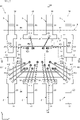
- FIG. 1 is a plan view showing a semiconductor device according to a first embodiment of the present disclosure
- FIG. FIG. 2 is a fragmentary plan view showing the semiconductor device according to the first embodiment of the present disclosure
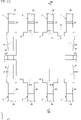
- FIG. FIG. 3 is a bottom view of essential parts showing the semiconductor device according to the first embodiment of the present disclosure.
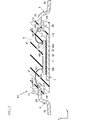
- FIG. 4 is a front view showing the semiconductor device according to the first embodiment of the present disclosure
- FIG. 5 is a side view showing the semiconductor device according to the first embodiment of the present disclosure
- FIG. FIG. 6 is a cross-sectional view taken along line VI-VI of FIG.
- FIG. 7 is a cross-sectional view along line VII-VII of FIG.
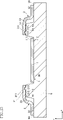
- FIG. 8 is an enlarged cross-sectional view of the main part showing the semiconductor device according to the first embodiment of the present disclosure.
- FIG. 9 is an enlarged bottom view of main parts showing the semiconductor device according to the first embodiment of the present disclosure.
- FIG. 10 is an enlarged cross-sectional view of the main part showing the semiconductor device according to the first embodiment of the present disclosure.
- FIG. 11 is an enlarged bottom view of main parts showing the semiconductor device according to the first embodiment of the present disclosure.
- FIG. 14 is an enlarged cross-sectional view of a main part showing the method of manufacturing the semiconductor device according to the first embodiment of the present disclosure.
- FIG. 15 is an enlarged cross-sectional view of a main part showing the method of manufacturing the semiconductor device according to the first embodiment of the present disclosure.
- FIG. 16 is a main part plan view showing the method of manufacturing the semiconductor device according to the first embodiment of the present disclosure; 17 is a cross-sectional view along line XVII-XVII of FIG. 16.
- FIG. 18A and 18B are cross-sectional views showing the method for manufacturing the semiconductor device according to the first embodiment of the present disclosure.
- 19A and 19B are cross-sectional views showing the method for manufacturing the semiconductor device according to the first embodiment of the present disclosure.
- FIG. 20 is an enlarged cross-sectional view of the main part showing the method of manufacturing the semiconductor device according to the first embodiment of the present disclosure.
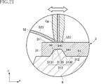
- FIG. 21 is an enlarged cross-sectional view of the main part showing the method of manufacturing the semiconductor device according to the first embodiment of the present disclosure.
- FIG. 22 is a main part plan view showing the method of manufacturing the semiconductor device according to the first embodiment of the present disclosure; 23 is a cross-sectional view taken along line XXIII-XXIII of FIG. 22.
- FIG. FIG. 24 is an enlarged cross-sectional view of main parts showing a modification of the method for manufacturing the semiconductor device according to the first embodiment of the present disclosure.
- FIG. 25 is an enlarged bottom view of main parts showing a modification of the semiconductor device according to the first embodiment of the present disclosure.
- FIG. 26 is an enlarged bottom view of a main part showing a modification of the semiconductor device according to the first embodiment of the present disclosure
- FIG. 27 is an enlarged bottom view of a main part showing a modification of the semiconductor device according to the first embodiment of the present disclosure
- FIG. 28 is an enlarged cross-sectional view of a main part showing the manufacturing method of the modification of the semiconductor device according to the first embodiment of the present disclosure
- FIG. 29 is an enlarged bottom view of a main part showing a modification of the semiconductor device according to the first embodiment of the present disclosure
- FIG. 30 is an enlarged cross-sectional view of main parts of a modification of the semiconductor device according to the first embodiment of the present disclosure.
- FIG. 31 is an enlarged cross-sectional view of main parts showing a modification of the semiconductor device according to the first embodiment of the present disclosure.
- FIG. 32 is a cross-sectional view showing a semiconductor device according to a second embodiment of the present disclosure; 33A and 33B are cross-sectional views showing a method for manufacturing a semiconductor device according to the second embodiment of the present disclosure.
- a semiconductor device A1 of this embodiment includes a first lead 1, a plurality of second leads 2, a plurality of third leads 3, a semiconductor element 4, a plurality of first wires 51, a plurality of second wires 52, and a sealing resin 8. It has The shape and size of the semiconductor device A1 are not particularly limited. An example of the size of the semiconductor device A1 is about 4 mm to 7 mm in the x direction, about 4 mm to 8 mm in the y direction, and about 0.7 mm to 2.0 mm in the z direction. be.
- FIG. 1 is a plan view showing the semiconductor device A1.
- FIG. 2 is a fragmentary plan view showing the semiconductor device A1.
- FIG. 3 is a bottom view of essential parts showing the semiconductor device A1.
- FIG. 4 is a front view showing the semiconductor device A1.
- FIG. 5 is a side view showing the semiconductor device A1.
- 6 is a cross-sectional view taken along line VI-VI of FIG. 3.
- FIG. 7 is a cross-sectional view along line VII-VII of FIG.
- FIG. 8 is an enlarged cross-sectional view of a main part showing the semiconductor device A1.
- FIG. 9 is an enlarged bottom view of essential parts showing the semiconductor device A1.
- FIG. 10 is an enlarged cross-sectional view of a main part showing the semiconductor device A1.
- FIG. 10 is an enlarged cross-sectional view of a main part showing the semiconductor device A1.
- FIG. 11 is an enlarged bottom view of essential parts showing the semiconductor device A1. 2 and 3, the sealing resin 8 is indicated by imaginary lines for convenience of understanding, and the covering portion 7 is omitted in FIG. 3 for convenience of understanding. 9 shows only part of the second lead 2, and FIG. 11 shows only part of the third lead 3. As shown in FIG.
- the first lead 1 is a member that supports the semiconductor element 4 and constitutes a conduction path to the semiconductor element 4 .
- the material of first lead 1 is not particularly limited, and is made of, for example, metals represented by Cu, Ni, Fe, etc., and alloys thereof.
- the first lead 1 may be formed with a plated layer made of a metal represented by Ag, Ni, Pd, Au, etc., at an appropriate position.
- the thickness of first lead 1 is not particularly limited, and is, for example, about 0.12 mm to 0.2 mm.
- the first lead 1 of this embodiment has a die pad portion 11 and two extension portions 12 .
- the die pad portion 11 is a portion that supports the semiconductor element 4 .
- the shape of the die pad portion 11 is not particularly limited, and is rectangular when viewed in the z direction in this embodiment.
- the die pad portion 11 has a die pad main surface 111 and a die pad back surface 112 .
- the die pad main surface 111 is a surface facing the z direction.
- the die pad back surface 112 is a surface facing away from the die pad main surface 111 in the thickness direction. In the illustrated example, die pad main surface 111 and die pad back surface 112 are planar.
- the two extending portions 12 are portions extending from the die pad portion 11 to opposite sides in the x direction.
- the extending portion 12 includes a portion extending from the die pad portion 11 along the x direction, a portion extending obliquely in the z direction toward the die pad main surface 111 with respect to the portion, and a portion extending from the portion extending in the z direction. It has a portion extending along the x-direction, and has a bent shape as a whole.
- the plurality of second leads 2 are separated from the first leads 1 and constitute a conductive path to the semiconductor element 4 .
- the plurality of second leads 2 constitute conduction paths for currents switched by the semiconductor element 4 .
- a plurality of second leads 2 are arranged on one side of the first leads 1 in the y direction. Also, the plurality of second leads 2 are arranged apart from each other in the x direction.
- the material of the second lead 2 is not particularly limited, and is made of, for example, metals represented by Cu, Ni, Fe, etc., and alloys thereof. Moreover, the second lead 2 may be formed with a plated layer made of a metal represented by Ag, Ni, Pd, Au, etc., at an appropriate position. The thickness of second lead 2 is not particularly limited, and is, for example, about 0.12 mm to 0.2 mm.
- the second lead 2 of this embodiment has a bonding pad portion 21 , a terminal portion 22 and a connecting portion 23 .
- the bonding pad portion 21 is a portion to which the first wire 51 is connected.
- the bonding pad portion 21 is located on the side (upper side in the figure) on which the die pad main surface 111 faces the die pad portion 11 in the z direction.
- the bonding pad portion 21 has a bonding pad main surface 211 , a bonding pad back surface 212 and a first portion 213 .
- the bonding pad main surface 211 faces the same side as the die pad main surface 111 in the z direction. It is preferable that all or part of the bonding pad main surface 211 is provided with the plating layer described above.
- the bonding pad main surface 211 is located on the side (upper side in the figure) facing the die pad main surface 111 with respect to the die pad main surface 111 in the z direction.
- the bonding pad back surface 212 is a surface facing the opposite side of the bonding pad main surface 211 in the z direction.
- the bonding pad back surface 212 is located on the side (upper side in the figure) on which the die pad main surface 111 faces the die pad back surface 112 in the z direction.
- the first portion 213 is connected to the bonding pad rear surface 212 and is surrounded by the bonding pad rear surface 212 when viewed in the z direction.
- the first portion 213 includes a portion located at a different position from the bonding pad back surface 212 in the z-direction.
- a specific configuration of the first part 213 is not particularly limited.
- the first portion 213 of this embodiment is a concave portion having an opening edge 2130 on the bonding pad rear surface 212 and recessed toward the bonding pad main surface 211 side in the z direction.
- a specific configuration of the first portion 213 configured by the concave portion is not particularly limited.
- the first portion 213 has an open edge 2130 , a first surface 2131 and a bottom surface 2135 .
- the opening edge 2130 is the edge that contacts the bonding pad back surface 212 .
- the shape of the opening edge 2130 is not particularly limited, and various shapes such as circular, elliptical, and polygonal may be adopted as appropriate. In the illustrated example, the opening edge 2130 is circular.
- the first surface 2131 is a surface that is inclined away from the bonding pad rear surface 212 as viewed in the z direction as it separates from the bonding pad rear surface 212 toward the bonding pad main surface 211 in the z direction.
- the shape and size of the first surface 2131 are not particularly limited.
- the angle ⁇ 1 is the angle formed between the first surface 2131 and the xy plane, which is a plane perpendicular to the z direction.
- the angle ⁇ 1 is preferably 25° or more and 50° or less, for example.
- the first surface 2131 has an annular shape when viewed in the z direction, and more specifically has an annular shape. Since the first surface 2131 is such an inclined surface, the portion of the recessed first portion 213 other than the opening edge 2130 is located inside the opening edge 2130 when viewed in the z direction.
- the bottom surface 2135 is the surface of the first portion 213 that is closest to the bonding pad main surface 211 in the z direction.
- the specific shape and size of the bottom surface 2135 are not particularly limited, and various shapes such as circular, elliptical, and polygonal are appropriately employed. In the illustrated example, the bottom surface 2135 is circular.
- the depth in the z direction of the first portion 213 is 1/4 or more and 1/2 or less of the thickness of the bonding pad portion 21 (second lead 2).
- the diameter of the opening edge 2130 is 0.5 times or more the thickness of the bonding pad portion 21 (second lead 2). 5 times or less.
- the terminal portion 22 is a belt-like portion extending in the y direction outside the sealing resin 8 .
- the terminal portion 22 is arranged at a position overlapping the die pad portion 11 when viewed in the y direction.
- the connecting portion 23 is a portion that connects the bonding pad portion 21 and the terminal portion 22 .
- the connecting portion 23 has a bent shape when viewed in the x direction.
- the connecting portion 23 includes a portion covered with the sealing resin 8 and a portion exposed from the sealing resin 8 .
- the plurality of third leads 3 are separated from the first leads 1 and constitute a conductive path to the semiconductor element 4 .
- the plurality of third leads 3 constitute conduction paths for control signal currents for controlling the semiconductor element 4 .
- a plurality of third leads 3 are arranged on the other side in the y direction with respect to the first leads 1 . Also, the plurality of third leads 3 are arranged apart from each other in the x direction.
- the material of the third lead 3 is not particularly limited, and is made of, for example, metals represented by Cu, Ni, Fe, etc., and alloys thereof. Also, the third lead 3 may be formed with a plated layer made of a metal represented by Ag, Ni, Pd, Au, etc., at an appropriate position. The thickness of the third lead 3 is not particularly limited, and is, for example, approximately 0.12 mm to 0.2 mm.
- the third lead 3 of this embodiment has a bonding pad portion 31 , a terminal portion 32 and a connecting portion 33 .
- the bonding pad portion 31 is a portion to which the second wire 52 is connected.
- the bonding pad portion 31 is located on the side (upper side in the figure) on which the die pad main surface 111 faces the die pad portion 11 in the z direction.
- the bonding pad portion 31 has a bonding pad main surface 311 , a bonding pad back surface 312 and a third portion 313 .
- the bonding pad main surface 311 faces the same side as the die pad main surface 111 in the z direction. It is preferable that all or part of the bonding pad main surface 311 is provided with the plating layer described above.
- the bonding pad main surface 311 is located on the side (upper side in the figure) facing the die pad main surface 111 with respect to the die pad main surface 111 in the z direction.
- the bonding pad back surface 312 is a surface facing the opposite side of the bonding pad main surface 311 in the z direction.
- the bonding pad back surface 312 is located on the side (upper side in the figure) on which the die pad main surface 111 faces the die pad back surface 112 in the z direction.
- the third portion 313 is connected to the bonding pad rear surface 312 and is surrounded by the bonding pad rear surface 312 when viewed in the z direction.
- the third portion 313 includes a portion located at a different position from the bonding pad back surface 312 in the z-direction.
- a specific configuration of the third part 313 is not particularly limited.
- the third portion 313 of this embodiment is a concave portion having an opening edge 3130 on the bonding pad rear surface 312 and recessed toward the bonding pad main surface 311 side in the z direction.
- the specific configuration of the third portion 313 configured by recesses is not particularly limited.
- the third portion 313 has an open edge 3130 , a first surface 3131 and a bottom surface 3135 .
- the opening edge 3130 is the edge that contacts the bonding pad back surface 312 .
- the shape of the opening edge 3130 is not particularly limited, and various shapes such as circular, elliptical, and polygonal may be adopted as appropriate. In the illustrated example, the opening edge 3130 is circular.
- the first surface 3131 is a surface that is inclined away from the bonding pad rear surface 312 as viewed in the z direction as it separates from the bonding pad rear surface 312 toward the bonding pad main surface 311 in the z direction.
- the shape and size of the first surface 3131 are not particularly limited.
- the angle ⁇ 2 is the angle between the first surface 3131 and the xy plane, which is a plane perpendicular to the z direction.
- the angle ⁇ 2 is preferably, for example, 25° or more and 50° or less.
- the first surface 3131 has an annular shape when viewed in the z-direction, and more specifically has an annular shape. Since the first surface 3131 is such an inclined surface, the portion other than the opening edge 3130 of the recessed third portion 313 is located inside the opening edge 3130 when viewed in the z direction.
- the bottom surface 3135 is the surface of the third portion 313 that is closest to the bonding pad main surface 311 in the z direction.
- the specific shape and size of the bottom surface 3135 are not particularly limited, and various shapes such as circular, elliptical, and polygonal may be adopted as appropriate. In the illustrated example, the bottom surface 3135 is circular.
- the depth in the z direction of the third portion 313 is 1/4 or more and 1/2 or less of the thickness of the bonding pad portion 31 (third lead 3).
- the diameter of the opening edge 3130 is 0.5 times or more the thickness of the bonding pad portion 31 (third lead 3). 5 times or less.
- the terminal portion 32 is a belt-like portion extending in the y direction outside the sealing resin 8 .
- the terminal portion 32 is arranged at a position overlapping the die pad portion 11 when viewed in the y direction.
- the connecting portion 33 is a portion that connects the bonding pad portion 31 and the terminal portion 32 .
- the connecting portion 33 has a bent shape when viewed in the x direction.
- the connecting portion 33 includes a portion covered with the sealing resin 8 and a portion exposed from the sealing resin 8 .
- the semiconductor element 4 is an element that exhibits the electrical functions of the semiconductor device A1.
- the specific configuration of the semiconductor element 4 is not particularly limited, and various types of semiconductor elements can be selected as appropriate.
- the semiconductor element 4 performs a switching function.
- the semiconductor element 4 has an element body 40 , first electrodes 401 , second electrodes 402 and a plurality of third electrodes 403 .
- the semiconductor device 4 also has a control section 48 .
- the semiconductor element 4 has a portion that constitutes a transistor that performs a switching function, and a portion that controls, monitors, protects, etc. the transistor.
- the specific configuration of the semiconductor element 4 is not particularly limited.
- the semiconductor element 4 may have a functional layer 408 or the like as a portion that constitutes a transistor, and may have a configuration without the control section 48 .
- the number and presence/absence of the second electrodes 402 and the third electrodes 403 are appropriately selected.
- other semiconductor elements may be mounted on the die pad portion 11 in addition to the semiconductor element 4 .
- the functions of the semiconductor elements other than the semiconductor element 4 are not particularly limited.
- the element main body 40 has an element main surface 40a and an element back surface 40b.
- the element main surface 40a faces the same side as the die pad main surface 111 in the z direction.
- the element back surface 40b is a surface that faces the side opposite to the element main surface 40a in the z direction.
- the material of the element main body 40 is not particularly limited. Examples of materials for the element body 40 include semiconductor materials such as Si, SiC, and GaN.
- the element body 40 has a functional layer 408, for example, as shown in FIG.
- the functional layer 408 has a transistor structure typified by, for example, a MOSFET (Metal Oxide Semiconductor Field Effect Transistor), a MISFET (Metal Insulator Semiconductor Field Effect Transistor), and the like.
- the functional layer 408 is arranged side by side with the control unit 48 in the y direction when viewed in the z direction.
- the specific arrangement of the functional layer 408 and the controller 48 is not particularly limited.
- the first electrode 401 is arranged on the element main surface 40 a of the element body 40 .
- the shape, size and position of the first electrode 401 are not particularly limited.
- the first electrode 401 is arranged on a portion of the element main surface 40a on the side of the plurality of second leads 2 in the y direction.
- the first electrode 401 overlaps the functional layer 408 when viewed in the z direction.
- the first electrode 401 is separated from the control section 48 when viewed in the z direction.
- the first electrode 401 is the source electrode.
- the material of the first electrode 401 is not particularly limited, and examples thereof include metals represented by Al (aluminum), Al—Si, Cu (copper), and alloys containing these.
- the first electrode 401 may have a structure in which layers made of a plurality of materials selected from these metals are laminated.
- the second electrode 402 is arranged on the element back surface 40 b of the element body 40 .
- the second electrode 402 overlaps the functional layer 408 and the control section 48 when viewed in the z-direction, and covers the entire back surface 40b of the element in this embodiment.
- the second electrode 402 is the drain electrode.
- the material of the second electrode 402 is not particularly limited, and examples thereof include metals represented by Al, Al--Si, Cu, etc., and alloys containing these.
- the second electrode 402 may have a structure in which layers made of a plurality of materials selected from these metals are laminated.
- Control unit 48 includes, for example, a current sensor circuit, a temperature sensor circuit, an overcurrent protection circuit, an overheating protection circuit, a low voltage malfunction prevention circuit, and the like.
- the plurality of third electrodes 403 are arranged on the element main surface 40a.
- the plurality of third electrodes 403 are arranged on the portion of the element main surface 40a on the side of the plurality of third leads 3 in the y direction.
- the plurality of third electrodes 403 overlap the control section 48 when viewed in the z direction.
- the plurality of third electrodes 403 are mainly electrically connected to the controller 48 .
- the number of the multiple third electrodes 403 is not particularly limited. Also, the number of third electrodes 403 may be one.
- the semiconductor element 4 has four third electrodes 403 .
- the plurality of first wires 51 electrically connect the first electrodes 401 of the semiconductor element 4 and the plurality of second leads 2 .
- the material of first wire 51 is not particularly limited, and is made of metal represented by Au, Cu, Al, or the like, for example.
- the first wire 51 of this embodiment has a bonding portion 511 , a bonding portion 512 and a loop portion 513 .
- a specific configuration of the first wire 51 is not particularly limited.
- first wire 51 is made of a material containing Cu, and is formed by a capillary, for example. In this embodiment, a current switched by the semiconductor element 4 flows through the plurality of first wires 51 .
- the bonding portion 511 is bonded to the first electrode 401 of the semiconductor element 4 and arranged at a position overlapping the first electrode 401 when viewed in the z direction.
- the bonding portion 511 is a so-called first bonding portion.
- the arrangement of the bonding portion 511 is not particularly limited.
- the bonding portions 511 of the plurality of first wires 51 are distributed over substantially the entire area of the first electrode 401 .
- the bonding portions 511 of the plurality of first wires 51 may be arranged in one or more rows along the outer peripheral edge of the first electrode 401, for example.
- the bonding portion 512 is a portion that is bonded to the bonding pad main surface 211 of the bonding pad portion 21 of the second lead 2 .
- the bonding portion 512 is a so-called second bonding portion.
- a plurality of bonding portions 512 are arranged on one bonding pad portion 21 . Any one of the plurality of bonding portions 512 bonded to one bonding pad portion 21 and the first portion 213 preferably partially overlap each other when viewed in the z direction. However, the plurality of bonding portions 512 bonded to one bonding pad portion 21 and the first portion 213 may be configured so as not to overlap when viewed in the z direction.
- the loop portion 513 is connected to the bonding portion 511 and the bonding portion 512 and has a curved shape.
- the plurality of second wires 52 electrically connect the third electrodes 403 of the semiconductor element 4 and the plurality of third leads 3 .
- the material of the second wire 52 is not particularly limited, and is made of metal represented by Au, Cu, Al, or the like, for example.
- the second wire 52 has a bonding portion 521 , a bonding portion 522 and a loop portion 523 .
- a specific configuration of the second wire 52 is not particularly limited.
- the second wire 52 is formed by a capillary, for example.
- a control signal current for controlling the semiconductor element 4 flows through the plurality of second wires 52 .
- the bonding portion 521 is joined to the second electrode 402 of the semiconductor element 4 .
- the bonding portion 521 is a so-called first bonding portion.
- the bonding portion 522 is a portion that is bonded to the bonding pad main surface 311 of the bonding pad portion 31 of the third lead 3 .
- the bonding portion 522 is a so-called second bonding portion.
- one bonding portion 522 is arranged on one bonding pad portion 31 . It is preferable that the bonding portion 522 and the third portion 313 overlap each other at least partially when viewed in the z direction. Alternatively, the bonding portion 522 and the third portion 313 may be configured so that they do not overlap when viewed in the z direction.
- the loop portion 523 is connected to the bonding portion 521 and the bonding portion 522 and has a curved shape.
- the sealing resin 8 covers the first lead 1 , the plurality of second leads 2 , the plurality of third leads 3 , the semiconductor element 4 , the plurality of first wires 51 , the plurality of second wires 52 and the covering portion 7 . .
- a portion of the first lead 1, a portion of each second lead 2, and a portion of each third lead are exposed from the sealing resin 8.
- the encapsulating resin 8 is made of an insulating resin, and includes, for example, an epoxy resin mixed with a filler. Further, in this embodiment, part of the sealing resin 8 fills the first portion 213 of the second lead 2 and the third portion 313 of the third lead 3 .
- the shape of the sealing resin 8 is not particularly limited.
- the sealing resin 8 has a resin main surface 81 , a resin back surface 82 , two first resin side surfaces 83 and two second resin side surfaces 84 .
- the resin main surface 81 faces the same side as the die pad main surface 111 in the z direction, and is flat, for example.
- the resin back surface 82 is a surface facing the opposite side of the resin main surface 81 in the z-direction, and is, for example, a flat surface.
- the two first resin side surfaces 83 are located between the resin main surface 81 and the resin back surface 82 in the z direction, and face opposite sides in the x direction.
- the two second resin side surfaces 84 are positioned between the resin main surface 81 and the resin back surface 82 in the z direction, and face opposite sides in the y direction.
- FIG. 12 An example of a method for manufacturing the semiconductor device A1 will be described below with reference to FIGS. 12 to 22.
- FIG. 12 An example of a method for manufacturing the semiconductor device A1 will be described below with reference to FIGS. 12 to 22.
- a first lead 1, a plurality of second leads 2 and a plurality of third leads 3 are prepared.
- the first lead 1, the plurality of second leads 2, and the plurality of third leads 3 may be individually separated, or a lead frame having a frame (not shown) connecting them may be used. may be used.
- a lead frame is used, after the steps described below are completed, the lead frame is cut at appropriate locations to obtain the first lead 1, the plurality of second leads 2 and the plurality of third leads 3 which are separated into pieces. can get.
- a first lead 1 , a plurality of second leads 2 and a third lead 3 are supported by a support 9 .
- the support 9 is a member made of metal or the like, for example.
- the specific configuration of the support 9 is not particularly limited, and has a base surface 90 , a support surface 91 , a second portion 92 , a support surface 93 and a fourth portion 94 in this embodiment.
- the base surface 90 is a surface that occupies most of the area of the support 9, and faces the upper side in the figure (the side to which the die pad main surface 111 faces) in the z direction.
- the base surface 90 supports the die pad portion 11, the terminal portion 22, the terminal portion 32, and the like.
- the support surface 91 faces the upper side in the figure (the side to which the die pad main surface 111 faces) in the z direction, and is located above the base surface 90 in the figure (the side to which the die pad main surface 111 faces).
- the support surface 91 supports the bonding pad portion 21 and is in contact with the bonding pad rear surface 212 .
- the second part 92 is a part that engages with the first part 213 of the bonding pad part 21 of the second lead 2 .
- the specific configuration of the second portion 92 is not particularly limited, and in the illustrated example, it is a truncated conical projection corresponding to the configuration of the first portion 213 described above.
- This second part 92 has a first surface 921 and a top surface 925 .
- the first surface 921 is a surface that faces the first surface 2131 and can come into contact therewith. Like the first surface 2131, the first surface 921 is inclined by an angle ⁇ 1 (or 180° ⁇ angle ⁇ 1) with respect to the xy plane. Also, the first surface 921 has an annular shape when viewed in the z-direction, like the first surface 2131 .
- the top surface 925 is a tip surface of the second portion 92 that is a convex portion, and is a surface that faces the bottom surface 2135 and can come into contact therewith.
- the top surface 925 is circular, corresponding to the bottom surface 2135 .
- the support surface 93 faces the upper side in the drawing (the side to which the die pad main surface 111 faces) in the z direction, and is located above the base surface 90 in the drawing (the side to which the die pad main surface 111 faces).
- the support surface 93 supports the bonding pad portion 31 and is in contact with the bonding pad rear surface 312 .
- the fourth portion 94 is a portion that engages with the third portion 313 of the bonding pad portion 31 of the third lead 3 .
- the specific configuration of the fourth portion 94 is not particularly limited, and in the illustrated example, it is a truncated conical projection corresponding to the configuration of the third portion 313 described above.
- This fourth portion 94 has a first surface 941 and a top surface 945 .
- the first surface 941 is a surface that faces the first surface 3131 and can come into contact therewith. Like the first surface 3131, the first surface 941 is inclined by an angle ⁇ 2 (or 180° ⁇ angle ⁇ 2) with respect to the xy plane. Also, the first surface 941 has an annular shape when viewed in the z-direction, like the first surface 3131 .
- the top surface 945 is the tip surface of the fourth portion 94 that is a convex portion, and is a surface that faces the bottom surface 3135 and can come into contact therewith.
- the top surface 945 is circular, corresponding to the bottom surface 3135 .
- the semiconductor element 4 is mounted on the first lead 1. Then, as shown in FIGS. Specifically, the second electrode 402 of the semiconductor element 4 and the die pad main surface 111 of the die pad portion 11 of the first lead 1 are bonded using a bonding paste as a material of the bonding material 49 .
- the plurality of first wires 51 and the plurality of second wires 52 are bonded.
- the order of bonding the plurality of first wires 51 and the plurality of second wires 52 is not particularly limited.
- the plurality of second wires 52 may be bonded after all the first wires 51 are bonded, or the plurality of first wires 51 may be bonded after all the second wires 52 are bonded.
- the first wires 51 and the second wires 52 may be alternately bonded.
- first, bonding of the first wire 51 will be described.
- the bonding of the second wire 52 is performed in a manner similar to the bonding of the first wire 51 .
- first bonding is performed on the first electrode 401 using a capillary Cp.
- the capillary Cp holds the wire material 510 so that it can move back and forth.
- a predetermined amount of wire material 510 is protruded from the capillary Cp and melted.
- the molten wire material 510 is attached to the first electrode 401 .
- a bonding portion 511 is formed.
- the capillary Cp is brought closer to the bonding pad portion 21 of the second lead 2 along a predetermined path. Thereby, the loop portion 513 shown in FIG. 19 is formed. Then, the wire material 510 is pressed against the bonding pad main surface 211 of the bonding pad portion 21 by the capillary Cp. At this time, it is preferable to press the wire material 510 to a position overlapping the first portion 213 when viewed in the z direction. However, the wire material 510 may be pressed to a position that does not overlap the first portion 213 . Then, as shown in FIG. 20, force and vibration are applied to the wire material 510 from the capillary Cp.
- This vibration is, for example, ultrasonic vibration.
- wire material 510 is bonded to bonding pad main surface 211 .
- the capillary Cp is separated upward in the z-direction from the bonding pad portion 21 in a state in which the wire material 510 is not extended.
- the first wire 51 having the bonding portion 511, the bonding portion 512 and the loop portion 513 is formed.
- the formation of the second wire 52 is performed using a capillary Cp in the same manner as the first wire 51 .
- bonding portion 522 is formed on bonding pad main surface 311 of bonding pad portion 31 of third lead 3, as shown in FIG.
- the bonding portion 522 is formed by pressing the wire material 510 against the bonding pad main surface 311 of the bonding pad portion 31 by the capillary Cp, similarly to the formation of the bonding portion 512 .
- the wire material 510 may be pressed to a position overlapping the third portion 313 .
- a plurality of first wires 51 and a plurality of second wires 52 are formed as shown in FIGS.
- the first lead 1 , the plurality of second leads 2 , the plurality of third leads 3 , the semiconductor element 4 , the plurality of first wires 51 and the plurality of second wires 52 are separated from the support 9 .
- the sealing resin 8 is formed by, for example, mold molding. Thereby, the semiconductor device A1 described above is obtained.
- the bonding pad section 21 has the first section 213 .
- the first portion 213 engages the second portion 92 of the support 9, as shown in FIGS.
- the bonding pad portion 21 is unintentionally moved along the xy plane. It is possible to suppress misalignment. Therefore, according to this embodiment, the first wire 51 can be bonded more reliably.
- the first portion 213 overlaps the bonding portion 512 when viewed in the z direction. As a result, the force and vibration when forming the bonding portion 512 can be more reliably received by the engaging structure between the bonding portion 512 and the second portion 92 .
- the bonding portion 512 is the second bonding portion, a larger force and vibration are likely to be applied to the bonding pad portion 21 when the bonding portion 512 is formed.
- the bonding portion 512 which is the second bonding portion, can be formed more appropriately.
- the first part 213 is configured by a recess. This makes it possible to prevent the first part 213 from unintentionally interfering with other members or the like in the method of manufacturing the semiconductor device A1.
- the first surface 2131 of the first portion 213 is an inclined surface that is inclined away from the bonding pad rear surface 212 when viewed in the z direction as the distance from the bonding pad rear surface 212 increases in the z direction.
- the bonding pad portion 21 can be smoothly detached from the support 9 after the bonding of the first wire 51 is completed. can be done. Further, when the second lead 2 is supported by the support 9, even if the first portion 213 is arranged at a position slightly deviated from the second portion 92, the bonding pad portion 21 is positioned downward in the z direction.
- the angle ⁇ 1 is preferably 25° or more and 50° or less in order to more appropriately obtain the effect of the first surface 2131 being an inclined surface.
- the depth of the first portion 213 in the z-direction is 1/4 or more and 1/2 or less of the thickness of the second lead 2 (bonding pad portion 21) separates the first portion 213 and the second portion 92 from each other. This is preferable for avoiding an unreasonable decrease in rigidity of the bonding pad portion 21 while ensuring proper engagement.
- FIG. 24 shows a first modification of the method for manufacturing the semiconductor device A1.
- the first surface 2131 of the first portion 213 of the bonding pad portion 21 and the first surface 921 of the second portion 92 are in contact with each other, and the bottom surface 2135 of the first portion 213 and the second portion 92 are separated from each other by a gap. That is, in this modification, the height of the second portion 92 in the z direction is smaller than the depth of the first portion 213 in the z direction.
- the first wire 51 can be bonded more reliably.
- the specific configuration of the first portion 213 and the second portion 92 and the state of contact between the first portion 213 and the second portion 92 are not particularly limited. Also, the configurations of the first portion 213 and the second portion 92 to be described after the modification can be similarly applied to the third portion 313 and the fourth portion 94 .
- the height of the second portion 92 is smaller than the depth of the first portion 213, the back surface 212 of the bonding pad and the support surface 91 can be brought into contact with each other more reliably. Further, by making the size of the opening edge 2130 smaller than the size of the boundary between the second portion 92 and the support surface 91, the first surface 2131 and the first surface 921 can be brought into contact with each other more reliably. can be done. Thereby, in bonding the first wire 51 using the capillary Cp, it is possible to further suppress the bonding pad portion 21 from being shifted in the xy plane.
- FIG. 25 shows the first part 213 according to the second modified example of the semiconductor device A1.
- the first portion 213 of this modification has an opening edge 2130 , a first surface 2131 , a second surface 2132 , a third surface 2133 , a fourth surface 2134 and a bottom surface 2135 .
- the opening edge 2130 has a rectangular shape when viewed in the z direction.
- the first surface 2131, the second surface 2132, the third surface 2133, and the fourth surface 2134 are all inclined at an angle ⁇ 1, for example, with respect to the xy plane, like the first surface 2131 described above.
- the first surface 2131, the second surface 2132, the third surface 2133, and the fourth surface 2134 are arranged at different positions when viewed in the z direction.
- the first surface 2131, the second surface 2132, the third surface 2133, and the fourth surface 2134 are arranged to form a rectangular ring surrounding the bottom surface 2135 when viewed in the z direction.
- the first wire 51 can be bonded more reliably.
- the specific configuration of the first part 213 is not particularly limited.
- the shape and size of the second portion 92 that can be engaged may be appropriately adopted according to the shape and size of the first portion 213 .
- FIG. 26 shows the first part 213 according to the third modified example of the semiconductor device A1.
- the first part 213 of this modification has an open edge 2130 , a first surface 2131 , a second surface 2132 , a third surface 2133 and a bottom surface 2135 .
- the opening edge 2130 has a triangular shape when viewed in the z direction.
- the first surface 2131, the second surface 2132, and the third surface 2133 are all inclined at an angle ⁇ 1, for example, with respect to the xy plane, similarly to the first surface 2131 described above.
- the first surface 2131, the second surface 2132 and the third surface 2133 are arranged at different positions when viewed in the z direction.
- the first surface 2131, the second surface 2132 and the third surface 2133 are arranged to form a triangular ring surrounding the bottom surface 2135 when viewed in the z direction.
- the first wire 51 can be bonded more reliably.
- the specific configuration of the first part 213 is not particularly limited.
- the opening edge 2130 of the first portion 213 may be polygonal, for example.
- the first portion 213 of this variation has an open edge 2130 and a first surface 2131 and does not have the bottom surface 2135 described above.
- the first surface 2131 of this modified example has a conical shape.
- a truncated cone-shaped second portion 92 may be adopted.
- the first wire 51 can be bonded more reliably.
- the first portion 213 may have a shape that does not have the bottom surface 2135 .
- FIG. 29 shows the first part 213 according to the fifth modified example of the semiconductor device A1.
- the first portion 213 of this modified example has a first surface 2131, a second surface 2132, a third surface 2133 and a fourth surface 2134, and does not have a bottom surface 2135 as in the fourth modified example.
- the first part 213 has a pyramidal shape. Also according to this modification, the first wire 51 can be bonded more reliably.
- the first portion 213 of this modification has an open edge 2130 and a first surface 2131 .
- the first surface 2131 is entirely concave.
- the first portion 213 has a hemispherical shape (or a substantially hemispherical shape) as a whole.
- the angle ⁇ 1 of the portion of the first surface 2131 that is connected to the opening edge 2130 is preferably sufficiently smaller than 90°.
- the second part 92 may have a hemispherical shape (or a substantially hemispherical shape).
- the second portion 92 may have a hemispherical shape with a flat top surface 925 (see FIG. 14).
- the first wire 51 can be bonded more reliably.
- the first surface 2131 may be a concave curved surface or a convex curved surface.
- the semiconductor device A2 of this embodiment differs from the semiconductor device A1 described above in the configuration of the first portion 213 and the third portion 313 .
- the first portion 213 is configured by a convex portion projecting from the bonding pad back surface 212 toward the bonding pad back surface 212 in the z direction. Also in this embodiment, only one first portion 213 is provided in one bonding pad portion 21 . The first portion 213 is connected to the bonding pad rear surface 212 and is surrounded by the bonding pad rear surface 212 when viewed in the z direction. The first portion 213 of the present embodiment also has a configuration including a portion located at a different position from the bonding pad back surface 212 in the z direction.
- the third portion 313 is configured by a convex portion protruding from the bonding pad back surface 312 toward the bonding pad back surface 312 in the z direction. Also in this embodiment, only one third portion 313 is provided in one bonding pad portion 31 . Also, the third portion 313 is connected to the bonding pad rear surface 312 and is surrounded by the bonding pad rear surface 312 when viewed in the z direction. The third portion 313 of the present embodiment also has a configuration including a portion located at a different position from the bonding pad back surface 312 in the z direction.
- the second part 92 and the fourth part 94 are configured by concave portions that can be engaged with the first part 213 and the third part 313 are used.
- the engagement of the first part 213 and the second part 92 and the engagement of the third part 313 and the fourth part 94 are realized, and the first wire 51 and the second wire 51 are connected to each other. Bonding of wires 52 may be performed.
- the first wire 51 can be bonded more reliably.
- the first portion 213 and the third portion 313 may be configured by concave portions or may be configured by convex portions.
- the semiconductor device and the method of manufacturing the semiconductor device according to the present disclosure are not limited to the above-described embodiments.
- the specific configuration of the semiconductor device and the method of manufacturing the semiconductor device according to the present disclosure can be modified in various ways.
- the present disclosure includes embodiments described in the appendices below.
- Appendix 1 a semiconductor element having a device body containing a semiconductor and a first electrode disposed on the device body; a first lead on which the semiconductor element is mounted; a second lead; a first wire that electrically connects the semiconductor element and the second lead;
- the first lead includes a die pad portion having a die pad main surface and a die pad back surface facing opposite to each other in the thickness direction;
- the semiconductor element is mounted on the main surface of the die pad
- the second lead includes a bonding pad portion having a bonding pad main surface facing the same side as the die pad main surface in the thickness direction and a bonding pad back surface facing the side opposite to the bonding pad main surface;
- the back surface of the bonding pad is arranged on the side where the main surface of the die pad is located with respect to the back surface of the die pad in the thickness direction,
- the first wire is bonded to the first electrode and the main surface of the bonding pad,
- the bonding pad portion has only one first portion, and the first portion is connected to the bonding
- Appendix 2. the first wire has a bonding portion bonded to the main surface of the bonding pad, The semiconductor device according to appendix 1, wherein the bonding portion and the first portion at least partially overlap with each other when viewed in the thickness direction. Appendix 3.
- Appendix 4. The semiconductor device according to any one of appendices 1 to 3, wherein the first part is a recess having an opening edge on the back surface of the bonding pad.
- Appendix 5. The semiconductor device according to appendix 4, wherein a portion of the recess other than the opening edge is located inside the opening edge when viewed in the thickness direction. Appendix 6. 6.
- the semiconductor device according to appendix 5 wherein the recess includes a first surface that is inclined away from the back surface of the bonding pad when viewed in the thickness direction as it moves away from the back surface of the bonding pad in the thickness direction.
- Appendix 7. The semiconductor device according to appendix 6, wherein a first angle formed between the first surface and a plane orthogonal to the thickness direction is 25° or more and 50° or less.
- Appendix 8. 8.
- the recess is inclined away from the back surface of the bonding pad when viewed in the thickness direction as the recess is separated from the back surface of the bonding pad in the thickness direction, and is positioned at a different position from the first surface when viewed in the thickness direction.
- Appendix 6 or 7 comprising a second surface arranged on the .
- Appendix 10. 4 The semiconductor device according to any one of appendices 1 to 3, wherein the first part is a convex part protruding from the back surface of the bonding pad.
- Appendix 11. 11.
- the semiconductor device according to any one of appendices 1 to 10 further comprising a sealing resin that covers the semiconductor element and the first wire, and at least part of each of the first lead and the second lead.
- a first lead including a die pad portion having a die pad main surface and a die pad back surface facing opposite to each other in the thickness direction, and a bonding pad main surface and the bonding pad main surface facing the same side as the die pad main surface in the thickness direction.
- the back surface of the bonding pad is arranged on the side where the main surface of the die pad is located with respect to the back surface of the die pad in the thickness direction,
- the bonding pad portion has only one first portion, and the first portion is connected to the bonding pad back surface and surrounded by the bonding pad back surface when viewed in the thickness direction, and has the thickness including a portion arranged at a position different in direction from the back surface of
- Appendix 17. The method of manufacturing a semiconductor device according to appendix 16, wherein the first part is a recess having an opening edge on the back surface of the bonding pad. Appendix 18. 18. The method of manufacturing a semiconductor device according to appendix 17, wherein a portion of the recess other than the opening edge is located inside the opening edge when viewed in the thickness direction.
Landscapes
- Wire Bonding (AREA)
Priority Applications (4)
| Application Number | Priority Date | Filing Date | Title |
|---|---|---|---|
| DE112022000758.3T DE112022000758T5 (de) | 2021-04-01 | 2022-03-14 | Halbleiterbauteil und verfahren zum herstellen eines halbleiterbauteils |
| JP2023510872A JPWO2022209819A1 (https=) | 2021-04-01 | 2022-03-14 | |
| CN202280026359.9A CN117157755A (zh) | 2021-04-01 | 2022-03-14 | 半导体器件和半导体器件的制造方法 |
| US18/478,122 US20240030178A1 (en) | 2021-04-01 | 2023-09-29 | Semiconductor device and manufacturing method for semiconductor device |
Applications Claiming Priority (2)
| Application Number | Priority Date | Filing Date | Title |
|---|---|---|---|
| JP2021-062894 | 2021-04-01 | ||
| JP2021062894 | 2021-04-01 |
Related Child Applications (1)
| Application Number | Title | Priority Date | Filing Date |
|---|---|---|---|
| US18/478,122 Continuation US20240030178A1 (en) | 2021-04-01 | 2023-09-29 | Semiconductor device and manufacturing method for semiconductor device |
Publications (1)
| Publication Number | Publication Date |
|---|---|
| WO2022209819A1 true WO2022209819A1 (ja) | 2022-10-06 |
Family
ID=83458909
Family Applications (1)
| Application Number | Title | Priority Date | Filing Date |
|---|---|---|---|
| PCT/JP2022/011312 Ceased WO2022209819A1 (ja) | 2021-04-01 | 2022-03-14 | 半導体装置および半導体装置の製造方法 |
Country Status (5)
| Country | Link |
|---|---|
| US (1) | US20240030178A1 (https=) |
| JP (1) | JPWO2022209819A1 (https=) |
| CN (1) | CN117157755A (https=) |
| DE (1) | DE112022000758T5 (https=) |
| WO (1) | WO2022209819A1 (https=) |
Citations (8)
| Publication number | Priority date | Publication date | Assignee | Title |
|---|---|---|---|---|
| JPH05175266A (ja) * | 1991-12-20 | 1993-07-13 | Mitsubishi Electric Corp | 半導体装置 |
| JP2001168261A (ja) * | 1999-12-03 | 2001-06-22 | Mitsui High Tec Inc | 半導体装置 |
| JP2001185671A (ja) * | 1999-12-22 | 2001-07-06 | Mitsubishi Electric Corp | 半導体装置の製造方法及び該半導体装置の製造に用いられるリードフレームの製造方法 |
| JP2001339029A (ja) * | 2000-05-26 | 2001-12-07 | Shinko Electric Ind Co Ltd | 多層リードフレーム及びこれを用いた半導体装置 |
| JP2003017524A (ja) * | 2001-06-28 | 2003-01-17 | Matsushita Electric Ind Co Ltd | 樹脂封止型半導体装置の製造方法 |
| JP2005166943A (ja) * | 2003-12-02 | 2005-06-23 | Sony Corp | リードフレーム、それを用いた半導体装置の製造におけるワイヤーボンディング方法及び樹脂封止型半導体装置 |
| JP2005191240A (ja) * | 2003-12-25 | 2005-07-14 | Renesas Technology Corp | 半導体装置及びその製造方法 |
| JP2008130660A (ja) * | 2006-11-17 | 2008-06-05 | Matsushita Electric Ind Co Ltd | 半導体装置の製造方法 |
Family Cites Families (2)
| Publication number | Priority date | Publication date | Assignee | Title |
|---|---|---|---|---|
| US7838339B2 (en) * | 2008-04-04 | 2010-11-23 | Gem Services, Inc. | Semiconductor device package having features formed by stamping |
| JP6857035B2 (ja) | 2017-01-12 | 2021-04-14 | ローム株式会社 | 半導体装置 |
-
2022
- 2022-03-14 WO PCT/JP2022/011312 patent/WO2022209819A1/ja not_active Ceased
- 2022-03-14 DE DE112022000758.3T patent/DE112022000758T5/de not_active Ceased
- 2022-03-14 JP JP2023510872A patent/JPWO2022209819A1/ja active Pending
- 2022-03-14 CN CN202280026359.9A patent/CN117157755A/zh active Pending
-
2023
- 2023-09-29 US US18/478,122 patent/US20240030178A1/en active Pending
Patent Citations (8)
| Publication number | Priority date | Publication date | Assignee | Title |
|---|---|---|---|---|
| JPH05175266A (ja) * | 1991-12-20 | 1993-07-13 | Mitsubishi Electric Corp | 半導体装置 |
| JP2001168261A (ja) * | 1999-12-03 | 2001-06-22 | Mitsui High Tec Inc | 半導体装置 |
| JP2001185671A (ja) * | 1999-12-22 | 2001-07-06 | Mitsubishi Electric Corp | 半導体装置の製造方法及び該半導体装置の製造に用いられるリードフレームの製造方法 |
| JP2001339029A (ja) * | 2000-05-26 | 2001-12-07 | Shinko Electric Ind Co Ltd | 多層リードフレーム及びこれを用いた半導体装置 |
| JP2003017524A (ja) * | 2001-06-28 | 2003-01-17 | Matsushita Electric Ind Co Ltd | 樹脂封止型半導体装置の製造方法 |
| JP2005166943A (ja) * | 2003-12-02 | 2005-06-23 | Sony Corp | リードフレーム、それを用いた半導体装置の製造におけるワイヤーボンディング方法及び樹脂封止型半導体装置 |
| JP2005191240A (ja) * | 2003-12-25 | 2005-07-14 | Renesas Technology Corp | 半導体装置及びその製造方法 |
| JP2008130660A (ja) * | 2006-11-17 | 2008-06-05 | Matsushita Electric Ind Co Ltd | 半導体装置の製造方法 |
Also Published As
| Publication number | Publication date |
|---|---|
| US20240030178A1 (en) | 2024-01-25 |
| DE112022000758T5 (de) | 2023-11-16 |
| JPWO2022209819A1 (https=) | 2022-10-06 |
| CN117157755A (zh) | 2023-12-01 |
Similar Documents
| Publication | Publication Date | Title |
|---|---|---|
| US10312171B2 (en) | Semiconductor device | |
| EP3544053B1 (en) | Discrete power transistor package having solderless dbc to leadframe attach | |
| CN104641459B (zh) | 半导体装置 | |
| JP4614586B2 (ja) | 混成集積回路装置の製造方法 | |
| JP2012015202A (ja) | 半導体装置およびその製造方法 | |
| JP2026048943A (ja) | 半導体装置 | |
| CN108022900A (zh) | 半导体装置 | |
| JP7137955B2 (ja) | 半導体装置 | |
| JP2019121698A (ja) | 半導体装置および半導体装置の製造方法 | |
| JP7594950B2 (ja) | 半導体装置 | |
| WO2023282013A1 (ja) | 半導体装置 | |
| JP2021158180A (ja) | 半導体装置 | |
| JP6923614B2 (ja) | 半導体装置 | |
| JP2011204863A (ja) | 半導体装置およびその製造方法 | |
| WO2022209819A1 (ja) | 半導体装置および半導体装置の製造方法 | |
| KR20160085672A (ko) | 초음파 용접을 이용한 반도체 패키지 및 제조 방법 | |
| JP2022074290A (ja) | 半導体装置 | |
| JP7842740B2 (ja) | 半導体装置 | |
| JP2003209132A (ja) | リードフレーム組立体及びそれを使用した半導体装置 | |
| JP7594952B2 (ja) | 半導体装置 | |
| JP2019145625A (ja) | 半導体装置 | |
| JP2023127285A (ja) | 半導体装置 | |
| WO2021215472A1 (ja) | 半導体装置 | |
| JP7630321B2 (ja) | 半導体装置 | |
| JP7630322B2 (ja) | 半導体装置 |
Legal Events
| Date | Code | Title | Description |
|---|---|---|---|
| 121 | Ep: the epo has been informed by wipo that ep was designated in this application |
Ref document number: 22780040 Country of ref document: EP Kind code of ref document: A1 |
|
| WWE | Wipo information: entry into national phase |
Ref document number: 2023510872 Country of ref document: JP |
|
| WWE | Wipo information: entry into national phase |
Ref document number: 112022000758 Country of ref document: DE |
|
| 122 | Ep: pct application non-entry in european phase |
Ref document number: 22780040 Country of ref document: EP Kind code of ref document: A1 |