WO2022196408A1 - 光硬化性組成物及びパターン形成方法 - Google Patents
光硬化性組成物及びパターン形成方法 Download PDFInfo
- Publication number
- WO2022196408A1 WO2022196408A1 PCT/JP2022/009681 JP2022009681W WO2022196408A1 WO 2022196408 A1 WO2022196408 A1 WO 2022196408A1 JP 2022009681 W JP2022009681 W JP 2022009681W WO 2022196408 A1 WO2022196408 A1 WO 2022196408A1
- Authority
- WO
- WIPO (PCT)
- Prior art keywords
- component
- group
- photocurable composition
- meth
- photocurable
- Prior art date
- Legal status (The legal status is an assumption and is not a legal conclusion. Google has not performed a legal analysis and makes no representation as to the accuracy of the status listed.)
- Ceased
Links
Images

Classifications
-
- C—CHEMISTRY; METALLURGY
- C08—ORGANIC MACROMOLECULAR COMPOUNDS; THEIR PREPARATION OR CHEMICAL WORKING-UP; COMPOSITIONS BASED THEREON
- C08F—MACROMOLECULAR COMPOUNDS OBTAINED BY REACTIONS ONLY INVOLVING CARBON-TO-CARBON UNSATURATED BONDS
- C08F2/00—Processes of polymerisation
- C08F2/46—Polymerisation initiated by wave energy or particle radiation
- C08F2/48—Polymerisation initiated by wave energy or particle radiation by ultraviolet or visible light
- C08F2/50—Polymerisation initiated by wave energy or particle radiation by ultraviolet or visible light with sensitising agents
-
- C—CHEMISTRY; METALLURGY
- C08—ORGANIC MACROMOLECULAR COMPOUNDS; THEIR PREPARATION OR CHEMICAL WORKING-UP; COMPOSITIONS BASED THEREON
- C08F—MACROMOLECULAR COMPOUNDS OBTAINED BY REACTIONS ONLY INVOLVING CARBON-TO-CARBON UNSATURATED BONDS
- C08F22/00—Homopolymers and copolymers of compounds having one or more unsaturated aliphatic radicals each having only one carbon-to-carbon double bond, and at least one being terminated by a carboxyl radical and containing at least one other carboxyl radical in the molecule; Salts, anhydrides, esters, amides, imides or nitriles thereof
- C08F22/10—Esters
- C08F22/12—Esters of phenols or saturated alcohols
- C08F22/24—Esters containing sulfur
-
- B—PERFORMING OPERATIONS; TRANSPORTING
- B29—WORKING OF PLASTICS; WORKING OF SUBSTANCES IN A PLASTIC STATE IN GENERAL
- B29C—SHAPING OR JOINING OF PLASTICS; SHAPING OF MATERIAL IN A PLASTIC STATE, NOT OTHERWISE PROVIDED FOR; AFTER-TREATMENT OF THE SHAPED PRODUCTS, e.g. REPAIRING
- B29C59/00—Surface shaping of articles, e.g. embossing; Apparatus therefor
- B29C59/005—Surface shaping of articles, e.g. embossing; Apparatus therefor characterised by the choice of material
-
- C—CHEMISTRY; METALLURGY
- C08—ORGANIC MACROMOLECULAR COMPOUNDS; THEIR PREPARATION OR CHEMICAL WORKING-UP; COMPOSITIONS BASED THEREON
- C08F—MACROMOLECULAR COMPOUNDS OBTAINED BY REACTIONS ONLY INVOLVING CARBON-TO-CARBON UNSATURATED BONDS
- C08F2/00—Processes of polymerisation
- C08F2/44—Polymerisation in the presence of compounding ingredients, e.g. plasticisers, dyestuffs, fillers
-
- C—CHEMISTRY; METALLURGY
- C08—ORGANIC MACROMOLECULAR COMPOUNDS; THEIR PREPARATION OR CHEMICAL WORKING-UP; COMPOSITIONS BASED THEREON
- C08F—MACROMOLECULAR COMPOUNDS OBTAINED BY REACTIONS ONLY INVOLVING CARBON-TO-CARBON UNSATURATED BONDS
- C08F2/00—Processes of polymerisation
- C08F2/46—Polymerisation initiated by wave energy or particle radiation
- C08F2/48—Polymerisation initiated by wave energy or particle radiation by ultraviolet or visible light
-
- C—CHEMISTRY; METALLURGY
- C08—ORGANIC MACROMOLECULAR COMPOUNDS; THEIR PREPARATION OR CHEMICAL WORKING-UP; COMPOSITIONS BASED THEREON
- C08K—Use of inorganic or non-macromolecular organic substances as compounding ingredients
- C08K3/00—Use of inorganic substances as compounding ingredients
- C08K3/18—Oxygen-containing compounds, e.g. metal carbonyls
- C08K3/20—Oxides; Hydroxides
- C08K3/22—Oxides; Hydroxides of metals
-
- G—PHYSICS
- G03—PHOTOGRAPHY; CINEMATOGRAPHY; ANALOGOUS TECHNIQUES USING WAVES OTHER THAN OPTICAL WAVES; ELECTROGRAPHY; HOLOGRAPHY
- G03F—PHOTOMECHANICAL PRODUCTION OF TEXTURED OR PATTERNED SURFACES, e.g. FOR PRINTING, FOR PROCESSING OF SEMICONDUCTOR DEVICES; MATERIALS THEREFOR; ORIGINALS THEREFOR; APPARATUS SPECIALLY ADAPTED THEREFOR
- G03F7/00—Photomechanical, e.g. photolithographic, production of textured or patterned surfaces, e.g. printing surfaces; Materials therefor, e.g. comprising photoresists; Apparatus specially adapted therefor
- G03F7/0002—Lithographic processes using patterning methods other than those involving the exposure to radiation, e.g. by stamping
-
- G—PHYSICS
- G03—PHOTOGRAPHY; CINEMATOGRAPHY; ANALOGOUS TECHNIQUES USING WAVES OTHER THAN OPTICAL WAVES; ELECTROGRAPHY; HOLOGRAPHY
- G03F—PHOTOMECHANICAL PRODUCTION OF TEXTURED OR PATTERNED SURFACES, e.g. FOR PRINTING, FOR PROCESSING OF SEMICONDUCTOR DEVICES; MATERIALS THEREFOR; ORIGINALS THEREFOR; APPARATUS SPECIALLY ADAPTED THEREFOR
- G03F7/00—Photomechanical, e.g. photolithographic, production of textured or patterned surfaces, e.g. printing surfaces; Materials therefor, e.g. comprising photoresists; Apparatus specially adapted therefor
- G03F7/004—Photosensitive materials
- G03F7/0047—Photosensitive materials characterised by additives for obtaining a metallic or ceramic pattern, e.g. by firing
-
- G—PHYSICS
- G03—PHOTOGRAPHY; CINEMATOGRAPHY; ANALOGOUS TECHNIQUES USING WAVES OTHER THAN OPTICAL WAVES; ELECTROGRAPHY; HOLOGRAPHY
- G03F—PHOTOMECHANICAL PRODUCTION OF TEXTURED OR PATTERNED SURFACES, e.g. FOR PRINTING, FOR PROCESSING OF SEMICONDUCTOR DEVICES; MATERIALS THEREFOR; ORIGINALS THEREFOR; APPARATUS SPECIALLY ADAPTED THEREFOR
- G03F7/00—Photomechanical, e.g. photolithographic, production of textured or patterned surfaces, e.g. printing surfaces; Materials therefor, e.g. comprising photoresists; Apparatus specially adapted therefor
- G03F7/004—Photosensitive materials
- G03F7/027—Non-macromolecular photopolymerisable compounds having carbon-to-carbon double bonds, e.g. ethylenic compounds
-
- H—ELECTRICITY
- H10—SEMICONDUCTOR DEVICES; ELECTRIC SOLID-STATE DEVICES NOT OTHERWISE PROVIDED FOR
- H10P—GENERIC PROCESSES OR APPARATUS FOR THE MANUFACTURE OR TREATMENT OF DEVICES COVERED BY CLASS H10
- H10P76/00—Manufacture or treatment of masks on semiconductor bodies, e.g. by lithography or photolithography
-
- B—PERFORMING OPERATIONS; TRANSPORTING
- B29—WORKING OF PLASTICS; WORKING OF SUBSTANCES IN A PLASTIC STATE IN GENERAL
- B29C—SHAPING OR JOINING OF PLASTICS; SHAPING OF MATERIAL IN A PLASTIC STATE, NOT OTHERWISE PROVIDED FOR; AFTER-TREATMENT OF THE SHAPED PRODUCTS, e.g. REPAIRING
- B29C59/00—Surface shaping of articles, e.g. embossing; Apparatus therefor
- B29C59/02—Surface shaping of articles, e.g. embossing; Apparatus therefor by mechanical means, e.g. pressing
- B29C59/026—Surface shaping of articles, e.g. embossing; Apparatus therefor by mechanical means, e.g. pressing of layered or coated substantially flat surfaces
-
- B—PERFORMING OPERATIONS; TRANSPORTING
- B29—WORKING OF PLASTICS; WORKING OF SUBSTANCES IN A PLASTIC STATE IN GENERAL
- B29K—INDEXING SCHEME ASSOCIATED WITH SUBCLASSES B29B, B29C OR B29D, RELATING TO MOULDING MATERIALS OR TO MATERIALS FOR MOULDS, REINFORCEMENTS, FILLERS OR PREFORMED PARTS, e.g. INSERTS
- B29K2081/00—Use of polymers having sulfur, with or without nitrogen, oxygen or carbon only, in the main chain, as moulding material
-
- B—PERFORMING OPERATIONS; TRANSPORTING
- B29—WORKING OF PLASTICS; WORKING OF SUBSTANCES IN A PLASTIC STATE IN GENERAL
- B29K—INDEXING SCHEME ASSOCIATED WITH SUBCLASSES B29B, B29C OR B29D, RELATING TO MOULDING MATERIALS OR TO MATERIALS FOR MOULDS, REINFORCEMENTS, FILLERS OR PREFORMED PARTS, e.g. INSERTS
- B29K2105/00—Condition, form or state of moulded material or of the material to be shaped
- B29K2105/06—Condition, form or state of moulded material or of the material to be shaped containing reinforcements, fillers or inserts
- B29K2105/16—Fillers
- B29K2105/162—Nanoparticles
-
- B—PERFORMING OPERATIONS; TRANSPORTING
- B29—WORKING OF PLASTICS; WORKING OF SUBSTANCES IN A PLASTIC STATE IN GENERAL
- B29K—INDEXING SCHEME ASSOCIATED WITH SUBCLASSES B29B, B29C OR B29D, RELATING TO MOULDING MATERIALS OR TO MATERIALS FOR MOULDS, REINFORCEMENTS, FILLERS OR PREFORMED PARTS, e.g. INSERTS
- B29K2509/00—Use of inorganic materials not provided for in groups B29K2503/00 - B29K2507/00, as filler
- B29K2509/02—Ceramics
-
- C—CHEMISTRY; METALLURGY
- C08—ORGANIC MACROMOLECULAR COMPOUNDS; THEIR PREPARATION OR CHEMICAL WORKING-UP; COMPOSITIONS BASED THEREON
- C08K—Use of inorganic or non-macromolecular organic substances as compounding ingredients
- C08K3/00—Use of inorganic substances as compounding ingredients
- C08K3/18—Oxygen-containing compounds, e.g. metal carbonyls
- C08K3/20—Oxides; Hydroxides
- C08K3/22—Oxides; Hydroxides of metals
- C08K2003/2237—Oxides; Hydroxides of metals of titanium
- C08K2003/2241—Titanium dioxide
-
- C—CHEMISTRY; METALLURGY
- C08—ORGANIC MACROMOLECULAR COMPOUNDS; THEIR PREPARATION OR CHEMICAL WORKING-UP; COMPOSITIONS BASED THEREON
- C08K—Use of inorganic or non-macromolecular organic substances as compounding ingredients
- C08K3/00—Use of inorganic substances as compounding ingredients
- C08K3/18—Oxygen-containing compounds, e.g. metal carbonyls
- C08K3/20—Oxides; Hydroxides
- C08K3/22—Oxides; Hydroxides of metals
- C08K2003/2244—Oxides; Hydroxides of metals of zirconium
-
- C—CHEMISTRY; METALLURGY
- C08—ORGANIC MACROMOLECULAR COMPOUNDS; THEIR PREPARATION OR CHEMICAL WORKING-UP; COMPOSITIONS BASED THEREON
- C08K—Use of inorganic or non-macromolecular organic substances as compounding ingredients
- C08K2201/00—Specific properties of additives
- C08K2201/002—Physical properties
- C08K2201/003—Additives being defined by their diameter
Definitions
- the present invention relates to a photocurable composition and a pattern forming method.
- This application claims priority based on Japanese Patent Application No. 2021-042612 filed in Japan on March 16, 2021, the content of which is incorporated herein.
- Lithography technology is a core technology in the manufacturing process of semiconductor devices, and along with the recent high integration of semiconductor integrated circuits (ICs), further miniaturization of wiring is progressing.
- a shorter wavelength light source such as KrF excimer laser, ArF excimer laser, F2 laser, EUV ( extreme ultraviolet light), EB (electron beam), X-ray, etc. is used.
- EUV extreme ultraviolet light
- EB electron beam
- X-ray X-ray
- NA numerical aperture
- Nanoimprint lithography uses a photocurable composition containing a photocurable compound that is cured by light (ultraviolet rays, electron beams).
- a mold having a predetermined pattern is pressed against a curable film containing a photocurable compound, then light is irradiated to cure the photocurable compound, and then the mold is removed from the cured film.
- a transfer pattern (structure) is obtained.
- the properties required for the photocurable composition used in nanoimprint lithography include coatability when applied onto a substrate by spin coating or the like, and curability by heating or exposure. If the coatability to the substrate is poor, the film thickness of the photocurable composition coated on the substrate may vary, and pattern transferability tends to deteriorate when the mold is pressed against the curable film. Moreover, curability is an important characteristic for maintaining desired dimensions of a pattern formed by mold pressing. In addition, the photocurable composition is also required to have good mold releasability when the mold is released from the cured film.
- Patent Literature 1 describes a photocurable resin composition in which metal oxide nanoparticles such as titanium oxide or zirconium oxide are blended to achieve a high refractive index.
- Patent Document 2 discloses light having a high refractive index by using a compound having a biphenyl skeleton and a polymerizable group and a photopolymerization initiator. A curable resin composition is described.
- the present invention has been made in view of the above circumstances, and an object of the present invention is to provide a photocurable composition having a high refractive index and excellent transferability of a fine pattern, and a pattern forming method.
- a first aspect of the present invention is a photocurable composition containing metal oxide nanoparticles (X) and a photopolymerizable sulfur compound (C).
- a second aspect of the present invention comprises a step of forming a photocurable film on a substrate using the photocurable composition according to the first aspect; a step of transferring the concavo-convex pattern to the photocurable film by pressing the mold against the photocurable film, exposing the photocurable film to which the concavo-convex pattern has been transferred, and curing
- the pattern forming method includes the steps of forming a film and separating the mold from the cured film.
- the present invention it is possible to provide a photocurable composition having a high refractive index and excellent fine pattern transferability, and a pattern forming method.
- aliphatic is defined relative to aromatic to mean groups, compounds, etc. that do not possess aromatic character.
- Alkyl group includes linear, branched and cyclic monovalent saturated hydrocarbon groups unless otherwise specified. The same applies to the alkyl group in the alkoxy group.
- (Meth)acrylate means at least one of acrylate and methacrylate.
- “optionally having a substituent” when replacing a hydrogen atom (-H) with a monovalent group, and when replacing a methylene group (-CH 2 -) with a divalent group and both.
- Exposure is a concept that includes irradiation of radiation in general.
- the photocurable composition of the first aspect of the present invention contains metal oxide nanoparticles (X) and a photopolymerizable sulfur compound (C).
- the (X) component is metal oxide nanoparticles.
- Nanoparticle means a particle having a volume-average primary particle diameter on the order of nanometers (less than 1000 nm).
- Metal oxide nanoparticles are metal oxide particles having an average primary particle size on the order of nanometers.
- the volume average primary particle size of component (X) is preferably 100 nm or less.
- the volume average primary particle size of component (X) is preferably 0.1 to 100 nm, more preferably 1 to 60 nm, even more preferably 1 to 50 nm, and 1 to 45 nm. Even more preferably, it is particularly preferably 1 to 40 nm. More preferably, the volume average primary particle size of component (X) is 5 to 30 nm, 5 to 25 nm, or 5 to 30 nm.
- the volume-average primary particle size of the metal nanoparticles of component (X) is within the preferred range, the metal oxide nanoparticles are well dispersed in the photocurable composition. Also, the refractive index is improved.
- the volume average primary particle size is a value measured by a dynamic light scattering method.
- metal oxide nanoparticles include, for example, oxide particles of titanium (Ti), zirconium (Zr), aluminum (Al), silicon (Si), zinc (Zn), or magnesium (Mg). Among them, titania (TiO 2 ) nanoparticles or zirconia (ZrO 2 ) nanoparticles are preferable as the component (X) from the viewpoint of refractive index.
- commercially available metal oxide nanoparticles can be used as the component (X).
- Commercially available titania nanoparticles include, for example, Ishihara Sangyo Co., Ltd. TTO series (TTO-51 (A), TTO-51 (C), etc.), TTO-S, V series (TTO-S-1, TTO-S- 2, TTO-V-3, etc.), Titania Sol LDB-014-35 manufactured by Ishihara Sangyo Co., Ltd., MT series manufactured by Tayka Co., Ltd.
- zirconia nanoparticles include, for example, UEP (manufactured by Daiichi Kigenso Kagaku Kogyo Co., Ltd.), PCS (manufactured by Nippon Denko Co., Ltd.), JS-01, JS-03, JS-04 (Nippon Denko Co., Ltd. ), UEP-100 (manufactured by Daiichi Kigenso Kagaku Kogyo Co., Ltd.), and the like.
- the (X) component may be used singly or in combination of two or more.
- the content of component (X) in the photocurable composition of the present embodiment can be 60 to 99 parts by mass with respect to a total of 100 parts by mass of component (X) and component (C) described below. .
- the content of component (X) in the photocurable composition of the present embodiment is preferably 65 to 95 parts by mass with respect to a total of 100 parts by mass of component (X) and component (C) described below. 90 parts by mass is more preferable, 65 to 80 parts by mass is more preferable, and 65 to 75 parts by mass is particularly preferable.
- the content of the component (X) is at least the lower limit of the above preferred range, the cured film formed using the photocurable composition has better optical properties.
- the content of the component (X) is equal to or less than the upper limit of the preferred range, the photocurable composition can be easily filled into a mold.
- the content of the component (X) is the component (X), the component (C) described later, and the component (B) described later. It can be 10 to 99 parts by mass with respect to the total 100 parts by mass.
- the content of component (X) in the photocurable composition of the present embodiment is preferably 60 to 90 parts by mass with respect to a total of 100 parts by mass of component (X) and component (C) described below. 85 parts by mass is more preferable, 60 to 80 parts by mass is more preferable, and 60 to 75 parts by mass is particularly preferable.
- the content of the component (X) is at least the lower limit of the above preferred range, the cured film formed using the photocurable composition has better optical properties.
- the content of the component (X) is equal to or less than the upper limit of the preferred range, the photocurable composition can be easily filled into a mold.
- Component (C) is a photopolymerizable sulfur compound.
- a "photopolymerizable sulfur compound” is a photopolymerizable monomer containing a sulfur atom in the molecule. That is, the photopolymerizable sulfur compound is a monomer containing a sulfur atom and having a polymerizable functional group.
- Examples of the (C) component include compounds having a diarylsulfide skeleton (hereinafter also referred to as "(C1) component”).
- Examples of the component (C1) include compounds represented by the following general formula (c-1).
- R 11 to R 14 and R 21 to R 24 each independently represent a hydrogen atom, an alkyl group or a halogen atom, and R 5 represents a polymerizable functional group.
- R 11 to R 14 and R 21 to R 24 each independently represent a hydrogen atom, an alkyl group or a halogen atom.
- the alkyl group preferably has 1 to 10 carbon atoms, more preferably 1 to 6 carbon atoms, still more preferably 1 to 4 carbon atoms, and particularly preferably 1 to 3 carbon atoms.
- the alkyl group may be linear, branched, or cyclic.
- the alkyl group is preferably linear or branched.
- Linear alkyl groups include methyl, ethyl, n-propyl and n-butyl groups.
- the branched chain alkyl group includes isopropyl group, sec-butyl group, tert-butyl group and the like. Among them, the alkyl group is preferably a methyl group or an ethyl group, more preferably a methyl group.
- the halogen atoms for R 11 to R 14 and R 21 to R 24 include fluorine, chlorine, bromine and iodine atoms.
- a chlorine atom is preferable as the halogen atom.
- R 11 to R 14 and R 21 to R 24 are preferably a hydrogen atom or an alkyl group, more preferably a hydrogen atom, a methyl group or an ethyl group, still more preferably a hydrogen atom.
- R 5 represents a polymerizable functional group.
- the polymerizable functional group include those similar to those listed above. Among them, the polymerizable group is preferably a vinyl group, an allyl group, an acryloyl group, or a methacryloyl group, and more preferably an acryloyl group or a methacryloyl group.
- R5 is preferably an acryloyl group or a methacryloyl group.
- component (C) examples include bis(4-methacryloylthiophenyl) sulfide and bis(4-acryloylthiophenyl) sulfide. Among them, bis(4-methacryloylthiophenyl)sulfide is preferred as component (C).
- the component (C) may be used alone or in combination of two or more.
- the content of component (C) can be 1 to 40 parts by mass with respect to 100 parts by mass in total of components (X) and (C).
- the content of component (C) is preferably 1 to 35 parts by mass, more preferably 5 to 35 parts by mass, and 10 to 35 parts by mass with respect to 100 parts by mass in total of component (X) and component (C). parts, more preferably 20 to 35 parts by mass, and particularly preferably 25 to 35 parts by mass.
- (C) Content of component is more than the lower limit of the said preferable range, and the refractive index of the cured film formed using the photocurable composition improves more.
- the content of the component (C) is equal to or less than the upper limit of the above preferred range, the component (X) has good dispersibility in the photocurable composition.
- the content of the component (C) is 100 in total of the component (X) and the component (C) It is preferably 1 to 40 parts by mass, more preferably 3 to 30 parts by mass, even more preferably 5 to 25 parts by mass, still more preferably 5 to 20 parts by mass, and particularly preferably 5 to 15 parts by mass.
- (C) Content of component is more than the lower limit of the said preferable range, and the refractive index of the cured film formed using the photocurable composition improves more.
- the content of the component (C) is equal to or less than the upper limit of the above preferred range, the component (X) has good dispersibility in the photocurable composition.
- the photocurable composition of this embodiment may contain other components in addition to the components (X) and (C).
- Optional components include, for example, a photopolymerizable monomer having a polymerizable functional group other than the component (C) (component (B)), a photopolymerization initiator (component (D)), a solvent (component (S)), a additives (e.g., antidegradants, release agents, diluents, antioxidants, heat stabilizers, flame retardants, plasticizers, surfactants, and other additives to improve the properties of the cured film) agents, etc.).
- a additives e.g., antidegradants, release agents, diluents, antioxidants, heat stabilizers, flame retardants, plasticizers, surfactants, and other additives to improve the properties of the cured film
- Component (B) is a photopolymerizable monomer having a polymerizable functional group other than component (C).
- a "polymerizable functional group” is a group that allows compounds to polymerize by radical polymerization or the like, and refers to a group that includes a multiple bond between carbon atoms such as an ethylenic double bond.
- polymerizable functional groups examples include vinyl group, allyl group, acryloyl group, methacryloyl group, fluorovinyl group, difluorovinyl group, trifluorovinyl group, difluorotrifluoromethylvinyl group, trifluoroallyl group, and perfluoroallyl group.
- trifluoromethylacryloyl group nonylfluorobutylacryloyl group, vinyl ether group, fluorine-containing vinyl ether group, allyl ether group, fluorine-containing allyl ether group, styryl group, vinylnaphthyl group, fluorine-containing styryl group, fluorine-containing vinylnaphthyl group, norbornyl groups, fluorine-containing norbornyl groups, silyl groups, and the like.
- a vinyl group, an allyl group, an acryloyl group, and a methacryloyl group are preferable, and an acryloyl group and a methacryloyl group are more preferable.
- Photopolymerizable monomers (monofunctional monomers) having one polymerizable functional group include, for example, isobornyl (meth) acrylate, 1-adamantyl (meth) acrylate, 2-methyl-2-adamantyl (meth) acrylate, 2- Ethyl-2-adamantyl (meth)acrylate, bornyl (meth)acrylate, (meth)acrylate containing an aliphatic polycyclic structure such as tricyclodecanyl (meth)acrylate (hereinafter referred to as "(B1) component”); dicyclo pentenyl (meth) acrylate, dicyclopentenyl (meth) acrylate, cyclohexyl (meth) acrylate, 4-butylcyclohexyl (meth) acrylate, (meth) acrylates containing aliphatic monocyclic structures such as acryloylmorpholine; 2-hydroxyethyl (meth) acrylate, 2-hydroxy
- monofunctional monomers include, for example, Aronix M101, M102, M110, M111, M113, M117, M5700, TO-1317, M120, M150, M156 (manufactured by Toagosei Co., Ltd.); MEDOL10, MIBDOL10, CHDOL10, MMDOL30, MEDOL30, MIBDOL30, CHDOL30, LA, IBXA, 2-MTA, HPA, Viscote #150, #155, #158, #190, #192, #193, #220, #2000, #2100, #2150 (Above, manufactured by Osaka Organic Chemical Industry Co., Ltd.); Light acrylate BO-A, EC-A, DMP-A, THF-A, HOP-A, HOA-MPE, HOA-MPL, HOA (N), PO-A , P-200A, NP-4EA, NP-8EA, IB-XA, Epoxy Ester M-600A (manufactured
- NK ester AMP-10G, AMP-20G (manufactured by Shin-Nakamura Chemical Co., Ltd.); FA-511A, FA-512A, FA-513A, FA-BZA (manufactured by Hitachi Chemical Co., Ltd.); PHE , CEA, PHE-2, PHE-4, BR-31, BR-31M, BR-32 (manufactured by Daiichi Kogyo Seiyaku Co., Ltd.); VP (manufactured by BASF); ACMO, DMAA, DMAPAA (manufactured by Co., Ltd. Kojin); X-22-2404 (manufactured by Shin-Etsu Chemical Co., Ltd.);
- photopolymerizable monomers having two polymerizable functional groups include trimethylolpropane di(meth)acrylate, ethylene glycol di(meth)acrylate, tetraethylene glycol di(meth)acrylate, and polyethylene glycol.
- bifunctional monomer examples include, for example, Light Acrylate 3EG-A, 4EG-A, 9EG-A, NP-A, DCP-A, BP-4EAL, BP-4PA (manufactured by Kyoeisha Chemical Co., Ltd.). etc.
- photopolymerizable compounds having three or more polymerizable functional groups include photopolymerizable siloxane compounds, photopolymerizable silsesquioxane compounds, and polyfunctional monomers having three or more polymerizable functional groups.
- photopolymerizable siloxane compounds include compounds having an alkoxysilyl group and a polymerizable functional group in the molecule.
- Commercially available products of the photopolymerizable siloxane compound include, for example, product names "KR-513", “X-40-9296", “KR-511”, and “X-12-1048” manufactured by Shin-Etsu Chemical Co., Ltd. , “X-12-1050” and the like.
- the main chain skeleton is composed of Si—O bonds and has the following chemical formula: [(RSiO 3/2 ) n ] (wherein R represents an organic group and n is a natural number). is represented.) can be mentioned.
- R represents a monovalent organic group, and the monovalent organic group includes a monovalent hydrocarbon group which may have a substituent.
- the hydrocarbon group includes an aliphatic hydrocarbon group and an aromatic hydrocarbon group.
- aliphatic hydrocarbon groups include methyl group, ethyl group, n-propyl group, isopropyl group, n-butyl group, sec-butyl group, tert-butyl group, pentyl group, hexyl group, heptyl group and 2-ethylhexyl group. , an octyl group, a nonyl group, a decyl group, an undecyl group, and a dodecyl group.
- the aromatic hydrocarbon group includes aromatic hydrocarbon groups having 6 to 20 carbon atoms such as phenyl group, naphthyl group, benzyl group, tolyl group and styryl group.
- substituents that the monovalent hydrocarbon group may have include a (meth)acryloyl group, a hydroxy group, a sulfanyl group, a carboxy group, an isocyanato group, an amino group, and a ureido group.
- -CH 2 - contained in the monovalent hydrocarbon group may be replaced with -O-, -S-, carbonyl group or the like.
- the photopolymerizable silsesquioxane compound has three or more polymerizable functional groups. Examples of the polymerizable functional group here include a vinyl group, an allyl group, a methacryloyl group, an acryloyl group, and the like.
- the compound represented by the chemical formula: [(RSiO 3/2 ) n ] may be of cage type, ladder type or random type.
- the cage-type silsesquioxane compound may be a complete cage or an incomplete cage such that a part of the cage is open.
- polyfunctional monomers having three or more polymerizable functional groups examples include ethoxylated (3) trimethylolpropane triacrylate, ethoxylated (3) trimethylolpropane trimethacrylate, and ethoxylated (6) trimethylolpropane triacrylate.
- ethoxylated (9) trimethylolpropane triacrylate, ethoxylated (15) trimethylolpropane triacrylate, ethoxylated (20) trimethylolpropane triacrylate, pentaerythritol triacrylate, pentaerythritol trimethacrylate, propoxylated (3) glyceryl Triacrylate, Propoxylated (3) Glyceryl Triacrylate, Propoxylated (5.5) Glyceryl Triacrylate, Propoxylated (3) Trimethylolpropane Triacrylate, Propoxylated (6) Trimethylolpropane Triacrylate, Trimethylolpropane Triacrylate , trimethylolpropane trimethacrylate, tris-(2-hydroxyethyl)-isocyanurate triacrylate, tris-(2-hydroxyethyl)-isocyanurate trimethacrylate, ⁇ -caprolactone-modified tris-(2-acryloxyethyl) iso
- products of the polyfunctional monomer include, for example, product names "A-9300-1CL”, “AD-TMP”, “A-9550", “A-DPH” manufactured by Shin-Nakamura Chemical Co., Ltd., Nippon Kagaku Yaku Co., Ltd., product name "KAYARAD DPHA”; Kyoeisha Chemical Co., Ltd., product name "Light Acrylate TMP-A”;
- the content of component (B) can be 5 to 80 parts by mass with respect to 100 parts by mass in total of components (X), (C) and (B).
- the content of component (B) is preferably 5 to 40 parts by mass, more preferably 10 to 35 parts by mass, more preferably 10 to 30 parts by mass, with respect to the total of 100 parts by mass of component (X) and component (B). parts is more preferred, and 10 to 25 parts by mass is particularly preferred.
- the content of component (B) is at least the lower limit of the preferred range, curability and fluidity of the cured resin film formed using the photocurable composition are improved.
- the content of the component (B) is equal to or less than the upper limit of the above preferred range, the component (X) has good dispersibility in the photocurable composition.
- Component (D) is a photoinitiator.
- Component (D) is a compound that initiates or accelerates the polymerization of component (B) by exposure to light.
- a photoradical polymerization initiator is preferable.
- Component (D) includes, for example, 1-hydroxycyclohexylphenyl ketone, 2-hydroxy-2-methyl-1-phenylpropan-1-one, 1-[4-(2-hydroxyethoxy)phenyl]-2-hydroxy -2-methyl-1-propan-1-one, 1-(4-isopropylphenyl)-2-hydroxy-2-methylpropan-1-one, 1-(4-dodecylphenyl)-2-hydroxy-2- Methylpropan-1-one, 2,2-dimethoxy-1,2-diphenylethan-1-one, bis(4-dimethylaminophenyl)ketone, 2-methyl-1-(4-methylthiophenyl)-2-morpho Linopropan-1-one, 2-benzyl-2-dimethylamino-1-(4-morpholinophenyl)-butanone-1, ethanone-1-[9-ethyl-6-(2-methylbenzoyl)-9H- Carbazol-3-yl]-1-(o
- 1-hydroxycyclohexylphenyl ketone, 2-methyl-1-(4-methylthiophenyl)-2-morpholinopropan-1-one, 2-benzyl-2-dimethylamino-1-(4-morpholino Linophenyl)-butanone-1, bis(2,4,6-trimethylbenzoyl)-phenylphosphine oxide, 2,2-dimethoxy-2-phenylacetophenone are preferred.
- component (D) A commercial item can be obtained and used for a component.
- Commercially available products of component (D) include BASF's product name "IRGACURE 907", BASF's product name “IRGACURE 369", BASF's product name “IRGACURE 819”, and IGM Resins B.I. V. company, product names "Omnirad 184", “Omnirad 651”, “Omnirad 819", “Omnirad 184" and the like.
- the component (D) preferably has a smaller molecular weight.
- the molecular weight of component (D) is, for example, preferably 500 or less, more preferably 400 or less, still more preferably 350 or less, and particularly preferably 300 or less.
- the lower limit of the molecular weight of component (D) is not particularly limited, it may be 100 or more, 150 or more, or 200 or more.
- Component (D) has a molecular weight of, for example, 100 to 500, preferably 150 to 500, more preferably 150 to 400, still more preferably 150 to 350, and particularly preferably 150 to 300.
- the component (D) may be used singly or in combination of two or more.
- the content of the component (D) is 1 to 20 parts per 100 parts by mass in total of the component (X), the component (C) and the component (B). It is preferably parts by mass, more preferably 2 to 15 parts by mass, even more preferably 5 to 15 parts by mass.
- the photocurability is further improved.
- the photocurable composition of this embodiment may contain a solvent ((S) component).
- the (S) component is used to dissolve or disperse and mix the (X) component, (C) component, and desired optional components.
- Component (S) includes, for example, methanol, ethanol, n-propyl alcohol, isopropyl alcohol, n-pentyl alcohol, s-pentyl alcohol, t-pentyl alcohol, isopentyl alcohol, 2-methyl-1-propanol, 2- Ethylbutanol, neopentyl alcohol, n-butanol, s-butanol, t-butanol, 1-propanol, n-hexanol, 2-heptanol, 3-heptanol, 2-methyl-1-butanol, 2-methyl-2-butanol , 4-methyl-2-pentanol, 1-butoxy-2-propanol, propylene glycol monopropyl ether, 5-methyl-1-hexanol, 6-methyl-2-heptanol, 1-octanol, 2-octanol, 3- Chain structure alcohols such as octanol, 4-octan
- the (S) component may be used singly or in combination of two or more.
- at least one selected from the group consisting of propylene glycol monomethyl ether acetate (PGMEA) and propylene glycol monomethyl ether (PGME) is preferable as the (S) component.
- the amount of component (S) to be used is not particularly limited, and may be appropriately set according to the coating film thickness of the photocurable composition. For example, it can be used in an amount of about 100 to 500 parts by mass with respect to a total of 100 parts by mass of the component (X) and the component (B).
- the photocurable composition of the present embodiment may contain a surfactant in order to adjust coating properties and the like.
- surfactants include silicone-based surfactants and fluorine-based surfactants.
- silicone surfactants include BYK-077, BYK-085, BYK-300, BYK-301, BYK-302, BYK-306, BYK-307, BYK-310, BYK-320, BYK-322, BYK -323, BYK-325, BYK-330, BYK-331, BYK-333, BYK-335, BYK-341, BYK-344, BYK-345, BYK-346, BYK-348, BYK-354, BYK-355 , BYK-356, BYK-358, BYK-361, BYK-370, BYK-371, BYK-375, BYK-380, BYK-390 (manu).
- fluorine-based surfactants include F-114, F-177, F-410, F-411, F-450, F-493, F-494, F-443, F-444, F-445, F -446, F-470, F-471, F-472SF, F-474, F-475, F-477, F-478, F-479, F-480SF, F-482, F-483, F-484 , F-486, F-487, F-172D, MCF-350SF, TF-1025SF, TF-1117SF, TF-1026SF, TF-1128, TF-1127, TF-1129, TF-1126, TF-1130, TF -1116SF, TF-1131, TF-1132, TF-1027SF, TF-1441, TF-1442 (manufactured by DIC Corporation); Polyfox series PF-636, PF-6320, PF-656, PF-6520 (manufactured by Omnova Co., Ltd.) and the like can be used
- surfactants may be used singly or in combination of two or more.
- the content of the surfactant is 0.01 with respect to a total of 100 parts by mass of the component (X) and the component (B). It is preferably 3 parts by mass, more preferably 0.02 to 1 part by mass, and even more preferably 0.03 to 0.5 parts by mass.
- the photocurable composition has good applicability.
- a cured film formed from the photocurable composition of the present embodiment usually has a refractive index of 1.86 or more at a wavelength of 530 nm. Since the photocurable composition of the present embodiment can form a cured film with a high refractive index as described above while maintaining good pattern transferability, it can be used for 3D sensors, AR waveguides of AR (augmented reality) glasses, etc. It can also be suitably used for applications requiring a high refractive index. The refractive index of the cured film can be measured with a spectroscopic ellipsometer.
- the photocurable composition of this embodiment described above contains the (X) component and the (C) component.
- (C) Component contains sulfur. Since the carbon-sulfur bond (C—S bond) in the component (C) is polarized, it functions as a binder for the component (X), and the dispersibility of the component (X) in the photocurable composition is good. It is assumed that Therefore, according to the photocurable composition of the present embodiment, the cured resin film formed using the photocurable composition has excellent optical properties (high refractive index, haze, etc.) and good pattern transferability. is assumed to be obtained.
- Such a photocurable composition is useful as a material for forming a fine pattern on a substrate by imprint technology, and is particularly suitable for photoimprint lithography. In particular, it has an advantageous effect in applications that require a high refractive index, such as 3D sensors for automatic driving and AR waveguides for AR (augmented reality) glasses.
- the photocurable composition of the present embodiment is also useful as a material for antireflection films, for example.
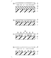
- the pattern forming method of the second aspect of the present invention comprises a step of forming a photocurable film on a substrate using the photocurable composition of the first aspect (hereinafter referred to as “step (i)”). a step of pressing a mold having an uneven pattern against the photocurable film to transfer the uneven pattern to the photocurable film (hereinafter referred to as “step (ii)”); a step of exposing the photocurable film having the uneven pattern transferred thereto to form a cured film (hereinafter referred to as “step (iii)”) while pressing against the flexible film; and peeling the mold from the cured film. and a step (hereinafter referred to as “step (iv)”).
- FIG. 1 is a schematic process diagram explaining one embodiment of the pattern forming method.
- step (i) a photocurable film is formed on a substrate using the photocurable composition of the first aspect described above.
- a substrate 1 is coated with the photocurable composition of the first aspect described above to form a photocurable film 2 .
- the mold 3 is arranged above the photocurable film 2 .
- the substrate 1 can be selected according to various uses, and examples thereof include substrates for electronic components, substrates having predetermined wiring patterns formed thereon, and the like. More specifically, metal substrates such as silicon, silicon nitride, copper, chromium, iron, and aluminum, glass substrates, and the like are included. Materials for the wiring pattern include, for example, copper, aluminum, nickel, and gold. Further, the shape of the substrate 1 is not particularly limited, and may be plate-like or roll-like. Further, as the substrate 1, a light-transmitting or non-light-transmitting substrate can be selected depending on the combination with the mold.
- Examples of methods for applying the photocurable composition to the substrate 1 include spin coating, spraying, ink jetting, roll coating, spin coating, and the like. Since the photocurable film 2 functions as a mask in the etching process of the substrate 1 that may be performed later, it is preferable that the film thickness when applied to the substrate 1 is uniform. From this point of view, the spin coating method is suitable for applying the photocurable composition to the substrate 1 .
- the film thickness of the photocurable film 2 may be appropriately selected depending on the application, and may be, for example, about 0.05 to 30 ⁇ m.
- step (ii) a mold having an uneven pattern is pressed against the photocurable film to transfer the uneven pattern to the photocurable film.
- a mold 3 having a fine uneven pattern on the surface thereof is pressed against the substrate 1 on which the photocurable film 2 is formed so as to face the photocurable film 2 .
- the photocurable film 2 is deformed according to the concave-convex structure of the mold 3 .
- the pressure on the photocurable film 2 when the mold 3 is pressed is preferably 10 MPa or less, more preferably 5 MPa or less, and particularly preferably 1 MPa or less.
- the concave-convex pattern of the mold 3 can be formed according to desired processing accuracy by photolithography, electron beam drawing, or the like, for example.
- the mold 3 is preferably a light transmissive mold.
- the material of the light-transmitting mold is not particularly limited as long as it has predetermined strength and durability. Specific examples include glass, quartz, light-transparent resin films such as polymethyl methacrylate and polycarbonate resin, transparent metal deposition films, flexible films such as polydimethylsiloxane, photocured films, metal films, and the like.
- Step (iii) In the step (iii), while pressing the mold against the photocurable film, the photocurable film having the uneven pattern transferred thereto is exposed to light to form a cured resin film.
- the photocurable film 2 onto which the uneven pattern has been transferred is exposed to light.
- the photocurable film 2 is irradiated with electromagnetic waves such as ultraviolet rays (UV). Due to the exposure, the photocurable film 2 is cured while the mold 3 is pressed, and a cured film (cured pattern) is formed on which the uneven pattern of the mold 3 is transferred.
- the mold 3 in FIG. 1C has transparency to electromagnetic waves.
- the light used to cure the photocurable film 2 is not particularly limited, and examples thereof include light or radiation with wavelengths in the regions of high-energy ionizing radiation, near-ultraviolet rays, far-ultraviolet rays, visible rays, and infrared rays.
- the radiation for example, microwaves, EUV, LED, semiconductor laser light, or laser light used in semiconductor microfabrication, such as 248 nm KrF excimer laser light or 193 nm ArF excimer laser light, can be suitably used.
- Monochromatic light may be used for these lights, or light with different wavelengths (mixed light) may be used.
- step (iv) the mold is separated from the cured film. As shown in FIG. 1(D), the mold 3 is separated from the cured film. As a result, a pattern 2 ′ (cured pattern) made of a cured film to which the uneven pattern is transferred is patterned on the substrate 1 .
- a photocurable composition containing the above-described (X) component, (T) component, (B) component, and (C) component is used. Since such a photocurable composition is used, a pattern having a high refractive index and excellent light resistance can be formed.
- a release agent may be applied to the surface 31 of the mold 3 that is in contact with the photocurable film 2 (FIG. 1(A)).
- release agents here include silicone-based release agents, fluorine-based release agents, polyethylene-based release agents, polypropylene-based release agents, paraffin-based release agents, montan-based release agents, and carnauba-based release agents. stencil agents and the like.
- fluorine-based release agents are preferred.
- a commercially available coating-type release agent such as OPTOOL DSX manufactured by Daikin Industries, Ltd. can be suitably used.
- the release agent may be used alone or in combination of two or more.
- an organic layer may be provided between the substrate 1 and the photocurable film 2 . Accordingly, by etching the substrate 1 using the photocurable film 2 and the organic layer as a mask, a desired pattern can be easily and reliably formed on the substrate 1 .
- the film thickness of the organic layer may be appropriately adjusted according to the depth of processing (etching) of the substrate 1, and is preferably 0.02 to 2.0 ⁇ m, for example.
- the material of the organic layer preferably has lower etching resistance to oxygen-based gas than the photocurable composition and higher etching resistance to halogen-based gas than the substrate 1 .
- a method for forming the organic layer is not particularly limited, but examples thereof include a sputtering method and a spin coating method.
- the pattern forming method of the second aspect may further include other steps (optional steps) in addition to steps (i) to (iv).
- steps (optional steps) include an etching step (step (v)) and a step of removing a cured film (cured pattern) after etching treatment (step (vi)).
- step (v) for example, the substrate 1 is etched using the pattern 2' obtained in the above steps (i) to (iv) as a mask.
- the substrate 1 on which the pattern 2' is formed is irradiated with at least one of plasma and reactive ions (indicated by arrows), thereby exposing the substrate to the pattern 2' side.
- One portion is removed by etching to a predetermined depth.
- the plasma or reactive ion gas used in step (v) is not particularly limited as long as it is a gas commonly used in the field of dry etching.
- step (vi) the cured film remaining after the etching treatment in step (v) is removed. As shown in FIG. 2F, this is a step of removing the cured film (pattern 2') remaining on the substrate 1 after the substrate 1 has been etched.
- a method for removing the cured film (pattern 2′) remaining on the substrate 1 is not particularly limited, but an example thereof includes a process of washing the substrate 1 using a solution that dissolves the cured film.
- ⁇ (X) component (metal oxide nanoparticles) (X)-1: Titania particles, manufactured by Tayca Corporation, product name "NS405". Volume average primary particle diameter 15 nm. (X)-2: Titania particles, manufactured by Ishihara Sangyo Co., Ltd., product name "LDB-014-35". Volume average primary particle diameter 15 nm. (X)-3: Zirconia particles, manufactured by Daiichi Kigenso Kagaku Kogyo Co., Ltd., product name “UEP-100”. Volume average primary particle diameter 15 nm.
- B component (photopolymerizable monomer)
- B)-1 Polyfunctional acrylate, manufactured by Nippon Kayaku Co., Ltd., product name "KAYARAD DPHA”.
- B)-2 Trimethylolpropane triacrylate, manufactured by Kyoeisha Chemical Co., Ltd., product name "Light acrylate TMP-A”.
- (C) component (photopolymerizable sulfur compound) (C)-1: Bis(4-methacryloylthiophenyl) sulfide, manufactured by Tokyo Chemical Industry Co., Ltd.
- ⁇ (Z) component (photopolymerizable aromatic compound) (Z)-1 Bisphenol A type epoxy acrylate, manufactured by Shin-Nakamura Chemical Co., Ltd., product name "NK Oligo EA-1010NT2".
- (Z)-2 p-phenylbenzyl acrylate, manufactured by Shin-Nakamura Chemical Co., Ltd., product name "NK Ester A-BPML”.
- the photocurable composition was adjusted to a film thickness of 600 nm and spin-coated onto a silicon substrate. Next, pre-baking is performed at 100° C. for 1 minute, and transfer is performed using an imprinting apparatus ST-200 manufactured by Toshiba Machine Co., Ltd. at a transfer pressure of 0.5 MPa, a transfer time of 30 seconds, and an exposure amount of 1 J/cm 2 (in a vacuum atmosphere of 200 Pa). A test was conducted, and the transferability of the fine pattern and the filling property were evaluated according to the following criteria. A standard film mold LSP70-140 (70 nm Line & Space) manufactured by Soken Kagaku Co., Ltd. was used as the mold. Good: 95% or more (when confirmed by SEM, the mold is 100% filled and the pattern is transferred) Bad: less than 95%
- the photocurable composition was adjusted to a film thickness of 600 nm and spin-coated onto a silicon substrate. Next, pre-baking was performed at 100° C. for 1 minute, and photo-curing treatment was performed with an exposure amount of 1 J/cm 2 (in a vacuum atmosphere of 200 Pa) using an imprinting apparatus ST-200 manufactured by Toshiba Machine Co., Ltd. to obtain a cured film. The resulting cured film was described in J. Am. A.
- the refractive index at a wavelength of 530 nm was measured using a spectroscopic ellipsometer M2000 manufactured by Woollam.
- the photocurable compositions of Examples 1 to 13 to which the present invention is applied have good imprintability and a refractive index of 1.86 or more, and have a high refractive index.
- the photocurable compositions of Comparative Examples 1, 3 to 5, 11 and 12 had good imprintability, but had a refractive index of 1.85 or less.
- the photocurable compositions of Comparative Examples 2, 6 to 10 and 13 to 15 had a refractive index of 1.86 or more, but had poor imprintability. From these results, it was confirmed that the photocurable compositions of Examples had good imprintability and provided cured resin films having a high refractive index.
Landscapes
- Chemical & Material Sciences (AREA)
- Health & Medical Sciences (AREA)
- Chemical Kinetics & Catalysis (AREA)
- Medicinal Chemistry (AREA)
- Polymers & Plastics (AREA)
- Organic Chemistry (AREA)
- Physics & Mathematics (AREA)
- General Physics & Mathematics (AREA)
- Engineering & Computer Science (AREA)
- Ceramic Engineering (AREA)
- Spectroscopy & Molecular Physics (AREA)
- Polymerisation Methods In General (AREA)
Priority Applications (4)
| Application Number | Priority Date | Filing Date | Title |
|---|---|---|---|
| CN202280021336.9A CN116981700A (zh) | 2021-03-16 | 2022-03-07 | 光固化性组合物及图案形成方法 |
| US18/550,002 US20240166779A1 (en) | 2021-03-16 | 2022-03-07 | Photocurable composition and pattern formation method |
| EP22771162.9A EP4310104A4 (en) | 2021-03-16 | 2022-03-07 | PHOTOCURABLE COMPOSITION AND PATTERN FORMING METHOD |
| JP2023506980A JPWO2022196408A1 (https=) | 2021-03-16 | 2022-03-07 |
Applications Claiming Priority (2)
| Application Number | Priority Date | Filing Date | Title |
|---|---|---|---|
| JP2021-042612 | 2021-03-16 | ||
| JP2021042612 | 2021-03-16 |
Publications (1)
| Publication Number | Publication Date |
|---|---|
| WO2022196408A1 true WO2022196408A1 (ja) | 2022-09-22 |
Family
ID=83320423
Family Applications (1)
| Application Number | Title | Priority Date | Filing Date |
|---|---|---|---|
| PCT/JP2022/009681 Ceased WO2022196408A1 (ja) | 2021-03-16 | 2022-03-07 | 光硬化性組成物及びパターン形成方法 |
Country Status (5)
| Country | Link |
|---|---|
| US (1) | US20240166779A1 (https=) |
| EP (1) | EP4310104A4 (https=) |
| JP (1) | JPWO2022196408A1 (https=) |
| CN (1) | CN116981700A (https=) |
| WO (1) | WO2022196408A1 (https=) |
Citations (11)
| Publication number | Priority date | Publication date | Assignee | Title |
|---|---|---|---|---|
| JP2003318313A (ja) * | 2002-04-24 | 2003-11-07 | Toray Ind Inc | セラミックス基板の製造方法 |
| JP2004176006A (ja) * | 2002-11-29 | 2004-06-24 | Sumitomo Seika Chem Co Ltd | 光硬化性組成物 |
| JP2008105414A (ja) * | 2006-09-27 | 2008-05-08 | Fujifilm Corp | 光ナノインプリントリソグラフィ用硬化性組成物およびそれを用いたパターン形成方法 |
| JP2009102550A (ja) * | 2007-10-24 | 2009-05-14 | Mitsubishi Chemicals Corp | 重合性組成物およびその硬化物 |
| JP2011187824A (ja) * | 2010-03-10 | 2011-09-22 | Fujifilm Corp | 微細パターン製造方法、微細パターン付き基板、微細パターン付き基板を含む光源装置および画像表示装置 |
| JP2012216655A (ja) * | 2011-03-31 | 2012-11-08 | Jsr Corp | ナノインプリント用感放射線性組成物、及びパターン形成方法 |
| JP2013095833A (ja) | 2011-10-31 | 2013-05-20 | Nissan Chem Ind Ltd | 高屈折率インプリント材料 |
| JP2013191800A (ja) | 2012-03-15 | 2013-09-26 | Tokyo Ohka Kogyo Co Ltd | 光インプリント用の膜形成組成物及び光学部材の製造方法 |
| JP2020132760A (ja) * | 2019-02-19 | 2020-08-31 | オーウエル株式会社 | 光硬化性組成物、硬化物、及びレンズ |
| JP2021031669A (ja) * | 2019-08-28 | 2021-03-01 | 東京応化工業株式会社 | 硬化性インク組成物、硬化物、及びナノコンポジット |
| JP2021042612A (ja) | 2019-09-12 | 2021-03-18 | 株式会社流機エンジニアリング | トンネル工事用装置およびトンネル工事方法 |
Family Cites Families (1)
| Publication number | Priority date | Publication date | Assignee | Title |
|---|---|---|---|---|
| US20190233556A1 (en) * | 2016-10-21 | 2019-08-01 | Corning Incorporated | High refractive index polymerizable monomers and applications thereof |
-
2022
- 2022-03-07 EP EP22771162.9A patent/EP4310104A4/en active Pending
- 2022-03-07 CN CN202280021336.9A patent/CN116981700A/zh active Pending
- 2022-03-07 WO PCT/JP2022/009681 patent/WO2022196408A1/ja not_active Ceased
- 2022-03-07 JP JP2023506980A patent/JPWO2022196408A1/ja active Pending
- 2022-03-07 US US18/550,002 patent/US20240166779A1/en active Pending
Patent Citations (11)
| Publication number | Priority date | Publication date | Assignee | Title |
|---|---|---|---|---|
| JP2003318313A (ja) * | 2002-04-24 | 2003-11-07 | Toray Ind Inc | セラミックス基板の製造方法 |
| JP2004176006A (ja) * | 2002-11-29 | 2004-06-24 | Sumitomo Seika Chem Co Ltd | 光硬化性組成物 |
| JP2008105414A (ja) * | 2006-09-27 | 2008-05-08 | Fujifilm Corp | 光ナノインプリントリソグラフィ用硬化性組成物およびそれを用いたパターン形成方法 |
| JP2009102550A (ja) * | 2007-10-24 | 2009-05-14 | Mitsubishi Chemicals Corp | 重合性組成物およびその硬化物 |
| JP2011187824A (ja) * | 2010-03-10 | 2011-09-22 | Fujifilm Corp | 微細パターン製造方法、微細パターン付き基板、微細パターン付き基板を含む光源装置および画像表示装置 |
| JP2012216655A (ja) * | 2011-03-31 | 2012-11-08 | Jsr Corp | ナノインプリント用感放射線性組成物、及びパターン形成方法 |
| JP2013095833A (ja) | 2011-10-31 | 2013-05-20 | Nissan Chem Ind Ltd | 高屈折率インプリント材料 |
| JP2013191800A (ja) | 2012-03-15 | 2013-09-26 | Tokyo Ohka Kogyo Co Ltd | 光インプリント用の膜形成組成物及び光学部材の製造方法 |
| JP2020132760A (ja) * | 2019-02-19 | 2020-08-31 | オーウエル株式会社 | 光硬化性組成物、硬化物、及びレンズ |
| JP2021031669A (ja) * | 2019-08-28 | 2021-03-01 | 東京応化工業株式会社 | 硬化性インク組成物、硬化物、及びナノコンポジット |
| JP2021042612A (ja) | 2019-09-12 | 2021-03-18 | 株式会社流機エンジニアリング | トンネル工事用装置およびトンネル工事方法 |
Non-Patent Citations (1)
| Title |
|---|
| See also references of EP4310104A4 |
Also Published As
| Publication number | Publication date |
|---|---|
| EP4310104A4 (en) | 2025-04-23 |
| EP4310104A1 (en) | 2024-01-24 |
| JPWO2022196408A1 (https=) | 2022-09-22 |
| US20240166779A1 (en) | 2024-05-23 |
| CN116981700A (zh) | 2023-10-31 |
Similar Documents
| Publication | Publication Date | Title |
|---|---|---|
| JP6029558B2 (ja) | 光インプリント用硬化性組成物、パターン形成方法、微細パターン、および半導体デバイスの製造方法 | |
| US20220334475A1 (en) | Photocurable composition and pattern forming method | |
| JP2010000612A (ja) | ナノインプリント用硬化性組成物、パターン形成方法 | |
| JP2009206197A (ja) | ナノインプリント用硬化性組成物、硬化物およびその製造方法 | |
| WO2013136858A1 (ja) | 光インプリント用硬化性組成物、パターン形成方法およびパターン | |
| JP2010013514A (ja) | ナノインプリント用硬化性組成物、これを用いた硬化物、並びに、液晶表示装置用部材 | |
| WO2014050855A1 (ja) | 光インプリント用硬化性組成物、パターン形成方法、微細パターンおよび半導体デバイスの製造方法 | |
| WO2009110536A1 (ja) | ナノインプリント用硬化性組成物、これを用いた硬化物およびその製造方法、並びに、液晶表示装置用部材 | |
| JP7175092B2 (ja) | 光硬化性組成物及びパターン形成方法 | |
| JP6338061B2 (ja) | 低離型力性を有するインプリント材料 | |
| US20220347913A1 (en) | Pattern forming method and method of producing curable composition | |
| WO2023145534A1 (ja) | ナノインプリント用組成物及びパターン形成方法 | |
| JP7458909B2 (ja) | 光硬化性組成物及びパターン形成方法 | |
| US12523930B2 (en) | Nanoimprint composition and pattern forming method | |
| JP2009206196A (ja) | ナノインプリント用硬化性組成物、これを用いた硬化物およびその製造方法、並びに、液晶表示装置用部材 | |
| US20240166779A1 (en) | Photocurable composition and pattern formation method | |
| US20240158541A1 (en) | Photocurable composition and pattern-forming method | |
| WO2022230871A1 (ja) | 硬化性組成物及びパターン形成方法 | |
| US20220373889A1 (en) | Pattern forming method | |
| JP7535931B2 (ja) | 光硬化性組成物及びパターン形成方法 | |
| JP2010083970A (ja) | ナノインプリント用硬化性組成物、硬化物およびその製造方法 |
Legal Events
| Date | Code | Title | Description |
|---|---|---|---|
| 121 | Ep: the epo has been informed by wipo that ep was designated in this application |
Ref document number: 22771162 Country of ref document: EP Kind code of ref document: A1 |
|
| ENP | Entry into the national phase |
Ref document number: 2023506980 Country of ref document: JP Kind code of ref document: A |
|
| WWE | Wipo information: entry into national phase |
Ref document number: 18550002 Country of ref document: US |
|
| WWE | Wipo information: entry into national phase |
Ref document number: 202280021336.9 Country of ref document: CN |
|
| WWE | Wipo information: entry into national phase |
Ref document number: 2022771162 Country of ref document: EP |
|
| NENP | Non-entry into the national phase |
Ref country code: DE |
|
| ENP | Entry into the national phase |
Ref document number: 2022771162 Country of ref document: EP Effective date: 20231016 |