WO2022168826A1 - 圧電素子、圧電装置、および圧電素子の製造方法 - Google Patents
圧電素子、圧電装置、および圧電素子の製造方法 Download PDFInfo
- Publication number
- WO2022168826A1 WO2022168826A1 PCT/JP2022/003806 JP2022003806W WO2022168826A1 WO 2022168826 A1 WO2022168826 A1 WO 2022168826A1 JP 2022003806 W JP2022003806 W JP 2022003806W WO 2022168826 A1 WO2022168826 A1 WO 2022168826A1
- Authority
- WO
- WIPO (PCT)
- Prior art keywords
- region
- piezoelectric element
- piezoelectric
- film
- support
- Prior art date
- Legal status (The legal status is an assumption and is not a legal conclusion. Google has not performed a legal analysis and makes no representation as to the accuracy of the status listed.)
- Ceased
Links
Images


Classifications
-
- H—ELECTRICITY
- H10—SEMICONDUCTOR DEVICES; ELECTRIC SOLID-STATE DEVICES NOT OTHERWISE PROVIDED FOR
- H10N—ELECTRIC SOLID-STATE DEVICES NOT OTHERWISE PROVIDED FOR
- H10N30/00—Piezoelectric or electrostrictive devices
- H10N30/704—Piezoelectric or electrostrictive devices based on piezoelectric or electrostrictive films or coatings
- H10N30/706—Piezoelectric or electrostrictive devices based on piezoelectric or electrostrictive films or coatings characterised by the underlying bases, e.g. substrates
- H10N30/708—Intermediate layers, e.g. barrier, adhesion or growth control buffer layers
-
- H—ELECTRICITY
- H10—SEMICONDUCTOR DEVICES; ELECTRIC SOLID-STATE DEVICES NOT OTHERWISE PROVIDED FOR
- H10N—ELECTRIC SOLID-STATE DEVICES NOT OTHERWISE PROVIDED FOR
- H10N30/00—Piezoelectric or electrostrictive devices
- H10N30/30—Piezoelectric or electrostrictive devices with mechanical input and electrical output, e.g. functioning as generators or sensors
- H10N30/308—Membrane type
-
- H—ELECTRICITY
- H04—ELECTRIC COMMUNICATION TECHNIQUE
- H04R—LOUDSPEAKERS, MICROPHONES, GRAMOPHONE PICK-UPS OR LIKE ACOUSTIC ELECTROMECHANICAL TRANSDUCERS; ELECTRIC HEARING AIDS; PUBLIC ADDRESS SYSTEMS
- H04R1/00—Details of transducers, loudspeakers or microphones
- H04R1/02—Casings; Cabinets ; Supports therefor; Mountings therein
-
- H—ELECTRICITY
- H04—ELECTRIC COMMUNICATION TECHNIQUE
- H04R—LOUDSPEAKERS, MICROPHONES, GRAMOPHONE PICK-UPS OR LIKE ACOUSTIC ELECTROMECHANICAL TRANSDUCERS; ELECTRIC HEARING AIDS; PUBLIC ADDRESS SYSTEMS
- H04R17/00—Piezoelectric transducers; Electrostrictive transducers
- H04R17/02—Microphones
-
- H—ELECTRICITY
- H10—SEMICONDUCTOR DEVICES; ELECTRIC SOLID-STATE DEVICES NOT OTHERWISE PROVIDED FOR
- H10N—ELECTRIC SOLID-STATE DEVICES NOT OTHERWISE PROVIDED FOR
- H10N30/00—Piezoelectric or electrostrictive devices
- H10N30/01—Manufacture or treatment
- H10N30/07—Forming of piezoelectric or electrostrictive parts or bodies on an electrical element or another base
- H10N30/074—Forming of piezoelectric or electrostrictive parts or bodies on an electrical element or another base by depositing piezoelectric or electrostrictive layers, e.g. aerosol or screen printing
-
- H—ELECTRICITY
- H10—SEMICONDUCTOR DEVICES; ELECTRIC SOLID-STATE DEVICES NOT OTHERWISE PROVIDED FOR
- H10N—ELECTRIC SOLID-STATE DEVICES NOT OTHERWISE PROVIDED FOR
- H10N30/00—Piezoelectric or electrostrictive devices
- H10N30/01—Manufacture or treatment
- H10N30/08—Shaping or machining of piezoelectric or electrostrictive bodies
- H10N30/082—Shaping or machining of piezoelectric or electrostrictive bodies by etching, e.g. lithography
-
- H—ELECTRICITY
- H10—SEMICONDUCTOR DEVICES; ELECTRIC SOLID-STATE DEVICES NOT OTHERWISE PROVIDED FOR
- H10N—ELECTRIC SOLID-STATE DEVICES NOT OTHERWISE PROVIDED FOR
- H10N30/00—Piezoelectric or electrostrictive devices
- H10N30/80—Constructional details
- H10N30/85—Piezoelectric or electrostrictive active materials
- H10N30/853—Ceramic compositions
Definitions
- the present disclosure relates to a piezoelectric element having a vibration region, a piezoelectric device, and a method of manufacturing the piezoelectric element.
- the vibration region of the piezoelectric element is configured to have a piezoelectric film and an electrode film connected to the piezoelectric film, and is cantilevered.
- the piezoelectric film deforms and charges are generated in the piezoelectric film. Therefore, the sound pressure applied to the vibration region is detected by taking out the charges generated in the piezoelectric film through the electrode film.
- An object of the present disclosure is to provide a piezoelectric element, a piezoelectric device, and a method of manufacturing the piezoelectric element that can improve detection accuracy.
- the piezoelectric element includes a support, a piezoelectric film disposed on the support, and an electrode film connected to the piezoelectric film and extracting charges generated by deformation of the piezoelectric film. and a vibrating portion that has a support region supported by a support and a vibration region that is connected to the support region and is floating from the support, and that outputs a pressure detection signal based on an electric charge; , and the vibration region has a plurality of slits formed from the support region side toward the center of the vibration region, and is in a state of being supported on both sides with respect to the support region.
- the resonance frequency can be increased compared to the case where the vibration region is supported by a cantilever. Therefore, it is possible to widen the range of frequencies for which the detection sensitivity can be maintained, and to improve the detection accuracy.
- a piezoelectric device includes the piezoelectric element described above, a mounted member on which the piezoelectric element is mounted, and a lid portion fixed to the mounted member while housing the piezoelectric element. and a casing in which a through hole communicating with the outside and through which pressure is introduced is formed.
- the manufacturing method for the piezoelectric element includes preparing a support, forming a piezoelectric film and an electrode film on the support, and forming a piezoelectric film and an electrode film on the piezoelectric film and the electrode film.
- An etching mask material is provided, openings are formed in the etching mask material to expose portions of the piezoelectric film where the slits are to be formed, and etching is performed using the etching mask material as a mask to penetrate the piezoelectric film.
- a slit reaching the support is formed, and the side surface exposed from the slit is a vibration area constituting portion that becomes a tapered portion in which the width is narrowed from one side opposite to the support side toward the other side opposite to the one side. and forming a recess from the opposite side of the support to the piezoelectric film side to float the vibration region forming portion, thereby forming a vibrating portion having a vibration region, the piezoelectric film and
- the electrode film the piezoelectric film and the electrode film are formed so that only the piezoelectric film is exposed from the side surface when forming the vibration region forming part, and by forming the slit, the side surface and the side surface forming the tapered portion are formed. , slits are formed such that the angle between one surface and a parallel surface is 39 to 81°.
- FIG. 1C It is a manufacturing method of the piezoelectric element shown in FIG. 1C. It is a manufacturing method of a piezoelectric element continued from FIG. 4A. It is a manufacturing method of a piezoelectric element continued from FIG.
- FIG. 4B. 1 is a cross-sectional view of a piezoelectric device according to a first embodiment
- FIG. 4 is a diagram showing the relationship between the connection length and the resonance frequency of the piezoelectric element
- FIG. FIG. 4 is a diagram showing the relationship between the frequency applied to the vibrating region and the output signal
- It is a figure which shows the relationship between connection length and generated stress ratio.
- It is a figure which shows the relationship between a sound pressure and an output signal.
- FIG. 5 is a plan view of a piezoelectric element in a modified example of the first embodiment
- FIG. 5 is a plan view of a piezoelectric element in a modified example of the first embodiment
- FIG. 5 is a plan view of a vibration region in a modified example of the first embodiment
- FIG. 5 is a plan view of a vibration region in a modified example of the first embodiment
- FIG. 5 is a plan view of a vibration region in a modified example of the first embodiment;
- FIG. 5 is a plan view of a vibration region in a modified example of the first embodiment;
- FIG. 5 is a plan view of a vibration region in a modified example of the first embodiment;
- FIG. 5 is a plan view of a vibration region in a modified example of the first embodiment;
- FIG. 5 is a plan view of a vibration region in a modified example of the first embodiment;
- FIG. 5 is a plan view of a vibration region in a modified example of the first embodiment;
- FIG. 8 is a plan view of an electrode film formed in a first region in a modified example of the first embodiment;
- 13 is a schematic circuit diagram of the piezoelectric element having the electrode film shown in FIG. 12.
- FIG. 8 is a plan view of a piezoelectric element in a second embodiment
- FIG. 11 is a schematic diagram of a vibration region described in a third embodiment
- FIG. 4 is a schematic diagram showing the magnitude of bending moment in a vibration region
- FIG. 4 is a diagram showing stress distribution in a vibration region
- FIG. 11 is a plan view of a piezoelectric element in a third embodiment
- 19 is a schematic circuit diagram of the piezoelectric element shown in FIG. 18.
- FIG. FIG. 11 is a cross-sectional view of a piezoelectric element in a fourth embodiment
- 21 is a plan view of the piezoelectric element shown in FIG. 20;
- FIG. 11 is a cross-sectional view of a piezoelectric element in a fifth embodiment;
- FIG. 23 is a plan view of the piezoelectric element shown in FIG. 22;
- FIG. 11 is a plan view of a piezoelectric element in a sixth embodiment;
- FIG. 14 is a plan view of an electrode film formed in a first region in the sixth embodiment;
- FIG. 11 is a schematic circuit diagram of a piezoelectric element in a sixth embodiment;
- FIG. 11 is a cross-sectional view of a piezoelectric element in a sixth embodiment;
- FIG. 11 is a plan view of a piezoelectric element in a modified example of the sixth embodiment;
- FIG. 14 is a plan view of an electrode film formed in a first region in a modified example of the sixth embodiment;
- FIG. 11 is a schematic circuit diagram of a piezoelectric element in a modified example of the sixth embodiment;
- FIG. 11 is a plan view of a piezoelectric element in a seventh embodiment;
- FIG. 11 is a cross-sectional view of a piezoelectric device according to a seventh embodiment; It is a cross-sectional schematic diagram of the piezoelectric device in 8th Embodiment.
- FIG. 5 is a diagram showing the relationship between slit width, slit length, and acoustic resistance when the thickness of the vibration region is constant.
- FIG. 5 is a diagram showing the relationship between the thickness of the vibration region, the slit length, and the acoustic resistance when the slit width is constant.
- FIG. 4 is a diagram showing the relationship between slit length and acoustic resistance ratio;
- FIG. 21 is a cross-sectional view of a slit of a piezoelectric element in a ninth embodiment;
- FIG. 5 is a diagram showing the relationship between the slit width on one side and the acoustic resistance;
- FIG. 21 is a cross-sectional view of a slit of a piezoelectric element in a modified example of the ninth embodiment;
- FIG. 21 is a cross-sectional view of a slit of a piezoelectric element in a modified example of the ninth embodiment;
- FIG. 21 is a cross-sectional view of a slit of a piezoelectric element in a modified example of the ninth embodiment;
- FIG. 22 is a plan view showing the positional relationship between the piezoelectric element and the joining member in the tenth embodiment;
- FIG. 22 is a plan view showing the positional relationship between the piezoelectric element and the joining member in the modified example of the tenth embodiment;
- FIG. 22 is a plan view showing the positional relationship between the piezoelectric element and the joining member in the modified example of the tenth embodiment;
- FIG. 22 is a plan view showing the positional relationship between the piezoelectric element and the joining member in the modified example of the tenth embodiment;
- FIG. 22 is a plan view showing the positional relationship between the piezoelectric element and the joining member in the modified example of the tenth embodiment;
- FIG. 22 is a plan view showing the positional relationship between the piezoelectric element and the joining member in the modified example of the tenth embodiment;
- FIG. 22 is a plan view showing the positional relationship between the piezoelectric element and the joining member in the modified example of the tenth embodiment;
- FIG. 21 is a cross-sectional view of a piezoelectric device according to an eleventh embodiment;
- FIG. 21 is a cross-sectional view of a piezoelectric element in a twelfth embodiment;
- FIG. 44 is a cross-sectional view showing a manufacturing process of the piezoelectric element shown in FIG. 43;
- FIG. 44B is a cross-sectional view showing the manufacturing process of the piezoelectric element continued from FIG. 44A;
- FIG. 44B is a cross-sectional view showing the manufacturing process of the piezoelectric element continued from FIG. 44B;
- 44C is a schematic diagram of a portion where a slit is formed in the manufacturing process of FIG. 44C;
- FIG. It is a figure which shows the relationship between frequency, sensitivity, and effective width.
- FIG. 3 is a diagram showing the relationship between the film thickness of an etching mask material with respect to the film thickness of a piezoelectric film and the angle formed;
- FIG. 10 is a cross-sectional view of a piezoelectric device according to another embodiment;
- FIGS. 1A, 1B, 1C, 2A and 2B A piezoelectric element 1 of the first embodiment will be described with reference to FIGS. 1A, 1B, 1C, 2A and 2B.
- the piezoelectric element 1 of this embodiment is preferably used as a microphone, for example.
- 1A corresponds to a cross-sectional view along the IA-IA line in FIG. 2A
- FIG. 1B corresponds to a cross-sectional view along the IB-IB line in FIG. 2A
- FIG. 1C is a cross-sectional view of FIG. It corresponds to the cross-sectional view along the IC-IC line in the middle.
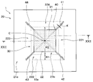
- FIG. 2A omits a first electrode portion 81, a second electrode portion 82, and the like, which will be described later. Also, in each figure corresponding to FIG. 2A described later, the first electrode portion 81, the second electrode portion 82, and the like are omitted as appropriate.
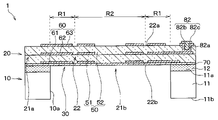
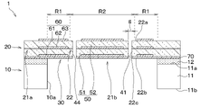
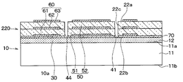
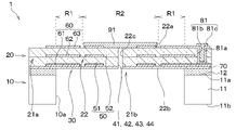
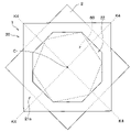
- the piezoelectric element 1 of this embodiment includes a support 10 and a vibrating portion 20, and has a rectangular planar shape.
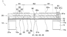
- the support 10 has a support substrate 11 having one surface 11 a and the other surface 11 b and an insulating film 12 formed on the one surface 11 a of the support substrate 11 .
- the support substrate 11 is made of, for example, a silicon substrate or the like, and the insulating film 12 is made of an oxide film or the like.
- the vibrating section 20 constitutes a sensing section 30 that outputs a pressure detection signal corresponding to sound pressure or the like as pressure, and is arranged on the support 10 .
- the support member 10 is formed with a recess 10a for floating the inner edge side of the vibrating portion 20.
- the vibrating portion 20 has a support region 21a arranged on the support 10 and a floating region 21b that is connected to the support region 21a and floats above the recess 10a.
- the opening end of the recess 10a of the present embodiment on the vibrating portion 20 side (hereinafter also simply referred to as the opening end of the recess 10a) has a planar rectangular shape. Therefore, the entire floating region 21b has a planar rectangular shape.
- a slit 40 is formed in the floating region 21b so as to penetrate the floating region 21b in the thickness direction.
- first to fourth slits 41 to 44 are formed in the floating region 21b.
- the first to fourth slits 41 to 44 extend from the respective corners of the planar rectangular floating region 21b toward the central portion C of the floating region 21b.
- the first to fourth slits 41 to 44 are formed so as not to reach the central portion C.
- the first to fourth slits 41 to 44 are formed so as to terminate on the support region 21a side of the central portion C. As shown in FIG. That is, the first to fourth slits 41 to 44 are formed so as not to divide the floating region 21b.
- the first to fourth slits 41 to 44 are formed so that the slit lengths L along the extension direction are equal. Furthermore, the first to fourth slits 41 to 44 of this embodiment have a constant slit width g along the thickness direction of the vibrating region 22 .
- the floating region 21b constitutes the vibrating region 22, and the vibrating region 22 is supported on both sides by the support region 21a.
- the slit width g of the first to fourth slits 41 to 44 is a direction perpendicular to the extending direction of the first to fourth slits 41 to 44 and is a direction along the surface direction of the vibration region 22. length.
- the slit width g of the first to fourth slits 41 to 44 is the distance between the side surfaces 22c of the vibration region 22 exposed by the first slits 41 to 44.
- the surface of the vibration region 22 opposite to the support 10 is defined as one surface 22a of the vibration region 22, and the surface of the vibration region 22 facing the support 10 is defined as the other surface 22b of the vibration region 22.
- the surfaces exposed from the first to fourth slits 41 to 44 in the vibrating region 22 are defined as side surfaces 22c of the vibrating region 22.
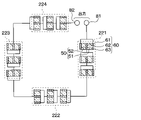
- the first to first regions are defined by one side forming the outer shape of the vibration region 22 and virtual lines K1 and K2 extending along the slits 41 to 44. These are referred to as fourth vibration regions 221-224.
- the normal line direction with respect to the one surface 22a of the vibration region 22 is simply called a normal line direction.
- the normal direction to the one surface 22a of the vibration region 22 in other words, when viewed from the normal direction to the one surface 22a of the vibration region 22.
- the virtual line extending along the first slit 41 and the third slit 43 is defined as a virtual line K1
- the virtual line extending along the second slit 42 and the fourth slit 44 is defined as a virtual line K2.
- a first vibration region 221 is defined as a region of the vibration region 22 that includes between the first slit 41 and the second slit 42 and is surrounded by the virtual lines K1 and K2.
- a second vibration region 222 includes a region between the second slit 42 and the third slit 43 in the vibration region 22 and is surrounded by the virtual lines K1 and K2.
- a third vibration region 223 includes a region between the third slit 43 and the fourth slit 44 in the normal direction and is surrounded by the virtual lines K1 and K2 in the vibration region 22 .
- a fourth vibration region 224 includes between the fourth slit 44 and the first slit 41 in the vibration region 22 and is surrounded by the virtual lines K1 and K2.
- the vibration region 22 of this embodiment is formed by integrating the first to fourth vibration regions 221 to 224 .
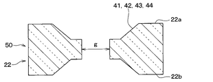
- the vibrating portion 20 has a piezoelectric film 50 and an electrode film 60 connected to the piezoelectric film 50 .
- the piezoelectric film 50 has a lower piezoelectric film 51 and an upper piezoelectric film 52 laminated on the lower piezoelectric film 51 .
- the electrode film 60 is arranged on the lower electrode film 61 arranged below the lower piezoelectric film 51 , the intermediate electrode film 62 arranged between the lower piezoelectric film 51 and the upper piezoelectric film 52 , and the upper piezoelectric film 52 . It has an upper layer electrode film 63 .
- the vibrating portion 20 has a bimorph structure in which the lower piezoelectric film 51 is sandwiched between the lower electrode film 61 and the intermediate electrode film 62, and the upper piezoelectric film 52 is sandwiched between the intermediate electrode film 62 and the upper electrode film 63. It is
- the lower piezoelectric film 51 and the upper piezoelectric film 52 are made of lead-free piezoelectric ceramics such as scandium aluminum nitride (ScAlN) and aluminum nitride (AlN).
- the lower electrode film 61, the intermediate electrode film 62, and the upper electrode film 63 are made of molybdenum, copper, platinum, platinum, titanium, or the like.
- the vibrating portion 20 of this embodiment has a base film 70 on which the lower piezoelectric film 51 and the lower electrode film 61 are arranged. That is, the piezoelectric film 50 and the electrode film 60 are arranged on the support 10 with the base film 70 interposed therebetween.
- the base film 70 is not necessarily required, but is provided to facilitate crystal growth when forming the lower layer piezoelectric film 51 and the like.
- the base film 70 is made of aluminum nitride or the like.
- the thickness of the piezoelectric film 50 is approximately 1 ⁇ m, and the thickness of the underlying film 70 is approximately several tens of nanometers. That is, the base film 70 is made extremely thin with respect to the piezoelectric film 50 .
- the portion on the side of the support region 21a that becomes the fixed end when the vibration region 22 vibrates is the first region R1, and the center portion C side is the second region R2.
- the lower electrode film 61, the intermediate electrode film 62, and the upper electrode film 63 are formed in the first region R1 and the second region R2, respectively.
- the lower electrode film 61, intermediate electrode film 62, and upper electrode film 63 formed in the first region R1 and the lower electrode film 61, intermediate electrode film 62, and upper electrode film 63 formed in the second region R2 are , are separated and insulated.
- the lower electrode film 61, the intermediate electrode film 62, and the upper electrode film 63 formed in the first region R1 are appropriately extended to the support region 21a.
- the lower electrode film 61, the intermediate electrode film 62, and the upper electrode film 63 are formed so as not to reach the first to fourth slits 41-44. That is, the lower electrode film 61, the intermediate electrode film 62, and the upper electrode film 63 are formed so as to terminate inside the side surface 22c exposed from the first to fourth slits 41 to 44 in the vibration region 22.
- the lower electrode film 61, the intermediate electrode film 62, and the upper electrode film 63 are arranged inside the first to fourth slits 41 to 44 in the normal direction. Therefore, the side surface 22 c of the vibration region 22 is composed of the lower piezoelectric film 51 , the upper piezoelectric film 52 and the underlying film 70 .
- first electrode portion 81 electrically connected to the lower electrode film 61 and the upper electrode film 63 formed in the first region R1, and an intermediate electrode portion 81 formed in the first region R1.
- a second electrode portion 82 electrically connected to the electrode film 62 is formed. As described above, the first electrode portion 81 and the second electrode portion 82 are omitted in FIG. 2A.
- the first electrode portion 81 is formed in a hole portion 81a passing through the upper layer electrode film 63, the upper layer piezoelectric film 52, and the lower layer piezoelectric film 51, and a through electrode 81b electrically connected to the lower layer electrode film 61 and the upper layer electrode film 63. have.
- the through electrode 81 b is electrically connected to the lower electrode film 61 and the upper electrode film 63 formed in the first vibration region 221 .
- the first electrode portion 81 also has a pad portion 81c formed on the through electrode 81b and electrically connected to the through electrode 81b.
- the second electrode portion 82 has a through electrode 82b that is formed in a hole portion 82a that penetrates the upper piezoelectric film 52 and exposes the intermediate electrode film 62, and that is electrically connected to the intermediate electrode film 62.
- the through electrode 82 b is electrically connected to the intermediate electrode film 62 formed in the fourth vibration region 224 .
- the second electrode portion 82 also has a pad portion 82c formed on the through electrode 82b and electrically connected to the through electrode 82b.
- the first electrode portion 81 and the second electrode portion 82 are made of molybdenum, copper, platinum, titanium, aluminum, or the like, like the electrode film 60 .
- the lower electrode film 61, the intermediate electrode film 62, and the upper electrode film 63 formed in the second region R2 are not electrically connected to the electrode portions 81 and 82, and are in a floating state. For this reason, the lower electrode film 61, the intermediate electrode film 62, and the upper electrode film 63 formed in the second region R2 are not necessarily required. It is provided to protect the portion located in the second region R2.
- the lower electrode film 61, the intermediate electrode film 62, and the upper electrode film 63 formed in the first region R1 are divided into first to fourth vibration regions 221-224. That is, the lower electrode film 61, the intermediate electrode film 62, and the upper electrode film 63 formed in the first region R1 are not formed so as to straddle the first to fourth vibration regions 221-224.
- the lower electrode film 61, the intermediate electrode film 62, and the upper electrode film 63 formed in the first region R1 of each of the vibration regions 221 to 224 are connected via wiring films (not shown) or the like.
- the lower electrode film 61, the intermediate electrode film 62, and the upper electrode film 63 of this embodiment are formed to be equal, and in this embodiment, they are rectangular in plan.
- the lower electrode film 61, the intermediate electrode film 62, and the upper electrode film 63 are divided into the first to fourth vibration regions 221 to 224 as described above. Therefore, the external shapes of the portions of the lower electrode film 61, the intermediate electrode film 62, and the upper electrode film 63 formed in the first region R1 here refer to the shapes of the lower electrode film 61, the intermediate electrode film 62, and the upper electrode film 63. It is a shape composed of the contour line of the portion located in the first region R1 in and the extension line of the contour line.
- the electrode film 60 formed in the first region R1 is hatched for easy understanding. Furthermore, although the electrode film 60 is shown in FIG. 2B, the lower electrode film 61, the intermediate electrode film 62, and the upper electrode film 63 that become the electrode film 60 are the same as the electrode film 60 in FIG. 2B in the first region R1. It has the same shape.
- the piezoelectric element 1 of this embodiment is configured to output changes in charge in the first to fourth vibration regions 221 to 224 as one pressure detection signal.
- each of the vibration regions 221 to 224 has a bimorph structure, and as shown in FIG. While the electrode films 63 are connected in parallel, the vibration regions 22 are connected in series. Then, the piezoelectric element 1 outputs the potential difference between the first electrode portion 81 and the second electrode portion 82 as a pressure detection signal.
- the second electrode portion 82 is connected to the ground, and the piezoelectric element 1 outputs the potential difference between the ground and the first electrode portion 81 as the pressure detection signal.
- FIGS. 4A, 4B, and 4C are sectional views of the portion corresponding to FIG. 1C.
- a base film 70, a piezoelectric film 50, an electrode film 60, a first electrode portion 81, a second electrode portion 82, and the like are formed on a support 10 having a support substrate 11 and an insulating film 12.
- a support 10 having a support substrate 11 and an insulating film 12.
- the piezoelectric element 1 shown in FIG. 1C without the recess 10a and the first to fourth slits 41 to 44 is prepared.
- the first electrode portion 81 and the second electrode portion 82 are formed in a different cross section from that in FIG. 4A.
- the base film 70, the piezoelectric film 50, the electrode film 60, and the like are formed by appropriately performing general sputtering, etching, or the like.
- the linear expansion coefficients of the base film 70 and the lower electrode film 61 support the base film 70 and the lower electrode film 61 . Since it is larger than the linear expansion coefficient of the body 10, it is formed in a state in which tensile stress remains. Therefore, when the piezoelectric film 50 is formed as it is, the piezoelectric film 50 is likely to be formed with residual tensile stress caused by the tensile stress of the base film 70 and the lower electrode film 61 . If tensile stress remains in the piezoelectric film 50, the characteristics of the piezoelectric element 1 tend to fluctuate. Therefore, when forming the piezoelectric film 50, for example, it is preferable to do as follows.
- the voltage applied during sputtering is made larger than when forming the lower piezoelectric film 51, so that compressive stress is generated in the upper piezoelectric film 52. is preferred.
- the tensile stress of the lower piezoelectric film 51 and the compressive stress of the upper piezoelectric film 52 are offset, and the stress remaining inside the piezoelectric film 50 as a whole can be reduced.
- the upper piezoelectric film 52 may be formed by sputtering a plurality of times.
- a tensile stress is generated in the portion on the lower piezoelectric film 51 side, and a compressive stress is generated in the uppermost layer side portion opposite to the lower piezoelectric film 51.
- the stress remaining inside the piezoelectric film 50 may be reduced.
- a vibration region forming portion 220 that becomes the vibration region 22 is formed by forming a recess 10a, which will be described later.
- the second and third slits 43 and 44 are formed in a cross section different from that in FIG. 4B.
- the vibration region forming portion 220 is a portion that becomes the vibration region 22 by forming the concave portion 10a. Therefore, in the drawing, the one surface, the other surface, and the side surface of the vibration region forming portion 220 are given the same reference numerals as the one surface 22a, the other surface 22b, and the side surface 22c of the vibration region 22.
- etching is performed from the other surface 11b of the support substrate 11 so as to penetrate the insulating film 12 and reach the underlying film 70, thereby forming the recesses 10a.
- the insulating film 12 is removed by isotropic wet etching to form the concave portion 10a.
- the vibration region forming portion 220 is suspended from the support 10 to form the vibration region 22, and the piezoelectric element 1 shown in FIG. 1 is manufactured.
- a protective resist or the like covering the upper piezoelectric film 52 and the upper electrode film 63 may be placed to form the concave portion 10a.
- the protective resist is removed after the recess 10a is formed.
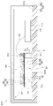
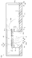
- the piezoelectric device of the present embodiment is constructed by housing a piezoelectric element 1 in a casing 100, as shown in FIG.
- the casing 100 includes a printed circuit board 101 on which the piezoelectric element 1 and a circuit board 110 that performs predetermined signal processing and the like are mounted, and a lid portion 102 fixed to the printed circuit board 101 so as to accommodate the piezoelectric element 1 and the circuit board 110 .
- the printed circuit board 101 corresponds to a mounted member.
- the printed circuit board 101 has wiring portions, through-hole electrodes, and the like formed as appropriate, and electronic components such as capacitors (not shown) are mounted as necessary.
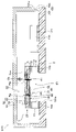
- the other surface 11b of the support substrate 11 of the piezoelectric element 1 is mounted on one surface 101a of the printed circuit board 101 via a bonding member 2 such as an adhesive.
- the circuit board 110 is mounted on one surface 101a of the printed circuit board 101 via a joint member 111 made of a conductive member.
- the pad portion 81 c of the piezoelectric element 1 and the circuit board 110 are electrically connected via bonding wires 120 .
- the pad portion 82c of the piezoelectric element 1 is electrically connected to the circuit board 110 via the bonding wire 120 in a cross section different from that in FIG.
- the lid portion 102 is made of metal, plastic, resin, or the like, and is fixed to the printed circuit board 101 via a bonding member such as an adhesive (not shown) so as to accommodate the piezoelectric element 1 and the circuit board 110 .
- a through hole 101b communicating with the external space is formed in a portion of the printed circuit board 101 that faces the sensing section 30 .
- the through-hole 101b has a substantially cylindrical shape, and is formed such that its central axis coincides with the central portion C of the vibration region 22 in the normal direction.
- a back space S2 includes a space located on the opposite side of the pressure receiving surface space S1 across the vibration region 22 and is continuous with the space without the slit 40 interposed therebetween.
- the back space S2 can be said to be a space in the casing 100 different from the pressure-receiving surface space S1, or a space excluding the pressure-receiving surface space S1.
- the pressure-receiving surface space S1 can also be said to be a space that affects pressing the surface of the vibration region 22 on the side of the through hole 101b formed in the casing 100 (that is, the other surface 22b in this embodiment).
- the back space S2 can also be said to be a space that affects pressing of the surface of the vibration region 22 opposite to the through hole 101b side (that is, one surface 22a in the present embodiment).
- the vibration region 22 vibrates. Charges are generated in the lower piezoelectric film 51 and the upper piezoelectric film 52 due to the stress corresponding to the displacement of the vibrating region 22 . Therefore, in such a piezoelectric device S ⁇ b>10 , sound pressure is detected by extracting the charges from the first electrode portion 81 and the second electrode portion 82 .
- the vibration region 22 is divided into the first region R1 where the stress tends to increase and the second region R2 where the stress tends to decrease.
- the lower electrode film 61, the upper electrode film 63, and the intermediate electrode film 62, which are arranged in the first region R1 are connected to the first and second electrode portions 81 and 82, and are connected to the first region R1. Electric charges generated in the lower piezoelectric film 51 and the upper piezoelectric film 52 located there are taken out. As a result, it is possible to suppress an increase in the influence of noise.
- the resonance frequency f of the vibration region 22 in the piezoelectric element 1 (hereinafter also simply referred to as the resonance frequency f of the piezoelectric element 1) is determined by the spring constant k of the vibration region 22 serving as a beam and the mass m of the vibration region 22. , and is expressed by Equation 1 below.
- the vibration region 22 has a double support structure to increase the spring constant k. Thereby, the resonance frequency f can be increased.
- the length between the first slit 41 and the center C of the vibration region 22 is defined as the first length X
- the length between the second slit 42 and the center C of the vibration region 22 is Let the length between them be the second length Y.
- the first length X and the second length Y are equal.
- the connection length that is, X+Y
- the resonance frequency f can be made higher than 20000 Hz (that is, 20 kHz), which is the audible range, by adjusting the connection length. In other words, by adjusting the connection length, the resonance frequency f will be able to exist. As a result, it is possible to widen the range of frequencies that can maintain the detection sensitivity.
- the thickness of the piezoelectric film 50 is about 1 ⁇ m, so when the connection length is about 300 ⁇ m, the resonance frequency f saturates at about 22.5 kHz.
- the frequency at which the detection sensitivity can be maintained can be broadened.
- This low-frequency roll-off frequency will be specifically described in an eighth embodiment, which will be described later.
- connection length is preferably adjusted according to the intended use.
- the generated stress ratio in FIG. 8 is based on the stress generated at the boundary between the vibration region 22 and the support region 21a when the vibration region 22 is cantilevered.
- the generated stress ratio indicates the ratio of the stress generated at the boundary between the vibration region 22 and the support region 21a when the vibration region 22 is supported on both sides with respect to the reference stress.
- the vibration regions 22 of the piezoelectric element 1 are supported on both sides. Therefore, compared to the case where the vibration region 22 is cantilevered, the resonance frequency f can be increased. Therefore, it is possible to widen the range of frequencies for which the detection sensitivity can be maintained, and to improve the detection accuracy.
- the resonance frequency f of the piezoelectric element 1 can be set to 20 kHz or higher. Therefore, in such a piezoelectric element 1, the resonance frequency f can be set outside the audible range, and the frequency that can maintain the detection sensitivity in the audible range can be widened.
- the linking length is preferably adjusted appropriately according to the application and the relationship with detection sensitivity.
- the slit lengths L of the first slit 41 and the third slit 43 and the second slit 42 and the fourth slit 44 may be different.
- the first length X and the second length Y may not be the same distance, and the first length X may be shorter than the second length Y. Also, although not shown, the first length X and the second length Y may be longer than the second length Y.
- first to fourth slits 41 to 44 may be formed only in the first region R1 in the vibration region 22, as shown in FIG. 10B. Also, although not shown, the first to fourth slits 41 to 44 may be formed to have different slit lengths L, respectively.
- the slit length L of the first to fourth slits 41 to 44 can be changed as appropriate, and can be changed according to the product to be mounted. Therefore, in the piezoelectric element 1 of this embodiment, it is possible to improve the selectivity of the product to be mounted.
- the planar shape of the vibration region 22 can be changed as appropriate.
- the vibration region 22 has a planar shape of hexagon, octagon, decagon, dodecagon, hexagon, hexagon, or circle. It may be shaped.
- the vibration region 22 may have another polygonal shape.
- the slits 40 formed in the vibrating regions 22 are omitted in FIGS. 11A to 11G, the slits 40 are formed in the vibrating regions 22, respectively.
- the planar shape of the vibrating region 22 is hexagonal as shown in FIG. 11A, six slits 40 are formed from each corner of the outer shape of the vibrating region 22 toward the central portion C. As shown in FIG.
- the plane shape of the vibration region 22 is circular as shown in FIG. 11G, a desired plurality of slits 40 are evenly formed in the circumferential direction.
- the electrode film 60 may be divided into a plurality of charge regions 60a in the first region R1.
- the electrode film 60 may be divided into three charge regions 60a in the first region R1 of each vibration region 221-224.
- the lower electrode film 61, the intermediate electrode film 62, and the upper electrode film 63, which form the electrode film 60 are each divided into charge regions 60a in the first region R1 as shown in FIG.
- the piezoelectric element 1 is in a state in which capacitances formed by the respective divided charge regions 60a are connected in series. According to this, the capacity in each vibration region 221 to 224 can be reduced, and the output can be improved. That is, it is possible to improve the detection sensitivity.
- the first to fourth slits 41 to 44 are tapered in the normal direction so that the slit width g is narrowed toward the central portion C. ing.
- the vibration region 22 is supported on both sides. Therefore, the resonance frequency f of the piezoelectric element 1 can be increased, and the same effects as those of the first embodiment can be obtained.
- the first to fourth slits 41 to 44 are tapered such that the slit width g narrows toward the central portion C of the vibration region 22 . Therefore, when sound pressure is applied to the vibrating region 22 and the vibrating region 22 bends, the slit widths g of the first to fourth slits 41 to 44 in the bent state can be easily made uniform. In other words, when the vibration region 22 is flexed, the slit widths g of the first to fourth slits 41 to 44 tend to be uniform between the support region 21a side portion and the center portion C side portion in the normal direction. Become. Therefore, it becomes difficult for differences in ease of local sound pressure release to occur in the first to fourth slits 41 to 44, and noise can be reduced. Therefore, it is possible to further improve the detection accuracy.
- a third embodiment will be described.
- the present embodiment is different from the first embodiment in how the first region R1 and the second region R2 are partitioned. Others are the same as those of the first embodiment, so description thereof is omitted here.
- the piezoelectric element 1 of this embodiment has the same configuration as that of the first embodiment, and the vibration regions 22 are supported on both sides.
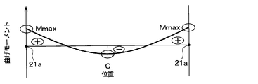
- FIG. 15 it is assumed that sound pressure is applied from the other surface 22b side of the vibration region 22.
- the maximum bending moment Mmax is generated in the vibration region 22 on the side of the support region 21a, and a large bending moment is also generated in the central portion C.
- FIG. 17 opposite stresses are generated in the lower piezoelectric film 51 and the upper piezoelectric film 52 .
- the central region 225 including the central portion C of the vibration region 22 and its peripheral portion is also the first region R1, and the charges in the central region 225 are also taken out.
- the center region 225 can also be said to be a region constituted by regions on the center portion C side of the first to fourth vibration regions 221 to 224 .
- the charges in the central region 225 are added to the charges in the first to fourth vibration regions 221 to 224 and output.
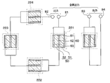
- a third electrode portion 83 and a fourth electrode portion 84 are formed in addition to the first electrode portion 81 and the second electrode portion 82 .
- the lower electrode film 61 and the upper electrode film 63 are electrically connected to the third electrode portion 83
- the intermediate electrode film 62 is connected to the fourth electrode portion 84 .
- the fourth electrode portion 82 connected to the intermediate electrode film 62 is connected to the ground, for example, similarly to the second electrode portion 82 .
- the piezoelectric element 1 detects the difference between the output based on the potential difference between the first electrode portion 81 and the second electrode portion 82 and the output based on the potential difference between the third electrode portion 83 and the fourth electrode portion 84 as a whole. Output as a pressure detection signal.
- the vibration region 22 is supported on both sides. Therefore, the resonance frequency f of the piezoelectric element 1 can be increased, and the same effects as those of the first embodiment can be obtained.
- the first to fourth slits 41 to 44 extend to the central portion C of the vibrating region 22.
- the first to fourth slits 41 to 44 are formed so as to intersect at the central portion C.
- the first to fourth vibration regions 221-224 are in a state of being partitioned by the first to fourth slits 41-44.
- 20 corresponds to a cross-sectional view taken along line XX-XX in FIG.
- FIG. 21 is not a cross-sectional view, a connecting member 90, which will be described later, is hatched for easy understanding.
- the connecting member 90 is embedded in the central portion C of the first to fourth slits 41 to 44 and its vicinity.
- the connecting member 90 integrates the first to fourth vibration regions 221 to 224, and the vibration region 22 is supported by the support region 21a.
- the connecting member 90 of the present embodiment is made of a material having a lower rigidity than the piezoelectric film 50, for example, a material obtained by mixing an ionic liquid with a polyimide component and hardening it by heat treatment at about 150.degree.
- the ionic liquid is a salt liquid compound composed only of ions (that is, anions and cations).
- Such a piezoelectric element 1 is manufactured, for example, as follows. That is, when forming the first to fourth slits 41 to 44 in the process of FIG. After that, a photoresist or the like is placed so as to cover the upper electrode film 63 and the like, and the photoresist is patterned so that an opening is formed in a portion where the connecting member 90 is to be placed. Next, the connecting members 90 are embedded in the first to fourth slits 41 to 44 by spin coating or the like, and are cured by heat treatment. Subsequently, by performing lift-off for removing the photoresist, the connecting members 90 are arranged in the first to fourth slits 41 to 44 . After that, the piezoelectric element 1 shown in FIGS. 20 and 21 is manufactured by performing the process of FIG. 4C.
- the vibration region 22 is supported on both sides. Therefore, the resonance frequency f of the piezoelectric element 1 can be increased, and the same effects as those of the first embodiment can be obtained.
- the connecting member 90 may support both sides of the vibration region 22 .
- the connecting member 90 is made of a material having lower rigidity than the piezoelectric film 50 . Therefore, it is possible to prevent the connecting member 90 from affecting the detection sensitivity of the piezoelectric element 1 .
- the connecting member 90 is not arranged in the first to fourth slits 41 to 44, and the connecting member 91 are placed.
- 22 corresponds to a cross-sectional view taken along line XXII--XXII in FIG.
- FIG. 23 is not a cross-sectional view, a connecting member 91, which will be described later, is hatched for easy understanding.
- the connecting member 91 is arranged on the one surface 22a of the vibration region 22 so as to cover (that is, straddle) the central portion C of the first to fourth slits 41 to 44 and the portions in the vicinity thereof. It is In this embodiment, the first to fourth vibration regions 221 to 224 are thus integrated, and the vibration region 22 is supported by the support region 21a.
- the connecting member 91 is made of a material having lower rigidity than the piezoelectric film 50, such as polyimide. More specifically, the connecting member 90 is made of polydimethylsiloxane (that is, PDMS) or the like.
- Such a piezoelectric element 1 is manufactured, for example, as follows. That is, after the first to fourth slits 41 to 44 are formed so as to intersect at the central portion C of the vibration region 22, the connecting member 91 is arranged by spin coating or the like. In this embodiment, the viscosity of the connecting member 91 is adjusted so that the connecting member 91 does not enter the first to fourth slits 41 to 44 when spin coating is performed. Subsequently, the connecting member 91 is patterned using a photoresist. Thereafter, the piezoelectric element 1 shown in FIGS. 22 and 23 is manufactured by performing the process of FIG. 4C.
- the vibration region 22 is supported on both sides. Therefore, the resonance frequency f of the piezoelectric element 1 can be increased, and the same effects as those of the first embodiment can be obtained.
- the connecting member 91 may support both sides of the vibration region 22 .
- the connecting member 91 is made of a material with lower rigidity than the piezoelectric film 50, the same effect as in the fourth embodiment can be obtained.
- the piezoelectric element 1 of this embodiment will be described with reference to FIGS. 24A and 24B. 22, the slit 40 is omitted. However, the slits 40 actually extend from each corner of the plane shape of the vibration region 22 toward the central portion C, as in the first embodiment.
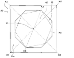
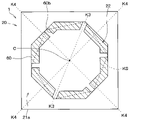
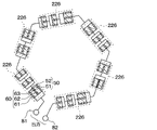
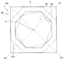
- the vibration region 22 has a regular octagonal outer shape in the normal direction.
- the shape of the opening of the concave portion 10a of the support 10 is a regular octagon.
- the support substrate 11 is made of silicon. Therefore, by making the shape of the opening of the recess 10a (that is, the outer shape of the vibration region 22) a regular octagonal shape, the opening end of the recess 10a (that is, the outer end of the vibration region 22) in the support substrate 11 is locally It is possible to suppress the concentration of strain at a location. Therefore, it is possible to suppress the concentration of strain on a local portion of the boundary between the vibration region 22 and the support region 21a.
- the electrode film 60 of the present embodiment has a regular octagonal external shape in the normal direction at the portion formed in the first region R1. That is, the electrode film 60 is formed so that the outer edge of the first region substantially coincides with the opening end of the recess 10a.
- the electrode film 60 is separated by an electrode film slit 60b that is different from the slit 40 in the portion formed in the first region R1.
- six electrode film slits 60b are formed, and a virtual shape (hereinafter also simply referred to as a virtual shape) KS formed by connecting predetermined locations in each of the electrode film slits 60b is a hexagon. It is formed to have a shape. More specifically, the electrode film slits 60b are formed so that a virtual shape KS formed by connecting the intersections of the electrode film slits 60b and the outer shape of the electrode film 60 is hexagonal.
- the outline of the portion of the electrode film 60 located in the first region R1 here means the outline of the portion of the electrode film 60 located in the first region R1 and the extension of the outline, as described above. Constructed shape.
- the electrode film 60 and the piezoelectric film 50 are arranged by stacking the lower electrode film 61, the lower piezoelectric film 51, the intermediate electrode film 62, the upper piezoelectric film 52, and the upper electrode film 63 in this order.
- the metal film is patterned into a desired shape by dry etching or the like using a mask. At this time, although a mask is used, there is a possibility that the underlying lower layer piezoelectric film 51 and upper layer piezoelectric film 52 will be etched.
- the piezoelectric film 50 when the piezoelectric film 50 is made of ScAlN, AlN, or the like, it has a hexagonal crystal structure. It is possible to prevent the crystallinity of the piezoelectric film 50 from collapsing. In other words, by matching the crystal structure of the piezoelectric film 50 to the portion where the electrode film slit 60b is formed, it is possible to suppress fluctuations in the characteristics of the piezoelectric film 50 .
- the piezoelectric element 1 of this embodiment As shown in FIG. 25, capacitances between the electrode films 61 to 63 are connected.
- the electrode film 60 is divided into six by the electrode film slits 60b different from the slits 40 . Therefore, the piezoelectric element 1 of this embodiment has six divided regions 226 and outputs a pressure detection signal based on the capacitance of each region 226 .
- the electrode films 60 of the present embodiment are separated by the electrode film slits 60 b as described above, and are not separated by the slits 40 . Therefore, as shown in FIG. 26, the electrode film 60 is in a continuous state at the portion where the slit 40 is formed.
- Such a piezoelectric element 1 is manufactured, for example, by forming the slit 40 or the electrode film slit 60b each time each film is formed when performing the steps of FIGS. 4A and 4B.
- a metal film is formed on the base film 70 .
- the electrode film slits 60b are formed.
- the lower piezoelectric film 51 is formed on the lower electrode film 61 , and the slit 40 penetrating only the lower piezoelectric film 51 is formed in the lower piezoelectric film 51 before forming the intermediate electrode film 62 .
- the intermediate electrode film 62, the upper layer piezoelectric film 52, and the upper layer electrode film 63 are similarly formed, thereby manufacturing the piezoelectric element 1 of the present embodiment.
- the outer edge on the side opposite to the central portion C is actually formed to the outside of the first region R1, and the inner edge is formed to the inside of the second region R2. It is Therefore, when forming the metal film and then patterning the metal film into a desired shape to form the intermediate electrode film 62 and the upper electrode film 63, the piezoelectric film 50 is removed in a portion different from the electrode film slit 60b. Even if it is removed, the piezoelectric film 50 outside the first region R1 is removed. Therefore, by making the virtual shape KS a hexagonal shape, it is possible to suppress a decrease in detection accuracy.
- the virtual shapes KS of the vibration region 22 and the electrode film 60 are arranged so as to be point symmetric with respect to the central portion C.
- the virtual shape KS of the electrode film 60 is hexagonal in the normal direction
- the external shape of the vibration region 22 is a regular octagon.
- the vibration region 22 and the electrode film 60 are arranged such that two opposing vertices of the virtual shape KS of the electrode film 60 and two opposing vertices of the external shape of the vibration region 22 are aligned.
- the two opposing vertices of the virtual shape KS of the electrode film 60 are arranged on the virtual line K3 connecting the two opposing vertices of the vibration region 22 .
- the piezoelectric element 1 (that is, the vibrating portion 20) of this embodiment has a planar rectangular shape as described above.
- the virtual shape KS of the vibrating region 22 and the electrode film 60 is formed so that each corner is positioned on a different portion from the virtual line K4 connecting the opposite corners of the outer shape of the piezoelectric element 1 .
- the vibration region 22 is supported on both sides. Therefore, the resonance frequency f of the piezoelectric element 1 can be increased, and the same effects as those of the first embodiment can be obtained.
- the vibration region 22 and the electrode film 60 are arranged point-symmetrically with respect to the central portion C in the normal direction. Therefore, when a sound pressure is applied to the vibrating region 22 , it is possible to easily and evenly extract electric charges from the electrode film 60 . Therefore, it is possible to suppress a decrease in detection sensitivity, and it is possible to suppress a decrease in detection accuracy.
- the virtual shape KS of the vibrating region 22 and the electrode film 60 is formed so that each corner is positioned on a different portion from the virtual line K4 connecting the opposite corners of the outer shape of the piezoelectric element 1. It is Therefore, it is possible to suppress the deterioration of the detection accuracy. That is, in the piezoelectric element 1, the portion on the imaginary line K4 connecting the opposing corners is easily distorted due to thermal stress or the like. In this case, if the corner of the vibration region 22 or the corner of the virtual shape KS of the electrode film 60 is positioned on the virtual line K4, a large thermal stress is likely to be applied to the easily deformable corner, resulting in large noise. easy to become Therefore, by locating the corners of the vibration region 22 and the electrode film 60 in a portion different from the imaginary line K4 as in the present embodiment, it is possible to suppress a decrease in detection accuracy.
- the virtual shape KS of the electrode film 60 is hexagonal. Therefore, it is possible to prevent the crystallinity of the piezoelectric film 50 from collapsing when the electrode film 60 is formed by patterning. Therefore, fluctuations in the characteristics of the piezoelectric element 1 can be suppressed.
- the outer shape of the vibration region 22 is a regular octagon. Therefore, it is possible to suppress the strain from concentrating on a local portion of the vibration region 22 .
- the electrode film 60 may be divided into a plurality of charge regions 60a in the first region R1 as shown in FIG. good. Then, as shown in FIG. 29, each of the divided charge regions 60a may be connected in series. In addition, when the electrode film 60 is configured in this way, the electrode film 60 may be formed by the slits 40 formed in the piezoelectric film 50 .
- the first to fourth slits 41 to 44 are formed in a portion different from the portion facing the through hole 101b formed in the printed circuit board 101. It is In other words, the through hole 101b is formed in a portion of the printed circuit board 101 that is different from the portion facing the first to fourth slits 41 to 44 . In addition, in FIG. 30, the portion facing the through hole 101b is indicated by a broken line.
- the vibration region 22 is supported on both sides. Therefore, the resonance frequency f of the piezoelectric element 1 can be increased, and the same effects as those of the first embodiment can be obtained.
- the first to fourth slits 41 to 44 are formed in a portion different from the portion facing the through hole 101b formed in the printed circuit board 101.
- FIG. Therefore, it is possible to prevent the sound pressure from directly flowing into the back space S2 through the first to fourth slits 41 to 44.
- FIG. Thereby, noise caused by Brownian motion of the first to fourth slits 41 to 44 can be reduced.
- the piezoelectric device S10 of this embodiment is basically the same as that of the first embodiment, and is configured as shown in FIG. Note that the piezoelectric element 1 in FIG. 32 corresponds to the piezoelectric element 1 in FIG. 1C. Also, FIG. 32 schematically shows an acoustic resistance Rg and the like, which will be described later.
- the sensitivity of the piezoelectric device S10 is expressed by 1/ ⁇ (1/Cm)+(1/Cb) ⁇ where Cm is the acoustic compliance of the piezoelectric element 1 and Cb is the acoustic compliance of the back space S2.
- the acoustic compliance Cb is represented by Equation 2 below.
- Equation 2 Vb is the volume of the back space S2
- ⁇ 0 is the air density
- c is the speed of sound.
- the acoustic compliance Cb is proportional to the volume Vb of the back space S2. Therefore, the effect of the acoustic compliance Cb on the sensitivity becomes smaller as the back space S2 becomes smaller.
- miniaturization of the piezoelectric device S10 is desired, and by miniaturizing the piezoelectric device S10, the back space S2 is also reduced. Therefore, the sensitivity of the piezoelectric device S10 is greatly affected by the acoustic compliance Cm of the piezoelectric element 1.
- the frequency at which sensitivity can be maintained is widened.
- the target frequency at which sensitivity can be maintained can be broadened by reducing the low-frequency roll-off frequency. Therefore, in this embodiment, the low frequency roll-off frequency is reduced.
- Equation 3 the low-frequency roll-off frequency fr is expressed by Equation 3 below, where Rg is the acoustic resistance (that is, air resistance) by the slit 40 (that is, the first to fourth slits 41 to 44).
- the acoustic resistance Rg or the acoustic compliance Cb of the back space S2 should be increased.
- the acoustic compliance Cb is proportional to the volume Vb of the back space S2 as in Equation 2 above.
- Acoustic resistance Rg is represented by Equation 4 below.
- Equation 4 ⁇ is the air frictional resistance, h is the thickness of the vibration region 22, g is the slit width g of the slit 40, and L is the slit length of the slit 40 in each vibration region 22. is L.
- the slit widths g of the first to fourth slits 41 to 44 are equal to each other, and the slit lengths L of the first to fourth slits 41 to 44 are equal to each other.
- Equation 5 results in Equation 6 below.
- Equation 7 is obtained.
- the slit length L, the slit width g, the thickness h of the vibration region 22, and the acoustic compliance Cb of the back space S2 satisfy the above-mentioned formula 7. It is sufficient if it is formed.
- the slit length L is adjusted so as to satisfy Equation 7 above.
- the thickness h of the vibration region 22 is 1 ⁇ m, as shown in FIG. confirmed to be smaller.
- the slit width g is 1 ⁇ m, as shown in FIG. 34, the acoustic resistance Rg decreases as the thickness h of the vibration region 22 increases, and decreases as the slit length L increases. is confirmed.
- the slit length L is 700 ⁇ m at which the acoustic resistance is about 100 Hz, it can be set to 20 Hz or less if the slit length L is about 150 ⁇ m. It is confirmed.
- the slit length L is 700 ⁇ m, so the acoustic resistance ratio is 1 when the slit length L is 700 ⁇ m. Also, in FIG. 35, the volume of the back space S2 that affects the acoustic compliance Cb of the back space S2 is 4 ⁇ 10 ⁇ 9 m 3 .
- the vibration region 22 is supported on both sides. Therefore, the resonance frequency f of the piezoelectric element 1 can be increased, and the same effects as those of the first embodiment can be obtained.
- the slit length L, the slit width g, the thickness h of the vibration region 22, and the acoustic compliance Cb of the back space S2 are formed so as to satisfy Equation 7 above. Therefore, the low-frequency roll-off frequency fr can be set to 20 Hz or less, and the range in which the sensitivity can be maintained can be widened.
- the slit 40 may have a slit width g that varies along the thickness direction of the vibrating region 22.
- the slits 40 that is, the first to fourth slits 41 to 44
- the slits 40 extend from the other surface 22b side of the vibration region 22 toward the one surface 22a side, and have slit widths g1 and g2. , g3.
- the slit length L is given by Equation 8 below.
- the thickness of the portion where the slit width is g1 is defined as the thickness h1 of the vibration region 22
- the thickness of the portion where the slit width is g2 is defined as the thickness h2 of the vibration region 22.
- the thickness of the portion where the slit width is g3 is the thickness h3 of the vibrating region 22 .
- the acoustic resistance Rg is changed by changing the number of steps between the other surface 22b and the surface 22a.
- the slit width g1 on the side of the other surface 22b and the slit width g3 on the side of the surface 22a are the same, it is confirmed that the acoustic resistance Rg tends to increase when the number of steps that change is small.
- the low-frequency roll-off frequency fr decreases as the acoustic resistance Rg increases, according to Equation 3 above.
- FIG. 37 shows a case where the slit width g1 on the side of the other surface 22b is set to 0.8 ⁇ m, the thickness h of the entire vibrating region 22 is set to 1 ⁇ m, and the slit width g3 on the side of the surface 22a is changed. .
- the vibration region 22 is supported on both sides. Therefore, the resonance frequency f of the piezoelectric element 1 can be increased, and the same effects as those of the first embodiment can be obtained.
- the slit width g of the slit 40 may not be constant along the thickness direction of the vibration region 22 as in the present embodiment.
- the shape of the slit 40 (that is, the first to fourth slits 41 to 44) can be changed as appropriate.
- the first to fourth slits 41 to 44 are tapered such that the slit width g on the other surface 22b side is constant and the slit width g on the one surface 22a side gradually widens.
- the first to fourth slits 41 to 44 may be configured such that the slit width g is the narrowest at the central portion in the thickness direction of the vibrating region 22 . Then, as shown in FIG.
- the first to fourth slits 41 to 44 are formed alternately in the thickness direction of the vibrating region 22 so that a portion having a narrow slit width g and a portion having a wide slit width g of the vibrating region 22 are formed. You may do so.
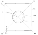
- the bonding member 2 has a rectangular outer shape with corners in the normal direction.
- the bonding member 2 is bonded to a portion of the other surface 11 b of the support substrate 11 of the piezoelectric element 1 that is different from the corner portion of the piezoelectric element 1 .
- the joining member 2 is arranged so that each corner of the joining member 2 protrudes from each opposing side of the piezoelectric element 1 in the normal direction.
- the joint member 2 is arranged so that the corners of the joint member 2 are positioned on a different portion from the imaginary line K4 connecting the opposite corners of the outer shape of the piezoelectric element 1 .
- the joining member 2 of the present embodiment is configured using a joining sheet having a predetermined outer shape.
- the electrode film 60 and the vibration region 22 of this embodiment are hexagonal in shape, and the vibration region 22 is octagon in the same manner as in the sixth embodiment.
- the electrode film 60 and the vibration region 22 are arranged so as to be point symmetric with respect to the central portion C. As shown in FIG. Note that the slit 40 is omitted in FIG. 39 .
- the vibration region 22 is supported on both sides. Therefore, the resonance frequency f of the piezoelectric element 1 can be increased, and the same effects as those of the first embodiment can be obtained.
- the joining member 2 is arranged at a portion different from the corner portion of the outer shape of the piezoelectric element 1 . Therefore, it is possible to suppress the propagation of thermal stress from the printed circuit board 101 to the corners of the piezoelectric element 1 where deformation is likely to increase. Therefore, the piezoelectric element 1 is less likely to deform due to the transmitted thermal stress, and the vibration region 22 is less likely to deform. As a result, it is possible to suppress a decrease in detection sensitivity and improve detection accuracy.
- the joint member 2 has a rectangular outer shape with corners.
- the joint member 2 is arranged so that the corners thereof are positioned on a different portion from the imaginary line K4 in the normal direction. Therefore, it is possible to suppress concentration of stress on the corner portion of the joining member 2 due to the deformation of the piezoelectric element 1, and it is possible to suppress the occurrence of problems such as peeling of the joining member 2.
- the joining member 2 may have an equilateral triangular shape in the normal direction as shown in FIG. 40A, or may have a regular octagonal shape in the normal direction as shown in FIG. 40B. Also, although not shown, the joining member 2 may have a regular hexagonal shape, a regular decagonal shape, or the like in the normal direction. The joining member 2 may be arranged so as to protrude from the piezoelectric element 1 in the normal direction, or may be arranged only inside the piezoelectric element 1 .
- the joint member 2 may be arranged as shown in FIGS. 41A to 41C with the through hole 101b formed in the printed circuit board 101 as a reference.
- 41A to 41C are plan views of the piezoelectric element 1 and the joining member 2 viewed from the side of the other surface 11b of the support substrate 11.
- 41A to 41C, the recess 10a formed in the support substrate 11 has a shape that matches the through hole 101b in the normal direction.
- the joint member 2 may have a ring shape surrounding the through hole 101b in the normal direction.
- the joint member 2 may have a +-shaped portion extending in one direction and a portion orthogonal to the one direction in the normal direction. good.
- the joining member 2 may be rhombic in the normal direction, as shown in FIG. 41C.
- the corner of the joining member 2 is positioned on the virtual line K4.
- the protrusion 101 c is shaped to match the outer shape of the joint member 2 and is formed of a part of the printed circuit board 101 .
- the projection 101c of the present embodiment is formed in a portion of the printed circuit board 101 that faces the piezoelectric element 1 and is different from the portion that faces the corner of the piezoelectric element 1 .
- the vibration region 22 is supported on both sides. Therefore, the resonance frequency f of the piezoelectric element 1 can be increased, and the same effects as those of the first embodiment can be obtained.
- the printed circuit board 101 is formed with a protrusion 101c. Therefore, when the liquid bonding member 2 is applied and arranged, the outer shape of the bonding member 2 to be bonded to the piezoelectric element 1 can be easily adjusted by applying the bonding member 2 onto the protrusion 101c. Therefore, a liquid material can be used as the bonding member 2, and the selectivity of the bonding member 2 can be improved. In particular, when adjusting the shape of the joining member 2 as in the tenth embodiment, the outer shape of the joining member 2 can be easily adjusted.
- the protrusion 101c may be configured by a member separate from the printed circuit board 101 .
- the piezoelectric film 50 is made of ScAlN.
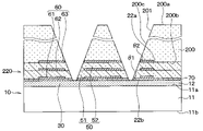
- the first slit 41 and the fourth slit 44 are formed to form a tapered portion 45 whose width narrows from the side of the one surface 22a toward the side of the other surface 22b.
- the first slit 41 and the fourth slit 44 are formed so that the side surface 22c becomes the tapered portion 45.
- the first slit 41 and the fourth slit 44 of the present embodiment are shaped so that the width continuously narrows from the side of the one surface 22a toward the side of the other surface 22b. That is, the first slit 41 is formed so that the side surface 22c of the vibration region 22 is substantially planar.
- first slit 41 and the fourth slit 44 are arranged so that the angle ⁇ 1 formed between the other surface 22b and the side surface 22c in the vibration region 22 (hereinafter simply referred to as the angle formed by the vibration region 22) is 39 to 81°. is formed in
- the formed angle ⁇ 1 can also be said to be the taper angle of the slit 40 .
- the second slit 42 and the third slit 43 have the same shape as the first slit 41 and the fourth slit 44 in a cross section different from that in FIG. FIG. 43 corresponds to a cross-sectional view along the IC--IC line in FIG.
- One surface 22a and the other surface 22b of the vibration region 22 are parallel to each other.
- the other surface 22b corresponds to a surface parallel to the one surface 22a.
- FIG. 44A to 44C correspond to cross-sectional views along the IC--IC line in FIG. 44A to 44C show cross-sectional views of the first slit 41 and the fourth slit 44, the same applies to the second and third slits 42 and 43.
- FIG. 44A to 44C correspond to cross-sectional views along the IC--IC line in FIG. 44A to 44C show cross-sectional views of the first slit 41 and the fourth slit 44, the same applies to the second and third slits 42 and 43.
- FIG. 44A to 44C correspond to cross-sectional views along the IC--IC line in FIG. 44A to 44C show cross-sectional views of the first slit 41 and the fourth slit 44, the same applies to the second and third slits 42 and 43.
- FIG. 44A to 44C correspond to cross-sectional views along the IC--IC line in FIG. 44A to 44C show cross-sectional views of the first slit 41 and the fourth
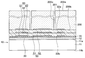
- an etching mask material 200 made of photoresist or the like is arranged so as to cover the upper electrode film 63 and the like, and the etching mask material 200 is formed with first to fourth slits 41 to 44.
- An opening 201 is formed in the portion where is formed.
- the second and third slits 42 and 43 are formed in a different cross section from that in FIG. 44A.
- the surface of the etching mask material 200 covering the upper electrode film 63 and the upper piezoelectric film 52 is referred to as the other surface 200b, and the surface of the etching mask material 200 opposite to the other surface 200b is referred to as the first surface 200a.
- a side surface of the opening 201 is defined as a side surface 200c.
- heat treatment is performed to adjust the shape of the openings 201 of the etching mask material 200 .
- the etching mask material 200 is arranged so as to cover the upper electrode film 63 and the upper piezoelectric film 52, and the portion on the other surface 200b side fixed thereto and the portion on the one surface 200a side are heated. They shrink differently. More specifically, when the heat treatment is performed, the portion of the etching mask material 200 on the other surface 200b side is difficult to thermally shrink, and the portion on the one surface 200a side is likely to thermally shrink.
- the angle ⁇ 2 formed between the other surface 200b and the side surface 200c of the etching mask material 200 (hereinafter also simply referred to as the angle ⁇ 2 formed by the etching mask material 200) is adjusted to the desired vibration region 22. Adjust according to the angle ⁇ 1.
- the piezoelectric film 50 and the etching mask material 200 are made of different materials, they usually have different etching rates when performing anisotropic dry etching, which will be described later. Therefore, based on the etching rate and the like, the angle ⁇ 2 formed by the etching mask material 200 is adjusted so that the angle ⁇ 1 formed by the vibration region 22 has a desired value. Since the angle ⁇ 2 formed by the etching mask material 200 is adjusted as described above, it may match the angle ⁇ 1 formed by the vibration region 22, but may not match the angle ⁇ 1 formed by the vibration region 22. There is also
- anisotropic dry etching is performed using the etching mask material 200 as a mask to form first to fourth slits 41 to 44 that penetrate the piezoelectric film 50 and reach the support 10 .
- the first to fourth slits 41 to 44 are formed so as to form the vibration area forming portion 220 having the side surface 22c that becomes the tapered portion 45. As shown in FIG. 44C , anisotropic dry etching is performed using the etching mask material 200 as a mask to form first to fourth slits 41 to 44 that penetrate the piezoelectric film 50 and reach the support 10 .
- the first to fourth slits 41 to 44 are formed so as to form the vibration area forming portion 220 having the side surface 22c that becomes the tapered portion 45.
- the angle ⁇ 2 formed by the etching mask material 200 is adjusted according to the angle ⁇ 1 formed by the vibration region 22, and the angle ⁇ 1 formed by the vibration region forming portion 220 is set to 39 to 81°. .
- the vibration region forming portion 220 is a portion that becomes the vibration region 22 by forming the concave portion 10a. Therefore, the angle ⁇ 1 formed by the vibration region forming portion 220 and the angle ⁇ 1 formed by the vibration region 22 are the same.
- the one surface, the other surface, and the side surface of the vibration region forming part 220 are given the same reference numerals as the one surface 22a, the other surface 22b, and the side surface 22c of the vibration region 22.
- the shapes of the lower electrode film 61, the intermediate electrode film 62, and the upper electrode film 63 are adjusted so as not to reach the first to fourth slits 41-44. Therefore, in this step, the piezoelectric film 50 and the base film 70 are anisotropically dry-etched.
- the same process as in FIG. 4C is performed to etch through the insulating film 12 from the other surface 11b of the support substrate 11 to reach the underlying film 70, thereby forming the recesses 10a.
- the vibration region forming portion 220 is suspended from the support 10 to form the vibration region 22, and the piezoelectric element 1 shown in FIG. 1 is manufactured.
- the piezoelectric film 50 such as ScAlN is subjected to anisotropic dry etching
- the following phenomenon is confirmed when the formed angle ⁇ 1 is 81° or more. That is, it has been confirmed that when the formed angle ⁇ 1 is 81° or more, the workability tends to decrease due to the effect of redeposition in which the etched atoms redeposit on the side surfaces 22c of the first to fourth slits 41 to 44. rice field.
- the piezoelectric film 50 such as ScAlN is subjected to anisotropic dry etching
- the following phenomenon is confirmed when the formed angle ⁇ 1 is 63° or more.
- the formed angle ⁇ 1 becomes 63° or more, the etched atoms redeposit near the openings of the first to fourth slits 41 to 44 on the side of the one surface 22a. was confirmed to be on the decline. Therefore, when forming the first to fourth slits 41 to 44, it is preferable that the angle ⁇ 1 formed by them is 63° or less. As a result, it is possible to prevent the workability from deteriorating due to fences or the like.
- ScAlN forming the piezoelectric film 50 is a hard-to-etch material. According to the studies of the present inventors, when forming the first to fourth slits 41 to 44 penetrating the piezoelectric film 50, in order to leave the etching mask material 200 on the piezoelectric film 50, , it was confirmed that the film thickness of the etching mask material 200 is preferably 1 to 5 times the film thickness of the piezoelectric film 50 . In other words, when forming the first to fourth slits 41 to 44 penetrating the piezoelectric film 50, in order to prevent the piezoelectric film 50 covered with the etching mask material 200 from being removed by the anisotropic dry etching, etching is required.
- the film thickness of the mask material 200 is preferably 1 to 5 times the film thickness of the piezoelectric film 50 . That is, as shown in FIG. 45, if the thickness of the piezoelectric film 50 is A1, the thickness A2 of the etching mask material 200 is preferably A1 to 5A1. Note that the base film 70 of the present embodiment is formed extremely thin with respect to the piezoelectric film 50 as described above. Therefore, the influence of the underlying film 70 is ignored. In other words, the film thickness A1 of the piezoelectric film 50 corresponds to the thickness h of the vibration region 22 described above.
- the first to fourth slits 41 to 44 are formed so as to have a narrow effective width.
- the effective width of the first to fourth slits 41-44 is the average width of the first to fourth slits 41-44.
- the slit width g continuously narrows from the one surface 22a to the other surface 22b as in the present embodiment, It is the average of the width and the width on the side of the other surface 22b.
- the angle ⁇ 1 formed by the vibration region constituting portion 220 is 39 to 81°.
- FIG. 47 summarizes the relationship between the ratio of the film thickness A2 of the etching mask material 200 to the film thickness A1 of the piezoelectric film 50 (hereinafter also referred to as film thickness ratio) and the formed angle.
- the resolution of the slit width g with respect to the film thickness A2 of the etching mask material 200 is limited to 1/2 to 1/3 of the film thickness A2 of the etching mask material 200.
- the lower limit of 39° for the formed angle ⁇ 1 corresponds to the case where the resolution is 1/2 times that of the etching mask material 200
- the upper limit corresponds to the case where the resolution is 1/3 times that of the etching mask material.
- the piezoelectric film 50 is made of an easily etched material such as AlN, and the side surface 22c of the vibration region 22 is substantially perpendicular to the other surface 22b.
- g be the effective width of the slit 40 in the piezoelectric element 1 of the comparative example. In this case, if the effective width of the piezoelectric element 1 of the present embodiment is greater than or equal to g, the slit width g of the first to fourth slits 41 to 44 may become too wide, resulting in lower sensitivity than the piezoelectric element 1 of the comparative example.
- the slits 40 are preferably formed so that the effective width is equal to or less than the effective width of the slits 40 in the piezoelectric element 1 of the comparative example. That is, it is preferable that tan ⁇ 1 is set to 1 or more. Therefore, ⁇ 1 is preferably 45° or more. As a result, it is possible to suppress a decrease in sensitivity. In this case, by setting ⁇ 1 to 63° or less, it is possible to suppress deterioration in workability of the slit 40 due to fences or the like.
- the vibration region 22 is supported on both sides. Therefore, the resonance frequency f of the piezoelectric element 1 can be increased, and the same effects as those of the first embodiment can be obtained.
- the angle ⁇ 1 formed by the vibration region 22 is set to 39 to 81°. Therefore, it is possible to prevent the workability of the slit 40 from deteriorating due to the film thickness A2 of the etching mask material 200, and the slit 40 can be preferably formed. Moreover, since the formed angle ⁇ 1 is 81° or less, it is possible to reduce the influence of redeposition, thereby suppressing deterioration of workability.
- This embodiment can also be applied to the case where the slits 40 are formed stepwise along the thickness direction of the vibrating region 22 as in the ninth embodiment.
- the angle between the other surface 22b and the line connecting the opening end of the slit 40 on the other surface 22b side and the opening end of the slit 40 on the one surface 22a side is The angle .theta.1 may be used.
- the slits 40 are formed each time the piezoelectric films 51 and 52 are formed. Therefore, in this configuration, the angle ⁇ 1 formed between the portion of each of the piezoelectric films 51 and 52 on the side of the other surface 20b and the side surface 20c may be set.
- the vibrating section 20 may be configured to have at least one layer of the piezoelectric film 50 and one layer of the electrode film 60 .
- the piezoelectric element 1 may have a polygonal shape such as a pentagonal shape or a hexagonal shape instead of a rectangular shape in plan view.
- the piezoelectric device S10 may have a configuration in which a through hole 102a is formed in the lid portion 102, as shown in FIG.
- the pressure-receiving surface space S1 is the space on the one surface 22a side of the vibration region 22 of the casing 100
- the back space S2 is the other surface 22b of the vibration region 22 of the casing 100. side space.
- the piezoelectric element 1 has been described in which the detection accuracy is improved by supporting the vibration region 22 on both sides.
- the detection accuracy can be improved by forming the slit 40 into a tapered shape.
- the shape of the piezoelectric film 50 and the electrode film 60 can improve the detection accuracy.
- the detection accuracy can be improved by changing the positional relationship between the slit 40 and the through hole 101b.
- the detection accuracy of the piezoelectric element 1 can be improved by reducing the low-frequency roll-off frequency.
- the positional relationship between the piezoelectric element 1 and the joining member 2 can improve the detection accuracy.
- the vibration region 22 may be cantilevered. That is, for example, when the outer shape of the vibration region 22 is a flat rectangular shape and the first to fourth slits 41 to 44 are formed in the vibration region 22, the first to fourth slits 41 to 44 vibrate. They may be formed so as to intersect at the central portion C of the region 22 . Since the manufacturing method in the twelfth embodiment relates to the shape of the slit 40, it can also be applied to the manufacturing method of the piezoelectric element 1 in which the vibration region 22 is cantilevered.
- the above embodiments can be combined as appropriate.
- the above-described second embodiment may be combined with the above-described third to twelfth embodiments, and the slit 40 may have a tapered shape in which the width becomes narrower toward the central portion C.
- the third embodiment may be combined with the fourth to twelfth embodiments to extract charges from the central region 225 of the vibrating region 22 as well.
- the fourth embodiment or the fifth embodiment may be combined with the sixth to twelfth embodiments, and the vibration region 22 may be supported by the connecting member 90 or the connecting member 91 on both sides.
- the sixth embodiment may be combined with the seventh to twelfth embodiments to define the shape and arrangement of the vibration region 22 and the electrode film 60 .
- the seventh embodiment may be combined with the eighth to twelfth embodiments, and the slit 40 may be formed in a portion different from the portion facing the through hole 101b.
- the slit length L may be defined by combining the eighth embodiment with the ninth to twelfth embodiments.
- the ninth embodiment may be combined with the tenth to twelfth embodiments, and the slit width g of the slit 40 may be changed along the thickness direction of the vibration region 22 .
- the tenth embodiment may be combined with the eleventh and twelfth embodiments to define the arrangement location of the joining member 2 .
- the eleventh embodiment may be combined with the twelfth embodiment to form the protrusion 101c on the printed circuit board 101.
- FIG. Further, combinations of the above embodiments may be further combined.
Landscapes
- Engineering & Computer Science (AREA)
- Manufacturing & Machinery (AREA)
- Chemical & Material Sciences (AREA)
- Ceramic Engineering (AREA)
- Physics & Mathematics (AREA)
- Acoustics & Sound (AREA)
- Signal Processing (AREA)
- Piezo-Electric Or Mechanical Vibrators, Or Delay Or Filter Circuits (AREA)
- Piezo-Electric Transducers For Audible Bands (AREA)
- Details Of Audible-Bandwidth Transducers (AREA)
Priority Applications (3)
| Application Number | Priority Date | Filing Date | Title |
|---|---|---|---|
| DE112022000948.9T DE112022000948T5 (de) | 2021-02-03 | 2022-02-01 | Piezoelektrisches element, piezoelektrische vorrichtung und verfahren zum herstellen eines piezoelektrischen elements |
| CN202280012733.XA CN116784020A (zh) | 2021-02-03 | 2022-02-01 | 压电元件、压电装置及压电元件的制造方法 |
| US18/356,487 US20230363280A1 (en) | 2021-02-03 | 2023-07-21 | Piezoelectric element, piezoelectric device, and method for manufacturing piezoelectric element |
Applications Claiming Priority (2)
| Application Number | Priority Date | Filing Date | Title |
|---|---|---|---|
| JP2021016148A JP7528804B2 (ja) | 2021-02-03 | 2021-02-03 | 圧電素子、圧電装置、および圧電素子の製造方法 |
| JP2021-016148 | 2021-02-03 |
Related Child Applications (1)
| Application Number | Title | Priority Date | Filing Date |
|---|---|---|---|
| US18/356,487 Continuation US20230363280A1 (en) | 2021-02-03 | 2023-07-21 | Piezoelectric element, piezoelectric device, and method for manufacturing piezoelectric element |
Publications (1)
| Publication Number | Publication Date |
|---|---|
| WO2022168826A1 true WO2022168826A1 (ja) | 2022-08-11 |
Family
ID=82741457
Family Applications (1)
| Application Number | Title | Priority Date | Filing Date |
|---|---|---|---|
| PCT/JP2022/003806 Ceased WO2022168826A1 (ja) | 2021-02-03 | 2022-02-01 | 圧電素子、圧電装置、および圧電素子の製造方法 |
Country Status (5)
| Country | Link |
|---|---|
| US (1) | US20230363280A1 (https=) |
| JP (2) | JP7528804B2 (https=) |
| CN (1) | CN116784020A (https=) |
| DE (1) | DE112022000948T5 (https=) |
| WO (1) | WO2022168826A1 (https=) |
Families Citing this family (3)
| Publication number | Priority date | Publication date | Assignee | Title |
|---|---|---|---|---|
| US12513467B2 (en) * | 2021-12-09 | 2025-12-30 | Skyworks Solutions, Inc. | Acoustic resistance improvement in piezoelectric microelectromechanical system microphone using compliant joint |
| US12549906B2 (en) * | 2022-03-31 | 2026-02-10 | Skyworks Solutions, Inc. | MEMS sensor with two compliances |
| CN119183056B (zh) * | 2024-11-25 | 2025-07-22 | 成都纤声科技有限公司 | 一种压电mems麦克风及其制备方法 |
Citations (5)
| Publication number | Priority date | Publication date | Assignee | Title |
|---|---|---|---|---|
| JP2009100178A (ja) * | 2007-10-16 | 2009-05-07 | Funai Electric Co Ltd | 携帯電話およびマイクロホンユニット |
| JP2011004129A (ja) * | 2009-06-18 | 2011-01-06 | Univ Of Tokyo | マイクロフォン |
| JP2018041788A (ja) * | 2016-09-06 | 2018-03-15 | 新日本無線株式会社 | 圧電素子 |
| WO2020121609A1 (ja) * | 2018-12-10 | 2020-06-18 | 株式会社村田製作所 | 圧電トランスデューサ |
| JP2020178109A (ja) * | 2019-04-23 | 2020-10-29 | 新日本無線株式会社 | 圧電素子 |
Family Cites Families (13)
| Publication number | Priority date | Publication date | Assignee | Title |
|---|---|---|---|---|
| JPS58100000U (ja) * | 1981-12-26 | 1983-07-07 | クラウン株式会社 | 音響変換装置 |
| JP3844784B2 (ja) * | 1997-09-08 | 2006-11-15 | 日本碍子株式会社 | 圧電/電歪デバイス |
| JP2003207729A (ja) | 2002-01-16 | 2003-07-25 | Ricoh Co Ltd | 形状可変鏡の製造方法及び光ディスク情報入出力装置 |
| WO2005050836A1 (ja) * | 2003-11-19 | 2005-06-02 | Murata Manufacturing Co., Ltd. | 端面反射型弾性表面波装置及びその製造方法 |
| JP4691395B2 (ja) * | 2005-05-30 | 2011-06-01 | 株式会社日立メディアエレクトロニクス | バルク弾性波共振器、バルク弾性波共振器を用いたフィルタ、それを用いた高周波モジュール、並びにバルク弾性波共振器を用いた発振器 |
| CN103460721B (zh) | 2011-03-31 | 2017-05-24 | 韦斯伯技术公司 | 具有间隙控制几何形状的声换能器以及声换能器制造方法 |
| JP6894719B2 (ja) * | 2017-02-21 | 2021-06-30 | 新日本無線株式会社 | 圧電素子 |
| JP2019114958A (ja) * | 2017-12-25 | 2019-07-11 | 第一精工株式会社 | 電気音響変換器 |
| JP2019161030A (ja) | 2018-03-14 | 2019-09-19 | 新日本無線株式会社 | 圧電素子 |
| JP7176678B2 (ja) | 2019-02-15 | 2022-11-22 | 日清紡マイクロデバイス株式会社 | 圧電素子 |
| DE112020002000T5 (de) * | 2019-05-16 | 2022-01-20 | Murata Manufacturing Co., Ltd. | Piezoelektrisches bauelement und ultraschallwandler |
| JP2021016148A (ja) | 2019-07-15 | 2021-02-12 | シャープ株式会社 | 走査アンテナおよび走査アンテナの製造方法 |
| WO2021095311A1 (ja) * | 2019-11-13 | 2021-05-20 | 株式会社村田製作所 | トランスデューサ |
-
2021
- 2021-02-03 JP JP2021016148A patent/JP7528804B2/ja active Active
-
2022
- 2022-02-01 DE DE112022000948.9T patent/DE112022000948T5/de active Pending
- 2022-02-01 WO PCT/JP2022/003806 patent/WO2022168826A1/ja not_active Ceased
- 2022-02-01 CN CN202280012733.XA patent/CN116784020A/zh active Pending
-
2023
- 2023-07-21 US US18/356,487 patent/US20230363280A1/en active Pending
-
2024
- 2024-07-23 JP JP2024117752A patent/JP7772148B2/ja active Active
Patent Citations (5)
| Publication number | Priority date | Publication date | Assignee | Title |
|---|---|---|---|---|
| JP2009100178A (ja) * | 2007-10-16 | 2009-05-07 | Funai Electric Co Ltd | 携帯電話およびマイクロホンユニット |
| JP2011004129A (ja) * | 2009-06-18 | 2011-01-06 | Univ Of Tokyo | マイクロフォン |
| JP2018041788A (ja) * | 2016-09-06 | 2018-03-15 | 新日本無線株式会社 | 圧電素子 |
| WO2020121609A1 (ja) * | 2018-12-10 | 2020-06-18 | 株式会社村田製作所 | 圧電トランスデューサ |
| JP2020178109A (ja) * | 2019-04-23 | 2020-10-29 | 新日本無線株式会社 | 圧電素子 |
Also Published As
| Publication number | Publication date |
|---|---|
| JP2024133375A (ja) | 2024-10-01 |
| CN116784020A (zh) | 2023-09-19 |
| JP7772148B2 (ja) | 2025-11-18 |
| DE112022000948T5 (de) | 2023-11-30 |
| US20230363280A1 (en) | 2023-11-09 |
| JP7528804B2 (ja) | 2024-08-06 |
| JP2022119126A (ja) | 2022-08-16 |
Similar Documents
| Publication | Publication Date | Title |
|---|---|---|
| US12487137B2 (en) | Piezoelectric element, piezoelectric device, and method of manufacturing piezoelectric element | |
| JP7772148B2 (ja) | 圧電素子、圧電装置 | |
| CN101379873B (zh) | 表面微机械加工的差动式传声器 | |
| US8733176B2 (en) | MEMS stress concentrating structure for MEMS sensors | |
| KR20080087172A (ko) | 컨덴서 마이크로폰 및 그 제조 방법과, 다이어프램 및 그 제조 방법 | |
| CN105282678A (zh) | 用于麦克风的系统和方法 | |
| EP3674258B1 (en) | Resonator and method of manufacturing the resonator, and strain sensor and sensor array including the resonator | |
| CN110113699B (zh) | 一种mems结构的制备方法 | |
| CN110149582B (zh) | 一种mems结构的制备方法 | |
| CN110113702B (zh) | 一种mems结构的制造方法 | |
| CN110149574A (zh) | 一种mems结构 | |
| JP2008252847A (ja) | 静電型トランスデューサ | |
| JP2022119126A5 (https=) | ||
| JP2007228345A (ja) | コンデンサマイクロホン | |
| JP4737535B2 (ja) | コンデンサマイクロホン | |
| JP4811035B2 (ja) | 音響センサ | |
| US20240284122A1 (en) | Mems microphone | |
| JP2008259062A (ja) | 静電型トランスデューサ | |
| TWI697999B (zh) | Mems裝置及製程 | |
| JP2026017787A (ja) | 圧電素子、マイクロフォン | |
| CN121865183A (zh) | 声音传感器 |
Legal Events
| Date | Code | Title | Description |
|---|---|---|---|
| 121 | Ep: the epo has been informed by wipo that ep was designated in this application |
Ref document number: 22749698 Country of ref document: EP Kind code of ref document: A1 |
|
| WWE | Wipo information: entry into national phase |
Ref document number: 202280012733.X Country of ref document: CN |
|
| WWE | Wipo information: entry into national phase |
Ref document number: 112022000948 Country of ref document: DE |
|
| 122 | Ep: pct application non-entry in european phase |
Ref document number: 22749698 Country of ref document: EP Kind code of ref document: A1 |