WO2022137288A1 - ワイヤ構造及びワイヤ構造形成方法 - Google Patents
ワイヤ構造及びワイヤ構造形成方法 Download PDFInfo
- Publication number
- WO2022137288A1 WO2022137288A1 PCT/JP2020/047715 JP2020047715W WO2022137288A1 WO 2022137288 A1 WO2022137288 A1 WO 2022137288A1 JP 2020047715 W JP2020047715 W JP 2020047715W WO 2022137288 A1 WO2022137288 A1 WO 2022137288A1
- Authority
- WO
- WIPO (PCT)
- Prior art keywords
- wire
- bump
- electronic component
- columnar bump
- columnar
- Prior art date
- Legal status (The legal status is an assumption and is not a legal conclusion. Google has not performed a legal analysis and makes no representation as to the accuracy of the status listed.)
- Ceased
Links
Images










Classifications
-
- H—ELECTRICITY
- H10—SEMICONDUCTOR DEVICES; ELECTRIC SOLID-STATE DEVICES NOT OTHERWISE PROVIDED FOR
- H10W—GENERIC PACKAGES, INTERCONNECTIONS, CONNECTORS OR OTHER CONSTRUCTIONAL DETAILS OF DEVICES COVERED BY CLASS H10
- H10W42/00—Arrangements for protection of devices
- H10W42/20—Arrangements for protection of devices protecting against electromagnetic or particle radiation, e.g. light, X-rays, gamma-rays or electrons
-
- H—ELECTRICITY
- H10—SEMICONDUCTOR DEVICES; ELECTRIC SOLID-STATE DEVICES NOT OTHERWISE PROVIDED FOR
- H10W—GENERIC PACKAGES, INTERCONNECTIONS, CONNECTORS OR OTHER CONSTRUCTIONAL DETAILS OF DEVICES COVERED BY CLASS H10
- H10W42/00—Arrangements for protection of devices
- H10W42/20—Arrangements for protection of devices protecting against electromagnetic or particle radiation, e.g. light, X-rays, gamma-rays or electrons
- H10W42/261—Arrangements for protection of devices protecting against electromagnetic or particle radiation, e.g. light, X-rays, gamma-rays or electrons characterised by their shapes or dispositions
- H10W42/265—Shielding wires, e.g. constant potential wires
-
- H—ELECTRICITY
- H10—SEMICONDUCTOR DEVICES; ELECTRIC SOLID-STATE DEVICES NOT OTHERWISE PROVIDED FOR
- H10W—GENERIC PACKAGES, INTERCONNECTIONS, CONNECTORS OR OTHER CONSTRUCTIONAL DETAILS OF DEVICES COVERED BY CLASS H10
- H10W42/00—Arrangements for protection of devices
- H10W42/20—Arrangements for protection of devices protecting against electromagnetic or particle radiation, e.g. light, X-rays, gamma-rays or electrons
- H10W42/281—Arrangements for protection of devices protecting against electromagnetic or particle radiation, e.g. light, X-rays, gamma-rays or electrons characterised by their materials
- H10W42/287—Arrangements for protection of devices protecting against electromagnetic or particle radiation, e.g. light, X-rays, gamma-rays or electrons characterised by their materials materials for magnetic shielding, e.g. ferromagnetic materials
-
- H—ELECTRICITY
- H10—SEMICONDUCTOR DEVICES; ELECTRIC SOLID-STATE DEVICES NOT OTHERWISE PROVIDED FOR
- H10W—GENERIC PACKAGES, INTERCONNECTIONS, CONNECTORS OR OTHER CONSTRUCTIONAL DETAILS OF DEVICES COVERED BY CLASS H10
- H10W72/00—Interconnections or connectors in packages
- H10W72/01—Manufacture or treatment
- H10W72/015—Manufacture or treatment of bond wires
-
- H—ELECTRICITY
- H10—SEMICONDUCTOR DEVICES; ELECTRIC SOLID-STATE DEVICES NOT OTHERWISE PROVIDED FOR
- H10W—GENERIC PACKAGES, INTERCONNECTIONS, CONNECTORS OR OTHER CONSTRUCTIONAL DETAILS OF DEVICES COVERED BY CLASS H10
- H10W72/00—Interconnections or connectors in packages
- H10W72/071—Connecting or disconnecting
-
- H—ELECTRICITY
- H10—SEMICONDUCTOR DEVICES; ELECTRIC SOLID-STATE DEVICES NOT OTHERWISE PROVIDED FOR
- H10W—GENERIC PACKAGES, INTERCONNECTIONS, CONNECTORS OR OTHER CONSTRUCTIONAL DETAILS OF DEVICES COVERED BY CLASS H10
- H10W72/00—Interconnections or connectors in packages
- H10W72/071—Connecting or disconnecting
- H10W72/072—Connecting or disconnecting of bump connectors
-
- H—ELECTRICITY
- H10—SEMICONDUCTOR DEVICES; ELECTRIC SOLID-STATE DEVICES NOT OTHERWISE PROVIDED FOR
- H10W—GENERIC PACKAGES, INTERCONNECTIONS, CONNECTORS OR OTHER CONSTRUCTIONAL DETAILS OF DEVICES COVERED BY CLASS H10
- H10W72/00—Interconnections or connectors in packages
- H10W72/071—Connecting or disconnecting
- H10W72/075—Connecting or disconnecting of bond wires
- H10W72/07551—Connecting or disconnecting of bond wires characterised by changes in properties of the bond wires during the connecting
- H10W72/07553—Connecting or disconnecting of bond wires characterised by changes in properties of the bond wires during the connecting changes in shapes
-
- H—ELECTRICITY
- H10—SEMICONDUCTOR DEVICES; ELECTRIC SOLID-STATE DEVICES NOT OTHERWISE PROVIDED FOR
- H10W—GENERIC PACKAGES, INTERCONNECTIONS, CONNECTORS OR OTHER CONSTRUCTIONAL DETAILS OF DEVICES COVERED BY CLASS H10
- H10W72/00—Interconnections or connectors in packages
- H10W72/50—Bond wires
-
- H—ELECTRICITY
- H10—SEMICONDUCTOR DEVICES; ELECTRIC SOLID-STATE DEVICES NOT OTHERWISE PROVIDED FOR
- H10W—GENERIC PACKAGES, INTERCONNECTIONS, CONNECTORS OR OTHER CONSTRUCTIONAL DETAILS OF DEVICES COVERED BY CLASS H10
- H10W72/00—Interconnections or connectors in packages
- H10W72/50—Bond wires
- H10W72/531—Shapes of wire connectors
-
- H—ELECTRICITY
- H10—SEMICONDUCTOR DEVICES; ELECTRIC SOLID-STATE DEVICES NOT OTHERWISE PROVIDED FOR
- H10W—GENERIC PACKAGES, INTERCONNECTIONS, CONNECTORS OR OTHER CONSTRUCTIONAL DETAILS OF DEVICES COVERED BY CLASS H10
- H10W74/00—Encapsulations, e.g. protective coatings
- H10W74/10—Encapsulations, e.g. protective coatings characterised by their shape or disposition
-
- H—ELECTRICITY
- H10—SEMICONDUCTOR DEVICES; ELECTRIC SOLID-STATE DEVICES NOT OTHERWISE PROVIDED FOR
- H10W—GENERIC PACKAGES, INTERCONNECTIONS, CONNECTORS OR OTHER CONSTRUCTIONAL DETAILS OF DEVICES COVERED BY CLASS H10
- H10W74/00—Encapsulations, e.g. protective coatings
- H10W74/40—Encapsulations, e.g. protective coatings characterised by their materials
-
- H—ELECTRICITY
- H10—SEMICONDUCTOR DEVICES; ELECTRIC SOLID-STATE DEVICES NOT OTHERWISE PROVIDED FOR
- H10W—GENERIC PACKAGES, INTERCONNECTIONS, CONNECTORS OR OTHER CONSTRUCTIONAL DETAILS OF DEVICES COVERED BY CLASS H10
- H10W90/00—Package configurations
-
- H—ELECTRICITY
- H10—SEMICONDUCTOR DEVICES; ELECTRIC SOLID-STATE DEVICES NOT OTHERWISE PROVIDED FOR
- H10W—GENERIC PACKAGES, INTERCONNECTIONS, CONNECTORS OR OTHER CONSTRUCTIONAL DETAILS OF DEVICES COVERED BY CLASS H10
- H10W99/00—Subject matter not provided for in other groups of this subclass
-
- H—ELECTRICITY
- H10—SEMICONDUCTOR DEVICES; ELECTRIC SOLID-STATE DEVICES NOT OTHERWISE PROVIDED FOR
- H10W—GENERIC PACKAGES, INTERCONNECTIONS, CONNECTORS OR OTHER CONSTRUCTIONAL DETAILS OF DEVICES COVERED BY CLASS H10
- H10W72/00—Interconnections or connectors in packages
- H10W72/071—Connecting or disconnecting
- H10W72/0711—Apparatus therefor
-
- H—ELECTRICITY
- H10—SEMICONDUCTOR DEVICES; ELECTRIC SOLID-STATE DEVICES NOT OTHERWISE PROVIDED FOR
- H10W—GENERIC PACKAGES, INTERCONNECTIONS, CONNECTORS OR OTHER CONSTRUCTIONAL DETAILS OF DEVICES COVERED BY CLASS H10
- H10W72/00—Interconnections or connectors in packages
- H10W72/071—Connecting or disconnecting
- H10W72/075—Connecting or disconnecting of bond wires
-
- H—ELECTRICITY
- H10—SEMICONDUCTOR DEVICES; ELECTRIC SOLID-STATE DEVICES NOT OTHERWISE PROVIDED FOR
- H10W—GENERIC PACKAGES, INTERCONNECTIONS, CONNECTORS OR OTHER CONSTRUCTIONAL DETAILS OF DEVICES COVERED BY CLASS H10
- H10W72/00—Interconnections or connectors in packages
- H10W72/20—Bump connectors, e.g. solder bumps or copper pillars; Dummy bumps; Thermal bumps
Definitions
- the present invention relates to a configuration of a wire structure including a columnar bump and a looping wire looped so as to straddle over an electronic component, and a method for forming the wire structure.
- the end on the starting point side of the bonding is such that the wire is vertically raised with the tip of the wire bonded on the substrate, and the wire is raised at a large angle. Since it can be bent laterally, the wire does not come into contact with the electronic component even if the starting point of bonding is placed close to the electronic component. However, since it is difficult to bend the looping wire toward the substrate on the end point side of the bonding, it is necessary to set the end point of the bonding at a position away from the electronic component (see paragraph 0013 of Patent Document 1). Therefore, when the looping wire straddling the electronic component is formed by the method of Patent Document 1, a wide space for forming the looping wire is required, and there is a problem that the electronic device becomes large.
- an object of the present invention is to provide a wire structure capable of magnetically shielding electronic components in a small space.
- the wire structure of the present invention includes a columnar bump provided adjacent to an electronic component mounted on a substrate and a looping wire bonded onto the substrate so as to straddle the electronic component.
- the looping wire is engaged with a rising portion whose tip is bonded to the substrate on the opposite side of the electronic component of the columnar bump and rises from the substrate, a loop portion extending so as to straddle the electronic component, and the upper end of the columnar bump. It is characterized by including a bent portion that bends so as to connect the loop portion and the rising portion.
- the bent portion engages with the upper end of the columnar bump and bends, the bending angle of the bent portion can be increased, and the rising portion can be raised from the substrate at an angle close to vertical.
- the tip of the rising portion is bonded to a position adjacent to the electronic component, it is possible to prevent the upper portion of the rising portion and the bent portion from coming into contact with the electronic component, and the wire structure enables magnetic shielding of the electronic component in a small space. Can be provided.
- the columnar bump has a groove extending in the extending direction of the loop portion at the upper end, and the bent portion may engage with the groove.
- the bent portion can be stably engaged with the upper end of the columnar bump, and the bent portion can be stably formed with a large bending angle.
- the bent portion may have a bending angle of 60 ° to 90 °.
- the rising portion can be raised from the substrate at an angle close to vertical, and a compact wire structure can be obtained.
- the height of the columnar bumps may be 50% or more of the height from the substrate to the loop portion.
- the wire structure forming method of the present invention is a wire structure forming method for forming a wire structure including columnar bumps and looping wires by a bonding tool, in which a plurality of wires are diffracted and overlapped at bump points on a substrate by the bonding tool.
- the bonding tool is raised to feed out the wire from the tip of the bonding tool, and the bonding tool is moved laterally to form a kink wire having at least one kink.
- the bonding tool is looped toward the upper end of the columnar bump to form a loop portion straddling the electronic component between the first bond point and the upper end of the columnar bump.
- the side surface of the kink wire is engaged with the upper end of the columnar bump and the kink wire is bent toward the substrate to form the bending portion.
- the kink wire is bonded to the second bond point located on the substrate adjacent to the side opposite to the first bond point from the bump point with a bonding tool, and the rising portion that rises from the second bond point and connects to the bent portion. It is characterized by including a rising portion forming step of forming the above.
- the bonding tool is looped to the upper end of the columnar bump to engage the side surface of the kink wire with the upper end of the columnar bump to bend the kink wire, so that a bent portion having a large bending angle is formed.
- the rising part can be raised from the substrate at an angle close to vertical.
- the bonding tool is a capillary provided with a through hole through which the wire is inserted and an annular face portion provided around the through hole, and the columnar bump forming step folds the side surface of the wire.
- the center position of the capillary is shifted in the direction intersecting with the extending direction of the loop portion, the side surface of the wire is pressed by the face portion, and the loop portion extends to the upper end of the columnar bump. Grooves extending in the direction may be formed.
- the side surface of the kink wire may be engaged with the groove by a bonding tool to bend the kink wire toward the substrate.
- the bent portion can be stably engaged with the upper end of the columnar bump, and a bent portion having a large bending angle can be stably formed.
- the wire may be ball-bonded to the first bond point in the first bonding step, and stitch bonding may be performed to the second bond point in the rising portion forming step.
- the columnar bump forming step further forms other columnar bumps at other bump points arranged between the first bond point and the electronic component
- the loop portion forming step is a kink wire.
- the bonding tool is looped towards the top edge of the columnar bump to form a loop that straddles the electronic component between the first bond point and the top edge of the columnar bump.
- the kink wire may be bent upward of the electronic component by engaging with the upper end of the columnar bump to form another bent portion.
- the space for forming the wire structure on the first bond point side can be reduced, and the wire structure capable of magnetically shielding the electronic component can be formed in a smaller space.
- the electronic device of the present invention has a substrate, an electronic component mounted on the substrate, a columnar bump provided adjacent to the electronic component, and a looping bonded onto the substrate so as to straddle the electronic component.
- An electronic device equipped with a wire The looping wire engages with the rising portion where the tip is bonded to the substrate on the opposite side of the electronic component of the columnar bump and rises from the substrate, the loop portion extending so as to straddle the electronic component, and the upper end of the columnar bump. It is characterized by including a bent portion that bends so as to connect the portion and the rising portion.
- the columnar bump has a groove extending in the extending direction of the loop portion at the upper end, and the bent portion may engage with the groove.
- the present invention can provide a wire structure capable of magnetically shielding electronic components in a small space.
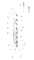
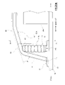
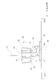
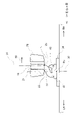
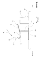
- FIG. 6 is a cross-sectional view of an electronic device provided with a wire structure according to an embodiment, and is a cross-sectional view taken along the line AA shown in FIG. It is an elevation view which shows the detail of the part B shown in FIG.
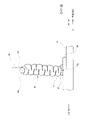
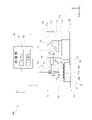
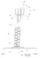
- FIG. 3 is an elevation view of the columnar bumps of the wire structure of the embodiment as viewed from DD shown in FIG. It is an elevation view which shows the detail of part C shown in FIG. It is an elevation view which shows the structure of the wire bonding apparatus used for manufacturing the electronic apparatus which comprises the wire structure of embodiment. It is sectional drawing of the capillary attached to the wire bonding apparatus shown in FIG.
- FIG. 9 is a diagram showing a state in which the capillary is laterally moved to the left side from the state shown in FIG. 9E and the face portion on the right side is positioned directly above the ball neck. It is a figure which shows the state which formed the crushed part by pressing the side surface of a wire on the ball neck with the face part on the right side of a capillary. It is a figure which shows the state which raised the capillary from the state of FIG. 9G.
- FIG. 9 is a diagram showing a state in which the capillary is laterally moved to the right side from the state shown in FIG.
- FIG. 9H shows the face portion on the left side is positioned directly above the crushed portion.
- FIG. 9J shows the state which formed the folded part by pressing the side surface of a wire on the crushed part by the face part on the left side of a capillary.
- the capillary is raised to form a columnar shape by alternately folding the side surfaces of the wire from the left and right to form a columnar shape as shown in FIGS. 9H to 9J.
- It is an elevation view which shows the state which formed the columnar bump which has the groove extending in the front-rear direction by pressing the side surface of.
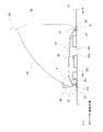
- FIG. 11A is a diagram showing a state in which the tip of the capillary is looped toward a columnar bump from the state of FIG. 11A to form a first rising portion and a loop portion. It is an elevation view which shows the detailed view of the E part of FIG. 11B.
- 11B is an elevational view showing a state in which the tip of the capillary is moved downward in an arc shape toward the second bond point from the state shown in FIGS. 11B and 11C to form a bent portion.
- 11 is an elevational view showing a state in which the tip of the capillary is lowered from the state of FIG. 11D and stitch-bonded onto the second pad to form a bent portion, a second rising portion, and a stitch-bonded portion. It is an elevation view which shows the detail of the F part of FIG. 11E. It is an elevation view which shows the 1st rise part of the wire structure of another embodiment.
- the electronic device 30 of the embodiment includes a substrate 31, first to fourth electronic components 32a to 32d mounted on the substrate 31, columnar bumps 45, and looping wires 50. There is.
- the columnar bump 45 and the looping wire 50 form the wire structure 50A of the embodiment.
- the first electronic component 32a is attached to the center of the board 31.
- the first electronic component 32a may be, for example, a semiconductor chip or an IC.
- second and third electronic components 32b and 32c are attached to both sides of the first electronic component 32a.
- the second and third electronic components 32b and 32c may be, for example, a capacitor or an inductor.
- the fourth electronic component 32d is attached.
- the fourth electronic component 32d may be, for example, a resistor or the like.
- a first metal pad 33, a second pad 34, a left side pad 35, and a right side pad 36 are provided on the surface of the substrate 31 around the first to fourth electronic components 32a to 32d.
- the first bond point P1 of the looping wire 50 is arranged on the first pad 33.
- a second bond point P2 of the looping wire 50 and a bump point Pb forming the columnar bump 45 are arranged on the second pad 34.
- the second bond point P2 is arranged on the side opposite to the first bond point P1 or the second electronic component 32b from the bump point Pb.
- the bump points Pb and the first bond points P1 are arranged on the substrate 31 so as to sandwich the first to fourth electronic components 32a to 32d.
- the direction from the first bond point P1 to the second bond point P2 is forward
- the direction from the first bond point P1 to the opposite side to the second bond point P2 is backward
- the left side toward the front will be described with the right side as the right side.
- the extending direction of the first bond point P1 and the second bond point P2 will be described as the front-rear direction, and the direction perpendicular to this will be described as the left-right direction.
- the reference numeral “F” in each figure indicates the front
- the reference numeral “R” indicates the rear
- the reference numeral “LH” indicates the left side
- the reference numeral “RH” indicates the right side.
- columnar bumps 45 are formed at the bump points Pb arranged on the side (rear side) of the third electronic component 32b on the second pad 34.
- the columnar bump 45 is a columnar bump formed so as to be adjacent to the third electronic component 32b.
- the columnar bump 45 includes a crimping ball 41 and a plurality of folded portions 44.
- the side surface of the wire 16 is alternately folded from the left and right a plurality of times on the crimping ball 41 formed on the second pad 34, and the folded portions 44 are formed in a plurality of stages. It is formed into columns.
- a groove 48 extending in the front-rear direction is formed at the upper end of the columnar bump 45. Since the looping wire 50 is bonded to the first bond point P1 and the second bond point P2 of the substrate 31 so as to extend in the front-rear direction, the groove 48 extends in the extending direction of the looping wire 50.
- the height of the columnar bump 45 is substantially the same as the height of the adjacent second electronic component 32b, but it can be made lower than this, for example, the adjacent second electronic component.
- the height may be about 50% of the height of the component 32b. Further, the height may be higher than the height of the adjacent second electronic component 32b.
- the looping wire 50 straddles the first to third electronic components 32a to 32c so as to straddle the first bond point P1 of the first pad 33 and the second bond point P2 of the second pad 34. It is bonded to.
- the looping wire 50 extends in the front-rear direction and includes a crimping ball 51, a first rising portion 53, a second rising portion 54, a loop portion 55, a bending portion 56, and a stitch bond portion 57.
- the crimping ball 51 is a disk-shaped portion in which the free air ball 40 is bonded onto the first pad 33.
- the first rising portion 53 is a portion that extends upward from above the crimping ball 51, then bends forward and extends to the vicinity of the upper side of the third electronic component 32c.
- the loop portion 55 is a portion connected to the first rising portion 53 and extending in the front-rear direction so as to straddle the first to fourth electronic components 32a to 32d.
- the second rising portion 54 is a portion that rises diagonally upward from the stitch bond portion 57 stitch-bonded on the second pad 34.
- the bent portion 56 is a portion that engages with a groove 48 extending in the front-rear direction formed at the upper end of the columnar bump 45 and bends so as to connect the loop portion 55 and the second rising portion 54.
- the bending angle ⁇ of the bending portion 56 may be, for example, between 60 ° and 90 °.
- the bent portion 56 of the looping wire 50 engages with the groove 48 provided at the upper end of the columnar bump 45 and bends, so that the bending angle ⁇ of the bent portion 56 is increased. Can be done.
- the second rising portion 54 can be raised from the second pad 34 of the substrate 31 at an angle close to vertical. Therefore, even if the tip of the second rising portion 54 is stitch-bonded to a position adjacent to the second electronic component 32a, the upper portion of the second rising portion 54 and the bent portion 56 are in contact with the adjacent second electronic component 32b. It can be suppressed, and the magnetic shield of the first to fourth electronic components 32a to 32d can be performed in a small space.
- the looping wire 50 is bonded onto the first pad 33 and the second pad 34, and the looping wire 50 extends in the front-rear direction to form the first to fourth electronic components 32a to 32d. I explained that it straddles the top, but it is not limited to this.
- the looping wire 50 may be bonded on the left side pad 35 and the right side pad 36 so as to extend in the left-right direction. Further, the looping wire 50 may be bonded so as to extend in an oblique direction between the first pad 33 and the left side pad 35 or the right side pad 36.
- the wire bonding device 100 is a manufacturing device for the electronic device 30.
- the wire bonding apparatus 100 includes a base 10, an XY table 11, a bonding head 12, a Z-direction motor 13, a bonding arm 14, an ultrasonic horn 15, and a capillary that is a wire bonding tool. 20, a wire clamper 17, a discharge electrode 18, a bonding stage 19, and a control unit 60 are provided.
- the extending direction of the bonding arm 14 or the ultrasonic horn 15 will be described as the X direction
- the direction perpendicular to the X direction on the horizontal plane will be described as the Y direction
- the vertical direction will be described as the Z direction.
- the XY table 11 is mounted on the base 10 and is mounted on the upper side to move in the XY direction.
- the bonding head 12 is mounted on the XY table 11 and moves in the XY direction by the XY table 11.
- a Z-direction motor 13 and a bonding arm 14 driven by the Z-direction motor 13 are housed in the bonding head 12.
- the Z-direction motor 13 includes a stator 13b.
- the bonding arm 14 is a rotor whose root portion 14a faces the stator 13b of the Z-direction motor 13 and is rotatably attached around the shaft 13a of the Z-direction motor 13.
- An ultrasonic horn 15 is attached to the tip of the bonding arm 14 in the X direction, and a capillary 20 is attached to the tip of the ultrasonic horn 15.
- the ultrasonic horn 15 ultrasonically vibrates a capillary 20 attached to the tip by vibration of an ultrasonic vibrator (not shown).
- the capillary 20 is provided with a through hole 21 that penetrates in the vertical direction inside, and a wire 16 is inserted through the through hole 21.
- the wire 16 is supplied from a wire supply such as a wire spool (not shown).
- a wire clamper 17 is provided on the upper side of the tip of the ultrasonic horn 15. The wire clamper 17 opens and closes to grip and open the wire 16.
- a discharge electrode 18 is provided on the upper side of the bonding stage 19.
- the discharge electrode 18 may be attached to a frame (not shown) provided on the base 10.
- the discharge electrode 18 is inserted into the capillary 20 to discharge electricity from the wire 16 extending from the tip 25 of the capillary 20, and the wire 16 is melted to form a free air ball 40.
- the bonding stage 19 sucks and fixes the substrate 31 on which the first to fourth electronic components 32a to 32d are attached on the upper surface, and heats the substrate 31 with a heater (not shown).
- the root portion 14a of the bonding arm 14 constituting the rotor When the root portion 14a of the bonding arm 14 constituting the rotor is rotated as shown by the arrow 71 in FIG. 6 by the electromagnetic force of the stator 13b of the Z-direction motor 13 of the bonding head 12, it is attached to the tip of the ultrasonic horn 15.
- the obtained capillary 20 moves in the Z direction as shown by the arrow 72.
- the bonding stage 19 is moved in the XY direction by the XY table 11. Therefore, the capillary 20 is moved in the XYZ direction by the XY table 11 and the Z direction motor 13.
- the wire clamper 17 moves in the XYZ direction together with the capillary 20. Therefore, the XY table 11 and the Z-direction motor 13 form a moving mechanism 11a that moves the capillary 20 and the wire clamper 17 in the XYZ direction.
- the XY table 11, the Z-direction motor 13, the wire clamper 17, the discharge electrode 18, and the bonding stage 19 are connected to the control unit 60, and operate based on the command of the control unit 60.
- the control unit 60 adjusts the position of the capillary 20 in the XYZ direction by the moving mechanism 11a composed of the XY table 11 and the Z-direction motor 13, opens and closes the wire clamper 17, drives the discharge electrode 18, and bonds the bonding stage 19. The heating is controlled.
- the control unit 60 is a computer including a CPU 61, which is a processor that processes information internally, and a memory 62 that stores an operation program, operation data, and the like.
- FIG. 7 is a diagram showing an example of the tip end portion of the capillary 20.
- the capillary 20 is formed with a through hole 21 penetrating in the direction of the center line 24 passing through the center position.
- the wire 16 is inserted into the through hole 21. Therefore, the inner diameter d1 of the through hole 21 is larger than the outer diameter d2 of the wire 16 (d1> d2).
- the lower end of the through hole 21 extends in a conical shape. This conical tapered portion is called a chamfer portion 22.
- the maximum diameter (that is, the diameter at the lowermost end) of this conical space is called the chamfer diameter d3.
- the lower end surface of the capillary 20 is an annular face portion 23 that presses the free air ball 40 shown in FIG.
- the face portion 23 may be a flat horizontal surface or an inclined surface that moves upward as it approaches the outside.
- the width of the face portion 23, that is, the distance between the chamfer portion 22 and the outer circumference of the lower end of the capillary 20 is referred to as "face width W".
- the point above the center line 24 at the lower end of the capillary 20 is referred to as the tip 25 of the capillary 20.
- the CPU 61 which is the processor of the control unit 60, first opens the wire clamper 17, drives and controls the XY table 11 and the Z-direction motor 13, and moves the tip 25 of the capillary 20 to the vicinity of the discharge electrode 18. Then, the CPU 61 generates a discharge between the discharge electrode 18 and the wire tail extending from the tip 25 of the capillary 20, and as shown in FIG. 9A, the wire 16 extending from the tip 25 of the capillary 20 is free air. It is molded into a ball 40.
- the CPU 61 drives and controls the XY table 11 and the Z-direction motor 13, and sets the XY coordinates of the center line 24 of the capillary 20 to the bump point Pb on the second pad 34. Align with the XY coordinates of the center line 38. Then, the CPU 61 lowers the tip 25 of the capillary 20 toward the bump point Pb to the point a as shown by the arrow 81 shown in FIGS. 8 and 9B, and is free at the face portion 23 of the capillary 20 as shown in FIG. 9B. Ball bonding is performed by pressing the air ball 40 onto the second pad 34.
- the capillary 20 presses the free air ball 40 onto the second pad 34, the face portion 23 and the chamfer portion 22 form the free air ball 40 as a crimping ball 41, as described above with reference to FIG. And the ball neck 42.
- the CPU 61 drives and controls the XY table 11 and the Z-direction motor 13 to point to the tip 25 of the capillary 20 as shown by the arrow 82 shown in FIGS. 8 and 9C. Raise to b.
- the CPU 61 laterally moves the tip 25 of the capillary 20 toward the right side to the point c as shown by the arrow 83 shown in FIGS. 8 and 9D.
- the CPU 61 raises the tip 25 of the capillary 20 to the point d as shown by the arrow 84 shown in FIGS. 8 and 9E.
- the CPU 61 moves the capillary 20 to a position where the center of the face portion 23 on the right side of the capillary 20 in the face width direction becomes the XY coordinates of the center line 38 of the bump point Pb, as shown by the arrow 85 in FIGS. 8 and 9F. Move laterally to the left.
- the CPU 61 drives and controls the XY table 11 and the Z-direction motor 13 to lower the tip 25 of the capillary 20 to the point f as shown by the arrows 86 shown in FIGS. 8 and 9G, on the ball neck 42.
- the side surface of the wire 16 folded back to the right side and the left side is pressed onto the ball neck 42 and crushed to form the crushed portion 43.
- the CPU 61 raises the tip 25 of the capillary 20 to the point g as shown by the arrow 87 shown in FIGS. 8 and 9H, and then the face portion on the left side of the capillary 20 as shown by the arrow 88 shown in FIGS. 8 and 9I.
- the capillary 20 is laterally moved to the right side to a position where the center of 23 in the face width direction is the XY coordinate of the center line 38 of the bump point Pb.
- the CPU 61 drives and controls the XY table 11 and the Z-direction motor 13 to lower the tip 25 of the capillary 20 to the point i as shown by the arrows 89 shown in FIGS. 8 and 9J, and the crushing portion 43.
- the side surface of the wire 16 is pressed upward to form the folded portion 44.
- the CPU 61 drives and controls the XY table 11 and the Z-direction motor 13 to raise the capillary 20, and alternately folds the side surfaces of the wire 16 from the left and right as shown in FIGS. 9H to 9J.
- the portion 44 is formed in a plurality of stages to form a columnar bump 45.
- the CPU 61 moves the capillary 20 to a position where the center of the face portion 23 on the left side of the capillary 20 in the face width direction becomes the XY coordinates of the center line 38 of the bump point Pb, and the CPU 61 moves the capillary 20 to a position as shown by the arrow 90 shown in FIG. 9K.
- the tip 25 of the capillary 20 is lowered to the point j, and the side surface of the wire 16 is pressed onto the folded portion 44 to form the uppermost folded portion 44.
- a groove 48 extending in the front-rear direction is formed on the upper surface of the uppermost folded portion 44 by the face portion 23.
- the folded portion 44 at the uppermost stage and the wire 16 contained in the through hole 21 of the capillary 20 are connected by a thin connecting portion 46.
- the CPU 61 drives and controls the XY table 11 and the Z-direction motor 13 to raise the capillary 20 and extend the wire tail 47 from the tip 25 of the capillary 20 as shown by the arrow 91 shown in FIG. 9L.
- the CPU 61 closes the wire clamper 17 and raises the wire clamper 17 and the capillary 20 further to cut the lower end of the wire tail 47 connected to the wire supply and the connecting portion 46.
- a columnar bump 45 is formed on the second pad 34.
- the side surfaces of the wire 16 are alternately folded from the left and right by repeatedly executing the raising of the capillary 20, the movement in the left-right direction, and the pressing by the lowering to form the folded portion 44 in a plurality of stages.
- the columnar bump 45 can be formed.
- the position of the center line 24 of the capillary 20 is the XY coordinates of the center line 38 of the bump point Pb at the center of the face portion 23 on the left side of the capillary 20 in the face width direction.
- the side surface of the wire 16 is pressed so as to be shifted to the right side of the position of the center line 38 of the columnar bump 45.
- the position of the center line 24 of the capillary 20 is shifted from the position of the center line 38 of the columnar bump 45 to the left-right direction intersecting the front-rear direction, which is the direction in which the loop portion 55 extends, and the side surface of the wire 16 is pressed by the face portion 23. do.
- a groove 48 extending in the front-rear direction can be formed at the upper end of the columnar bump 45.
- the CPU 61 of the control unit 60 drives and controls the XY table 11 and the Z-direction motor 13 to form a free air ball 40 at the tip of the wire 16 as described above with reference to FIGS. 9A and 9B.
- the capillary 20 is lowered onto the first pad 33 to form a crimping ball 51 on the first pad 33 (first bonding step).
- the CPU 61 drives and controls the XY table 11 and the Z-direction motor 13 so as to pass from the first bond point P1 to each point S1 to S12 as shown by arrows 92a to 92k in FIG.
- the ascent of 20 and the movement in the front-rear direction are repeated to form a kink wire 52 having a first kink 52a, a second kink 52b, and a third kink 52c as shown in FIG. 11A (kink wire forming step).
- the CPU 61 loops the tip 25 of the capillary 20 toward the upper end of the columnar bump 45 as shown by the arrow 93 in FIG. 11B, so that the first bond point P1 and the upper end of the columnar bump 45 are first.
- the loop portion 55 of the looping wire 50 straddling the third electronic components 32a to 32c is formed (loop portion forming step).
- the portion of the kink wire 52 including the first kink 52a and the second kink 52b rises from above the crimping ball 51 on the first pad 33 as shown in FIGS. 5 and 11B, and of the third electronic component 32c. It is formed on the first rising portion 53 of the looping wire 50 facing upward. Further, as shown in FIG.
- the CPU 61 drives and controls the XY table 11 and the Z-direction motor 13, and as shown by the arrow 94 in FIG. 11D, the tip 25 of the capillary 20 is arcuate downward toward the second bond point P2. Move it. As a result, the tip 25 of the capillary 20 engages the side surface of the kink wire 52 with the groove 48 at the upper end of the columnar bump 45, and the front side of the portion engaged with the groove 48 of the kink wire 52 is the second of the substrate 31. It is bent toward the pad 34 to form a bent portion 56 of the looping wire 50 (bending portion forming step).
- the CPU 61 drives and controls the XY table 11 and the Z-direction motor 13 to move the tip 25 of the capillary 20 further downward toward the second bond point P2, as shown by the arrows 94 in FIGS. 11E and 11F.
- the tip 25 of the capillary 20 is lowered toward the second bond point P2, and the tip of the kink wire 52 is placed on the second pad 34. Stitch bond on the second bond point P2 of.
- the stitch bond portion 57 of the looping wire 50 and the second rising portion 54 of the looping wire 50 that rises from the stitch bond portion 57 and connects to the bent portion 56 are formed on the second pad 34 (the rising portion is formed). Process).
- the CPU 61 closes the wire clamper 17 and raises the wire clamper 17 and the capillary 20 to cut the wire 16 connected to the wire supply and the stitch bond portion 57. This completes the formation of the looping wire 50.
- the kink wire 52 is looped to the upper end of the columnar bump 45, and the side surface of the kink wire 52 is engaged with the groove 48 at the upper end of the columnar bump 45 to bend the kink wire 52.
- the bent portion 56 having a large bending angle ⁇ can be formed, and the second rising portion 54 can be raised from the second pad 34 of the substrate 31 at an angle close to vertical.
- the wire structure 50B of another embodiment will be described with reference to FIG. As shown in FIG. 12, the wire structure 50B is composed of a columnar bump 45a and a looping wire 50a.
- the columnar bump 45a is formed on the bump point Pb1 arranged on the side of the second bond point P2 with respect to the first bond point P1 on the first pad 33. Similar to the columnar bump 45 described above with reference to FIGS. 1 to 9L, the columnar bump 45a includes a crimping ball 41 and a plurality of folded portions 44, and a groove 48 extending in the front-rear direction is provided at the upper end thereof. Has been done.
- the looping wire 50a is bonded onto the substrate 31 so as to straddle the first to fourth electronic components 32a to 32d.
- the pad 33 and the second pad 34 are connected.
- the looping wire 50a is different from the looping wire 50a in that the side of the first pad 33 is composed of a crimping ball 51a, a first rising portion 53a, a bent portion 56a, and a loop portion 55a.
- Other configurations are the same as the looping wire 50a described above.
- the first rising portion 53a is a portion that rises diagonally upward from the crimping ball 51a on the first pad 33.
- the bent portion 56a is a portion connected to the first rising portion 53a and bent from the rising direction toward the upper side of the third electronic component 32c at the upper end of the columnar bump 45.
- the bending angle ⁇ 2 of the bending portion 56a may be, for example, between 60 ° and 90 °.
- the loop portion 55a is a portion connected to the bent portion 56a and extending from the vertical direction at the upper end of the columnar bump 45a across the first to third electronic components 32a to 32c to the second bond point P2.
- the columnar bumps 45 are first placed on the bump points Pb and Pb1 of the first pad 33 and the second pad 34 in the same manner as previously referred to FIGS. 9A to 9L. , 45a (columnar bump generation step).
- first bonding step ball bonding is performed at the first bond point P1 to form a crimping ball 51 (first bonding step).
- the capillary 20 is raised to feed out the wire 16 from the tip 25 of the capillary 20, and the capillary 20 is moved laterally to form the kink wire 52 (kink wire forming step).
- the bending angle of the first kink 52a shown in FIG. 11A is smaller than that in the case of forming the wire structure 50A, or the first kink 52a is not formed and only the second and third kinks 52b and 52c are formed. To do so.
- the capillary 20 is looped toward the upper end of the columnar bump 45 formed on the second pad 34.
- the side surface of the kink wire 52 engages with the groove 48 at the upper end of the columnar bump 45a formed on the first pad 33, and the kink wire 52 bends upward by the bending angle ⁇ 2 of the third electronic component 32c.
- the bent portion 56a is formed.
- a loop portion 55a connected to the bent portion 56a and extending toward the second bond point P2 is formed.
- the bent portion 56a is a portion that engages with the upper end of the columnar bump 45a and bends so as to connect the loop portion 55a and the first rising portion 53a.
- the bending portion generation step and the rising portion formation are performed as described with reference to FIGS. 11B to 11F.
- the steps are performed to form the looping wire 50a.
Landscapes
- Wire Bonding (AREA)
- Physics & Mathematics (AREA)
- Health & Medical Sciences (AREA)
- Electromagnetism (AREA)
- Toxicology (AREA)
Abstract
Description
ルーピングワイヤは、先端が柱状バンプの電子部品と反対側で基板にボンディングされて基板から立ち上がる立ち上がり部と、電子部品の上を跨ぐように延びるループ部と、柱状バンプの上端に係合してループ部と立ち上がり部とを接続するように屈曲する屈曲部と、を備えることを特徴とする。
Claims (11)
- 基板の上に取付けられた電子部品に隣接して設けられた柱状バンプと、
前記電子部品の上を跨ぐように前記基板の上にボンディングされたルーピングワイヤと、を備えるワイヤ構造であって、
前記ルーピングワイヤは、
先端が前記柱状バンプの前記電子部品と反対側で前記基板にボンディングされて前記基板から立ち上がる立ち上がり部と、
前記電子部品の上を跨ぐように延びるループ部と、
前記柱状バンプの上端に係合して前記ループ部と前記立ち上がり部とを接続するように屈曲する屈曲部と、
を備えることを特徴とするワイヤ構造。 - 請求項1に記載のワイヤ構造であって、
前記柱状バンプは、上端に前記ループ部の延びる方向に延びる溝を有し、前記屈曲部は、前記溝に係合していること、
を特徴とするワイヤ構造。 - 請求項1又は2に記載のワイヤ構造であって、
前記屈曲部は、屈曲角度が60°~90°であること、
を特徴とするワイヤ構造。 - 請求項1~3のいずれか1項に記載のワイヤ構造であって、
前記柱状バンプの高さは、前記基板から前記ループ部までの高さの50%以上であること、
を特徴とするワイヤ構造。 - ボンディングツールによって柱状バンプとルーピングワイヤとを備えるワイヤ構造を形成するワイヤ構造形成方法であって、
前記ボンディングツールによって基板の上のバンプ点にワイヤを複数回折り重ねて押圧し、柱状に形成して前記柱状バンプを形成する柱状バンプ形成工程と、
前記バンプ点との間に電子部品を挟むよう前記基板の上に配置されている第1ボンド点の上に、前記ボンディングツールによって前記ワイヤをボンディングする第1ボンディング工程と、
前記第1ボンディング工程の後、前記ボンディングツールを上昇させて前記ボンディングツールの先端から前記ワイヤを繰り出すとともに、前記ボンディングツールを横方向に移動させて少なくとも1のキンクを備えるキンクワイヤを構成するキンクワイヤ形成工程と、
前記キンクワイヤ形成工程の後、前記ボンディングツールを前記柱状バンプの上端に向かってルーピングさせて、前記第1ボンド点と前記柱状バンプの上端との間に前記電子部品を跨ぐループ部を形成するループ部形成工程と、
前記ループ部形成工程の後、前記キンクワイヤの側面を前記柱状バンプの上端に係合させて前記キンクワイヤを前記基板に向かって屈曲させて屈曲部を形成する屈曲部形成工程と、
前記屈曲部形成工程の後、前記バンプ点よりも前記第1ボンド点と反対側に隣接して前記基板の上に配置された第2ボンド点に前記ボンディングツールで前記キンクワイヤをボンディングし、前記第2ボンド点から立ち上がって前記屈曲部に接続する立ち上がり部を形成する立ち上がり部形成工程と、
を含むことを特徴とするワイヤ構造形成方法。 - 請求項5に記載のワイヤ構造形成方法であって、
前記ボンディングツールは、前記ワイヤが挿通する貫通孔と、前記貫通孔の周囲に設けられた円環状のフェイス部とを備えるキャピラリであり、
前記柱状バンプ形成工程は、前記ワイヤの側面を折り重ねて最上段の折り重ね部を形成する際に、前記キャピラリの中心位置を前記ループ部の延びる方向に交差する方向にずらして前記フェイス部で前記ワイヤの側面を押圧し、前記柱状バンプの上端に前記ループ部の延びる方向に延びる溝を形成すること、
を特徴とするワイヤ構造形成方法。 - 請求項6に記載のワイヤ構造形成方法であって、
前記屈曲部形成工程は、前記ボンディングツールによって前記キンクワイヤの側面を前記溝に係合させて前記キンクワイヤを前記基板に向かって屈曲させること、
を特徴とするワイヤ構造形成方法。 - 請求項5から7のいずれか1項に記載のワイヤ構造形成方法であって、
前記第1ボンディング工程は、前記ワイヤを前記第1ボンド点にボールボンディングを行い、
前記立ち上がり部形成工程は、前記第2ボンド点にステッチボンディングを行うこと、
を特徴とするワイヤ構造形成方法。 - 請求項5から8のいずれか1項に記載のワイヤ構造形成方法であって、
前記柱状バンプ形成工程は、前記第1ボンド点と前記電子部品との間に配置された他のバンプ点に他の柱状バンプを更に形成し、
前記ループ部形成工程は、前記キンクワイヤ形成工程の後、前記ボンディングツールを前記柱状バンプの上端に向かってルーピングさせて、前記第1ボンド点と前記柱状バンプの上端との間に前記電子部品を跨ぐ前記ループ部を形成する際に、前記キンクワイヤの側面を前記他の柱状バンプの上端に係合させて前記キンクワイヤを前記電子部品の上方に向かって屈曲させて他の屈曲部を形成すること、
を特徴とするワイヤ構造形成方法。 - 基板と、
前記基板の上に取付けられた電子部品と、
前記電子部品に隣接して設けられた柱状バンプと、
前記電子部品の上を跨ぐように前記基板の上にボンディングされたルーピングワイヤと、を備える電子装置であって、
前記ルーピングワイヤは、
先端が前記柱状バンプの前記電子部品と反対側前記基板にボンディングされて前記基板から立ち上がる立ち上がり部と、
前記電子部品の上を跨ぐように延びるループ部と、
前記柱状バンプの上端に係合して前記ループ部と前記立ち上がり部とを接続するように屈曲する屈曲部と、
を備えることを特徴とする電子装置。 - 請求項10に記載の電子装置であって、
前記柱状バンプは、上端に前記ループ部の延びる方向に延びる溝を有し、前記屈曲部は、前記溝に係合していること、
を特徴とする電子装置。
Priority Applications (6)
| Application Number | Priority Date | Filing Date | Title |
|---|---|---|---|
| US17/921,351 US20230178495A1 (en) | 2020-12-21 | 2020-12-21 | Wire structure, wire structure formation method, and electronic apparatus |
| KR1020237010387A KR102872751B1 (ko) | 2020-12-21 | 2020-12-21 | 와이어 구조 및 와이어 구조 형성 방법 |
| JP2022570777A JP7333120B2 (ja) | 2020-12-21 | 2020-12-21 | ワイヤ構造及びワイヤ構造形成方法 |
| CN202080095115.7A CN115039211A (zh) | 2020-12-21 | 2020-12-21 | 打线结构以及打线结构形成方法 |
| PCT/JP2020/047715 WO2022137288A1 (ja) | 2020-12-21 | 2020-12-21 | ワイヤ構造及びワイヤ構造形成方法 |
| TW110147262A TWI816255B (zh) | 2020-12-21 | 2021-12-16 | 打線結構、打線結構形成方法以及電子裝置 |
Applications Claiming Priority (1)
| Application Number | Priority Date | Filing Date | Title |
|---|---|---|---|
| PCT/JP2020/047715 WO2022137288A1 (ja) | 2020-12-21 | 2020-12-21 | ワイヤ構造及びワイヤ構造形成方法 |
Publications (1)
| Publication Number | Publication Date |
|---|---|
| WO2022137288A1 true WO2022137288A1 (ja) | 2022-06-30 |
Family
ID=82159077
Family Applications (1)
| Application Number | Title | Priority Date | Filing Date |
|---|---|---|---|
| PCT/JP2020/047715 Ceased WO2022137288A1 (ja) | 2020-12-21 | 2020-12-21 | ワイヤ構造及びワイヤ構造形成方法 |
Country Status (6)
| Country | Link |
|---|---|
| US (1) | US20230178495A1 (ja) |
| JP (1) | JP7333120B2 (ja) |
| KR (1) | KR102872751B1 (ja) |
| CN (1) | CN115039211A (ja) |
| TW (1) | TWI816255B (ja) |
| WO (1) | WO2022137288A1 (ja) |
Citations (5)
| Publication number | Priority date | Publication date | Assignee | Title |
|---|---|---|---|---|
| JPS5030471A (ja) * | 1973-07-17 | 1975-03-26 | ||
| JPH10294327A (ja) * | 1997-04-18 | 1998-11-04 | Nec Corp | 半導体装置および半導体装置の製造方法 |
| JP2004247672A (ja) * | 2003-02-17 | 2004-09-02 | Shinkawa Ltd | バンプ形成方法及びワイヤボンディング方法 |
| JP2008235849A (ja) * | 2007-02-21 | 2008-10-02 | Shinkawa Ltd | 半導体装置及びワイヤボンディング方法 |
| JP2020025076A (ja) * | 2018-08-03 | 2020-02-13 | 株式会社村田製作所 | モジュール |
Family Cites Families (11)
| Publication number | Priority date | Publication date | Assignee | Title |
|---|---|---|---|---|
| JP3455092B2 (ja) * | 1997-10-27 | 2003-10-06 | 株式会社新川 | 半導体装置及びワイヤボンディング方法 |
| US7088009B2 (en) * | 2003-08-20 | 2006-08-08 | Freescale Semiconductor, Inc. | Wirebonded assemblage method and apparatus |
| US7446419B1 (en) * | 2004-11-10 | 2008-11-04 | Bridge Semiconductor Corporation | Semiconductor chip assembly with welded metal pillar of stacked metal balls |
| JP4344002B1 (ja) * | 2008-10-27 | 2009-10-14 | 株式会社新川 | ワイヤボンディング方法 |
| CN102576684B (zh) * | 2009-10-09 | 2015-08-26 | 日亚化学工业株式会社 | 半导体装置及其制造方法 |
| JP2011108993A (ja) * | 2009-11-20 | 2011-06-02 | Renesas Electronics Corp | 半導体装置及びその製造方法 |
| JP5686912B1 (ja) * | 2014-02-20 | 2015-03-18 | 株式会社新川 | バンプ形成方法、バンプ形成装置及び半導体装置の製造方法 |
| JP2015156469A (ja) * | 2014-10-10 | 2015-08-27 | 株式会社新川 | バンプ形成方法、バンプ形成装置及び半導体装置の製造方法 |
| KR101815754B1 (ko) * | 2016-03-10 | 2018-01-08 | 앰코 테크놀로지 코리아 주식회사 | 반도체 디바이스 |
| WO2017171859A1 (en) * | 2016-04-01 | 2017-10-05 | Intel Corporation | Semiconductor package with electromagnetic interference shielding structures |
| US11227840B2 (en) * | 2018-08-03 | 2022-01-18 | Murata Manufacturing Co., Ltd. | Electronic module having improved shield performance |
-
2020
- 2020-12-21 WO PCT/JP2020/047715 patent/WO2022137288A1/ja not_active Ceased
- 2020-12-21 JP JP2022570777A patent/JP7333120B2/ja active Active
- 2020-12-21 US US17/921,351 patent/US20230178495A1/en not_active Abandoned
- 2020-12-21 KR KR1020237010387A patent/KR102872751B1/ko active Active
- 2020-12-21 CN CN202080095115.7A patent/CN115039211A/zh active Pending
-
2021
- 2021-12-16 TW TW110147262A patent/TWI816255B/zh active
Patent Citations (5)
| Publication number | Priority date | Publication date | Assignee | Title |
|---|---|---|---|---|
| JPS5030471A (ja) * | 1973-07-17 | 1975-03-26 | ||
| JPH10294327A (ja) * | 1997-04-18 | 1998-11-04 | Nec Corp | 半導体装置および半導体装置の製造方法 |
| JP2004247672A (ja) * | 2003-02-17 | 2004-09-02 | Shinkawa Ltd | バンプ形成方法及びワイヤボンディング方法 |
| JP2008235849A (ja) * | 2007-02-21 | 2008-10-02 | Shinkawa Ltd | 半導体装置及びワイヤボンディング方法 |
| JP2020025076A (ja) * | 2018-08-03 | 2020-02-13 | 株式会社村田製作所 | モジュール |
Also Published As
| Publication number | Publication date |
|---|---|
| KR102872751B1 (ko) | 2025-10-17 |
| TW202226492A (zh) | 2022-07-01 |
| JP7333120B2 (ja) | 2023-08-24 |
| CN115039211A (zh) | 2022-09-09 |
| US20230178495A1 (en) | 2023-06-08 |
| KR20230056048A (ko) | 2023-04-26 |
| TWI816255B (zh) | 2023-09-21 |
| JPWO2022137288A1 (ja) | 2022-06-30 |
Similar Documents
| Publication | Publication Date | Title |
|---|---|---|
| TWI397138B (zh) | 打線接合方法、打線接合裝置及打線接合控制程式 | |
| JP5714195B2 (ja) | 半導体装置の製造方法 | |
| US7021520B2 (en) | Stacked chip connection using stand off stitch bonding | |
| CN102187444B (zh) | 导电凸部、引线环及导电凸部、引线环的形成方法 | |
| CN106233443B (zh) | 凸块形成方法、凸块形成装置以及半导体装置的制造方法 | |
| JP3685779B2 (ja) | ワイヤボンディング方法、ワイヤボンディング装置及びワイヤボンディングプログラム | |
| TW201308458A (zh) | 導線接合裝置及半導體裝置之製造方法 | |
| JP7333120B2 (ja) | ワイヤ構造及びワイヤ構造形成方法 | |
| US12374563B2 (en) | Semiconductor device manufacturing method | |
| CN113785386B (zh) | 打线接合装置、半导体装置的制造方法以及半导体装置 | |
| JP6973831B2 (ja) | ワイヤボンディング装置 | |
| JP7152079B2 (ja) | ワイヤボンディング装置及び半導体装置の製造方法 | |
| JP4369401B2 (ja) | ワイヤボンディング方法 | |
| TWI901206B (zh) | 打線接合裝置 | |
| WO2020235211A1 (ja) | ピン状ワイヤ成形方法及びワイヤボンディング装置 | |
| TW202347535A (zh) | 半導體裝置的製造方法 | |
| JPH1056034A (ja) | ボンディング装置 | |
| WO2022249384A1 (ja) | 半導体装置の製造方法 | |
| JPH08153756A (ja) | 半導体装置のワイヤボンディング方法及びそのための装置 | |
| JPH04251948A (ja) | 半導体装置の製造方法 | |
| TW202329273A (zh) | 接腳引線形成方法、打線結合裝置以及結合工具 | |
| JP2010103542A (ja) | 半導体装置 | |
| JPH08316260A (ja) | ワイヤボンディング方法および半導体製造装置 | |
| JPH05109805A (ja) | ワイヤボンデイング方法 | |
| JP2010103477A (ja) | 半導体装置 |
Legal Events
| Date | Code | Title | Description |
|---|---|---|---|
| 121 | Ep: the epo has been informed by wipo that ep was designated in this application |
Ref document number: 20966186 Country of ref document: EP Kind code of ref document: A1 |
|
| ENP | Entry into the national phase |
Ref document number: 2022570777 Country of ref document: JP Kind code of ref document: A |
|
| ENP | Entry into the national phase |
Ref document number: 20237010387 Country of ref document: KR Kind code of ref document: A |
|
| NENP | Non-entry into the national phase |
Ref country code: DE |
|
| 122 | Ep: pct application non-entry in european phase |
Ref document number: 20966186 Country of ref document: EP Kind code of ref document: A1 |