WO2022118971A1 - 半導体装置を製造する方法 - Google Patents
半導体装置を製造する方法 Download PDFInfo
- Publication number
- WO2022118971A1 WO2022118971A1 PCT/JP2021/044561 JP2021044561W WO2022118971A1 WO 2022118971 A1 WO2022118971 A1 WO 2022118971A1 JP 2021044561 W JP2021044561 W JP 2021044561W WO 2022118971 A1 WO2022118971 A1 WO 2022118971A1
- Authority
- WO
- WIPO (PCT)
- Prior art keywords
- curable resin
- resin film
- carrier
- layer
- protective layer
- Prior art date
- Legal status (The legal status is an assumption and is not a legal conclusion. Google has not performed a legal analysis and makes no representation as to the accuracy of the status listed.)
- Ceased
Links
Images




Classifications
-
- H—ELECTRICITY
- H10—SEMICONDUCTOR DEVICES; ELECTRIC SOLID-STATE DEVICES NOT OTHERWISE PROVIDED FOR
- H10P—GENERIC PROCESSES OR APPARATUS FOR THE MANUFACTURE OR TREATMENT OF DEVICES COVERED BY CLASS H10
- H10P72/00—Handling or holding of wafers, substrates or devices during manufacture or treatment thereof
- H10P72/70—Handling or holding of wafers, substrates or devices during manufacture or treatment thereof for supporting or gripping
- H10P72/74—Handling or holding of wafers, substrates or devices during manufacture or treatment thereof for supporting or gripping using temporarily an auxiliary support
-
- H—ELECTRICITY
- H10—SEMICONDUCTOR DEVICES; ELECTRIC SOLID-STATE DEVICES NOT OTHERWISE PROVIDED FOR
- H10W—GENERIC PACKAGES, INTERCONNECTIONS, CONNECTORS OR OTHER CONSTRUCTIONAL DETAILS OF DEVICES COVERED BY CLASS H10
- H10W74/00—Encapsulations, e.g. protective coatings
- H10W74/01—Manufacture or treatment
- H10W74/019—Manufacture or treatment using temporary auxiliary substrates
-
- H—ELECTRICITY
- H10—SEMICONDUCTOR DEVICES; ELECTRIC SOLID-STATE DEVICES NOT OTHERWISE PROVIDED FOR
- H10P—GENERIC PROCESSES OR APPARATUS FOR THE MANUFACTURE OR TREATMENT OF DEVICES COVERED BY CLASS H10
- H10P54/00—Cutting or separating of wafers, substrates or parts of devices
-
- H—ELECTRICITY
- H10—SEMICONDUCTOR DEVICES; ELECTRIC SOLID-STATE DEVICES NOT OTHERWISE PROVIDED FOR
- H10P—GENERIC PROCESSES OR APPARATUS FOR THE MANUFACTURE OR TREATMENT OF DEVICES COVERED BY CLASS H10
- H10P72/00—Handling or holding of wafers, substrates or devices during manufacture or treatment thereof
- H10P72/70—Handling or holding of wafers, substrates or devices during manufacture or treatment thereof for supporting or gripping
- H10P72/74—Handling or holding of wafers, substrates or devices during manufacture or treatment thereof for supporting or gripping using temporarily an auxiliary support
- H10P72/7412—Handling or holding of wafers, substrates or devices during manufacture or treatment thereof for supporting or gripping using temporarily an auxiliary support the auxiliary support including means facilitating the separation of a device or wafer from the auxiliary support
-
- H—ELECTRICITY
- H10—SEMICONDUCTOR DEVICES; ELECTRIC SOLID-STATE DEVICES NOT OTHERWISE PROVIDED FOR
- H10P—GENERIC PROCESSES OR APPARATUS FOR THE MANUFACTURE OR TREATMENT OF DEVICES COVERED BY CLASS H10
- H10P72/00—Handling or holding of wafers, substrates or devices during manufacture or treatment thereof
- H10P72/70—Handling or holding of wafers, substrates or devices during manufacture or treatment thereof for supporting or gripping
- H10P72/74—Handling or holding of wafers, substrates or devices during manufacture or treatment thereof for supporting or gripping using temporarily an auxiliary support
- H10P72/744—Details of chemical or physical process used for separating the auxiliary support from a device or a wafer
-
- H—ELECTRICITY
- H10—SEMICONDUCTOR DEVICES; ELECTRIC SOLID-STATE DEVICES NOT OTHERWISE PROVIDED FOR
- H10W—GENERIC PACKAGES, INTERCONNECTIONS, CONNECTORS OR OTHER CONSTRUCTIONAL DETAILS OF DEVICES COVERED BY CLASS H10
- H10W42/00—Arrangements for protection of devices
- H10W42/121—Arrangements for protection of devices protecting against mechanical damage
-
- H—ELECTRICITY
- H10—SEMICONDUCTOR DEVICES; ELECTRIC SOLID-STATE DEVICES NOT OTHERWISE PROVIDED FOR
- H10W—GENERIC PACKAGES, INTERCONNECTIONS, CONNECTORS OR OTHER CONSTRUCTIONAL DETAILS OF DEVICES COVERED BY CLASS H10
- H10W46/00—Marks applied to devices, e.g. for alignment or identification
-
- H—ELECTRICITY
- H10—SEMICONDUCTOR DEVICES; ELECTRIC SOLID-STATE DEVICES NOT OTHERWISE PROVIDED FOR
- H10W—GENERIC PACKAGES, INTERCONNECTIONS, CONNECTORS OR OTHER CONSTRUCTIONAL DETAILS OF DEVICES COVERED BY CLASS H10
- H10W70/00—Package substrates; Interposers; Redistribution layers [RDL]
- H10W70/60—Insulating or insulated package substrates; Interposers; Redistribution layers
-
- H—ELECTRICITY
- H10—SEMICONDUCTOR DEVICES; ELECTRIC SOLID-STATE DEVICES NOT OTHERWISE PROVIDED FOR
- H10W—GENERIC PACKAGES, INTERCONNECTIONS, CONNECTORS OR OTHER CONSTRUCTIONAL DETAILS OF DEVICES COVERED BY CLASS H10
- H10W74/00—Encapsulations, e.g. protective coatings
- H10W74/01—Manufacture or treatment
- H10W74/014—Manufacture or treatment using batch processing
-
- H—ELECTRICITY
- H10—SEMICONDUCTOR DEVICES; ELECTRIC SOLID-STATE DEVICES NOT OTHERWISE PROVIDED FOR
- H10W—GENERIC PACKAGES, INTERCONNECTIONS, CONNECTORS OR OTHER CONSTRUCTIONAL DETAILS OF DEVICES COVERED BY CLASS H10
- H10W74/00—Encapsulations, e.g. protective coatings
- H10W74/10—Encapsulations, e.g. protective coatings characterised by their shape or disposition
- H10W74/111—Encapsulations, e.g. protective coatings characterised by their shape or disposition the semiconductor body being completely enclosed
- H10W74/114—Encapsulations, e.g. protective coatings characterised by their shape or disposition the semiconductor body being completely enclosed by a substrate and the encapsulations
- H10W74/117—Encapsulations, e.g. protective coatings characterised by their shape or disposition the semiconductor body being completely enclosed by a substrate and the encapsulations the substrate having spherical bumps for external connection
-
- H—ELECTRICITY
- H10—SEMICONDUCTOR DEVICES; ELECTRIC SOLID-STATE DEVICES NOT OTHERWISE PROVIDED FOR
- H10P—GENERIC PROCESSES OR APPARATUS FOR THE MANUFACTURE OR TREATMENT OF DEVICES COVERED BY CLASS H10
- H10P72/00—Handling or holding of wafers, substrates or devices during manufacture or treatment thereof
- H10P72/70—Handling or holding of wafers, substrates or devices during manufacture or treatment thereof for supporting or gripping
- H10P72/74—Handling or holding of wafers, substrates or devices during manufacture or treatment thereof for supporting or gripping using temporarily an auxiliary support
- H10P72/7424—Handling or holding of wafers, substrates or devices during manufacture or treatment thereof for supporting or gripping using temporarily an auxiliary support used as a support during the manufacture of self-supporting substrates
Definitions
- the present disclosure provides a method of manufacturing a semiconductor device.
- a method of manufacturing a semiconductor device such as a fan-out package may include steps such as processing a semiconductor chip and forming a rewiring layer (RDL), in which the semiconductor chip tentatively attaches to a carrier. It may be done in a fixed state.
- RDL rewiring layer
- the present disclosure includes temporarily fixing a semiconductor chip to a carrier, and provides a method for efficiently manufacturing a semiconductor device.
- the method comprises a carrier and a temporary fixed laminate comprising a sealing structure provided on the main surface of the carrier and including a plurality of semiconductor chips and a sealing portion for sealing the plurality of semiconductor chips. It includes forming and removing the carrier from the temporary fixed laminate.
- the semiconductor chip has a chip main body portion having a first surface and a second surface on the opposite side thereof, and a connection terminal provided on the first surface.
- the sealing portion covers the second surface of the plurality of semiconductor chips, and seals the plurality of semiconductor chips together with the integrated protective layer adjacent to the carrier in the temporary fixed laminate and the protective layer. It has an encapsulant layer.
- the protective layer is a cured curable resin film.
- a semiconductor device can be efficiently manufactured by a method including temporarily fixing a semiconductor chip to a carrier.
- One aspect of the present disclosure also has the advantage that soot is less likely to occur on the surface of the sealing portion separated from the carrier.
- FIG. 1 It is sectional drawing which shows one Embodiment of the film material which has a curable resin film. It is sectional drawing which shows one Embodiment of a semiconductor device.
- (A), (b), (c) and (d) are process charts showing an embodiment of a method for manufacturing a semiconductor device.
- (A), (b), (c) and (d) are process charts showing an embodiment of a method for manufacturing a semiconductor device.
- (A), (b), (c) and (d) are process charts showing an embodiment of a method for manufacturing a semiconductor device.
- (A), (b), (c) and (d) are process charts showing an embodiment of a method for manufacturing a semiconductor device.
- (A), (b), (c), (d) and (e) are process charts showing an embodiment of a method for manufacturing a semiconductor device.
- (A), (b), (c), (d) and (e) are process charts showing an embodiment of a method for manufacturing a semiconductor device. It is an ultraviolet-visible absorption spectrum of a curable resin film.
- FIG. 1 is a cross-sectional view showing an embodiment of a film material having a curable resin film.
- the film material 5 shown in FIG. 1 includes a support film 3A, a curable resin film 22 provided on the support film 3A, and a protective film 3B covering the surface of the curable resin film 22 opposite to the support film 3A. And have.
- the curable resin film 22 may have tackiness.
- the curable resin film 22 may have a tack property such that it can be attached to a glass substrate in an environment of 25 ° C.
- the tackable curable resin film 22 can be bonded to a carrier described later at room temperature or relatively low temperature conditions. Further, the semiconductor chip can be arranged at a predetermined position on the curable resin film 22 at a relatively low temperature.
- the 90 degree peel strength between the curable resin film 22 and the glass substrate is 10 N / m or more and 20 N / at 25 ° C. It may be m or more, 30 N / m or more, 40 N / m or more, or 200 N / m or less.
- the "temperature condition of 25 ° C.” means a condition in which the temperature of the curable resin film 22 and the glass substrate is 25 ° C.
- the curable resin film 22 bonded to the glass substrate is cured and then the cured curable resin film 22 is irradiated with incoherent light from the glass substrate side, the curable resin film 22 and the glass substrate are subjected to each other.
- the adhesive strength between them may be 5 MPa or less.
- the curable resin film 22 can be a film having low light transmission.
- the transmittance of the curable resin film 22 with respect to light having a wavelength of 355 nm after curing is 50% or less, 45% or less, 40% or less, 35% or less, 30% or less, 25% or less, 20% or less. It may be 15% or less, 10% or less, 5% or less, or 3% or less, or 0% or more. Since the curable resin film 22 having low light transmission efficiently absorbs light, it can be easily separated from the carrier by irradiation with light.
- the transmittance here means the ratio of the intensity of transmitted light to the intensity of incident light when light having a predetermined wavelength is incident on the curable resin film 22 from one main surface side.
- the transmittance of the curable resin film 22 before curing to light at a wavelength of 355 nm is 50% or less, 45% or less, 40% or less, 35% or less, 30% or less, 25% or less, 20% or less, 15% or less, 10 % Or less, 5% or less, 3% or less, or 0% or more.
- the shear viscosity of the curable resin film 22 may be 5000 Pa ⁇ s or more, 6000 Pa ⁇ s or more, 7000 Pa ⁇ s or more, or 8000 Pa ⁇ s or more at 100 ° C., 100,000 Pa ⁇ s or less, 90,000 Pa ⁇ s or less, or It may be 80,000 Pa ⁇ s or less.
- the shear viscosity of the curable resin film 22 is within this range, it is particularly easy to obtain a sufficient effect of holding the adherend.
- the storage elastic modulus of the curable resin film 22 after curing may be 300 MPa or more, 400 MPa or more or 500 MPa or more at 25 ° C., or 6000 MPa or less, 5500 MPa or less or 5000 MPa or less.
- the storage elastic modulus of the curable resin film 22 after curing may be 0.1 MPa or more, 0.5 MPa or more, or 1.0 MPa or more at 250 ° C., 200 MPa or less, 190 MPa or less, 180 MPa or less, 170 MPa or less, It may be 160 MPa or less, 150 MPa or less, 140 MPa or less, 130 MPa or less, or 120 MPa or less. When the storage elastic modulus of the curable resin film 22 after curing is within these ranges, a sufficient effect of protecting the semiconductor element can be obtained.
- the curable resin film 22 may contain a light absorber.
- a curable resin film containing a light absorber can easily have sufficiently low light transmittance.
- the light absorber may be a material that absorbs incoherent light and generates heat.
- the light absorber may be a black pigment or dye. Specific examples of the light absorber include carbon black, aluminum, nickel, and titanium oxide.
- the content of the light absorber can be, for example, within a range in which the transmittance of the curable resin film 22 with respect to light having a wavelength of 355 nm after curing is 20% or less.
- the content of the light absorber may be 0.1% by mass or more or 1% by mass or more based on the mass of the curable resin film 22, and is 30% by mass or less, 25% by mass or less, It may be 20% by mass or less, 15% by mass or less, 10% by mass or less, or 5% by mass or less.
- the curable resin film 22 may contain a thermoplastic resin.
- the curable resin film 22 containing a thermoplastic resin having a low glass transition temperature tends to form a semiconductor device in which warpage is suppressed.
- the glass transition temperature of the thermoplastic resin may be ⁇ 40 ° C. or higher and 40 ° C. or lower or 30 ° C. or lower, or ⁇ 30 ° C. or higher and 40 ° C. or lower or 30 ° C. or lower.
- the glass transition temperature of the thermoplastic resin is 40 ° C. or lower or 30 ° C. or lower
- the curable resin film tends to have appropriate flexibility and adhesiveness to the adherend.
- the glass transition temperature of the thermoplastic resin film is ⁇ 40 ° C. or higher or ⁇ 30 ° C. or higher, the uncured curable resin film tends to have appropriate tackiness and handleability.
- the thermoplastic resin may have a reactive group.
- the reactive group of the thermoplastic resin may be, for example, an epoxy group. Since the epoxy group is relatively difficult to proceed with the cross-linking reaction, the gelation of the varnish for forming the thermosetting resin film and the unintentional increase in the degree of curing of the curable resin film are caused to the adherend. There is a tendency to suppress a decrease in adhesive strength.
- the thermoplastic resin may be a (meth) acrylic copolymer or a (meth) acrylic copolymer having a reactive group.
- (meth) acrylic is used as a term to mean acrylic or methacrylic. Other similar terms are interpreted in the same way.
- the (meth) acrylic copolymer is a copolymer containing a (meth) acrylic monomer having a (meth) acryloyl group as a monomer unit.
- the (meth) acrylic copolymer forms a homopolymer having a glass transition temperature of 50 ° C. or higher, and a (meth) acrylic monomer forming a homopolymer having a glass transition temperature of 0 ° C. or lower.
- a copolymer containing a (meth) acrylic monomer having an epoxy group as a monomer unit may be used.
- the glass transition temperature of homopolymers formed by (meth) acrylic monomers with epoxy groups is not limited.
- the (meth) acrylic monomer forming a homopolymer having a glass transition temperature of 50 ° C. or higher and the (meth) acrylic monomer forming a homopolymer having a glass transition temperature of 0 ° C. or lower are monomers having no epoxy group. There can be.
- the weight average molecular weight of the thermoplastic resin may be 200,000 or more and 1,000,000 or less.
- the weight average molecular weight here can be a standard polystyrene equivalent value measured by gel permeation chromatography.
- the curable resin film tends to be stably formed, and the curable resin film tends to have appropriate strength, flexibility and tackiness. Tend. Further, the curable resin film tends to have excellent handleability and heat resistance. Further, when the weight average molecular weight of the thermoplastic resin is 1,000,000 or less, appropriate fluidity can be easily obtained.
- the content of the thermoplastic resin may be 10 to 80% by mass based on the mass of the curable resin film 22.
- the content of the thermoplastic resin is 10% by mass or more, the handleability of the curable resin film at a high temperature tends to be improved.
- the content of the thermoplastic resin is 80% by mass or less, the curable resin film after curing tends to have a moderately large elastic modulus, whereby high reliability can be easily obtained.
- the curable resin film 22 may further contain a curable resin which is a compound having a reactive group.
- the curable resin may be an epoxy resin having two or more epoxy groups, and examples thereof include bisphenol A type epoxy resin, bisphenol F type epoxy resin, phenol novolac type epoxy resin, and cresol novolac type epoxy resin. Can be mentioned. Two or more kinds of epoxy resins selected from these may be used together. The molecular weight of the curable resin may be 3000 or less.
- the curable resin film 22 containing a curable resin has curability and tends to have an appropriate tack property.
- the content of the curable resin may be 1% by mass or more and 50% by mass or less, or 40% by mass or less based on the mass of the curable resin film 22, and 5% by mass or more and 50% by mass or less or. It may be 40% by mass or less.
- the content of the curable resin is within these ranges, the semiconductor device is particularly likely to be stably and efficiently manufactured.
- the content of the curable resin is 1% by mass or more or 5% by mass or more, the adhesive strength of the curable resin film to the semiconductor chip is improved, and as a result, the reliability of the manufactured semiconductor device tends to be improved. It is in.
- the content of the curable resin is 50% by mass or less or 40% by mass, the excessive flow of the curable resin film tends to be more suppressed.
- the curable resin film 22 may further contain a silica filler.
- the content of the silica filler may be 1 to 60% by mass or 5 to 60% by mass based on the mass of the curable resin film 22.
- the protective layer formed by curing the curable resin film 22 containing the silica filler can be particularly easily engraved on the surface thereof by irradiation with a laser beam.
- the content of the silica filler is 60% by weight or less, the curable resin film after curing tends to have an appropriate storage elastic modulus, and particularly good adhesiveness is likely to be exhibited.
- the curable resin film 22 may further contain a reactive group of a thermoplastic resin, a reactive group of a curable resin, or a curing agent that reacts with both of them.
- the curing agent may be, for example, a phenol resin.
- the curable resin film 22 may further contain a curing accelerator that accelerates the reaction of the curing agent.
- the curing accelerator may be an imidazole compound.
- the curable resin film 22 does not have to contain substantially a silicone compound having a polysiloxane chain.
- a curable resin film containing no silicone compound tends to have good adhesiveness to a semiconductor chip after curing.
- the content of the silicone compound may be less than 1.0 part by mass, less than 0.9 part by mass, or less than 0.8 part by mass with respect to 100 parts by mass of the thermoplastic resin.
- the thickness of the curable resin film 22 may be, for example, 10 to 400 ⁇ m.
- the support film 3A and the protective film 3B may be a thermoplastic resin film such as a polyethylene terephthalate film.
- the thickness of the support film 3A and the protective film 3B may be 10 to 150 ⁇ m.
- a varnish containing a curable resin composition containing the above-mentioned components constituting the curable resin film 22 and a solvent is applied to the support film 3A, and a solvent is applied from the coating film on the support film 3A. It can be obtained by a method including forming a curable resin film 22 by removing the film 22 and laminating a protective film 3B on a surface of the curable resin film 22 opposite to the support film 3A.
- the film material and the curable resin film exemplified above form a temporary fixed laminate having a carrier and a sealing structure provided on the main surface of the carrier, and remove the carrier from the temporary fixed laminate. It can be used to manufacture a semiconductor device by a method including the above.
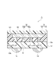
- FIG. 2 is a cross-sectional view schematically showing an example of a semiconductor device that can be manufactured by using the curable resin film 22.
- the semiconductor device 1 shown in FIG. 2 is a device having a fan-out package (FO-PKG) structure, and includes a semiconductor chip 10, a sealing portion 15 for sealing the semiconductor chip 10, a rewiring layer 13, and solder. It is equipped with a ball 14.
- the semiconductor chip 10 has a chip main body portion 10a having a first surface S1 and a second surface S2 on the opposite side thereof, and a connection terminal 10b provided on the first surface S1.
- the rewiring layer 13 is a layer for widening the terminal pitch of the connection terminals 10b, and includes, for example, an insulating layer 13a including polyimide and the like, and wiring 13b such as copper wiring.
- the terminal pitch of the connection terminal 10b is widened by the pitch conversion by the rewiring layer 13.
- the solder ball 14 is connected to a terminal whose terminal pitch is widened by the rewiring layer 13.
- the sealing portion 15 has a sealing material layer 11 that covers a portion of the surface of the semiconductor chip 10 other than the second surface S2, and a protective layer 12 that covers the second surface S2, and is on the rewiring layer 13.
- the semiconductor chip 10 is sealed with.
- the protective layer 12 can be a cured product of the curable resin film 22 according to the above-described embodiment.
- the surface S3 of the encapsulant layer 11 opposite to the rewiring layer 13 forms a flat surface together with the second surface S2 of the semiconductor chip 10, and the protective layer 12 extends so as to cover the entire flat surface. is doing.
- the protective layer 12 can be a permanent film constituting the semiconductor device without being removed after the semiconductor device is manufactured.
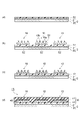
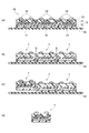
- FIGS. 3, 4 and 5 are process diagrams showing an example of a method for manufacturing the semiconductor device 1.
- the methods shown in FIGS. 3 to 5 are to form a temporary fixed laminated body 45 (FIG. 3 (d)) including the carrier 2 and the sealing structure 40 provided on the main surface of the carrier 2. This includes removing the carrier 2 from the fixed laminate 45.
- the temporary fixed laminate 45 has the curable resin film 22 and the carrier 2 bonded to each other, and the curable resin film 22 on the opposite side to the carrier 2.
- a plurality of semiconductor chips 10 are arranged on the surface so that the second surface S2 is in contact with the curable resin film 22, and the curable resin film 22 is cured to protect the curable resin film.
- the layer 12 is formed and a plurality of semiconductor chips 10 are fixed on the protective layer 12, and the encapsulant layer 11 is formed on the protective layer 12 and the semiconductor chip 10, whereby the protective layer 12 and the encapsulant are formed. It can be formed by a method including forming a sealing portion 15 having a layer 11.
- the protective film 3B may be peeled off from the film material 5 exemplified in FIG. 1, the exposed curable resin film 22 may be attached to the carrier 2, and then the support film 3A may be peeled off from the curable resin film 22.
- the curable resin film 22 and the carrier 2 may be bonded together under temperature conditions of 20 to 120 ° C.
- the "temperature condition of 20 to 120 ° C.” means a condition in which the temperature of the curable resin film 22 and the carrier 2 is within the range of 20 to 120 ° C. This temperature condition may be 40 to 100 ° C.
- the laminate of the curable resin film 22 and the carrier 2 may be pressed for bonding, and the pressure for that may be, for example, 0.01 to 1 MPa.
- the carrier 2 may have a support substrate 20 and a light absorption layer 21 provided on the main surface of the support substrate 20.
- the carrier 2 is arranged so that the light absorption layer 21 is adjacent to the curable resin film 22 or the protective layer 12 which is a cured product thereof.
- the support substrate 20 is a plate-like body that transmits the incoherent light L described later, and may be, for example, an inorganic glass substrate or a transparent resin substrate.
- the thickness of the support substrate 20 may be, for example, 0.1 to 2.0 mm.
- the light absorption layer 21 is a layer containing a conductor that absorbs incoherent light L and generates heat.
- the transmittance of the light absorption layer 21 with respect to light having a wavelength of 355 nm may be 5% or less, 3.1% or less, 3.0% or less, 2.5% or less, or 1.5% or less, and may be 0% or more. May be.
- Examples of the conductor constituting the light absorption layer 21 include metals, metal oxides, and conductive carbon materials.
- the metal may be a single metal such as chromium, copper, titanium, silver, platinum or gold, or may be an alloy such as nickel-chromium, stainless steel or copper-zinc.
- Examples of metal oxides include indium tin oxide (ITO), zinc oxide, and niobium oxide. These may be used individually by 1 type or in combination of 2 or more type.
- the conductor may be chromium, titanium, or a conductive carbon material.
- the light absorption layer 21 may be a single layer or a metal layer composed of a plurality of layers.
- the light absorbing layer 21 has thallium (Ta), platinum (Pt), nickel (Ni), titanium (Ti), tungsten (W), chromium (Cr), and the like. It may contain at least one metal selected from the group consisting of copper (Cu), aluminum (Al), silver (Ag) and gold (Au).
- the light absorption layer 21 may be composed of two layers, a first layer and a second layer, and may be laminated in the order of the first layer and the second layer from the support substrate 20 side.
- first layer has a high light absorption property
- second layer has a high coefficient of thermal expansion and a high elastic modulus
- the second layer may contain at least one metal selected from the group consisting of copper (Cu), aluminum (Al), silver (Ag) and gold (Au).
- the first layer may contain at least one metal selected from the group consisting of titanium (Ti), tungsten (W) and chromium (Cr), and the second layer may be from copper (Cu) and aluminum (Al). It may contain at least one metal selected from the group.
- the metal layer as the light absorption layer 21 may be a layer formed by physical vapor deposition (PVD) such as vacuum vapor deposition and sputtering, or chemical vapor deposition (CVD) such as plasma chemical vapor deposition, or electrolytic plating. Alternatively, it may be a plating layer formed by electroless plating.
- PVD physical vapor deposition
- CVD chemical vapor deposition
- electrolytic plating Alternatively, it may be a plating layer formed by electroless plating.
- the light absorption layer 21 may be a layer containing conductive particles that absorb light to generate heat and a binder resin in which the conductive particles are dispersed.
- the conductive particles may be particles containing the above-mentioned conductor.
- the light absorption layer 21 can be a layer containing conductive particles and a curable resin composition.
- the curable resin composition constituting the light absorption layer 21 can contain the same components as the curable resin composition constituting the curable resin film 22.
- the curable resin composition constituting the light absorption layer 21 may be the same as or different from the curable resin composition constituting the curable resin film 22.
- the content of the conductive particles in the light absorption layer 21 is 10 to 90 mass with respect to the total amount of the components other than the conductive particles in the light absorption layer 21, that is, 100 parts by mass of the binder resin or the curable resin composition. It may be a part. From the viewpoint of transmittance, the content of the conductive particles may be 20 parts by mass or more, or 30 parts by mass or more.
- the light absorbing layer containing the conductive particles and the binder resin for example, a varnish containing the conductive particles, the binder resin and the organic solvent is applied on the support member or the curable resin layer, and the organic solvent is applied from the coating film. It can be formed by methods including removal.
- the light absorption layer 21 prepared in advance may be laminated on the support substrate 20.
- the thickness of the light absorption layer 21 may be 1 to 5000 nm or 100 to 3000 nm from the viewpoint of light peelability. Further, when the thickness of the light absorption layer 21 is 50 to 300 nm, the light absorption layer 21 tends to have a sufficiently low transmittance. When the light absorption layer 21 is a single layer or a metal layer composed of a plurality of layers, the thickness of the light absorption layer 21 (or the metal layer) is 75 nm or more, 90 nm or more, or 100 nm or more from the viewpoint of good peelability. It may be present, and may be 1000 nm or less.
- the thickness of the light absorption layer 21 is 100 nm or more, 125 nm or more, 150 nm or more, or 200 nm or more from the viewpoint of good peelability. It may be 1000 nm or less. Even if the light absorption layer 21 is a metal layer containing a metal having a relatively low light absorption property (for example, Cu or Ni) or a metal layer containing a metal having a relatively low coefficient of thermal expansion (for example, Ti), the thickness thereof. The larger the value, the better the peelability tends to be obtained.
- a plurality of semiconductor chips 10 are arranged at predetermined positions on the curable resin film 22 bonded to the carrier 2 in a direction in which the second surface S2 is in contact with the curable resin film 22, that is, in a face-up direction.
- the semiconductor chip 10 may be placed on the curable resin film 22 while heating the curable resin film 22, the semiconductor chip 10, or both of them.
- the heating temperature may be, for example, 20 to 120 ° C. or 60 to 100 ° C.
- the semiconductor chip 10 placed on the curable resin film 22 may be pressurized, and the pressure for that may be 0.01 to 1.0 MPa or 0.1 to 0.2 MPa.
- the pressurization time may be, for example, 0.01 to 10 seconds or 0.1 to 2 seconds.
- the curable resin film 22 is cured by at least one of heat and light, and an integral protective layer covering the second surface S2 of all the plurality of semiconductor chips 10. 12 (cured curable resin film) is formed.
- the semiconductor chip 10 is fixed to the carrier 2 via the formed protective layer 12.
- the adhesive strength between the protective layer 12 and the carrier 2 at this point may be 1 MPa or more.
- a sealing material layer 11 for collectively sealing a plurality of semiconductor chips 10 is formed on the protective layer 12.
- the encapsulant layer 11 can be formed by using an encapsulant commonly used for encapsulating a semiconductor chip.
- the encapsulant may be a thermosetting resin composition containing an epoxy resin.
- the semiconductor chip 10 is included in the sealing portion 15 composed of the sealing material layer 11 and the protective layer 12.
- the encapsulant layer 11 is formed by a usual method such as a compression molding method. Since the semiconductor chip 10 is fixed to the protective layer 12, the position of the semiconductor chip 10 is unlikely to shift while the encapsulant layer 11 is formed.
- a part of the encapsulant layer 11 is removed by polishing from the side opposite to the protective layer 12, and the connection terminal 10b is exposed.
- the rewiring layer 13 having the wiring 13b connected to the exposed connection terminal 10b and the insulating layer 13a is formed on the encapsulant layer 11, and the encapsulant layer 11 of the rewiring layer 13 is formed.
- the sealing structure 40 including the protective layer 12 and the plurality of semiconductor chips 10 is divided on the dicing tape 50 to form the individualized semiconductor device 1, and the semiconductor device 1 is divided into the dicing tape. It may further include picking up from 50.
- the sealing structure having the semiconductor chip 10 and the sealing material layer 11 and not provided with the protective layer 12 is not supported by a carrier or the like, the interface between the semiconductor chip 10 and the sealing material layer 11 is peeled off, etc. May cause damage such as cracking.
- the protective layer 12 damage to the sealing structure separated from the carrier during the manufacturing process can be suppressed.
- the protective layer 12 can be polished, the rewiring layer 13 can be formed, and the solder balls can be formed by ordinary methods.
- the incoherent light L for separating the protective layer 12 from the carrier 2 is light that is not coherent, and is an electromagnetic wave having properties such as no interference fringes, low coherence, and low directivity. Incoherent light tends to be attenuated as the optical path length becomes longer. Laser light is generally coherent light, whereas light such as sunlight and fluorescent light is incoherent light. Incoherent light can also be said to be light excluding laser light. Since the irradiation area of the incoherent light is generally primarily wider than that of the coherent light (that is, laser light), it is possible to reduce the number of irradiations. By using incoherent light, soot is less likely to occur on the surface of the protective layer 12 exposed by peeling of the carrier 2 as compared with the case of using laser light. However, the surface of the exposed protective layer 12 may be cleaned if necessary.
- the incoherent light L may contain infrared rays.
- the incoherent light L may be pulsed light.
- the light source of the incoherent light L is not particularly limited, but may be a xenon lamp.
- a xenon lamp is a lamp that utilizes light emission by application / discharge in an arc tube filled with xenon gas.
- the irradiation conditions of the xenon lamp include the applied voltage, pulse width, irradiation time, irradiation distance (distance between the light source and the temporary fixing material layer), irradiation energy, etc., and these can be arbitrarily set according to the number of irradiations, etc. can. From the viewpoint of reducing damage to the semiconductor chip 10, irradiation conditions may be set so that the carrier 2 can be separated by one irradiation.
- a laser beam for example, a green laser
- necessary information such as a product name may be engraved on the surface of the protective layer 12 opposite to the semiconductor chip 10.
- the surface of the exposed protective layer 12 may be cleaned if necessary.
- the dicing tape 50 is attached to the protective layer 12, and the sealing portion including the plurality of semiconductor chips 10 and the protective layer 12 is included.
- the sealing structure 40 including 15, the rewiring layer 13, and the solder ball 14 is cut at a predetermined position S to form a plurality of semiconductor devices 1, and the semiconductor device 1 is cut from the dicing tape 50. It may include picking up.
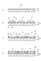
- FIGS. 6 to 8 are process diagrams showing another example of the method for manufacturing the semiconductor device 1.
- the methods shown in FIGS. 6 to 8 are to form a temporary fixed laminated body 45 (FIG. 7 (e)) including the carrier 2 and the sealing structure 40 provided on the main surface of the carrier 2. This includes removing the carrier 2 from the fixed laminate 45.
- the temporary fixing laminate 45 has a carrier 30 and a temporary fixing layer 32 provided on the carrier 30.
- the material 35 is prepared, and a plurality of semiconductor chips 10 having a chip main body portion 10a having a first surface S1 and a second surface S2 on the opposite side thereof and a connection terminal 10b provided on the second surface S2 are prepared.
- Temporary fixed laminate 45 (FIG. 6 (c)), which has a sealing material layer 11 that collectively seals on 35, and the second surface S2 of a plurality of semiconductor chips 10 is exposed from the sealing material layer 11. )) Is formed, the curable resin film 22 covering the second surface S2 and the encapsulant layer 11 is provided, the curable resin film 22 and the carrier 2 are bonded together, and the temporary fixed laminate 45 is formed. It can be formed by a method further including removing the temporary fixing material 35 from the above in this order.
- the carrier 30 constituting the temporary fixing material 35 may be, for example, a glass substrate.
- the adhesive layer 32 constituting the temporary fixing material 35 may be, for example, a release sheet having an adhesive force at room temperature and having an adhesive force decreasing by heating.
- the plurality of semiconductor chips 10 are adhered to each other in the direction in which the first surface S1 and the connection terminal 10b are located on the adhesive layer 32 side of the temporary fixing material 35, that is, in the face-down direction. Arranged on layer 32.
- the encapsulant layer 11 for encapsulating the semiconductor chip 10 is formed.
- the encapsulant layer 11 is formed so that the second surface S2 of the semiconductor chip 10 is exposed from the encapsulant layer 11.
- the encapsulant layer 11 in which the entire semiconductor chip 10 including the second surface S2 is embedded is formed, and then a part of the encapsulant layer 11 is removed by polishing from the side opposite to the temporary fixing material 35, whereby the encapsulant layer 11 is formed.
- a flat surface on which the second surface S2 of the semiconductor chip 10 is exposed may be formed.
- the temporary fixing laminate 45 at this stage is composed of a temporary fixing material 35, a plurality of semiconductor chips 10, and a sealing material layer 11.
- a curable resin film 22 covering the second surface S2 of the semiconductor chip 10 and the encapsulant layer 11 is provided, and the curing is performed as shown in FIG. 7A.
- the sex resin film 22 and the carrier 2 are bonded together.
- the carrier 2 has a support substrate 20 and a light absorption layer 21, and the light absorption layer 21 is oriented so as to be adjacent to the curable resin film 22 (or the protective layer 12), and the carrier 2 and the curable resin film 22 are attached to each other. Can be matched.
- the bonding conditions can be the same as the conditions in the method illustrated in FIG.
- the curable resin film 22 bonded to the carrier 2 may be cured to form an integral protective layer 12 (cured curable resin film) that covers the second surface S2 of all of the plurality of semiconductor chips 10. ..
- the protective layer 12 and the sealing material layer 11 form a sealing portion 15 for sealing the semiconductor chip 10 on the temporary fixing material 35.
- the sealing structure 40 has a semiconductor chip 10 and a sealing portion 15.
- the temporary fixing laminate 45 at this stage is composed of the temporary fixing material 35, the sealing structure 40, and the carrier 2.
- the temporary fixing material 35 is removed from the temporary fixing laminate 45.
- the adhesive layer 32 may be heated to separate the sealing structure 40 from the adhesive layer 32 whose adhesive strength has been reduced by heating.
- the rewiring layer 13 is formed on the exposed first surface S1.
- the rewiring layer 13 has an insulating layer 13a and wirings 13b such as copper wiring provided in the insulating layer 13a.
- a solder ball 14 is provided on the rewiring layer 13.
- the carrier 2 is removed from the temporary fixed laminated body 45 composed of the carrier 2 and the sealing structure 40.
- the method for removing the carrier 2 can be a method including irradiating the temporary fixed laminate 45 with incoherent light from the carrier 2 side, similar to the method exemplified in FIG.
- the remaining sealing structure 40 is formed by attaching the dicing tape 50 to the protective layer 12 and a plurality of semiconductor chips 10 as shown in FIGS. 8 (b) to 8 (e). ,
- the sealing structure 40 including the sealing portion 15, the rewiring layer 13, and the solder ball 14 is cut at a predetermined position S to form a plurality of semiconductor devices 1, and the semiconductor device 1 is diced with a dicing tape 50. Divided by methods including picking up from. By dividing the sealing structure 40, a semiconductor device 1 that has been made into individual pieces can be obtained.
- the cured resin film has a function of fixing the semiconductor chip during various steps such as forming a sealing material layer, thinning the semiconductor chip, and forming a rewiring layer, and sealing the semiconductor chip. It is used both for its function as a material that constitutes a part of the sealing part to be stopped. Therefore, the method according to the present disclosure can greatly simplify the manufacturing process as compared with the case where different materials are used properly for each function.
- Each varnish was applied to the support film and the coating film was dried to form 20 ⁇ m-thick curable resin films 1 to 7 on the support film.
- a protective film was placed on each curable resin film to obtain a film material composed of a support film, any of the curable resin films 1 to 7, and a protective film.
- Storage elastic modulus A plurality of curable resin films were laminated to prepare a laminated film having a thickness of about 240 ⁇ m.
- the curable resin film was cured by heating the laminated film at 130 ° C. for 20 minutes followed by heating at 170 ° C. for 2 hours.
- the dynamic viscoelasticity of the obtained cured product was measured in the range of ⁇ 80 to 300 ° C. under the following conditions using a dynamic viscoelasticity measuring device (Rheogel-E4000 manufactured by UBM). Sample size: 4 mm x 30 mm
- Tension mode frequency 10Hz
- Temperature rise rate 3 ° C./min From the obtained measurement results, the storage elastic modulus of the curable resin film after curing at 25 ° C. or 250 ° C. was determined. Table 2 shows the measurement results of shear viscosity and storage elastic modulus.
- Tackiness (90 degree peel strength)
- the curable resin film was attached to the mirror wafer or the glass substrate in an environment of 25 ° C. or while heating at 70 ° C. A pressure of 0.2 MPa was applied to the curable resin film for bonding.
- the curable resin film attached to the mirror wafer or the glass substrate was allowed to stand for 2 hours after the support tape (Oji Tape) was attached onto the curable resin film.
- the 90-degree peel strength was measured by a peeling test in which the curable resin film was peeled off in the direction of 90 degrees with respect to the main surface of the mirror wafer or the glass substrate.
- the peeling speed was 50 mm / sec. The measurement results are shown in Table 3.
- FIG. 9 is an ultraviolet-visible absorption spectrum of the curable resin films of Examples 1 and 2, and is shown here as a relative value based on the transmittance for light having a wavelength of 600 nm.
- FIG. 9 also shows the ultraviolet-visible absorption spectrum of the glass substrate.
- the curable resin film of Example 1 showed a transmittance (relative value) of 1.01% with respect to light having a wavelength of 355 nm.
- the curable resin film of Example 2 showed a transmittance of 4.76% (relative value) with respect to light having a wavelength of 355 nm.
- peeling test A carrier having a glass substrate and a light absorption layer provided on the glass substrate was prepared.
- the light absorption layer had a Ti layer (thickness: 50 ⁇ m) and a Cu layer (thickness: 200 ⁇ m), and had a laminated structure in which these were laminated in this order from the glass substrate side.
- the protective film was peeled off from the film material of the curable resin film 1 or 2, the exposed curable resin film was placed on the light absorbing layer of the carrier, and the curable resin film and the carrier were bonded together by a vacuum laminator.
- the conditions of the vacuum laminator were set to a temperature of 90 ° C., a pressure of 0.5 MPa, and a pressurization time of 60 seconds.
- a semiconductor chip for testing was placed on a curable resin film bonded to the carrier. Subsequently, the curable resin film was cured by heating at 130 ° C. for 20 minutes and then at 170 ° C. for 2 hours, whereby the semiconductor chip was fixed on the protective layer which is a cured product of the curable resin film.
- a sealing material containing an epoxy resin was used on the protective layer to form a sealing material layer for sealing the semiconductor ship at 150 ° C. for 300 seconds.
- the formed encapsulant layer was further cured by heating at 150 ° C. for 6 hours.
- a temporary fixed laminate for evaluation which was composed of a carrier, a semiconductor chip, a protective layer, and a sealing material layer, was obtained.
- the evaluation laminate was irradiated with pulsed light (incoherent light) having a width of 300 ⁇ m from the glass substrate side with a xenon lamp having a voltage of 750 V.
- pulsed light incoherent light
- the carriers spontaneously peeled from the protective layer after irradiation with the pulsed light without requiring stress. No soot was found on the surface of the exposed protective layer.
Landscapes
- Encapsulation Of And Coatings For Semiconductor Or Solid State Devices (AREA)
- Laminated Bodies (AREA)
Priority Applications (4)
| Application Number | Priority Date | Filing Date | Title |
|---|---|---|---|
| KR1020237019189A KR20230113759A (ko) | 2020-12-04 | 2021-12-03 | 반도체 장치를 제조하는 방법 |
| CN202180081462.9A CN116547800A (zh) | 2020-12-04 | 2021-12-03 | 制造半导体装置的方法 |
| US18/255,367 US20240006192A1 (en) | 2020-12-04 | 2021-12-03 | Method for manufacturing semiconductor device |
| JP2022567012A JP7845191B2 (ja) | 2020-12-04 | 2021-12-03 | 半導体装置を製造する方法 |
Applications Claiming Priority (2)
| Application Number | Priority Date | Filing Date | Title |
|---|---|---|---|
| JPPCT/JP2020/045336 | 2020-12-04 | ||
| JP2020045336 | 2020-12-04 |
Publications (1)
| Publication Number | Publication Date |
|---|---|
| WO2022118971A1 true WO2022118971A1 (ja) | 2022-06-09 |
Family
ID=81853336
Family Applications (1)
| Application Number | Title | Priority Date | Filing Date |
|---|---|---|---|
| PCT/JP2021/044561 Ceased WO2022118971A1 (ja) | 2020-12-04 | 2021-12-03 | 半導体装置を製造する方法 |
Country Status (5)
| Country | Link |
|---|---|
| US (1) | US20240006192A1 (https=) |
| JP (1) | JP7845191B2 (https=) |
| KR (1) | KR20230113759A (https=) |
| CN (1) | CN116547800A (https=) |
| WO (1) | WO2022118971A1 (https=) |
Families Citing this family (4)
| Publication number | Priority date | Publication date | Assignee | Title |
|---|---|---|---|---|
| US11996384B2 (en) | 2020-12-15 | 2024-05-28 | Pulseforge, Inc. | Method and apparatus for debonding temporarily bonded wafers in wafer-level packaging applications |
| CN116888714A (zh) * | 2021-02-01 | 2023-10-13 | 长濑化成株式会社 | 电子部件安装基板的密封方法及热固化性片材 |
| WO2025061255A1 (de) * | 2023-09-18 | 2025-03-27 | Erich Thallner | Substratstapel, modifiziertes schichtsystem, verfahren zum handhaben des substratstapels und vorrichtung für ein solches verfahren |
| CN121816100A (zh) * | 2026-03-11 | 2026-04-07 | 北京升宇科技有限公司 | 微型高可靠封装结构及其制备方法 |
Citations (5)
| Publication number | Priority date | Publication date | Assignee | Title |
|---|---|---|---|---|
| JP2006222164A (ja) * | 2005-02-08 | 2006-08-24 | Shinko Electric Ind Co Ltd | 半導体装置及びその製造方法 |
| JP2013074184A (ja) * | 2011-09-28 | 2013-04-22 | Nitto Denko Corp | 半導体装置の製造方法 |
| JP2016139754A (ja) * | 2015-01-29 | 2016-08-04 | 日立化成株式会社 | 半導体装置の製造方法 |
| JP2018009138A (ja) * | 2016-07-05 | 2018-01-18 | 日立化成株式会社 | 仮固定用樹脂組成物、仮固定用樹脂フィルム及び仮固定用樹脂フィルムシート |
| JP2020105276A (ja) * | 2018-12-26 | 2020-07-09 | 東京応化工業株式会社 | 接着剤組成物、積層体、積層体の製造方法、及び電子部品の製造方法 |
Family Cites Families (3)
| Publication number | Priority date | Publication date | Assignee | Title |
|---|---|---|---|---|
| JP3853247B2 (ja) | 2002-04-16 | 2006-12-06 | 日東電工株式会社 | 電子部品用加熱剥離型粘着シートおよび電子部品の加工方法並びに電子部品 |
| KR101058621B1 (ko) * | 2009-07-23 | 2011-08-22 | 삼성전기주식회사 | 반도체 패키지 및 이의 제조 방법 |
| JP2016048729A (ja) * | 2014-08-27 | 2016-04-07 | 株式会社東芝 | 仮接着用支持基板及び半導体デバイスの製造方法 |
-
2021
- 2021-12-03 CN CN202180081462.9A patent/CN116547800A/zh active Pending
- 2021-12-03 JP JP2022567012A patent/JP7845191B2/ja active Active
- 2021-12-03 WO PCT/JP2021/044561 patent/WO2022118971A1/ja not_active Ceased
- 2021-12-03 KR KR1020237019189A patent/KR20230113759A/ko active Pending
- 2021-12-03 US US18/255,367 patent/US20240006192A1/en active Pending
Patent Citations (5)
| Publication number | Priority date | Publication date | Assignee | Title |
|---|---|---|---|---|
| JP2006222164A (ja) * | 2005-02-08 | 2006-08-24 | Shinko Electric Ind Co Ltd | 半導体装置及びその製造方法 |
| JP2013074184A (ja) * | 2011-09-28 | 2013-04-22 | Nitto Denko Corp | 半導体装置の製造方法 |
| JP2016139754A (ja) * | 2015-01-29 | 2016-08-04 | 日立化成株式会社 | 半導体装置の製造方法 |
| JP2018009138A (ja) * | 2016-07-05 | 2018-01-18 | 日立化成株式会社 | 仮固定用樹脂組成物、仮固定用樹脂フィルム及び仮固定用樹脂フィルムシート |
| JP2020105276A (ja) * | 2018-12-26 | 2020-07-09 | 東京応化工業株式会社 | 接着剤組成物、積層体、積層体の製造方法、及び電子部品の製造方法 |
Also Published As
| Publication number | Publication date |
|---|---|
| KR20230113759A (ko) | 2023-08-01 |
| TW202230613A (zh) | 2022-08-01 |
| JPWO2022118971A1 (https=) | 2022-06-09 |
| JP7845191B2 (ja) | 2026-04-14 |
| CN116547800A (zh) | 2023-08-04 |
| US20240006192A1 (en) | 2024-01-04 |
Similar Documents
| Publication | Publication Date | Title |
|---|---|---|
| JP7845191B2 (ja) | 半導体装置を製造する方法 | |
| JP5544766B2 (ja) | 半導体加工用接着フィルム積層体 | |
| CN102598235B (zh) | 半导体接合用粘接剂、半导体接合用粘接膜、半导体芯片的安装方法及半导体装置 | |
| JP4872587B2 (ja) | 封止フィルム、及びこれを用いた半導体装置 | |
| JP5569126B2 (ja) | 接着剤組成物、接着剤シート及び半導体装置の製造方法 | |
| JP2012124466A (ja) | 半導体装置用接着フィルム、及び、半導体装置 | |
| JP7226664B2 (ja) | 半導体装置の製造方法 | |
| JP2016119493A (ja) | ダイボンドフィルム、ダイシング・ダイボンドフィルム、ダイボンドフィルムの製造方法、及び、ダイボンドフィルムを有する半導体装置 | |
| WO2017047183A1 (ja) | 半導体裏面用フィルム | |
| JP4893640B2 (ja) | 半導体用接着フィルム及びこれを用いた半導体装置 | |
| JP5397243B2 (ja) | 半導体装置の製造方法及び回路部材接続用接着シート | |
| JP2006269887A (ja) | 半導体用接着フィルム及びこれを用いた半導体装置 | |
| Saiki et al. | UV/heat dual‐curable adhesive tapes for fabricating stacked packages of semiconductors | |
| JP7845190B2 (ja) | 硬化性樹脂フィルム、半導体装置製造用フィルム材、半導体装置製造用硬化性樹脂組成物、及び、半導体装置を製造する方法 | |
| JP4050290B2 (ja) | 半導体用接着フィルム及びこれを用いた半導体装置 | |
| TWI918789B (zh) | 製造半導體裝置之方法 | |
| JP2023054825A (ja) | 半導体装置の製造方法 | |
| JP2023107769A (ja) | 樹脂シート、樹脂シートの使用方法、及び硬化樹脂層付き硬化封止体の製造方法 | |
| KR20230166071A (ko) | 반도체용 접착제, 반도체용 접착제 시트, 및 반도체장치의 제조 방법 | |
| JP5375351B2 (ja) | 半導体回路部材の製造方法 | |
| JP2026020760A (ja) | 保護膜形成フィルム、及び保護膜付きワーク加工物の製造方法 | |
| JP2025144308A (ja) | 保護膜形成フィルム、及び保護膜付きワーク加工物の製造方法 | |
| JP2025030776A (ja) | 硬化性樹脂フィルム複合シート及び硬化封止体の製造方法 | |
| WO2019098326A1 (ja) | 第1保護膜付き半導体チップ、第1保護膜付き半導体チップの製造方法、及び半導体チップ・第1保護膜積層体の評価方法 |
Legal Events
| Date | Code | Title | Description |
|---|---|---|---|
| 121 | Ep: the epo has been informed by wipo that ep was designated in this application |
Ref document number: 21900720 Country of ref document: EP Kind code of ref document: A1 |
|
| ENP | Entry into the national phase |
Ref document number: 2022567012 Country of ref document: JP Kind code of ref document: A |
|
| WWE | Wipo information: entry into national phase |
Ref document number: 18255367 Country of ref document: US |
|
| WWE | Wipo information: entry into national phase |
Ref document number: 202180081462.9 Country of ref document: CN |
|
| ENP | Entry into the national phase |
Ref document number: 20237019189 Country of ref document: KR Kind code of ref document: A |
|
| NENP | Non-entry into the national phase |
Ref country code: DE |
|
| 122 | Ep: pct application non-entry in european phase |
Ref document number: 21900720 Country of ref document: EP Kind code of ref document: A1 |