KR20230113759A - 반도체 장치를 제조하는 방법 - Google Patents
반도체 장치를 제조하는 방법 Download PDFInfo
- Publication number
- KR20230113759A KR20230113759A KR1020237019189A KR20237019189A KR20230113759A KR 20230113759 A KR20230113759 A KR 20230113759A KR 1020237019189 A KR1020237019189 A KR 1020237019189A KR 20237019189 A KR20237019189 A KR 20237019189A KR 20230113759 A KR20230113759 A KR 20230113759A
- Authority
- KR
- South Korea
- Prior art keywords
- curable resin
- resin film
- carrier
- layer
- temporarily fixed
- Prior art date
- Legal status (The legal status is an assumption and is not a legal conclusion. Google has not performed a legal analysis and makes no representation as to the accuracy of the status listed.)
- Pending
Links
Images


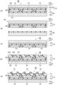


Classifications
-
- H—ELECTRICITY
- H10—SEMICONDUCTOR DEVICES; ELECTRIC SOLID-STATE DEVICES NOT OTHERWISE PROVIDED FOR
- H10P—GENERIC PROCESSES OR APPARATUS FOR THE MANUFACTURE OR TREATMENT OF DEVICES COVERED BY CLASS H10
- H10P72/00—Handling or holding of wafers, substrates or devices during manufacture or treatment thereof
- H10P72/70—Handling or holding of wafers, substrates or devices during manufacture or treatment thereof for supporting or gripping
- H10P72/74—Handling or holding of wafers, substrates or devices during manufacture or treatment thereof for supporting or gripping using temporarily an auxiliary support
-
- H—ELECTRICITY
- H10—SEMICONDUCTOR DEVICES; ELECTRIC SOLID-STATE DEVICES NOT OTHERWISE PROVIDED FOR
- H10W—GENERIC PACKAGES, INTERCONNECTIONS, CONNECTORS OR OTHER CONSTRUCTIONAL DETAILS OF DEVICES COVERED BY CLASS H10
- H10W74/00—Encapsulations, e.g. protective coatings
- H10W74/01—Manufacture or treatment
- H10W74/019—Manufacture or treatment using temporary auxiliary substrates
-
- H01L21/568—
-
- H01L21/561—
-
- H01L21/6835—
-
- H01L21/78—
-
- H01L23/3128—
-
- H01L23/544—
-
- H01L23/562—
-
- H—ELECTRICITY
- H10—SEMICONDUCTOR DEVICES; ELECTRIC SOLID-STATE DEVICES NOT OTHERWISE PROVIDED FOR
- H10P—GENERIC PROCESSES OR APPARATUS FOR THE MANUFACTURE OR TREATMENT OF DEVICES COVERED BY CLASS H10
- H10P54/00—Cutting or separating of wafers, substrates or parts of devices
-
- H—ELECTRICITY
- H10—SEMICONDUCTOR DEVICES; ELECTRIC SOLID-STATE DEVICES NOT OTHERWISE PROVIDED FOR
- H10P—GENERIC PROCESSES OR APPARATUS FOR THE MANUFACTURE OR TREATMENT OF DEVICES COVERED BY CLASS H10
- H10P72/00—Handling or holding of wafers, substrates or devices during manufacture or treatment thereof
- H10P72/70—Handling or holding of wafers, substrates or devices during manufacture or treatment thereof for supporting or gripping
- H10P72/74—Handling or holding of wafers, substrates or devices during manufacture or treatment thereof for supporting or gripping using temporarily an auxiliary support
- H10P72/7412—Handling or holding of wafers, substrates or devices during manufacture or treatment thereof for supporting or gripping using temporarily an auxiliary support the auxiliary support including means facilitating the separation of a device or wafer from the auxiliary support
-
- H—ELECTRICITY
- H10—SEMICONDUCTOR DEVICES; ELECTRIC SOLID-STATE DEVICES NOT OTHERWISE PROVIDED FOR
- H10P—GENERIC PROCESSES OR APPARATUS FOR THE MANUFACTURE OR TREATMENT OF DEVICES COVERED BY CLASS H10
- H10P72/00—Handling or holding of wafers, substrates or devices during manufacture or treatment thereof
- H10P72/70—Handling or holding of wafers, substrates or devices during manufacture or treatment thereof for supporting or gripping
- H10P72/74—Handling or holding of wafers, substrates or devices during manufacture or treatment thereof for supporting or gripping using temporarily an auxiliary support
- H10P72/744—Details of chemical or physical process used for separating the auxiliary support from a device or a wafer
-
- H—ELECTRICITY
- H10—SEMICONDUCTOR DEVICES; ELECTRIC SOLID-STATE DEVICES NOT OTHERWISE PROVIDED FOR
- H10W—GENERIC PACKAGES, INTERCONNECTIONS, CONNECTORS OR OTHER CONSTRUCTIONAL DETAILS OF DEVICES COVERED BY CLASS H10
- H10W42/00—Arrangements for protection of devices
- H10W42/121—Arrangements for protection of devices protecting against mechanical damage
-
- H—ELECTRICITY
- H10—SEMICONDUCTOR DEVICES; ELECTRIC SOLID-STATE DEVICES NOT OTHERWISE PROVIDED FOR
- H10W—GENERIC PACKAGES, INTERCONNECTIONS, CONNECTORS OR OTHER CONSTRUCTIONAL DETAILS OF DEVICES COVERED BY CLASS H10
- H10W46/00—Marks applied to devices, e.g. for alignment or identification
-
- H—ELECTRICITY
- H10—SEMICONDUCTOR DEVICES; ELECTRIC SOLID-STATE DEVICES NOT OTHERWISE PROVIDED FOR
- H10W—GENERIC PACKAGES, INTERCONNECTIONS, CONNECTORS OR OTHER CONSTRUCTIONAL DETAILS OF DEVICES COVERED BY CLASS H10
- H10W70/00—Package substrates; Interposers; Redistribution layers [RDL]
- H10W70/60—Insulating or insulated package substrates; Interposers; Redistribution layers
-
- H—ELECTRICITY
- H10—SEMICONDUCTOR DEVICES; ELECTRIC SOLID-STATE DEVICES NOT OTHERWISE PROVIDED FOR
- H10W—GENERIC PACKAGES, INTERCONNECTIONS, CONNECTORS OR OTHER CONSTRUCTIONAL DETAILS OF DEVICES COVERED BY CLASS H10
- H10W74/00—Encapsulations, e.g. protective coatings
- H10W74/01—Manufacture or treatment
- H10W74/014—Manufacture or treatment using batch processing
-
- H—ELECTRICITY
- H10—SEMICONDUCTOR DEVICES; ELECTRIC SOLID-STATE DEVICES NOT OTHERWISE PROVIDED FOR
- H10W—GENERIC PACKAGES, INTERCONNECTIONS, CONNECTORS OR OTHER CONSTRUCTIONAL DETAILS OF DEVICES COVERED BY CLASS H10
- H10W74/00—Encapsulations, e.g. protective coatings
- H10W74/10—Encapsulations, e.g. protective coatings characterised by their shape or disposition
- H10W74/111—Encapsulations, e.g. protective coatings characterised by their shape or disposition the semiconductor body being completely enclosed
- H10W74/114—Encapsulations, e.g. protective coatings characterised by their shape or disposition the semiconductor body being completely enclosed by a substrate and the encapsulations
- H10W74/117—Encapsulations, e.g. protective coatings characterised by their shape or disposition the semiconductor body being completely enclosed by a substrate and the encapsulations the substrate having spherical bumps for external connection
-
- H01L2221/68318—
-
- H01L2221/68381—
-
- H—ELECTRICITY
- H10—SEMICONDUCTOR DEVICES; ELECTRIC SOLID-STATE DEVICES NOT OTHERWISE PROVIDED FOR
- H10P—GENERIC PROCESSES OR APPARATUS FOR THE MANUFACTURE OR TREATMENT OF DEVICES COVERED BY CLASS H10
- H10P72/00—Handling or holding of wafers, substrates or devices during manufacture or treatment thereof
- H10P72/70—Handling or holding of wafers, substrates or devices during manufacture or treatment thereof for supporting or gripping
- H10P72/74—Handling or holding of wafers, substrates or devices during manufacture or treatment thereof for supporting or gripping using temporarily an auxiliary support
- H10P72/7424—Handling or holding of wafers, substrates or devices during manufacture or treatment thereof for supporting or gripping using temporarily an auxiliary support used as a support during the manufacture of self-supporting substrates
Landscapes
- Encapsulation Of And Coatings For Semiconductor Or Solid State Devices (AREA)
- Laminated Bodies (AREA)
Applications Claiming Priority (3)
| Application Number | Priority Date | Filing Date | Title |
|---|---|---|---|
| JPPCT/JP2020/045336 | 2020-12-04 | ||
| JP2020045336 | 2020-12-04 | ||
| PCT/JP2021/044561 WO2022118971A1 (ja) | 2020-12-04 | 2021-12-03 | 半導体装置を製造する方法 |
Publications (1)
| Publication Number | Publication Date |
|---|---|
| KR20230113759A true KR20230113759A (ko) | 2023-08-01 |
Family
ID=81853336
Family Applications (1)
| Application Number | Title | Priority Date | Filing Date |
|---|---|---|---|
| KR1020237019189A Pending KR20230113759A (ko) | 2020-12-04 | 2021-12-03 | 반도체 장치를 제조하는 방법 |
Country Status (5)
| Country | Link |
|---|---|
| US (1) | US20240006192A1 (https=) |
| JP (1) | JP7845191B2 (https=) |
| KR (1) | KR20230113759A (https=) |
| CN (1) | CN116547800A (https=) |
| WO (1) | WO2022118971A1 (https=) |
Cited By (1)
| Publication number | Priority date | Publication date | Assignee | Title |
|---|---|---|---|---|
| WO2025061255A1 (de) * | 2023-09-18 | 2025-03-27 | Erich Thallner | Substratstapel, modifiziertes schichtsystem, verfahren zum handhaben des substratstapels und vorrichtung für ein solches verfahren |
Families Citing this family (3)
| Publication number | Priority date | Publication date | Assignee | Title |
|---|---|---|---|---|
| US11996384B2 (en) | 2020-12-15 | 2024-05-28 | Pulseforge, Inc. | Method and apparatus for debonding temporarily bonded wafers in wafer-level packaging applications |
| CN116888714A (zh) * | 2021-02-01 | 2023-10-13 | 长濑化成株式会社 | 电子部件安装基板的密封方法及热固化性片材 |
| CN121816100A (zh) * | 2026-03-11 | 2026-04-07 | 北京升宇科技有限公司 | 微型高可靠封装结构及其制备方法 |
Citations (1)
| Publication number | Priority date | Publication date | Assignee | Title |
|---|---|---|---|---|
| JP2003306653A (ja) | 2002-04-16 | 2003-10-31 | Nitto Denko Corp | 電子部品用加熱剥離型粘着シートおよび電子部品の加工方法並びに電子部品 |
Family Cites Families (7)
| Publication number | Priority date | Publication date | Assignee | Title |
|---|---|---|---|---|
| JP2006222164A (ja) * | 2005-02-08 | 2006-08-24 | Shinko Electric Ind Co Ltd | 半導体装置及びその製造方法 |
| KR101058621B1 (ko) * | 2009-07-23 | 2011-08-22 | 삼성전기주식회사 | 반도체 패키지 및 이의 제조 방법 |
| JP2013074184A (ja) * | 2011-09-28 | 2013-04-22 | Nitto Denko Corp | 半導体装置の製造方法 |
| JP2016048729A (ja) * | 2014-08-27 | 2016-04-07 | 株式会社東芝 | 仮接着用支持基板及び半導体デバイスの製造方法 |
| JP2016139754A (ja) * | 2015-01-29 | 2016-08-04 | 日立化成株式会社 | 半導体装置の製造方法 |
| JP6859729B2 (ja) * | 2016-07-05 | 2021-04-14 | 昭和電工マテリアルズ株式会社 | 仮固定用樹脂組成物、仮固定用樹脂フィルム、仮固定用樹脂フィルムシート及び半導体装置の製造方法 |
| JP7221046B2 (ja) * | 2018-12-26 | 2023-02-13 | 東京応化工業株式会社 | 接着剤組成物、積層体、積層体の製造方法、及び電子部品の製造方法 |
-
2021
- 2021-12-03 CN CN202180081462.9A patent/CN116547800A/zh active Pending
- 2021-12-03 JP JP2022567012A patent/JP7845191B2/ja active Active
- 2021-12-03 WO PCT/JP2021/044561 patent/WO2022118971A1/ja not_active Ceased
- 2021-12-03 KR KR1020237019189A patent/KR20230113759A/ko active Pending
- 2021-12-03 US US18/255,367 patent/US20240006192A1/en active Pending
Patent Citations (1)
| Publication number | Priority date | Publication date | Assignee | Title |
|---|---|---|---|---|
| JP2003306653A (ja) | 2002-04-16 | 2003-10-31 | Nitto Denko Corp | 電子部品用加熱剥離型粘着シートおよび電子部品の加工方法並びに電子部品 |
Cited By (1)
| Publication number | Priority date | Publication date | Assignee | Title |
|---|---|---|---|---|
| WO2025061255A1 (de) * | 2023-09-18 | 2025-03-27 | Erich Thallner | Substratstapel, modifiziertes schichtsystem, verfahren zum handhaben des substratstapels und vorrichtung für ein solches verfahren |
Also Published As
| Publication number | Publication date |
|---|---|
| TW202230613A (zh) | 2022-08-01 |
| JPWO2022118971A1 (https=) | 2022-06-09 |
| JP7845191B2 (ja) | 2026-04-14 |
| CN116547800A (zh) | 2023-08-04 |
| WO2022118971A1 (ja) | 2022-06-09 |
| US20240006192A1 (en) | 2024-01-04 |
Similar Documents
| Publication | Publication Date | Title |
|---|---|---|
| KR20230113759A (ko) | 반도체 장치를 제조하는 방법 | |
| CN102002323B (zh) | 带有切割片的胶粘薄膜及其制造方法 | |
| CN102061136B (zh) | 树脂密封用粘合带及树脂密封型半导体装置的制造方法 | |
| JP5569126B2 (ja) | 接着剤組成物、接着剤シート及び半導体装置の製造方法 | |
| JP5544766B2 (ja) | 半導体加工用接着フィルム積層体 | |
| JP4872587B2 (ja) | 封止フィルム、及びこれを用いた半導体装置 | |
| KR20110019408A (ko) | 열경화형 다이본드 필름 | |
| JP7226664B2 (ja) | 半導体装置の製造方法 | |
| JP2011140617A (ja) | アンダーフィル形成用接着剤組成物、アンダーフィル形成用接着剤シート及び半導体装置の製造方法 | |
| WO2007102482A1 (ja) | 実装方法、電気部品付き基板及び電気装置 | |
| KR20120030443A (ko) | 접착제 조성물, 회로 부재 접속용 접착제 시트 및 반도체 장치의 제조 방법 | |
| JP5397243B2 (ja) | 半導体装置の製造方法及び回路部材接続用接着シート | |
| JP6608147B2 (ja) | 多層接着フィルム、および接続構造体 | |
| KR20230117136A (ko) | 경화성 수지 필름, 반도체 장치 제조용 필름재, 반도체 장치 제조용 경화성 수지 조성물, 및, 반도체 장치를 제조하는 방법 | |
| JP4050290B2 (ja) | 半導体用接着フィルム及びこれを用いた半導体装置 | |
| JP7226669B2 (ja) | 半導体装置の製造方法 | |
| KR20230166071A (ko) | 반도체용 접착제, 반도체용 접착제 시트, 및 반도체장치의 제조 방법 | |
| JP2006206787A (ja) | ダイシングシート機能付きダイアタッチフィルム及びそれを用いた半導体装置の製造方法及び半導体装置。 | |
| JP5375351B2 (ja) | 半導体回路部材の製造方法 | |
| JP2007073647A (ja) | ダイシングシート機能付きダイアタッチフィルム及びそれを用いた半導体装置の製造方法及び半導体装置。 | |
| CN103715124A (zh) | 利用响应于能量射线的耐热粘合片制造半导体器件的方法 | |
| TWI916458B (zh) | 半導體裝置之製造方法 | |
| SG174368A1 (en) | Spacer formation film, semiconductor wafer and semiconductor device | |
| KR20250030402A (ko) | 경화성 수지 필름, 경화 봉지체의 제조 방법, 경화성 수지 필름 복합 시트 및 경화 봉지체 | |
| KR20260024969A (ko) | 반도체 장치의 제조 방법 및 가고정용 적층체 |
Legal Events
| Date | Code | Title | Description |
|---|---|---|---|
| PA0105 | International application |
St.27 status event code: A-0-1-A10-A15-nap-PA0105 |
|
| PG1501 | Laying open of application |
St.27 status event code: A-1-1-Q10-Q12-nap-PG1501 |
|
| R18-X000 | Changes to party contact information recorded |
St.27 status event code: A-3-3-R10-R18-oth-X000 |
|
| A201 | Request for examination | ||
| PA0201 | Request for examination |
St.27 status event code: A-1-2-D10-D11-exm-PA0201 |
|
| D21 | Rejection of application intended |
Free format text: ST27 STATUS EVENT CODE: A-1-2-D10-D21-EXM-PE0902 (AS PROVIDED BY THE NATIONAL OFFICE) |
|
| PE0902 | Notice of grounds for rejection |
St.27 status event code: A-1-2-D10-D21-exm-PE0902 |
|
| P22-X000 | Classification modified |
St.27 status event code: A-2-2-P10-P22-nap-X000 |
|
| P22-X000 | Classification modified |
St.27 status event code: A-2-2-P10-P22-nap-X000 |
|
| E13 | Pre-grant limitation requested |
Free format text: ST27 STATUS EVENT CODE: A-2-3-E10-E13-LIM-X000 (AS PROVIDED BY THE NATIONAL OFFICE) |
|
| E13-X000 | Pre-grant limitation requested |
St.27 status event code: A-2-3-E10-E13-lim-X000 |
|
| P11 | Amendment of application requested |
Free format text: ST27 STATUS EVENT CODE: A-2-2-P10-P11-NAP-X000 (AS PROVIDED BY THE NATIONAL OFFICE) |
|
| P11-X000 | Amendment of application requested |
St.27 status event code: A-2-2-P10-P11-nap-X000 |