WO2022106953A1 - 半導体装置、及び半導体装置の作製方法 - Google Patents
半導体装置、及び半導体装置の作製方法 Download PDFInfo
- Publication number
- WO2022106953A1 WO2022106953A1 PCT/IB2021/060296 IB2021060296W WO2022106953A1 WO 2022106953 A1 WO2022106953 A1 WO 2022106953A1 IB 2021060296 W IB2021060296 W IB 2021060296W WO 2022106953 A1 WO2022106953 A1 WO 2022106953A1
- Authority
- WO
- WIPO (PCT)
- Prior art keywords
- layer
- insulating layer
- conductive layer
- transistor
- semiconductor
- Prior art date
Links
- 239000004065 semiconductor Substances 0.000 title claims abstract description 562
- 238000004519 manufacturing process Methods 0.000 title claims abstract description 59
- 239000000758 substrate Substances 0.000 claims abstract description 150
- 238000000034 method Methods 0.000 claims abstract description 130
- 238000012545 processing Methods 0.000 claims description 33
- 238000009413 insulation Methods 0.000 abstract description 20
- 239000010410 layer Substances 0.000 description 1746
- 239000010408 film Substances 0.000 description 349
- 229910052760 oxygen Inorganic materials 0.000 description 166
- 239000001301 oxygen Substances 0.000 description 166
- QVGXLLKOCUKJST-UHFFFAOYSA-N atomic oxygen Chemical compound [O] QVGXLLKOCUKJST-UHFFFAOYSA-N 0.000 description 165
- 229910044991 metal oxide Inorganic materials 0.000 description 137
- 150000004706 metal oxides Chemical class 0.000 description 137
- 239000011701 zinc Substances 0.000 description 127
- 239000007789 gas Substances 0.000 description 90
- 230000006870 function Effects 0.000 description 82
- 239000004973 liquid crystal related substance Substances 0.000 description 64
- MWUXSHHQAYIFBG-UHFFFAOYSA-N nitrogen oxide Inorganic materials O=[N] MWUXSHHQAYIFBG-UHFFFAOYSA-N 0.000 description 61
- 239000001257 hydrogen Substances 0.000 description 54
- 229910052739 hydrogen Inorganic materials 0.000 description 54
- 239000000463 material Substances 0.000 description 53
- QGZKDVFQNNGYKY-UHFFFAOYSA-N Ammonia Chemical compound N QGZKDVFQNNGYKY-UHFFFAOYSA-N 0.000 description 50
- 230000015572 biosynthetic process Effects 0.000 description 50
- 238000010438 heat treatment Methods 0.000 description 44
- 239000012298 atmosphere Substances 0.000 description 43
- 238000009832 plasma treatment Methods 0.000 description 43
- XLYOFNOQVPJJNP-UHFFFAOYSA-N water Substances O XLYOFNOQVPJJNP-UHFFFAOYSA-N 0.000 description 40
- 229910001868 water Inorganic materials 0.000 description 40
- UFHFLCQGNIYNRP-UHFFFAOYSA-N Hydrogen Chemical compound [H][H] UFHFLCQGNIYNRP-UHFFFAOYSA-N 0.000 description 34
- 238000004140 cleaning Methods 0.000 description 34
- 229910052581 Si3N4 Inorganic materials 0.000 description 33
- 229910052814 silicon oxide Inorganic materials 0.000 description 32
- VYPSYNLAJGMNEJ-UHFFFAOYSA-N Silicium dioxide Chemical compound O=[Si]=O VYPSYNLAJGMNEJ-UHFFFAOYSA-N 0.000 description 29
- 239000012535 impurity Substances 0.000 description 29
- HQVNEWCFYHHQES-UHFFFAOYSA-N silicon nitride Chemical compound N12[Si]34N5[Si]62N3[Si]51N64 HQVNEWCFYHHQES-UHFFFAOYSA-N 0.000 description 28
- IJGRMHOSHXDMSA-UHFFFAOYSA-N Atomic nitrogen Chemical compound N#N IJGRMHOSHXDMSA-UHFFFAOYSA-N 0.000 description 25
- 238000004544 sputter deposition Methods 0.000 description 25
- 230000001590 oxidative effect Effects 0.000 description 24
- 230000008569 process Effects 0.000 description 24
- 229910052751 metal Inorganic materials 0.000 description 23
- GQPLMRYTRLFLPF-UHFFFAOYSA-N Nitrous Oxide Chemical group [O-][N+]#N GQPLMRYTRLFLPF-UHFFFAOYSA-N 0.000 description 22
- 229910021529 ammonia Inorganic materials 0.000 description 22
- 239000013078 crystal Substances 0.000 description 22
- 230000007547 defect Effects 0.000 description 22
- 239000002184 metal Substances 0.000 description 22
- 239000000203 mixture Substances 0.000 description 21
- 239000004020 conductor Substances 0.000 description 20
- 150000002431 hydrogen Chemical class 0.000 description 20
- 230000001603 reducing effect Effects 0.000 description 20
- 238000009792 diffusion process Methods 0.000 description 19
- 230000001965 increasing effect Effects 0.000 description 18
- 229910052738 indium Inorganic materials 0.000 description 18
- 239000011347 resin Substances 0.000 description 18
- 229920005989 resin Polymers 0.000 description 18
- 238000005477 sputtering target Methods 0.000 description 18
- RYGMFSIKBFXOCR-UHFFFAOYSA-N Copper Chemical compound [Cu] RYGMFSIKBFXOCR-UHFFFAOYSA-N 0.000 description 17
- 229910052782 aluminium Inorganic materials 0.000 description 17
- XAGFODPZIPBFFR-UHFFFAOYSA-N aluminium Chemical compound [Al] XAGFODPZIPBFFR-UHFFFAOYSA-N 0.000 description 17
- 229910052802 copper Inorganic materials 0.000 description 17
- 239000010949 copper Substances 0.000 description 17
- APFVFJFRJDLVQX-UHFFFAOYSA-N indium atom Chemical compound [In] APFVFJFRJDLVQX-UHFFFAOYSA-N 0.000 description 16
- 239000010409 thin film Substances 0.000 description 16
- XUIMIQQOPSSXEZ-UHFFFAOYSA-N Silicon Chemical compound [Si] XUIMIQQOPSSXEZ-UHFFFAOYSA-N 0.000 description 15
- 229910052710 silicon Inorganic materials 0.000 description 15
- 239000010703 silicon Substances 0.000 description 15
- MYMOFIZGZYHOMD-UHFFFAOYSA-N Dioxygen Chemical compound O=O MYMOFIZGZYHOMD-UHFFFAOYSA-N 0.000 description 14
- 229910001882 dioxygen Inorganic materials 0.000 description 14
- 229910052733 gallium Inorganic materials 0.000 description 14
- 239000011241 protective layer Substances 0.000 description 14
- -1 silicon nitride nitride Chemical class 0.000 description 14
- 238000000623 plasma-assisted chemical vapour deposition Methods 0.000 description 13
- GYHNNYVSQQEPJS-UHFFFAOYSA-N Gallium Chemical compound [Ga] GYHNNYVSQQEPJS-UHFFFAOYSA-N 0.000 description 12
- 206010021143 Hypoxia Diseases 0.000 description 12
- 229910052757 nitrogen Inorganic materials 0.000 description 12
- PMHQVHHXPFUNSP-UHFFFAOYSA-M copper(1+);methylsulfanylmethane;bromide Chemical compound Br[Cu].CSC PMHQVHHXPFUNSP-UHFFFAOYSA-M 0.000 description 11
- 238000005530 etching Methods 0.000 description 11
- 150000004767 nitrides Chemical class 0.000 description 11
- TWNQGVIAIRXVLR-UHFFFAOYSA-N oxo(oxoalumanyloxy)alumane Chemical compound O=[Al]O[Al]=O TWNQGVIAIRXVLR-UHFFFAOYSA-N 0.000 description 11
- 229910045601 alloy Inorganic materials 0.000 description 10
- 239000000956 alloy Substances 0.000 description 10
- 230000004888 barrier function Effects 0.000 description 10
- 239000012528 membrane Substances 0.000 description 10
- 230000003287 optical effect Effects 0.000 description 10
- HCHKCACWOHOZIP-UHFFFAOYSA-N Zinc Chemical compound [Zn] HCHKCACWOHOZIP-UHFFFAOYSA-N 0.000 description 9
- 238000005229 chemical vapour deposition Methods 0.000 description 9
- 230000007812 deficiency Effects 0.000 description 9
- 239000011521 glass Substances 0.000 description 9
- 229910000449 hafnium oxide Inorganic materials 0.000 description 9
- WIHZLLGSGQNAGK-UHFFFAOYSA-N hafnium(4+);oxygen(2-) Chemical compound [O-2].[O-2].[Hf+4] WIHZLLGSGQNAGK-UHFFFAOYSA-N 0.000 description 9
- 239000011810 insulating material Substances 0.000 description 9
- WFKWXMTUELFFGS-UHFFFAOYSA-N tungsten Chemical compound [W] WFKWXMTUELFFGS-UHFFFAOYSA-N 0.000 description 9
- 229910052721 tungsten Inorganic materials 0.000 description 9
- 239000010937 tungsten Substances 0.000 description 9
- 238000001039 wet etching Methods 0.000 description 9
- 229910052725 zinc Inorganic materials 0.000 description 9
- NBIIXXVUZAFLBC-UHFFFAOYSA-N Phosphoric acid Chemical compound OP(O)(O)=O NBIIXXVUZAFLBC-UHFFFAOYSA-N 0.000 description 8
- 125000004429 atom Chemical group 0.000 description 8
- 238000001312 dry etching Methods 0.000 description 8
- 230000001747 exhibiting effect Effects 0.000 description 8
- 238000007254 oxidation reaction Methods 0.000 description 8
- 239000010936 titanium Substances 0.000 description 8
- VZSRBBMJRBPUNF-UHFFFAOYSA-N 2-(2,3-dihydro-1H-inden-2-ylamino)-N-[3-oxo-3-(2,4,6,7-tetrahydrotriazolo[4,5-c]pyridin-5-yl)propyl]pyrimidine-5-carboxamide Chemical compound C1C(CC2=CC=CC=C12)NC1=NC=C(C=N1)C(=O)NCCC(N1CC2=C(CC1)NN=N2)=O VZSRBBMJRBPUNF-UHFFFAOYSA-N 0.000 description 7
- XEEYBQQBJWHFJM-UHFFFAOYSA-N Iron Chemical compound [Fe] XEEYBQQBJWHFJM-UHFFFAOYSA-N 0.000 description 7
- PXHVJJICTQNCMI-UHFFFAOYSA-N Nickel Chemical compound [Ni] PXHVJJICTQNCMI-UHFFFAOYSA-N 0.000 description 7
- AJNVQOSZGJRYEI-UHFFFAOYSA-N digallium;oxygen(2-) Chemical compound [O-2].[O-2].[O-2].[Ga+3].[Ga+3] AJNVQOSZGJRYEI-UHFFFAOYSA-N 0.000 description 7
- 230000000694 effects Effects 0.000 description 7
- 230000005684 electric field Effects 0.000 description 7
- 229910001195 gallium oxide Inorganic materials 0.000 description 7
- 229910052750 molybdenum Inorganic materials 0.000 description 7
- SIWVEOZUMHYXCS-UHFFFAOYSA-N oxo(oxoyttriooxy)yttrium Chemical compound O=[Y]O[Y]=O SIWVEOZUMHYXCS-UHFFFAOYSA-N 0.000 description 7
- 230000001681 protective effect Effects 0.000 description 7
- 239000002096 quantum dot Substances 0.000 description 7
- 229910052709 silver Inorganic materials 0.000 description 7
- 239000004332 silver Substances 0.000 description 7
- ZOKXTWBITQBERF-UHFFFAOYSA-N Molybdenum Chemical compound [Mo] ZOKXTWBITQBERF-UHFFFAOYSA-N 0.000 description 6
- ATJFFYVFTNAWJD-UHFFFAOYSA-N Tin Chemical compound [Sn] ATJFFYVFTNAWJD-UHFFFAOYSA-N 0.000 description 6
- RTAQQCXQSZGOHL-UHFFFAOYSA-N Titanium Chemical compound [Ti] RTAQQCXQSZGOHL-UHFFFAOYSA-N 0.000 description 6
- 238000000231 atomic layer deposition Methods 0.000 description 6
- 238000003795 desorption Methods 0.000 description 6
- MRELNEQAGSRDBK-UHFFFAOYSA-N lanthanum(3+);oxygen(2-) Chemical compound [O-2].[O-2].[O-2].[La+3].[La+3] MRELNEQAGSRDBK-UHFFFAOYSA-N 0.000 description 6
- 239000011733 molybdenum Substances 0.000 description 6
- 239000002159 nanocrystal Substances 0.000 description 6
- PLDDOISOJJCEMH-UHFFFAOYSA-N neodymium(3+);oxygen(2-) Chemical compound [O-2].[O-2].[O-2].[Nd+3].[Nd+3] PLDDOISOJJCEMH-UHFFFAOYSA-N 0.000 description 6
- 239000001272 nitrous oxide Substances 0.000 description 6
- 230000003647 oxidation Effects 0.000 description 6
- 238000005268 plasma chemical vapour deposition Methods 0.000 description 6
- 229910052715 tantalum Inorganic materials 0.000 description 6
- 229910052718 tin Inorganic materials 0.000 description 6
- 229910052719 titanium Inorganic materials 0.000 description 6
- BQCADISMDOOEFD-UHFFFAOYSA-N Silver Chemical compound [Ag] BQCADISMDOOEFD-UHFFFAOYSA-N 0.000 description 5
- 239000012790 adhesive layer Substances 0.000 description 5
- 229910052804 chromium Inorganic materials 0.000 description 5
- 239000011651 chromium Substances 0.000 description 5
- 230000006378 damage Effects 0.000 description 5
- 238000010586 diagram Methods 0.000 description 5
- PCHJSUWPFVWCPO-UHFFFAOYSA-N gold Chemical compound [Au] PCHJSUWPFVWCPO-UHFFFAOYSA-N 0.000 description 5
- 229910052737 gold Inorganic materials 0.000 description 5
- 239000010931 gold Substances 0.000 description 5
- 239000002356 single layer Substances 0.000 description 5
- 239000000126 substance Substances 0.000 description 5
- GUVRBAGPIYLISA-UHFFFAOYSA-N tantalum atom Chemical compound [Ta] GUVRBAGPIYLISA-UHFFFAOYSA-N 0.000 description 5
- XKRFYHLGVUSROY-UHFFFAOYSA-N Argon Chemical compound [Ar] XKRFYHLGVUSROY-UHFFFAOYSA-N 0.000 description 4
- VYZAMTAEIAYCRO-UHFFFAOYSA-N Chromium Chemical compound [Cr] VYZAMTAEIAYCRO-UHFFFAOYSA-N 0.000 description 4
- BLRPTPMANUNPDV-UHFFFAOYSA-N Silane Chemical compound [SiH4] BLRPTPMANUNPDV-UHFFFAOYSA-N 0.000 description 4
- 229910000147 aluminium phosphate Inorganic materials 0.000 description 4
- 238000010894 electron beam technology Methods 0.000 description 4
- AMGQUBHHOARCQH-UHFFFAOYSA-N indium;oxotin Chemical compound [In].[Sn]=O AMGQUBHHOARCQH-UHFFFAOYSA-N 0.000 description 4
- 150000002500 ions Chemical class 0.000 description 4
- 229910052742 iron Inorganic materials 0.000 description 4
- 238000010030 laminating Methods 0.000 description 4
- 239000007788 liquid Substances 0.000 description 4
- 150000002739 metals Chemical class 0.000 description 4
- 229910052759 nickel Inorganic materials 0.000 description 4
- 238000000206 photolithography Methods 0.000 description 4
- BASFCYQUMIYNBI-UHFFFAOYSA-N platinum Chemical compound [Pt] BASFCYQUMIYNBI-UHFFFAOYSA-N 0.000 description 4
- 238000000851 scanning transmission electron micrograph Methods 0.000 description 4
- 238000007789 sealing Methods 0.000 description 4
- 125000006850 spacer group Chemical group 0.000 description 4
- MUBZPKHOEPUJKR-UHFFFAOYSA-N Oxalic acid Chemical compound OC(=O)C(O)=O MUBZPKHOEPUJKR-UHFFFAOYSA-N 0.000 description 3
- 239000004983 Polymer Dispersed Liquid Crystal Substances 0.000 description 3
- 230000009471 action Effects 0.000 description 3
- 229910021417 amorphous silicon Inorganic materials 0.000 description 3
- 230000005540 biological transmission Effects 0.000 description 3
- 230000000903 blocking effect Effects 0.000 description 3
- 229910000420 cerium oxide Inorganic materials 0.000 description 3
- 230000009977 dual effect Effects 0.000 description 3
- 230000005685 electric field effect Effects 0.000 description 3
- 230000012447 hatching Effects 0.000 description 3
- 229910052756 noble gas Inorganic materials 0.000 description 3
- 150000002835 noble gases Chemical class 0.000 description 3
- BMMGVYCKOGBVEV-UHFFFAOYSA-N oxo(oxoceriooxy)cerium Chemical compound [Ce]=O.O=[Ce]=O BMMGVYCKOGBVEV-UHFFFAOYSA-N 0.000 description 3
- BPUBBGLMJRNUCC-UHFFFAOYSA-N oxygen(2-);tantalum(5+) Chemical compound [O-2].[O-2].[O-2].[O-2].[O-2].[Ta+5].[Ta+5] BPUBBGLMJRNUCC-UHFFFAOYSA-N 0.000 description 3
- RVTZCBVAJQQJTK-UHFFFAOYSA-N oxygen(2-);zirconium(4+) Chemical compound [O-2].[O-2].[Zr+4] RVTZCBVAJQQJTK-UHFFFAOYSA-N 0.000 description 3
- 238000006213 oxygenation reaction Methods 0.000 description 3
- 229920000642 polymer Polymers 0.000 description 3
- 238000004549 pulsed laser deposition Methods 0.000 description 3
- 239000002994 raw material Substances 0.000 description 3
- 239000003566 sealing material Substances 0.000 description 3
- 238000009751 slip forming Methods 0.000 description 3
- 239000000243 solution Substances 0.000 description 3
- 229910001936 tantalum oxide Inorganic materials 0.000 description 3
- 229910001928 zirconium oxide Inorganic materials 0.000 description 3
- YLZOPXRUQYQQID-UHFFFAOYSA-N 3-(2,4,6,7-tetrahydrotriazolo[4,5-c]pyridin-5-yl)-1-[4-[2-[[3-(trifluoromethoxy)phenyl]methylamino]pyrimidin-5-yl]piperazin-1-yl]propan-1-one Chemical compound N1N=NC=2CN(CCC=21)CCC(=O)N1CCN(CC1)C=1C=NC(=NC=1)NCC1=CC(=CC=C1)OC(F)(F)F YLZOPXRUQYQQID-UHFFFAOYSA-N 0.000 description 2
- 239000004925 Acrylic resin Substances 0.000 description 2
- 229920000178 Acrylic resin Polymers 0.000 description 2
- ZOXJGFHDIHLPTG-UHFFFAOYSA-N Boron Chemical compound [B] ZOXJGFHDIHLPTG-UHFFFAOYSA-N 0.000 description 2
- VEXZGXHMUGYJMC-UHFFFAOYSA-N Hydrochloric acid Chemical compound Cl VEXZGXHMUGYJMC-UHFFFAOYSA-N 0.000 description 2
- DGAQECJNVWCQMB-PUAWFVPOSA-M Ilexoside XXIX Chemical compound C[C@@H]1CC[C@@]2(CC[C@@]3(C(=CC[C@H]4[C@]3(CC[C@@H]5[C@@]4(CC[C@@H](C5(C)C)OS(=O)(=O)[O-])C)C)[C@@H]2[C@]1(C)O)C)C(=O)O[C@H]6[C@@H]([C@H]([C@@H]([C@H](O6)CO)O)O)O.[Na+] DGAQECJNVWCQMB-PUAWFVPOSA-M 0.000 description 2
- FYYHWMGAXLPEAU-UHFFFAOYSA-N Magnesium Chemical compound [Mg] FYYHWMGAXLPEAU-UHFFFAOYSA-N 0.000 description 2
- KJTLSVCANCCWHF-UHFFFAOYSA-N Ruthenium Chemical compound [Ru] KJTLSVCANCCWHF-UHFFFAOYSA-N 0.000 description 2
- 238000002441 X-ray diffraction Methods 0.000 description 2
- XLOMVQKBTHCTTD-UHFFFAOYSA-N Zinc monoxide Chemical compound [Zn]=O XLOMVQKBTHCTTD-UHFFFAOYSA-N 0.000 description 2
- NIXOWILDQLNWCW-UHFFFAOYSA-N acrylic acid group Chemical group C(C=C)(=O)O NIXOWILDQLNWCW-UHFFFAOYSA-N 0.000 description 2
- 230000002411 adverse Effects 0.000 description 2
- 229910052786 argon Inorganic materials 0.000 description 2
- 230000008901 benefit Effects 0.000 description 2
- 229910052796 boron Inorganic materials 0.000 description 2
- 238000003776 cleavage reaction Methods 0.000 description 2
- 239000011248 coating agent Substances 0.000 description 2
- 238000000576 coating method Methods 0.000 description 2
- 229910017052 cobalt Inorganic materials 0.000 description 2
- 239000010941 cobalt Substances 0.000 description 2
- GUTLYIVDDKVIGB-UHFFFAOYSA-N cobalt atom Chemical compound [Co] GUTLYIVDDKVIGB-UHFFFAOYSA-N 0.000 description 2
- 238000004891 communication Methods 0.000 description 2
- 238000012937 correction Methods 0.000 description 2
- 230000008878 coupling Effects 0.000 description 2
- 238000010168 coupling process Methods 0.000 description 2
- 238000005859 coupling reaction Methods 0.000 description 2
- 230000018044 dehydration Effects 0.000 description 2
- 238000006297 dehydration reaction Methods 0.000 description 2
- 238000006356 dehydrogenation reaction Methods 0.000 description 2
- 230000008034 disappearance Effects 0.000 description 2
- 238000002003 electron diffraction Methods 0.000 description 2
- 230000005669 field effect Effects 0.000 description 2
- 229910052732 germanium Inorganic materials 0.000 description 2
- GNPVGFCGXDBREM-UHFFFAOYSA-N germanium atom Chemical compound [Ge] GNPVGFCGXDBREM-UHFFFAOYSA-N 0.000 description 2
- 229910052735 hafnium Inorganic materials 0.000 description 2
- 230000001771 impaired effect Effects 0.000 description 2
- 229910003437 indium oxide Inorganic materials 0.000 description 2
- PJXISJQVUVHSOJ-UHFFFAOYSA-N indium(iii) oxide Chemical compound [O-2].[O-2].[O-2].[In+3].[In+3] PJXISJQVUVHSOJ-UHFFFAOYSA-N 0.000 description 2
- 238000010884 ion-beam technique Methods 0.000 description 2
- 238000001459 lithography Methods 0.000 description 2
- 229910052749 magnesium Inorganic materials 0.000 description 2
- 239000011777 magnesium Substances 0.000 description 2
- 239000000395 magnesium oxide Substances 0.000 description 2
- CPLXHLVBOLITMK-UHFFFAOYSA-N magnesium oxide Inorganic materials [Mg]=O CPLXHLVBOLITMK-UHFFFAOYSA-N 0.000 description 2
- AXZKOIWUVFPNLO-UHFFFAOYSA-N magnesium;oxygen(2-) Chemical compound [O-2].[Mg+2] AXZKOIWUVFPNLO-UHFFFAOYSA-N 0.000 description 2
- 238000005259 measurement Methods 0.000 description 2
- 239000013081 microcrystal Substances 0.000 description 2
- 238000002156 mixing Methods 0.000 description 2
- 239000012299 nitrogen atmosphere Substances 0.000 description 2
- 150000002894 organic compounds Chemical class 0.000 description 2
- 229910052697 platinum Inorganic materials 0.000 description 2
- 238000006722 reduction reaction Methods 0.000 description 2
- 229910052707 ruthenium Inorganic materials 0.000 description 2
- 230000007017 scission Effects 0.000 description 2
- 239000011734 sodium Substances 0.000 description 2
- 229910052708 sodium Inorganic materials 0.000 description 2
- 238000003860 storage Methods 0.000 description 2
- 238000002230 thermal chemical vapour deposition Methods 0.000 description 2
- 238000007740 vapor deposition Methods 0.000 description 2
- 230000000007 visual effect Effects 0.000 description 2
- MGWGWNFMUOTEHG-UHFFFAOYSA-N 4-(3,5-dimethylphenyl)-1,3-thiazol-2-amine Chemical compound CC1=CC(C)=CC(C=2N=C(N)SC=2)=C1 MGWGWNFMUOTEHG-UHFFFAOYSA-N 0.000 description 1
- OKTJSMMVPCPJKN-UHFFFAOYSA-N Carbon Chemical group [C] OKTJSMMVPCPJKN-UHFFFAOYSA-N 0.000 description 1
- 229910052684 Cerium Inorganic materials 0.000 description 1
- 229910002601 GaN Inorganic materials 0.000 description 1
- JMASRVWKEDWRBT-UHFFFAOYSA-N Gallium nitride Chemical compound [Ga]#N JMASRVWKEDWRBT-UHFFFAOYSA-N 0.000 description 1
- 239000005264 High molar mass liquid crystal Substances 0.000 description 1
- MKYBYDHXWVHEJW-UHFFFAOYSA-N N-[1-oxo-1-(2,4,6,7-tetrahydrotriazolo[4,5-c]pyridin-5-yl)propan-2-yl]-2-[[3-(trifluoromethoxy)phenyl]methylamino]pyrimidine-5-carboxamide Chemical compound O=C(C(C)NC(=O)C=1C=NC(=NC=1)NCC1=CC(=CC=C1)OC(F)(F)F)N1CC2=C(CC1)NN=N2 MKYBYDHXWVHEJW-UHFFFAOYSA-N 0.000 description 1
- NIPNSKYNPDTRPC-UHFFFAOYSA-N N-[2-oxo-2-(2,4,6,7-tetrahydrotriazolo[4,5-c]pyridin-5-yl)ethyl]-2-[[3-(trifluoromethoxy)phenyl]methylamino]pyrimidine-5-carboxamide Chemical compound O=C(CNC(=O)C=1C=NC(=NC=1)NCC1=CC(=CC=C1)OC(F)(F)F)N1CC2=C(CC1)NN=N2 NIPNSKYNPDTRPC-UHFFFAOYSA-N 0.000 description 1
- AFCARXCZXQIEQB-UHFFFAOYSA-N N-[3-oxo-3-(2,4,6,7-tetrahydrotriazolo[4,5-c]pyridin-5-yl)propyl]-2-[[3-(trifluoromethoxy)phenyl]methylamino]pyrimidine-5-carboxamide Chemical compound O=C(CCNC(=O)C=1C=NC(=NC=1)NCC1=CC(=CC=C1)OC(F)(F)F)N1CC2=C(CC1)NN=N2 AFCARXCZXQIEQB-UHFFFAOYSA-N 0.000 description 1
- CBENFWSGALASAD-UHFFFAOYSA-N Ozone Chemical compound [O-][O+]=O CBENFWSGALASAD-UHFFFAOYSA-N 0.000 description 1
- 239000004642 Polyimide Substances 0.000 description 1
- 229910000577 Silicon-germanium Inorganic materials 0.000 description 1
- 229910008813 Sn—Si Inorganic materials 0.000 description 1
- 239000004974 Thermotropic liquid crystal Substances 0.000 description 1
- 229910010967 Ti—Sn Inorganic materials 0.000 description 1
- QCWXUUIWCKQGHC-UHFFFAOYSA-N Zirconium Chemical compound [Zr] QCWXUUIWCKQGHC-UHFFFAOYSA-N 0.000 description 1
- LEVVHYCKPQWKOP-UHFFFAOYSA-N [Si].[Ge] Chemical compound [Si].[Ge] LEVVHYCKPQWKOP-UHFFFAOYSA-N 0.000 description 1
- 230000003373 anti-fouling effect Effects 0.000 description 1
- 238000005452 bending Methods 0.000 description 1
- 229910052790 beryllium Inorganic materials 0.000 description 1
- ATBAMAFKBVZNFJ-UHFFFAOYSA-N beryllium atom Chemical compound [Be] ATBAMAFKBVZNFJ-UHFFFAOYSA-N 0.000 description 1
- 239000003990 capacitor Substances 0.000 description 1
- 239000000969 carrier Substances 0.000 description 1
- 239000000919 ceramic Substances 0.000 description 1
- ZMIGMASIKSOYAM-UHFFFAOYSA-N cerium Chemical compound [Ce][Ce][Ce][Ce][Ce][Ce][Ce][Ce][Ce][Ce][Ce][Ce][Ce][Ce][Ce][Ce][Ce][Ce][Ce][Ce][Ce][Ce][Ce][Ce][Ce][Ce][Ce][Ce][Ce][Ce][Ce][Ce][Ce][Ce][Ce][Ce][Ce][Ce] ZMIGMASIKSOYAM-UHFFFAOYSA-N 0.000 description 1
- 239000003086 colorant Substances 0.000 description 1
- 238000004040 coloring Methods 0.000 description 1
- 239000002131 composite material Substances 0.000 description 1
- 150000001875 compounds Chemical class 0.000 description 1
- 239000011258 core-shell material Substances 0.000 description 1
- 238000001514 detection method Methods 0.000 description 1
- 230000006866 deterioration Effects 0.000 description 1
- 238000002050 diffraction method Methods 0.000 description 1
- 229910001873 dinitrogen Inorganic materials 0.000 description 1
- PZPGRFITIJYNEJ-UHFFFAOYSA-N disilane Chemical compound [SiH3][SiH3] PZPGRFITIJYNEJ-UHFFFAOYSA-N 0.000 description 1
- 239000004815 dispersion polymer Substances 0.000 description 1
- 238000006073 displacement reaction Methods 0.000 description 1
- 238000010494 dissociation reaction Methods 0.000 description 1
- 230000005593 dissociations Effects 0.000 description 1
- 239000002019 doping agent Substances 0.000 description 1
- 238000001962 electrophoresis Methods 0.000 description 1
- 230000002708 enhancing effect Effects 0.000 description 1
- 238000011156 evaluation Methods 0.000 description 1
- 238000007687 exposure technique Methods 0.000 description 1
- 238000010304 firing Methods 0.000 description 1
- 238000007667 floating Methods 0.000 description 1
- 239000012530 fluid Substances 0.000 description 1
- 238000004868 gas analysis Methods 0.000 description 1
- 230000004313 glare Effects 0.000 description 1
- 229910002804 graphite Inorganic materials 0.000 description 1
- 239000010439 graphite Substances 0.000 description 1
- VBJZVLUMGGDVMO-UHFFFAOYSA-N hafnium atom Chemical compound [Hf] VBJZVLUMGGDVMO-UHFFFAOYSA-N 0.000 description 1
- 239000001307 helium Substances 0.000 description 1
- 229910052734 helium Inorganic materials 0.000 description 1
- SWQJXJOGLNCZEY-UHFFFAOYSA-N helium atom Chemical compound [He] SWQJXJOGLNCZEY-UHFFFAOYSA-N 0.000 description 1
- 238000007654 immersion Methods 0.000 description 1
- 239000011261 inert gas Substances 0.000 description 1
- 238000002347 injection Methods 0.000 description 1
- 239000007924 injection Substances 0.000 description 1
- 150000002484 inorganic compounds Chemical class 0.000 description 1
- 229910010272 inorganic material Inorganic materials 0.000 description 1
- 230000001678 irradiating effect Effects 0.000 description 1
- 229910052746 lanthanum Inorganic materials 0.000 description 1
- FZLIPJUXYLNCLC-UHFFFAOYSA-N lanthanum atom Chemical compound [La] FZLIPJUXYLNCLC-UHFFFAOYSA-N 0.000 description 1
- 230000007257 malfunction Effects 0.000 description 1
- 229910052748 manganese Inorganic materials 0.000 description 1
- 239000011572 manganese Substances 0.000 description 1
- WPBNNNQJVZRUHP-UHFFFAOYSA-L manganese(2+);methyl n-[[2-(methoxycarbonylcarbamothioylamino)phenyl]carbamothioyl]carbamate;n-[2-(sulfidocarbothioylamino)ethyl]carbamodithioate Chemical compound [Mn+2].[S-]C(=S)NCCNC([S-])=S.COC(=O)NC(=S)NC1=CC=CC=C1NC(=S)NC(=O)OC WPBNNNQJVZRUHP-UHFFFAOYSA-L 0.000 description 1
- 238000002488 metal-organic chemical vapour deposition Methods 0.000 description 1
- 239000003094 microcapsule Substances 0.000 description 1
- 238000012806 monitoring device Methods 0.000 description 1
- 239000010955 niobium Substances 0.000 description 1
- 229910052758 niobium Inorganic materials 0.000 description 1
- GUCVJGMIXFAOAE-UHFFFAOYSA-N niobium atom Chemical compound [Nb] GUCVJGMIXFAOAE-UHFFFAOYSA-N 0.000 description 1
- JCXJVPUVTGWSNB-UHFFFAOYSA-N nitrogen dioxide Inorganic materials O=[N]=O JCXJVPUVTGWSNB-UHFFFAOYSA-N 0.000 description 1
- 238000007645 offset printing Methods 0.000 description 1
- 239000012788 optical film Substances 0.000 description 1
- 239000011368 organic material Substances 0.000 description 1
- 125000002524 organometallic group Chemical group 0.000 description 1
- 230000001151 other effect Effects 0.000 description 1
- 235000006408 oxalic acid Nutrition 0.000 description 1
- 125000004430 oxygen atom Chemical group O* 0.000 description 1
- 238000010422 painting Methods 0.000 description 1
- 230000003071 parasitic effect Effects 0.000 description 1
- 230000035699 permeability Effects 0.000 description 1
- 239000012466 permeate Substances 0.000 description 1
- 230000000704 physical effect Effects 0.000 description 1
- 239000004033 plastic Substances 0.000 description 1
- 238000007747 plating Methods 0.000 description 1
- 229910021420 polycrystalline silicon Inorganic materials 0.000 description 1
- 229920001721 polyimide Polymers 0.000 description 1
- 239000000843 powder Substances 0.000 description 1
- 238000002360 preparation method Methods 0.000 description 1
- 230000009993 protective function Effects 0.000 description 1
- 239000010453 quartz Substances 0.000 description 1
- 238000004151 rapid thermal annealing Methods 0.000 description 1
- 238000005546 reactive sputtering Methods 0.000 description 1
- 230000009467 reduction Effects 0.000 description 1
- 230000007261 regionalization Effects 0.000 description 1
- 238000005488 sandblasting Methods 0.000 description 1
- 229910052594 sapphire Inorganic materials 0.000 description 1
- 239000010980 sapphire Substances 0.000 description 1
- 238000007650 screen-printing Methods 0.000 description 1
- 238000004904 shortening Methods 0.000 description 1
- 229910000077 silane Inorganic materials 0.000 description 1
- 150000004756 silanes Chemical class 0.000 description 1
- HBMJWWWQQXIZIP-UHFFFAOYSA-N silicon carbide Chemical compound [Si+]#[C-] HBMJWWWQQXIZIP-UHFFFAOYSA-N 0.000 description 1
- 229910010271 silicon carbide Inorganic materials 0.000 description 1
- 238000001179 sorption measurement Methods 0.000 description 1
- 239000007921 spray Substances 0.000 description 1
- 238000010897 surface acoustic wave method Methods 0.000 description 1
- 238000012546 transfer Methods 0.000 description 1
- VEDJZFSRVVQBIL-UHFFFAOYSA-N trisilane Chemical compound [SiH3][SiH2][SiH3] VEDJZFSRVVQBIL-UHFFFAOYSA-N 0.000 description 1
- 229910052720 vanadium Inorganic materials 0.000 description 1
- GPPXJZIENCGNKB-UHFFFAOYSA-N vanadium Chemical compound [V]#[V] GPPXJZIENCGNKB-UHFFFAOYSA-N 0.000 description 1
- 229910052724 xenon Inorganic materials 0.000 description 1
- FHNFHKCVQCLJFQ-UHFFFAOYSA-N xenon atom Chemical compound [Xe] FHNFHKCVQCLJFQ-UHFFFAOYSA-N 0.000 description 1
- 229910052727 yttrium Inorganic materials 0.000 description 1
- VWQVUPCCIRVNHF-UHFFFAOYSA-N yttrium atom Chemical compound [Y] VWQVUPCCIRVNHF-UHFFFAOYSA-N 0.000 description 1
- YVTHLONGBIQYBO-UHFFFAOYSA-N zinc indium(3+) oxygen(2-) Chemical compound [O--].[Zn++].[In+3] YVTHLONGBIQYBO-UHFFFAOYSA-N 0.000 description 1
- 239000011787 zinc oxide Substances 0.000 description 1
- 229910052726 zirconium Inorganic materials 0.000 description 1
Images


Classifications
-
- H—ELECTRICITY
- H01—ELECTRIC ELEMENTS
- H01L—SEMICONDUCTOR DEVICES NOT COVERED BY CLASS H10
- H01L29/00—Semiconductor devices adapted for rectifying, amplifying, oscillating or switching, or capacitors or resistors with at least one potential-jump barrier or surface barrier, e.g. PN junction depletion layer or carrier concentration layer; Details of semiconductor bodies or of electrodes thereof ; Multistep manufacturing processes therefor
- H01L29/40—Electrodes ; Multistep manufacturing processes therefor
- H01L29/41—Electrodes ; Multistep manufacturing processes therefor characterised by their shape, relative sizes or dispositions
- H01L29/417—Electrodes ; Multistep manufacturing processes therefor characterised by their shape, relative sizes or dispositions carrying the current to be rectified, amplified or switched
- H01L29/41725—Source or drain electrodes for field effect devices
- H01L29/41733—Source or drain electrodes for field effect devices for thin film transistors with insulated gate
-
- H—ELECTRICITY
- H01—ELECTRIC ELEMENTS
- H01L—SEMICONDUCTOR DEVICES NOT COVERED BY CLASS H10
- H01L27/00—Devices consisting of a plurality of semiconductor or other solid-state components formed in or on a common substrate
- H01L27/02—Devices consisting of a plurality of semiconductor or other solid-state components formed in or on a common substrate including semiconductor components specially adapted for rectifying, oscillating, amplifying or switching and having at least one potential-jump barrier or surface barrier; including integrated passive circuit elements with at least one potential-jump barrier or surface barrier
- H01L27/12—Devices consisting of a plurality of semiconductor or other solid-state components formed in or on a common substrate including semiconductor components specially adapted for rectifying, oscillating, amplifying or switching and having at least one potential-jump barrier or surface barrier; including integrated passive circuit elements with at least one potential-jump barrier or surface barrier the substrate being other than a semiconductor body, e.g. an insulating body
- H01L27/1214—Devices consisting of a plurality of semiconductor or other solid-state components formed in or on a common substrate including semiconductor components specially adapted for rectifying, oscillating, amplifying or switching and having at least one potential-jump barrier or surface barrier; including integrated passive circuit elements with at least one potential-jump barrier or surface barrier the substrate being other than a semiconductor body, e.g. an insulating body comprising a plurality of TFTs formed on a non-semiconducting substrate, e.g. driving circuits for AMLCDs
- H01L27/1222—Devices consisting of a plurality of semiconductor or other solid-state components formed in or on a common substrate including semiconductor components specially adapted for rectifying, oscillating, amplifying or switching and having at least one potential-jump barrier or surface barrier; including integrated passive circuit elements with at least one potential-jump barrier or surface barrier the substrate being other than a semiconductor body, e.g. an insulating body comprising a plurality of TFTs formed on a non-semiconducting substrate, e.g. driving circuits for AMLCDs with a particular composition, shape or crystalline structure of the active layer
- H01L27/1225—Devices consisting of a plurality of semiconductor or other solid-state components formed in or on a common substrate including semiconductor components specially adapted for rectifying, oscillating, amplifying or switching and having at least one potential-jump barrier or surface barrier; including integrated passive circuit elements with at least one potential-jump barrier or surface barrier the substrate being other than a semiconductor body, e.g. an insulating body comprising a plurality of TFTs formed on a non-semiconducting substrate, e.g. driving circuits for AMLCDs with a particular composition, shape or crystalline structure of the active layer with semiconductor materials not belonging to the group IV of the periodic table, e.g. InGaZnO
-
- H—ELECTRICITY
- H01—ELECTRIC ELEMENTS
- H01L—SEMICONDUCTOR DEVICES NOT COVERED BY CLASS H10
- H01L27/00—Devices consisting of a plurality of semiconductor or other solid-state components formed in or on a common substrate
- H01L27/02—Devices consisting of a plurality of semiconductor or other solid-state components formed in or on a common substrate including semiconductor components specially adapted for rectifying, oscillating, amplifying or switching and having at least one potential-jump barrier or surface barrier; including integrated passive circuit elements with at least one potential-jump barrier or surface barrier
- H01L27/12—Devices consisting of a plurality of semiconductor or other solid-state components formed in or on a common substrate including semiconductor components specially adapted for rectifying, oscillating, amplifying or switching and having at least one potential-jump barrier or surface barrier; including integrated passive circuit elements with at least one potential-jump barrier or surface barrier the substrate being other than a semiconductor body, e.g. an insulating body
- H01L27/1214—Devices consisting of a plurality of semiconductor or other solid-state components formed in or on a common substrate including semiconductor components specially adapted for rectifying, oscillating, amplifying or switching and having at least one potential-jump barrier or surface barrier; including integrated passive circuit elements with at least one potential-jump barrier or surface barrier the substrate being other than a semiconductor body, e.g. an insulating body comprising a plurality of TFTs formed on a non-semiconducting substrate, e.g. driving circuits for AMLCDs
- H01L27/1218—Devices consisting of a plurality of semiconductor or other solid-state components formed in or on a common substrate including semiconductor components specially adapted for rectifying, oscillating, amplifying or switching and having at least one potential-jump barrier or surface barrier; including integrated passive circuit elements with at least one potential-jump barrier or surface barrier the substrate being other than a semiconductor body, e.g. an insulating body comprising a plurality of TFTs formed on a non-semiconducting substrate, e.g. driving circuits for AMLCDs with a particular composition or structure of the substrate
-
- H—ELECTRICITY
- H01—ELECTRIC ELEMENTS
- H01L—SEMICONDUCTOR DEVICES NOT COVERED BY CLASS H10
- H01L27/00—Devices consisting of a plurality of semiconductor or other solid-state components formed in or on a common substrate
- H01L27/02—Devices consisting of a plurality of semiconductor or other solid-state components formed in or on a common substrate including semiconductor components specially adapted for rectifying, oscillating, amplifying or switching and having at least one potential-jump barrier or surface barrier; including integrated passive circuit elements with at least one potential-jump barrier or surface barrier
- H01L27/12—Devices consisting of a plurality of semiconductor or other solid-state components formed in or on a common substrate including semiconductor components specially adapted for rectifying, oscillating, amplifying or switching and having at least one potential-jump barrier or surface barrier; including integrated passive circuit elements with at least one potential-jump barrier or surface barrier the substrate being other than a semiconductor body, e.g. an insulating body
- H01L27/1214—Devices consisting of a plurality of semiconductor or other solid-state components formed in or on a common substrate including semiconductor components specially adapted for rectifying, oscillating, amplifying or switching and having at least one potential-jump barrier or surface barrier; including integrated passive circuit elements with at least one potential-jump barrier or surface barrier the substrate being other than a semiconductor body, e.g. an insulating body comprising a plurality of TFTs formed on a non-semiconducting substrate, e.g. driving circuits for AMLCDs
- H01L27/1259—Multistep manufacturing methods
- H01L27/1288—Multistep manufacturing methods employing particular masking sequences or specially adapted masks, e.g. half-tone mask
-
- H—ELECTRICITY
- H01—ELECTRIC ELEMENTS
- H01L—SEMICONDUCTOR DEVICES NOT COVERED BY CLASS H10
- H01L29/00—Semiconductor devices adapted for rectifying, amplifying, oscillating or switching, or capacitors or resistors with at least one potential-jump barrier or surface barrier, e.g. PN junction depletion layer or carrier concentration layer; Details of semiconductor bodies or of electrodes thereof ; Multistep manufacturing processes therefor
- H01L29/02—Semiconductor bodies ; Multistep manufacturing processes therefor
- H01L29/04—Semiconductor bodies ; Multistep manufacturing processes therefor characterised by their crystalline structure, e.g. polycrystalline, cubic or particular orientation of crystalline planes
-
- H—ELECTRICITY
- H01—ELECTRIC ELEMENTS
- H01L—SEMICONDUCTOR DEVICES NOT COVERED BY CLASS H10
- H01L29/00—Semiconductor devices adapted for rectifying, amplifying, oscillating or switching, or capacitors or resistors with at least one potential-jump barrier or surface barrier, e.g. PN junction depletion layer or carrier concentration layer; Details of semiconductor bodies or of electrodes thereof ; Multistep manufacturing processes therefor
- H01L29/40—Electrodes ; Multistep manufacturing processes therefor
- H01L29/41—Electrodes ; Multistep manufacturing processes therefor characterised by their shape, relative sizes or dispositions
- H01L29/423—Electrodes ; Multistep manufacturing processes therefor characterised by their shape, relative sizes or dispositions not carrying the current to be rectified, amplified or switched
- H01L29/42312—Gate electrodes for field effect devices
- H01L29/42316—Gate electrodes for field effect devices for field-effect transistors
- H01L29/4232—Gate electrodes for field effect devices for field-effect transistors with insulated gate
- H01L29/42384—Gate electrodes for field effect devices for field-effect transistors with insulated gate for thin film field effect transistors, e.g. characterised by the thickness or the shape of the insulator or the dimensions, the shape or the lay-out of the conductor
-
- H—ELECTRICITY
- H01—ELECTRIC ELEMENTS
- H01L—SEMICONDUCTOR DEVICES NOT COVERED BY CLASS H10
- H01L29/00—Semiconductor devices adapted for rectifying, amplifying, oscillating or switching, or capacitors or resistors with at least one potential-jump barrier or surface barrier, e.g. PN junction depletion layer or carrier concentration layer; Details of semiconductor bodies or of electrodes thereof ; Multistep manufacturing processes therefor
- H01L29/66—Types of semiconductor device ; Multistep manufacturing processes therefor
- H01L29/66007—Multistep manufacturing processes
- H01L29/66075—Multistep manufacturing processes of devices having semiconductor bodies comprising group 14 or group 13/15 materials
- H01L29/66227—Multistep manufacturing processes of devices having semiconductor bodies comprising group 14 or group 13/15 materials the devices being controllable only by the electric current supplied or the electric potential applied, to an electrode which does not carry the current to be rectified, amplified or switched, e.g. three-terminal devices
- H01L29/66409—Unipolar field-effect transistors
- H01L29/66477—Unipolar field-effect transistors with an insulated gate, i.e. MISFET
-
- H—ELECTRICITY
- H01—ELECTRIC ELEMENTS
- H01L—SEMICONDUCTOR DEVICES NOT COVERED BY CLASS H10
- H01L29/00—Semiconductor devices adapted for rectifying, amplifying, oscillating or switching, or capacitors or resistors with at least one potential-jump barrier or surface barrier, e.g. PN junction depletion layer or carrier concentration layer; Details of semiconductor bodies or of electrodes thereof ; Multistep manufacturing processes therefor
- H01L29/66—Types of semiconductor device ; Multistep manufacturing processes therefor
- H01L29/66007—Multistep manufacturing processes
- H01L29/66969—Multistep manufacturing processes of devices having semiconductor bodies not comprising group 14 or group 13/15 materials
-
- H—ELECTRICITY
- H01—ELECTRIC ELEMENTS
- H01L—SEMICONDUCTOR DEVICES NOT COVERED BY CLASS H10
- H01L29/00—Semiconductor devices adapted for rectifying, amplifying, oscillating or switching, or capacitors or resistors with at least one potential-jump barrier or surface barrier, e.g. PN junction depletion layer or carrier concentration layer; Details of semiconductor bodies or of electrodes thereof ; Multistep manufacturing processes therefor
- H01L29/66—Types of semiconductor device ; Multistep manufacturing processes therefor
- H01L29/68—Types of semiconductor device ; Multistep manufacturing processes therefor controllable by only the electric current supplied, or only the electric potential applied, to an electrode which does not carry the current to be rectified, amplified or switched
- H01L29/76—Unipolar devices, e.g. field effect transistors
- H01L29/772—Field effect transistors
- H01L29/78—Field effect transistors with field effect produced by an insulated gate
- H01L29/786—Thin film transistors, i.e. transistors with a channel being at least partly a thin film
- H01L29/78603—Thin film transistors, i.e. transistors with a channel being at least partly a thin film characterised by the insulating substrate or support
-
- H—ELECTRICITY
- H01—ELECTRIC ELEMENTS
- H01L—SEMICONDUCTOR DEVICES NOT COVERED BY CLASS H10
- H01L29/00—Semiconductor devices adapted for rectifying, amplifying, oscillating or switching, or capacitors or resistors with at least one potential-jump barrier or surface barrier, e.g. PN junction depletion layer or carrier concentration layer; Details of semiconductor bodies or of electrodes thereof ; Multistep manufacturing processes therefor
- H01L29/66—Types of semiconductor device ; Multistep manufacturing processes therefor
- H01L29/68—Types of semiconductor device ; Multistep manufacturing processes therefor controllable by only the electric current supplied, or only the electric potential applied, to an electrode which does not carry the current to be rectified, amplified or switched
- H01L29/76—Unipolar devices, e.g. field effect transistors
- H01L29/772—Field effect transistors
- H01L29/78—Field effect transistors with field effect produced by an insulated gate
- H01L29/786—Thin film transistors, i.e. transistors with a channel being at least partly a thin film
- H01L29/7869—Thin film transistors, i.e. transistors with a channel being at least partly a thin film having a semiconductor body comprising an oxide semiconductor material, e.g. zinc oxide, copper aluminium oxide, cadmium stannate
-
- H—ELECTRICITY
- H01—ELECTRIC ELEMENTS
- H01L—SEMICONDUCTOR DEVICES NOT COVERED BY CLASS H10
- H01L29/00—Semiconductor devices adapted for rectifying, amplifying, oscillating or switching, or capacitors or resistors with at least one potential-jump barrier or surface barrier, e.g. PN junction depletion layer or carrier concentration layer; Details of semiconductor bodies or of electrodes thereof ; Multistep manufacturing processes therefor
- H01L29/66—Types of semiconductor device ; Multistep manufacturing processes therefor
- H01L29/68—Types of semiconductor device ; Multistep manufacturing processes therefor controllable by only the electric current supplied, or only the electric potential applied, to an electrode which does not carry the current to be rectified, amplified or switched
- H01L29/76—Unipolar devices, e.g. field effect transistors
- H01L29/772—Field effect transistors
- H01L29/78—Field effect transistors with field effect produced by an insulated gate
- H01L29/786—Thin film transistors, i.e. transistors with a channel being at least partly a thin film
- H01L29/78696—Thin film transistors, i.e. transistors with a channel being at least partly a thin film characterised by the structure of the channel, e.g. multichannel, transverse or longitudinal shape, length or width, doping structure, or the overlap or alignment between the channel and the gate, the source or the drain, or the contacting structure of the channel
-
- G—PHYSICS
- G02—OPTICS
- G02F—OPTICAL DEVICES OR ARRANGEMENTS FOR THE CONTROL OF LIGHT BY MODIFICATION OF THE OPTICAL PROPERTIES OF THE MEDIA OF THE ELEMENTS INVOLVED THEREIN; NON-LINEAR OPTICS; FREQUENCY-CHANGING OF LIGHT; OPTICAL LOGIC ELEMENTS; OPTICAL ANALOGUE/DIGITAL CONVERTERS
- G02F1/00—Devices or arrangements for the control of the intensity, colour, phase, polarisation or direction of light arriving from an independent light source, e.g. switching, gating or modulating; Non-linear optics
- G02F1/01—Devices or arrangements for the control of the intensity, colour, phase, polarisation or direction of light arriving from an independent light source, e.g. switching, gating or modulating; Non-linear optics for the control of the intensity, phase, polarisation or colour
- G02F1/13—Devices or arrangements for the control of the intensity, colour, phase, polarisation or direction of light arriving from an independent light source, e.g. switching, gating or modulating; Non-linear optics for the control of the intensity, phase, polarisation or colour based on liquid crystals, e.g. single liquid crystal display cells
- G02F1/133—Constructional arrangements; Operation of liquid crystal cells; Circuit arrangements
- G02F1/1333—Constructional arrangements; Manufacturing methods
- G02F1/1343—Electrodes
- G02F1/134309—Electrodes characterised by their geometrical arrangement
- G02F1/134372—Electrodes characterised by their geometrical arrangement for fringe field switching [FFS] where the common electrode is not patterned
-
- G—PHYSICS
- G02—OPTICS
- G02F—OPTICAL DEVICES OR ARRANGEMENTS FOR THE CONTROL OF LIGHT BY MODIFICATION OF THE OPTICAL PROPERTIES OF THE MEDIA OF THE ELEMENTS INVOLVED THEREIN; NON-LINEAR OPTICS; FREQUENCY-CHANGING OF LIGHT; OPTICAL LOGIC ELEMENTS; OPTICAL ANALOGUE/DIGITAL CONVERTERS
- G02F1/00—Devices or arrangements for the control of the intensity, colour, phase, polarisation or direction of light arriving from an independent light source, e.g. switching, gating or modulating; Non-linear optics
- G02F1/01—Devices or arrangements for the control of the intensity, colour, phase, polarisation or direction of light arriving from an independent light source, e.g. switching, gating or modulating; Non-linear optics for the control of the intensity, phase, polarisation or colour
- G02F1/13—Devices or arrangements for the control of the intensity, colour, phase, polarisation or direction of light arriving from an independent light source, e.g. switching, gating or modulating; Non-linear optics for the control of the intensity, phase, polarisation or colour based on liquid crystals, e.g. single liquid crystal display cells
- G02F1/133—Constructional arrangements; Operation of liquid crystal cells; Circuit arrangements
- G02F1/136—Liquid crystal cells structurally associated with a semi-conducting layer or substrate, e.g. cells forming part of an integrated circuit
- G02F1/1362—Active matrix addressed cells
- G02F1/1368—Active matrix addressed cells in which the switching element is a three-electrode device
-
- H—ELECTRICITY
- H01—ELECTRIC ELEMENTS
- H01L—SEMICONDUCTOR DEVICES NOT COVERED BY CLASS H10
- H01L29/00—Semiconductor devices adapted for rectifying, amplifying, oscillating or switching, or capacitors or resistors with at least one potential-jump barrier or surface barrier, e.g. PN junction depletion layer or carrier concentration layer; Details of semiconductor bodies or of electrodes thereof ; Multistep manufacturing processes therefor
- H01L29/40—Electrodes ; Multistep manufacturing processes therefor
- H01L29/41—Electrodes ; Multistep manufacturing processes therefor characterised by their shape, relative sizes or dispositions
- H01L29/423—Electrodes ; Multistep manufacturing processes therefor characterised by their shape, relative sizes or dispositions not carrying the current to be rectified, amplified or switched
- H01L29/42312—Gate electrodes for field effect devices
- H01L29/42316—Gate electrodes for field effect devices for field-effect transistors
- H01L29/4232—Gate electrodes for field effect devices for field-effect transistors with insulated gate
- H01L29/42384—Gate electrodes for field effect devices for field-effect transistors with insulated gate for thin film field effect transistors, e.g. characterised by the thickness or the shape of the insulator or the dimensions, the shape or the lay-out of the conductor
- H01L2029/42388—Gate electrodes for field effect devices for field-effect transistors with insulated gate for thin film field effect transistors, e.g. characterised by the thickness or the shape of the insulator or the dimensions, the shape or the lay-out of the conductor characterised by the shape of the insulating material
Definitions
- One aspect of the present invention relates to a semiconductor device and a method for manufacturing the semiconductor device.
- One aspect of the present invention relates to a transistor and a method for manufacturing the transistor.
- one aspect of the present invention is not limited to the above technical fields.
- the technical fields of one aspect of the present invention disclosed in the present specification and the like include semiconductor devices, display devices, light emitting devices, power storage devices, storage devices, electronic devices, lighting devices, input devices, input / output devices, and driving methods thereof. Or those manufacturing methods can be mentioned as an example.
- Semiconductor devices refer to all devices that can function by utilizing semiconductor characteristics.
- Oxide semiconductors using metal oxides are attracting attention as semiconductor materials applicable to transistors.
- a plurality of oxide semiconductor layers are laminated, and among the plurality of oxide semiconductor layers, the oxide semiconductor layer serving as a channel contains indium and gallium, and the ratio of indium is the ratio of gallium.
- a semiconductor device having an increased electric field effect mobility (sometimes referred to simply as mobility or ⁇ FE) is disclosed.
- the metal oxide that can be used for the semiconductor layer can be formed by using a sputtering method or the like, it can be used for the semiconductor layer of a transistor constituting a large display device.
- the metal oxide that can be used for the semiconductor layer can be formed by using a sputtering method or the like, it can be used for the semiconductor layer of a transistor constituting a large display device.
- the transistor using the metal oxide has higher field effect mobility than the case using amorphous silicon, it is possible to realize a high-performance display device provided with a drive circuit.
- Patent Document 2 describes an oxide having a low resistance region containing at least one of the group consisting of aluminum, boron, gallium, indium, titanium, silicon, germanium, tin, and lead as a dopant in the source region and drain region.
- a thin film to which a semiconductor film is applied is disclosed.
- increasing the on-current of the transistor of the semiconductor device can be mentioned.
- increasing the on-current of the transistor for example, miniaturization of the transistor, specifically, reduction of the channel length of the transistor can be mentioned.
- a BGTC (Bottom Gate Top Contact) type transistor For example, a BGTC (Bottom Gate Top Contact) type transistor, a BGBC (Bottom Gate Bottom Contact) type transistor, a TGTC (Top Gate Top Contact) type transistor, and a TGBC (Top Gate) type transistor, and a TGBC (Top Gate) type transistor.
- a TGBC (Top Gate) type transistor To reduce the length, it is necessary to shorten the distance between the source electrode and the drain electrode.
- One aspect of the present invention is to provide a semiconductor device having a transistor having a high on-current and a method for manufacturing the same.
- one aspect of the present invention is to provide a semiconductor device having good electrical characteristics and a method for manufacturing the same.
- one aspect of the present invention is to provide a method for manufacturing a highly productive semiconductor device.
- one aspect of the present invention is to provide a novel semiconductor device and a method for manufacturing the same.
- One aspect of the present invention is a semiconductor device having a substrate, an island-shaped insulating layer on the substrate, and a transistor on the substrate and the insulating layer.
- the transistor has a gate electrode, a gate insulating layer, a semiconductor layer, and a pair of conductive layers.
- One of the pair of conductive layers has a region that overlaps with the insulating layer, and the other of the pair of conductive layers has a region that does not overlap with the insulating layer.
- the height of the other end face of the pair of conductive layers is lower than the height of one end face of the pair of conductive layers.
- Each of the pair of conductive layers is in contact with the semiconductor layer.
- the semiconductor layer has a region overlapping the gate electrode via the gate insulating layer.
- the conductive layer is in contact with the upper surface and the side surface of the insulating layer, and the pair of conductive layers are in contact with the upper surface of the semiconductor layer, respectively.
- the conductive layer is in contact with the upper surface and the side surface of the insulating layer, and the pair of conductive layers are in contact with the lower surface of the semiconductor layer, respectively.
- the semiconductor layer is in contact with the upper surface and the side surface of the insulating layer, and the pair of conductive layers are in contact with the upper surface of the semiconductor layer, respectively.
- one of the pair of conductive layers is in contact with the upper surface of the insulating layer and the other of the pair of conductive layers is in contact with the side surface of the insulating layer. Further, it is preferable that each of the pair of conductive layers is in contact with the lower surface of the semiconductor layer.
- the taper angle of the insulating layer is preferably 45 degrees or more and less than 90 degrees.
- the semiconductor layer has a first layer and a second layer in order from the gate insulating layer side. Further, it is preferable that the second layer has a region having higher crystallinity than the first layer.
- the semiconductor layer preferably has a first layer, a second layer, and a third layer in order from the gate insulating layer side. Further, it is preferable that the first layer has a region having higher crystallinity than the second layer, and the third layer has a region having higher crystallinity than the second layer.
- One aspect of the present invention is a step of forming an island-shaped first insulating layer and an island-shaped second insulating layer on a substrate, and a gate electrode in contact with the upper surface and side surfaces of the first insulating layer.
- a step of forming a first resist mask and a second resist mask, and a step of processing a conductive film using the first resist mask and the second resist mask as masks to form a pair of conductive layers It is a method of manufacturing a semiconductor device having.
- the pair of conductive layers are preferably provided apart on the semiconductor layer.
- a semiconductor device having a transistor having a high on-current and a method for manufacturing the same it is possible to provide a semiconductor device having good electrical characteristics and a method for manufacturing the same.
- one aspect of the present invention can provide a method for manufacturing a highly productive semiconductor device.
- a novel semiconductor device and a method for manufacturing the same can be provided.
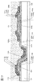
- FIG. 1A and 1B are cross-sectional views showing a configuration example of a transistor.
- 2A and 2B are cross-sectional views showing a configuration example of a transistor.
- 3A and 3B are cross-sectional views showing a configuration example of a transistor.
- 4A and 4B are cross-sectional views showing a configuration example of a transistor.
- 5A and 5B are cross-sectional views showing a configuration example of a transistor.
- 6A and 6B are cross-sectional views showing a configuration example of a transistor.
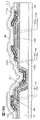
- FIG. 7 is a cross-sectional view showing a configuration example of a semiconductor device.
- FIG. 8 is a cross-sectional view showing a configuration example of the transistor.
- FIG. 9 is a cross-sectional view showing a configuration example of a semiconductor device.
- FIG. 10 is a cross-sectional view showing a configuration example of a semiconductor device.
- 11A, 11B and 11C are cross-sectional views illustrating a method for manufacturing a semiconductor device.
- 12A and 12B are cross-sectional views illustrating a method for manufacturing a semiconductor device.
- 13A and 13B are cross-sectional views illustrating a method for manufacturing a semiconductor device.
- FIG. 14 is a cross-sectional view illustrating a method for manufacturing a semiconductor device.
- FIG. 15 is a cross-sectional view illustrating a method for manufacturing a semiconductor device.
- FIG. 16 is a cross-sectional view illustrating a method for manufacturing a semiconductor device.
- FIG. 17 is a cross-sectional view illustrating a method for manufacturing a semiconductor device.
- FIG. 18 is a cross-sectional view illustrating a method for manufacturing a semiconductor device.
- 19A and 19B are cross-sectional views illustrating a method for manufacturing a semiconductor device.
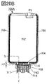
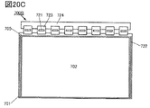
- 20A, 20B and 20C are top views of the display device.
- FIG. 21 is a cross-sectional view of the display device.
- FIG. 22 is a cross-sectional view of the display device.
- FIG. 23 is a cross-sectional view of the display device.
- FIG. 24 is a cross-sectional view of the display device.
- FIG. 25 is a cross-sectional view of the display device.
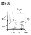
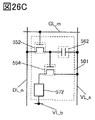
- FIG. 26A is a block diagram of the display device.
- 26B and 26C are circuit diagrams of the display device.
- 27A, 27C and 27D are circuit diagrams of the display device.
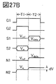
- 27B is a timing chart of the display device.
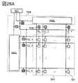
- 28A and 28B are configuration examples of the display module.
- 29A and 29B are configuration examples of electronic devices.
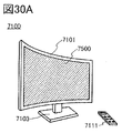
- 30A, 30B, 30C and 30D are configuration examples of electronic devices.
- 31A and 31B are STEM images according to the embodiment.
- 32A and 32B are STEM images according to the embodiment.
- 33A and 33B are STEM images according to the embodiment.
- source and drain functions of a transistor may be interchanged when transistors having different polarities are used or when the direction of current changes in circuit operation. Therefore, the terms source and drain can be used interchangeably.
- “electrically connected” includes the case of being connected via "something having some kind of electrical action”.
- the “thing having some kind of electrical action” is not particularly limited as long as it enables the exchange of electric signals between the connection targets.
- “things having some kind of electrical action” include electrodes and wirings, switching elements such as transistors, resistance elements, inductors, capacitors, and other elements having various functions.
- membrane and the term “layer” can be interchanged with each other.
- conductive layer may be interchangeable with the term “conductive layer”.
- insulating layer may be interchangeable with the term “insulating film”.
- the off current means a drain current when the transistor is in an off state (also referred to as a non-conducting state or a cutoff state).
- the off state is a state in which the voltage V gs between the gate and the source is lower than the threshold voltage V th in the n-channel transistor (higher than V th in the p-channel transistor) unless otherwise specified. To say.
- the display panel which is one aspect of the display device, has a function of displaying (outputting) an image or the like on the display surface. Therefore, the display panel is an aspect of the output device.
- an IC is mounted on a display panel board, for example, a connector such as FPC (Flexible Printed Circuit) or TCP (Tape Carrier Package) is attached, or an IC is mounted on the board by a COG (Chip On Glass) method or the like. It may be referred to as a display panel module, a display module, or simply a display panel.
- a connector such as FPC (Flexible Printed Circuit) or TCP (Tape Carrier Package) is attached, or an IC is mounted on the board by a COG (Chip On Glass) method or the like.
- COG Chip On Glass
- the touch panel which is one aspect of the display device, has a function of displaying an image or the like on the display surface, and the display surface is touched, pressed, or approached by a detected object such as a finger or a stylus. It has a function as a touch sensor for detection. Therefore, the touch panel is one aspect of the input / output device.
- the touch panel can also be referred to as, for example, a display panel with a touch sensor (or a display device) or a display panel with a touch sensor function (or a display device).
- the touch panel may be configured to have a display panel and a touch sensor panel. Alternatively, it may be configured to have a function as a touch sensor inside or on the surface of the display panel.
- a touch panel board on which a connector or an IC is mounted may be referred to as a touch panel module, a display module, or simply a touch panel.
- One aspect of the present invention is a semiconductor device having a substrate, an island-shaped first insulating layer on the substrate, and a transistor on the substrate and the first insulating layer.
- the transistor has a gate electrode, a gate insulating layer, a semiconductor layer, and a pair of conductive layers.
- One of the pair of conductive layers functions as one of the source electrode or the drain electrode, and the other of the pair of conductive layers functions as the other of the source electrode or the drain electrode.
- One of the pair of conductive layers is provided on the first insulating layer and has a region overlapping with the first insulating layer.
- the other of the pair of conductive layers has a region that does not overlap with the first insulating layer.
- the height of the other end face of the pair of conductive layers is lower than the height of one end face of the pair of conductive layers.
- an island-shaped first insulating layer and an island-shaped second insulating layer are provided on a substrate, and a transistor is provided on the substrate and the first insulating layer.
- a transistor is provided on the substrate and the first insulating layer.
- the pair of conductive layers possessed by the transistor forms a resist on the conductive film to be the pair of conductive layers, and the resist is exposed and developed using a photomask having a light-shielding portion to form a resist mask.
- a photomask having a light-shielding portion to form a resist mask.
- the thickness of the resist is thin on the first insulating layer and thicker between the first insulating layer and the second insulating layer.
- a first unexposed region that is shielded by the light-shielding portion of the photomask is formed on the first insulating layer.
- a second insulating layer is provided between the first insulating layer and the second insulating layer. Form an unexposed area.
- a first resist mask and a second resist mask can be formed in the first unexposed region and the second unexposed region, respectively.
- a pair of conductive layers can be formed by processing a conductive film using the first resist mask and the second resist mask as masks.
- one of the pair of conductive layers and the pair of conductive layers are formed.
- the distance between the layer and the other can be made smaller than the exposure limit of the exposure apparatus.
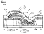
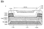
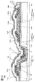
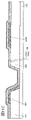
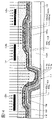
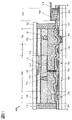
- the transistor 100 has a conductive layer 104, an insulating layer 106, a semiconductor layer 108, a conductive layer 112a, and a conductive layer 112b.
- the conductive layer 104 functions as a gate electrode.
- a part of the insulating layer 106 functions as a gate insulating layer.
- the conductive layer 112a functions as one of the source electrode and the drain electrode, and the conductive layer 112b functions as the other.
- the region of the semiconductor layer 108 that overlaps with the conductive layer 104 functions as a channel forming region.
- the transistor 100 is a so-called bottom gate type transistor having a gate electrode below the semiconductor layer 108. Further, since the source electrode and the drain electrode are provided above the semiconductor layer 108, it can be said to be a BGTC type transistor. Here, the surface of the semiconductor layer 108 opposite to the conductive layer 104 side may be referred to as a back channel side surface.
- the transistor 100 is a transistor having a so-called channel etch structure, which does not have a protective layer between the back channel side of the semiconductor layer 108 and the source electrode and the drain electrode.
- the transistor 100 is provided on the insulating layer 110.
- the insulating layer 110 has an island-like shape and is provided on the substrate 102.
- the conductive layer 104 is provided on the insulating layer 110 and is in contact with the upper surface and the side surface of the insulating layer 110.
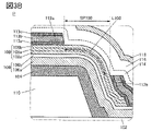
- the conductive layer 104 has a curved shape along the shape of the upper surface and the side surface of the insulating layer 110. Further, the conductive layer 104 may be further in contact with the substrate 102. One end of the conductive layer 104 may be in contact with the insulating layer 110, and the other end may be in contact with the substrate 102.
- the step between the end portion of the conductive layer 104 and the substrate 102 becomes small. Therefore, the step covering property of the layer (for example, the insulating layer 106) formed on the conductive layer 104 is improved, and it is possible to suppress the occurrence of problems such as step breakage or voids in the layer.
- the insulating layer 106 is provided on the insulating layer 110, the conductive layer 104, and the substrate 102, and is in contact with the upper surface of the insulating layer 110, the upper surface and side surfaces of the conductive layer 104, and the substrate 102.
- the insulating layer 106 may be provided on the island-shaped insulating layer 110A adjacent to the insulating layer 110 and may be in contact with the upper surface and the side surface of the insulating layer 110A.
- the semiconductor layer 108 has an island-like shape and is in contact with the upper surface of the insulating layer 106.
- the semiconductor layer 108 has a region that overlaps with the conductive layer 104 via the insulating layer 106.
- the conductive layer 112a and the conductive layer 112b are each provided on the semiconductor layer 108 and are in contact with the upper surface of the semiconductor layer 108. Further, the conductive layer 112a and the conductive layer 112b may be in contact with the side surface of the semiconductor layer 108 and the upper surface of the insulating layer 106, respectively.
- the conductive layer 112a has a region overlapping with the insulating layer 110 and is provided on the insulating layer 110.
- the conductive layer 112b is provided in the groove 111 between the insulating layer 110 and the island-shaped insulating layer 110A adjacent to the insulating layer 110.
- the conductive layer 112b has a region that does not overlap with the insulating layer 110.
- the conductive layer 112b has a U-shaped shape in a cross-sectional view. Therefore, the height of the side surface of the conductive layer 112b may be higher than the height of the upper surface of the conductive layer 112b.
- the height of the upper surface of the conductive layer 112b located in the groove 111 is lower than the height of the upper surface of the conductive layer 112a located on the insulating layer 110.
- the height of the side surface of the conductive layer 112b is lower than the height of the side surface of the conductive layer 112a.
- the height of the end face of the conductive layer 112b is lower than the height of the end face of the conductive layer 112a.
- the end surface of the layer includes the upper surface and the side surface when the surface in contact with the surface to be formed of the layer is the lower surface.
- the height from the substrate to the highest portion of the upper surface of the layer is used.
- the height from the substrate to the highest part of the sides of the layer is used.
- the height from the substrate to the highest portion of the end faces (top and side surfaces) of the layer is used.
- FIG. 1A shows an example in which the height of one end of the conductive layer 112b and the height of the other end are the same or substantially the same, but one aspect of the present invention is not limited to this.
- the height of one end of the conductive layer 112b and the height of the other end may be different.
- the same material for the conductive layer 112a and the conductive layer 112b it is preferable to use the same material for the conductive layer 112a and the conductive layer 112b.
- the resistivity of the conductive layer 112a and the conductive layer 112b can be the same or substantially the same.
- the end of the insulating layer 110 is preferably tapered.
- the taper angle ⁇ at the end of the insulating layer 110 is preferably less than 90 degrees.
- the taper angle ⁇ at the end of the insulating layer 110 is preferably 45 degrees or more and less than 90 degrees, more preferably 50 degrees or more and 85 degrees or less, further preferably 55 degrees or more and 85 degrees or less, and further preferably 60 degrees or more and 85 degrees.
- the following is preferable, more preferably 60 degrees or more and 80 degrees or less, further preferably 65 degrees or more and 80 degrees or less, and further preferably 70 degrees or more and 80 degrees or less.
- the step covering property of the layer (for example, the conductive layer 104) formed on the insulating layer 110 is improved, and the layer has problems such as step breakage or voids. It can be suppressed from occurring.
- the distance between the conductive layer 112a and the conductive layer 112b can be made smaller than the exposure limit of the exposure apparatus.
- the end portion of the insulating layer 110A has a tapered shape.
- the taper angle of the insulating layer 110A the description of the insulating layer 110 can be referred to, and detailed description thereof will be omitted.
- the taper angle ⁇ of the insulating layer 110 and the taper angle of the insulating layer 110A may be the same or different.
- the taper angle refers to the angle formed by the end surface of the layer and the formed surface of the layer.
- FIG. 1A shows an example in which the insulating layer 110 and the insulating layer 110A have the same thickness.
- the insulating layer 110 and the insulating layer 110A can be formed in the same process.
- the insulating layer 110 and the insulating layer 110A may be formed in different steps. Further, the thicknesses of the insulating layer 110 and the insulating layer 110A may be different.
- FIG. 1A shows an example in which the insulating layer 110 and the insulating layer 110A are provided in contact with the substrate 102, but one aspect of the present invention is not limited to this.
- Another insulating layer may be provided on the substrate 102, and the insulating layer 110 and the insulating layer 110A may be provided on the insulating layer.
- the insulating layer may be provided between the conductive layer 104 and the substrate 102, and between the insulating layer 106 and the substrate 102.
- Another insulating layer may be provided on the substrate 102, the insulating layer 110, and the insulating layer 110A, and the conductive layer 104 may be provided on the insulating layer.
- the insulating layer may be provided between the insulating layer 106 and the substrate 102, between the insulating layer 106 and the insulating layer 110, and between the insulating layer 106 and the insulating layer 110A.
- FIG. 1B An enlarged view of the region P surrounded by the alternate long and short dash line in FIG. 1A is shown in FIG. 1B.
- the channel length L100 can be the length of the semiconductor layer 108 between the conductive layer 112a and the conductive layer 112b. Further, the channel length L100 can be said to be the length of the semiconductor layer 108 in the region between the conductive layer 112a and the conductive layer 112b, which is in contact with neither the conductive layer 112a nor the conductive layer 112b.
- the semiconductor layer 108 has a curved region between the conductive layer 112a and the conductive layer 112b. It can be said that the transistor 100 has a channel forming region having a curved shape. Further, the interval SP100 and the channel length L100 are different values, and the channel length L100 is a value larger than the interval SP100.
- the channel length L100 can be set to a value smaller than the exposure limit of the exposure apparatus.
- the channel length L100 is preferably 0.2 ⁇ m or more and less than 1.5 ⁇ m, more preferably 0.3 ⁇ m or more and 1.3 ⁇ m or less, further preferably 0.4 ⁇ m or less and 1.2 ⁇ m, and further preferably 0.5 ⁇ m or less 1. .1 ⁇ m is preferable, and more preferably 0.6 ⁇ m or less and 1.0 ⁇ m.
- the transistor 100 can have a channel length L100 smaller than the exposure limit of the exposure apparatus by providing the conductive layer 112a on the insulating layer 110 and providing the conductive layer 112b in the groove 111. For example, when the exposure limit of the exposure apparatus is 1.5 ⁇ m, the channel length L100 can be set to less than 1.5 ⁇ m.
- the on-current of the transistor 100 can be increased.
- the transistor 100 it is possible to manufacture a circuit capable of high-speed operation.
- An insulating layer 114, an insulating layer 116, and an insulating layer 118 are provided so as to cover the conductive layer 112a, the conductive layer 112b, and the semiconductor layer 108.
- the insulating layer 114, the insulating layer 116, and the insulating layer 118 each function as a protective layer for the transistor 100.
- the conductive layer 104 is preferable because the electric resistance can be lowered by using a conductive film containing a metal or an alloy. In particular, it is preferable to use a conductive material containing copper as the conductive layer 104. An oxide film may be used for the conductive layer 104.
- an oxide film for the insulating layer 106 It is preferable to use an oxide film for the insulating layer 106. In particular, it is preferable to use an oxide film for the portion in contact with the semiconductor layer 108.
- the insulating layer 106 preferably has a high dielectric strength. Due to the high dielectric strength of the insulating layer 106, a highly reliable transistor can be obtained.
- the insulating layer 106 has a small absolute value of stress. Since the absolute value of the stress of the insulating layer 106 is small, it is possible to suppress the occurrence of problems during the process due to stress such as warping of the substrate.
- the insulating layer 106 preferably functions as a barrier membrane that prevents impurities such as water, hydrogen, and sodium from diffusing from the substrate 102 side to the transistor 100. Further, it is preferable that the insulating layer 106 functions as a barrier film for suppressing the diffusion of the components of the conductive layer 104 to the transistor 100. Since the insulating layer 106 functions as a barrier membrane that suppresses the diffusion of impurities and the like, it is possible to obtain a transistor that exhibits good electrical characteristics and has high reliability.
- the insulating layer 106 emits less impurities such as water and hydrogen from itself. Since the emission of impurities from the insulating layer 106 is small, it is possible to suppress the diffusion of impurities to the transistor 100 side, and it is possible to obtain a transistor having good electrical characteristics and high reliability.
- the insulating layer 106 functions as a barrier membrane that suppresses the diffusion of oxygen. Since the insulating layer 106 has a function of suppressing the diffusion of oxygen, it is possible to suppress the diffusion of oxygen from above the insulating layer 106 to the conductive layer 104 and to suppress the oxidation of the conductive layer 104. As a result, a transistor exhibiting good electrical characteristics and having high reliability can be obtained.
- the insulating layer 106 may have a laminated structure.
- FIG. 1A shows a configuration in which the insulating layer 106 has a two-layer structure of the insulating layer 106a and the insulating layer 106b on the insulating layer 106a.
- a nitride film can be used for the insulating layer 106a located on the substrate 102 side, and an oxide film can be used for the insulating layer 106b in contact with the semiconductor layer 108.
- the insulating layer 106a preferably has a high dielectric strength. Due to the high dielectric strength of the insulating layer 106, a highly reliable transistor can be obtained.
- the insulating layer 106a preferably has a small absolute value of stress. Since the absolute value of the stress of the insulating layer 106 is small, it is possible to suppress the occurrence of problems during the process due to stress such as warping of the substrate.
- the insulating layer 106a preferably functions as a barrier membrane that prevents impurities such as water, hydrogen, and sodium from diffusing from the substrate 102 side to the transistor 100. Further, it is preferable that the insulating layer 106a functions as a barrier membrane for suppressing the diffusion of the components of the conductive layer 104 to the transistor 100. Since the insulating layer 106a has a function of suppressing the diffusion of impurities and the like, it is possible to obtain a transistor exhibiting good electrical characteristics and having high reliability.
- the insulating layer 106a emits less impurities such as water and hydrogen from itself. Since the emission of impurities from the insulating layer 106a is small, it is possible to suppress the diffusion of impurities to the transistor 100 side, and it is possible to obtain a transistor having good electrical characteristics and high reliability.
- the insulating layer 106a functions as a barrier membrane that suppresses the diffusion of oxygen. Since the insulating layer 106a has a function of suppressing the diffusion of oxygen, it is possible to suppress the diffusion of oxygen from above the insulating layer 106a to the conductive layer 104 and to suppress the oxidation of the conductive layer 104. As a result, a transistor exhibiting good electrical characteristics and having high reliability can be obtained.
- Examples of the insulating layer 106a include oxide films such as aluminum oxide, aluminum nitride, hafnium oxide, hafnium oxide, gallium oxide, gallium nitride, yttrium oxide, and yttrium oxide, silicon nitride, silicon nitride, and aluminum nitride.
- a nitride film such as aluminum nitride can be used.
- Silicon nitride can be particularly preferably used as the insulating layer 106a.
- the insulating layer 106b has a region in contact with the channel forming region of the semiconductor layer 108.
- the insulating layer 106b preferably has a low defect density. Further, it is preferable that the insulating layer 106b emits less impurities having hydrogen such as water and hydrogen from itself.
- an oxide film such as silicon oxide or silicon nitride can be preferably used.
- the insulating layer 106 in a laminated structure, it is possible to obtain a transistor exhibiting good electrical characteristics and having high reliability.
- a nitride film may be formed as the insulating layer 106a, and then oxygen may be added to the upper portion of the insulating layer 106a to form a region containing oxygen, and the region containing oxygen may be used as the insulating layer 106b.
- the treatment for adding oxygen includes, for example, heat treatment or plasma treatment in an atmosphere containing oxygen, and ion doping treatment.
- the oxidative nitride refers to a substance having a higher oxygen content than nitrogen as its composition, and the oxidative nitride is contained in the oxide.
- the nitride oxide refers to a substance having a higher nitrogen content than oxygen as its composition, and the nitride oxide is contained in the nitride.
- FIG. 1A shows a two-layer structure of the insulating layer 106a and the insulating layer 106b as the insulating layer 106, but one aspect of the present invention is not limited to this.
- the insulating layer 106 may have a single-layer structure or a laminated structure of three or more layers. Further, each of the insulating layer 106a and the insulating layer 106b may have a laminated structure of two or more layers.
- the semiconductor layer 108 is configured to contain a metal oxide exhibiting semiconductor characteristics (hereinafter, also referred to as an oxide semiconductor).
- Oxide semiconductors are divided into single crystal oxide semiconductors and other non-single crystal oxide semiconductors.
- Non-single crystal oxide semiconductors include, for example, CAAC-OS, polycrystalline oxide semiconductors, nc-OS, pseudoamorphous oxide semiconductors (a-like OS: amorphous-like oxide semiconductor), and amorphous oxides. There are semiconductors and so on.
- the semiconductor layer 108 preferably contains at least indium and oxygen. Since the semiconductor layer 108 contains an oxide of indium, carrier mobility can be increased, and for example, a transistor capable of passing a larger current than amorphous silicon can be realized.
- the semiconductor layer 108 preferably contains at least a metal oxide containing indium and oxygen. Further, the semiconductor layer 108 may contain zinc in addition to these. Further, the semiconductor layer 108 may contain gallium.
- indium oxide indium zinc oxide (In-Zn oxide), indium gallium zinc oxide (also referred to as In-Ga-Zn oxide, IGZO) and the like can be typically used. .. Further, indium tin oxide (In—Sn oxide), indium tin oxide containing silicon, or the like can also be used.
- the semiconductor layer 108 includes indium and element M (element M is gallium, aluminum, silicon, boron, ittrium, tin, copper, vanadium, beryllium, titanium, iron, nickel, germanium, zirconium, molybdenum, lanthanum, cerium). , One or more selected from neodyllium, hafnium, tantalum, tungsten, or magnesium) and zinc.
- element M is preferably one or more selected from aluminum, gallium, yttrium, or tin.
- the semiconductor layer 108 it is preferable to use an oxide containing indium, gallium, and zinc as the semiconductor layer 108.
- the atomic number ratio of In is equal to or higher than the atomic number ratio of Ga.
- the vicinity of can be used.
- the semiconductor layer 108a and the semiconductor layer 108b may have the same composition or substantially the same composition.
- the semiconductor layer 108a and the semiconductor layer 108b can be formed by using the same sputtering target, so that the manufacturing cost can be reduced.
- a metal oxide film having crystallinity for the semiconductor layer 108.
- a metal oxide film having a CAAC (c-axis aligned crystal) structure, a polycrystal structure, a microcrystal (nc: nano-crystal) structure, which will be described later, can be used.
- CAAC c-axis aligned crystal
- nc nano-crystal
- the thickness of the semiconductor layer 108 is preferably 10 nm or more and 100 nm or less, more preferably 15 nm or more and 70 nm or less, further preferably 20 nm or more and 50 nm or less, and further preferably 25 nm or more and 40 nm or less.
- the substrate temperature at the time of forming the semiconductor layer 108 is preferably room temperature (25 ° C.) or higher and 200 ° C. or lower, and more preferably room temperature or higher and 130 ° C. or lower. By setting the substrate temperature within the above range, bending or distortion of the substrate can be suppressed when a glass substrate having a large area is used.
- the semiconductor layer 108 contains an oxide semiconductor
- hydrogen contained in the oxide semiconductor reacts with oxygen bonded to a metal atom to become water, and oxygen deficiency (VO: Oxygen Vacuumy ) is formed in the oxide semiconductor.
- VO oxygen deficiency
- a defect containing hydrogen in an oxygen deficiency (hereinafter referred to as VOH) may function as a donor and generate electrons as carriers.
- a part of hydrogen may be combined with oxygen that is bonded to a metal atom to generate an electron as a carrier. Therefore, a transistor using an oxide semiconductor containing a large amount of hydrogen tends to have normally-on characteristics. Further, since hydrogen in an oxide semiconductor is easily moved by stress such as heat and electric field, if a large amount of hydrogen is contained in the oxide semiconductor, the reliability of the transistor may be deteriorated.
- VOH can function as a donor of oxide semiconductors.
- the carrier concentration may be used for evaluation instead of the donor concentration. Therefore, in the present specification and the like, as a parameter of the oxide semiconductor, a carrier concentration assuming a state in which an electric field is not applied may be used instead of the donor concentration. That is, the "carrier concentration" described in the present specification and the like may be paraphrased as a "donor concentration".
- the VOH in the semiconductor layer 108 when an oxide semiconductor is used for the semiconductor layer 108, it is preferable to reduce the VOH in the semiconductor layer 108 as much as possible to achieve high-purity intrinsicity or substantially high-purity intrinsicity.
- impurities such as water and hydrogen in the oxide semiconductor must be removed (may be described as dehydration or dehydrogenation treatment). It is important to supply oxygen to the oxide semiconductor to compensate for the oxygen deficiency (sometimes referred to as oxygenation treatment).
- oxygenation treatment oxygenation treatment
- the carrier concentration of the oxide semiconductor in the region functioning as a channel forming region is preferably 1 ⁇ 10 18 cm -3 or less, and less than 1 ⁇ 10 17 cm -3 . It is more preferably less than 1 ⁇ 10 16 cm -3 , even more preferably less than 1 ⁇ 10 13 cm -3 , still more preferably less than 1 ⁇ 10 12 cm -3 . ..
- the lower limit of the carrier concentration of the oxide semiconductor in the region that functions as the channel forming region is not particularly limited, but may be, for example, 1 ⁇ 10 -9 cm -3 .
- the insulating layer 114 and the insulating layer 116 have a function as a protective film for the transistor 100. Further, the insulating layer 114 and the insulating layer 116 have a function of supplying oxygen to the semiconductor layer 108.
- VO and VOH in the semiconductor layer 108 can be reduced, and the reliability is high.
- a transistor can be realized.
- Other processes for supplying oxygen to the semiconductor layer 108 include heat treatment in an atmosphere containing oxygen, plasma treatment in an atmosphere containing oxygen, and the like.
- the conductive layer 112a and the conductive layer 112b are preferable because the electric resistance can be lowered by using a conductive film containing a metal or an alloy.
- a conductive material containing copper for the conductive layer 112a and the conductive layer 112b.
- An oxide film may be used for the conductive layer 112a and the conductive layer 112b.
- the insulating layer 114 in contact with the semiconductor layer 108 preferably emits less nitrogen oxides (NO x , x is greater than 0 and 2 or less).
- Nitrogen oxides include, for example, NO 2 or NO. Further, it is preferable that the insulating layer 114 releases a large amount of ammonia.
- Nitrogen oxide forms a level on the insulating layer 114 and the like.
- the level is located within the energy gap of the semiconductor layer 108. Therefore, when nitrogen oxides diffuse to the interface between the insulating layer 114 and the semiconductor layer 108, the level may trap electrons on the insulating layer 114 side. As a result, the trapped electrons stay in the vicinity of the interface between the insulating layer 114 and the semiconductor layer 108, so that the threshold voltage of the transistor fluctuates in the positive direction.
- Nitrogen oxide reacts with ammonia and oxygen when heat is applied. Since the nitrogen oxides contained in the insulating layer 114 react with ammonia contained in the insulating layer 114 and the insulating layer 116 when heat is applied, the nitrogen oxides contained in the insulating layer 114 are reduced. Therefore, it is difficult for electrons to be trapped at the interface between the insulating layer 114 and the semiconductor layer 108.
- the insulating layer 114 preferably forms an oxide film such as a silicon oxide film or a silicon nitride nitride film using a plasma chemical vapor deposition apparatus (PECVD apparatus, or simply plasma CVD apparatus).
- PECVD apparatus plasma chemical vapor deposition apparatus
- a mixed gas containing silicon-containing sedimentary gas, oxidizing gas and ammonia gas as the raw material gas.
- the sedimentary gas having silicon for example, any one or more of silane, disilane, trisilane, and fluorinated silane can be used.
- a gas containing oxygen can be preferably used.
- oxygen O 2
- ozone O 3
- nitrous oxide N 2 O
- NO nitric oxide
- NO 2 nitrogen dioxide
- the flow rate of the oxidizing gas is preferably more than 20 times and preferably 200 times or less, more preferably 30 times or more and 150 times or less, and further preferably 40 times or more and 100 times or less with respect to the flow rate of the sedimentary gas. Further, it is preferably 40 times or more and 80 times or less.
- the flow rate of ammonia gas is preferably equal to or less than the flow rate of oxidizing gas.
- the flow rate of ammonia gas is preferably 0.01 times or more and 1 times or less, more preferably 0.02 times or more and 0.9 times or less, and further 0.03 times or more and 0.8 times or less. It is preferable, more preferably 0.04 times or more and 0.6 times or less, and further preferably 0.05 times or more and 0.5 times or less.
- the insulating layer 114 having few defects can be formed even when the pressure in the processing chamber is relatively high.
- the preferable flow rate of ammonia gas with respect to the flow rate of the oxidizing gas may differ depending on the conditions at the time of forming the insulating layer 114, for example, pressure or power.
- the pressure in the treatment chamber at the time of forming the insulating layer 114 is preferably 200 Pa or less, more preferably 150 Pa or less, further preferably 120 Pa or less, and further preferably 100 Pa or less. By setting the pressure within the above-mentioned range, it is possible to form the insulating layer 114 having a small amount of nitrogen oxides and a small amount of defects.
- the insulating layer that releases a large amount of ammonia and a small amount of nitrogen oxides is a film that releases more ammonia than the amount of nitrogen oxides released in the thermal desorption gas analysis method (TDS: Thermal Desorption Gascopy).
- TDS Thermal Desorption Gascopy
- the amount of ammonia released is 1 ⁇ 10 18 / cm 3 or more and 5 ⁇ 10 19 / cm 3 or less.
- the amount of ammonia released is such that the surface temperature of the film is in the range of 50 ° C. or higher and 650 ° C. or lower, preferably 50 ° C. or higher and 550 ° C. or lower.
- the insulating layer 114 is a film formed under conditions that cause less damage to the semiconductor layer 108.
- it can be formed under a condition that the film forming speed (also referred to as a film forming rate) is sufficiently slow.
- the damage given to the semiconductor layer 108 can be extremely reduced by forming the insulating layer 114 under low power conditions.
- the insulating layer 116 has an insulating film capable of releasing oxygen.
- forming the insulating layer 116 in an oxygen atmosphere heat-treating the formed insulating layer 116 in an oxygen atmosphere, or performing a second plasma treatment, or performing an oxide film on the insulating layer 116 in an oxygen atmosphere. It is also possible to supply oxygen into the insulating layer 116 by forming the insulating layer 116.
- the insulating layer 116 has a region in which the amount of oxygen molecules released in TDS is 1.0 ⁇ 10 19 molecules / cm 3 or more, preferably 3.0 ⁇ 10 20 molecules / cm 3 or more.
- the amount of oxygen released is the total amount in the range where the temperature of the heat treatment in TDS is 50 ° C. or higher and 650 ° C. or lower, or 50 ° C. or higher and 550 ° C. or lower.
- Examples of the insulating layer 114 and the insulating layer 116 include a silicon oxide film, a silicon nitride film, a silicon nitride film, an aluminum oxide film, a hafnium oxide film, an yttrium oxide film, a zirconium oxide film, a gallium oxide film, a tantalum oxide film, and oxidation.
- An insulating layer containing one or more magnesium film, lanthanum oxide film, cerium oxide film and neodymium oxide film can be used.
- the insulating film 114 and the insulating layer 116 can use an insulating film made of the same material, the interface between the insulating layer 114 and the insulating layer 116 may not be clearly confirmed. Therefore, in the present embodiment, the boundary (interface) between the insulating layer 114 and the insulating layer 116 may not be clearly confirmed. Therefore, in the drawings illustrating one embodiment of the present invention, these boundaries are shown by broken lines. Although the two-layer structure of the insulating layer 114 and the insulating layer 116 has been described in the present embodiment, one aspect of the present invention is not limited to this. For example, a single-layer structure of the insulating layer 114 or a laminated structure of three or more layers may be used.
- the insulating layer 114 After forming the insulating layer 114, it is preferable to continuously form the insulating layer 116 without exposing the surface of the insulating layer 114 to the atmosphere. By forming the insulating layer 116 continuously with the formation of the insulating layer 114, it is possible to suppress the adhesion of impurities to the interface between the insulating layer 114 and the insulating layer 116.
- the insulating layer 118 has a function as a protective film for the transistor 100.
- the insulating layer 118 suppresses impurities such as water and hydrogen from diffusing from the outside of the transistor 100 to the transistor 100. That is, the reliability and moisture resistance of the transistor 100 can be improved, and the semiconductor device with improved reliability can be obtained.
- the insulating layer 118 preferably functions as a barrier membrane that prevents impurities such as water and hydrogen from diffusing from the outside of the transistor 100 to the transistor 100. Further, it is preferable that the insulating layer 118 emits less impurities having hydrogen such as water and hydrogen from itself. Further, the insulating layer 118 preferably functions as a barrier membrane that suppresses the diffusion of oxygen. Examples of the insulating layer 118 include oxide films such as aluminum oxide, aluminum nitride, hafnium oxide, hafnium oxide, gallium oxide, gallium oxide, yttrium oxide, and yttrium oxide, silicon nitride, silicon nitride, and aluminum nitride. , A nitride film such as aluminum nitride can be used. Silicon nitride can be particularly preferably used as the insulating layer 118.
- the oxygen contained in the insulating layer 114 and the insulating layer 116 may be desorbed to the outside.
- the amount of oxygen contained in the insulating layer 114 and the insulating layer 116 may decrease, and the amount of oxygen supplied to the semiconductor layer 108 may decrease. .. Therefore, at least the temperature at which the insulating layer 118 starts to be formed is preferably a temperature at which the oxygen contained in the insulating layer 114 and the insulating layer 116 does not desorb outward.
- the insulating layer 118 has a function of suppressing the diffusion of oxygen, and further, by forming the insulating layer 118 at a temperature at which the oxygen contained in the insulating layer 114 and the insulating layer 116 does not desorb to the outside, oxygen is formed in the semiconductor layer 108. Can be supplied, and oxygen deficiency in the semiconductor layer 108 can be efficiently compensated.
- the insulating layer 118 having a function of suppressing the diffusion of impurities such as water and hydrogen and a function of suppressing the diffusion of oxygen is preferably a dense film. For example, by raising the substrate temperature at the time of forming the insulating layer 118, a dense film can be obtained.
- the substrate temperature at the time of forming the insulating layer 118 is preferably 180 ° C. or higher and 400 ° C. or lower, more preferably 200 ° C. or higher and 380 ° C. or lower, further preferably 220 ° C. or higher and 360 ° C. or lower, and further preferably 240 ° C. or higher and 350 ° C. or lower. Is preferable.
- the substrate temperature By setting the substrate temperature within the above range, it is possible to suppress the oxygen contained in the insulating layer 114 and the insulating layer 116 from desorbing outward, and the insulating layer 118 can be made into a dense film.
- FIG. 1A shows an example in which the conductive layer 112a and the conductive layer 112b have a laminated structure in which the conductive layer 113a, the conductive layer 113b, and the conductive layer 113c are laminated in order from the surface to be formed, respectively.
- the conductive layer 113a and the conductive layer 113c can independently use a conductive material different from that of the conductive layer 113b.
- sandwiching the conductive layer 113b between the conductive layer 113a and the conductive layer 113c it is possible to prevent the surface of the conductive layer 113b from being oxidized and the components of the conductive layer 113b from diffusing into the surrounding layers.
- the conductive layer 112a and the conductive layer 112b can have extremely low resistance.
- the conductive layer 113c located at the uppermost portion contains a material that is less likely to bond with oxygen than a conductive film containing copper, aluminum, or the like, or a material whose conductivity is not easily impaired even when oxidized. Is preferable. Further, for the conductive layer 113a in contact with the semiconductor layer 108, it is preferable to use a material in which oxygen in the semiconductor layer 108 does not easily diffuse.
- the conductive layer 113c located at the uppermost portion and the conductive layer 113a in contact with the semiconductor layer use, for example, a conductive material containing one or more of titanium, tungsten, molybdenum, chromium, tantalum, zinc, indium, platinum, or ruthenium. be able to.
- a conductive material containing one or more of titanium, tungsten, molybdenum, chromium, tantalum, zinc, indium, platinum, or ruthenium be able to.
- the same conductive material can be used for the conductive layer 113a and the conductive layer 113c.
- different conductive materials may be used for the conductive layer 113a and the conductive layer 113c.
- the conductive layer 113b preferably contains one or more of copper, silver, gold, or aluminum. In particular, it is preferable that the conductive layer 113b contains one or more of copper or aluminum.
- the conductive layer 113b it is preferable to use a conductive material having a lower resistance than the conductive layer 113a and the conductive layer 113c. As a result, the conductive layer 112a and the conductive layer 112b can have extremely low resistance.
- the insulating layer 114 is provided in contact with the end portion of the conductive layer 113b. According to one aspect of the present invention, even when an insulating layer 114 containing an oxide film is formed on the conductive layer 113b using a conductive material which is easily oxidized, before the insulating layer 114 is formed.
- plasma treatment hereinafter, also referred to as first plasma treatment
- the structure of the conductive layer 112a and the conductive layer 112b is not limited to the three-layer structure, and may be a two-layer structure including a conductive layer containing copper, silver, gold, or aluminum, or a four-layer structure.
- the conductive layer 112a and the conductive layer 112b may have a two-layer structure in which the conductive layer 113a and the conductive layer 113b are laminated, or a two-layer structure in which the conductive layer 113b and the conductive layer 113c are laminated.
- the surface of the semiconductor layer 108 may be damaged. Since VO is formed on the damaged semiconductor layer 108 and hydrogen in the semiconductor layer 108 may enter VO and form VO H , the damaged layer is removed. May be good. By removing the damaged layer, a transistor exhibiting good electrical characteristics and having high reliability can be obtained. In this case, the film thickness of the region of the semiconductor layer 108 that does not overlap with either the conductive layer 112a or the conductive layer 112b is thinner than the film thickness of the region that overlaps with either the conductive layer 112a or the conductive layer 112b.
- FIG. 1A and 1B show examples in which the ends of the conductive layer 113a, the conductive layer 113b, and the conductive layer 113c all match or substantially match, but one aspect of the present invention is not limited to this. Any of the ends of the conductive layer 113a, the conductive layer 113b, and the conductive layer 113c may not match or may not substantially match.
- the ends of the conductive layer 113b and the conductive layer 113c may be located inside the ends of the conductive layer 113a.
- the step covering property of the layer (for example, the insulating layer 114) formed on the conductive layer 113a, the conductive layer 113b, the conductive layer 113c, and the semiconductor layer 108 is improved, and the step is cut into the layers.
- the ends of the conductive layer 113b and the conductive layer 113c do not match or do not roughly match.
- the step coating of the layer for example, the insulating layer 118
- the properties may deteriorate, and problems such as step breaks or voids may occur in the layer. Therefore, it is preferable that the end portion of the conductive layer 113c is located inside the end portion of the conductive layer 113b.
- the above-mentioned conductive material that can be used for the conductive layer 113a and the conductive layer 113b can be appropriately used.
- an insulating material containing an oxide for the insulating layer 106 and the insulating layer 114 in contact with the semiconductor layer 108.
- an insulating material containing an oxide is used for the layer in contact with the semiconductor layer 108.
- a nitride film such as silicon nitride or aluminum nitride may be used for the insulating layer 106.
- a treatment of adding oxygen includes, for example, heat treatment or plasma treatment in an atmosphere containing oxygen, and ion doping treatment.
- the insulating layer 116 functions as a protective layer that protects the transistor 100.
- an inorganic insulating material such as silicon nitride, silicon nitride oxide, silicon oxide, silicon oxide, aluminum oxide, or aluminum nitride can be used.
- silicon nitride or aluminum oxide that does not easily diffuse oxygen as the insulating layer 116, the semiconductor layer 108 or the insulating layer 114 can be removed from the semiconductor layer 108 or the insulating layer 114 to the outside via the insulating layer 116 due to heat applied during the manufacturing process. It is preferable because it can prevent oxygen from being desorbed.
- An organic insulating material that functions as a flattening film may be used as the insulating layer 116.
- a film containing an inorganic insulating material and a laminated film containing an organic insulating material may be used as the insulating layer 116.
- the semiconductor layer 108 may be located in or near a portion in contact with the conductive layer 112a and the conductive layer 112b, and a pair of low resistance regions functioning as a source region and a drain region may be formed.
- This region is a part of the semiconductor layer 108 and has a lower resistance than the channel formation region.
- the low resistance region can be rephrased as a region having a high carrier concentration, a region having an n-type, or the like.
- a region sandwiched between a pair of low resistance regions and overlapping with the conductive layer 104 functions as a channel forming region.
- FIG. 2A shows a schematic cross-sectional view of the transistor 100A applicable to the semiconductor device according to the present invention in the channel length direction.
- An enlarged view of the region P surrounded by the alternate long and short dash line in FIG. 2A is shown in FIG. 2B.
- the transistor 100A is mainly different from the above-mentioned transistor 100 in that the semiconductor layer 108 has a laminated structure of the semiconductor layer 108a and the semiconductor layer 108b on the semiconductor layer 108a.
- the semiconductor layer 108a and the semiconductor layer 108b each contain a metal oxide.
- the boundary (interface) between the semiconductor layer 108a and the semiconductor layer 108b cannot be clearly confirmed. Therefore, in the drawings illustrating one embodiment of the present invention, these boundaries are shown by broken lines.
- the semiconductor layer 108b located on the back channel side has a region having higher crystallinity than the semiconductor layer 108a located on the conductive layer 104 side. Since the semiconductor layer 108b has a highly crystalline region, it is possible to prevent a part of the semiconductor layer 108 from being etched and disappearing when the conductive layer 112a and the conductive layer 112b are formed. Further, it is possible to prevent the semiconductor layer 108 from being damaged when the surface of the semiconductor layer 108 is cleaned.
- the semiconductor layer 108a and the semiconductor layer 108b can be made separately, for example, by different formation conditions.
- the flow rates of oxygen gas in the film-forming gas can be made different between the semiconductor layer 108a and the semiconductor layer 108b.
- the ratio of the oxygen gas flow rate (also referred to as the oxygen flow rate ratio or the oxygen partial pressure) to the total gas flow rate is preferably 0% or more and less than 50%, and further 5% or more and 30% or less. Is preferable, and more preferably 5% or more and 20% or less.
- the oxygen flow rate ratio at the time of forming the semiconductor layer 108b is preferably higher than the oxygen flow rate ratio at the time of forming the semiconductor layer 108a. Further, as a condition for forming the semiconductor layer 108b, the oxygen flow rate ratio is preferably 50% or more and 100% or less, more preferably 60% or more and 100% or less, further preferably 70% or more and 100% or less, and further preferably 80% or more. 100% or less is preferable. By setting the oxygen flow rate ratio as described above, the crystallinity of the semiconductor layer 108b can be increased.
- the semiconductor layer 108 has a laminated structure, it is preferable to continuously form the semiconductor layer 108 in the same processing chamber using the same sputtering target because the interface can be improved.
- the formation conditions of each metal oxide film conditions such as pressure, temperature, and electric power at the time of formation may be different, but by making the conditions other than the oxygen flow rate ratio the same, the time required for the formation step can be reduced. It is preferable because it can be shortened.
- a laminated structure of metal oxide films having different compositions may be used as the semiconductor layer 108. When laminating metal oxide films having different compositions, it is preferable to form them continuously without exposing them to the atmosphere.
- productivity can be improved by setting the substrate temperature at the time of formation of the semiconductor layer 108a and the semiconductor layer 108b to the same temperature.
- the substrate temperature at the time of forming the semiconductor layer 108b is higher than the substrate temperature at the time of forming the semiconductor layer 108a.
- the semiconductor layer 108b preferably has a region having higher crystallinity than the semiconductor layer 108a.
- a CAC-OS Cloud-Aligned Composite oxide semiconductor
- CAAC-OS c-axis-aligned crystalline oxide semiconductor
- the crystallinity of the semiconductor layer 108a and the semiconductor layer 108b can be analyzed by, for example, X-ray diffraction (XRD: X-Ray Diffraction), transmission electron microscope (TEM: Transmission Electron Microscope), electron diffraction (Electron Diffraction), or the like.
- the thickness of the semiconductor layer 108a is preferably 1 nm or more and 50 nm or less, more preferably 5 nm or more and 30 nm or less, and further preferably 5 nm or more and 20 nm or less.
- the thickness of the semiconductor layer 108b is preferably 1 nm or more and 50 nm or less, more preferably 5 nm or more and 30 nm or less, and further preferably 5 nm or more and 20 nm or less.
- the semiconductor layer 108a and the semiconductor layer 108b layers having different compositions, layers having different crystallinity, or layers having different impurity concentrations may be used. Further, the semiconductor layer 108 may have a laminated structure of three or more layers.
- FIG. 3A shows a schematic cross-sectional view of the transistor 100B applicable to the semiconductor device according to the present invention in the channel length direction.
- An enlarged view of the region P surrounded by the alternate long and short dash line in FIG. 3A is shown in FIG. 3B.
- the transistor 100B is mainly different from the above-mentioned transistor 100 in that the semiconductor layer 108 has a laminated structure of the semiconductor layer 108c, the semiconductor layer 108a on the semiconductor layer 108c, and the semiconductor layer 108b on the semiconductor layer 108a. ..
- the semiconductor layer 108a and the semiconductor layer 108b since the above description can be referred to, detailed description thereof will be omitted.
- the semiconductor layer 108a, the semiconductor layer 108b, and the semiconductor layer 108c each contain a metal oxide.
- the boundary (interface) between the semiconductor layer 108a and the semiconductor layer 108b the boundary (interface) between the semiconductor layer 108c and the semiconductor layer 108a may not be clearly confirmed. Therefore, in the drawings illustrating one embodiment of the present invention, these boundaries are shown by broken lines.
- the semiconductor layer 108c located on the insulating layer 106 side preferably has a region having higher crystallinity than the semiconductor layer 108a.
- the semiconductor layer 108a, the semiconductor layer 108b, and the semiconductor layer 108c can be made separately, for example, by different formation conditions.
- the flow rates of oxygen gas in the film-forming gas can be made different in the semiconductor layer 108a, the semiconductor layer 108b, and the semiconductor layer 108c.
- the oxygen flow rate ratio at the time of forming the semiconductor layer 108c is preferably higher than the oxygen flow rate ratio at the time of forming the semiconductor layer 108a. Further, as a condition for forming the semiconductor layer 108c, the oxygen flow rate ratio is preferably 50% or more and 100% or less, more preferably 60% or more and 100% or less, further preferably 70% or more and 100% or less, and further preferably 80% or more. 100% or less is preferable.
- oxygen flow rate ratio as described above, oxygen can be suitably supplied to the insulating layer 106 when the film to be the semiconductor layer 108c is formed.
- oxygen deficiency VOH and VOH in the semiconductor layer 108 can be reduced.
- the crystallinity of the semiconductor layer 108c can be increased.
- the semiconductor layer 108c preferably has a region having higher crystallinity than the semiconductor layer 108a. Further, the semiconductor layer 108b preferably has a region having higher crystallinity than the semiconductor layer 108a.
- the crystallinity of the semiconductor layer 108c can be analyzed by the same method as that of the semiconductor layer 108a and the semiconductor layer 108b.
- the thickness of the semiconductor layer 108c is preferably 1 nm or more and 50 nm or less, more preferably 5 nm or more and 30 nm or less, and further preferably 5 nm or more and 20 nm or less.
- the thickness of the semiconductor layer 108a is preferably 1 nm or more and 50 nm or less, more preferably 5 nm or more and 30 nm or less, and further preferably 5 nm or more and 20 nm or less.
- the thickness of the semiconductor layer 108b is preferably 1 nm or more and 50 nm or less, more preferably 5 nm or more and 30 nm or less, and further preferably 5 nm or more and 20 nm or less.
- the semiconductor layer 108c, the semiconductor layer 108a, and the semiconductor layer 108b layers having different compositions, layers having different crystallinity, or layers having different impurity concentrations may be used. Further, the semiconductor layer 108 may have a laminated structure of four or more layers.
- FIG. 4A shows a schematic cross-sectional view of the transistor 100C applicable to the semiconductor device according to the present invention in the channel length direction.
- the transistor 100C is mainly different from the above-mentioned transistor 100 in that the semiconductor layer 108 is provided on the conductive layer 112a and the conductive layer 112b.
- the transistor 100C is a so-called bottom gate type transistor having a gate electrode below the semiconductor layer 108. Further, since the source electrode and the drain electrode are provided below the semiconductor layer 108, it can be said to be a BGBC type transistor.
- the conductive layer 112a and the conductive layer 112b are each provided on the insulating layer 106 and are in contact with the upper surface of the insulating layer 106.
- the conductive layer 112a and the conductive layer 112b are in contact with the lower surface of the semiconductor layer 108, respectively.
- the semiconductor layer 108 is provided on the conductive layer 112a, the conductive layer 112b, and the insulating layer 106.
- the semiconductor layer 108 is in contact with the upper surface and side surfaces of the conductive layer 112a, the upper surface and side surfaces of the conductive layer 112b, and the upper surface of the insulating layer 106.
- FIG. 4B An enlarged view of the region Q surrounded by the alternate long and short dash line in FIG. 4A is shown in FIG. 4B.
- the semiconductor layer 108 has a curved region between the conductive layer 112a and the conductive layer 112b. It can be said that the transistor 100C has a channel forming region having a curved shape. Further, the interval SP100 and the channel length L100 are different values, and the channel length L100 is a value larger than the interval SP100.
- the channel length L100 can be set to a value smaller than the exposure limit of the exposure apparatus.
- the transistor 100C can have a channel length L100 smaller than the exposure limit of the exposure apparatus by providing the conductive layer 112a on the insulating layer 110 and providing the conductive layer 112b in the groove 111.
- FIG. 5A shows a schematic cross-sectional view of the transistor 100D applicable to the semiconductor device according to the present invention in the channel length direction.
- the transistor 100D is mainly different from the above-mentioned transistor 100 in that the conductive layer 104 is provided on the semiconductor layer 108.
- the transistor 100D is a so-called top gate type transistor having a gate electrode above the semiconductor layer 108. Further, since the source electrode and the drain electrode are provided above the semiconductor layer 108, it can be said to be a TGTC type transistor.
- the semiconductor layer 108, the conductive layer 112a, and the conductive layer 112b can refer to the description of the above-mentioned configuration example 1-1, detailed description thereof will be omitted.
- the insulating layer 106 is provided on the semiconductor layer 108, the conductive layer 112a, and the conductive layer 112b. The insulating layer 106 is in contact with the upper surface and side surfaces of the conductive layer 112a, the upper surface and side surfaces of the conductive layer 112b, and the upper surface of the semiconductor layer 108.
- the insulating layer 106 has a laminated structure, it is preferable to provide the insulating layer 106a on the semiconductor layer 108 side so that the semiconductor layer 108 and the insulating layer 106a are in contact with each other.
- the conductive layer 104 is provided on the insulating layer 106 and is in contact with the upper surface of the insulating layer 106.
- FIG. 5B An enlarged view of the region R surrounded by the alternate long and short dash line in FIG. 5A is shown in FIG. 5B.
- the semiconductor layer 108 has a curved region between the conductive layer 112a and the conductive layer 112b. It can be said that the transistor 100D has a channel forming region having a curved shape. Further, the interval SP100 and the channel length L100 are different values, and the channel length L100 is a value larger than the interval SP100.
- the channel length L100 can be set to a value smaller than the exposure limit of the exposure apparatus.
- the transistor 100D can have a channel length L100 smaller than the exposure limit of the exposure apparatus by providing the conductive layer 112a on the insulating layer 110 and providing the conductive layer 112b in the groove 111.
- FIG. 6A shows a schematic cross-sectional view of the transistor 100E applicable to the semiconductor device according to the present invention in the channel length direction.
- the transistor 100E is mainly different from the above-mentioned transistor 100 in that the semiconductor layer 108 is provided on the conductive layer 112a and the conductive layer 112b and the conductive layer 104 is provided on the semiconductor layer 108.
- the transistor 100E is a so-called top gate type transistor having a gate electrode above the semiconductor layer 108. Further, since the source electrode and the drain electrode are provided below the semiconductor layer 108, it can be said to be a TGBC type transistor.
- the conductive layer 112a, the conductive layer 112b, the semiconductor layer 108, the insulating layer 106, and the conductive layer 104 can refer to the above description, detailed description thereof will be omitted.
- FIG. 6B An enlarged view of the region S surrounded by the alternate long and short dash line in FIG. 6A is shown in FIG. 6B.
- the semiconductor layer 108 has a curved region between the conductive layer 112a and the conductive layer 112b. It can be said that the transistor 100E has a channel forming region having a curved shape. Further, the interval SP100 and the channel length L100 are different values, and the channel length L100 is a value larger than the interval SP100.
- the channel length L100 can be set to a value smaller than the exposure limit of the exposure apparatus.
- the transistor 100D can have a channel length L100 smaller than the exposure limit of the exposure apparatus by providing the conductive layer 112a on the insulating layer 110 and providing the conductive layer 112b in the groove 111.
- FIG. 7 shows a configuration example of the semiconductor device 10 which is one aspect of the present invention.
- a semiconductor device having a transistor 100A will be described as an example.
- the semiconductor device 10 has a transistor 100A on the insulating layer 110 and a transistor 101 on the insulating layer 110A. Since the above description can be referred to for the transistor 100A, detailed description thereof will be omitted.
- the transistor 101 has a conductive layer 104A, an insulating layer 106, a semiconductor layer 108A, a conductive layer 112Aa, and a conductive layer 112Ab.
- the conductive layer 104A functions as a gate electrode.
- a part of the insulating layer 106 functions as a gate insulating layer.
- the conductive layer 112Aa functions as one of the source electrode and the drain electrode, and the conductive layer 112Ab functions as the other.
- the region overlapping the conductive layer 104A of the semiconductor layer 108A functions as a channel forming region.
- the transistor 101 is a so-called BGTC type transistor having a gate electrode below the semiconductor layer 108A and a source electrode and a drain electrode above the semiconductor layer 108A. Further, the transistor 101 is a transistor having a so-called channel etch structure having no protective layer between the back channel side of the semiconductor layer 108A and the source electrode and the drain electrode.
- the transistor 101 is provided on the insulating layer 110A.
- the insulating layer 110A has an island-like shape and is provided on the substrate 102.
- the conductive layer 104A is provided on the insulating layer 110A and is in contact with the upper surface of the insulating layer 110A.
- the conductive layer 104A has a flat shape along the shape of the upper surface of the insulating layer 110A.
- the semiconductor layer 108A has an island-like shape and is in contact with the upper surface of the insulating layer 106. Further, the semiconductor layer 108A has a region overlapping with the conductive layer 104A via the insulating layer 106.
- the conductive layer 112Aa and the conductive layer 112Ab are each provided on the semiconductor layer 108A and are in contact with the upper surface of the semiconductor layer 108A. Further, the conductive layer 112Aa and the conductive layer 112Ab may be in contact with the side surface of the semiconductor layer 108A and the upper surface of the insulating layer 106, respectively.
- the conductive layer 112Aa and the conductive layer 112b are each provided on the insulating layer 110A.
- the heights of the upper surface of the conductive layer 112Aa and the upper surface of the conductive layer 112Ab are the same or substantially the same. Further, in the region that does not overlap with the conductive layer 104A, the heights of the upper surface of the conductive layer 112Aa and the upper surface of the conductive layer 112Ab are the same or substantially the same.
- FIG. 7 shows the side surface of the conductive layer 112Aa in the region where the heights of the side surface of the conductive layer 112Aa and the side surface of the conductive layer 112Ab are the same or substantially the same in the region overlapping with the conductive layer 104A and do not overlap with the conductive layer 104A.
- the height of the side surface of the conductive layer 112Ab and the height of the side surface of the conductive layer 112Ab are the same or substantially the same, one aspect of the present invention is not limited to this.
- the heights of the side surfaces of the conductive layer 112Aa and the side surfaces of the conductive layer 112Ab may be different.
- FIG. 7 shows an example in which the conductive layer 112Aa and the conductive layer 112Ab have a laminated structure in which the conductive layer 113Aa, the conductive layer 113Ab, and the conductive layer 113Ac are laminated in order from the surface to be formed, respectively.
- a material that can be used for the conductive layer 113a can be used.
- a material that can be used for the conductive layer 113b can be used.
- the conductive layer 113Ac a material that can be used for the conductive layer 113c can be used.
- the conductive layer 112Aa and the conductive layer 112Ab can be formed in the same process as the conductive layer 112a and the conductive layer 112b.
- FIG. 8 An enlarged view of the region T surrounded by the alternate long and short dash line in FIG. 7 is shown in FIG.
- the distance SP101 between the conductive layer 112Aa and the conductive layer 112Ab and the channel length L101 of the transistor 101 are indicated by arrows, respectively.
- the semiconductor layer 108 has a flat shape between the conductive layer 112Aa and the conductive layer 112Ab. It can be said that the transistor 101 has a channel forming region having a flat shape. Further, the interval SP101 and the channel length L101 have the same value or substantially the same value.
- the channel length L101 of the transistor 101 can be a value larger than the channel length L100 of the transistor 100A.
- the channel length L101 can be set to a value larger than the exposure limit of the exposure apparatus.
- the transistor 101 having a long channel length can exhibit good saturation characteristics in the saturation region.
- the conductive layer 104A can be formed in the same process as the conductive layer 104.
- the semiconductor layer 108A can be formed in the same process as the semiconductor layer 108.
- the conductive layer 112Aa and the conductive layer 112Ab can be formed in the same process as the conductive layer 112a and the conductive layer 112b. That is, the transistor 101 can be formed on the same substrate as the transistor 100A through the same steps.
- the semiconductor layer 108A preferably has a laminated structure of the semiconductor layer 108Aa and the semiconductor layer 108Ab on the semiconductor layer 108Aa.
- the semiconductor layer 108Aa can be formed in the same process as the semiconductor layer 108a.
- the semiconductor layer 108Ab can be formed in the same process as the semiconductor layer 108b.
- FIG. 7 shows an example in which both the semiconductor layer 108 and the semiconductor layer 108A have a laminated structure, but one aspect of the present invention is not limited to this.
- One of the semiconductor layer 108 and the semiconductor layer 108A may have a single layer structure, and the other may have a laminated structure.
- a transistor 100A having a short channel length and a high on-current and a transistor 101 having a long channel length and good saturation characteristics are formed on the same substrate in the same process. Can be done. With such a configuration, it is possible to obtain a high-performance semiconductor device 10 that takes advantage of each transistor. In addition, the manufacturing cost of the semiconductor device 10 can be reduced.
- FIG. 7 shows a configuration in which the transistor 101 is provided on the insulating layer 110A adjacent to the insulating layer 110, but one aspect of the present invention is not limited to this. It is not necessary to provide the transistor 101 on the insulating layer. Further, the transistor 101 may be provided on an insulating layer that is not adjacent to the insulating layer 110.
- FIG. 7 shows an example in which the semiconductor device 10 is provided with a BGTC type transistor 100A on the insulating layer 110 and a BGTC type transistor 101 is provided on the insulating layer 110A.
- the transistor on the insulating layer 110 the transistor shown in Configuration Example 1 can be applied.
- the structure of the transistor on the insulating layer 110 and the structure of the transistor on the insulating layer 110A may be different.
- a BGTC type transistor can be provided on the insulating layer 110
- a TGTC type transistor can be provided on the insulating layer 110A.
- the structure of the transistor on the insulating layer 110A is not particularly limited.
- a TGTC type transistor may be provided on the insulating layer 110
- a TGSA (TGSA: Top Gate Self Align) type transistor may be provided on the insulating layer 110A.
- the semiconductor device 10 of one aspect of the present invention can be applied to, for example, a display device. Further, it can be applied not only to a display device but also to various circuits or devices. For example, various circuits in IC chips mounted on electronic devices such as arithmetic circuits, memory circuits, drive circuits, and interface circuits, or display devices, touch sensors, optics to which liquid crystal elements or organic EL elements are applied. It can be suitably used for a drive circuit in various sensor devices such as a sensor or a biological sensor.
- FIG. 9 shows a configuration example of the semiconductor device 10A, which is one aspect of the present invention.
- the semiconductor device 10A includes a transistor 100F and a transistor 101A.
- the transistor 100F is mainly different from the above-mentioned transistor 100 in that the conductive layer 120 is provided on the insulating layer 118.
- the transistor 101A is mainly different from the above-mentioned transistor 101 in that the conductive layer 120a and the conductive layer 120b are provided on the insulating layer 118.
- the conductive layer 120 has a region that overlaps with the semiconductor layer 108 via the insulating layer 114, the insulating layer 116, and the insulating layer 118.
- the semiconductor layer 108 is located between the conductive layer 104 and the conductive layer 120, and the conductive layer 104, the semiconductor layer 108, and the conductive layer 120 have a region where they overlap each other.
- the transistor 100F is a dual gate type transistor having a conductive layer 104 functioning as a gate electrode and a conductive layer 120 functioning as a back gate electrode above and below the semiconductor layer 108.
- a part of the insulating layer 106 functions as a first gate insulating layer
- a part of the insulating layer 114, the insulating layer 116, and the insulating layer 118 functions as a second gate insulating layer.
- the conductive layer 120 may be electrically connected to the conductive layer 104 via openings (not shown) provided in the insulating layer 106, the insulating layer 114, the insulating layer 116, and the insulating layer 118. As a result, the same potential can be applied to the conductive layer 120 and the conductive layer 104, and the transistor 100F having a high on-current can be obtained.
- the conductive layer 104 and the conductive layer 120 may not be connected to each other. At this time, a constant potential may be given to one of the gate electrode and the back gate electrode, and a signal for driving the transistor 100F may be given to the other. At this time, the threshold voltage when driving the transistor 100F on the other side can be controlled by the potential given to one of the gate electrode and the back gate electrode. Further, by applying the same potential to the conductive layer 104 and the conductive layer 120, the current that can be passed in the ON state can be increased.
- the conductive layer 120a has a region that overlaps with the semiconductor layer 108A via the insulating layer 114, the insulating layer 116, and the insulating layer 118.
- the semiconductor layer 108A is located between the conductive layer 104A and the conductive layer 120a, and the conductive layer 104A, the semiconductor layer 108A, and the conductive layer 120a have a region where they overlap each other.
- the transistor 101A is a dual gate type transistor having a conductive layer 104A functioning as a gate electrode and a conductive layer 120a functioning as a back gate electrode above and below the semiconductor layer 108A.
- a part of the insulating layer 106 functions as a first gate insulating layer
- a part of the insulating layer 114, the insulating layer 116, and the insulating layer 118 functions as a second gate insulating layer.
- the conductive layer 120a may be electrically connected to the conductive layer 104A via openings (not shown) provided in the insulating layer 106, the insulating layer 114, the insulating layer 116, and the insulating layer 118. As a result, the same potential can be applied to the conductive layer 120a and the conductive layer 104A, and the transistor 101A having a high on-current can be obtained.
- the conductive layer 104A and the conductive layer 120a may not be connected to each other. At this time, a constant potential may be given to one of the gate electrode and the back gate electrode, and a signal for driving the transistor 101A may be given to the other. At this time, the threshold voltage when the transistor 101A is driven by the other electrode can be controlled by the potential applied to one electrode. Further, by applying the same potential to the conductive layer 104A and the conductive layer 120a, the current that can be passed in the ON state can be increased.
- the conductive layer 120b is electrically connected to the conductive layer 112Ab via openings provided in the insulating layer 114, the insulating layer 116, and the insulating layer 118.
- the conductive layer 120b can be used as wiring or an electrode.
- the conductive layer 120b can function as a pixel electrode or wiring for connecting to the pixel electrode.
- FIG. 9 shows an example in which both the transistor 100F and the transistor 101A have a back gate electrode, but one aspect of the present invention is not limited to this.
- the transistor 100F may have the conductive layer 120, and the transistor 101A may not have the conductive layer 120a.
- the transistor 100F may not have the conductive layer 120, and the transistor 101A may have the conductive layer 120a.
- neither the transistor 100F nor the transistor 101A may have a back gate electrode.
- FIG. 10 shows a configuration example of the semiconductor device 10B which is one aspect of the present invention.
- the semiconductor device 10B includes a transistor 100G and a transistor 101B.
- the transistor 100G is mainly different from the above-mentioned transistor 100C in that the conductive layer 120 is provided between the insulating layer 116 and the insulating layer 118.
- the transistor 101B is mainly different from the above-mentioned transistor 101A in that the conductive layer 120a and the conductive layer 120b are provided between the insulating layer 116 and the insulating layer 118.
- the conductive layer 120b is electrically connected to the conductive layer 112Ab via the openings provided in the insulating layer 114 and the insulating layer 116.
- the distance between the conductive layer 120 and the semiconductor layer 108 can be shortened, and the electrical characteristics of the transistor 100G can be improved.
- the distance between the conductive layer 120a and the semiconductor layer 108A is shortened, and the electrical characteristics of the transistor 101B can be improved.
- the thin films (insulating film, semiconductor film, conductive film, etc.) constituting the semiconductor device include a sputtering method, a chemical vapor deposition (CVD) method, a vacuum vapor deposition method, and a pulsed laser deposition (PLD: Pulsed Laser Deposition).
- CVD chemical vapor deposition
- ALD Atomic Layer Deposition
- CVD method examples include a plasma chemical vapor deposition (PECVD: Plasma Enhanced CVD) method and a thermal CVD method.
- PECVD plasma chemical vapor deposition
- thermal CVD there is an organometallic chemical vapor deposition (MOCVD: Metalorganic CVD) method.
- the thin films (insulating film, semiconductor film, conductive film, etc.) that make up a semiconductor device are spin coated, dip, spray coated, inkjet, dispense, screen printing, offset printing, doctor knife, slit coat, roll coat, curtain coat, knife. It can be formed by a method such as coating.
- a thin film constituting a semiconductor device When processing a thin film constituting a semiconductor device, it can be processed by using a photolithography method or the like. Alternatively, the thin film may be processed by a nanoimprint method, a sandblast method, a lift-off method, or the like. Further, an island-shaped thin film may be directly formed by a film forming method using a shielding mask such as a metal mask.
- the photolithography method is typically the following two methods. One is a method of forming a resist mask on a thin film to be processed, processing the thin film by etching or the like, and removing the resist mask. The other is a method of forming a photosensitive thin film and then exposing and developing the thin film to process the thin film into a desired shape.
- the light used for exposure for example, i-line (wavelength 365 nm), g-line (wavelength 436 nm), h-line (wavelength 405 nm), or a mixture of these can be used.
- ultraviolet rays, KrF laser light, ArF laser light, or the like can also be used.
- the exposure may be performed by the immersion exposure technique.
- extreme ultraviolet light EUV: Extreme Ultra-violet
- X-rays may be used as the light used for exposure.
- an electron beam can be used instead of the light used for exposure. It is preferable to use extreme ultraviolet light, X-rays or an electron beam because extremely fine processing is possible.
- extreme ultraviolet light, X-rays or an electron beam because extremely fine processing is possible.
- a dry etching method, a wet etching method, a sandblasting method, etc. can be used for etching the thin film.
- FIGS. 11 to 17 are diagram illustrating a method for manufacturing the transistor 100 and the transistor 101. In each figure, a cross section in the channel length direction is shown.
- Insulating Layer 110 and Insulating Layer 110A An insulating film is formed on the substrate 102.
- the insulating film can be formed by, for example, a PECVD method or the like.
- a resist mask is formed on the insulating film by a lithography process, and then the insulation is processed to form an island-shaped insulating layer 110 and an insulating layer 110A (FIG. 11A).
- the wet etching method and the dry etching method may be used.
- a conductive film 104 that functions as a gate electrode by forming a conductive film on the insulating layer 110, the insulating layer 110A, and the substrate 102, forming a resist mask on the conductive film by a lithography process, and then processing the conductive film. And the conductive layer 104A is formed (FIG. 11B). For the processing, one or both of the wet etching method and the dry etching method may be used.
- the conductive layer 104 is provided on the insulating layer 110 and is in contact with the upper surface and the side surface of the insulating layer 110.
- the conductive layer 104A is provided on the insulating layer 110A and is in contact with the upper surface of the insulating layer 110A.
- the insulating layer 106 that covers the insulating layer 110, the insulating layer 110A, the conductive layer 104, the conductive layer 104A, and the substrate 102 is formed (FIG. 11C).
- the insulating layer 106 can be formed by, for example, a PECVD method or the like.
- heat treatment may be performed. By performing the heat treatment, water and hydrogen can be desorbed from the surface and the film of the insulating layer 106.
- the temperature of the heat treatment is preferably 150 ° C. or higher and lower than the strain point of the substrate, more preferably 250 ° C. or higher and 450 ° C. or lower, and further preferably 300 ° C. or higher and 450 ° C. or lower.
- the heat treatment can be performed in an atmosphere containing one or more of noble gases, nitrogen or oxygen. Dry air (CDA: Clean Dry Air) may be used as an atmosphere containing nitrogen or an atmosphere containing oxygen. It is preferable that the atmosphere contains as little hydrogen, water, etc. as possible.
- a high-purity gas having a dew point of ⁇ 60 ° C. or lower, preferably ⁇ 100 ° C. or lower.
- an atmosphere in which the content of hydrogen, water, etc. is as low as possible it is possible to prevent hydrogen, water, etc. from being taken into the insulating layer 106 as much as possible.
- an oven, a rapid heating (RTA: Rapid Thermal Annealing) device, or the like can be used for the heat treatment.
- RTA Rapid Thermal Annealing
- a process of supplying oxygen to the insulating layer 106 may be performed.
- oxygen radicals, oxygen atoms, oxygen atom ions, oxygen molecule ions and the like are supplied to the insulating layer 106 by an ion doping method, an ion injection method, a plasma treatment and the like.
- oxygen may be added to the insulating layer 106 via the film.
- the membrane is preferably removed after the addition of oxygen.
- a conductive film or a semiconductor film having one or more of indium, zinc, gallium, tin, aluminum, chromium, tantalum, titanium, molybdenum, nickel, iron, cobalt, or tungsten is used. be able to.
- a metal oxide film 108f is formed on the insulating layer 106.
- the metal oxide film 108f is formed by laminating the metal oxide film 108af and the metal oxide film 108bf on the metal oxide film 108af (FIGS. 12A and 12B).
- the metal oxide film 108af and the metal oxide film 108bf are preferably formed by a sputtering method using a metal oxide target, respectively. It is preferable to use oxygen gas when forming the metal oxide film 108af and the metal oxide film 108bf.
- FIG. 12A shows a schematic cross-sectional view of the inside of the sputtering apparatus when the metal oxide film 108af is formed on the insulating layer 106. Further, the target 193 installed inside the sputtering apparatus and the plasma 194 formed below the target 193 are schematically shown.
- oxygen gas when oxygen gas is used when forming the metal oxide film 108af, oxygen can be suitably supplied to the insulating layer 106.
- oxygen supplied to the insulating layer 106 is represented by an arrow.
- oxygen deficiency VOH and VOH in the semiconductor layer 108 can be reduced.
- an inert gas for example, helium gas, argon gas, xenon gas, etc.
- the ratio of oxygen gas to the total film-forming gas when forming the metal oxide film 108af and the metal oxide film 108bf shall be in the range of 0% or more and 100% or less, respectively. be able to.
- Reliability is achieved by using the metal oxide film 108af located on the conductive layer 104 side that functions as a gate electrode as a film with low crystallinity and the metal oxide film 108bf located on the back channel side as a film with high crystallinity. It is possible to realize a transistor having high electric field effect mobility.
- the oxygen flow rate ratio at the time of forming the metal oxide film 108af is preferably 0% or more and less than 50%, more preferably 5% or more and 30% or less, and further preferably 5% or more and 20% or less. , Typically 10%.
- the oxygen flow rate ratio at the time of forming the metal oxide film 108bf is preferably higher than the oxygen flow rate ratio at the time of forming the metal oxide film 108af.
- the oxygen flow rate ratio at the time of forming the metal oxide film 108bf is preferably 50% or more and 100% or less, more preferably 60% or more and 100% or less, further preferably 70% or more and 100% or less, and further preferably 80. % Or more and 100% or less are preferable, and 100% is typically used.
- the substrate temperature for forming the metal oxide film 108af and the metal oxide film 108bf is preferably room temperature or higher and 200 ° C. or lower, and the substrate temperature is preferably room temperature or higher and 140 ° C. or lower. It is preferable that the substrate temperature at the time of forming the metal oxide film 108af and the metal oxide film 108bf is, for example, room temperature or higher and lower than 140 ° C., because productivity is high.
- the metal oxide film 108af and the metal oxide film 108bf can be films having the same or substantially the same composition. Since the metal oxide film 108af and the metal oxide film 108bf can be formed using the same sputtering target, the manufacturing cost can be reduced. Further, when the same sputtering target is used, the metal oxide film 108af and the metal oxide film 108bf can be continuously formed in vacuum by the same film forming apparatus, so that the metal oxide film 108a and the semiconductor layer 108b can be continuously formed at the interface between the semiconductor layer 108a and the semiconductor layer 108b. It is possible to suppress the uptake of impurities.
- the conditions such as pressure, temperature, and electric power at the time of formation may be different between the metal oxide film 108af and the metal oxide film 108bf, but by making the conditions other than the oxygen flow rate ratio the same, the forming step It is preferable because the time required for the operation can be shortened.
- the metal oxide film 108af and the metal oxide film 108bf may have different compositions.
- In-Ga-Zn oxide is used for both the metal oxide film 108af and the metal oxide film 108bf
- the content ratio of In in the metal oxide film 108bf is higher than that of the metal oxide film 108af. It is preferable to use an oxide target.
- a resist mask is formed on the metal oxide film 108bf, the metal oxide film 108af and the metal oxide film 108bf are processed by etching, and then the resist mask is removed. By doing so, it is possible to form an island-shaped semiconductor layer 108 in which the semiconductor layer 108a and the semiconductor layer 108b are laminated, and an island-shaped semiconductor layer 108A in which the semiconductor layer 108Aa and the semiconductor layer 108Ab are laminated. (FIG. 13A).
- one or both of the wet etching method and the dry etching method may be used.
- the film thickness of the insulating layer 106 in the region overlapping the semiconductor layer 108 or the semiconductor layer 108A increases the insulating layer in the region not overlapping the semiconductor layer 108 or the semiconductor layer 108A.
- the film thickness of 106 may be reduced.
- the heat treatment may be performed.
- hydrogen and water in the surface and the film of the metal oxide film 108af and the metal oxide film 108bf, or the semiconductor layer 108 and the semiconductor layer 108A can be removed.
- the etching rate of the metal oxide film 108af and the metal oxide film 108bf, or the semiconductor layer 108 and the semiconductor layer 108A becomes slow, and the subsequent steps (for example, the conductive layer 112a and the conductive layer 112b)
- the subsequent steps for example, the conductive layer 112a and the conductive layer 112b
- the disappearance of the semiconductor layer 108 and the semiconductor layer 108A can be suppressed by the formation).
- the temperature of the heat treatment is preferably 150 ° C. or higher and lower than the strain point of the substrate, more preferably 250 ° C. or higher and 450 ° C. or lower, and further preferably 300 ° C. or higher and 450 ° C. or lower.
- the heat treatment can be performed in an atmosphere containing one or more of noble gases or nitrogen. Alternatively, after heating in the atmosphere, it may be further heated in an atmosphere containing oxygen. Dry air (CDA) may be used as the atmosphere containing nitrogen or the atmosphere containing oxygen. It is preferable that the atmosphere contains as little hydrogen, water, etc. as possible.
- a high-purity gas having a dew point of ⁇ 60 ° C. or lower, preferably ⁇ 100 ° C.
- the conductive film 113bf is a film that later becomes the conductive layer 113b, and preferably contains copper, silver, gold, or aluminum. Further, the conductive film 113af and the conductive film 113cf are films that will later become the conductive layer 113a and the conductive layer 113b, respectively, and are independently one of titanium, tungsten, molybdenum, chromium, tantalum, zinc, indium, platinum, and ruthenium, respectively. It is preferable to include a plurality.
- the conductive film 113af, the conductive film 113bf, and the conductive film 113cf are preferably formed by a forming method such as a sputtering method, a vapor deposition method, or a plating method.
- the resist 141 is applied onto the conductive film 113 cf (FIG. 13B).
- the thickness of the resist 141 in the region (on the groove 111) that does not overlap with either the insulating layer 110 or the insulating layer 110A is thicker than the thickness of the resist 141 on the insulating layer 110 or the insulating layer 110A.
- a negative type resist material or a positive type resist material can be used as the resist 141.
- a negative type resist material can be preferably used. In this embodiment, an example in which a negative type resist material is used for the resist 141 will be described.
- FIG. 14 shows the light-shielding portion 138a, the light-shielding portion 138b, and the light-shielding portion 138c of the photomask. Further, the light 139 incident on the resist 141 is shown with the light-shielding portion 138a, the light-shielding portion 138b, and the light-shielding portion 138c as masks.
- the light-shielding portion 138a corresponds to the pattern of the conductive layer 112a
- the light-shielding portion 138b corresponds to the pattern of the conductive layer 112Aa
- the light-shielding portion 138c corresponds to the pattern of the conductive layer 112Ab.
- the light-shielding portion corresponding to the conductive layer 112b provided in the groove 111 is not provided.
- the resist 141 is not exposed by being shielded from light, and an unexposed region (hereinafter, also referred to as an unexposed region) is formed.
- an unexposed region hereinafter, also referred to as an unexposed region
- the entire resist 141 is not exposed, and an unexposed region is partially formed. Specifically, the resist 141 in the thick region is exposed, and the resist 141 in the thin region is not exposed to the resist 141 in the groove 111 by adjusting the exposure time so that a part of the resist 141 is unexposed. Form an exposed area.
- the exposure time may be set so that the distance SP100 between the desired conductive layer 112a and the conductive layer 112b is set.
- the thicknesses of the resist 141, the insulating layer 110, and the insulating layer 110A may be appropriately set in consideration of the exposure time.
- the thickness of the insulating layer 110 and the insulating layer 110A is preferably 200 nm or more and 3000 nm or less, more preferably 400 nm or more and 2500 nm or less, further preferably 600 nm or more and 2000 nm or less, and further preferably 800 nm or more and 1600 nm or less.
- the unexposed area separated from the unexposed area formed by shading by the light-shielding portion 138a can be formed in the groove 111. At the same time, it is possible not to deteriorate the tact of the film forming process of the insulating film to be the insulating layer 110 and the insulating layer 110A.
- a resist mask 140a, a resist mask 140b, a resist mask 140Aa, and a resist mask 140Ab can be formed in the unexposed region (FIG. 15).
- the resist mask 140a is formed by the light-shielding portion 138a of the photomask
- the resist mask 140Aa is formed by the light-shielding portion 138b
- the resist mask 140Ab is formed by the light-shielding portion 138b.
- the resist mask 140b is formed without using the light-shielding portion of the photomask. By doing so, it is possible to form the resist mask 140a and the resist mask 140b having a distance smaller than the exposure limit of the exposure apparatus by using a photomask having a larger distance between the light-shielding portions than the exposure limit of the exposure apparatus. ..
- FIGS. 14 and 15 show an example of equal-magnification exposure in which the light-shielding portion 138a, the light-shielding portion 138b, or the light-shielding portion 138c, and the resist mask 140a, the resist mask 140Aa, and the resist mask 140Ab have the same size.
- Reduced exposure may be used to form the resist mask 140a, the resist mask 140Aa, and the resist mask 140Ab.
- the resist mask 140a, the resist mask 140Aa and the resist mask 140Ab may be formed by irradiating the resist with an electron beam or an ion beam without using a photo mask. By not using a photomask, a fine resist mask 140a, a resist mask 140Aa and a resist mask 140Ab can be formed.
- the conductive layer 113a, the conductive layer 113b, and the conductive layer 113b are processed by processing the conductive film 113cf, the conductive film 113bf, and the conductive film 113af using the resist mask 140a, the resist mask 140b, the resist mask 140Aa, and the resist mask 140Ab as masks. It is possible to form a conductive layer 112a, a conductive layer 112b, a conductive layer 112Aa, and a conductive layer 112Ab having a structure in which the conductive layers 113c are laminated (FIG. 16).
- the wet etching method and the dry etching method may be used. In particular, the dry etching method can be suitably used for microfabrication.
- the conductive film 113cf, the conductive film 113bf, and the conductive film 113af can be etched by wet etching, dry etching, or the like, respectively. Further, the three layers may be etched at once in one step, or each of them may be etched in order in different steps.
- the conductive layer 112a and the conductive layer 112b are preferably processed so as to be separated from each other on the channel forming region of the semiconductor layer 108.
- the facing ends of the conductive layer 112a and the conductive layer 112b are processed so as to overlap with both the conductive layer 104 and the semiconductor layer 108. This makes it possible to increase the on-current of the transistor.
- the facing ends of the conductive layer 112Aa and the conductive layer 112Ab are processed so as to overlap with both the conductive layer 104A and the semiconductor layer 108A.
- the conductive layer 112a or the conductive layer 112b is formed from the film thickness of the semiconductor layer 108 in the region overlapping the conductive layer 112a or the conductive layer 112b.
- the film thickness of the semiconductor layer 108 in the region that does not overlap with each other may be reduced.
- the film thickness of the semiconductor layer 108A in the region that does not overlap with either the conductive layer 112Aa or the conductive layer 112Ab may be thinner than the film thickness of the semiconductor layer 108A in the region overlapping the conductive layer 112Aa or the conductive layer 112Ab.
- the film thickness of the insulating layer 106 in the region overlapping the conductive layer 112a, the conductive layer 112b, the conductive layer 112Aa, or the conductive layer 112Ab is increased.
- the film thickness of the insulating layer 106 in a region that does not overlap with any of 112a, the conductive layer 112b, the conductive layer 112Aa, or the conductive layer 112Ab may be reduced.
- a cleaning treatment (hereinafter referred to as a first cleaning treatment) may be performed.
- the first cleaning treatment includes wet cleaning using a cleaning liquid, plasma treatment using plasma, cleaning by heat treatment, and the like, and the above-mentioned cleaning may be appropriately combined.
- the surface of the semiconductor layer 108 may be damaged during the formation of the conductive film 113cf, the conductive film 113bf, and the conductive film 113af, and during the formation of the conductive layer 112a and the conductive layer 112b.
- VO may be formed on the damaged semiconductor layer 108, and hydrogen in the semiconductor layer 108 may enter VO to form VO H.
- the damaged layer can be removed. Further, by performing the first cleaning treatment, it is possible to remove metals, organic substances and the like adhering to the surface of the semiconductor layer 108 when the conductive layer 112a and the conductive layer 112b are formed.
- wet cleaning can be preferably used as the first cleaning treatment.
- the first cleaning treatment it is preferable to use, for example, a cleaning solution containing any one or more of phosphoric acid, oxalic acid, and hydrochloric acid.
- a cleaning liquid containing phosphoric acid can be preferably used as the first cleaning treatment.
- the concentration of the cleaning liquid is preferably determined in consideration of the etching rate with respect to the semiconductor layer 108.
- the phosphoric acid concentration is preferably 0.01 weight% or more and 5 weight% or less, more preferably 0.02 weight% or more and 4 weight% or less, and further 0. It is preferably 05 weight% or more and 3 weight% or less, more preferably 0.1 weight% or more and 2 weight% or less, and further preferably 0.15 weight% or more and 1 weight% or less.
- the concentration within the above-mentioned range, it is possible to suppress the disappearance of the semiconductor layer 108, and it is possible to efficiently remove the damaged layer of the semiconductor layer 108 and the metals, organic substances and the like adhering to the semiconductor layer 108.
- the first surface of the conductive layer 112a, the conductive layer 112b, the conductive layer 112Aa, and the conductive layer 112Ab is covered with the resist mask 140a, the resist mask 140b, the resist mask 140Aa, and the resist mask 140Ab, respectively. It is preferable to carry out the cleaning treatment of.
- the first cleaning treatment By performing the first cleaning treatment with the upper surfaces of the conductive layer 112a, the conductive layer 112b, the conductive layer 112Aa, and the conductive layer 112Ab covered with a resist mask, for example, it is possible to prevent the conductive layer 113c from disappearing. ..
- the conductive layer exposed at the time of the first cleaning treatment is performed. Since the areas of the conductive layer 112a, the conductive layer 112b, the conductive layer 112Aa, and the conductive layer 112Ab can be reduced, the components of the conductive layer 112a, the conductive layer 112b, the conductive layer 112Aa, and the conductive layer 112Ab adhere to the semiconductor layer 108 and the semiconductor layer 108A. Can be suppressed.
- the resist mask 140a, the resist mask 140b, the resist mask 140Aa, and the resist mask 140Ab are removed.
- the first cleaning treatment may be performed after removing the resist mask 140a, the resist mask 140b, the resist mask 140Aa, and the resist mask 140Ab.
- FIG. 17 schematically shows how the surfaces of the semiconductor layer 108, the semiconductor layer 108A, the conductive layer 112a, the conductive layer 112b, the conductive layer 112Aa, the conductive layer 112Ab, and the insulating layer 106 are exposed to the plasma 130. There is.
- the first plasma treatment is performed as the second cleaning treatment
- an oxidizing gas and a reducing gas for the first plasma treatment By using an oxidizing gas and a reducing gas for the first plasma treatment, the conductive layer 112a and the conductive layer 112b are suppressed from being oxidized, and water, hydrogen, which are effectively adsorbed on the surface of the semiconductor layer 108, are used. And organic components can be removed.
- the oxidizing gas the above-mentioned gas can be used.
- the reducing gas the above-mentioned gas can be used.
- the ratio of the flow rates of the oxidizing gas and the reducing gas in the first plasma treatment can be set according to the ease of oxidation of the conductive layer 113a, the conductive layer 113b, and the conductive layer 113c, but at least the reducing property. It is preferable that the flow rate of the gas is equal to or less than the flow rate of the oxidizing gas. If the flow rate of the reducing gas is too small with respect to the flow rate of the oxidizing gas, the oxidation reaction on the surface of the conductive layer 113b or the like becomes dominant, and oxides are likely to be formed on the surface.
- the surface of the semiconductor layer 108 may be reduced, and a component of the reducing gas (for example, hydrogen) is supplied into the semiconductor layer 108. There is a risk that it will end up.
- a component of the reducing gas for example, hydrogen
- the flow rate of the reducing gas with respect to the flow rate of the oxidizing gas is preferably in the above range.
- the surfaces of the conductive layer 113c, the conductive layer 113b, and the conductive layer 113a are also exposed to the plasma 130, but since the gas used for the first plasma treatment contains a reducing gas, the reducing gas is contained. Even if the surface is oxidized, it is immediately reduced, and as a result, the formation of oxides is suppressed.
- the conductive layer 113b is suppressed from being oxidized and effectively adsorbed on the surface of the semiconductor layer 108. Water, hydrogen, and organic components can be removed.
- the gas used for the first plasma treatment does not contain a reducing gas
- an oxide may be formed on a part of the conductive layer 113b.
- an oxide is also formed on the surface thereof. If any one or more of the conductive layer 113a, the conductive layer 113b, and the conductive layer 113c is oxidized, the resistance becomes high, which may adversely affect the electrical characteristics and reliability of the transistor.
- a part of the oxide formed on the surface of the conductive layer 113a, the conductive layer 113b or the conductive layer 113c is scattered during the first plasma treatment or when the insulating layer 114 is formed later, and the semiconductor layer is formed. It may contaminate the surface of 108b. Since the oxide attached to the semiconductor layer 108b can function as a donor or an acceptor, it may adversely affect the electrical characteristics and reliability of the transistor. For example, when the copper element is diffused in the semiconductor layer 108, the copper element functions as a carrier trap, and the electrical characteristics and reliability of the transistor may be impaired.
- the gas used for the first plasma treatment contains a reducing gas
- the surface thereof is oxidized. It can be suppressed. Therefore, it is possible to suppress the oxidation of the conductive layer 112a and the conductive layer 112b and effectively remove the water, hydrogen, and organic components adsorbed on the surface of the semiconductor layer 108, so that the transistor can be made highly reliable. can.
- the processing time of the first plasma processing it is preferable to adjust the processing time of the first plasma processing. If the treatment time of the first plasma treatment is long, the oxidation reaction by the oxidizing gas may proceed, and the surfaces of the conductive layer 113a, the conductive layer 113b, and the conductive layer 113c may be oxidized. Further, when the processing time of the first plasma treatment is long, the reduction reaction by the second gas may proceed and the surface of the semiconductor layer 108 may be reduced. Therefore, it is possible to adjust the processing time of the first plasma treatment to prevent the surfaces of the conductive layer 113a, the conductive layer 113b, and the conductive layer 113c from being oxidized and the surface of the semiconductor layer 108 from being reduced. preferable.
- the processing time of the first plasma treatment is, for example, preferably 5 sec or more and 180 sec or less, more preferably 10 sec or more and 120 sec or less, and further preferably 15 sec or more and 60 sec or less.
- the pressure in the treatment chamber during the first plasma treatment is preferably 50 Pa or more, more preferably 100 Pa or more, further preferably 150 Pa or more, further preferably 200 Pa or more, further preferably 250 Pa or more, and further preferably 250 Pa or more. 300 Pa or more is preferable.
- the upper limit of the pressure in the processing chamber at the time of the first plasma processing is a pressure at which plasma is stably generated.
- the pressure is preferably 2000 Pa or less, more preferably 1500 Pa or less, further preferably 1300 Pa or less, further preferably 1000 Pa or less, further preferably 700 Pa or less, and further preferably 500 Pa or less.
- a gas containing oxygen For the first plasma treatment, it is preferable to use a gas containing oxygen.
- oxygen By using a gas containing oxygen, oxygen can be supplied to the semiconductor layer 108. Then, the oxygen can reduce oxygen deficiency (VO) and VOH in the semiconductor layer 108 (oxygenation).
- the insulating layer 114 is formed so as to cover the conductive layer 112a, the conductive layer 112b, the semiconductor layer 108, and the insulating layer 106.
- the insulating layer 114 is preferably formed in an atmosphere containing oxygen, for example. In particular, it is preferably formed by the plasma CVD method in an atmosphere containing oxygen. As a result, the insulating layer 114 with few defects can be obtained. Further, it is preferable that the insulating layer 114 releases a large amount of ammonia and a small amount of nitrogen oxides. By using the insulating layer 114 that emits a large amount of ammonia and a small amount of nitrogen oxides, it is possible to suppress fluctuations in the threshold voltage of the transistor and reduce fluctuations in the electrical characteristics of the transistor. can.
- the insulating layer 114 is formed by forming an oxide film such as a silicon oxide film or a silicon oxide nitride film by using a plasma chemical vapor deposition apparatus (PECVD apparatus, or simply plasma CVD apparatus).
- PECVD apparatus plasma chemical vapor deposition apparatus
- the raw material gas contains ammonia.
- the insulating layer 114 can be made to emit a large amount of ammonia.
- the depositary gas having silicon the above-mentioned gas can be used.
- the oxidizing gas the above-mentioned gas can be used.
- the insulating layer 114 can be formed with a mixed gas containing, for example, monosilane, nitrous oxide and ammonia.
- the flow rate of the oxidizing gas with respect to the flow rate of the sedimentary gas is preferably in the above range.
- the flow rate of ammonia gas with respect to the flow rate of oxidizing gas is preferably in the above range.
- the pressure in the treatment chamber at the time of forming the insulating layer 114 is preferably in the above range. By setting the pressure within the above-mentioned range, it is possible to form the insulating layer 114 having a small amount of nitrogen oxides and a small amount of defects.
- the substrate temperature at the time of forming the insulating layer 114 is preferably 150 ° C. or higher and 400 ° C. or lower, more preferably 160 ° C. or higher and 350 ° C. or lower, further preferably 180 ° C. or higher and 300 ° C. or lower, and further preferably 200 ° C. or higher and 250 ° C. or lower. Is preferable.
- the insulating layer 114 may be formed by using a PECVD method using microwaves.
- Microwave refers to the frequency range of 300 MHz to 300 GHz. Microwaves have a low electron temperature and low electron energy. Further, in the supplied electric power, the ratio used for accelerating electrons is small, it can be used for dissociation and ionization of more molecules, and it is possible to excite a high-density plasma (high-density plasma). .. Therefore, it is possible to form the insulating layer 114 with less plasma damage to the surface to be formed and deposits and less defects.
- the insulating layer 114 is continuously formed without exposing the surface of the semiconductor layer 108 to the atmosphere after performing the above-mentioned first plasma treatment.
- the first plasma treatment is performed by the film forming apparatus of the insulating layer 114.
- the first plasma treatment is performed in the treatment chamber where the insulating layer 114 is formed.
- the plasma treatment may be carried out to the treatment chamber of the insulating layer 114 under reduced pressure without being exposed to the atmosphere. good.
- the first plasma treatment and the formation of the insulating layer 114 are continuously performed in the same processing chamber in the same apparatus, it is preferable to perform the first plasma treatment and the formation of the insulating layer 114 at the same temperature.
- the insulating layer 114 is made of silicon oxide.
- a mixed gas containing nitrous oxide ( N2O), which is an oxidizing gas, and ammonia, which is a reducing gas, is used, and in the formation of the insulating layer 114, monosilane, which is a depositary gas, is used.
- a mixed gas containing nitrous oxide ( N2O), which is an oxidizing gas, and ammonia can be used.
- nitrous oxide ( N2O) and ammonia can be commonly used in the first plasma treatment and the formation of the insulating layer 114. That is, the insulating layer 114 can be formed by performing the first plasma treatment using nitrous oxide ( N2O) and ammonia, and then supplying monosilane gas.
- a process of supplying oxygen to the insulating layer 114 may be performed.
- the same method as that of the insulating layer 106 can be used.
- the insulating layer 116 is formed so as to cover the insulating layer 114.
- the insulating layer 116 it is preferable to use an insulating film in which oxygen, hydrogen, and water are less likely to diffuse than the insulating layer 114. Since the insulating layer 116 does not easily diffuse oxygen, it is possible to prevent oxygen in the semiconductor layer 108 from desorbing to the outside via the insulating layer 114. Further, since the insulating layer 116 does not easily diffuse hydrogen, it is possible to prevent hydrogen, water and the like from diffusing from the outside into the semiconductor layer 108 and the like.
- the substrate temperature at the time of forming the insulating layer 116 is preferably 150 ° C. or higher and 400 ° C. or lower, more preferably 160 ° C. or higher and 350 ° C. or lower, further preferably 180 ° C. or higher and 300 ° C. or lower, and further preferably 200 ° C. or higher and 250 ° C. or lower. Is preferable.
- an insulating film in which oxygen, hydrogen, and water do not easily diffuse can be obtained.
- a process of supplying oxygen to the insulating layer 116 may be performed.
- the same method as that of the insulating layer 106 can be used.
- plasma treatment may be performed on the surface of the insulating layer 116 in an atmosphere containing nitrogen after the insulating layer 116 is formed.
- the surface or the vicinity of the surface of the insulating layer 116 can be nitrided, and impurities such as water can be suppressed from being adsorbed on the surface of the insulating layer 116.
- impurities such as water are adsorbed on the surface of the insulating layer 116, the impurities may reach the semiconductor layer 108, and oxygen deficiency (VO), VOH , and the like may be formed in the semiconductor layer 108.
- a highly reliable transistor By suppressing the adsorption of impurities such as water on the surface of the insulating layer 116, a highly reliable transistor can be obtained. In particular, it is suitable when the surface of the insulating layer 116 is exposed to the atmosphere between the formation of the insulating layer 116 and the formation of the insulating layer 118.
- the oxygen contained in the insulating layer 114 and the insulating layer 116 is diffused into the semiconductor layer 108, and the oxygen can reduce oxygen deficiency (VO) and VOH in the semiconductor layer 108 (. Oxygenation). Specifically, the oxygen diffused in the semiconductor layer 108 compensates for the oxygen deficiency (VO). Further, oxygen diffused in the semiconductor layer 108 deprives VO H of hydrogen and is desorbed as water molecules (H 2 O ), and VO H deprived of hydrogen becomes oxygen deficiency ( VO ).
- oxygen deficiency ( VO ) generated by the deprivation of hydrogen from VOH is supplemented by another oxygen that has reached the semiconductor layer 108.
- oxygen deficiency (VO) and VOH in the semiconductor layer 108 By reducing oxygen deficiency (VO) and VOH in the semiconductor layer 108, a highly reliable transistor can be obtained.
- Oxygen diffused in the semiconductor layer 108 reacts with hydrogen remaining in the semiconductor layer 108 and is desorbed as water molecules ( H2O ). That is, hydrogen can be removed from the semiconductor layer 108 (dehydration, dehydrogenation). As a result, it is possible to suppress the hydrogen remaining in the semiconductor layer 108 from binding to oxygen deficiency (VO) to generate VOH .
- VO oxygen deficiency
- the heat treatment By performing heat treatment, hydrogen and water contained in the insulating layer 116 and the insulating layer 114 can be removed. Further, the heat treatment can reduce the defects contained in the insulating layer 116 and the insulating layer 114.
- the nitrogen oxides contained in the insulating layer 114 and the insulating layer 116 react with the ammonia contained in the insulating layer 114, and the nitrogen oxides contained in the insulating layer 114 and the insulating layer 116 are reduced. do.
- the amount of nitrogen oxides it is possible to suppress fluctuations in the threshold voltage of the transistor, and it is possible to reduce fluctuations in the electrical characteristics of the transistor.
- the temperature of the heat treatment is preferably 150 ° C. or higher and lower than the strain point of the substrate, more preferably 250 ° C. or higher and 450 ° C. or lower, and further preferably 300 ° C. or higher and 450 ° C. or lower.
- the heat treatment can be performed in an atmosphere containing one or more of noble gases, nitrogen or oxygen. Dry air (CDA) may be used as the atmosphere containing nitrogen or the atmosphere containing oxygen. It is preferable that the atmosphere contains as little hydrogen, water, etc. as possible.
- a high-purity gas having a dew point of ⁇ 60 ° C. or lower, preferably ⁇ 100 ° C. or lower.
- the heat treatment is as low as possible, it is possible to prevent hydrogen, water, etc. from being taken into the insulating layer 116 or the like as much as possible.
- an oven, a rapid heating (RTA) device, or the like can be used for the heat treatment. By using the RTA device, the heat treatment time can be shortened.
- the insulating layer 118 is formed so as to cover the insulating layer 116 (FIG. 7).
- the insulating layer 118 it is preferable to use an insulating film in which oxygen, hydrogen, and water are less likely to diffuse than the insulating layer 114 and the insulating layer 116. Since the insulating layer 118 does not easily diffuse oxygen, it is possible to suppress the desorption of oxygen in the insulating layer 116, the insulating layer 114, and the semiconductor layer 108 to the outside. Further, since the insulating layer 118 is difficult to diffuse hydrogen, it is possible to suppress the diffusion of hydrogen and water from the outside to the semiconductor layer 108 and the like. Silicon nitride can be particularly preferably used as the insulating layer 118.
- the semiconductor device 10 can be manufactured by the above steps.
- ⁇ Production method example 2> A manufacturing method different from the manufacturing method of the semiconductor device 10 shown in the above-mentioned ⁇ Manufacturing method example 1> will be described. The parts that overlap with the above will be omitted, and the parts that differ will be described.
- the insulating layer 116 is formed. Since the above description can be referred to until the formation of the insulating layer 116, detailed description thereof will be omitted. Further, it is preferable to perform heat treatment after forming the insulating layer 116. As for the heat treatment, the description of ⁇ Production Method Example 1> described above can be referred to, and detailed description thereof will be omitted.
- the insulating layer 116 is covered to form the metal oxide layer 150 (FIGS. 18 and 19A).
- the metal oxide layer 150 is preferably formed by a sputtering method using a metal oxide target. It is preferable to use oxygen gas when forming the metal oxide layer 150.
- FIG. 18 shows a schematic cross-sectional view of the inside of the sputtering apparatus when the metal oxide layer 150 is formed on the insulating layer 116. Further, the target 191 installed inside the sputtering apparatus and the plasma 192 formed below the target 191 are schematically shown.
- oxygen gas when oxygen gas is used when forming the metal oxide layer 150, oxygen can be suitably supplied to the insulating layer 116.
- the oxygen supplied to the insulating layer 116 is represented by an arrow.
- the metal oxide layer 150 is formed of a material that does not easily allow oxygen and hydrogen to permeate.
- the metal oxide layer 150 has a function of suppressing the diffusion of oxygen contained in the insulating layer 114 and the insulating layer 116 to the side opposite to the semiconductor layer 108. Further, the metal oxide layer 150 has a function of suppressing the diffusion of hydrogen and water from the outside to the insulating layer 114 and the insulating layer 116 side.
- the metal oxide layer 150 may be an insulating layer or a conductive layer.
- the metal oxide layer 150 it is preferable to use an insulating material having a higher dielectric constant than silicon oxide.
- an aluminum oxide film, a hafnium oxide film, a hafnium aluminate film, or the like can be used.
- a conductive oxide such as indium oxide, indium tin oxide (ITO), or indium tin oxide containing silicon (ITSO) can also be used.
- ITO indium tin oxide
- ITSO indium tin oxide containing silicon
- the metal oxide layer 150 it is preferable to use an oxide material containing one or more of the same elements as the semiconductor layer 108. In particular, it is preferable to use an oxide semiconductor material applicable to the semiconductor layer 108.
- the atomic number ratio of In is equal to or higher than the atomic number ratio of the element M.
- In-Ga-Zn oxide in which the element M is Ga can be preferably used.
- the sputtering target used to form the In-Ga-Zn oxide preferably has an In atom number ratio of more than or equal to the Ga atom number ratio.
- a metal oxide film formed by using a sputtering target having the same composition as the semiconductor layer 108 can be applied. It is preferable to use a sputtering target having the same composition because the manufacturing apparatus and the sputtering target can be shared.
- a material having a higher gallium composition (content ratio) than the semiconductor layer 108 should be used for the metal oxide layer 150. Can be done. It is preferable to use a material having a high gallium composition (content ratio) for the metal oxide layer 150 because the blocking property against oxygen can be further enhanced. At this time, by using a material having a higher indium composition than the metal oxide layer 150 for the semiconductor layer 108, the electric field effect mobility of the transistor 100 can be increased.
- the metal oxide layer 150 is preferably formed by using a sputtering device.
- oxygen can be suitably supplied to the insulating layer 116, the insulating layer 114, or the semiconductor layer 108 by forming the oxide film in an atmosphere containing oxygen gas.
- the metal oxide layer 150 is preferably formed in an atmosphere containing oxygen, for example. In particular, it is preferably formed by the sputtering method in an atmosphere containing oxygen. As a result, oxygen can be supplied to the insulating layer 116, the insulating layer 114, or the semiconductor layer 108 when the metal oxide layer 150 is formed.
- the metal oxide layer 150 is formed by a sputtering method using an oxide target containing a metal oxide similar to that of the semiconductor layer 108, the above description can be incorporated.
- the metal oxide layer 150 may be formed by a reactive sputtering method using oxygen as the film forming gas and using a metal target.
- a reactive sputtering method using oxygen as the film forming gas and using a metal target.
- an aluminum oxide film can be formed.
- the oxygen supplied can be increased.
- the oxygen flow rate ratio or oxygen partial pressure is, for example, 50% or more and 100% or less, preferably 65% or more and 100% or less, more preferably 80% or more and 100% or less, and further preferably 90% or more and 100% or less. In particular, it is preferable that the oxygen flow rate ratio is 100% and the oxygen partial pressure is as close as possible to 100%.
- the heat treatment can be performed at a temperature of 200 ° C. or higher and 400 ° C. or lower in an atmosphere containing one or more of nitrogen, oxygen and a rare gas.
- oxygen can be effectively supplied from the metal oxide layer 150 to the semiconductor layer 108.
- the metal oxide layer 150 is removed (FIG. 19B).
- the steps after removing the metal oxide layer 150 are preferably performed at a temperature equal to or lower than the temperature of the heat treatment. As a result, it is possible to suppress the desorption of oxygen in the semiconductor layer 108, and it is possible to suppress the formation of oxygen deficiency in the semiconductor layer 108. Therefore, the reliability of the transistor can be improved.
- the method for removing the metal oxide layer 150 is not particularly limited, but wet etching can be preferably used. By using wet etching, it is possible to suppress etching of the insulating layer 116 at the same time as the metal oxide layer 150. As a result, it is possible to prevent the film thickness of the insulating layer 116 from becoming thin, and it is possible to make the film thickness of the insulating layer 116 uniform.
- the insulating layer 118 is formed (FIG. 7).
- the description of ⁇ Manufacturing Method Example 1> described above can be referred to, detailed description thereof will be omitted.
- the semiconductor device 10 can be manufactured by the above steps.
- the insulating layer 118 is formed in the same manner as in the above-mentioned production method example 1 or production method example 2. Since the above description can be referred to until the formation of the insulating layer 118, detailed description thereof will be omitted.
- an opening reaching the conductive layer 104A is formed by etching a part of the insulating layer 106, the insulating layer 114, the insulating layer 116, and the insulating layer 118. ..
- the conductive film is processed to form the conductive layer 120, the conductive layer 120a, and the conductive layer 120b (FIG. 9).
- the semiconductor device 10A can be manufactured by the above steps.
- the insulating layer 116 is formed in the same manner as in the above-mentioned production method example 1 or production method example 2. Since the above description can be referred to until the formation of the insulating layer 116, detailed description thereof will be omitted.
- the conductive film is processed to form the conductive layer 120, the conductive layer 120a, and the conductive layer 120b.
- the insulating layer 118 is formed (FIG. 10).
- the description of ⁇ Manufacturing Method Example 1> described above can be referred to, detailed description thereof will be omitted.
- the semiconductor device 10B can be manufactured by the above steps.
- ⁇ substrate ⁇ There are no major restrictions on the material of the substrate 102, but at least it must have heat resistance sufficient to withstand the subsequent heat treatment.
- a single crystal semiconductor substrate made of silicon or silicon carbide, a polycrystalline semiconductor substrate, a compound semiconductor substrate such as silicon germanium, an SOI substrate, a glass substrate, a ceramic substrate, a quartz substrate, a sapphire substrate, or the like is used as the substrate 102. May be good. Further, those in which semiconductor elements are provided on these substrates may be used as the substrate 102.
- a flexible substrate may be used as the substrate 102, and the transistor 100 or the like may be formed directly on the flexible substrate.
- a release layer may be provided between the substrate 102 and the transistor 100 or the like. The release layer can be used to separate a part or all of the semiconductor device from the substrate 102 and transfer it to another substrate. At that time, the transistor 100 and the like can be reprinted on a substrate having inferior heat resistance or a flexible substrate.
- the insulating layer 106 can be formed, for example, by forming an oxide insulating film or a nitride insulating film as a single layer or by laminating them. In order to improve the interface characteristics with the semiconductor layer 108, it is preferable that at least the region of the insulating layer 106 in contact with the semiconductor layer 108 is formed of an oxide insulating film. Further, it is preferable to use a film that releases oxygen by heating for the insulating layer 106.
- the insulating layer 106 for example, silicon oxide, silicon oxide, silicon nitride, silicon nitride, aluminum oxide, hafnium oxide, gallium oxide, Ga-Zn oxide, or the like may be used, and the insulating layer 106 may be provided as a single layer or laminated.
- a pretreatment such as oxygen plasma treatment is performed on the surface in contact with the semiconductor layer 108, and the surface or the surface is subjected to pretreatment such as oxygen plasma treatment. It is preferable to oxidize the vicinity of the surface.
- the conductive film constituting the semiconductor device such as the layer 112Ab is a metal selected from chromium, copper, aluminum, gold, silver, zinc, molybdenum, tantalum, titanium, tungsten, manganese, nickel, iron, cobalt, molybdenum, or niobium.
- An alloy containing one or more of the above-mentioned metals, an alloy containing one or more of the above-mentioned metals, and the like can be used, respectively.
- the conductive layer 112a, the conductive layer 112b, the conductive layer 112Aa, and the conductive layer 112Ab which serve as source or drain electrodes, are low resistance conductive materials comprising one or more of copper, silver, gold, or aluminum. It is preferable to use it. In particular, copper or aluminum is preferable because it is excellent in mass productivity.
- Oxide conductors such as In-Sn-Si oxide and In-Ga-Zn oxide or metal oxide films can also be applied.
- an oxide conductor (OC: Oxide Conductor)
- OC Oxide Conductor
- a donor level is formed in the vicinity of the conduction band.
- the metal oxide becomes highly conductive and becomes a conductor.
- a metal oxide that has been made into a conductor can be called an oxide conductor.
- the conductive film constituting the semiconductor device may be a laminated structure of a conductive film containing the oxide conductor (metal oxide) and a conductive film containing a metal or an alloy. Wiring resistance can be reduced by using a conductive film containing a metal or an alloy. At this time, it is preferable to apply a conductive film containing an oxide conductor to the side in contact with the insulating layer that functions as the gate insulating layer.
- a Cu—X alloy film (X is Mn, Ni, Cr, Fe, Co, Mo, Ta, or Ti) may be applied to the conductive layer 104, the conductive layer 112a, and the conductive layer 112b.
- X is Mn, Ni, Cr, Fe, Co, Mo, Ta, or Ti
- the conductive layer 104A can refer to the description of the conductive layer 104, detailed description thereof will be omitted.
- the conductive layer 112Aa and the conductive layer 112Ab since the description of the conductive layer 112a and the conductive layer 112b can be referred to, detailed description thereof will be omitted.
- the insulating layer 110 is formed by a PECVD method, a sputtering method, an ALD method, or the like, and is formed of a silicon oxide film, a silicon nitride film, an aluminum oxide film, a hafnium oxide film, an yttrium oxide film, a zirconium oxide film, a gallium oxide film, and tantalum oxide.
- inorganic insulating materials such as a film, a magnesium oxide film, a lanthanum oxide film, a cerium oxide film, a neodymium oxide film, silicon nitride, silicon nitride, silicon oxide, silicon oxide nitride, aluminum oxide, and aluminum nitride can be used. .. In particular, it is preferable to use a silicon oxide film or a silicon nitride nitride film formed by the plasma CVD method.
- the insulating layer 110 may have a laminated structure of two or more layers.
- insulating layer 110A can refer to the description of the insulating layer 110, detailed description thereof will be omitted.
- the insulating layer 114 provided on the semiconductor layer 108 is a silicon oxide film, a silicon nitride film, an aluminum oxide film, a hafnium oxide film, an yttrium oxide film, or a zirconium oxide film formed by a PECVD method, a sputtering method, an ALD method, or the like.
- a gallium oxide film, a tantalum oxide film, a magnesium oxide film, a lanthanum oxide film, a cerium oxide film, a neodymium oxide film and the like can be used.
- the insulating layer 114 may have a laminated structure of two or more layers.
- an insulating layer formed by a PECVD method, a sputtering method, an ALD method, or the like and containing one or more of a silicon nitride film, a silicon nitride film, an aluminum nitride film, an aluminum nitride film, and the like is used. be able to.
- the insulating layer 116 may have a laminated structure of two or more layers.
- the sputtering target used to form the In—M—Zn oxide preferably has an atomic number ratio of In equal to or higher than the atomic number ratio of the element M.
- In-Ga-Zn oxide in which the element M is Ga can be preferably used as the semiconductor layer 108.
- the sputtering target used to form the In-Ga-Zn oxide preferably has an In atom number ratio of more than or equal to the Ga atom number ratio.
- the atomic number ratio of the formed semiconductor layer 108 includes a variation of plus or minus 40% of the atomic number ratio of the metal element contained in the sputtering target.
- the composition (atomic number ratio) of the semiconductor layer 108 to be formed is In :.
- the atomic number ratio of In is 4
- the atomic number ratio of Ga is 1 or more and 3 or less
- Zn includes the case where the atomic number ratio of is 2 or more and 4 or less.
- the atomic number ratio of Ga is larger than 0.1 when the atomic number ratio of In is 5. This includes cases where the number of atoms is 2 or less and the atomic number ratio of Zn is 5 or more and 7 or less.
- the atomic number ratio of Ga is larger than 0.1 when the atomic number ratio of In is 1. This includes the case where the number of atoms of Zn is 2 or less and the atomic number ratio of Zn is larger than 0.1 and 2 or less.
- the semiconductor layer 108 has an energy gap of 2 eV or more, preferably 2.5 eV or more. As described above, by using a metal oxide having a wider energy gap than silicon, the off-current of the transistor can be reduced.
- the semiconductor layer 108 preferably has a non-single crystal structure.
- the non-single crystal structure includes, for example, a CAAC structure, a polycrystalline structure, a microcrystal structure, or an amorphous structure described later.
- the amorphous structure has the highest defect level density
- the CAAC structure has the lowest defect level density.
- semiconductor layer 108A can refer to the description of the semiconductor layer 108, detailed description thereof will be omitted.
- CAAC c-axis aligned critical
- the CAAC structure is one of crystal structures such as a thin film having a plurality of nanocrystals (crystal regions having a maximum diameter of less than 10 nm), and each nanocrystal has a c-axis oriented in a specific direction and an a-axis.
- the b-axis is a crystal structure having no orientation and having a feature that nanocrystals are continuously connected without forming grain boundaries.
- the thin film having a CAAC structure has a feature that the c-axis of each nanocrystal is easily oriented in the thickness direction of the thin film, the normal direction of the surface to be formed, or the normal direction of the surface of the thin film.
- CAAC-OS Oxide Semiconductor
- CAAC-OS Oxide Semiconductor
- CAAC-OS since a clear crystal grain boundary cannot be confirmed, it can be said that the decrease in electron mobility due to the crystal grain boundary is unlikely to occur. Further, since the crystallinity of the oxide semiconductor may be deteriorated due to the mixing of impurities or the generation of defects, CAAC-OS can be said to be an oxide semiconductor having few impurities and defects (oxygen deficiency, etc.). Therefore, the oxide semiconductor having CAAC-OS has stable physical properties. Therefore, the oxide semiconductor having CAAC-OS is resistant to heat and has high reliability.
- crystallography it is common to take a unit cell with a specific axis as the c axis for the three axes (crystal axis) of the a-axis, b-axis, and c-axis that compose the unit cell. ..
- a crystal having a layered structure it is common that two axes parallel to the plane direction of the layer are the a-axis and the b-axis, and the axes intersecting the layers are the c-axis.
- a typical example of a crystal having such a layered structure is graphite classified into a hexagonal system.
- the a-axis and b-axis of the unit cell are parallel to the cleavage plane, and the c-axis is orthogonal to the cleavage plane. do.
- the crystal of InGaZnO 4 having a layered structure of YbFe 2 O 4 type can be classified into a hexagonal system, and the a-axis and b-axis of the unit cell are parallel to the plane direction of the layer and the c-axis. Is orthogonal to the layer (ie, a-axis and b-axis).
- the metal oxide formed by the sputtering method using the above target at a substrate temperature of 100 ° C. or higher and 130 ° C. or lower has a crystal structure of either an nc (nano crystal) structure or a CAAC structure, or a structure in which these are mixed. Easy to take.
- the metal oxide formed by the sputtering method with the substrate temperature at room temperature tends to have an nc crystal structure.
- the room temperature here includes the temperature when the substrate is not heated.
- This embodiment can be carried out by appropriately combining at least a part thereof with other embodiments described in the present specification.
- FIG. 20A shows a top view of the display device 700.
- the display device 700 has a first substrate 701 and a second substrate 705 attached by the sealing material 712. Further, in the region sealed by the first substrate 701, the second substrate 705, and the sealing material 712, the pixel unit 702, the source driver circuit unit 704, and the gate driver circuit unit 706 are provided on the first substrate 701. Be done. Further, the pixel unit 702 is provided with a plurality of display elements.
- An FPC terminal portion 708 to which an FPC 716 (FPC: Flexible printed circuit board) is connected is provided in a portion of the first substrate 701 that does not overlap with the second substrate 705.
- FPC 716 Flexible printed circuit board
- Various signals and the like are supplied by the FPC 716 to each of the pixel unit 702, the source driver circuit unit 704, and the gate driver circuit unit 706 via the FPC terminal unit 708 and the signal line 710.
- a plurality of gate driver circuit units 706 may be provided. Further, the gate driver circuit unit 706 and the source driver circuit unit 704 may be in the form of an IC chip separately formed and packaged on a semiconductor substrate or the like. The IC chip can be mounted on the first substrate 701 or on the FPC 716.
- a transistor which is a semiconductor device of one aspect of the present invention can be applied to the transistor included in the pixel unit 702, the source driver circuit unit 704, and the gate driver circuit unit 706.
- Examples of the display element provided in the pixel unit 702 include a liquid crystal element and a light emitting element.
- a liquid crystal element a transmissive liquid crystal element, a reflective liquid crystal element, a semi-transmissive liquid crystal element, or the like can be used.
- the light emitting element include self-luminous light emitting elements such as LED (Light Emitting Diode), OLED (Organic LED), QLED (Quantum-dot LED), and semiconductor laser.
- use a shutter type or optical interference type MEMS (Micro Electroelectric Mechanical Systems) element a display element to which a microcapsule method, an electrophoresis method, an electrowetting method, an electronic powder fluid (registered trademark) method, or the like is applied. You can also.
- the display device 700A shown in FIG. 20B is an example of a display device to which a flexible resin layer 743 is applied instead of the first substrate 701 and can be used as a flexible display.
- the pixel portion 702 does not have a rectangular shape, but the corner portion has an arc shape. Further, as shown in the region P1 in FIG. 20B, it has a pixel portion 702 and a notch portion in which a part of the resin layer 743 is cut off.
- the pair of gate driver circuit units 706 are provided on both sides of the pixel unit 702. Further, the gate driver circuit unit 706 is provided along the arcuate contour at the corner portion of the pixel unit 702.
- the resin layer 743 has a shape in which the portion where the FPC terminal portion 708 is provided protrudes. Further, a part of the resin layer 743 including the FPC terminal portion 708 can be folded back in the region P2 in FIG. 20B. By folding back a part of the resin layer 743, the display device 700A can be mounted on an electronic device in a state where the FPC 716 is overlapped on the back side of the pixel portion 702, and the space of the electronic device can be saved. ..
- the IC717 is mounted on the FPC716 connected to the display device 700A.
- the IC717 has a function as, for example, a source driver circuit.
- the source driver circuit unit 704 in the display device 700B can be configured to include at least one of a protection circuit, a buffer circuit, a demultiplexer circuit, and the like.
- the display device 700B shown in FIG. 20C is a display device that can be suitably used for an electronic device having a large screen.
- it can be suitably used for a television device, a monitoring device, a personal computer (including a notebook type or a desktop type), a tablet terminal, a digital signage, and the like.
- the display device 700B has a plurality of source driver IC721s and a pair of gate driver circuit units 722.
- a plurality of source drivers IC721 are attached to FPC723, respectively. Further, in the plurality of FPC723s, one terminal is connected to the first board 701 and the other terminal is connected to the printed circuit board 724. By folding the FPC 723, the printed circuit board 724 can be arranged on the back side of the pixel portion 702 and mounted on an electronic device, so that the space of the electronic device can be saved.
- the gate driver circuit unit 722 is formed on the first substrate 701. This makes it possible to realize an electronic device having a narrow frame.
- a large-sized and high-resolution display device can be realized.
- an extremely high resolution display device having a resolution of 4K2K, 8K4K, or the like can be realized.
- FIGS. 21 to 25 are cross-sectional views taken along the alternate long and short dash line QR shown in FIG. 20A, respectively.
- FIG. 25 is a cross-sectional view taken along the alternate long and short dash line ST shown in FIG. 20B.
- 21 to 23 are configurations using a liquid crystal element as a display element
- FIGS. 24 and 25 are configurations using an EL element.
- the display device shown in FIGS. 21 to 25 includes a routing wiring unit 711, a pixel unit 702, a source driver circuit unit 704, and an FPC terminal unit 708.
- the routing wiring portion 711 has a signal line 710.
- the pixel unit 702 includes a transistor 750 and a capacitive element 790.
- the source driver circuit unit 704 has a transistor 752.
- FIG. 22 shows a case where the capacitance element 790 is not provided.
- the transistor exemplified in the first embodiment can be applied.
- the source driver circuit unit 704 may be configured to include one or more of the transistors 100 to 100E having a high on-current.
- the pixel unit 702 may have one or a plurality of transistors 101 to 101B having good saturation characteristics.
- the source driver circuit unit 704 may have one or more of the transistors 100 to 100E and one or more of the transistors 101 to 101B.
- the pixel unit 702 may have any one or more of the transistors 100 to 100E and one or more of the transistors 101 to 101B.
- the transistor used in this embodiment has an oxide semiconductor film that is highly purified and suppresses the formation of oxygen deficiency.
- the transistor can reduce the off current. Therefore, the holding time of an electric signal such as an image signal can be lengthened, and the writing interval of the electric signal can be set long. Therefore, the frequency of refresh operations can be reduced, which has the effect of reducing power consumption.
- the transistor used in this embodiment can obtain relatively high field effect mobility, it can be driven at high speed.
- a switching transistor in a pixel portion and a driver transistor used in a driving circuit portion can be formed on the same substrate. That is, a configuration that does not apply a drive circuit formed of a silicon wafer or the like is possible, and the number of parts of the semiconductor device can be reduced. Further, even in the pixel portion, by using a transistor capable of high-speed driving, it is possible to provide a high-quality image.
- the capacitive element 790 shown in FIGS. 21, 24, and 25 is formed by processing a lower electrode formed by processing the same film as the gate electrode of the transistor 750, and processing the same conductive film as the source electrode or drain electrode. With an upper electrode formed in. Further, a part of an insulating film that functions as a gate insulating layer of the transistor 750 is provided between the lower electrode and the upper electrode. That is, the capacitive element 790 has a laminated structure in which an insulating film functioning as a dielectric film is sandwiched between a pair of electrodes.
- a flattening insulating film 770 is provided on the transistor 750, the transistor 752, and the capacitive element 790.
- a transistor having a different structure from the transistor 750 of the pixel unit 702 and the transistor 752 of the source driver circuit unit 704 may be used.
- a top gate type transistor may be applied to either one, and a bottom gate type transistor may be applied to the other.
- the gate driver circuit unit 706 is the same as the source driver circuit unit 704.
- the signal line 710 is formed of the same conductive film as the source electrode and drain electrode of the transistors 750 and 752. At this time, it is preferable to use a low resistance material such as a material containing a copper element because signal delay due to wiring resistance and the like can be reduced and display on a large screen becomes possible.
- the FPC terminal portion 708 has a connection electrode 760, an anisotropic conductive film 780, and an FPC 716.
- the connection electrode 760 is electrically connected to the terminal of the FPC 716 via the anisotropic conductive film 780.
- the connection electrode 760 is formed of the same conductive film as the source electrode and drain electrode of the transistors 750 and 752.
- a flexible substrate such as a glass substrate or a plastic substrate can be used.
- a flexible substrate it is preferable to provide an insulating layer having a barrier property against water and hydrogen between the first substrate 701 and the transistor 750 and the like.
- a light-shielding layer 738, a colored layer 736, and an insulating layer 734 in contact with these are provided.
- the display device 700 shown in FIG. 21 has a liquid crystal element 775.
- the liquid crystal element 775 has a conductive layer 772, a conductive layer 774, and a liquid crystal layer 776 between them.
- the conductive layer 774 is provided on the second substrate 705 side and has a function as a common electrode. Further, the conductive layer 772 is electrically connected to the source electrode or the drain electrode of the transistor 750.
- the conductive layer 772 is formed on the flattening insulating film 770 and functions as a pixel electrode.
- a material that is transparent to visible light or a material that is reflective can be used.
- the translucent material for example, an oxide material containing indium, zinc, tin and the like may be used.
- the reflective material for example, a material containing aluminum, silver and the like may be used.
- the display device 700 becomes a reflective liquid crystal display device.
- a translucent material is used for the conductive layer 772, a transmissive liquid crystal display device is obtained.
- a polarizing plate is provided on the visual recognition side.
- a transmissive liquid crystal display device a pair of polarizing plates are provided so as to sandwich the liquid crystal element.
- a structure 778 is provided between the first substrate 701 and the second substrate 705.
- the structure 778 is a columnar spacer, and is provided to control the distance (cell gap) between the first substrate 701 and the second substrate 705.
- a spherical spacer may be used as the structure 778.
- the display device 700 shown in FIG. 22 shows an example in which a liquid crystal element 775 of a transverse electric field method (for example, FFS mode) is used.
- a conductive layer 774 that functions as a common electrode is provided on the conductive layer 772 via the insulating layer 773.
- the orientation state of the liquid crystal layer 776 can be controlled by the electric field generated between the conductive layer 772 and the conductive layer 774.
- the holding capacity can be configured by the laminated structure of the conductive layer 774, the insulating layer 773, and the conductive layer 772. Therefore, it is not necessary to separately provide a capacitance element, and the aperture ratio can be increased.
- an alignment film in contact with the liquid crystal layer 776 may be provided.
- an optical member optical substrate
- a polarizing member such as a polarizing member, a retardation member, and an antireflection member
- a light source such as a backlight and a side light
- the liquid crystal layer 776 includes a thermotropic liquid crystal, a low molecular weight liquid crystal, a polymer liquid crystal, a polymer dispersed liquid crystal (PDLC: Polymer Dispersed Liquid Crystal), a polymer network type liquid crystal (PNLC: Polymer Network Liquid Crystal), and a strong dielectric liquid crystal. , Anti-strong dielectric liquid crystal and the like can be used. Further, when the transverse electric field method is adopted, a liquid crystal showing a blue phase without using an alignment film may be used.
- the modes of the liquid crystal element are TN (Twisted Nematic) mode, VA (Vertical Birefringence) mode, IPS (In-Plane-Switching) mode, FFS (Fringe Field Switching) mode, ASM (Axially symmetric) mode, (Optically Compensated Birefringence) mode, ECB (Electrically Controlled Birefringence) mode, guest host mode and the like can be used.
- a scattering type liquid crystal using a polymer dispersion type liquid crystal or a polymer network type liquid crystal for the liquid crystal layer 776 can also be used. At this time, a black-and-white display may be performed without providing the colored layer 736, or a color display may be performed using the colored layer 736.
- a time-divided display method (also referred to as a field sequential drive method) in which color display is performed based on the time-addition color mixing method may be applied.
- the structure may be such that the colored layer 736 is not provided.
- the time division display method for example, it is not necessary to provide sub-pixels exhibiting the respective colors of R (red), G (green), and B (blue), so that the aperture ratio of the pixels can be improved or fine. There are advantages such as increasing the degree.
- FIG. 23 shows an example of using a liquid crystal element 775 of a lateral electric field method (for example, FFS mode) different from the display device 700 shown in FIG. 22.
- a lateral electric field method for example, FFS mode
- the display device 700 shown in FIG. 23 has a transistor 750, a transistor 752, a liquid crystal element 775, and the like between the first substrate 701 and the second substrate 705.
- the first substrate 701 and the second substrate 705 are bonded to each other by a sealing layer 732.
- the liquid crystal element 775 has a conductive layer 714, a liquid crystal layer 776, and a conductive layer 713.
- the conductive layer 713 is provided on the first substrate 701.
- One or more insulating layers are provided on the conductive layer 713, and the conductive layer 714 is provided on the insulating layer.
- the liquid crystal layer 776 is located between the conductive layer 714 and the second substrate 705.
- the conductive layer 713 is electrically connected to the wiring 728 and functions as a common electrode.
- the conductive layer 714 is electrically connected to the transistor 750 and functions as a pixel electrode. A common potential is given to the wiring 728.
- the conductive layer 714 has a comb-like shape or an upper surface shape having slits.
- the orientation state of the liquid crystal layer 776 is controlled by the electric field generated between the conductive layer 714 and the conductive layer 713.
- a capacitive element 790 that functions as a holding capacity is formed by a laminated structure of a conductive layer 714, a conductive layer 713, and one or more insulating layers sandwiched between them. Therefore, it is not necessary to separately provide a capacitance element, and the aperture ratio can be increased.
- a material that is transparent to visible light or a material that is reflective can be used, respectively.
- a translucent material for example, an oxide material containing indium, zinc, tin and the like may be used.
- the reflective material for example, a material containing aluminum, silver and the like may be used.
- the display device 700 When a reflective material is used for either or both of the conductive layer 714 and the conductive layer 713, the display device 700 becomes a reflective liquid crystal display device. On the other hand, if a translucent material is used for both the conductive layer 714 and the conductive layer 713, the display device 700 becomes a transmissive liquid crystal display device. In the case of a reflective liquid crystal display device, a polarizing plate is provided on the visual recognition side. On the other hand, in the case of a transmissive liquid crystal display device, a pair of polarizing plates are provided so as to sandwich the liquid crystal element.
- FIG. 23 shows an example of a transmissive liquid crystal display device.
- a polarizing plate 755 and a light source 757 are provided outside the first substrate 701, and a polarizing plate 756 is provided outside the second substrate 705.
- the light source 757 functions as a backlight.
- a light-shielding layer 738 and a colored layer 736 are provided on the surface of the second substrate 705 on the side of the first substrate 701. Further, an insulating layer 734 that functions as a flattening layer is provided so as to cover the light-shielding layer 738 and the colored layer 736. A spacer 727 is provided on the surface of the insulating layer 734 on the first substrate 701 side.
- the liquid crystal layer 776 is located between the alignment film 725 covering the conductive layer 714 and the alignment film 726 covering the insulating layer 734.
- the alignment film 725 and the alignment film 726 may not be provided if unnecessary.
- an optical member such as a retardation film and an antireflection film, a protective film, an antifouling film, and the like can be appropriately provided outside the second substrate 705.
- Antireflection films include AG (Anti Glare) films and AR (Anti Reflection) films.
- the display device 700 shown in FIG. 23 has a configuration in which the conductive layer 714 functioning as a pixel electrode and the organic insulating film functioning as a flattening layer are not provided on the formed surface side of the conductive layer 713 functioning as a common electrode. Further, as a transistor 750 or the like included in the display device 700, a bottom gate type transistor that can make the manufacturing process relatively short is applied. With such a configuration, the manufacturing cost can be reduced, the manufacturing yield can be increased, and a highly reliable display device can be provided at low cost.
- the display device 700 shown in FIG. 24 has a light emitting element 782.
- the light emitting element 782 has a conductive layer 772, an EL layer 786, and a conductive film 788.
- the EL layer 786 has an organic compound or an inorganic compound such as a quantum dot.
- Examples of materials that can be used for organic compounds include fluorescent materials and phosphorescent materials.
- a material which can be used for a quantum dot a colloidal quantum dot material, an alloy type quantum dot material, a core-shell type quantum dot material, a core type quantum dot material, and the like can be mentioned.
- the display device 700 shown in FIG. 24 is provided with an insulating film 730 that covers a part of the conductive layer 772 on the flattening insulating film 770.
- the light emitting element 782 has a translucent conductive film 788 and is a top emission type light emitting element.
- the light emitting element 782 may have a bottom emission structure that emits light to the conductive layer 772 side, or a dual emission structure that emits light to both the conductive layer 772 side and the conductive film 788 side.
- the colored layer 736 is provided at a position where it overlaps with the light emitting element 782, and the light shielding layer 738 is provided at a position where it overlaps with the insulating film 730, the routing wiring portion 711, and the source driver circuit portion 704. Further, the colored layer 736 and the light-shielding layer 738 are covered with the insulating layer 734. Further, the space between the light emitting element 782 and the insulating layer 734 is filled with the sealing layer 732.
- the EL layer 786 is formed in an island shape for each pixel or in a striped shape for each pixel row, that is, when the EL layer 786 is formed by painting separately, the colored layer 736 may not be provided.
- FIG. 25 shows a configuration of a display device that can be suitably applied to a flexible display.
- FIG. 25 is a cross-sectional view taken along the alternate long and short dash line ST in the display device 700A shown in FIG. 20B.
- the display device 700A shown in FIG. 25 has a configuration in which a support substrate 745, an adhesive layer 742, a resin layer 743, and an insulating layer 744 are laminated in place of the first substrate 701 shown in FIG. 24.
- the transistor 750 and the like are provided on the insulating layer 744 provided on the resin layer 743.
- the support substrate 745 is a substrate that contains organic resin, glass, or the like and is thin enough to have flexibility.
- the resin layer 743 is a layer containing an organic resin such as polyimide or acrylic.
- the insulating layer 744 includes an inorganic insulating film such as silicon oxide, silicon nitride nitride, and silicon nitride.
- the resin layer 743 and the support substrate 745 are attached to each other by the adhesive layer 742.
- the resin layer 743 is preferably thinner than the support substrate 745.
- the display device 700 shown in FIG. 25 has a protective layer 740 instead of the second substrate 705 shown in FIG. 24.
- the protective layer 740 is attached to the sealing layer 732.
- a glass substrate, a resin film, or the like can be used as the protective layer 740.
- an optical member such as a polarizing plate and a scattering plate, an input device such as a touch sensor panel, or a configuration in which two or more of these are laminated may be applied.
- the EL layer 786 of the light emitting element 782 is provided in an island shape on the insulating film 730 and the conductive layer 772. By separately forming the EL layer 786 so that the emission color is different for each sub-pixel, color display can be realized without using the coloring layer 736. Further, a protective layer 741 is provided so as to cover the light emitting element 782.
- the protective layer 741 has a function of preventing impurities such as water from diffusing into the light emitting element 782. It is preferable to use an inorganic insulating film for the protective layer 741. Further, it is more preferable to have a laminated structure including one or more inorganic insulating films and one or more organic insulating films.
- FIG. 25 shows a bendable region P2.
- the region P2 has a support substrate 745, an adhesive layer 742, and a portion not provided with an inorganic insulating film such as an insulating layer 744. Further, in the region P2, a resin layer 746 is provided so as to cover the connection electrode 760.
- an inorganic insulating film in the bendable region P2 and laminating only a conductive layer containing a metal or an alloy and a layer containing an organic material, it is possible to prevent cracks from occurring when bent. Can be done. Further, by not providing the support substrate 745 in the region P2, a part of the display device 700A can be bent with an extremely small radius of curvature.
- An input device may be provided in the display device shown in FIGS. 21 to 25.
- Examples of the input device include a touch sensor and the like.
- various methods such as a capacitance method, a resistance film method, a surface acoustic wave method, an infrared method, an optical method, and a pressure sensitive method can be used. Alternatively, two or more of these may be used in combination.
- the touch panel is configured by attaching to a so-called in-cell type touch panel in which an input device is formed between a pair of substrates, a so-called on-cell type touch panel in which an input device is formed on a display device, or a display device.
- in-cell type touch panel in which an input device is formed between a pair of substrates
- on-cell type touch panel in which an input device is formed on a display device
- display device a display device.
- out-cell type touch panels There are so-called out-cell type touch panels.
- This embodiment can be carried out by appropriately combining at least a part thereof with other embodiments described in the present specification.
- the display device shown in FIG. 26A has a pixel unit 502, a drive circuit unit 504, a protection circuit 506, and a terminal unit 507.
- the protection circuit 506 may not be provided.
- the transistor of one aspect of the present invention can be applied to the transistor included in the pixel unit 502 and the drive circuit unit 504. Further, the transistor of one aspect of the present invention may be applied to the protection circuit 506.
- the pixel unit 502 has a plurality of pixel circuits 501 for driving a plurality of display elements arranged in X rows and Y columns (X and Y are independently two or more natural numbers).
- the drive circuit unit 504 has a drive circuit such as a gate driver 504a that outputs a scanning signal to the scanning lines GL_1 to GL_X, and a source driver 504b that supplies a data signal to the data lines DL_1 to the data line DL_Y.
- the gate driver 504a may be configured to have at least a shift register.
- the source driver 504b is configured by using, for example, a plurality of analog switches. Further, the source driver 504b may be configured by using a shift register or the like.
- the terminal portion 507 refers to a portion provided with a terminal for inputting a power supply, a control signal, an image signal, etc. from an external circuit to the display device.
- the protection circuit 506 is a circuit that makes the wiring and another wiring conductive when a potential outside a certain range is applied to the wiring to which the protection circuit 506 is connected.
- the protection circuit 506 shown in FIG. 26A is, for example, the scanning line GL_1 to the scanning line GL_X, which is the wiring between the gate driver 504a and the pixel circuit 501, or the data line DL_1 to the wiring between the source driver 504b and the pixel circuit 501. It is connected to various wiring such as data line DL_Y.
- the gate driver 504a and the source driver 504b may be provided on the same substrate as the pixel portion 502, respectively, or a substrate on which a gate driver circuit or a source driver circuit is separately formed (for example, a single crystal semiconductor film or a polycrystal semiconductor).
- a drive circuit board formed of a film may be mounted on the board by COG or TAB (Tape Automated Bonding).
- the plurality of pixel circuits 501 shown in FIG. 26A can have, for example, the configurations shown in FIGS. 26B and 26C.
- the pixel circuit 501 shown in FIG. 26B includes a liquid crystal element 570, a transistor 550, and a capacitive element 560. Further, a data line DL_n, a scanning line GL_m, a potential supply line VL, and the like are connected to the pixel circuit 501.
- the potential of one of the pair of electrodes of the liquid crystal element 570 is appropriately set according to the specifications of the pixel circuit 501.
- the orientation state of the liquid crystal element 570 is set according to the written data.
- a common potential (common potential) may be applied to one of the pair of electrodes of the liquid crystal element 570 of each of the plurality of pixel circuits 501. Further, different potentials may be applied to one of the pair of electrodes of the liquid crystal element 570 of the pixel circuit 501 of each row.
- the pixel circuit 501 shown in FIG. 26C has transistors 552, 554, a capacitive element 562, and a light emitting element 57 2. Further, a data line DL_n, a scanning line GL_m, a potential supply line VL_a, a potential supply line VL_b, and the like are connected to the pixel circuit 501.
- a high power supply potential VDD is given to one of the potential supply line VL_a and the potential supply line VL_b, and a low power supply potential VSS is given to the other.
- This embodiment can be carried out by appropriately combining at least a part thereof with other embodiments described in the present specification.
- FIG. 27A shows a circuit diagram of the pixel circuit 400.
- the pixel circuit 400 includes a transistor M1, a transistor M2, a capacitance C1, and a circuit 401. Further, wiring S1, wiring S2, wiring G1 and wiring G2 are connected to the pixel circuit 400.
- the gate is connected to the wiring G1
- one of the source and drain is connected to the wiring S1
- the other is connected to one electrode of the capacitance C1.
- the transistor M2 connects the gate to the wiring G2, one of the source and the drain to the wiring S2, the other to the other electrode of the capacitance C1, and the circuit 401, respectively.
- Circuit 401 is a circuit including at least one display element.
- Various elements can be used as the display element, and typically, a light emitting element such as an organic EL element or an LED element, a liquid crystal element, a MEMS (Micro Electro Mechanical Systems) element, or the like can be applied.
- a light emitting element such as an organic EL element or an LED element
- a liquid crystal element such as an organic EL element or an LED element
- MEMS Micro Electro Mechanical Systems
- the node connecting the transistor M1 and the capacitance C1 is referred to as a node N1
- the node connecting the transistor M2 and the circuit 401 is referred to as a node N2.
- the pixel circuit 400 can hold the potential of the node N1 by turning off the transistor M1. Further, by turning off the transistor M2, the potential of the node N2 can be maintained. Further, by writing a predetermined potential to the node N1 via the transistor M1 with the transistor M2 turned off, the potential of the node N2 is corresponding to the displacement of the potential of the node N1 by the capacitive coupling via the capacitance C1. Can be changed.
- a transistor to which an oxide semiconductor, which is exemplified in the first embodiment, can be applied to one or both of the transistor M1 and the transistor M2. Therefore, the potential of the node N1 and the node N2 can be maintained for a long period of time due to the extremely low off current.
- a transistor to which a semiconductor such as silicon is applied may be used.
- FIG. 27B is a timing chart relating to the operation of the pixel circuit 400.
- the effects of various resistances such as wiring resistance, parasitic capacitance of transistors and wiring, and the threshold voltage of transistors are not considered here.
- one frame period is divided into a period T1 and a period T2.
- the period T1 is a period for writing the potential to the node N2
- the period T2 is a period for writing the potential to the node N1.
- the potential V ref is given to the node N1 from the wiring S1 via the transistor M1. Further, the node N2 is given a first data potential V w from the wiring S2 via the transistor M2. Therefore, the potential difference V w ⁇ V ref is held in the capacitance C1.
- the wiring G1 is given a potential for turning on the transistor M1, and the wiring G2 is given a potential for turning off the transistor M2. Further, a second data potential V data is supplied to the wiring S1.
- a predetermined constant potential may be applied to the wiring S2, or the wiring S2 may be floating.
- a second data potential V data is given to the node N1 from the wiring S1 via the transistor M1.
- the potential of the node N2 changes by the potential dV according to the second data potential V data . That is, the potential obtained by adding the first data potential Vw and the potential dV is input to the circuit 401.
- FIG. 27B shows that the potential dV is a positive value, it may be a negative value. That is, the second data potential V data may be lower than the potential V ref .
- the potential dV is generally determined by the capacitance value of the capacitance C1 and the capacitance value of the circuit 401.
- the potential dV becomes a potential close to the second data potential V data .
- the pixel circuit 400 can generate a potential to be supplied to the circuit 401 including the display element by combining two types of data signals, it is possible to correct the gradation in the pixel circuit 400. Become.
- the pixel circuit 400 can also generate a potential exceeding the maximum potential that can be supplied to the wiring S1 and the wiring S2. For example, when a light emitting element is used, high dynamic range (HDR) display and the like can be performed. Further, when a liquid crystal element is used, overdrive drive and the like can be realized.
- HDR high dynamic range
- the pixel circuit 400LC shown in FIG. 27C has a circuit 401LC.
- the circuit 401LC has a liquid crystal element LC and a capacitance C2.
- one electrode is connected to one electrode of the node N2 and the capacitance C2, and the other electrode is connected to the wiring to which the potential V com2 is given.
- the capacitance C2 is connected to a wiring in which the other electrode is given the potential V com1 .
- Capacity C2 functions as a holding capacity.
- the capacity C2 can be omitted if it is unnecessary.
- the pixel circuit 400LC can supply a high voltage to the liquid crystal element LC, for example, it is possible to realize a high-speed display by overdrive driving, or to apply a liquid crystal material having a high driving voltage. Further, by supplying the correction signal to the wiring S1 or the wiring S2, the gradation can be corrected according to the operating temperature, the deterioration state of the liquid crystal element LC, or the like.
- the pixel circuit 400EL shown in FIG. 27D has a circuit 401EL.
- the circuit 401EL has a light emitting element EL, a transistor M3, and a capacitance C2.
- the gate is connected to one electrode of the node N2 and the capacitance C2, one of the source and the drain is connected to the wiring to which the potential VH is given, and the other is connected to one electrode of the light emitting element EL.
- the capacitance C2 connects the other electrode to a wiring to which the potential V com is given.
- the light emitting element EL is connected to a wiring in which the other electrode is given the potential VL .
- the transistor M3 has a function of controlling the current supplied to the light emitting element EL.
- the capacity C2 functions as a holding capacity. The capacity C2 can be omitted if it is unnecessary.
- the transistor M3 may be connected to the cathode side. At that time, the values of the potential V H and the potential VL can be changed as appropriate.
- the pixel circuit 400EL can pass a large current through the light emitting element EL by applying a high potential to the gate of the transistor M3, for example, HDR display can be realized. Further, by supplying the correction signal to the wiring S1 or the wiring S2, it is possible to correct the variation in the electrical characteristics of the transistor M3 or the light emitting element EL.
- the circuit is not limited to the circuit illustrated in FIGS. 27C and 27D, and a transistor or a capacitance may be added separately.
- This embodiment can be carried out by appropriately combining at least a part thereof with other embodiments described in the present specification.
- the display module 6000 shown in FIG. 28A has a display device 6006, a frame 6009, a printed circuit board 6010, and a battery 6011 to which an FPC 6005 is connected between the upper cover 6001 and the lower cover 6002.
- a display device manufactured by using one aspect of the present invention can be used for the display device 6006.
- the display device 6006 it is possible to realize a display module having extremely low power consumption.
- the shape or dimensions of the upper cover 6001 and the lower cover 6002 can be appropriately changed according to the size of the display device 6006.
- the display device 6006 may have a function as a touch panel.
- the frame 6009 may have a protective function of the display device 6006, a function of blocking electromagnetic waves generated by the operation of the printed circuit board 6010, a function of a heat sink, and the like.
- the printed circuit board 6010 has a power supply circuit, a signal processing circuit for outputting a video signal and a clock signal, a battery control circuit, and the like.
- FIG. 28B is a schematic cross-sectional view of a display module 6000 including an optical touch sensor.
- the display module 6000 has a light emitting unit 6015 and a light receiving unit 6016 provided on the printed circuit board 6010. Further, the area surrounded by the upper cover 6001 and the lower cover 6002 has a pair of light guides (light guide 6017a, light guide 6017b).
- the display device 6006 is provided so as to overlap the printed circuit board 6010 and the battery 6011 with the frame 6009 in between.
- the display device 6006 and the frame 6009 are fixed to the light guide unit 6017a and the light guide unit 6017b.
- the light 6018 emitted from the light emitting unit 6015 passes through the upper part of the display device 6006 by the light guide unit 6017a, passes through the light guide unit 6017b, and reaches the light receiving unit 6016.
- the touch operation can be detected by blocking the light 6018 by a detected object such as a finger or a stylus.
- a plurality of light emitting units 6015 are provided, for example, along two adjacent sides of the display device 6006.
- a plurality of light receiving units 6016 are provided at positions facing the light emitting unit 6015. As a result, it is possible to acquire information on the position where the touch operation has been performed.
- the light emitting unit 6015 can use a light source such as an LED element, and it is particularly preferable to use a light source that emits infrared rays.
- a light source such as an LED element
- a photoelectric element that receives the light emitted by the light emitting unit 6015 and converts it into an electric signal can be used.
- a photodiode capable of receiving infrared rays can be used.
- the light emitting unit 6015 and the light receiving unit 6016 can be arranged under the display device 6006 by the light guide unit 6017a and the light receiving unit 6017b that transmit the light 6018, and the external light reaches the light receiving unit 6016 and the touch sensor. Can be suppressed from malfunctioning. In particular, if a resin that absorbs visible light and transmits infrared rays is used, the malfunction of the touch sensor can be suppressed more effectively.
- This embodiment can be carried out by appropriately combining at least a part thereof with other embodiments described in the present specification.
- the electronic device 6500 shown in FIG. 29A is a portable information terminal that can be used as a smartphone.
- the electronic device 6500 has a housing 6501, a display unit 6502, a power button 6503, a button 6504, a speaker 6505, a microphone 6506, a camera 6507, a light source 6508, and the like.
- the display unit 6502 has a touch panel function.
- a display device can be applied to the display unit 6502.
- FIG. 29B is a schematic cross-sectional view including the end portion of the housing 6501 on the microphone 6506 side.
- a translucent protective member 6510 is provided on the display surface side of the housing 6501, and a display panel 6511, an optical member 6512, a touch sensor panel 6513, and a print are provided in a space surrounded by the housing 6501 and the protective member 6510.
- a substrate 6517, a battery 6518, and the like are arranged.
- the display panel 6511, the optical member 6512, and the touch sensor panel 6513 are fixed to the protective member 6510 by an adhesive layer (not shown).
- a part of the display panel 6511 is folded back in the area outside the display unit 6502. Further, the FPC 6515 is connected to the folded portion.
- the IC6516 is mounted on the FPC6515. Further, the FPC 6515 is connected to a terminal provided on the printed circuit board 6517.
- a flexible display panel according to one aspect of the present invention can be applied to the display panel 6511. Therefore, an extremely lightweight electronic device can be realized. Further, since the display panel 6511 is extremely thin, it is possible to mount a large-capacity battery 6518 while suppressing the thickness of the electronic device. Further, by folding back a part of the display panel 6511 and arranging the connection portion with the FPC 6515 on the back side of the pixel portion, an electronic device having a narrow frame can be realized.
- This embodiment can be carried out by appropriately combining at least a part thereof with other embodiments described in the present specification.
- the electronic device exemplified below is provided with a display device according to one aspect of the present invention in the display unit. Therefore, it is an electronic device that realizes high resolution. In addition, it is possible to make an electronic device that has both high resolution and a large screen.
- An image having a resolution of, for example, full high-definition, 4K2K, 8K4K, 16K8K, or higher can be displayed on the display unit of the electronic device of one aspect of the present invention.
- Electronic devices include, for example, television devices, notebook personal computers, monitor devices, digital signage, pachinko machines, game machines, and other electronic devices with relatively large screens, as well as digital cameras, digital video cameras, and digital photo frames. , Mobile phones, portable game machines, mobile information terminals, sound reproduction devices, and the like.
- An electronic device to which one aspect of the present invention is applied can be incorporated along a flat surface or a curved surface of an inner wall or an outer wall of a house or a building, an interior or an exterior of an automobile or the like.
- FIG. 30A shows an example of a television device.
- the display unit 7500 is incorporated in the housing 7101.
- a configuration in which the housing 7101 is supported by the stand 7103 is shown.
- the television device 7100 shown in FIG. 30A can be operated by an operation switch included in the housing 7101 or a separate remote control operation machine 7111.
- a touch panel may be applied to the display unit 7500, and the television device 7100 may be operated by touching the touch panel.
- the remote controller 7111 may have a display unit in addition to the operation buttons.
- the television device 7100 may have a receiver for television broadcasting or a communication device for network connection.
- FIG. 30B shows a notebook personal computer 7200.
- the notebook personal computer 7200 has a housing 7211, a keyboard 7212, a pointing device 7213, an external connection port 7214, and the like.
- a display unit 7500 is incorporated in the housing 7211.
- FIGS. 30C and 30D show an example of digital signage (electronic signage).
- the digital signage 7300 shown in FIG. 30C has a housing 7301, a display unit 7500, a speaker 7303, and the like. Further, it may have an LED lamp, an operation key (including a power switch or an operation switch), a connection terminal, various sensors, a microphone, and the like.
- FIG. 30D is a digital signage 7400 attached to a columnar pillar 7401.
- the digital signage 7400 has a display unit 7500 provided along the curved surface of the pillar 7401.
- a touch panel to the display unit 7500 so that the user can operate it.
- it can be used not only for advertising purposes but also for providing information requested by users such as route information, traffic information, and guidance information for commercial facilities.
- the digital signage 7300 or the digital signage 7400 can be linked with the information terminal 7311 such as a smartphone owned by the user by wireless communication.
- the display of the display unit 7500 can be switched by displaying the information of the advertisement displayed on the display unit 7500 on the screen of the information terminal unit 7311 or by operating the information terminal unit 7311.
- the digital signage 7300 or the digital signage 7400 execute a game using the information terminal 7311 as an operating means (controller). As a result, an unspecified number of users can participate in and enjoy the game at the same time.
- the display device of one aspect of the present invention can be applied to the display unit 7500 in FIGS. 30A to 30D.
- the electronic device of the present embodiment is configured to have a display unit
- one aspect of the present invention can be applied to an electronic device having no display unit.
- This embodiment can be carried out by appropriately combining at least a part thereof with other embodiments described in the present specification.
- a sample corresponding to the shape of the transistor 100D shown in FIG. 5A was prepared and the cross-sectional shape was evaluated.
- a silicon oxide film having a thickness of 1000 nm was formed on the glass substrate 202 using a PECVD apparatus. Subsequently, the silicon oxide film was selectively etched to form an island-shaped silicon oxide layer 210.
- a base film was formed on the glass substrate 202 and the silicon oxide layer 210 using a PECVD apparatus.
- a silicon nitride film 260 having a thickness of 50 nm and a silicon oxide film 270 having a thickness of 100 nm were formed in this order.
- a metal oxide film having a thickness of 40 nm was formed on the silicon oxide film.
- the pressure at the time of film formation was 0.6 Pa
- the power supply power was 2.5 kW
- the substrate temperature was 130 ° C.
- a mixed gas of oxygen gas and argon gas was used as the film forming gas, and the ratio of the flow rate of the oxygen gas to the total flow rate of the film forming gas (oxygen flow rate ratio) was set to 50%.
- the metal oxide film was processed into an island shape to form the metal oxide layer 208.
- a tungsten film having a thickness of 100 nm was formed on the silicon oxide film 270 and the metal oxide layer 208.
- the tungsten film was formed by a sputtering method.
- the resist was exposed using a photomask.
- a first unexposed region was formed on the first silicon nitride by the light-shielding portion of the photomask.
- a second unexposed region was formed between the silicon oxide layer 210 and the island-shaped silicon oxide film adjacent to the silicon oxide layer 210.
- an exposure apparatus having an exposure limit of 1.5 ⁇ m was used for the exposure.
- the resist was developed to form a first photomask in the first unexposed area and a second photomask in the second unexposed area.
- the tungsten film was etched using the first photomask and the second photomask as masks to form the conductive layer 212a and the conductive layer 212b.
- a dry etching method was used to form the conductive layer 212a and the conductive layer 212b.
- a first silicon nitride nitride layer having a thickness of 10 nm and a silicon nitride layer having a thickness of 150 nm were formed in this order.
- the gate insulating layer 206 was formed into a film using a PECVD apparatus.
- a metal oxide film having a thickness of 100 nm to be the gate electrode 204 was formed by a sputtering method.
- the substrate temperature at the time of film formation was room temperature, and the oxygen flow rate ratio was 0%.
- the metal oxide film was processed into an island shape to form the gate electrode 204.
- an acrylic resin film having a thickness of about 1.5 ⁇ m was formed as the flattening film 280.
- an acrylic photosensitive resin was used as the acrylic resin film.
- firing was performed at 250 ° C. for 1 hour in a nitrogen atmosphere.
- FIGS. 31A, 31B, 32A, 32B, 33A, and 33B The STEM images of the cross section are shown in FIGS. 31A, 31B, 32A, 32B, 33A, and 33B.
- FIG. 31A is a transmitted electron (TE) image having a magnification of 15,000 times.
- FIG. 31A is a Z-contrast (ZC: Z-Contrast) image at the same position as in FIG. 31B. In the Z-contrast image, a substance having a larger atomic number is observed brighter.
- TE transmitted electron
- ZC Z-Contrast
- FIG. 32A is a transmitted electron (TE) image having a magnification of 50,000 times.
- FIG. 32B the image shown in FIG. 32A is provided with an arrow indicating the distance SP100 between the conductive layer 212a and the conductive layer 212b and the channel length L100.
- FIG. 32A is a Z-contrast (ZC) image at the same position as FIG. 31A.
- FIG. 32B the image shown in FIG. 32A is provided with an arrow indicating the interval SP100 and the channel length L100.
- the interval SP100 was about 0.77 ⁇ m
- the channel length L100 was about 1.2 ⁇ m
- the taper angle ⁇ of the silicon oxide layer 210 was about 77 degrees.
Abstract
Description
図2A及び図2Bは、トランジスタの構成例を示す断面図である。
図3A及び図3Bは、トランジスタの構成例を示す断面図である。
図4A及び図4Bは、トランジスタの構成例を示す断面図である。
図5A及び図5Bは、トランジスタの構成例を示す断面図である。
図6A及び図6Bは、トランジスタの構成例を示す断面図である。
図7は、半導体装置の構成例を示す断面図である。
図8は、トランジスタの構成例を示す断面図である。
図9は、半導体装置の構成例を示す断面図である。
図10は、半導体装置の構成例を示す断面図である。
図11A、図11B及び図11Cは、半導体装置の作製方法を説明する断面図である。
図12A及び図12Bは、半導体装置の作製方法を説明する断面図である。
図13A及び図13Bは、半導体装置の作製方法を説明する断面図である。
図14は、半導体装置の作製方法を説明する断面図である。
図15は、半導体装置の作製方法を説明する断面図である。
図16は、半導体装置の作製方法を説明する断面図である。
図17は、半導体装置の作製方法を説明する断面図である。
図18は、半導体装置の作製方法を説明する断面図である。
図19A及び図19Bは、半導体装置の作製方法を説明する断面図である。
図20A、図20B及び図20Cは、表示装置の上面図である。
図21は、表示装置の断面図である。
図22は、表示装置の断面図である。
図23は、表示装置の断面図である。
図24は、表示装置の断面図である。
図25は、表示装置の断面図である。
図26Aは、表示装置のブロック図である。図26B及び図26Cは、表示装置の回路図である。
図27A、図27C及び図27Dは、表示装置の回路図である。図27Bは、表示装置のタイミングチャートである。
図28A及び図28Bは、表示モジュールの構成例である。
図29A及び図29Bは、電子機器の構成例である。
図30A、図30B、図30C及び図30Dは、電子機器の構成例である。
図31A及び図31Bは、実施例に係るSTEM像である。
図32A及び図32Bは、実施例に係るSTEM像である。
図33A及び図33Bは、実施例に係るSTEM像である。
本実施の形態では、本発明の一態様の半導体装置、及びその作製方法等について説明する。
〔構成例1−1〕
本発明の一態様である半導体装置に適用できるトランジスタについて、説明する。トランジスタ100のチャネル長方向の断面概略図を、図1Aに示す。
本発明の一態様である半導体装置に適用できるトランジスタ100Aのチャネル長方向の断面概略図を、図2Aに示す。図2A中の一点鎖線で囲った領域Pの拡大図を、図2Bに示す。トランジスタ100Aは、半導体層108が半導体層108aと、半導体層108a上の半導体層108bの積層構造を有する点で、前述のトランジスタ100と主に相違している。
本発明の一態様である半導体装置に適用できるトランジスタ100Bのチャネル長方向の断面概略図を、図3Aに示す。図3A中の一点鎖線で囲った領域Pの拡大図を、図3Bに示す。トランジスタ100Bは、半導体層108が半導体層108cと、半導体層108c上の半導体層108aと、半導体層108a上の半導体層108bの積層構造を有する点で、前述のトランジスタ100と主に相違している。半導体層108a及び半導体層108bについては、前述の記載を参照できるため、詳細な説明は省略する。
本発明の一態様である半導体装置に適用できるトランジスタ100Cのチャネル長方向の断面概略図を、図4Aに示す。トランジスタ100Cは、導電層112a及び導電層112b上に半導体層108を有する点で、前述のトランジスタ100と主に相違している。
本発明の一態様である半導体装置に適用できるトランジスタ100Dのチャネル長方向の断面概略図を、図5Aに示す。トランジスタ100Dは、半導体層108上に導電層104を有する点で、前述のトランジスタ100と主に相違している。
本発明の一態様である半導体装置に適用できるトランジスタ100Eのチャネル長方向の断面概略図を、図6Aに示す。トランジスタ100Eは、導電層112a及び導電層112b上に半導体層108を有し、半導体層108上に導電層104を有する点で、前述のトランジスタ100と主に相違している。
以下では、前述の構成例1に示したトランジスタを有する半導体装置の構成について、図面を参照して説明する。
本発明の一態様である半導体装置10の構成例を、図7に示す。ここでは、トランジスタ100Aを有する半導体装置を例に挙げて、説明する。半導体装置10は、絶縁層110上のトランジスタ100Aと、絶縁層110A上のトランジスタ101と、を有する。トランジスタ100Aについては前述の記載を参照できるため、詳細な説明は省略する。
以下では、前述の構成例2−1と一部の構成が異なる半導体装置の構成例について、説明する。なお、以下では、前述の構成例2−1と重複する部分は説明を省略する場合がある。また、以下で示す図面において、前述の構成例2と同様の機能を有する部分についてはハッチングパターンを同じくし、符号を付さない場合もある。
以下では、前述の構成例2−1と一部の構成が異なる半導体装置の構成例について、説明する。なお、以下では、前述の構成例3と重複する部分は説明を省略する場合がある。また、以下で示す図面において、前述の構成例3と同様の機能を有する部分についてはハッチングパターンを同じくし、符号を付さない場合もある。
以下では、本発明の一態様の半導体装置の作製方法について、図面を参照して説明する。ここでは、前述の半導体装置10を例に挙げて、説明する。
基板102上に絶縁膜を形成する。当該絶縁膜は、例えばPECVD法等により形成することができる。当該絶縁膜上にリソグラフィ工程によりレジストマスクを形成した後、絶縁を加工することにより、島状の絶縁層110及び絶縁層110Aを形成する(図11A)。当該加工には、ウェットエッチング法及びドライエッチング法の一方または双方を用いればよい。
絶縁層110、絶縁層110A及び基板102上に導電膜を形成し、当該導電膜上にリソグラフィ工程によりレジストマスクを形成した後、導電膜を加工することにより、ゲート電極として機能する導電層104、及び導電層104Aを形成する(図11B)。当該加工には、ウェットエッチング法及びドライエッチング法の一方または双方を用いればよい。導電層104は、絶縁層110上に設けられ、絶縁層110の上面及び側面と接する。導電層104Aは、絶縁層110A上に設けられ、絶縁層110Aの上面と接する。
続いて、絶縁層110、絶縁層110A、導電層104、導電層104A及び基板102を覆う絶縁層106を形成する(図11C)。絶縁層106は、例えばPECVD法等により形成することができる。
続いて、絶縁層106上に金属酸化物膜108fを形成する。ここでは、金属酸化物膜108fとして、金属酸化物膜108afと、金属酸化物膜108af上の金属酸化物膜108bfを積層して形成する(図12A、図12B)。
続いて、絶縁層106、半導体層108及び半導体層108Aを覆って、導電膜113af、導電膜113bf、及び導電膜113cfを積層して形成する。
続いて、洗浄処理(以下、第1の洗浄処理と記す)を行ってもよい。第1の洗浄処理として、洗浄液など用いたウェット洗浄、プラズマを用いたプラズマ処理、または熱処理による洗浄などがあり、前述の洗浄を適宜組み合わせて行ってもよい。
続いて、洗浄処理(以下、第2の洗浄処理と記す)を行うことが好ましい。第2の洗浄処理として、洗浄液など用いたウェット洗浄、プラズマを用いたプラズマ処理(第1のプラズマ処理)、または熱処理による洗浄などがあり、前述の洗浄を適宜組み合わせて行ってもよい。第2の洗浄処理として、プラズマ処理を好適に用いることができる。図17では、半導体層108、半導体層108A、導電層112a、導電層112b、導電層112Aa、導電層112Ab、及び絶縁層106の表面が、プラズマ130に曝されている様子を模式的に示している。
続いて、導電層112a、導電層112b、半導体層108、及び絶縁層106を覆うように、絶縁層114を形成する。
続いて、絶縁層114を覆うように絶縁層116を形成する。
続いて、絶縁層116を覆うように絶縁層118を形成する(図7)。
前述の<作製方法例1>に示す半導体装置10の作製方法とは異なる作製方法について、説明する。なお、前述と重複する部分については説明を省略し、相違する部分について説明する。
図9に示す半導体装置10Aの作製方法について、説明する。なお、前述と重複する部分については説明を省略し、相違する部分について説明する。
続いて、絶縁層114、絶縁層116、及び絶縁層118の一部をエッチングすることで、導電層112Abに達する開口を形成する。なお、導電層120と導電層104を接続する場合は、絶縁層106、絶縁層114、絶縁層116、及び絶縁層118の一部をエッチングすることで、導電層104に達する開口を形成する。同様に、導電層120aと導電層104Aを接続する場合は、絶縁層106、絶縁層114、絶縁層116、及び絶縁層118の一部をエッチングすることで、導電層104Aに達する開口を形成する。
図10に示す半導体装置10Bの作製方法について、説明する。なお、前述と重複する部分については説明を省略し、相違する部分について説明する。
続いて、絶縁層114、及び絶縁層116の一部をエッチングすることで、導電層112Abに達する開口を形成する。なお、導電層120と導電層104を接続する場合は、絶縁層106、絶縁層114、及び絶縁層116の一部をエッチングすることで、導電層104に達する開口を形成する。同様に、導電層120aと導電層104Aを接続する場合は、絶縁層106、絶縁層114、及び絶縁層116の一部をエッチングすることで、導電層104Aに達する開口を形成する。
続いて、絶縁層118を形成する(図10)。絶縁層118の形成は、前述の<作製方法例1>の記載を参照できるため、詳細な説明は省略する。
以下では、本実施の形態の半導体装置に含まれる構成要素について、詳細に説明する。
基板102の材質などに大きな制限はないが、少なくとも、後の熱処理に耐えうる程度の耐熱性を有している必要がある。例えば、シリコンまたは炭化シリコンを材料とした単結晶半導体基板、多結晶半導体基板、シリコンゲルマニウム等の化合物半導体基板、SOI基板、ガラス基板、セラミック基板、石英基板、サファイア基板等を、基板102として用いてもよい。また、これらの基板上に半導体素子が設けられたものを、基板102として用いてもよい。
絶縁層106は、例えば、酸化物絶縁膜または窒化物絶縁膜を単層または積層して形成することができる。なお、半導体層108との界面特性を向上させるため、絶縁層106において少なくとも半導体層108と接する領域は酸化物絶縁膜で形成することが好ましい。また、絶縁層106には、加熱により酸素を放出する膜を用いることが好ましい。
ゲート電極として機能する導電層104、導電層104A、導電層120、及び導電層120a、配線として機能する120b、ソース電極またはドレイン電極として機能する導電層112a、導電層112b、導電層112Aa、及び導電層112Abなど、半導体装置を構成する導電膜は、クロム、銅、アルミニウム、金、銀、亜鉛、モリブデン、タンタル、チタン、タングステン、マンガン、ニッケル、鉄、コバルト、モリブデン、またはニオブから選ばれた金属、上述した金属の一または複数を成分とする合金、並びに上述した金属の一または複数を組み合わせた合金等を用いてそれぞれ形成することができる。
絶縁層110は、PECVD法、スパッタリング法、ALD法などにより形成された、酸化シリコン膜、酸化窒化シリコン膜、酸化アルミニウム膜、酸化ハフニウム膜、酸化イットリウム膜、酸化ジルコニウム膜、酸化ガリウム膜、酸化タンタル膜、酸化マグネシウム膜、酸化ランタン膜、酸化セリウム膜、酸化ネオジム膜、窒化シリコン、窒化酸化シリコン、酸化シリコン、酸化窒化シリコン、酸化アルミニウム、窒化アルミニウムなどの無機絶縁材料の一以上を用いることができる。特に、プラズマCVD法により形成された酸化シリコン膜または酸化窒化シリコン膜を用いることが好ましい。なお、絶縁層110を2層以上の積層構造としてもよい。
半導体層108がIn−M−Zn酸化物の場合、In−M−Zn酸化物を形成するために用いるスパッタリングターゲットは、Inの原子数比が元素Mの原子数比以上であることが好ましい。このようなスパッタリングターゲットの金属元素の原子数比として、In:M:Zn=1:1:1、In:M:Zn=1:1:1.2、In:M:Zn=2:1:3、In:M:Zn=3:1:2、In:M:Zn=4:2:3、In:M:Zn=4:2:4.1、In:M:Zn=5:1:3、In:M:Zn=5:1:6、In:M:Zn=5:1:7、In:M:Zn=5:1:8、In:M:Zn=6:1:6、In:M:Zn=5:2:5、In:M:Zn=10:1:3、In:M:Zn=10:1:6、In:M:Zn=10:1:8等が挙げられる。
本実施の形態では、先の実施の形態で例示したトランジスタを有する表示装置の一例について説明する。
図20Aに、表示装置700の上面図を示す。表示装置700は、シール材712により貼りあわされた第1の基板701と第2の基板705を有する。また第1の基板701、第2の基板705、及びシール材712で封止される領域において、第1の基板701上に画素部702、ソースドライバ回路部704、及びゲートドライバ回路部706が設けられる。また画素部702には、複数の表示素子が設けられる。
以下では、表示素子として液晶素子及びEL素子を用いる構成について、図21乃至図25を用いて説明する。なお、図21乃至図24は、それぞれ図20Aに示す一点鎖線Q−Rにおける断面図である。図25は、図20Bに示す一点鎖線S−Tにおける断面図である。図21乃至図23は、表示素子として液晶素子を用いた構成であり、図24及び図25は、EL素子を用いた構成である。
図21乃至図25に示す表示装置は、引き回し配線部711と、画素部702と、ソースドライバ回路部704と、FPC端子部708と、を有する。引き回し配線部711は、信号線710を有する。画素部702は、トランジスタ750及び容量素子790を有する。ソースドライバ回路部704は、トランジスタ752を有する。図22では、容量素子790が無い場合を示している。
図21に示す表示装置700は、液晶素子775を有する。液晶素子775は、導電層772、導電層774、及びこれらの間に液晶層776を有する。導電層774は、第2の基板705側に設けられ、共通電極としての機能を有する。また、導電層772は、トランジスタ750が有するソース電極またはドレイン電極と電気的に接続される。導電層772は、平坦化絶縁膜770上に形成され、画素電極として機能する。
図24に示す表示装置700は、発光素子782を有する。発光素子782は、導電層772、EL層786、及び導電膜788を有する。EL層786は、有機化合物、または量子ドットなどの無機化合物を有する。
図21乃至図25に示す表示装置に入力装置を設けてもよい。当該入力装置として、例えば、タッチセンサ等が挙げられる。
本実施の形態では、本発明の一態様の半導体装置を有する表示装置について、図26A乃至図26Cを用いて説明を行う。
以下では、画素に表示される階調を補正するためのメモリを備える画素回路と、これを有する表示装置について説明する。実施の形態1で例示したトランジスタは、以下で例示する画素回路に用いられるトランジスタに適用することができる。
図27Aに、画素回路400の回路図を示す。画素回路400は、トランジスタM1、トランジスタM2、容量C1、及び回路401を有する。また画素回路400には、配線S1、配線S2、配線G1、及び配線G2が接続される。
続いて、図27Bを用いて、画素回路400の動作方法の一例を説明する。図27Bは、画素回路400の動作に係るタイミングチャートである。なおここでは説明を容易にするため、配線抵抗などの各種抵抗、トランジスタ並びに配線などの寄生容量、及びトランジスタのしきい値電圧などの影響は考慮しない。
期間T1では、配線G1と配線G2の両方に、トランジスタをオン状態にする電位を与える。また、配線S1には固定電位である電位Vrefを供給し、配線S2には第1データ電位Vwを供給する。
続いて期間T2では、配線G1にはトランジスタM1をオン状態とする電位を与え、配線G2にはトランジスタM2をオフ状態とする電位を与える。また、配線S1には第2データ電位Vdataを供給する。配線S2には所定の定電位を与える、またはフローティングとしてもよい。
〔液晶素子を用いた例〕
図27Cに示す画素回路400LCは、回路401LCを有する。回路401LCは、液晶素子LCと、容量C2とを有する。
図27Dに示す画素回路400ELは、回路401ELを有する。回路401ELは、発光素子EL、トランジスタM3、及び容量C2を有する。
本実施の形態では、本発明の一態様を用いて作製することができる表示モジュールについて説明する。
本実施の形態では、本発明の一態様の表示装置を適用可能な、電子機器の例について説明する。
本実施の形態では、本発明の一態様を用いて作製された表示装置を備える電子機器について説明する。
まず、ガラス基板202上に、PECVD装置を用いて、厚さ1000nmの酸化窒化シリコン膜を成膜した。続いて、酸化窒化シリコン膜を選択的にエッチングし、島状の酸化窒化シリコン層210を形成した。
次に、試料を集束イオンビーム(FIB:Focused Ion Beam)により薄片化し、断面を走査透過電子顕微鏡(STEM:Scanning Transmission Electron Microscopy)で観察した。
Claims (9)
- 基板と、前記基板上の島状の絶縁層と、前記基板及び前記絶縁層上のトランジスタと、を有し、
前記トランジスタは、ゲート電極と、ゲート絶縁層と、半導体層と、一対の導電層と、を有し、
前記一対の導電層の一方は、前記絶縁層と重なる領域を有し、
前記一対の導電層の他方は、前記絶縁層と重ならない領域を有し、
前記一対の導電層の他方の端面の高さは、前記一対の導電層の一方の端面の高さより低く、
前記一対の導電層はそれぞれ、前記半導体層と接し、
前記半導体層は、前記ゲート絶縁層を介して前記ゲート電極と重なる領域を有する、半導体装置。 - 請求項1において、
前記導電層は、前記絶縁層の上面及び側面と接し、
前記一対の導電層はそれぞれ、前記半導体層の上面と接する、半導体装置。 - 請求項1において、
前記導電層は、前記絶縁層の上面及び側面と接し、
前記一対の導電層はそれぞれ、前記半導体層の下面と接する、半導体装置。 - 請求項1において、
前記半導体層は、前記絶縁層の上面及び側面と接し、
前記一対の導電層はそれぞれ、前記半導体層の上面と接する、半導体装置。 - 請求項1において、
前記一対の導電層の一方は、前記絶縁層の上面と接し、
前記一対の導電層の他方は、前記絶縁層の側面と接し、
前記一対の導電層はそれぞれ、前記半導体層の下面と接する、半導体装置。 - 請求項1乃至請求項5のいずれか一において、
前記絶縁層のテーパー角は、45度以上90度未満である、半導体装置。 - 請求項1乃至請求項6のいずれか一において、
前記半導体層は、前記ゲート絶縁層側から順に第1の層と、第2の層と、を有し、
前記第2の層は、前記第1の層より結晶性が高い領域を有する、半導体装置。 - 請求項1乃至請求項7のいずれか一において、
前記半導体層は、前記ゲート絶縁層側から順に第1の層と、第2の層と、第3の層と、を有し、
前記第1の層は、前記第2の層より結晶性が高い領域を有し、
前記第3の層は、前記第2の層より結晶性が高い領域を有する、半導体装置。 - 基板上に、島状の第1の絶縁層と、島状の第2の絶縁層と、を形成する工程と、
前記第1の絶縁層の上面及び側面と接するゲート電極を形成する工程と、
前記ゲート電極上に、ゲート絶縁層を形成する工程と、
前記ゲート絶縁層上に、前記ゲート電極と重なる領域を有する半導体層を形成する工程と、
前記半導体層上に、導電膜を形成する工程と、
前記導電膜上に、レジストを形成する工程と、
前記レジストを、遮光部を有するフォトマスクを用いて露光し、前記遮光部で遮光される前記第1の絶縁層上の第1の未露光領域と、前記第1の絶縁層と前記第2の絶縁層の間の第2の未露光領域と、を形成する工程と、
前記レジストを現像し、前記第1の未露光領域及び前記第2の未露光領域にそれぞれ、第1のレジストマスクと、第2のレジストマスクと、を形成する工程と、
前記第1のレジストマスク及び前記第2のレジストマスクをマスクに、前記導電膜を加工し、一対の導電層を形成する工程と、を有し、
前記一対の導電層は、前記半導体層上で離間して設けられる、半導体装置の作製方法。
Priority Applications (4)
| Application Number | Priority Date | Filing Date | Title |
|---|---|---|---|
| KR1020237020146A KR20230104726A (ko) | 2020-11-17 | 2021-11-08 | 반도체 장치 및 반도체 장치의 제작 방법 |
| US18/035,150 US20240014218A1 (en) | 2020-11-17 | 2021-11-08 | Semiconductor device and method of fabricating the semiconductor device |
| JP2022563253A JPWO2022106953A1 (ja) | 2020-11-17 | 2021-11-08 | |
| CN202180072568.2A CN116349017A (zh) | 2020-11-17 | 2021-11-08 | 半导体装置及半导体装置的制造方法 |
Applications Claiming Priority (2)
| Application Number | Priority Date | Filing Date | Title |
|---|---|---|---|
| JP2020-191029 | 2020-11-17 | ||
| JP2020191029 | 2020-11-17 |
Publications (1)
| Publication Number | Publication Date |
|---|---|
| WO2022106953A1 true WO2022106953A1 (ja) | 2022-05-27 |
Family
ID=81708441
Family Applications (1)
| Application Number | Title | Priority Date | Filing Date |
|---|---|---|---|
| PCT/IB2021/060296 WO2022106953A1 (ja) | 2020-11-17 | 2021-11-08 | 半導体装置、及び半導体装置の作製方法 |
Country Status (5)
| Country | Link |
|---|---|
| US (1) | US20240014218A1 (ja) |
| JP (1) | JPWO2022106953A1 (ja) |
| KR (1) | KR20230104726A (ja) |
| CN (1) | CN116349017A (ja) |
| WO (1) | WO2022106953A1 (ja) |
Citations (9)
| Publication number | Priority date | Publication date | Assignee | Title |
|---|---|---|---|---|
| WO1996026463A1 (en) * | 1995-02-23 | 1996-08-29 | Citizen Watch Co., Ltd. | Liquid crystal display device and production method thereof |
| JP2003282881A (ja) * | 2002-03-22 | 2003-10-03 | Sharp Corp | 薄膜トランジスタおよびその製造方法ならびに液晶表示装置 |
| JP2008072093A (ja) * | 2006-08-17 | 2008-03-27 | Tohoku Univ | 薄膜トランジスタ及びその製造方法 |
| JP2009081383A (ja) * | 2007-09-27 | 2009-04-16 | Hitachi Displays Ltd | 薄膜半導体素子を備えた表示装置及び薄膜半導体素子の製造方法 |
| US20130270547A1 (en) * | 2012-04-12 | 2013-10-17 | E Ink Holdings Inc. | Display device, array substrate, and thin film transistor thereof |
| JP2016115760A (ja) * | 2014-12-12 | 2016-06-23 | 株式会社ジャパンディスプレイ | 半導体装置 |
| JP2017135235A (ja) * | 2016-01-27 | 2017-08-03 | 株式会社デンソー | 有機半導体装置の製造方法 |
| JP2017195369A (ja) * | 2016-04-13 | 2017-10-26 | 株式会社半導体エネルギー研究所 | 半導体装置または当該半導体装置を有する表示装置 |
| JP2018006731A (ja) * | 2016-03-04 | 2018-01-11 | 株式会社半導体エネルギー研究所 | 半導体装置、当該半導体装置の作製方法、及び当該半導体装置を有する表示装置 |
Family Cites Families (2)
| Publication number | Priority date | Publication date | Assignee | Title |
|---|---|---|---|---|
| JP5708910B2 (ja) | 2010-03-30 | 2015-04-30 | ソニー株式会社 | 薄膜トランジスタおよびその製造方法、並びに表示装置 |
| KR102071545B1 (ko) | 2012-05-31 | 2020-01-30 | 가부시키가이샤 한도오따이 에네루기 켄큐쇼 | 반도체 장치 |
-
2021
- 2021-11-08 WO PCT/IB2021/060296 patent/WO2022106953A1/ja active Application Filing
- 2021-11-08 US US18/035,150 patent/US20240014218A1/en active Pending
- 2021-11-08 KR KR1020237020146A patent/KR20230104726A/ko unknown
- 2021-11-08 JP JP2022563253A patent/JPWO2022106953A1/ja active Pending
- 2021-11-08 CN CN202180072568.2A patent/CN116349017A/zh active Pending
Patent Citations (9)
| Publication number | Priority date | Publication date | Assignee | Title |
|---|---|---|---|---|
| WO1996026463A1 (en) * | 1995-02-23 | 1996-08-29 | Citizen Watch Co., Ltd. | Liquid crystal display device and production method thereof |
| JP2003282881A (ja) * | 2002-03-22 | 2003-10-03 | Sharp Corp | 薄膜トランジスタおよびその製造方法ならびに液晶表示装置 |
| JP2008072093A (ja) * | 2006-08-17 | 2008-03-27 | Tohoku Univ | 薄膜トランジスタ及びその製造方法 |
| JP2009081383A (ja) * | 2007-09-27 | 2009-04-16 | Hitachi Displays Ltd | 薄膜半導体素子を備えた表示装置及び薄膜半導体素子の製造方法 |
| US20130270547A1 (en) * | 2012-04-12 | 2013-10-17 | E Ink Holdings Inc. | Display device, array substrate, and thin film transistor thereof |
| JP2016115760A (ja) * | 2014-12-12 | 2016-06-23 | 株式会社ジャパンディスプレイ | 半導体装置 |
| JP2017135235A (ja) * | 2016-01-27 | 2017-08-03 | 株式会社デンソー | 有機半導体装置の製造方法 |
| JP2018006731A (ja) * | 2016-03-04 | 2018-01-11 | 株式会社半導体エネルギー研究所 | 半導体装置、当該半導体装置の作製方法、及び当該半導体装置を有する表示装置 |
| JP2017195369A (ja) * | 2016-04-13 | 2017-10-26 | 株式会社半導体エネルギー研究所 | 半導体装置または当該半導体装置を有する表示装置 |
Also Published As
| Publication number | Publication date |
|---|---|
| KR20230104726A (ko) | 2023-07-10 |
| CN116349017A (zh) | 2023-06-27 |
| JPWO2022106953A1 (ja) | 2022-05-27 |
| US20240014218A1 (en) | 2024-01-11 |
Similar Documents
| Publication | Publication Date | Title |
|---|---|---|
| JP7126823B2 (ja) | 半導体装置の作製方法 | |
| JP7344707B2 (ja) | 半導体装置の作製方法 | |
| WO2021186285A1 (ja) | 半導体装置、および半導体装置の作製方法 | |
| JPWO2020089726A1 (ja) | 半導体装置 | |
| TW202032242A (zh) | 半導體裝置 | |
| JP2023166508A (ja) | 半導体装置の作製方法 | |
| JP7237859B2 (ja) | 半導体装置の作製方法 | |
| WO2020089733A1 (ja) | 半導体装置 | |
| JP2024037777A (ja) | 半導体装置の作製方法 | |
| KR102637201B1 (ko) | 반도체 장치의 제작 방법 | |
| WO2020178651A1 (ja) | 半導体装置 | |
| WO2022106953A1 (ja) | 半導体装置、及び半導体装置の作製方法 | |
| JP7229995B2 (ja) | 半導体装置の作製方法 | |
| WO2021028750A1 (ja) | 半導体装置、および半導体装置の作製方法 | |
| WO2020074993A1 (ja) | 半導体装置 | |
| TW202111767A (zh) | 半導體裝置 | |
| WO2020165698A1 (ja) | 半導体装置の作製方法 | |
| KR102660589B1 (ko) | 반도체 장치의 제작 방법 | |
| WO2022130086A1 (ja) | 半導体装置 | |
| WO2020012276A1 (ja) | 半導体装置 |
Legal Events
| Date | Code | Title | Description |
|---|---|---|---|
| 121 | Ep: the epo has been informed by wipo that ep was designated in this application |
Ref document number: 21894135 Country of ref document: EP Kind code of ref document: A1 |
|
| ENP | Entry into the national phase |
Ref document number: 2022563253 Country of ref document: JP Kind code of ref document: A |
|
| WWE | Wipo information: entry into national phase |
Ref document number: 18035150 Country of ref document: US |
|
| ENP | Entry into the national phase |
Ref document number: 20237020146 Country of ref document: KR Kind code of ref document: A |
|
| NENP | Non-entry into the national phase |
Ref country code: DE |
|
| 122 | Ep: pct application non-entry in european phase |
Ref document number: 21894135 Country of ref document: EP Kind code of ref document: A1 |