WO2022097492A1 - フィルタ装置およびそれを搭載した高周波フロントエンド回路 - Google Patents
フィルタ装置およびそれを搭載した高周波フロントエンド回路 Download PDFInfo
- Publication number
- WO2022097492A1 WO2022097492A1 PCT/JP2021/038908 JP2021038908W WO2022097492A1 WO 2022097492 A1 WO2022097492 A1 WO 2022097492A1 JP 2021038908 W JP2021038908 W JP 2021038908W WO 2022097492 A1 WO2022097492 A1 WO 2022097492A1
- Authority
- WO
- WIPO (PCT)
- Prior art keywords
- filter
- inductor
- flat plate
- plate electrode
- main body
- Prior art date
Links
- 238000004804 winding Methods 0.000 claims description 16
- 239000003990 capacitor Substances 0.000 description 74
- 101000851018 Homo sapiens Vascular endothelial growth factor receptor 1 Proteins 0.000 description 41
- 102100033178 Vascular endothelial growth factor receptor 1 Human genes 0.000 description 41
- 102100023593 Fibroblast growth factor receptor 1 Human genes 0.000 description 39
- 101000827746 Homo sapiens Fibroblast growth factor receptor 1 Proteins 0.000 description 39
- 230000000052 comparative effect Effects 0.000 description 14
- 238000010586 diagram Methods 0.000 description 11
- 238000003780 insertion Methods 0.000 description 10
- 230000037431 insertion Effects 0.000 description 10
- 230000008878 coupling Effects 0.000 description 8
- 238000010168 coupling process Methods 0.000 description 8
- 238000005859 coupling reaction Methods 0.000 description 8
- 238000004891 communication Methods 0.000 description 7
- 102220518700 Mitochondrial import inner membrane translocase subunit TIM50_L11A_mutation Human genes 0.000 description 5
- 230000006866 deterioration Effects 0.000 description 5
- 238000000034 method Methods 0.000 description 4
- 238000012545 processing Methods 0.000 description 4
- 102220492401 Ribulose-phosphate 3-epimerase_L12A_mutation Human genes 0.000 description 3
- 239000000919 ceramic Substances 0.000 description 3
- 239000004020 conductor Substances 0.000 description 3
- 230000008569 process Effects 0.000 description 3
- 230000004907 flux Effects 0.000 description 2
- 238000002955 isolation Methods 0.000 description 2
- 239000000758 substrate Substances 0.000 description 2
- -1 FLT2B filter Proteins 0.000 description 1
- 230000005540 biological transmission Effects 0.000 description 1
- 238000006243 chemical reaction Methods 0.000 description 1
- 239000002131 composite material Substances 0.000 description 1
- 230000002452 interceptive effect Effects 0.000 description 1
- 239000002184 metal Substances 0.000 description 1
- 238000012986 modification Methods 0.000 description 1
- 230000004048 modification Effects 0.000 description 1
- 230000000149 penetrating effect Effects 0.000 description 1
- 238000007747 plating Methods 0.000 description 1
- 239000011347 resin Substances 0.000 description 1
- 229920005989 resin Polymers 0.000 description 1
Images


Classifications
-
- H—ELECTRICITY
- H03—ELECTRONIC CIRCUITRY
- H03H—IMPEDANCE NETWORKS, e.g. RESONANT CIRCUITS; RESONATORS
- H03H7/00—Multiple-port networks comprising only passive electrical elements as network components
- H03H7/01—Frequency selective two-port networks
- H03H7/12—Bandpass or bandstop filters with adjustable bandwidth and fixed centre frequency
-
- H—ELECTRICITY
- H03—ELECTRONIC CIRCUITRY
- H03H—IMPEDANCE NETWORKS, e.g. RESONANT CIRCUITS; RESONATORS
- H03H7/00—Multiple-port networks comprising only passive electrical elements as network components
- H03H7/46—Networks for connecting several sources or loads, working on different frequencies or frequency bands, to a common load or source
- H03H7/463—Duplexers
-
- H—ELECTRICITY
- H01—ELECTRIC ELEMENTS
- H01F—MAGNETS; INDUCTANCES; TRANSFORMERS; SELECTION OF MATERIALS FOR THEIR MAGNETIC PROPERTIES
- H01F17/00—Fixed inductances of the signal type
- H01F17/0006—Printed inductances
- H01F17/0013—Printed inductances with stacked layers
-
- H—ELECTRICITY
- H03—ELECTRONIC CIRCUITRY
- H03H—IMPEDANCE NETWORKS, e.g. RESONANT CIRCUITS; RESONATORS
- H03H7/00—Multiple-port networks comprising only passive electrical elements as network components
- H03H7/01—Frequency selective two-port networks
- H03H7/0115—Frequency selective two-port networks comprising only inductors and capacitors
-
- H—ELECTRICITY
- H03—ELECTRONIC CIRCUITRY
- H03H—IMPEDANCE NETWORKS, e.g. RESONANT CIRCUITS; RESONATORS
- H03H7/00—Multiple-port networks comprising only passive electrical elements as network components
- H03H7/01—Frequency selective two-port networks
- H03H7/17—Structural details of sub-circuits of frequency selective networks
- H03H7/1716—Comprising foot-point elements
- H03H7/1725—Element to ground being common to different shunt paths, i.e. Y-structure
-
- H—ELECTRICITY
- H03—ELECTRONIC CIRCUITRY
- H03H—IMPEDANCE NETWORKS, e.g. RESONANT CIRCUITS; RESONATORS
- H03H7/00—Multiple-port networks comprising only passive electrical elements as network components
- H03H7/01—Frequency selective two-port networks
- H03H7/17—Structural details of sub-circuits of frequency selective networks
- H03H7/1741—Comprising typical LC combinations, irrespective of presence and location of additional resistors
- H03H7/1758—Series LC in shunt or branch path
-
- H—ELECTRICITY
- H03—ELECTRONIC CIRCUITRY
- H03H—IMPEDANCE NETWORKS, e.g. RESONANT CIRCUITS; RESONATORS
- H03H7/00—Multiple-port networks comprising only passive electrical elements as network components
- H03H7/01—Frequency selective two-port networks
- H03H7/17—Structural details of sub-circuits of frequency selective networks
- H03H7/1741—Comprising typical LC combinations, irrespective of presence and location of additional resistors
- H03H7/1766—Parallel LC in series path
-
- H—ELECTRICITY
- H01—ELECTRIC ELEMENTS
- H01F—MAGNETS; INDUCTANCES; TRANSFORMERS; SELECTION OF MATERIALS FOR THEIR MAGNETIC PROPERTIES
- H01F17/00—Fixed inductances of the signal type
- H01F17/0006—Printed inductances
- H01F17/0013—Printed inductances with stacked layers
- H01F2017/0026—Multilayer LC-filter
-
- H—ELECTRICITY
- H03—ELECTRONIC CIRCUITRY
- H03H—IMPEDANCE NETWORKS, e.g. RESONANT CIRCUITS; RESONATORS
- H03H1/00—Constructional details of impedance networks whose electrical mode of operation is not specified or applicable to more than one type of network
- H03H2001/0021—Constructional details
- H03H2001/0085—Multilayer, e.g. LTCC, HTCC, green sheets
Definitions
- the present disclosure relates to a filter device and a high frequency front-end circuit equipped with the filter device, and more specifically, to a technique for improving pass characteristics in a diplexer including two LC filters.
- Patent Document 1 discloses a multiplexer including a high-band filter and a low-band filter configured by an LC circuit.
- the inductor of the high band filter is configured as a 2D spiral inductor on the surface of the substrate, and the inductor of the low band filter is configured as a 3D inductor on the inner layer of the substrate. ing.
- Patent Document 2 in a composite component in which a plurality of inductors are integrated, the inductors are arranged so that the magnetic fluxes generated by the adjacent inductors are substantially orthogonal to each other. Is disclosed.
- Patent Document 1 Japanese Patent Application Laid-Open No. 2019-507792 (Patent Document 1) and JP-A-11-40920 (Patent Document 2)
- Patent Document 2 one of the inductors included in the filters arranged adjacent to each other is used. Since the magnetic flux penetrating the air core diameter of the inductor interferes with the other inductor, magnetic coupling between the two inductors can occur.
- a filter device including a plurality of LC filters
- the inductors between different filters are magnetically coupled to each other, the Q value and / or the isolation may be deteriorated, and the filter characteristics may be deteriorated. ..
- the present disclosure has been made to solve such a problem, and an object thereof is to suppress deterioration of filter characteristics in a filter device including a plurality of LC filters.
- the filter device includes a main body, a first filter having a first pass band, and a second filter having a second pass band different from the first pass band.
- the inductor included in the first filter is arranged in the first region
- the inductor included in the second filter is arranged in the second region adjacent to the first region.
- Each of the first filter and the second filter contains at least one inductor.
- the inductor included in the first filter is a vertical coil including a flat plate electrode provided in the main body and a via extending in the normal direction of the main body.
- the inductor arranged at the position facing the first region is a planar coil whose winding axis is the normal direction of the main body.
- the virtual line drawn in the direction orthogonal to the extending direction from the center of the extending direction of the flat plate electrode in the first filter intersects the inductor included in the second filter. do not.
- the filter device includes a main body, a first filter having a first pass band, and a second filter having a second pass band different from the first pass band.
- Each of the first filter and the second filter contains at least one inductor.
- the inductor included in the first filter is arranged in the first region, and the inductor included in the second filter is arranged in the second region adjacent to the first region.
- the inductor included in the first filter is a vertical coil including a flat plate electrode provided in the main body and a via extending in the normal direction of the main body.
- the inductor arranged at the position facing the first region includes a vertical coil and a planar coil whose winding axis is the normal direction of the main body.
- the distance between the vertical coil of the second filter and the first region is longer than the distance between the planar coil and the first region.
- two filters are arranged in adjacent areas in the main body.
- the inductor of the first filter is a vertical coil composed of a flat plate electrode and a via.
- the inductor arranged facing the first filter is a planar coil.
- the imaginary line drawn in the direction orthogonal to the extending direction from the center of the extending direction of the flat plate electrode in the first filter does not intersect with the inductor included in the second filter.
- FIG. 3 is a block diagram of a communication device having a high frequency front-end circuit to which the filter device of the first embodiment is applied. It is an equivalent circuit diagram of the filter apparatus of Embodiment 1.
- FIG. It is a perspective view which shows the inside of the filter apparatus of FIG. It is an exploded perspective view which shows an example of the laminated structure of the filter apparatus of FIG. It is a figure for demonstrating the arrangement of the inductor in the filter apparatus of FIG. It is a figure for demonstrating the arrangement of the inductor of each filter in the filter apparatus of the comparative example 1.
- FIG. It is a figure for demonstrating the passing characteristic in the filter apparatus of Embodiment 1 and Comparative Example 1.
- FIG. 1 It is a figure for demonstrating the arrangement of the inductor of each filter in the filter apparatus of the comparative example 2.
- FIG. 2 It is a figure for demonstrating the passing characteristic in the filter apparatus of Embodiment 1 and Comparative Example 2.
- FIG. It is a figure for demonstrating the arrangement of the inductor of each filter in the filter apparatus of Embodiment 2.
- FIG. It is a figure for demonstrating the arrangement of the inductor of each filter in the filter apparatus of Embodiment 3.
- FIG. 1 is a block diagram of a communication device 10 including a high frequency front-end circuit 20 to which a filter device 100 according to an embodiment is applied.
- the high-frequency front-end circuit 20 demultiplexes the high-frequency signal received by the antenna device ANT into a plurality of predetermined frequency bands and transmits it to a subsequent processing circuit.
- the high-frequency front-end circuit 20 is used, for example, in a mobile terminal such as a mobile phone, a smartphone or a tablet, or a communication device such as a personal computer having a communication function.
- the communication device 10 includes a high frequency front-end circuit 20 including a filter device 100 and an RF signal processing circuit (hereinafter, also referred to as “RFIC”) 30.
- the high frequency front-end circuit 20 shown in FIG. 1 is a receiving system front-end circuit.
- the high frequency front end circuit 20 includes a filter device 100 and amplifier circuits LNA1 and LNA2.
- the filter device 100 is a diplexer including a filter FLT1 (first filter) and a filter FLT2 (second filter) having different frequency ranges as pass bands.
- the filter device 100 may be referred to as a "diplexer”.
- the filter FLT1 is connected between the antenna terminal TA, which is a common terminal, and the first terminal T1.
- the filter FLT1 is a low-pass filter having a pass band in the frequency range of the low band (LB) group and a non-pass band in the frequency range of the high band (HB) group.
- the filter FLT2 is connected between the antenna terminal TA and the second terminal T2.
- the filter FLT2 is a high-pass filter having a high band group frequency range as a pass band and a low band group frequency range as a non-pass band.
- the filter FLT1 and the filter FLT2 may be bandpass filters.
- Each of the filters FLT1 and FLT2 passes only the high-frequency signal corresponding to the pass band of each filter among the high-frequency signals received by the antenna device ANT.
- the received signal from the antenna device ANT is demultiplexed into signals having a plurality of predetermined frequency bands.
- Each of the amplifier circuits LNA1 and LNA2 is a so-called low noise amplifier.
- the amplifier circuits LNA1 and LNA2 amplify the high frequency signal that has passed through the corresponding filter with low noise and transmit it to the RFIC 30.
- the RFIC 30 is an RF signal processing circuit that processes high frequency signals transmitted and received by the antenna device ANT. Specifically, the RFIC 30 processes a high-frequency signal input from the antenna device ANT via the receiving side signal path of the high-frequency front-end circuit 20 by down-conversion or the like, and processes the signal to generate a received signal. Is output to the baseband signal processing circuit (not shown).
- the high frequency front end circuit 20 When the high frequency front end circuit 20 is used as a receiving circuit as shown in FIG. 1, in the filter device 100, the antenna terminal TA becomes the input terminal IN, and the first terminal T1 and the second terminal T2 become the first output terminal OUT1 and the second terminal T2, respectively. It becomes the second output terminal OUT2.
- the high frequency front end circuit can also be used as a transmission circuit. In this case, each of the first terminal T1 and the second terminal T2 of the filter device 100 becomes an input terminal, and the antenna terminal TA becomes a common output terminal. In that case, a power amplifier is used as an amplifier included in the amplifier circuit.
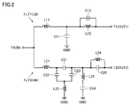
- FIG. 2 is a diagram showing an equivalent circuit of an example of the filter device (diplexer) 100 in FIG.
- the filter FLT1 is connected between the antenna terminal TA and the first terminal T1.
- the filter FLT2 is connected between the antenna terminal TA and the second terminal T2.
- the filter FLT1 includes inductors L11 and L12 constituting a series arm circuit, a capacitor C12, and a capacitor C11 constituting a parallel arm circuit.
- the inductor L11 is connected to the antenna terminal TA, and the inductor L12 is connected between the inductor L11 and the first terminal T1. That is, the inductors L11 and L12 are connected in series between the antenna terminal TA and the first terminal T1.
- the capacitor C11 is connected between the connection node between the inductor L11 and the inductor L12 and the ground terminal GND.
- the capacitor C12 is connected in parallel with the inductor L12.
- the filter FLT2 includes inductors L21, L24 and capacitors C21, C25 forming a series arm circuit, and inductors L22, L23 and capacitors C22 to C24 forming a parallel arm circuit.
- One end of the inductor L21 is connected to the antenna terminal TA, and the other end is connected to the capacitor C21 at one end.
- the capacitor C25 is connected between the other end of the capacitor C21 and the second terminal T2.
- the inductor L24 is connected in parallel to the capacitor C25.
- One end of the capacitor C22 is connected to a connection node between the inductor L21 and the capacitor C21.
- the other end of the capacitor C22 is connected to the ground terminal GND via the inductor L22.
- One end of the capacitor C23 is connected to a connection node between the capacitor C21 and the capacitor C25.
- the other end of the capacitor C23 is connected to the ground terminal GND via the inductor L22.
- One end of the inductor L23 is connected to the connection node between the capacitor C21 and the capacitor C25.
- the other end of the inductor L23 is connected to the ground terminal GND via the capacitor C24.
- the filter FLT2 is a resonance composed of an inductor L21 for trapping, an LC resonator composed of an inductor L22 and capacitors C21 to C23, a resonator composed of an inductor L23 and a capacitor C24, and an inductor L24 and a capacitor C25. Depending on the capacitor, it functions as a band path filter.
- the pass band of the filter FLT1 is set to around 0 to 960 MHz, and the pass band of the filter FLT2 is set to around 1427 MHz to 2690 MHz. Therefore, in the filter device 100, the filter FLT2 functions as a high-pass filter.
- FIG. 3 is a perspective view showing the inside of the filter device 100 of FIG. 2, and FIG. 4 is an exploded perspective view showing an example of the laminated structure of the filter device 100.
- FIG. 5 is a diagram for explaining the arrangement of the inductors in the filter device 100, and specifically, is a plan view in which the dielectric layer LY2 to the dielectric layer LY8 in FIG. 4 are overlapped.
- the filter device 100 includes a rectangular parallelepiped or substantially rectangular parallelepiped main body 110 formed by stacking a plurality of dielectric layers LY1 to LY17 along a predetermined direction.
- the direction in which a plurality of dielectric layers LY1 to LY17 are stacked is defined as the stacking direction.
- Each dielectric layer of the main body 110 is formed of, for example, a ceramic such as low temperature co-fired ceramics (LTCC: Low Temperature Co-fired Ceramics) or a resin.
- LTCC Low Temperature Co-fired Ceramics
- a plurality of electrodes provided in each dielectric layer and a plurality of vias provided between the dielectric layers form an inductor and a capacitor for forming the filters FLT1 and FLT2.
- the dielectric of the main body 110 is omitted, and only the wiring pattern provided inside, the via, and the conductor of the terminal are shown.
- the term "via” refers to a conductor formed in a dielectric layer for connecting electrodes provided in different dielectric layers. Vias are formed, for example, by conductive paste, plating, and / or metal pins.
- the stacking direction of the main body 110 is defined as the "Z-axis direction", the direction perpendicular to the Z-axis direction and along the long side of the main body 110 is defined as the "X-axis direction”, and the short side of the main body 110 is used.
- the direction along the line is defined as the "Y-axis direction”.
- the positive direction of the Z axis in each figure may be referred to as an upper side, and the negative direction may be referred to as a lower side.
- a directional mark DM for specifying the direction of the filter device 100 is arranged on the first main surface 111 (dielectric layer LY1) of the main body 110.
- the second main surface 112 (dielectric layer LY17) of the main body 110 has an antenna terminal TA, a first terminal T1, a second terminal T2, and a ground terminal, which are external terminals for connecting the filter device 100 and an external device. GND is arranged.
- Each external terminal is a flat plate-shaped electrode, and is an LGA (Land Grid Array) terminal regularly arranged on the second main surface 112 of the main body 110.
- LGA Line Grid Array
- the filter FLT1 on the low band side is arranged on the left side (negative direction of the X axis) of the main body 110, and the high on the right side (positive direction of the X axis).
- the filter FLT2 on the band side is arranged.
- the antenna terminal TA arranged on the second main surface 112 is connected to the branch point PB1 between the filter FLT1 and the filter FLT2 in the dielectric layer LY2 via the vias VA1 and VA2 and the flat plate electrode PA1. ing.
- the via VA1 and the via VA2 are offset by the flat plate electrode PA1 provided on the dielectric layer LY16.
- a linear plate electrode PL1 extending in the negative direction of the X-axis from the branch point PB1 is connected to the branch point PB1.
- a via VL1 is connected to the end of the flat plate electrode PL1.
- the flat plate electrode PL1 is connected to one end of the strip-shaped flat plate electrode PL1A provided on the dielectric layer LY8 via the via VL1.
- a via VL1A is connected to the other end of the flat plate electrode PL1A.
- the flat plate electrode PL1A is connected to one end of the linear flat plate electrode PL1B provided on the dielectric layer LY2 via the via VL1A.
- the flat plate electrode PL1B extends in the X-axis direction in the dielectric layer LY2, and the via VL1B is connected to the other end.
- the flat plate electrode PL1B is connected to one end of the strip-shaped flat plate electrode PL1C provided on the dielectric layer LY8 via the via VL1B.
- Via VL1C is connected to the other end of the flat plate electrode PL1C.
- the flat plate electrode PL1C is connected to one end of the linear flat plate electrode PL1D provided on the dielectric layer LY2 via the via VL1C.
- the flat plate electrode PL1D extends in the X-axis direction in the dielectric layer LY2, and the via VL1D is connected to the other end.
- the flat plate electrode PL1D is connected to one end of the strip-shaped flat plate electrode PL1E provided on the dielectric layer LY8 via the via VL1D.
- a via VL1E is connected to the other end of the flat plate electrode PL1E.
- the flat plate electrode PL1E is connected to one end of the linear flat plate electrode PL1F provided on the dielectric layer LY2 via the via VL1E.
- the flat plate electrode PL1F extends in the X-axis direction in the dielectric layer LY2, and the via VL1F is connected to the other end.
- the flat plate electrode PL1F is connected to one end of the linear flat plate electrode P1 provided on the dielectric layer LY8 via the via VL1F.
- the inductor L11 in FIG. 2 is configured by the flat plate electrodes PA1, PL1 to PL1F and vias VA1, VA2, VL1 to VL1F.
- the flat plate electrode P1 extends in the Y-axis direction in the dielectric layer LY8, and the via VL2 is connected to the other end.
- the flat plate electrode P1 is connected to one end of the linear flat plate electrode PL2 provided on the dielectric layer LY2 via the via VL2.
- the flat plate electrode PL2 extends in the X-axis direction in the dielectric layer LY2, and the via VL2A is connected to the other end.
- the flat plate electrode PL2 is connected to one end of the linear flat plate electrode PL2A provided on the dielectric layer LY8 via the via VL2A.
- Via VL2B is connected to the other end of the flat plate electrode PL2A.
- the flat plate electrode PL2A is connected to one end of the linear flat plate electrode PL2B provided on the dielectric layer LY2 via the via VL2B.
- the flat plate electrode PL2B extends in the X-axis direction in the dielectric layer LY2, and the via VL2C is connected to the other end.
- the flat plate electrode PL2B is connected to the capacitor electrode PC1 provided on the dielectric layer LY16 and the capacitor electrode PC3 provided on the dielectric layer LY14 via the via VL2C.
- the via VL2C is offset in the dielectric layer LY9.
- the capacitor electrode PC1 is connected to the first terminal T1 by the via V1.
- the inductor L12 in FIG. 2 is configured by the flat plate electrodes PL2 to PL2B, vias VL2 to VL2C, V1 and the capacitor electrode PC1.
- each of the capacitor electrodes PC1 and PC3 is arranged so that a part thereof overlaps with the capacitor electrode PC2 provided in the dielectric layer LY15.
- the capacitor C12 in FIG. 2 is configured by the capacitor composed of the capacitor electrode PC1 and the capacitor electrode PC2, and the combined capacity of the formed capacitor by the capacitor electrode PC2 and the capacitor electrode PC3.
- a part of the capacitor electrode PC2 has a shape so as to overlap with the flat plate electrode PG provided on the dielectric layer LY16 when the main body 110 is viewed in a plan view from the stacking direction.
- the flat plate electrode PG is connected to the ground terminal GND by vias VG1 and VG2. Therefore, the capacitor C11 in FIG. 2 is configured by the capacitor electrode PC2 and the flat plate electrode PG.
- One end of the strip-shaped flat plate electrode PL3 wound around the axis (Z axis) in the stacking direction of the main body 110 is connected to the branch point PB1.
- a via VL3 is connected to the other end of the flat plate electrode PL3.
- the flat plate electrode PL3 is connected to one end of the strip-shaped flat plate electrode PL3A provided on the dielectric layer LY3 via the via VL3.
- the flat plate electrode PL3A is also an electrode wound around the Z axis like the flat plate electrode PL3, and the via VL3A is connected to the other end.
- the flat plate electrode PL3A is connected to one end of the strip-shaped flat plate electrode PL3B provided on the dielectric layer LY4 via the via VL3A.
- the flat plate electrode PL3B is also an electrode wound around the Z axis like the flat plate electrode PL3 and the like, and the via VL3B is connected to the other end.
- the flat plate electrode PL3B is connected to one end of the strip-shaped flat plate electrode PL3C provided on the dielectric layer LY6 via the via VL3B.
- the flat plate electrode PL3C has a substantially C shape, and a via VL3C is connected to the other end.
- the via VL3C is connected to the capacitor electrode PC11 provided on the dielectric layer LY10 and the capacitor electrode PC10 provided on the dielectric layer LY11.
- the inductor L21 in FIG. 2 is configured by the flat plate electrodes PA1, PL3 to PL3C and vias VA1, VA2, VL3 to VL3C.
- the capacitor electrode PC 10 is arranged so that a part of the main body 110 overlaps with the capacitor electrode PC 7 provided in the dielectric layer LY12 when the main body 110 is viewed in a plan view from the stacking direction.
- the capacitor electrodes PC7 and PC10 constitute the capacitor C22 in FIG. 2.
- the capacitor electrode PC7 is connected to one end of the strip-shaped flat plate electrode PL4 provided on the dielectric layer LY6 by the via VL4.
- the flat plate electrode PL4 has a substantially L-shape, and a via VL4A is connected to the other end.
- the flat plate electrode PL4 is connected to one end of the strip-shaped flat plate electrode PL4A provided on the dielectric layer LY5 via the via VL4A.
- the flat plate electrode PL4A is an electrode wound around the Z axis, and a via VL4B is connected to the other end.
- the flat plate electrode PL4A is connected to one end of the strip-shaped flat plate electrode PL4B provided on the dielectric layer LY4 via the via VL4B.
- the flat plate electrode PL4B is also an electrode wound around the Z axis, and a via VL4C is connected to the other end.
- the flat plate electrode PL4B is connected to one end of the strip-shaped flat plate electrode PL4C provided on the dielectric layer LY3 via the via VL4C.
- the flat plate electrode PL4C is also an electrode wound around the Z axis, and a via VL4D is connected to the other end.
- the flat plate electrode PL4C is connected to one end of the linear flat plate electrode PL4D provided on the dielectric layer LY2 via the via VL4D.
- the flat plate electrode PL4D extends in the Y-axis direction, and the via VL4E is connected to the other end.
- the via VL4E is offset in the dielectric layer LY7 and is connected to the capacitor electrode PC5 provided in the dielectric layer LY14 and the flat plate electrode PG provided in the dielectric layer LY16.
- the flat plate electrode PG is connected to the ground terminal GND of the dielectric layer LY17. Therefore, the inductor L22 in FIG. 2 is configured by the flat plate electrodes PG, PL4 to PL4D and vias VG1, VG2, VL4 to VL4E.
- a part of the capacitor electrode PC 5 is arranged so as to overlap the capacitor electrode PC 6 provided on the dielectric layer LY13 when the main body 110 is viewed in a plan view from the stacking direction.
- the capacitor electrode PC5 and the capacitor electrode PC6 constitute the capacitor C23 in FIG. 2.
- the capacitor electrode PC6 is connected to the capacitor electrode PC9 provided in the dielectric layer LY11 by the via VL5.
- Each of the capacitor electrode PC6 and the capacitor electrode PC9 is arranged so as to partially overlap the capacitor electrodes PC7 and PC8 provided in the dielectric layer LY12 when the main body 110 is viewed in a plan view from the stacking direction.
- the capacitor electrodes PC6 and PC9 and the capacitor electrodes PC7 constitute the capacitor C21 in FIG. 2. Further, the capacitor C25 in FIG. 2 is configured by the capacitor electrodes PC6 and PC9 and the capacitor electrode PC8.
- the capacitor electrode PC9 is connected to the strip-shaped flat plate electrodes PL5 and PL6 at the branch point PB2 of the dielectric layer LY2 via the via VL5A.
- the flat plate electrode PL5 has a substantially L-shape.
- a via VL5B is connected to the end of the flat plate electrode PL5 opposite to the branch point PB2.
- the flat plate electrode PL5 is connected to one end of the strip-shaped flat plate electrode PL5A provided on the dielectric layer LY3 via the via VL5B.
- the flat plate electrode PL5A is an electrode wound around the Z axis, and a via VL5C is connected to the other end.
- the flat plate electrode PL5A is connected to one end of the strip-shaped flat plate electrode PL5B provided on the dielectric layer LY4 via the via VL5C.
- the flat plate electrode PL5B is also an electrode wound around the Z axis like the flat plate electrode PL5A, and the via VL5D is connected to the other end.
- the flat plate electrode PL5B is connected to one end of the strip-shaped flat plate electrode PL5C provided on the dielectric layer LY5 via the via VL5D.
- the flat plate electrode PL5C is also an electrode wound around the Z axis like the flat plate electrode PL5A and the like, and the via VL5E is connected to the other end.
- the flat plate electrode PL5C is connected to the capacitor electrode PC4 provided in the dielectric layer LY15 via the via VL5E.
- the inductor L23 in FIG. 2 is configured by the flat plate electrodes PL5 to PL5C, the capacitor electrodes PC9, and the vias VL5 to VL5E.
- the capacitor C24 in FIG. 2 is configured by the capacitor electrode PC4 and the flat plate electrode PG.
- the flat plate electrode PL6 is a linear electrode extending in the Y-axis direction from the branch point PB2 of the dielectric layer LY2.
- the via VL6 is connected to the end opposite to the branch point PB2.
- the flat plate electrode PL6 is connected to one end of the strip-shaped flat plate electrode PL6A provided on the dielectric layer LY7 via the via VL6.
- a via VL6A is connected to the other end of the flat plate electrode PL6A.
- the flat plate electrode PL6A is connected to one end of the flat plate electrode PL6B provided on the dielectric layer LY2 via the via VL6A.
- the flat plate electrode PL6B is a linear electrode extending in the Y-axis direction, and a via VL6B is connected to the other end.
- the flat plate electrode PL6B is connected to one end of the strip-shaped flat plate electrode PL6C provided on the dielectric layer LY7 via the via VL6B.
- a via VL6C is connected to the other end of the flat plate electrode PL6C.
- the flat plate electrode PL6C is connected to the capacitor electrode PC8 provided on the dielectric layer LY12 and the flat plate electrode PA2 provided on the dielectric layer LY16 via the via VL6C.
- the flat plate electrode PA2 is connected to the second terminal T2 provided in the dielectric layer LY17 via the via V2.
- the plate electrode PA2, PL6 to PL6C and vias VL6 to VL6C constitute the inductor L24 in FIG. 2.
- FIG. 5 is a plan view in which the dielectric layer LY2 to the dielectric layer LY8 in the filter device 100 are overlapped.
- the filter FLT1 of the low-pass filter is arranged on the left side (negative direction of the X axis) side of FIG. 5 in the main body 110, and the filter FLT1 of the low-pass filter is arranged on the right side (X axis) of FIG.
- the filter FLT2 of the high-pass filter is arranged on the side (in the positive direction of).
- the inductors L11 and L12 of the filter FLT1 are arranged in the region RG1 (first region) of the main body 110. Further, the inductors L21 to L24 of the filter FLT2 are arranged in the region RG2 (second region) of the main body 110.
- the inductors L11 and L12 of the filter FLT1 are configured as a vertical coil including a flat plate electrode and vias.
- the winding shafts of the inductors L11 and L12 are in the Y-axis direction, and are wound for two or more turns in order to secure a desired inductance.
- the inductor L11 is wound counterclockwise (CCW) toward the positive direction of the Y axis, and the inductor L12 is wound clockwise (CW) toward the positive direction of the Y axis. Therefore, a magnetic field is generated in the Y-axis direction by the inductors L11 and L12.
- the inductors L21, L22, and L23 are helical coils in which a planar coil whose winding direction is the stacking direction (Z-axis direction) of the main body 110 is connected by vias. Further, the inductor L24 is a vertical coil having a winding axis in the X-axis direction. Therefore, the inductors L21, L22, and L23 generate a magnetic field in the Z-axis direction, and the inductor L24 generates a magnetic field in the X-axis direction.
- the inductors L21 and L23 arranged facing the filter FLT1 are wound for two or more turns.
- the direction of the magnetic field generated by the filter FLT1 is orthogonal to the direction of the magnetic field generated by the filter FLT2 when viewed in a plan view from the stacking direction of the main body 110, and is opposite to each other. Not suitable for filter coils.
- the virtual line CL1 drawn in the filter FLT1 from the center of the plate electrode constituting the inductor in the direction orthogonal to the extending direction does not intersect with the inductors L21 to L24 of the filter FLT2 and is virtual.
- the angle formed by the direction in which the line CL1 extends (second direction) and the direction from the region RG1 toward the region RG2 (first direction) is 90 °.
- the magnetic field generated by the filter FLT1 does not interfere with the magnetic field generated by the inductors L21 and L23 of the filter FLT2 arranged at the positions facing the region RG1. This makes it possible to suppress the magnetic coupling between the inductors between the filter FLT1 and the filter FLT2.
- FIG. 6 is a diagram for explaining the arrangement of inductors of each filter in the filter device 100X of Comparative Example 1.
- the inductors L11X and L12X included in the filter FLT1X on the low band side include a flat coil having a winding axis in the Z-axis direction.
- the high band side is the same as the filter FLT2 of the first embodiment.
- the magnetic field generated by the inductors L11X and L12X of the filter FLT1X may interfere with the magnetic field generated by the inductors L21 and L23 of the filter FLT2 arranged at positions facing the region RG1, and magnetic coupling between the inductors may occur. ..
- FIG. 7 is a diagram for explaining the passing characteristics of the filter device 100 of the first embodiment and the filter device 100X of the comparative example 1.
- the horizontal axis shows the frequency
- the vertical axis shows the insertion loss.
- the solid lines LN10 and LN20 show the insertion loss of the filters FLT1 and FLT2 in the filter device 100 of the first embodiment, respectively.
- the broken lines LN11 and LN21 indicate the insertion loss of the filters FLT1X and FLT2 in the filter device 100X of Comparative Example 1, respectively.
- the Q value of the inductor is improved by suppressing the magnetic coupling, so that the filter device 100 of the first embodiment is compared with the case of the filter device 100X of Comparative Example 1. Insertion loss has improved.
- the inductor L11 on the low band side is an element that can be directly seen from the filter FLT2 on the high band side. Therefore, on the high band side, the configuration of the filter device 100 and the filter device 100X is the same, but the Q value of the inductor L11 on the low band side is improved, so that the insertion loss of the filter FLT2 on the high band side is also compared.
- the filter device 100 of the first embodiment is slightly improved over the filter device 100X of the first embodiment.
- FIG. 8 is a diagram for explaining the arrangement of inductors of each filter in the filter device 100Y of Comparative Example 2 having different configurations.
- each of the inductors L11Y and L12Y included in the filter FLT1Y on the low band side is a vertical coil like the filter device 100 of the first embodiment.
- the inductors L11Y and L12Y are arranged so that the winding axis is in the X-axis direction. That is, in the inductors L11Y and L12Y, the angle between the virtual lines CL2 and CL2A drawn in the direction orthogonal to the extending direction of the flat plate electrode from the center of the extending direction and the direction from the region RG1 to the region RG2 is 0 °. be.
- the direction of the magnetic field generated by each of the inductors L11Y and L12Y is the direction of the filter FLT2. Therefore, the magnetic field generated by the inductors L11Y and L12Y of the filter FLT1Y interferes with the magnetic field generated by the inductors L21 and L23 of the filter FLT2 arranged at the positions facing the region RG1, and the inductors may be magnetically coupled to each other.
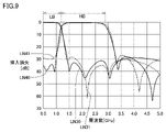
- FIG. 9 is a diagram for explaining the passing characteristics in the filter device 100 of the first embodiment and the filter device 100Y of the comparative example 2.
- the horizontal axis shows the frequency
- the vertical axis shows the insertion loss.
- the solid lines LN30 and LN40 show the insertion loss of the filters FLT1 and FLT2 in the filter device 100 of the first embodiment, respectively.
- the broken lines LN31 and LN41 indicate the insertion loss of the filters FLT1Y and FLT2 in the filter device 100Y of Comparative Example 2, respectively.
- the insertion loss in the pass band on the low band side and the high band side is almost the same as that of the filter device 100 and the filter device 100Y.
- the filter device 100Y of Comparative Example 2 since the inductors of each other are magnetically coupled to each other, the amount of attenuation of the attenuation pole in the vicinity of the pass band on the low band side (near 1.5 GHz) and the passage on the high band side. The amount of attenuation of the attenuation pole in the vicinity of the band (near 1.0 GHz) is small.
- the attenuation characteristic in the non-passband is improved as compared with the case of the filter device 100Y of the comparative example 2.
- the inductor of the filter on the low band side is composed of a vertical coil, and the filter on the high band side is used as the filter on the low band side.
- the low-band side inductor is configured as a vertical coil and the high-band side inductor facing the low-band side filter is configured as a planar coil has been described.
- the low band side may be composed of a flat coil
- the high band side may be composed of a vertical coil.
- the filter on the low band side includes two inductors
- the number of inductors included in the filter on the low band side may be three or more.
- the "filter FLT1" and “filter FLT2" in the first embodiment correspond to the “first LC filter” and the “second LC filter” in the present disclosure.
- the “inductor L11” and “inductor L12” in the first embodiment correspond to the "first inductor” and the “second inductor” in the present disclosure.
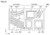
- FIG. 10 is a diagram for explaining the arrangement of inductors of each filter in the filter device 100A according to the second embodiment.
- the filter device 100A has a configuration in which the filter FLT1 on the low band side in the first embodiment is replaced with the filter FLT1A.
- the filter FLT2 on the high band side is the same as that of the filter device 100.
- the description of the elements overlapping with the filter device 100 will not be repeated.
- the low band side filter FLT1A includes inductors L11A and L12A configured as vertical coils.
- the inductor L11A is arranged so that the virtual line CL3 drawn in a direction orthogonal to the extending direction from the center of the extending direction of the flat plate electrode is inclined from the Y-axis direction when viewed in a plan view from the stacking direction of the main body 110. ing. More specifically, the angle ⁇ formed by the direction of the virtual line CL3 (that is, the direction of the winding axis) and the direction from the region RG1 toward the region RG2 is 45 ° or more and 90 ° or less (45 ° ⁇ ⁇ ⁇ 90).
- the inductor L11A is arranged so as to be. At this time, the virtual line CL3 does not intersect with the inductors L21 to L24 included in the filter FLT2.
- the inductor L12A is arranged so that the virtual line CL3A is in the Y-axis direction.
- the inductor on the high band side configured as a planar coil in the direction of the magnetic field formed by the inductor.
- the non-arranged configuration suppresses the magnetic coupling between the low-band side inductor and the high-band side inductor. Therefore, it is possible to suppress the deterioration of the filter characteristics in the diplexer.
- FIG. 11 is a diagram for explaining the arrangement of inductors of each filter in the filter device 100B according to the third embodiment.
- the filter device 100B has a configuration in which the filter FLT2 on the high band side in the first embodiment is replaced with the filter FLT2B.
- the filter FLT1 on the low band side is the same as that of the filter device 100. In the filter device 100B, the description of the elements overlapping with the filter device 100 will not be repeated.
- the inductors L23 and L24 of the filter FLT2 of the filter device 100 are replaced with the inductors L23B and L24B.
- the inductor L23B is a planar coil, is adjacent to the inductors L21 and L22 in the positive direction of the Y axis, and is further arranged facing the region RG1.
- the inductor L24B is a vertical coil composed of a flat plate electrode extending in the X-axis direction and a via extending in the stacking direction of the main body 110.
- the direction of the winding axis of the inductor L24B is the Y-axis direction.
- the inductor L24B is arranged adjacent to the inductor L23B in the positive direction of the Y axis. In other words, the inductor L23B is arranged between the inductor L21 and the inductor L24B.
- the negative end of the inductor L24B on the X-axis faces the region RG1 of the filter FLT1 on the low band side.
- the distance between the inductor L24B and the region RG1 is longer than the distance between the inductor L21 and the region RG1 and the distance between the inductor L23B and the region RG1.
- the distance between the low-band side inductors L11 and L12 and the high-band side inductor L24B is preferably 50 ⁇ m or more.
- the virtual line CL1 drawn in the direction orthogonal to the extending direction from the center of the extending direction of the flat plate electrodes constituting the inductors L11 and L12 which are vertical coils is the inductors L21, L22, L23B of the filter FLT2B. , Does not intersect with L24B.
- the virtual line CL4 drawn in the direction orthogonal to the extending direction from the center of the extending direction of the flat plate electrode constituting the inductor L24B which is a vertical coil intersects the inductors L11 and L12. not.
- the inductors L11 and L12 in the filter FLT1 By arranging the inductors L11 and L12 in the filter FLT1 in this way, the magnetic field generated by the filter FLT1 does not interfere with the magnetic field generated by the inductors L21 and L23B of the filter FLT2B arranged at the positions facing the region RG1. Further, since the inductor L24B, which is a vertical coil of the filter FLT2B, is arranged at a position farther from the region RG1 than the inductors L21 and L23B, the magnetic field generated by the inductor L24B and the magnetic field generated by the inductors L11 and L12 of the filter FLT1. Interference with can be suppressed.
- the inductor L24B configured as a vertical coil in the filter FLT2B is arranged at a position facing the region RG1 of the filter FLT1, the inductor L24B is located in the region RG1 rather than the inductor L21, 23B of the flat coil. By arranging it at a distant position, it is possible to suppress the magnetic coupling between the vertical coils and suppress the decrease in the isolation between the filters FLT1 and FLT2B.
- the inductance value of a coil is proportional to the air core diameter of the coil and inversely proportional to the length of the coil. Therefore, when the same inductance value is realized, the overall line length of the inductor can be shortened by increasing the air core diameter as compared with the inductor L24 of the first embodiment, as in the inductor L24B. As a result, the conductor loss in the inductor L24B is reduced, so that the insertion loss of the filter FLT2B can be reduced.
- the filter device 100B of the third embodiment it is possible to suppress the deterioration of the filter characteristics in the diplexer.
- the inductors L11 and L12 of the filter FLT1 and the inductor L24B of the filter FLT2B are configured as a vertical coil whose winding axis is in the Y-axis direction.
- the virtual line drawn from the center of the flat plate electrode constituting the vertical coil in the direction orthogonal to the extending direction can be arranged so as not to intersect the inductor of the other filter, these The inductors L11, l12, and L24B may be arranged so that the winding axis is inclined from the Y-axis direction, as in the inductor L11A in the filter device 100A of the second embodiment.
- 10 communication device 20 high frequency front end circuit, C11, C12, C21 to C25 capacitors, 100, 100A, 100B, 100X, 100Y filter device, 110 main body, 111, 112 main surface, ANT antenna device, CL1, CL2, CL2A, CL3, CL3A, CL4 virtual line, DM directional mark, FLT1, FLT1A, FLT1X, FLT1Y, FLT2, FLT2B filter, GND ground terminal, IN input terminal, L11, L11A, L11X, L11Y, L12, L12A, L12X, L12Y, L21 to L24, L23B, L24B inductor, LNA1, LNA2 amplifier circuit, LY1 to LY17 dielectric layer, OUT1, OUT2 output terminal, P1, PA1, PA2, PG, PL1, PL1A to PL1F, PL2, PL2A, PL2B, PL3 PL3A to PL3C, PL4, PL4A to PL4D
Landscapes
- Engineering & Computer Science (AREA)
- Power Engineering (AREA)
- Microelectronics & Electronic Packaging (AREA)
- Filters And Equalizers (AREA)
Abstract
フィルタ(100)は、本体(110)と、異なる通過帯域を有するフィルタ(FLT,FLT2)を備える。本体(110)において、フィルタ(FLT1)のインダクタは領域(RG1)に配置され、フィルタ(FLT2)のインダクタは領域(RG2)に配置される。フィルタ(FLT1)に含まれるインダクタは、本体に設けられた平板電極と、本体の法線方向に延在するビアとを含む縦型コイルである。フィルタ(FLT2)において、領域(RG1)に面する位置に配置されるインダクタは、本体(110)の法線方向を巻回軸とする平面コイルである。本体(110)の法線方向から平面視した場合に、フィルタ(FLT1)における平板電極の延在方向の中央から、当該延在方向に直交する方向に描いた仮想線(CL1)は、フィルタ(FLT2)のインダクタと交差しない。
Description
本開示は、フィルタ装置およびそれを搭載した高周波フロントエンド回路に関し、より特定的には、2つのLCフィルタを含むダイプレクサにおける通過特性を向上させるための技術に関する。
特表2019-507972号公報(特許文献1)には、LC回路で構成されたハイバンドフィルタおよびローバンドフィルタを備えたマルチプレクサが開示されている。特表2019-507972号公報(特許文献1)のマルチプレクサにおいては、ハイバンドフィルタのインダクタが基板の表面に2Dスパイラルインダクタとして構成され、ローバンドフィルタのインダクタが基板の内部の層に3Dインダクタとして構成されている。
また、特開平11-40920号公報(特許文献2)には、複数のインダクタが集積化された複合部品において、隣接するインダクタによって発生する磁束が互いに略直交するように、インダクタが配置された構成が開示されている。
しかしながら、特表2019-507972号公報(特許文献1)および特開平11-40920号公報(特許文献2)に開示された構成においては、隣接して配置されたフィルタに含まれるインダクタにおいて、一方のインダクタの空芯径を貫く磁束が他方のインダクタと干渉しているため、2つのインダクタ同士の磁気結合が生じ得る。
複数のLCフィルタを含むフィルタ装置(ダイプレクサ,マルチプレクサ)において、異なるフィルタ間のインダクタ同士が磁気結合すると、Q値の低下および/またはアイソレーションの劣化が生じてしまい、フィルタ特性が低下するおそれがある。
本開示は、このような課題を解決するためになされたものであって、その目的は、複数のLCフィルタを含んで構成されるフィルタ装置において、フィルタ特性の低下を抑制することである。
本開示の第1の局面に係るフィルタ装置は、本体と、第1通過帯域を有する第1フィルタと、第1通過帯域とは異なる第2通過帯域を有する第2フィルタとを備える。本体の法線方向から平面視した場合に、第1フィルタに含まれるインダクタは第1領域に配置され、第2フィルタに含まれるインダクタは第1領域に隣接する第2領域に配置される。第1フィルタおよび第2フィルタの各々は、少なくとも1つのインダクタを含む。第1フィルタに含まれるインダクタは、本体に設けられた平板電極と、本体の法線方向に延在するビアとを含む縦型コイルである。第2フィルタにおいて、第1領域に面する位置に配置されるインダクタは、本体の法線方向を巻回軸とする平面コイルである。本体の法線方向から平面視した場合に、第1フィルタにおける平板電極の延在方向の中央から、当該延在方向に直交する方向に描いた仮想線は、第2フィルタに含まれるインダクタと交差しない。
本開示の第2の局面に掛かるフィルタ装置は、本体と、第1通過帯域を有する第1フィルタと、第1通過帯域とは異なる第2通過帯域を有する第2フィルタとを備える。第1フィルタおよび第2フィルタの各々は、少なくとも1つのインダクタを含む。本体の法線方向から平面視した場合に、第1フィルタに含まれるインダクタは第1領域に配置され、第2フィルタに含まれるインダクタは第1領域に隣接する第2領域に配置される。第1フィルタに含まれるインダクタは、本体に設けられた平板電極と、本体の法線方向に延在するビアとを含む縦型コイルである。第2フィルタにおいて、第1領域に面する位置に配置されるインダクタは、縦型コイル、および、本体の法線方向を巻回軸とする平面コイルを含む。第2フィルタの縦型コイルと第1領域との間の距離は、上記の平面コイルと第1領域との間の距離よりも遠い。本体の法線方向から平面視した場合に、(i)第1フィルタにおける平板電極の延在方向の中央から、当該延在方向に直交する方向に描いた第1仮想線は、第2フィルタに含まれるインダクタと交差しておらず、(ii)第2フィルタにおける平板電極の延在方向の中央から、当該延在方向に直交する方向に描いた第2仮想線は、第1フィルタに含まれるインダクタと交差しない。
本開示によるフィルタ装置においては、本体において隣接する領域に2つフィルタ(第1フィルタ,第2フィルタ)が配置されている。第1フィルタのインダクタは、平板電極およびビアで構成された縦型コイルである。第2フィルタにおいて、第1フィルタに面して配置されるインダクタは平面コイルである。そして、第1フィルタにおける平板電極の延在方向の中央から、当該延在方向に直交する方向に描いた仮想線は、第2フィルタに含まれるインダクタと交差していない。このような構成とすることによって、一方のフィルタのインダクタによって生じる磁界が他方のフィルタのインダクタと干渉することを防止できるので、インダクタ同士の磁気結合を抑制することができる。したがって、フィルタ特性の低下を抑制することができる。
以下、本開示の実施の形態について、図面を参照しながら詳細に説明する。なお、図中同一または相当部分には同一符号を付してその説明は繰り返さない。
[実施の形態1]
(通信装置の基本構成)
図1は、実施の形態に従うフィルタ装置100が適用された高周波フロントエンド回路20を含む通信装置10のブロック図である。高周波フロントエンド回路20は、アンテナ装置ANTで受信された高周波信号を、予め定められた複数の周波数帯域に分波して後続の処理回路へ伝達する。高周波フロントエンド回路20は、たとえば、携帯電話、スマートフォンあるいはタブレットなどの携帯端末や、通信機能を備えたパーソナルコンピュータなどの通信装置に用いられる。
(通信装置の基本構成)
図1は、実施の形態に従うフィルタ装置100が適用された高周波フロントエンド回路20を含む通信装置10のブロック図である。高周波フロントエンド回路20は、アンテナ装置ANTで受信された高周波信号を、予め定められた複数の周波数帯域に分波して後続の処理回路へ伝達する。高周波フロントエンド回路20は、たとえば、携帯電話、スマートフォンあるいはタブレットなどの携帯端末や、通信機能を備えたパーソナルコンピュータなどの通信装置に用いられる。
図1を参照して、通信装置10は、フィルタ装置100を含む高周波フロントエンド回路20と、RF信号処理回路(以下、「RFIC」とも称する。)30とを含む。図1に示される高周波フロントエンド回路20は、受信系フロントエンド回路である。高周波フロントエンド回路20は、フィルタ装置100と、増幅回路LNA1,LNA2とを含む。
フィルタ装置100は、互いに異なる周波数範囲を通過帯域とするフィルタFLT1(第1フィルタ)およびフィルタFLT2(第2フィルタ)を含むダイプレクサである。以降の説明においては、フィルタ装置100を「ダイプレクサ」と称する場合がある。
フィルタFLT1は、共通端子であるアンテナ端子TAと、第1端子T1との間に接続される。フィルタFLT1は、ローバンド(LB)群の周波数範囲を通過帯域とし、ハイバンド(HB)群の周波数範囲を非通過帯域とするローパスフィルタである。フィルタFLT2は、アンテナ端子TAと第2端子T2との間に接続される。フィルタFLT2は、ハイバンド群の周波数範囲を通過帯域とし、ローバンド群の周波数範囲を非通過帯域とするハイパスフィルタである。なお、フィルタFLT1およびフィルタFLT2は、バンドパスフィルタであってもよい。
フィルタFLT1,FLT2の各々は、アンテナ装置ANTで受信された高周波信号のうち、各フィルタの通過帯域に対応する高周波信号のみを通過させる。これにより、アンテナ装置ANTからの受信信号を予め定められた複数の周波数帯域の信号に分波する。
増幅回路LNA1,LNA2の各々は、いわゆる低雑音増幅器である。増幅回路LNA1,LNA2は、対応するフィルタを通過した高周波信号を低雑音で増幅し、RFIC30へ伝達する。
RFIC30は、アンテナ装置ANTで送受信された高周波信号を処理するRF信号処理回路である。具体的には、RFIC30は、アンテナ装置ANTから高周波フロントエンド回路20の受信側信号経路を介して入力された高周波信号を、ダウンコンバートなどにより信号処理し、当該信号処理して生成された受信信号をベースバンド信号処理回路(図示せず)へ出力する。
図1のように高周波フロントエンド回路20が受信回路として用いられる場合、フィルタ装置100においては、アンテナ端子TAが入力端子INとなり、第1端子T1および第2端子T2がそれぞれ第1出力端子OUT1および第2出力端子OUT2となる。一方で、高周波フロントエンド回路は送信回路としても用いることができる。この場合には、フィルタ装置100の第1端子T1および第2端子T2の各々が入力端子となり、アンテナ端子TAが共通の出力端子となる。その場合、増幅回路に含まれる増幅器としてパワーアンプが用いられる。
(フィルタ装置の構成)
図2は、図1におけるフィルタ装置(ダイプレクサ)100の一例の等価回路を示す図である。図1で説明したように、フィルタFLT1はアンテナ端子TAと第1端子T1との間に接続されている。また、フィルタFLT2はアンテナ端子TAと第2端子T2との間に接続されている。
図2は、図1におけるフィルタ装置(ダイプレクサ)100の一例の等価回路を示す図である。図1で説明したように、フィルタFLT1はアンテナ端子TAと第1端子T1との間に接続されている。また、フィルタFLT2はアンテナ端子TAと第2端子T2との間に接続されている。
フィルタFLT1は、直列腕回路を構成するインダクタL11,L12およびキャパシタC12と、並列腕回路を構成するキャパシタC11とを含む。インダクタL11はアンテナ端子TAに接続され、インダクタL12はインダクタL11と第1端子T1との間に接続される。すなわち、インダクタL11,L12は、アンテナ端子TAと第1端子T1との間に直列に接続されている。キャパシタC11は、インダクタL11とインダクタL12との間の接続ノードと、接地端子GNDとの間に接続される。キャパシタC12は、インダクタL12に並列に接続される。フィルタFLT1は、これらの構成によって、所定の周波数よりも低い周波数帯域の信号を通過させるローパスフィルタとして機能する。
フィルタFLT2は、直列腕回路を形成するインダクタL21,L24およびキャパシタC21,C25と、並列腕回路を形成するインダクタL22,L23およびキャパシタC22~C24とを含む。インダクタL21の一方端はアンテナ端子TAに接続されており、他方端はキャパシタC21に一方端に接続されている。キャパシタC25は、キャパシタC21の他方端と第2端子T2との間に接続されている。インダクタL24は、キャパシタC25に並列に接続されている。
キャパシタC22の一方端は、インダクタL21とキャパシタC21との間の接続ノードに接続される。キャパシタC22の他方端は、インダクタL22を介して接地端子GNDに接続される。キャパシタC23の一方端は、キャパシタC21とキャパシタC25との間の接続ノードに接続される。キャパシタC23の他方端は、インダクタL22介して接地端子GNDに接続される。
インダクタL23の一方端は、キャパシタC21とキャパシタC25との間の接続ノードに接続される。インダクタL23の他方端は、キャパシタC24を介して接地端子GNDに接続される。
フィルタFLT2は、トラップ用のインダクタL21と、インダクタL22およびキャパシタC21~C23で構成されるLC共振器と、インダクタL23およびキャパシタC24で構成される共振器と、インダクタL24およびキャパシタC25で構成される共振器とによって、バンドパスフィルタとして機能する。
なお、実施の形態1のフィルタ装置100の例においては、フィルタFLT1の通過帯域は0~960MHz付近に設定されており、フィルタFLT2の通過帯域は1427MHz~2690MHz付近に設定されている。そのため、フィルタ装置100においては、フィルタFLT2はハイパスフィルタとして機能する。
次に、図3~図5を用いて、フィルタ装置100の内部構成の詳細について説明する。図3は図2のフィルタ装置100の内部を示す斜視図であり、図4はフィルタ装置100の積層構造の一例を示す分解斜視図である。また、図5は、フィルタ装置100におけるインダクタの配置を説明するための図であり、具体的には、図4における誘電体層LY2~誘電体層LY8を重ね合わせた平面図である。
図3および図4を参照して、フィルタ装置100は、複数の誘電体層LY1~LY17が所定の方向に沿って積み上げられて形成された、直方体または略直方体の本体110を備えている。本体110において、複数の誘電体層LY1~LY17が積み上げられている方向を積層方向とする。本体110の各誘電体層は、たとえば低温同時焼成セラミックス(LTCC:Low Temperature Co-fired Ceramics)などのセラミック、あるいは樹脂により形成されている。本体110の内部において、各誘電体層に設けられた複数の電極、および、誘電体層間に設けられた複数のビアによって、フィルタFLT1,FLT2を構成するためのインダクタおよびキャパシタが構成される。なお、図3~図5においては、本体110の誘電体は省略してあり、内部に設けられる配線パターン、ビアおよび端子の導電体のみが示されている。本明細書において「ビア」とは、異なる誘電体層に設けられた電極を接続するために、誘電体層中に形成される導体を示す。ビアは、たとえば、導電ペースト、めっき、および/または金属ピンなどによって形成される。
以下の説明においては、本体110の積層方向を「Z軸方向」とし、Z軸方向に垂直であって本体110の長辺に沿った方向を「X軸方向」とし、本体110の短辺に沿った方向を「Y軸方向」とする。また、以下では、各図におけるZ軸の正方向を上側、負方向を下側と称する場合がある。
本体110の第1主面111(誘電体層LY1)には、フィルタ装置100の方向を特定するための方向性マークDMが配置されている。本体110の第2主面112(誘電体層LY17)には、当該フィルタ装置100と外部機器とを接続するための外部端子であるアンテナ端子TA、第1端子T1、第2端子T2および接地端子GNDが配置されている。各外部端子は平板状の電極であり、本体110の第2主面112に規則的に配置されたLGA(Land Grid Array)端子である。図3および図4で示した例においては、概略的には、本体110の左側(X軸の負方向)部分にローバンド側のフィルタFLT1が配置され、右側(X軸の正方向)部分にハイバンド側のフィルタFLT2が配置されている。
第2主面112(誘電体層LY17)に配置されたアンテナ端子TAは、ビアVA1,VA2および平板電極PA1を介して、誘電体層LY2においてフィルタFLT1とフィルタFLT2との分岐点PB1に接続されている。ビアVA1およびビアVA2は、誘電体層LY16に設けられた平板電極PA1によってオフセットしている。
まず、ローパスフィルタであるフィルタFLT1の詳細について説明する。分岐点PB1には、分岐点PB1からX軸の負方向に延在する直線状の平板電極PL1が接続されている。平板電極PL1の端部にはビアVL1が接続されている。平板電極PL1は、ビアVL1を介して誘電体層LY8に設けられた帯状の平板電極PL1Aの一方端に接続されている。平板電極PL1Aの他方端にはビアVL1Aが接続されている。平板電極PL1Aは、当該ビアVL1Aを介して、誘電体層LY2に設けられた直線状の平板電極PL1Bの一方端に接続されている。平板電極PL1Bは、誘電体層LY2においてX軸方向に延在しており、他方端にはビアVL1Bが接続されている。平板電極PL1Bは、当該ビアVL1Bを介して、誘電体層LY8に設けられた帯状の平板電極PL1Cの一方端に接続されている。
平板電極PL1Cの他方端にはビアVL1Cが接続されている。平板電極PL1Cは、ビアVL1Cを介して誘電体層LY2に設けられた直線状の平板電極PL1Dの一方端に接続されている。平板電極PL1Dは、誘電体層LY2においてX軸方向に延在しており、他方端にはビアVL1Dが接続されている。平板電極PL1Dは、当該ビアVL1Dを介して、誘電体層LY8に設けられた帯状の平板電極PL1Eの一方端に接続されている。
平板電極PL1Eの他方端にはビアVL1Eが接続されている。平板電極PL1Eは、ビアVL1Eを介して誘電体層LY2に設けられた直線状の平板電極PL1Fの一方端に接続されている。平板電極PL1Fは、誘電体層LY2においてX軸方向に延在しており、他方端にはビアVL1Fが接続されている。平板電極PL1Fは、当該ビアVL1Fを介して、誘電体層LY8に設けられた直線状の平板電極P1の一方端に接続されている。平板電極PA1,PL1~PL1FおよびビアVA1,VA2,VL1~VL1Fによって、図2におけるインダクタL11が構成される。
平板電極P1は、誘電体層LY8においてY軸方向に延在しており、その他方端にはビアVL2が接続されている。平板電極P1は、ビアVL2を介して誘電体層LY2に設けられた直線状の平板電極PL2の一方端に接続されている。平板電極PL2は、誘電体層LY2においてX軸方向に延在しており、他方端にはビアVL2Aが接続されている。平板電極PL2は、当該ビアVL2Aを介して、誘電体層LY8に設けられた直線状の平板電極PL2Aの一方端に接続されている。
平板電極PL2Aの他方端にはビアVL2Bが接続されている。平板電極PL2Aは、ビアVL2Bを介して誘電体層LY2に設けられた直線状の平板電極PL2Bの一方端に接続されている。平板電極PL2Bは、誘電体層LY2においてX軸方向に延在しており、他方端にはビアVL2Cが接続されている。平板電極PL2Bは、当該ビアVL2Cを介して、誘電体層LY16に設けられたキャパシタ電極PC1、および、誘電体層LY14に設けられたキャパシタ電極PC3に接続されている。なお、ビアVL2Cは、誘電体層LY9においてオフセットしている。キャパシタ電極PC1は、ビアV1によって第1端子T1に接続されている。平板電極PL2~PL2B、ビアVL2~VL2C,V1およびキャパシタ電極PC1によって、図2におけるインダクタL12が構成される。
本体110を積層方向から平面視した場合に、キャパシタ電極PC1,PC3の各々は、その一部が誘電体層LY15に設けられたキャパシタ電極PC2と重なるように配置されている。キャパシタ電極PC1とキャパシタ電極PC2とによって構成されるキャパシタ、および、キャパシタ電極PC2とキャパシタ電極PC3によって形構成キャパシタの合成容量によって、図2におけるキャパシタC12が構成される。
また、キャパシタ電極PC2の一部は、本体110を積層方向から平面視した場合に、誘電体層LY16に設けられた平板電極PGとも重なるような形状を有している。平板電極PGは、ビアVG1,VG2によって、接地端子GNDに接続されている。したがって、キャパシタ電極PC2と平板電極PGとによって、図2におけるキャパシタC11が構成される。
次に、ハイパスフィルタであるフィルタFLT2の詳細について説明する。分岐点PB1には、本体110の積層方向の軸(Z軸)周りに巻回された帯状の平板電極PL3の一方端が接続される。平板電極PL3の他方端には、ビアVL3が接続されている。平板電極PL3は、ビアVL3を介して、誘電体層LY3に設けられた帯状の平板電極PL3Aの一方端に接続される。
平板電極PL3Aも、平板電極PL3と同様にZ軸周りに巻回された電極であり、その他方端にはビアVL3Aが接続されている。平板電極PL3Aは、ビアVL3Aを介して、誘電体層LY4に設けられた帯状の平板電極PL3Bの一方端に接続される。平板電極PL3Bも、平板電極PL3等と同様にZ軸周りに巻回された電極であり、その他方端にはビアVL3Bが接続されている。平板電極PL3Bは、ビアVL3Bを介して、誘電体層LY6に設けられた帯状の平板電極PL3Cの一方端に接続される。
平板電極PL3Cは、略C字形状を有しており、他方端にはビアVL3Cが接続されている。ビアVL3Cは、誘電体層LY10に設けられたキャパシタ電極PC11、および、誘電体層LY11に設けられたキャパシタ電極PC10に接続されている。平板電極PA1,PL3~PL3CおよびビアVA1,VA2,VL3~VL3Cによって、図2におけるインダクタL21が構成される。
キャパシタ電極PC10は、本体110を積層方向から平面視した場合に、その一部が誘電体層LY12に設けられたキャパシタ電極PC7と重なるように配置されている。キャパシタ電極PC7,PC10によって、図2のキャパシタC22が構成される。
キャパシタ電極PC7は、ビアVL4によって、誘電体層LY6に設けられた帯状の平板電極PL4の一方端に接続されている。平板電極PL4は、略L字形状を有しており、その他方端にはビアVL4Aが接続されている。平板電極PL4は、ビアVL4Aを介して、誘電体層LY5に設けられた帯状の平板電極PL4Aの一方端に接続されている。平板電極PL4Aは、Z軸周りに巻回された電極であり、その他方端にはビアVL4Bが接続されている。平板電極PL4Aは、ビアVL4Bを介して、誘電体層LY4に設けられた帯状の平板電極PL4Bの一方端に接続されている。
平板電極PL4Bも、Z軸周りに巻回された電極であり、その他方端にはビアVL4Cが接続されている。平板電極PL4Bは、ビアVL4Cを介して、誘電体層LY3に設けられた帯状の平板電極PL4Cの一方端に接続されている。平板電極PL4Cも、Z軸周りに巻回された電極であり、その他方端にはビアVL4Dが接続されている。平板電極PL4Cは、ビアVL4Dを介して、誘電体層LY2に設けられた直線状の平板電極PL4Dの一方端に接続されている。
平板電極PL4Dは、Y軸方向に延在しており、その他方端にはビアVL4Eが接続されている。ビアVL4Eは、誘電体層LY7においてオフセットし、誘電体層LY14に設けられたキャパシタ電極PC5、および、誘電体層LY16に設けられた平板電極PGに接続される。上述のように、平板電極PGは、誘電体層LY17の接地端子GNDに接続されている。したがって、平板電極PG,PL4~PL4DおよびビアVG1,VG2,VL4~VL4Eによって、図2におけるインダクタL22が構成される。
キャパシタ電極PC5の一部は、本体110を積層方向から平面視した場合に、誘電体層LY13に設けられたキャパシタ電極PC6と重なるように配置されている。キャパシタ電極PC5およびキャパシタ電極PC6によって、図2におけるキャパシタC23が構成される。
キャパシタ電極PC6は、ビアVL5によって、誘電体層LY11に設けられたキャパシタ電極PC9に接続されている。キャパシタ電極PC6およびキャパシタ電極PC9の各々は、本体110を積層方向から平面視した場合に、誘電体層LY12に設けられたキャパシタ電極PC7,PC8と部分的に重なるように配置されている。キャパシタ電極PC6,PC9とキャパシタ電極PC7とによって、図2におけるキャパシタC21が構成される。また、キャパシタ電極PC6,PC9とキャパシタ電極PC8とによって、図2におけるキャパシタC25が構成される。
キャパシタ電極PC9は、ビアVL5Aを介して、誘電体層LY2の分岐点PB2において帯状の平板電極PL5,PL6に接続される。平板電極PL5は、略L字形状を有している。平板電極PL5における分岐点PB2とは反対の端部には、ビアVL5Bが接続されている。平板電極PL5は、ビアVL5Bを介して、誘電体層LY3に設けられた帯状の平板電極PL5Aの一方端に接続される。
平板電極PL5Aは、Z軸周りに巻回された電極であり、その他方端にはビアVL5Cが接続されている。平板電極PL5Aは、ビアVL5Cを介して、誘電体層LY4に設けられた帯状の平板電極PL5Bの一方端に接続される。
平板電極PL5Bも、平板電極PL5Aと同様にZ軸周りに巻回された電極であり、その他方端にはビアVL5Dが接続されている。平板電極PL5Bは、ビアVL5Dを介して、誘電体層LY5に設けられた帯状の平板電極PL5Cの一方端に接続される。平板電極PL5Cも、平板電極PL5A等と同様にZ軸周りに巻回された電極であり、その他方端にはビアVL5Eが接続されている。平板電極PL5Cは、ビアVL5Eを介して、誘電体層LY15に設けられたキャパシタ電極PC4に接続される。平板電極PL5~PL5C、キャパシタ電極PC9およびビアVL5~VL5Eによって、図2におけるインダクタL23が構成される。
本体110を積層方向から平面視した場合に、キャパシタ電極PC4の一部は、誘電体層LY16に設けられた平板電極PGと重なっている。キャパシタ電極PC4と平板電極PGとによって、図2におけるキャパシタC24が構成される。
平板電極PL6は、誘電体層LY2の分岐点PB2からY軸方向に延在する直線状の電極である。平板電極PL6において、分岐点PB2と反対の端部には、ビアVL6が接続されている。平板電極PL6は、ビアVL6を介して、誘電体層LY7に設けられた帯状の平板電極PL6Aの一方端に接続される。平板電極PL6Aの他方端には、ビアVL6Aが接続されている。平板電極PL6Aは、ビアVL6Aを介して、誘電体層LY2に設けられた平板電極PL6Bの一方端に接続される。
平板電極PL6Bは、Y軸方向の延在する直線状の電極であり、その他方端にはビアVL6Bが接続されている。平板電極PL6Bは、ビアVL6Bを介して、誘電体層LY7に設けられた帯状の平板電極PL6Cの一方端に接続される。平板電極PL6Cの他方端には、ビアVL6Cが接続されている。平板電極PL6Cは、ビアVL6Cを介して、誘電体層LY12に設けられたキャパシタ電極PC8および誘電体層LY16に設けられた平板電極PA2に接続される。平板電極PA2は、ビアV2を介して、誘電体層LY17に設けられた第2端子T2に接続される。平板電極PA2,PL6~PL6CおよびビアVL6~VL6Cによって、図2におけるインダクタL24が構成される。
上述のように、図5はフィルタ装置100における誘電体層LY2~誘電体層LY8を重ね合わせた平面図である。図3および図4で説明したように、フィルタ装置100は、本体110において図5の左側(X軸の負方向)側にローパスフィルタのフィルタFLT1が配置されており、図5の右側(X軸の正方向)側にハイパスフィルタのフィルタFLT2が配置されている。フィルタFLT1のインダクタL11,L12は、本体110の領域RG1(第1領域)に配置される。また、フィルタFLT2のインダクタL21~L24は、本体110の領域RG2(第2領域)に配置される。
図3および図4で説明したように、フィルタFLT1のインダクタL11,L12は、平板電極とビアとを含む縦型コイルとして構成されている。インダクタL11,L12の巻回軸はY軸方向であり、所望のインダクタンスを確保するために2ターン以上巻回されている。インダクタL11はY軸の正方向に向かって反時計回り(CCW)方向に巻回されており、インダクタL12はY軸の正方向に向かって時計回り(CW)方向に巻回されている。そのため、インダクタL11,L12によってY軸方向に磁界が発生する。
図4で説明したインダクタL11とインダクタL12との接続状態から、アンテナ端子TAからフィルタFLT1を通って第1端子T1へ信号が伝達される場合、インダクタL11には矢印AR1の向きに信号が通過し、インダクタL12には矢印AR2の向きに信号が通過する。そのため、インダクタL11によって生じる磁界の方向と、インダクタL12によって生じる磁界の方向とは互いに逆方向となる。したがって、フィルタFLT1においては、インダクタ同士の磁気結合が抑制される。
フィルタFLT2において、インダクタL21,L22,L23は、本体110の積層方向(Z軸方向)を巻回軸とする平面コイルがビアによって接続されたヘリカルコイルである。また、インダクタL24は、X軸方向を巻回軸とする縦型コイルである。そのため、インダクタL21,L22,L23によってZ軸方向に磁界が発生し、インダクタL24によってX軸方向に磁界が発生する。フィルタFLT1に面して配置されるインダクタL21,L23は2ターン以上巻回されている。
実施の形態1におけるフィルタ装置100において、本体110の積層方向から平面視した場合に、フィルタFLT1によって生じる磁界の方向は、フィルタFLT2によって生じる磁界の方向と直交しており、かつ、互いに相手側のフィルタのコイルに向いていない。言い換えれば、フィルタFLT1においてインダクタを構成する平板電極の延在方向の中央から当該延在方向に直交する方向に描いた仮想線CL1は、フィルタFLT2のインダクタL21~L24と交差しておらず、仮想線CL1が延在する方向(第2方向)と領域RG1から領域RG2に向かう方向(第1方向)とのなす角は90°である。
このような構成とすることによって、フィルタ装置100において、フィルタFLT1によって生じる磁界は、領域RG1に面する位置に配置されたフィルタFLT2のインダクタL21,L23によって生じる磁界とは干渉しない。これにより、フィルタFLT1とフィルタFLT2との間のインダクタ同士の磁気結合を抑制することができる。
(通過特性)
次に、実施の形態1のフィルタ装置100の通過特性について比較例を用いて説明する。図6は、比較例1のフィルタ装置100Xにおける各フィルタのインダクタの配置を説明するための図である。フィルタ装置100Xにおいては、ローバンド側のフィルタFLT1Xに含まれるインダクタL11X,L12Xは、Z軸方向を巻回軸とする平面コイルを含む。ハイバンド側については、実施の形態1のフィルタFLT2と同様である。フィルタ装置100Xの場合、フィルタFLT1XのインダクタL11X,L12Xによって生じる磁界が、領域RG1に面する位置に配置されたフィルタFLT2のインダクタL21,L23によって生じる磁界と干渉し、インダクタ同士の磁気結合が生じ得る。
次に、実施の形態1のフィルタ装置100の通過特性について比較例を用いて説明する。図6は、比較例1のフィルタ装置100Xにおける各フィルタのインダクタの配置を説明するための図である。フィルタ装置100Xにおいては、ローバンド側のフィルタFLT1Xに含まれるインダクタL11X,L12Xは、Z軸方向を巻回軸とする平面コイルを含む。ハイバンド側については、実施の形態1のフィルタFLT2と同様である。フィルタ装置100Xの場合、フィルタFLT1XのインダクタL11X,L12Xによって生じる磁界が、領域RG1に面する位置に配置されたフィルタFLT2のインダクタL21,L23によって生じる磁界と干渉し、インダクタ同士の磁気結合が生じ得る。
図7は、実施の形態1のフィルタ装置100および比較例1のフィルタ装置100Xにおける通過特性を説明するための図である。図7においては、横軸に周波数が示されており、縦軸には挿入損失が示されている。図7において、実線LN10,LN20は実施の形態1のフィルタ装置100におけるフィルタFLT1,FLT2の挿入損失をそれぞれ示している。また、破線LN11,LN21は比較例1のフィルタ装置100XにおけるフィルタFLT1X,FLT2の挿入損失をそれぞれ示している。
図7に示されるように、ローバンド側においては、磁気結合の抑制によってインダクタのQ値が改善したことにより、比較例1のフィルタ装置100Xの場合に比べて、実施の形態1のフィルタ装置100の挿入損失が改善している。なお、図2の等価回路に示されるように、ローバンド側のインダクタL11は、ハイバンド側のフィルタFLT2からも直接見える素子となっている。そのため、ハイバンド側については、フィルタ装置100もフィルタ装置100Xも構成は同じであるが、ローバンド側のインダクタL11のQ値が改善したことによって、ハイバンド側のフィルタFLT2の挿入損失についても、比較例1のフィルタ装置100Xよりも実施の形態1のフィルタ装置100の方が若干改善されている。
また、図8は異なる構成を有する比較例2のフィルタ装置100Yにおける各フィルタのインダクタの配置を説明するための図である。フィルタ装置100Yにおいて、ローバンド側のフィルタFLT1Yに含まれるインダクタL11Y,L12Yの各々は、実施の形態1のフィルタ装置100と同様に縦型コイルである。しかしながら、インダクタL11Y,L12YはX軸方向を巻回軸とするように配置されている。すなわち、インダクタL11Y,L12Yにおいて平板電極の延在方向の中央から当該延在方向に直交する方向に描いた仮想線CL2,CL2Aと、領域RG1から領域RG2に向かう方向とのなす角は0°である。
そのため、インダクタL11Y,L12Yの各々によって生じる磁界の方向がフィルタFLT2の方向となっている。したがって、フィルタFLT1YのインダクタL11Y,L12Yによって生じる磁界が、領域RG1に面する位置に配置されたフィルタFLT2のインダクタL21,L23によって生じる磁界と干渉し、インダクタ同士が磁気結合し得る。
図9は、実施の形態1のフィルタ装置100および比較例2のフィルタ装置100Yにおける通過特性を説明するための図である。図9においては、横軸に周波数が示されており、縦軸には挿入損失が示されている。図9において、実線LN30,LN40は実施の形態1のフィルタ装置100におけるフィルタFLT1,FLT2の挿入損失をそれぞれ示している。また、破線LN31,LN41は比較例2のフィルタ装置100YにおけるフィルタFLT1Y,FLT2の挿入損失をそれぞれ示している。
図9に示されるように、ローバンド側およびハイバンド側の通過帯域における挿入損失は、フィルタ装置100およびフィルタ装置100Yともほぼ同程度の挿入損失となっている。しかしながら、比較例2のフィルタ装置100Yにおいては、互いのインダクタ同士が磁気結合しているため、ローバンド側の通過帯域近傍(1.5GHz付近)における減衰極の減衰量、および、ハイバンド側の通過帯域近傍(1.0GHz付近)における減衰極の減衰量が小さくなっている。言い換えると、実施の形態1のフィルタ装置100においては、比較例2のフィルタ装置100Yの場合に比べて、非通過帯域における減衰特性が改善されている。
以上のように、互いに異なる通過帯域を有する2つのフィルタを備えたフィルタ装置(ダイプレクサ)において、ローバンド側のフィルタのインダクタを縦型コイルで構成するとともに、ハイバンド側のフィルタにおいてローバンド側のフィルタに面して配置されるインダクタを平面コイルで構成し、ローバンド側のインダクタとハイバンド側のインダクタとが磁気結合しないようにローバンド側のインダクタを配置することによって、フィルタ特性の低下が抑制される。
なお、上記の説明においては、ローバンド側のインダクタを縦型コイルとして構成し、ローバンド側のフィルタに面するハイバンド側のインダクタを平面コイルとして構成する場合について説明したが、これとは逆に、ローバンド側を平面コイルで構成し、ハイバンド側を縦型コイルで構成するようにしてもよい。
また、上記の説明においては、ローバンド側のフィルタに2つのインダクタが含まれる場合について説明したが、ローバンド側のフィルタに含まれるインダクタの数は3つ以上であってもよい。
実施の形態1における「フィルタFLT1」および「フィルタFLT2」は、本開示における「第1LCフィルタ」および「第2LCフィルタ」に対応する。実施の形態1における「インダクタL11」および「インダクタL12」は、本開示における「第1インダクタ」および「第2インダクタ」に対応する。
[実施の形態2]
実施の形態1においては、ローバンド側のフィルタFLT1に含まれるインダクタの巻回軸がY軸方向である場合、すなわち、フィルタFLT1からフィルタFLT2に向かう方向(第1方向)とフィルタFLT1のインダクタの巻回軸の方向(第2方向)とのなす角が90°である場合について説明した。しかしながら、この第1方向と第2方向とのなす角は必ずしも90°でなくてもよい。
実施の形態1においては、ローバンド側のフィルタFLT1に含まれるインダクタの巻回軸がY軸方向である場合、すなわち、フィルタFLT1からフィルタFLT2に向かう方向(第1方向)とフィルタFLT1のインダクタの巻回軸の方向(第2方向)とのなす角が90°である場合について説明した。しかしながら、この第1方向と第2方向とのなす角は必ずしも90°でなくてもよい。
図10は、実施の形態2に従うフィルタ装置100Aにおける各フィルタのインダクタの配置を説明するための図である。フィルタ装置100Aにおいては、実施の形態1におけるローバンド側のフィルタFLT1がフィルタFLT1Aに置き換わった構成を有している。なお、ハイバンド側のフィルタFLT2はフィルタ装置100と同様である。フィルタ装置100Aにおいて、フィルタ装置100と重複する要素の説明は繰り返さない。
図10を参照して、ローバンド側のフィルタFLT1Aは、縦型コイルとして構成されたインダクタL11A,L12Aを含んでいる。インダクタL11Aは、本体110の積層方向から平面視した場合に、平板電極の延在方向の中央から当該延在方向に直交する方向に描いた仮想線CL3がY軸方向から傾斜するように配置されている。より詳細には、上記の仮想線CL3の方向(すなわち巻回軸の方向)と、領域RG1から領域RG2に向かう方向とのなす角θが45°以上かつ90°以下(45°≦θ≦90°)となるように、インダクタL11Aが配置されている。このとき、仮想線CL3は、フィルタFLT2に含まれるインダクタL21~L24と交差していない。なお、インダクタL12Aは、仮想線CL3AがY軸方向となるように配置されている。
このように、ローバンド側の縦型コイルのインダクタの巻回軸が傾斜するように配置された構成においても、当該インダクタによって構成される磁界の方向に平面コイルとして構成されたハイバンド側のインダクタが配置されない構成とすることによって、ローバンド側のインダクタとハイバンド側のインダクタとの磁気結合が抑制される。したがって、ダイプレクサにおけるフィルタ特性の低下を抑制することができる。
[実施の形態3]
実施の形態1および実施の形態2では、ハイバンド側のフィルタFLT2において、ローバンド側の領域RG1に面するすべてのインダクタが平面コイルである構成について説明した。実施の形態3においては、ローバンド側の領域RG1に面するハイバンド側のフィルタのインダクタに、縦型コイルが含まれる構成について説明する。
実施の形態1および実施の形態2では、ハイバンド側のフィルタFLT2において、ローバンド側の領域RG1に面するすべてのインダクタが平面コイルである構成について説明した。実施の形態3においては、ローバンド側の領域RG1に面するハイバンド側のフィルタのインダクタに、縦型コイルが含まれる構成について説明する。
図11は、実施の形態3に従うフィルタ装置100Bにおける各フィルタのインダクタの配置を説明するための図である。フィルタ装置100Bは、実施の形態1におけるハイバンド側のフィルタFLT2がフィルタFLT2Bに置き換わった構成を有している。なお、ローバンド側のフィルタFLT1はフィルタ装置100と同様である。フィルタ装置100Bにおいて、フィルタ装置100と重複する要素の説明は繰り返さない。
図11を参照して、ハイバンド側のフィルタFLT2Bにおいては、フィルタ装置100のフィルタFLT2のインダクタL23,L24が、インダクタL23B,L24Bに置き換えられている。インダクタL23Bは平面コイルであり、インダクタL21,L22からY軸の正方向に隣接し、さらに領域RG1に面して配置されている。インダクタL24Bは、X軸方向に延在する平板電極と本体110の積層方向に延在するビアとによって構成された縦型コイルである。インダクタL24Bの巻回軸の方向は、Y軸方向である。インダクタL24Bは、インダクタL23BからY軸の正方向に隣接して配置されている。言い換えれば、インダクタL23Bは、インダクタL21とインダクタL24Bとの間に配置されている。
インダクタL24BのX軸の負方向の端部は、ローバンド側のフィルタFLT1の領域RG1に面している。ただし、インダクタL24Bと領域RG1との間の距離は、インダクタL21と領域RG1との間の距離およびインダクタL23Bと領域RG1との間の距離よりも遠い。なお、ローバンド側のインダクタL11,L12と、ハイバンド側のインダクタL24Bとの間の距離は、50μm以上であることが望ましい。
フィルタFLT1において、縦型コイルであるインダクタL11,L12を構成する平板電極の延在方向の中央から当該延在方向に直交する方向に描いた仮想線CL1は、フィルタFLT2BのインダクタL21、L22,L23B,L24Bと交差していない。また、フィルタFLT2Bにおいて、縦型コイルであるインダクタL24Bを構成する平板電極の延在方向の中央から当該延在方向に直交する方向に描いた仮想線CL4は、インダクタL11,L12とは交差していない。
フィルタFLT1におけるインダクタL11,L12をこのような配置とすることによって、フィルタFLT1によって生じる磁界は、領域RG1に面する位置に配置されたフィルタFLT2BのインダクタL21,L23Bによって生じる磁界とは干渉しない。さらに、フィルタFLT2Bの縦型コイルであるインダクタL24Bが、インダクタL21,L23Bよりも、領域RG1から遠い位置に配置されているため、インダクタL24Bによって生じる磁界と、フィルタFLT1のインダクタL11,L12によって生じる磁界との干渉を抑制することができる。
このように、フィルタFLT2Bにおいて、縦型コイルとして構成されたインダクタL24Bが、フィルタFLT1の領域RG1に面する位置に配置された構成であっても、平面コイルのインダクタL21,23Bよりも領域RG1から遠い位置に配置されることによって、縦型コイル同士の磁気結合を抑制し、フィルタFLT1,FLT2B間のアイソレーションの低下を抑制することができる。
また、一般的に、コイルのインダクタンス値は、コイルの空芯径に比例し、コイルの長さに反比例することが知られている。そのため、同じインダクタンス値を実現する場合に、インダクタL24Bのように、実施の形態1のインダクタL24に比べて空芯径を大きくすることによって、インダクタの全体のライン長を短くすることができる。これによって、インダクタL24Bにおける導体損失が低減されるので、フィルタFLT2Bの挿入損失を低減することができる。
したがって、実施の形態3のフィルタ装置100Bのような構成とすることによって、ダイプレクサにおけるフィルタ特性の低下を抑制することができる。
なお、図11のフィルタ装置100Bにおいては、フィルタFLT1のインダクタL11,L12およびフィルタFLT2BのインダクタL24Bは、Y軸方向を巻回軸とする縦型コイルとして構成される場合について説明した。しかしながら、縦型コイルを構成する平板電極の延在方向の中央から当該延在方向に直交する方向に描いた仮想線が、他方のフィルタのインダクタと交差しないように配置することができれば、これらのインダクタL11,l12,L24Bは、実施の形態2のフィルタ装置100AにおけるインダクタL11Aのように、巻回軸がY軸方向から傾斜するように配置されていてもよい。
今回開示された実施の形態は、すべての点で例示であって制限的なものではないと考えられるべきである。本開示の範囲は、上記した実施の形態の説明ではなくて請求の範囲によって示され、請求の範囲と均等の意味および範囲内でのすべての変更が含まれることが意図される。
10 通信装置、20 高周波フロントエンド回路、C11,C12,C21~C25 キャパシタ、100,100A,100B,100X,100Y フィルタ装置、110 本体、111,112 主面、ANT アンテナ装置、CL1,CL2,CL2A,CL3,CL3A,CL4 仮想線、DM 方向性マーク、FLT1,FLT1A,FLT1X,FLT1Y,FLT2,FLT2B フィルタ、GND 接地端子、IN 入力端子、L11,L11A,L11X,L11Y,L12,L12A,L12X,L12Y,L21~L24,L23B,L24B インダクタ、LNA1,LNA2 増幅回路、LY1~LY17 誘電体層、OUT1,OUT2 出力端子、P1,PA1,PA2,PG,PL1,PL1A~PL1F,PL2,PL2A,PL2B,PL3,PL3A~PL3C,PL4,PL4A~PL4D,PL5,PL5A~PL5C,PL6,PL6A~PL6C 平板電極、PB1,PB2 分岐点、PC1~PC11 キャパシタ電極、T1 第1端子、T2 第2端子、TA アンテナ端子、V1,V2,VA1,VA2,VG1,VG2,VL1,VL1A~VL1F,VL2,VL2A~VL2C,VL3,VL3A~VL3C,VL4,VL4A~VL4E,VL5,VL5A~VL5E,VL6,VL6A~VL6C ビア。
Claims (10)
- 本体と、
第1通過帯域を有する第1フィルタと、
前記第1通過帯域とは異なる第2通過帯域を有する第2フィルタとを備え、
前記本体の法線方向から平面視した場合に、前記第1フィルタに含まれるインダクタは第1領域に配置され、前記第2フィルタに含まれるインダクタは前記第1領域に隣接する第2領域に配置され、
前記第1フィルタおよび前記第2フィルタの各々は、少なくとも1つのインダクタを含み、
前記第1フィルタに含まれるインダクタは、前記本体に設けられた平板電極と、前記本体の法線方向に延在するビアとを含む縦型コイルであり、
前記第2フィルタにおいて、前記第1領域に面する位置に配置されるインダクタは、前記本体の法線方向を巻回軸とする平面コイルであり、
前記本体の法線方向から平面視した場合に、前記第1フィルタにおける前記平板電極の延在方向の中央から、当該延在方向に直交する方向に描いた仮想線は、前記第2フィルタに含まれるインダクタと交差しない、フィルタ装置。 - 前記第1領域から前記第2領域へ向かう第1方向と、前記仮想線が延在する第2方向とのなす角は45°以上かつ90°以下である、請求項1に記載のフィルタ装置。
- 前記第1方向と前記第2方向とは直交する、請求項2に記載のフィルタ装置。
- 前記第1フィルタに含まれるインダクタは、2ターン以上巻回されている、請求項1~3のいずれか1項に記載のフィルタ装置。
- 前記第1フィルタは、入力端子と出力端子との間に直列に接続された第1インダクタおよび第2インダクタを含み、
前記第1インダクタおよび前記第2インダクタは、前記縦型コイルである、請求項1~4のいずれか1項に記載のフィルタ装置。 - 前記第1インダクタにより生じる磁界の方向と、前記第2インダクタにより生じる磁界の方向とは異なる、請求項5に記載のフィルタ装置。
- 前記第1インダクタにより生じる磁界の方向と、前記第2インダクタにより生じる磁界の方向とは互いに逆方向である、請求項6に記載のフィルタ装置。
- 前記第1フィルタの通過帯域は、前記第2フィルタの通過帯域よりも低い、請求項1~7のいずれか1項に記載のフィルタ装置。
- 本体と、
第1通過帯域を有する第1フィルタと、
前記第1通過帯域とは異なる第2通過帯域を有する第2フィルタとを備え、
前記第1フィルタおよび前記第2フィルタの各々は、少なくとも1つのインダクタを含み、
前記本体の法線方向から平面視した場合に、前記第1フィルタに含まれるインダクタは第1領域に配置され、前記第2フィルタに含まれるインダクタは前記第1領域に隣接する第2領域に配置され、
前記第1フィルタに含まれるインダクタは、前記本体に設けられた平板電極と、前記本体の法線方向に延在するビアとを含む縦型コイルであり、
前記第2フィルタにおいて、前記第1領域に面する位置に配置されるインダクタは、縦型コイル、および、前記本体の法線方向を巻回軸とする平面コイルを含み、
前記第2フィルタの縦型コイルと前記第1領域との間の距離は、前記平面コイルと前記第1領域との間の距離よりも遠く、
前記本体の法線方向から平面視した場合に、
前記第1フィルタにおける平板電極の延在方向の中央から、当該延在方向に直交する方向に描いた第1仮想線は、前記第2フィルタに含まれるインダクタと交差しておらず、
前記第2フィルタにおける平板電極の延在方向の中央から、当該延在方向に直交する方向に描いた第2仮想線は、前記第1フィルタに含まれるインダクタと交差していない、フィルタ装置。 - 請求項1~9のいずれか1項に記載のフィルタ装置を備えた、高周波フロントエンド回路。
Priority Applications (3)
| Application Number | Priority Date | Filing Date | Title |
|---|---|---|---|
| JP2022560708A JPWO2022097492A1 (ja) | 2020-11-06 | 2021-10-21 | |
| CN202180067334.9A CN116420201A (zh) | 2020-11-06 | 2021-10-21 | 滤波器装置以及搭载有该滤波器装置的高频前端电路 |
| US18/127,149 US20230238936A1 (en) | 2020-11-06 | 2023-03-28 | Filter device and high-frequency front end circuit having same mounted thereon |
Applications Claiming Priority (2)
| Application Number | Priority Date | Filing Date | Title |
|---|---|---|---|
| JP2020-185900 | 2020-11-06 | ||
| JP2020185900 | 2020-11-06 |
Related Child Applications (1)
| Application Number | Title | Priority Date | Filing Date |
|---|---|---|---|
| US18/127,149 Continuation US20230238936A1 (en) | 2020-11-06 | 2023-03-28 | Filter device and high-frequency front end circuit having same mounted thereon |
Publications (1)
| Publication Number | Publication Date |
|---|---|
| WO2022097492A1 true WO2022097492A1 (ja) | 2022-05-12 |
Family
ID=81457741
Family Applications (1)
| Application Number | Title | Priority Date | Filing Date |
|---|---|---|---|
| PCT/JP2021/038908 WO2022097492A1 (ja) | 2020-11-06 | 2021-10-21 | フィルタ装置およびそれを搭載した高周波フロントエンド回路 |
Country Status (4)
| Country | Link |
|---|---|
| US (1) | US20230238936A1 (ja) |
| JP (1) | JPWO2022097492A1 (ja) |
| CN (1) | CN116420201A (ja) |
| WO (1) | WO2022097492A1 (ja) |
Citations (3)
| Publication number | Priority date | Publication date | Assignee | Title |
|---|---|---|---|---|
| JP2017092546A (ja) * | 2015-11-04 | 2017-05-25 | 株式会社村田製作所 | 電子部品 |
| JP2019507972A (ja) * | 2015-12-28 | 2019-03-22 | クアルコム,インコーポレイテッド | 3dガラス貫通ビアフィルタと統合された2d受動オンガラスフィルタを使用するマルチプレクサ構成 |
| JP2021027369A (ja) * | 2019-07-31 | 2021-02-22 | 株式会社村田製作所 | フィルタ装置 |
-
2021
- 2021-10-21 WO PCT/JP2021/038908 patent/WO2022097492A1/ja active Application Filing
- 2021-10-21 CN CN202180067334.9A patent/CN116420201A/zh active Pending
- 2021-10-21 JP JP2022560708A patent/JPWO2022097492A1/ja active Pending
-
2023
- 2023-03-28 US US18/127,149 patent/US20230238936A1/en active Pending
Patent Citations (3)
| Publication number | Priority date | Publication date | Assignee | Title |
|---|---|---|---|---|
| JP2017092546A (ja) * | 2015-11-04 | 2017-05-25 | 株式会社村田製作所 | 電子部品 |
| JP2019507972A (ja) * | 2015-12-28 | 2019-03-22 | クアルコム,インコーポレイテッド | 3dガラス貫通ビアフィルタと統合された2d受動オンガラスフィルタを使用するマルチプレクサ構成 |
| JP2021027369A (ja) * | 2019-07-31 | 2021-02-22 | 株式会社村田製作所 | フィルタ装置 |
Also Published As
| Publication number | Publication date |
|---|---|
| CN116420201A (zh) | 2023-07-11 |
| JPWO2022097492A1 (ja) | 2022-05-12 |
| US20230238936A1 (en) | 2023-07-27 |
Similar Documents
| Publication | Publication Date | Title |
|---|---|---|
| US9991909B2 (en) | Radio-frequency module and communication device | |
| JP6168243B2 (ja) | 移相器、インピーダンス整合回路、合分波器および通信端末装置 | |
| US8314663B2 (en) | Directional coupler | |
| JP5946024B2 (ja) | 方向性結合器 | |
| JP6455532B2 (ja) | 高周波スイッチモジュール | |
| WO2015019980A1 (ja) | 高周波モジュール | |
| US10734970B2 (en) | Phase shifter module, multiplexer/demultiplexer, and communication apparatus | |
| JP2018196037A (ja) | 方向性結合器、高周波フロントエンドモジュール、および、通信機器 | |
| JP7131711B2 (ja) | バラン | |
| WO2019111695A1 (ja) | マルチプレクサ | |
| WO2018225590A1 (ja) | 高周波モジュール | |
| WO2022097492A1 (ja) | フィルタ装置およびそれを搭載した高周波フロントエンド回路 | |
| JP2021027369A (ja) | フィルタ装置 | |
| JP2016134779A (ja) | 方向性結合器およびそれを用いたモジュール | |
| CN215896088U (zh) | 滤波器电路模块、滤波器电路元件、滤波器电路以及通信装置 | |
| WO2023127245A1 (ja) | フィルタ装置およびそれを搭載した高周波フロントエンド回路 | |
| WO2023013267A1 (ja) | フィルタ装置 | |
| JP7424482B2 (ja) | Lcフィルタ | |
| WO2022270185A1 (ja) | フィルタ装置およびそれを搭載した高周波フロントエンド回路 | |
| WO2022085427A1 (ja) | フィルタ装置、ならびに、それを搭載した高周波フロントエンド回路およびダイプレクサ | |
| JP2022077784A (ja) | フィルタ装置およびそれを搭載した高周波フロントエンド回路 | |
| WO2022215353A1 (ja) | フィルタ装置およびそれを備えた高周波フロントエンド回路 | |
| JP7420250B2 (ja) | フィルタ装置およびマルチプレクサ | |
| JP7352145B2 (ja) | ダイプレクサ | |
| US20240128944A1 (en) | Multilayer electronic component |
Legal Events
| Date | Code | Title | Description |
|---|---|---|---|
| 121 | Ep: the epo has been informed by wipo that ep was designated in this application |
Ref document number: 21889045 Country of ref document: EP Kind code of ref document: A1 |
|
| ENP | Entry into the national phase |
Ref document number: 2022560708 Country of ref document: JP Kind code of ref document: A |
|
| NENP | Non-entry into the national phase |
Ref country code: DE |
|
| 122 | Ep: pct application non-entry in european phase |
Ref document number: 21889045 Country of ref document: EP Kind code of ref document: A1 |