WO2022059482A1 - 半導体装置の製造方法 - Google Patents
半導体装置の製造方法 Download PDFInfo
- Publication number
- WO2022059482A1 WO2022059482A1 PCT/JP2021/032045 JP2021032045W WO2022059482A1 WO 2022059482 A1 WO2022059482 A1 WO 2022059482A1 JP 2021032045 W JP2021032045 W JP 2021032045W WO 2022059482 A1 WO2022059482 A1 WO 2022059482A1
- Authority
- WO
- WIPO (PCT)
- Prior art keywords
- dielectric film
- metal
- semiconductor device
- manufacturing
- film
- Prior art date
- Legal status (The legal status is an assumption and is not a legal conclusion. Google has not performed a legal analysis and makes no representation as to the accuracy of the status listed.)
- Ceased
Links
Images




Classifications
-
- H—ELECTRICITY
- H10—SEMICONDUCTOR DEVICES; ELECTRIC SOLID-STATE DEVICES NOT OTHERWISE PROVIDED FOR
- H10D—INORGANIC ELECTRIC SEMICONDUCTOR DEVICES
- H10D1/00—Resistors, capacitors or inductors
- H10D1/60—Capacitors
- H10D1/68—Capacitors having no potential barriers
- H10D1/682—Capacitors having no potential barriers having dielectrics comprising perovskite structures
- H10D1/684—Capacitors having no potential barriers having dielectrics comprising perovskite structures the dielectrics comprising multiple layers, e.g. comprising buffer layers, seed layers or gradient layers
-
- H—ELECTRICITY
- H10—SEMICONDUCTOR DEVICES; ELECTRIC SOLID-STATE DEVICES NOT OTHERWISE PROVIDED FOR
- H10D—INORGANIC ELECTRIC SEMICONDUCTOR DEVICES
- H10D1/00—Resistors, capacitors or inductors
- H10D1/01—Manufacture or treatment
- H10D1/041—Manufacture or treatment of capacitors having no potential barriers
-
- H—ELECTRICITY
- H10—SEMICONDUCTOR DEVICES; ELECTRIC SOLID-STATE DEVICES NOT OTHERWISE PROVIDED FOR
- H10D—INORGANIC ELECTRIC SEMICONDUCTOR DEVICES
- H10D1/00—Resistors, capacitors or inductors
- H10D1/60—Capacitors
- H10D1/62—Capacitors having potential barriers
- H10D1/66—Conductor-insulator-semiconductor capacitors, e.g. MOS capacitors
-
- H—ELECTRICITY
- H10—SEMICONDUCTOR DEVICES; ELECTRIC SOLID-STATE DEVICES NOT OTHERWISE PROVIDED FOR
- H10D—INORGANIC ELECTRIC SEMICONDUCTOR DEVICES
- H10D1/00—Resistors, capacitors or inductors
- H10D1/60—Capacitors
- H10D1/68—Capacitors having no potential barriers
-
- H—ELECTRICITY
- H10—SEMICONDUCTOR DEVICES; ELECTRIC SOLID-STATE DEVICES NOT OTHERWISE PROVIDED FOR
- H10D—INORGANIC ELECTRIC SEMICONDUCTOR DEVICES
- H10D30/00—Field-effect transistors [FET]
- H10D30/01—Manufacture or treatment
- H10D30/021—Manufacture or treatment of FETs having insulated gates [IGFET]
-
- H—ELECTRICITY
- H10—SEMICONDUCTOR DEVICES; ELECTRIC SOLID-STATE DEVICES NOT OTHERWISE PROVIDED FOR
- H10D—INORGANIC ELECTRIC SEMICONDUCTOR DEVICES
- H10D30/00—Field-effect transistors [FET]
- H10D30/60—Insulated-gate field-effect transistors [IGFET]
-
- H—ELECTRICITY
- H10—SEMICONDUCTOR DEVICES; ELECTRIC SOLID-STATE DEVICES NOT OTHERWISE PROVIDED FOR
- H10D—INORGANIC ELECTRIC SEMICONDUCTOR DEVICES
- H10D64/00—Electrodes of devices having potential barriers
- H10D64/01—Manufacture or treatment
-
- H—ELECTRICITY
- H10—SEMICONDUCTOR DEVICES; ELECTRIC SOLID-STATE DEVICES NOT OTHERWISE PROVIDED FOR
- H10D—INORGANIC ELECTRIC SEMICONDUCTOR DEVICES
- H10D84/00—Integrated devices formed in or on semiconductor substrates that comprise only semiconducting layers, e.g. on Si wafers or on GaAs-on-Si wafers
-
- H—ELECTRICITY
- H10—SEMICONDUCTOR DEVICES; ELECTRIC SOLID-STATE DEVICES NOT OTHERWISE PROVIDED FOR
- H10D—INORGANIC ELECTRIC SEMICONDUCTOR DEVICES
- H10D84/00—Integrated devices formed in or on semiconductor substrates that comprise only semiconducting layers, e.g. on Si wafers or on GaAs-on-Si wafers
- H10D84/01—Manufacture or treatment
- H10D84/02—Manufacture or treatment characterised by using material-based technologies
- H10D84/03—Manufacture or treatment characterised by using material-based technologies using Group IV technology, e.g. silicon technology or silicon-carbide [SiC] technology
- H10D84/038—Manufacture or treatment characterised by using material-based technologies using Group IV technology, e.g. silicon technology or silicon-carbide [SiC] technology using silicon technology, e.g. SiGe
-
- H—ELECTRICITY
- H10—SEMICONDUCTOR DEVICES; ELECTRIC SOLID-STATE DEVICES NOT OTHERWISE PROVIDED FOR
- H10P—GENERIC PROCESSES OR APPARATUS FOR THE MANUFACTURE OR TREATMENT OF DEVICES COVERED BY CLASS H10
- H10P14/00—Formation of materials, e.g. in the shape of layers or pillars
- H10P14/40—Formation of materials, e.g. in the shape of layers or pillars of conductive or resistive materials
- H10P14/412—Deposition of metallic or metal-silicide materials
-
- H—ELECTRICITY
- H10—SEMICONDUCTOR DEVICES; ELECTRIC SOLID-STATE DEVICES NOT OTHERWISE PROVIDED FOR
- H10P—GENERIC PROCESSES OR APPARATUS FOR THE MANUFACTURE OR TREATMENT OF DEVICES COVERED BY CLASS H10
- H10P14/00—Formation of materials, e.g. in the shape of layers or pillars
- H10P14/40—Formation of materials, e.g. in the shape of layers or pillars of conductive or resistive materials
- H10P14/46—Formation of materials, e.g. in the shape of layers or pillars of conductive or resistive materials using a liquid
-
- H—ELECTRICITY
- H10—SEMICONDUCTOR DEVICES; ELECTRIC SOLID-STATE DEVICES NOT OTHERWISE PROVIDED FOR
- H10P—GENERIC PROCESSES OR APPARATUS FOR THE MANUFACTURE OR TREATMENT OF DEVICES COVERED BY CLASS H10
- H10P14/00—Formation of materials, e.g. in the shape of layers or pillars
- H10P14/60—Formation of materials, e.g. in the shape of layers or pillars of insulating materials
-
- H—ELECTRICITY
- H10—SEMICONDUCTOR DEVICES; ELECTRIC SOLID-STATE DEVICES NOT OTHERWISE PROVIDED FOR
- H10P—GENERIC PROCESSES OR APPARATUS FOR THE MANUFACTURE OR TREATMENT OF DEVICES COVERED BY CLASS H10
- H10P14/00—Formation of materials, e.g. in the shape of layers or pillars
- H10P14/60—Formation of materials, e.g. in the shape of layers or pillars of insulating materials
- H10P14/61—Formation of materials, e.g. in the shape of layers or pillars of insulating materials using masks
-
- H—ELECTRICITY
- H10—SEMICONDUCTOR DEVICES; ELECTRIC SOLID-STATE DEVICES NOT OTHERWISE PROVIDED FOR
- H10P—GENERIC PROCESSES OR APPARATUS FOR THE MANUFACTURE OR TREATMENT OF DEVICES COVERED BY CLASS H10
- H10P14/00—Formation of materials, e.g. in the shape of layers or pillars
- H10P14/60—Formation of materials, e.g. in the shape of layers or pillars of insulating materials
- H10P14/63—Formation of materials, e.g. in the shape of layers or pillars of insulating materials characterised by the formation processes
- H10P14/6302—Non-deposition formation processes
- H10P14/6304—Formation by oxidation, e.g. oxidation of the substrate
- H10P14/6314—Formation by oxidation, e.g. oxidation of the substrate of a metallic layer
-
- H—ELECTRICITY
- H10—SEMICONDUCTOR DEVICES; ELECTRIC SOLID-STATE DEVICES NOT OTHERWISE PROVIDED FOR
- H10P—GENERIC PROCESSES OR APPARATUS FOR THE MANUFACTURE OR TREATMENT OF DEVICES COVERED BY CLASS H10
- H10P14/00—Formation of materials, e.g. in the shape of layers or pillars
- H10P14/60—Formation of materials, e.g. in the shape of layers or pillars of insulating materials
- H10P14/63—Formation of materials, e.g. in the shape of layers or pillars of insulating materials characterised by the formation processes
- H10P14/6302—Non-deposition formation processes
- H10P14/6322—Formation by thermal treatments
-
- H—ELECTRICITY
- H10—SEMICONDUCTOR DEVICES; ELECTRIC SOLID-STATE DEVICES NOT OTHERWISE PROVIDED FOR
- H10P—GENERIC PROCESSES OR APPARATUS FOR THE MANUFACTURE OR TREATMENT OF DEVICES COVERED BY CLASS H10
- H10P14/00—Formation of materials, e.g. in the shape of layers or pillars
- H10P14/60—Formation of materials, e.g. in the shape of layers or pillars of insulating materials
- H10P14/65—Formation of materials, e.g. in the shape of layers or pillars of insulating materials characterised by treatments performed before or after the formation of the materials
- H10P14/6516—Formation of materials, e.g. in the shape of layers or pillars of insulating materials characterised by treatments performed before or after the formation of the materials of treatments performed after formation of the materials
- H10P14/6529—Formation of materials, e.g. in the shape of layers or pillars of insulating materials characterised by treatments performed before or after the formation of the materials of treatments performed after formation of the materials by exposure to a gas or vapour
-
- H—ELECTRICITY
- H10—SEMICONDUCTOR DEVICES; ELECTRIC SOLID-STATE DEVICES NOT OTHERWISE PROVIDED FOR
- H10P—GENERIC PROCESSES OR APPARATUS FOR THE MANUFACTURE OR TREATMENT OF DEVICES COVERED BY CLASS H10
- H10P14/00—Formation of materials, e.g. in the shape of layers or pillars
- H10P14/60—Formation of materials, e.g. in the shape of layers or pillars of insulating materials
- H10P14/69—Inorganic materials
- H10P14/692—Inorganic materials composed of oxides, glassy oxides or oxide-based glasses
- H10P14/6938—Inorganic materials composed of oxides, glassy oxides or oxide-based glasses the material containing at least one metal element, e.g. metal oxides, metal oxynitrides or metal oxycarbides
- H10P14/6939—Inorganic materials composed of oxides, glassy oxides or oxide-based glasses the material containing at least one metal element, e.g. metal oxides, metal oxynitrides or metal oxycarbides characterised by the metal
-
- H—ELECTRICITY
- H10—SEMICONDUCTOR DEVICES; ELECTRIC SOLID-STATE DEVICES NOT OTHERWISE PROVIDED FOR
- H10P—GENERIC PROCESSES OR APPARATUS FOR THE MANUFACTURE OR TREATMENT OF DEVICES COVERED BY CLASS H10
- H10P14/00—Formation of materials, e.g. in the shape of layers or pillars
- H10P14/60—Formation of materials, e.g. in the shape of layers or pillars of insulating materials
- H10P14/69—Inorganic materials
- H10P14/692—Inorganic materials composed of oxides, glassy oxides or oxide-based glasses
- H10P14/6938—Inorganic materials composed of oxides, glassy oxides or oxide-based glasses the material containing at least one metal element, e.g. metal oxides, metal oxynitrides or metal oxycarbides
- H10P14/6939—Inorganic materials composed of oxides, glassy oxides or oxide-based glasses the material containing at least one metal element, e.g. metal oxides, metal oxynitrides or metal oxycarbides characterised by the metal
- H10P14/69391—Inorganic materials composed of oxides, glassy oxides or oxide-based glasses the material containing at least one metal element, e.g. metal oxides, metal oxynitrides or metal oxycarbides characterised by the metal the material containing aluminium, e.g. Al2O3
-
- H—ELECTRICITY
- H10—SEMICONDUCTOR DEVICES; ELECTRIC SOLID-STATE DEVICES NOT OTHERWISE PROVIDED FOR
- H10P—GENERIC PROCESSES OR APPARATUS FOR THE MANUFACTURE OR TREATMENT OF DEVICES COVERED BY CLASS H10
- H10P14/00—Formation of materials, e.g. in the shape of layers or pillars
- H10P14/60—Formation of materials, e.g. in the shape of layers or pillars of insulating materials
- H10P14/69—Inorganic materials
- H10P14/692—Inorganic materials composed of oxides, glassy oxides or oxide-based glasses
- H10P14/6938—Inorganic materials composed of oxides, glassy oxides or oxide-based glasses the material containing at least one metal element, e.g. metal oxides, metal oxynitrides or metal oxycarbides
- H10P14/6939—Inorganic materials composed of oxides, glassy oxides or oxide-based glasses the material containing at least one metal element, e.g. metal oxides, metal oxynitrides or metal oxycarbides characterised by the metal
- H10P14/69392—Inorganic materials composed of oxides, glassy oxides or oxide-based glasses the material containing at least one metal element, e.g. metal oxides, metal oxynitrides or metal oxycarbides characterised by the metal the material containing hafnium, e.g. HfO2
-
- H—ELECTRICITY
- H10—SEMICONDUCTOR DEVICES; ELECTRIC SOLID-STATE DEVICES NOT OTHERWISE PROVIDED FOR
- H10P—GENERIC PROCESSES OR APPARATUS FOR THE MANUFACTURE OR TREATMENT OF DEVICES COVERED BY CLASS H10
- H10P14/00—Formation of materials, e.g. in the shape of layers or pillars
- H10P14/60—Formation of materials, e.g. in the shape of layers or pillars of insulating materials
- H10P14/69—Inorganic materials
- H10P14/692—Inorganic materials composed of oxides, glassy oxides or oxide-based glasses
- H10P14/6938—Inorganic materials composed of oxides, glassy oxides or oxide-based glasses the material containing at least one metal element, e.g. metal oxides, metal oxynitrides or metal oxycarbides
- H10P14/6939—Inorganic materials composed of oxides, glassy oxides or oxide-based glasses the material containing at least one metal element, e.g. metal oxides, metal oxynitrides or metal oxycarbides characterised by the metal
- H10P14/69393—Inorganic materials composed of oxides, glassy oxides or oxide-based glasses the material containing at least one metal element, e.g. metal oxides, metal oxynitrides or metal oxycarbides characterised by the metal the material containing tantalum, e.g. Ta2O5
-
- H—ELECTRICITY
- H10—SEMICONDUCTOR DEVICES; ELECTRIC SOLID-STATE DEVICES NOT OTHERWISE PROVIDED FOR
- H10P—GENERIC PROCESSES OR APPARATUS FOR THE MANUFACTURE OR TREATMENT OF DEVICES COVERED BY CLASS H10
- H10P14/00—Formation of materials, e.g. in the shape of layers or pillars
- H10P14/60—Formation of materials, e.g. in the shape of layers or pillars of insulating materials
- H10P14/69—Inorganic materials
- H10P14/692—Inorganic materials composed of oxides, glassy oxides or oxide-based glasses
- H10P14/6938—Inorganic materials composed of oxides, glassy oxides or oxide-based glasses the material containing at least one metal element, e.g. metal oxides, metal oxynitrides or metal oxycarbides
- H10P14/6939—Inorganic materials composed of oxides, glassy oxides or oxide-based glasses the material containing at least one metal element, e.g. metal oxides, metal oxynitrides or metal oxycarbides characterised by the metal
- H10P14/69395—Inorganic materials composed of oxides, glassy oxides or oxide-based glasses the material containing at least one metal element, e.g. metal oxides, metal oxynitrides or metal oxycarbides characterised by the metal the material containing zirconium, e.g. ZrO2
-
- H—ELECTRICITY
- H10—SEMICONDUCTOR DEVICES; ELECTRIC SOLID-STATE DEVICES NOT OTHERWISE PROVIDED FOR
- H10W—GENERIC PACKAGES, INTERCONNECTIONS, CONNECTORS OR OTHER CONSTRUCTIONAL DETAILS OF DEVICES COVERED BY CLASS H10
- H10W20/00—Interconnections in chips, wafers or substrates
- H10W20/40—Interconnections external to wafers or substrates, e.g. back-end-of-line [BEOL] metallisations or vias connecting to gate electrodes
- H10W20/495—Capacitive arrangements or effects of, or between wiring layers
- H10W20/496—Capacitor integral with wiring layers
Definitions
- This disclosure relates to a method for manufacturing a semiconductor device.
- Patent Documents 1 and 2 describe an insulating metal by the ALD (Atomic Layer Deposition) method on a dielectric film serving as a capacitive insulating film or a gate insulating film between a lower electrode and an upper electrode in a semiconductor device manufacturing process.
- a technique for forming an oxide film is disclosed.
- the insulating metal oxide film can reduce the leakage current of the dielectric film.
- the present disclosure provides a technique capable of reducing the leakage current without increasing the capacitance equivalent film thickness (CET) of the dielectric film.
- the method for manufacturing a semiconductor device includes a step of forming a dielectric film on a semiconductor substrate or a lower electrode formed on the semiconductor substrate, and selectively metal in a predetermined region on the surface of the dielectric film.
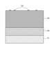
- FIG. 1 is a diagram showing an example of the structure of the semiconductor device according to the embodiment.
- FIG. 2 is a flowchart showing an example of a method for manufacturing a semiconductor device according to an embodiment.
- FIG. 3 is a cross-sectional view showing an example of the state of the object to be processed in each step of the method for manufacturing a semiconductor device according to an embodiment.
- FIG. 4 is a cross-sectional view showing an example of the state of the object to be processed in each step of the method for manufacturing a semiconductor device according to an embodiment.
- FIG. 5 is a cross-sectional view showing an example of the state of the object to be processed in each step of the method for manufacturing a semiconductor device according to an embodiment.
- FIG. 6 is a cross-sectional view showing an example of the state of the object to be processed in each step of the method for manufacturing a semiconductor device according to an embodiment.
- FIG. 7 is a diagram for explaining the details of the metal adhesion step in one embodiment.
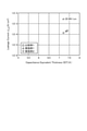
- FIG. 8 is a diagram showing an example of measurement results of CET and leakage current of the dielectric film.
- FIG. 9 is a diagram showing an example of the structure of the semiconductor device according to the modified example of the embodiment.
- the present disclosure provides a technique capable of reducing the leakage current without increasing the CET of the dielectric film.
- FIG. 1 is a diagram showing an example of the structure of a semiconductor device according to an embodiment.
- the semiconductor device 100 shown in FIG. 1 is a semiconductor device having a MIM (Metal-Insulator-Metal) structure.
- the semiconductor device 100 includes a semiconductor substrate 101, a lower electrode 203 formed on the semiconductor substrate 101, a dielectric film 102 formed on the lower electrode 203, and an upper electrode 103 formed on the dielectric film 102.
- the dielectric film 102 is used as a capacitive insulating film between the upper electrode 103 and the lower electrode 203.
- An insulating metal oxide film 104 is locally formed in a predetermined region on the surface of the dielectric film 102.
- FIG. 2 is a flowchart showing an example of a method for manufacturing a semiconductor device according to an embodiment.
- 3 to 6 are cross-sectional views showing an example of the state of the object to be processed in each step of the method for manufacturing a semiconductor device according to an embodiment.
- the semiconductor substrate 101 on which the lower electrode 203 is formed is provided (step S101).
- the semiconductor substrate 101 is, for example, a silicon substrate or the like.
- the lower electrode 203 is, for example, titanium nitride (TiN).
- the dielectric film 102 is formed on the lower electrode 203 (step S102, see FIG. 3).
- the dielectric film 102 contains, for example, hafnium oxide (HfO2) or zirconium oxide (ZrO2).
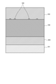
- the metal 104a is selectively attached to a predetermined region on the surface of the dielectric film 102 (step S103, metal attachment step, see FIG. 4).
- the metal 104a contains, for example, aluminum (Al) or a pentavalent transition metal.
- the pentavalent transition metal includes, for example, niobium (Nb) or tantalum (Ta).
- FIG. 7 is a diagram for explaining the details of the metal adhesion step in one embodiment.
- the dielectric film 102 includes a crystallized portion C, which is a crystallized portion, and an amorphous portion ⁇ , which is a non-crystallized portion.
- a crystallized portion C which is a crystallized portion
- amorphous portion ⁇ which is a non-crystallized portion.
- At the grain boundaries, which are the boundary surfaces of the crystal portion C an aggregate in which a plurality of oxygen defect Vos are aggregated is formed. A part of the crystal grain boundaries is exposed on the surface of the dielectric film 102.
- the metal 104a is selectively adhered to the region including the peripheral edge of the crystal grain boundary exposed on the surface of the dielectric film 102 (hereinafter referred to as “grain boundary peripheral region”).
- the metal adhesion step by performing a plating treatment using electrons conducted through the grain boundaries existing in the dielectric film 102 (for example, electrolytic plating treatment), the grain boundary periphery on the surface of the dielectric film 102 is performed.
- Metal 104a is selectively attached to the region. That is, at the crystal grain boundaries existing in the dielectric film 102, a path for conducting electrons from the lower electrode 203 to the surface of the dielectric film 102 is formed by an aggregate of oxygen defects Vo.
- the metal ions in the electrolytic solution are reduced by electrons supplied to the crystal grain boundaries on the surface of the dielectric film 102 by conducting such a path, so that the grain boundaries on the surface of the dielectric film 102 are reduced.
- Metal 104a is selectively attached to the peripheral region.
- an insulating metal oxide film 104 is formed in a predetermined region (that is, a grain boundary peripheral region) on the surface of the dielectric film 102 (step S104, see FIG. 5).
- the metal oxide film 104 is, for example, aluminum oxide (Al2O3), niobium oxide (Nb2O5) or tantalum pentoxide (Ta2O5). From the viewpoint of appropriately growing the metal oxide film 104, the step S104 is preferably performed at a temperature of, for example, 300 ° C. or lower.
- step S104 for example, when the dielectric film 102 is hafnium oxide (HfO2) and the metal oxide film 104 is niobium oxide (Nb2O5), the following chemical reaction formulas (1) and (2) are used. The chemical reaction to proceed proceeds.
- HfO2 hafnium oxide
- Nb2O5 niobium oxide
- Nb2O5 Nb atoms of niobium oxide
- HfO2O4 hafnium oxide
- O atoms of niobium oxide are oxidized. Enter the site of the O atom in the hafnium crystal.
- two electrons and one O atom are left over.
- the surplus two electrons and one O atom enter the oxygen defect Vo at the grain boundary on the surface of the hafnium oxide (dielectric film 102).
- the oxygen defect Vo which is an electron path, disappears near the surface of hafnium oxide (HfO2), and the peripheral edge of the crystal grain boundary on the surface of hafnium oxide is electrically sealed by the metal oxide film 104.
- the leakage current of the dielectric film 102 can be reduced.
- the metal oxide film 104 is tantalum oxide (Ta2O5), and as a result, the leakage current of the dielectric film 102 can be reduced.
- the metal oxide film 104 is aluminum oxide (Al2O3), the covalent bond of the Al—O bond of aluminum oxide is strong and the band gap is large, so that electron tunneling is suppressed, and as a result, the dielectric film 102. Leakage current can be reduced.
- step S104 unlike the conventional technique of forming a metal oxide film on the entire surface of the dielectric film 102 by the ALD method, metal oxidation is selectively performed only on the grain boundary peripheral region on the surface of the dielectric film 102.
- the film 104 is formed. This makes it possible to suppress an increase in the CET of the dielectric film 102.
- the upper electrode 103 is formed on the dielectric film 102 (step S105, see FIG. 6), and the process is completed.
- the upper electrode 103 is, for example, titanium nitride (TiN).
- FIG. 8 is a diagram showing an example of the measurement results of the CET and the leak current of the dielectric film 102.
- FIG. 8 shows the measurement results when the upper electrode 103 of titanium nitride (TiN) is formed on the dielectric film 102 of zirconium oxide (ZrO2).
- Comparative Example 1 of FIG. 8 shows the result of directly forming the upper electrode 103 on the dielectric film 102 without forming the metal oxide film 104.
- the result of forming the upper electrode 103 after forming the metal oxide film 104 is shown.
- the result of forming the upper electrode 103 after forming the metal oxide film 104 is shown.
- the metal oxide film 104 when the metal oxide film 104 is formed, the increase in CET of the dielectric film 102 is suppressed and the leakage current is reduced as compared with the case where the metal oxide film 104 is not formed. That is, according to the method for manufacturing a semiconductor device according to the embodiment in which the metal oxide film 104 is formed in the grain boundary peripheral region on the surface of the dielectric film 102 prior to the formation of the upper electrode 103, the dielectric film 102 is formed. The leakage current can be reduced without increasing the CET. Further, as can be seen from the result of FIG. 8, when the metal oxide film 104 is formed, the CET of the dielectric film 102 is reduced as compared with the case where the metal oxide film 104 is not formed.
- the dielectric film 102 is formed. CET can also be reduced.
- the reason why the CET of the dielectric film 102 is reduced is that the plating treatment forms irregularities based on the oxide of the plated material on the surface of the dielectric film 102 (ZrO2 film), and the effective surface area of the dielectric film 102 is increased. It is considered that the capacity increased with this.
- FIG. 9 is a diagram showing an example of the structure of the semiconductor device 100A according to the modified example of the embodiment.
- the semiconductor device 100A shown in FIG. 9 is a semiconductor device having a MOS structure.
- the semiconductor device 100A has a semiconductor substrate 101, a dielectric film 102 formed on the semiconductor substrate 101, and an upper electrode 103 formed on the dielectric film 102.
- the dielectric film 102 is used as a gate insulating film.
- An insulating metal oxide film 104 is locally formed in a predetermined region (that is, a grain boundary peripheral region) on the surface of the dielectric film 102.
- the upper electrode 103 is used as a gate electrode.
- the method for manufacturing the semiconductor device 100A according to the modified example provides the semiconductor substrate 101 in the step S101 of the embodiment. Further, in the method for manufacturing the semiconductor device 100A, the dielectric film 102 is formed on the semiconductor substrate 101 in the step S102 of one embodiment. In the method for manufacturing the semiconductor device 100A according to the modified example, the processes from the attachment of the metal 104a (step S103) to the formation of the upper electrode 103 (step S105) are the same as those in one embodiment.
- the metal oxide film 104 is formed in the grain boundary peripheral region on the surface of the dielectric film 102 prior to the formation of the upper electrode 103. As a result, the leakage current can be reduced without increasing the CET of the dielectric film 102.
- the method for manufacturing a semiconductor device includes a step of forming a dielectric film on a semiconductor substrate or a lower electrode formed on the semiconductor substrate, and selectively forming a metal in a predetermined region on the surface of the dielectric film.
- the step of forming an upper electrode on the dielectric film is included. Therefore, according to the embodiment, the leakage current can be reduced without increasing the CET of the dielectric film.
- the metal in the step of adhering the metal, the metal may be selectively adhered to the region including the peripheral edge of the crystal grain boundary exposed on the surface of the dielectric film. Therefore, according to the embodiment, it is possible to suppress the generation of leakage current on the surface of the dielectric film.
- the crystal grains exposed on the surface of the dielectric film are subjected to a plating process using electrons conducted through the grain boundaries existing in the dielectric film.
- Metals may be selectively attached to the region including the periphery of the boundary. Therefore, according to the embodiment, the metal can be accurately adhered only to the peripheral edge of the crystal grain boundary exposed on the surface of the dielectric film.
- the metal may contain aluminum (Al) or a pentavalent transition metal.
- the pentavalent transition metal may contain niobium (Nb) or tantalum (Ta).
- the dielectric film may contain hafnium oxide (HfO2) or zirconium oxide (ZrO2). Therefore, according to the embodiment, the leakage current can be reduced without increasing the CET of the dielectric film by using an insulating metal oxide film formed of aluminum (Al) or a pentavalent transition metal. ..
- the step of forming the metal oxide film may be performed at a temperature of 300 ° C. or lower. Therefore, according to the embodiment, the metal oxide film can be appropriately grown on the surface of the dielectric film.
- a step of annealing the metal oxide film under an inert atmosphere is further performed between the step of forming the metal oxide film (step S104) and the step of forming the lower electrode (step S105). It may be included. Further, in this case, the step of annealing the metal oxide film is preferably performed at a temperature of 500 ° C. or lower. As a result, the metal oxide film can be appropriately grown up to the crystal grain boundaries existing in the dielectric film, and as a result, the leakage current can be further reduced.
- the step of annealing the dielectric film under an inert atmosphere is further included between the step of forming the dielectric film (step S102) and the step of adhering the metal (step S103). But it may be. Further, in this case, the step of annealing the dielectric film is preferably performed at a temperature of 500 ° C. or lower. As a result, the dielectric film can be appropriately crystallized.
Landscapes
- Formation Of Insulating Films (AREA)
- Insulated Gate Type Field-Effect Transistor (AREA)
- Semiconductor Integrated Circuits (AREA)
- Semiconductor Memories (AREA)
- Engineering & Computer Science (AREA)
- Manufacturing & Machinery (AREA)
- Power Engineering (AREA)
- Non-Volatile Memory (AREA)
Priority Applications (5)
| Application Number | Priority Date | Filing Date | Title |
|---|---|---|---|
| KR1020237007330A KR102893655B1 (ko) | 2020-09-15 | 2021-09-01 | 반도체 장치의 제조 방법 |
| CN202180061683.XA CN116075924A (zh) | 2020-09-15 | 2021-09-01 | 半导体装置的制造方法 |
| JP2022550446A JP7550868B2 (ja) | 2020-09-15 | 2021-09-01 | 半導体装置の製造方法 |
| KR1020257039751A KR20250174993A (ko) | 2020-09-15 | 2021-09-01 | 반도체 장치의 제조 방법 |
| US18/024,971 US12349434B2 (en) | 2020-09-15 | 2021-09-01 | Manufacturing method for semiconductor device |
Applications Claiming Priority (2)
| Application Number | Priority Date | Filing Date | Title |
|---|---|---|---|
| JP2020154747 | 2020-09-15 | ||
| JP2020-154747 | 2020-09-15 |
Publications (1)
| Publication Number | Publication Date |
|---|---|
| WO2022059482A1 true WO2022059482A1 (ja) | 2022-03-24 |
Family
ID=80775986
Family Applications (1)
| Application Number | Title | Priority Date | Filing Date |
|---|---|---|---|
| PCT/JP2021/032045 Ceased WO2022059482A1 (ja) | 2020-09-15 | 2021-09-01 | 半導体装置の製造方法 |
Country Status (6)
| Country | Link |
|---|---|
| US (1) | US12349434B2 (https=) |
| JP (1) | JP7550868B2 (https=) |
| KR (2) | KR102893655B1 (https=) |
| CN (1) | CN116075924A (https=) |
| TW (1) | TWI906356B (https=) |
| WO (1) | WO2022059482A1 (https=) |
Families Citing this family (1)
| Publication number | Priority date | Publication date | Assignee | Title |
|---|---|---|---|---|
| CN118591281A (zh) * | 2024-08-06 | 2024-09-03 | 武汉新芯集成电路股份有限公司 | 电容器及其制造方法 |
Citations (4)
| Publication number | Priority date | Publication date | Assignee | Title |
|---|---|---|---|---|
| JPS56161669A (en) * | 1980-05-16 | 1981-12-12 | Nec Corp | Manufacture of semiconductor device |
| JP2005079186A (ja) * | 2003-08-28 | 2005-03-24 | Sharp Corp | 微粒子含有体およびその製造方法、メモリ機能体、メモリ素子並びに電子機器 |
| JP2007294874A (ja) * | 2006-03-31 | 2007-11-08 | Sanyo Electric Co Ltd | 半導体装置および半導体装置の製造方法 |
| US20080246078A1 (en) * | 2007-04-03 | 2008-10-09 | Samsung Electronics Co., Ltd. | Charge trap flash memory device and memory card and system including the same |
Family Cites Families (12)
| Publication number | Priority date | Publication date | Assignee | Title |
|---|---|---|---|---|
| JPS56161699A (en) * | 1980-05-16 | 1981-12-12 | Denki Kagaku Kogyo Kk | Method of mounting electric part and insulating heat dissipating sheet used therefor |
| JP3628041B2 (ja) * | 1994-06-29 | 2005-03-09 | テキサス インスツルメンツ インコーポレイテツド | 半導体装置の製造方法 |
| KR100215861B1 (ko) * | 1996-03-13 | 1999-08-16 | 구본준 | 유전체 박막 제조방법 및 이를 이용한 반도체 장치제조방법 |
| KR100252055B1 (ko) * | 1997-12-11 | 2000-04-15 | 윤종용 | 커패시터를 포함하는 반도체장치 및 그 제조방법 |
| US20050142715A1 (en) * | 2003-12-26 | 2005-06-30 | Fujitsu Limited | Semiconductor device with high dielectric constant insulator and its manufacture |
| JP4909552B2 (ja) * | 2005-09-12 | 2012-04-04 | 旭硝子株式会社 | 電荷保持特性に優れた不揮発性半導体記憶素子の製造方法 |
| JP2007088301A (ja) | 2005-09-22 | 2007-04-05 | Toshiba Corp | 半導体装置および半導体装置の製造方法 |
| US20120064690A1 (en) | 2010-09-10 | 2012-03-15 | Elpida Memory, Inc. | Method for manufacturing semiconductor device |
| JP2014229680A (ja) * | 2013-05-21 | 2014-12-08 | ピーエスフォー ルクスコ エスエイアールエルPS4 Luxco S.a.r.l. | 半導体装置及びその製造方法 |
| US9275853B2 (en) * | 2013-07-29 | 2016-03-01 | Applied Materials, Inc. | Method of adjusting a transistor gate flat band voltage with addition of AL203 on nitrided silicon channel |
| KR102470206B1 (ko) * | 2017-10-13 | 2022-11-23 | 삼성디스플레이 주식회사 | 금속 산화막의 제조 방법 및 금속 산화막을 포함하는 표시 소자 |
| JP2024161669A (ja) | 2023-05-08 | 2024-11-20 | 三菱電機株式会社 | Pio装置およびpio装置の寿命判定方法 |
-
2021
- 2021-09-01 KR KR1020237007330A patent/KR102893655B1/ko active Active
- 2021-09-01 US US18/024,971 patent/US12349434B2/en active Active
- 2021-09-01 CN CN202180061683.XA patent/CN116075924A/zh active Pending
- 2021-09-01 TW TW110132417A patent/TWI906356B/zh active
- 2021-09-01 KR KR1020257039751A patent/KR20250174993A/ko active Pending
- 2021-09-01 WO PCT/JP2021/032045 patent/WO2022059482A1/ja not_active Ceased
- 2021-09-01 JP JP2022550446A patent/JP7550868B2/ja active Active
Patent Citations (4)
| Publication number | Priority date | Publication date | Assignee | Title |
|---|---|---|---|---|
| JPS56161669A (en) * | 1980-05-16 | 1981-12-12 | Nec Corp | Manufacture of semiconductor device |
| JP2005079186A (ja) * | 2003-08-28 | 2005-03-24 | Sharp Corp | 微粒子含有体およびその製造方法、メモリ機能体、メモリ素子並びに電子機器 |
| JP2007294874A (ja) * | 2006-03-31 | 2007-11-08 | Sanyo Electric Co Ltd | 半導体装置および半導体装置の製造方法 |
| US20080246078A1 (en) * | 2007-04-03 | 2008-10-09 | Samsung Electronics Co., Ltd. | Charge trap flash memory device and memory card and system including the same |
Also Published As
| Publication number | Publication date |
|---|---|
| JPWO2022059482A1 (https=) | 2022-03-24 |
| US20230326977A1 (en) | 2023-10-12 |
| JP7550868B2 (ja) | 2024-09-13 |
| KR20250174993A (ko) | 2025-12-15 |
| KR20230066333A (ko) | 2023-05-15 |
| CN116075924A (zh) | 2023-05-05 |
| TW202223988A (zh) | 2022-06-16 |
| KR102893655B1 (ko) | 2025-12-01 |
| US12349434B2 (en) | 2025-07-01 |
| TWI906356B (zh) | 2025-12-01 |
Similar Documents
| Publication | Publication Date | Title |
|---|---|---|
| JP2009194351A (ja) | 薄膜トランジスタおよびその製造方法 | |
| JP2001267566A (ja) | 多層誘電体スタックおよびその方法 | |
| US8649154B2 (en) | Method for producing a metal-insulator-metal capacitor for use in semiconductor devices | |
| US6849908B2 (en) | Semiconductor device and method of manufacturing the same | |
| JP2001015739A (ja) | ゲート絶縁膜とその製造方法 | |
| KR102045027B1 (ko) | 산화물 박막 트랜지스터 제조 방법 및 이를 이용해서 제조되는 산화물 박막 트랜지스터 | |
| JP5458514B2 (ja) | 半導体装置の製造方法、及び半導体装置 | |
| TWI233648B (en) | Semiconductor device fabrication method | |
| WO2022059482A1 (ja) | 半導体装置の製造方法 | |
| CN106252203B (zh) | 金属氧化物半导体层的结晶方法及半导体结构 | |
| TWI779254B (zh) | 薄膜電晶體的製造方法 | |
| JP5685125B2 (ja) | 配線構造、表示装置、および半導体装置 | |
| TWI611483B (zh) | 薄膜電晶體製造方法及薄膜電晶體 | |
| JP5197986B2 (ja) | 半導体装置の製造装置 | |
| TW202009975A (zh) | 藉由氮化鈦與鋁膜的整合沉積用於摻雜工程與臨界電壓調整之方法與設備 | |
| US12604537B2 (en) | High mobility transistor element resulting from IGTO oxide semiconductor crystallization, and production method for same | |
| TWI777179B (zh) | 閘極介電層的製作方法 | |
| TW202107538A (zh) | 用於改良高k可靠度之摻氟氮化物膜 | |
| JP2005079563A (ja) | 電子デバイスの製造方法 | |
| KR20020034710A (ko) | 하프늄 산화막과 전도층의 반응을 억제할 수 있는 반도체장치 제조 방법 | |
| TWI609415B (zh) | 半導體裝置電極的製造方法 | |
| JP2024051448A (ja) | 半導体装置の製造方法および半導体装置 | |
| KR101078716B1 (ko) | 반도체 소자의 게이트 형성방법 | |
| JP2006229044A (ja) | 半導体装置 | |
| TW202445868A (zh) | 薄膜電晶體的鈍化元件 |
Legal Events
| Date | Code | Title | Description |
|---|---|---|---|
| 121 | Ep: the epo has been informed by wipo that ep was designated in this application |
Ref document number: 21869169 Country of ref document: EP Kind code of ref document: A1 |
|
| ENP | Entry into the national phase |
Ref document number: 2022550446 Country of ref document: JP Kind code of ref document: A |
|
| NENP | Non-entry into the national phase |
Ref country code: DE |
|
| 122 | Ep: pct application non-entry in european phase |
Ref document number: 21869169 Country of ref document: EP Kind code of ref document: A1 |
|
| WWG | Wipo information: grant in national office |
Ref document number: 18024971 Country of ref document: US |