WO2022029541A1 - 半導体装置 - Google Patents
半導体装置 Download PDFInfo
- Publication number
- WO2022029541A1 WO2022029541A1 PCT/IB2021/056692 IB2021056692W WO2022029541A1 WO 2022029541 A1 WO2022029541 A1 WO 2022029541A1 IB 2021056692 W IB2021056692 W IB 2021056692W WO 2022029541 A1 WO2022029541 A1 WO 2022029541A1
- Authority
- WO
- WIPO (PCT)
- Prior art keywords
- insulator
- transistor
- oxide
- conductor
- circuit
- Prior art date
Links
- 239000004065 semiconductor Substances 0.000 title claims abstract description 412
- 230000006870 function Effects 0.000 claims abstract description 182
- 229910052710 silicon Inorganic materials 0.000 claims description 50
- 239000010703 silicon Substances 0.000 claims description 50
- 238000010168 coupling process Methods 0.000 claims description 5
- 238000005859 coupling reaction Methods 0.000 claims description 5
- 230000015572 biosynthetic process Effects 0.000 abstract description 17
- 239000012212 insulator Substances 0.000 description 644
- 239000004020 conductor Substances 0.000 description 355
- 239000010408 film Substances 0.000 description 127
- 239000010410 layer Substances 0.000 description 120
- 229910052760 oxygen Inorganic materials 0.000 description 111
- 239000001301 oxygen Substances 0.000 description 111
- QVGXLLKOCUKJST-UHFFFAOYSA-N atomic oxygen Chemical compound [O] QVGXLLKOCUKJST-UHFFFAOYSA-N 0.000 description 109
- 239000001257 hydrogen Substances 0.000 description 106
- 229910052739 hydrogen Inorganic materials 0.000 description 106
- UFHFLCQGNIYNRP-UHFFFAOYSA-N Hydrogen Chemical compound [H][H] UFHFLCQGNIYNRP-UHFFFAOYSA-N 0.000 description 96
- 238000012545 processing Methods 0.000 description 74
- 239000000758 substrate Substances 0.000 description 68
- 239000012535 impurity Substances 0.000 description 66
- 239000000463 material Substances 0.000 description 63
- 238000000034 method Methods 0.000 description 62
- 239000013078 crystal Substances 0.000 description 56
- 229910044991 metal oxide Inorganic materials 0.000 description 55
- 150000004706 metal oxides Chemical class 0.000 description 55
- 238000004364 calculation method Methods 0.000 description 53
- XUIMIQQOPSSXEZ-UHFFFAOYSA-N Silicon Chemical compound [Si] XUIMIQQOPSSXEZ-UHFFFAOYSA-N 0.000 description 49
- 230000004888 barrier function Effects 0.000 description 43
- 238000010586 diagram Methods 0.000 description 39
- IJGRMHOSHXDMSA-UHFFFAOYSA-N Atomic nitrogen Chemical compound N#N IJGRMHOSHXDMSA-UHFFFAOYSA-N 0.000 description 38
- 239000011701 zinc Substances 0.000 description 37
- 229910052581 Si3N4 Inorganic materials 0.000 description 33
- 238000009792 diffusion process Methods 0.000 description 33
- 229910052814 silicon oxide Inorganic materials 0.000 description 31
- VYPSYNLAJGMNEJ-UHFFFAOYSA-N silicon dioxide Inorganic materials O=[Si]=O VYPSYNLAJGMNEJ-UHFFFAOYSA-N 0.000 description 30
- TWNQGVIAIRXVLR-UHFFFAOYSA-N oxo(oxoalumanyloxy)alumane Chemical compound O=[Al]O[Al]=O TWNQGVIAIRXVLR-UHFFFAOYSA-N 0.000 description 29
- HQVNEWCFYHHQES-UHFFFAOYSA-N silicon nitride Chemical compound N12[Si]34N5[Si]62N3[Si]51N64 HQVNEWCFYHHQES-UHFFFAOYSA-N 0.000 description 29
- 238000013473 artificial intelligence Methods 0.000 description 28
- 229910052735 hafnium Inorganic materials 0.000 description 28
- 229910052782 aluminium Inorganic materials 0.000 description 27
- XAGFODPZIPBFFR-UHFFFAOYSA-N aluminium Chemical compound [Al] XAGFODPZIPBFFR-UHFFFAOYSA-N 0.000 description 27
- 210000004027 cell Anatomy 0.000 description 27
- 229910001868 water Inorganic materials 0.000 description 27
- 230000008569 process Effects 0.000 description 26
- XLYOFNOQVPJJNP-UHFFFAOYSA-N water Substances O XLYOFNOQVPJJNP-UHFFFAOYSA-N 0.000 description 26
- VBJZVLUMGGDVMO-UHFFFAOYSA-N hafnium atom Chemical compound [Hf] VBJZVLUMGGDVMO-UHFFFAOYSA-N 0.000 description 22
- 125000004429 atom Chemical group 0.000 description 21
- -1 ittrium Chemical compound 0.000 description 21
- 229910052721 tungsten Inorganic materials 0.000 description 21
- 239000010937 tungsten Substances 0.000 description 21
- WFKWXMTUELFFGS-UHFFFAOYSA-N tungsten Chemical compound [W] WFKWXMTUELFFGS-UHFFFAOYSA-N 0.000 description 20
- 229910052757 nitrogen Inorganic materials 0.000 description 19
- 206010021143 Hypoxia Diseases 0.000 description 18
- 238000000707 layer-by-layer assembly Methods 0.000 description 18
- 239000000203 mixture Substances 0.000 description 18
- 230000007547 defect Effects 0.000 description 17
- 229910052751 metal Inorganic materials 0.000 description 17
- 230000003071 parasitic effect Effects 0.000 description 17
- 238000003860 storage Methods 0.000 description 17
- 238000010438 heat treatment Methods 0.000 description 15
- 150000004767 nitrides Chemical class 0.000 description 15
- 239000002356 single layer Substances 0.000 description 15
- 229910000449 hafnium oxide Inorganic materials 0.000 description 14
- WIHZLLGSGQNAGK-UHFFFAOYSA-N hafnium(4+);oxygen(2-) Chemical compound [O-2].[O-2].[Hf+4] WIHZLLGSGQNAGK-UHFFFAOYSA-N 0.000 description 14
- 150000002431 hydrogen Chemical class 0.000 description 14
- RYGMFSIKBFXOCR-UHFFFAOYSA-N Copper Chemical compound [Cu] RYGMFSIKBFXOCR-UHFFFAOYSA-N 0.000 description 13
- RTAQQCXQSZGOHL-UHFFFAOYSA-N Titanium Chemical compound [Ti] RTAQQCXQSZGOHL-UHFFFAOYSA-N 0.000 description 13
- 229910052738 indium Inorganic materials 0.000 description 13
- 239000002184 metal Substances 0.000 description 13
- 229910052719 titanium Inorganic materials 0.000 description 13
- 239000010936 titanium Substances 0.000 description 13
- PXHVJJICTQNCMI-UHFFFAOYSA-N Nickel Chemical compound [Ni] PXHVJJICTQNCMI-UHFFFAOYSA-N 0.000 description 12
- 238000000231 atomic layer deposition Methods 0.000 description 12
- 230000007812 deficiency Effects 0.000 description 12
- 230000005669 field effect Effects 0.000 description 12
- 238000004519 manufacturing process Methods 0.000 description 12
- 229910052715 tantalum Inorganic materials 0.000 description 12
- GUVRBAGPIYLISA-UHFFFAOYSA-N tantalum atom Chemical compound [Ta] GUVRBAGPIYLISA-UHFFFAOYSA-N 0.000 description 12
- 230000008859 change Effects 0.000 description 11
- 239000010949 copper Substances 0.000 description 11
- 230000000694 effects Effects 0.000 description 11
- 229910052733 gallium Inorganic materials 0.000 description 11
- APFVFJFRJDLVQX-UHFFFAOYSA-N indium atom Chemical compound [In] APFVFJFRJDLVQX-UHFFFAOYSA-N 0.000 description 11
- OKTJSMMVPCPJKN-UHFFFAOYSA-N Carbon Chemical compound [C] OKTJSMMVPCPJKN-UHFFFAOYSA-N 0.000 description 10
- XEEYBQQBJWHFJM-UHFFFAOYSA-N Iron Chemical compound [Fe] XEEYBQQBJWHFJM-UHFFFAOYSA-N 0.000 description 10
- 229910052802 copper Inorganic materials 0.000 description 10
- 230000020169 heat generation Effects 0.000 description 10
- GYHNNYVSQQEPJS-UHFFFAOYSA-N Gallium Chemical compound [Ga] GYHNNYVSQQEPJS-UHFFFAOYSA-N 0.000 description 9
- MWUXSHHQAYIFBG-UHFFFAOYSA-N Nitric oxide Chemical compound O=[N] MWUXSHHQAYIFBG-UHFFFAOYSA-N 0.000 description 9
- 238000013528 artificial neural network Methods 0.000 description 9
- 229910052799 carbon Inorganic materials 0.000 description 9
- 239000000969 carrier Substances 0.000 description 9
- ZOKXTWBITQBERF-UHFFFAOYSA-N Molybdenum Chemical compound [Mo] ZOKXTWBITQBERF-UHFFFAOYSA-N 0.000 description 8
- NRTOMJZYCJJWKI-UHFFFAOYSA-N Titanium nitride Chemical compound [Ti]#N NRTOMJZYCJJWKI-UHFFFAOYSA-N 0.000 description 8
- 238000013527 convolutional neural network Methods 0.000 description 8
- 239000012528 membrane Substances 0.000 description 8
- 229910052750 molybdenum Inorganic materials 0.000 description 8
- 239000011733 molybdenum Substances 0.000 description 8
- MZLGASXMSKOWSE-UHFFFAOYSA-N tantalum nitride Chemical compound [Ta]#N MZLGASXMSKOWSE-UHFFFAOYSA-N 0.000 description 8
- 229910052725 zinc Inorganic materials 0.000 description 8
- 230000005684 electric field Effects 0.000 description 7
- 239000011229 interlayer Substances 0.000 description 7
- 229910052746 lanthanum Inorganic materials 0.000 description 7
- 239000002159 nanocrystal Substances 0.000 description 7
- 125000004430 oxygen atom Chemical group O* 0.000 description 7
- 238000001004 secondary ion mass spectrometry Methods 0.000 description 7
- 238000001228 spectrum Methods 0.000 description 7
- 238000004544 sputter deposition Methods 0.000 description 7
- 239000000126 substance Substances 0.000 description 7
- 229910052727 yttrium Inorganic materials 0.000 description 7
- ZOXJGFHDIHLPTG-UHFFFAOYSA-N Boron Chemical compound [B] ZOXJGFHDIHLPTG-UHFFFAOYSA-N 0.000 description 6
- MYMOFIZGZYHOMD-UHFFFAOYSA-N Dioxygen Chemical compound O=O MYMOFIZGZYHOMD-UHFFFAOYSA-N 0.000 description 6
- 229910052779 Neodymium Inorganic materials 0.000 description 6
- HCHKCACWOHOZIP-UHFFFAOYSA-N Zinc Chemical compound [Zn] HCHKCACWOHOZIP-UHFFFAOYSA-N 0.000 description 6
- 229910052796 boron Inorganic materials 0.000 description 6
- 238000005516 engineering process Methods 0.000 description 6
- 229910003437 indium oxide Inorganic materials 0.000 description 6
- PJXISJQVUVHSOJ-UHFFFAOYSA-N indium(iii) oxide Chemical compound [O-2].[O-2].[O-2].[In+3].[In+3] PJXISJQVUVHSOJ-UHFFFAOYSA-N 0.000 description 6
- FZLIPJUXYLNCLC-UHFFFAOYSA-N lanthanum atom Chemical compound [La] FZLIPJUXYLNCLC-UHFFFAOYSA-N 0.000 description 6
- 229910052451 lead zirconate titanate Inorganic materials 0.000 description 6
- CPLXHLVBOLITMK-UHFFFAOYSA-N magnesium oxide Inorganic materials [Mg]=O CPLXHLVBOLITMK-UHFFFAOYSA-N 0.000 description 6
- 229910052759 nickel Inorganic materials 0.000 description 6
- 239000000047 product Substances 0.000 description 6
- 229910052718 tin Inorganic materials 0.000 description 6
- VWQVUPCCIRVNHF-UHFFFAOYSA-N yttrium atom Chemical group [Y] VWQVUPCCIRVNHF-UHFFFAOYSA-N 0.000 description 6
- 229910052726 zirconium Inorganic materials 0.000 description 6
- 102100036285 25-hydroxyvitamin D-1 alpha hydroxylase, mitochondrial Human genes 0.000 description 5
- 229910052684 Cerium Inorganic materials 0.000 description 5
- 101000875403 Homo sapiens 25-hydroxyvitamin D-1 alpha hydroxylase, mitochondrial Proteins 0.000 description 5
- ATJFFYVFTNAWJD-UHFFFAOYSA-N Tin Chemical group [Sn] ATJFFYVFTNAWJD-UHFFFAOYSA-N 0.000 description 5
- QCWXUUIWCKQGHC-UHFFFAOYSA-N Zirconium Chemical compound [Zr] QCWXUUIWCKQGHC-UHFFFAOYSA-N 0.000 description 5
- 238000005229 chemical vapour deposition Methods 0.000 description 5
- PMHQVHHXPFUNSP-UHFFFAOYSA-M copper(1+);methylsulfanylmethane;bromide Chemical compound Br[Cu].CSC PMHQVHHXPFUNSP-UHFFFAOYSA-M 0.000 description 5
- 238000010894 electron beam technology Methods 0.000 description 5
- 238000002003 electron diffraction Methods 0.000 description 5
- 229910052732 germanium Inorganic materials 0.000 description 5
- GNPVGFCGXDBREM-UHFFFAOYSA-N germanium atom Chemical compound [Ge] GNPVGFCGXDBREM-UHFFFAOYSA-N 0.000 description 5
- 125000004435 hydrogen atom Chemical group [H]* 0.000 description 5
- 229910052742 iron Inorganic materials 0.000 description 5
- 239000000395 magnesium oxide Substances 0.000 description 5
- 239000011159 matrix material Substances 0.000 description 5
- 239000007769 metal material Substances 0.000 description 5
- QEFYFXOXNSNQGX-UHFFFAOYSA-N neodymium atom Chemical compound [Nd] QEFYFXOXNSNQGX-UHFFFAOYSA-N 0.000 description 5
- 230000003647 oxidation Effects 0.000 description 5
- 238000007254 oxidation reaction Methods 0.000 description 5
- 230000002093 peripheral effect Effects 0.000 description 5
- 230000009467 reduction Effects 0.000 description 5
- 229910052707 ruthenium Inorganic materials 0.000 description 5
- 238000000926 separation method Methods 0.000 description 5
- 229910052712 strontium Inorganic materials 0.000 description 5
- 239000010409 thin film Substances 0.000 description 5
- OGIDPMRJRNCKJF-UHFFFAOYSA-N titanium oxide Inorganic materials [Ti]=O OGIDPMRJRNCKJF-UHFFFAOYSA-N 0.000 description 5
- JBRZTFJDHDCESZ-UHFFFAOYSA-N AsGa Chemical compound [As]#[Ga] JBRZTFJDHDCESZ-UHFFFAOYSA-N 0.000 description 4
- 229910001218 Gallium arsenide Inorganic materials 0.000 description 4
- 101001056180 Homo sapiens Induced myeloid leukemia cell differentiation protein Mcl-1 Proteins 0.000 description 4
- 102100026539 Induced myeloid leukemia cell differentiation protein Mcl-1 Human genes 0.000 description 4
- FYYHWMGAXLPEAU-UHFFFAOYSA-N Magnesium Chemical compound [Mg] FYYHWMGAXLPEAU-UHFFFAOYSA-N 0.000 description 4
- KJTLSVCANCCWHF-UHFFFAOYSA-N Ruthenium Chemical compound [Ru] KJTLSVCANCCWHF-UHFFFAOYSA-N 0.000 description 4
- 101150075681 SCL1 gene Proteins 0.000 description 4
- XLOMVQKBTHCTTD-UHFFFAOYSA-N Zinc monoxide Chemical compound [Zn]=O XLOMVQKBTHCTTD-UHFFFAOYSA-N 0.000 description 4
- 229910052783 alkali metal Inorganic materials 0.000 description 4
- 150000001340 alkali metals Chemical class 0.000 description 4
- 229910052784 alkaline earth metal Inorganic materials 0.000 description 4
- 150000001342 alkaline earth metals Chemical class 0.000 description 4
- 230000005540 biological transmission Effects 0.000 description 4
- ZMIGMASIKSOYAM-UHFFFAOYSA-N cerium Chemical compound [Ce][Ce][Ce][Ce][Ce][Ce][Ce][Ce][Ce][Ce][Ce][Ce][Ce][Ce][Ce][Ce][Ce][Ce][Ce][Ce][Ce][Ce][Ce][Ce][Ce][Ce][Ce][Ce][Ce][Ce][Ce][Ce][Ce][Ce][Ce][Ce][Ce][Ce] ZMIGMASIKSOYAM-UHFFFAOYSA-N 0.000 description 4
- 238000006243 chemical reaction Methods 0.000 description 4
- 238000012937 correction Methods 0.000 description 4
- AJNVQOSZGJRYEI-UHFFFAOYSA-N digallium;oxygen(2-) Chemical compound [O-2].[O-2].[O-2].[Ga+3].[Ga+3] AJNVQOSZGJRYEI-UHFFFAOYSA-N 0.000 description 4
- 238000002149 energy-dispersive X-ray emission spectroscopy Methods 0.000 description 4
- 229910001195 gallium oxide Inorganic materials 0.000 description 4
- 239000007789 gas Substances 0.000 description 4
- 239000011521 glass Substances 0.000 description 4
- 239000011810 insulating material Substances 0.000 description 4
- 229910052749 magnesium Inorganic materials 0.000 description 4
- 239000011777 magnesium Substances 0.000 description 4
- AXZKOIWUVFPNLO-UHFFFAOYSA-N magnesium;oxygen(2-) Chemical compound [O-2].[Mg+2] AXZKOIWUVFPNLO-UHFFFAOYSA-N 0.000 description 4
- 101150035574 mcl2 gene Proteins 0.000 description 4
- 238000005259 measurement Methods 0.000 description 4
- BPUBBGLMJRNUCC-UHFFFAOYSA-N oxygen(2-);tantalum(5+) Chemical compound [O-2].[O-2].[O-2].[O-2].[O-2].[Ta+5].[Ta+5] BPUBBGLMJRNUCC-UHFFFAOYSA-N 0.000 description 4
- RVTZCBVAJQQJTK-UHFFFAOYSA-N oxygen(2-);zirconium(4+) Chemical compound [O-2].[O-2].[Zr+4] RVTZCBVAJQQJTK-UHFFFAOYSA-N 0.000 description 4
- 239000012466 permeate Substances 0.000 description 4
- 238000011176 pooling Methods 0.000 description 4
- 229910001925 ruthenium oxide Inorganic materials 0.000 description 4
- WOCIAKWEIIZHES-UHFFFAOYSA-N ruthenium(iv) oxide Chemical compound O=[Ru]=O WOCIAKWEIIZHES-UHFFFAOYSA-N 0.000 description 4
- 239000000523 sample Substances 0.000 description 4
- 229920006395 saturated elastomer Polymers 0.000 description 4
- 229910001936 tantalum oxide Inorganic materials 0.000 description 4
- 229910001928 zirconium oxide Inorganic materials 0.000 description 4
- 229910002601 GaN Inorganic materials 0.000 description 3
- JMASRVWKEDWRBT-UHFFFAOYSA-N Gallium nitride Chemical compound [Ga]#N JMASRVWKEDWRBT-UHFFFAOYSA-N 0.000 description 3
- 229910000577 Silicon-germanium Inorganic materials 0.000 description 3
- GWEVSGVZZGPLCZ-UHFFFAOYSA-N Titan oxide Chemical compound O=[Ti]=O GWEVSGVZZGPLCZ-UHFFFAOYSA-N 0.000 description 3
- 238000004833 X-ray photoelectron spectroscopy Methods 0.000 description 3
- 230000009471 action Effects 0.000 description 3
- 239000000956 alloy Substances 0.000 description 3
- 229910052788 barium Inorganic materials 0.000 description 3
- 230000015556 catabolic process Effects 0.000 description 3
- 238000005520 cutting process Methods 0.000 description 3
- 238000013461 design Methods 0.000 description 3
- 229910001873 dinitrogen Inorganic materials 0.000 description 3
- 238000007599 discharging Methods 0.000 description 3
- AMGQUBHHOARCQH-UHFFFAOYSA-N indium;oxotin Chemical compound [In].[Sn]=O AMGQUBHHOARCQH-UHFFFAOYSA-N 0.000 description 3
- 239000011261 inert gas Substances 0.000 description 3
- 230000010354 integration Effects 0.000 description 3
- HFGPZNIAWCZYJU-UHFFFAOYSA-N lead zirconate titanate Chemical compound [O-2].[O-2].[O-2].[O-2].[O-2].[Ti+4].[Zr+4].[Pb+2] HFGPZNIAWCZYJU-UHFFFAOYSA-N 0.000 description 3
- 125000004433 nitrogen atom Chemical group N* 0.000 description 3
- QGLKJKCYBOYXKC-UHFFFAOYSA-N nonaoxidotritungsten Chemical compound O=[W]1(=O)O[W](=O)(=O)O[W](=O)(=O)O1 QGLKJKCYBOYXKC-UHFFFAOYSA-N 0.000 description 3
- 230000001590 oxidative effect Effects 0.000 description 3
- 238000003909 pattern recognition Methods 0.000 description 3
- 239000004033 plastic Substances 0.000 description 3
- 229920003023 plastic Polymers 0.000 description 3
- CIOAGBVUUVVLOB-UHFFFAOYSA-N strontium atom Chemical compound [Sr] CIOAGBVUUVVLOB-UHFFFAOYSA-N 0.000 description 3
- 229910001930 tungsten oxide Inorganic materials 0.000 description 3
- 229910052720 vanadium Inorganic materials 0.000 description 3
- GPPXJZIENCGNKB-UHFFFAOYSA-N vanadium Chemical compound [V]#[V] GPPXJZIENCGNKB-UHFFFAOYSA-N 0.000 description 3
- YVTHLONGBIQYBO-UHFFFAOYSA-N zinc indium(3+) oxygen(2-) Chemical compound [O--].[Zn++].[In+3] YVTHLONGBIQYBO-UHFFFAOYSA-N 0.000 description 3
- 101100059544 Arabidopsis thaliana CDC5 gene Proteins 0.000 description 2
- 101100244969 Arabidopsis thaliana PRL1 gene Proteins 0.000 description 2
- PXGOKWXKJXAPGV-UHFFFAOYSA-N Fluorine Chemical compound FF PXGOKWXKJXAPGV-UHFFFAOYSA-N 0.000 description 2
- 102100039558 Galectin-3 Human genes 0.000 description 2
- 101100454448 Homo sapiens LGALS3 gene Proteins 0.000 description 2
- 101150115300 MAC1 gene Proteins 0.000 description 2
- 101150051246 MAC2 gene Proteins 0.000 description 2
- GQPLMRYTRLFLPF-UHFFFAOYSA-N Nitrous Oxide Chemical compound [O-][N+]#N GQPLMRYTRLFLPF-UHFFFAOYSA-N 0.000 description 2
- BPQQTUXANYXVAA-UHFFFAOYSA-N Orthosilicate Chemical compound [O-][Si]([O-])([O-])[O-] BPQQTUXANYXVAA-UHFFFAOYSA-N 0.000 description 2
- OAICVXFJPJFONN-UHFFFAOYSA-N Phosphorus Chemical compound [P] OAICVXFJPJFONN-UHFFFAOYSA-N 0.000 description 2
- 238000002441 X-ray diffraction Methods 0.000 description 2
- 229910021417 amorphous silicon Inorganic materials 0.000 description 2
- 238000004458 analytical method Methods 0.000 description 2
- 229910052785 arsenic Inorganic materials 0.000 description 2
- RQNWIZPPADIBDY-UHFFFAOYSA-N arsenic atom Chemical compound [As] RQNWIZPPADIBDY-UHFFFAOYSA-N 0.000 description 2
- 239000002585 base Substances 0.000 description 2
- 230000006399 behavior Effects 0.000 description 2
- 229910052790 beryllium Inorganic materials 0.000 description 2
- ATBAMAFKBVZNFJ-UHFFFAOYSA-N beryllium atom Chemical compound [Be] ATBAMAFKBVZNFJ-UHFFFAOYSA-N 0.000 description 2
- 230000000903 blocking effect Effects 0.000 description 2
- 239000000919 ceramic Substances 0.000 description 2
- 150000001875 compounds Chemical class 0.000 description 2
- 238000001816 cooling Methods 0.000 description 2
- 230000008878 coupling Effects 0.000 description 2
- 238000003795 desorption Methods 0.000 description 2
- 230000001066 destructive effect Effects 0.000 description 2
- 230000006866 deterioration Effects 0.000 description 2
- 238000002524 electron diffraction data Methods 0.000 description 2
- 239000011737 fluorine Substances 0.000 description 2
- 229910052731 fluorine Inorganic materials 0.000 description 2
- 239000011888 foil Substances 0.000 description 2
- 230000014509 gene expression Effects 0.000 description 2
- 230000006266 hibernation Effects 0.000 description 2
- 150000002500 ions Chemical class 0.000 description 2
- 238000010030 laminating Methods 0.000 description 2
- 238000002156 mixing Methods 0.000 description 2
- 238000010606 normalization Methods 0.000 description 2
- 229910052698 phosphorus Inorganic materials 0.000 description 2
- 239000011574 phosphorus Substances 0.000 description 2
- 230000000704 physical effect Effects 0.000 description 2
- 229920000139 polyethylene terephthalate Polymers 0.000 description 2
- 239000005020 polyethylene terephthalate Substances 0.000 description 2
- 229920001343 polytetrafluoroethylene Polymers 0.000 description 2
- 239000004810 polytetrafluoroethylene Substances 0.000 description 2
- 239000011148 porous material Substances 0.000 description 2
- 239000002243 precursor Substances 0.000 description 2
- 238000004549 pulsed laser deposition Methods 0.000 description 2
- 230000006798 recombination Effects 0.000 description 2
- 238000005215 recombination Methods 0.000 description 2
- 239000011819 refractory material Substances 0.000 description 2
- 230000003252 repetitive effect Effects 0.000 description 2
- 229920005989 resin Polymers 0.000 description 2
- 239000011347 resin Substances 0.000 description 2
- 230000004044 response Effects 0.000 description 2
- 229910000679 solder Inorganic materials 0.000 description 2
- 239000010935 stainless steel Substances 0.000 description 2
- 229910001220 stainless steel Inorganic materials 0.000 description 2
- 230000003068 static effect Effects 0.000 description 2
- VEALVRVVWBQVSL-UHFFFAOYSA-N strontium titanate Chemical compound [Sr+2].[O-][Ti]([O-])=O VEALVRVVWBQVSL-UHFFFAOYSA-N 0.000 description 2
- 238000012916 structural analysis Methods 0.000 description 2
- 239000013589 supplement Substances 0.000 description 2
- 238000012360 testing method Methods 0.000 description 2
- 238000012546 transfer Methods 0.000 description 2
- 238000005406 washing Methods 0.000 description 2
- 239000011787 zinc oxide Substances 0.000 description 2
- 210000002925 A-like Anatomy 0.000 description 1
- 102100027992 Casein kinase II subunit beta Human genes 0.000 description 1
- VYZAMTAEIAYCRO-UHFFFAOYSA-N Chromium Chemical compound [Cr] VYZAMTAEIAYCRO-UHFFFAOYSA-N 0.000 description 1
- 239000004593 Epoxy Substances 0.000 description 1
- 229910052688 Gadolinium Inorganic materials 0.000 description 1
- 235000015842 Hesperis Nutrition 0.000 description 1
- 101000858625 Homo sapiens Casein kinase II subunit beta Proteins 0.000 description 1
- 235000012633 Iberis amara Nutrition 0.000 description 1
- GPXJNWSHGFTCBW-UHFFFAOYSA-N Indium phosphide Chemical compound [In]#P GPXJNWSHGFTCBW-UHFFFAOYSA-N 0.000 description 1
- 241001465754 Metazoa Species 0.000 description 1
- 235000007164 Oryza sativa Nutrition 0.000 description 1
- 240000007594 Oryza sativa Species 0.000 description 1
- 229920012266 Poly(ether sulfone) PES Polymers 0.000 description 1
- 239000004952 Polyamide Substances 0.000 description 1
- 239000004642 Polyimide Substances 0.000 description 1
- 239000004743 Polypropylene Substances 0.000 description 1
- 229910007610 Zn—Sn Inorganic materials 0.000 description 1
- LEVVHYCKPQWKOP-UHFFFAOYSA-N [Si].[Ge] Chemical compound [Si].[Ge] LEVVHYCKPQWKOP-UHFFFAOYSA-N 0.000 description 1
- NIXOWILDQLNWCW-UHFFFAOYSA-N acrylic acid group Chemical group C(C=C)(=O)O NIXOWILDQLNWCW-UHFFFAOYSA-N 0.000 description 1
- 230000004913 activation Effects 0.000 description 1
- 229910045601 alloy Inorganic materials 0.000 description 1
- MDPILPRLPQYEEN-UHFFFAOYSA-N aluminium arsenide Chemical compound [As]#[Al] MDPILPRLPQYEEN-UHFFFAOYSA-N 0.000 description 1
- 239000005407 aluminoborosilicate glass Substances 0.000 description 1
- 239000004760 aramid Substances 0.000 description 1
- 229920003235 aromatic polyamide Polymers 0.000 description 1
- GPBUGPUPKAGMDK-UHFFFAOYSA-N azanylidynemolybdenum Chemical compound [Mo]#N GPBUGPUPKAGMDK-UHFFFAOYSA-N 0.000 description 1
- DSAJWYNOEDNPEQ-UHFFFAOYSA-N barium atom Chemical compound [Ba] DSAJWYNOEDNPEQ-UHFFFAOYSA-N 0.000 description 1
- JRPBQTZRNDNNOP-UHFFFAOYSA-N barium titanate Chemical compound [Ba+2].[Ba+2].[O-][Ti]([O-])([O-])[O-] JRPBQTZRNDNNOP-UHFFFAOYSA-N 0.000 description 1
- 229910002113 barium titanate Inorganic materials 0.000 description 1
- 230000008901 benefit Effects 0.000 description 1
- 229910052797 bismuth Inorganic materials 0.000 description 1
- JCXGWMGPZLAOME-UHFFFAOYSA-N bismuth atom Chemical compound [Bi] JCXGWMGPZLAOME-UHFFFAOYSA-N 0.000 description 1
- 229910000416 bismuth oxide Inorganic materials 0.000 description 1
- 239000005388 borosilicate glass Substances 0.000 description 1
- 239000003990 capacitor Substances 0.000 description 1
- 229910052800 carbon group element Inorganic materials 0.000 description 1
- 239000002041 carbon nanotube Substances 0.000 description 1
- 229910021393 carbon nanotube Inorganic materials 0.000 description 1
- 229910052804 chromium Inorganic materials 0.000 description 1
- 239000011651 chromium Substances 0.000 description 1
- 229910017052 cobalt Inorganic materials 0.000 description 1
- 239000010941 cobalt Substances 0.000 description 1
- GUTLYIVDDKVIGB-UHFFFAOYSA-N cobalt atom Chemical compound [Co] GUTLYIVDDKVIGB-UHFFFAOYSA-N 0.000 description 1
- 230000000295 complement effect Effects 0.000 description 1
- 239000002131 composite material Substances 0.000 description 1
- 230000006835 compression Effects 0.000 description 1
- 238000007906 compression Methods 0.000 description 1
- 229910021419 crystalline silicon Inorganic materials 0.000 description 1
- 238000013135 deep learning Methods 0.000 description 1
- 230000002950 deficient Effects 0.000 description 1
- 230000002542 deteriorative effect Effects 0.000 description 1
- 238000011161 development Methods 0.000 description 1
- 230000018109 developmental process Effects 0.000 description 1
- TYIXMATWDRGMPF-UHFFFAOYSA-N dibismuth;oxygen(2-) Chemical compound [O-2].[O-2].[O-2].[Bi+3].[Bi+3] TYIXMATWDRGMPF-UHFFFAOYSA-N 0.000 description 1
- 238000002050 diffraction method Methods 0.000 description 1
- 229910001882 dioxygen Inorganic materials 0.000 description 1
- 230000005611 electricity Effects 0.000 description 1
- 238000005265 energy consumption Methods 0.000 description 1
- 239000003822 epoxy resin Substances 0.000 description 1
- 238000000605 extraction Methods 0.000 description 1
- 210000000887 face Anatomy 0.000 description 1
- 230000005621 ferroelectricity Effects 0.000 description 1
- 239000002657 fibrous material Substances 0.000 description 1
- 238000007667 floating Methods 0.000 description 1
- 235000013305 food Nutrition 0.000 description 1
- 238000007710 freezing Methods 0.000 description 1
- 230000008014 freezing Effects 0.000 description 1
- 239000000446 fuel Substances 0.000 description 1
- UIWYJDYFSGRHKR-UHFFFAOYSA-N gadolinium atom Chemical compound [Gd] UIWYJDYFSGRHKR-UHFFFAOYSA-N 0.000 description 1
- 238000004868 gas analysis Methods 0.000 description 1
- YBMRDBCBODYGJE-UHFFFAOYSA-N germanium oxide Inorganic materials O=[Ge]=O YBMRDBCBODYGJE-UHFFFAOYSA-N 0.000 description 1
- 238000005247 gettering Methods 0.000 description 1
- 125000005843 halogen group Chemical group 0.000 description 1
- 230000036541 health Effects 0.000 description 1
- 238000002173 high-resolution transmission electron microscopy Methods 0.000 description 1
- 150000004678 hydrides Chemical class 0.000 description 1
- 230000006698 induction Effects 0.000 description 1
- 238000002347 injection Methods 0.000 description 1
- 239000007924 injection Substances 0.000 description 1
- 238000009413 insulation Methods 0.000 description 1
- 210000000554 iris Anatomy 0.000 description 1
- 238000002955 isolation Methods 0.000 description 1
- 239000002648 laminated material Substances 0.000 description 1
- 239000004973 liquid crystal related substance Substances 0.000 description 1
- 238000013507 mapping Methods 0.000 description 1
- 229910021424 microcrystalline silicon Inorganic materials 0.000 description 1
- 238000001451 molecular beam epitaxy Methods 0.000 description 1
- 229910021421 monocrystalline silicon Inorganic materials 0.000 description 1
- 229910000484 niobium oxide Inorganic materials 0.000 description 1
- URLJKFSTXLNXLG-UHFFFAOYSA-N niobium(5+);oxygen(2-) Chemical compound [O-2].[O-2].[O-2].[O-2].[O-2].[Nb+5].[Nb+5] URLJKFSTXLNXLG-UHFFFAOYSA-N 0.000 description 1
- 230000003287 optical effect Effects 0.000 description 1
- 230000001151 other effect Effects 0.000 description 1
- SIWVEOZUMHYXCS-UHFFFAOYSA-N oxo(oxoyttriooxy)yttrium Chemical compound O=[Y]O[Y]=O SIWVEOZUMHYXCS-UHFFFAOYSA-N 0.000 description 1
- PVADDRMAFCOOPC-UHFFFAOYSA-N oxogermanium Chemical compound [Ge]=O PVADDRMAFCOOPC-UHFFFAOYSA-N 0.000 description 1
- 238000006213 oxygenation reaction Methods 0.000 description 1
- 239000002245 particle Substances 0.000 description 1
- 230000035699 permeability Effects 0.000 description 1
- 239000011295 pitch Substances 0.000 description 1
- 238000005498 polishing Methods 0.000 description 1
- 229920002647 polyamide Polymers 0.000 description 1
- 229920002577 polybenzoxazole Polymers 0.000 description 1
- 229910021420 polycrystalline silicon Inorganic materials 0.000 description 1
- 229920000647 polyepoxide Polymers 0.000 description 1
- 229920000728 polyester Polymers 0.000 description 1
- 239000011112 polyethylene naphthalate Substances 0.000 description 1
- 229920001721 polyimide Polymers 0.000 description 1
- 229920001155 polypropylene Polymers 0.000 description 1
- 239000004800 polyvinyl chloride Substances 0.000 description 1
- 229920000915 polyvinyl chloride Polymers 0.000 description 1
- 229920002620 polyvinyl fluoride Polymers 0.000 description 1
- 230000001681 protective effect Effects 0.000 description 1
- 108090000623 proteins and genes Proteins 0.000 description 1
- 238000011002 quantification Methods 0.000 description 1
- 239000010453 quartz Substances 0.000 description 1
- 238000011084 recovery Methods 0.000 description 1
- 230000000717 retained effect Effects 0.000 description 1
- 235000009566 rice Nutrition 0.000 description 1
- 229910052594 sapphire Inorganic materials 0.000 description 1
- 239000010980 sapphire Substances 0.000 description 1
- 229910052706 scandium Inorganic materials 0.000 description 1
- SIXSYDAISGFNSX-UHFFFAOYSA-N scandium atom Chemical compound [Sc] SIXSYDAISGFNSX-UHFFFAOYSA-N 0.000 description 1
- 101150081985 scrib gene Proteins 0.000 description 1
- 238000004098 selected area electron diffraction Methods 0.000 description 1
- SBIBMFFZSBJNJF-UHFFFAOYSA-N selenium;zinc Chemical compound [Se]=[Zn] SBIBMFFZSBJNJF-UHFFFAOYSA-N 0.000 description 1
- 238000004904 shortening Methods 0.000 description 1
- 230000007958 sleep Effects 0.000 description 1
- 239000005361 soda-lime glass Substances 0.000 description 1
- 241000894007 species Species 0.000 description 1
- 238000005477 sputtering target Methods 0.000 description 1
- 229920003002 synthetic resin Polymers 0.000 description 1
- 239000000057 synthetic resin Substances 0.000 description 1
- JBQYATWDVHIOAR-UHFFFAOYSA-N tellanylidenegermanium Chemical compound [Te]=[Ge] JBQYATWDVHIOAR-UHFFFAOYSA-N 0.000 description 1
- 230000008719 thickening Effects 0.000 description 1
- 230000007704 transition Effects 0.000 description 1
- 210000003462 vein Anatomy 0.000 description 1
- 239000011800 void material Substances 0.000 description 1
- 229910000859 α-Fe Inorganic materials 0.000 description 1
Images


Classifications
-
- H—ELECTRICITY
- H01—ELECTRIC ELEMENTS
- H01L—SEMICONDUCTOR DEVICES NOT COVERED BY CLASS H10
- H01L27/00—Devices consisting of a plurality of semiconductor or other solid-state components formed in or on a common substrate
- H01L27/02—Devices consisting of a plurality of semiconductor or other solid-state components formed in or on a common substrate including semiconductor components specially adapted for rectifying, oscillating, amplifying or switching and having potential barriers; including integrated passive circuit elements having potential barriers
- H01L27/04—Devices consisting of a plurality of semiconductor or other solid-state components formed in or on a common substrate including semiconductor components specially adapted for rectifying, oscillating, amplifying or switching and having potential barriers; including integrated passive circuit elements having potential barriers the substrate being a semiconductor body
- H01L27/06—Devices consisting of a plurality of semiconductor or other solid-state components formed in or on a common substrate including semiconductor components specially adapted for rectifying, oscillating, amplifying or switching and having potential barriers; including integrated passive circuit elements having potential barriers the substrate being a semiconductor body including a plurality of individual components in a non-repetitive configuration
- H01L27/0688—Integrated circuits having a three-dimensional layout
-
- G—PHYSICS
- G06—COMPUTING; CALCULATING OR COUNTING
- G06N—COMPUTING ARRANGEMENTS BASED ON SPECIFIC COMPUTATIONAL MODELS
- G06N3/00—Computing arrangements based on biological models
- G06N3/02—Neural networks
- G06N3/06—Physical realisation, i.e. hardware implementation of neural networks, neurons or parts of neurons
- G06N3/063—Physical realisation, i.e. hardware implementation of neural networks, neurons or parts of neurons using electronic means
-
- G—PHYSICS
- G06—COMPUTING; CALCULATING OR COUNTING
- G06F—ELECTRIC DIGITAL DATA PROCESSING
- G06F12/00—Accessing, addressing or allocating within memory systems or architectures
-
- G—PHYSICS
- G06—COMPUTING; CALCULATING OR COUNTING
- G06F—ELECTRIC DIGITAL DATA PROCESSING
- G06F7/00—Methods or arrangements for processing data by operating upon the order or content of the data handled
- G06F7/38—Methods or arrangements for performing computations using exclusively denominational number representation, e.g. using binary, ternary, decimal representation
- G06F7/48—Methods or arrangements for performing computations using exclusively denominational number representation, e.g. using binary, ternary, decimal representation using non-contact-making devices, e.g. tube, solid state device; using unspecified devices
- G06F7/544—Methods or arrangements for performing computations using exclusively denominational number representation, e.g. using binary, ternary, decimal representation using non-contact-making devices, e.g. tube, solid state device; using unspecified devices for evaluating functions by calculation
- G06F7/5443—Sum of products
-
- G—PHYSICS
- G06—COMPUTING; CALCULATING OR COUNTING
- G06J—HYBRID COMPUTING ARRANGEMENTS
- G06J1/00—Hybrid computing arrangements
-
- G—PHYSICS
- G06—COMPUTING; CALCULATING OR COUNTING
- G06J—HYBRID COMPUTING ARRANGEMENTS
- G06J1/00—Hybrid computing arrangements
- G06J1/005—Hybrid computing arrangements for correlation; for convolution; for Z or Fourier Transform
-
- G—PHYSICS
- G06—COMPUTING; CALCULATING OR COUNTING
- G06N—COMPUTING ARRANGEMENTS BASED ON SPECIFIC COMPUTATIONAL MODELS
- G06N3/00—Computing arrangements based on biological models
- G06N3/02—Neural networks
- G06N3/04—Architecture, e.g. interconnection topology
- G06N3/0464—Convolutional networks [CNN, ConvNet]
-
- G—PHYSICS
- G06—COMPUTING; CALCULATING OR COUNTING
- G06N—COMPUTING ARRANGEMENTS BASED ON SPECIFIC COMPUTATIONAL MODELS
- G06N3/00—Computing arrangements based on biological models
- G06N3/02—Neural networks
- G06N3/06—Physical realisation, i.e. hardware implementation of neural networks, neurons or parts of neurons
- G06N3/063—Physical realisation, i.e. hardware implementation of neural networks, neurons or parts of neurons using electronic means
- G06N3/065—Analogue means
-
- G—PHYSICS
- G11—INFORMATION STORAGE
- G11C—STATIC STORES
- G11C5/00—Details of stores covered by group G11C11/00
- G11C5/02—Disposition of storage elements, e.g. in the form of a matrix array
- G11C5/04—Supports for storage elements, e.g. memory modules; Mounting or fixing of storage elements on such supports
-
- H—ELECTRICITY
- H01—ELECTRIC ELEMENTS
- H01L—SEMICONDUCTOR DEVICES NOT COVERED BY CLASS H10
- H01L27/00—Devices consisting of a plurality of semiconductor or other solid-state components formed in or on a common substrate
- H01L27/02—Devices consisting of a plurality of semiconductor or other solid-state components formed in or on a common substrate including semiconductor components specially adapted for rectifying, oscillating, amplifying or switching and having potential barriers; including integrated passive circuit elements having potential barriers
- H01L27/04—Devices consisting of a plurality of semiconductor or other solid-state components formed in or on a common substrate including semiconductor components specially adapted for rectifying, oscillating, amplifying or switching and having potential barriers; including integrated passive circuit elements having potential barriers the substrate being a semiconductor body
- H01L27/08—Devices consisting of a plurality of semiconductor or other solid-state components formed in or on a common substrate including semiconductor components specially adapted for rectifying, oscillating, amplifying or switching and having potential barriers; including integrated passive circuit elements having potential barriers the substrate being a semiconductor body including only semiconductor components of a single kind
- H01L27/085—Devices consisting of a plurality of semiconductor or other solid-state components formed in or on a common substrate including semiconductor components specially adapted for rectifying, oscillating, amplifying or switching and having potential barriers; including integrated passive circuit elements having potential barriers the substrate being a semiconductor body including only semiconductor components of a single kind including field-effect components only
- H01L27/088—Devices consisting of a plurality of semiconductor or other solid-state components formed in or on a common substrate including semiconductor components specially adapted for rectifying, oscillating, amplifying or switching and having potential barriers; including integrated passive circuit elements having potential barriers the substrate being a semiconductor body including only semiconductor components of a single kind including field-effect components only the components being field-effect transistors with insulated gate
- H01L27/092—Devices consisting of a plurality of semiconductor or other solid-state components formed in or on a common substrate including semiconductor components specially adapted for rectifying, oscillating, amplifying or switching and having potential barriers; including integrated passive circuit elements having potential barriers the substrate being a semiconductor body including only semiconductor components of a single kind including field-effect components only the components being field-effect transistors with insulated gate complementary MIS field-effect transistors
- H01L27/0924—Devices consisting of a plurality of semiconductor or other solid-state components formed in or on a common substrate including semiconductor components specially adapted for rectifying, oscillating, amplifying or switching and having potential barriers; including integrated passive circuit elements having potential barriers the substrate being a semiconductor body including only semiconductor components of a single kind including field-effect components only the components being field-effect transistors with insulated gate complementary MIS field-effect transistors including transistors with a horizontal current flow in a vertical sidewall of a semiconductor body, e.g. FinFET, MuGFET
-
- H—ELECTRICITY
- H01—ELECTRIC ELEMENTS
- H01L—SEMICONDUCTOR DEVICES NOT COVERED BY CLASS H10
- H01L29/00—Semiconductor devices specially adapted for rectifying, amplifying, oscillating or switching and having potential barriers; Capacitors or resistors having potential barriers, e.g. a PN-junction depletion layer or carrier concentration layer; Details of semiconductor bodies or of electrodes thereof ; Multistep manufacturing processes therefor
- H01L29/66—Types of semiconductor device ; Multistep manufacturing processes therefor
- H01L29/68—Types of semiconductor device ; Multistep manufacturing processes therefor controllable by only the electric current supplied, or only the electric potential applied, to an electrode which does not carry the current to be rectified, amplified or switched
- H01L29/76—Unipolar devices, e.g. field effect transistors
- H01L29/772—Field effect transistors
- H01L29/78—Field effect transistors with field effect produced by an insulated gate
- H01L29/786—Thin film transistors, i.e. transistors with a channel being at least partly a thin film
- H01L29/78606—Thin film transistors, i.e. transistors with a channel being at least partly a thin film with supplementary region or layer in the thin film or in the insulated bulk substrate supporting it for controlling or increasing the safety of the device
- H01L29/78618—Thin film transistors, i.e. transistors with a channel being at least partly a thin film with supplementary region or layer in the thin film or in the insulated bulk substrate supporting it for controlling or increasing the safety of the device characterised by the drain or the source properties, e.g. the doping structure, the composition, the sectional shape or the contact structure
-
- H—ELECTRICITY
- H01—ELECTRIC ELEMENTS
- H01L—SEMICONDUCTOR DEVICES NOT COVERED BY CLASS H10
- H01L29/00—Semiconductor devices specially adapted for rectifying, amplifying, oscillating or switching and having potential barriers; Capacitors or resistors having potential barriers, e.g. a PN-junction depletion layer or carrier concentration layer; Details of semiconductor bodies or of electrodes thereof ; Multistep manufacturing processes therefor
- H01L29/66—Types of semiconductor device ; Multistep manufacturing processes therefor
- H01L29/68—Types of semiconductor device ; Multistep manufacturing processes therefor controllable by only the electric current supplied, or only the electric potential applied, to an electrode which does not carry the current to be rectified, amplified or switched
- H01L29/76—Unipolar devices, e.g. field effect transistors
- H01L29/772—Field effect transistors
- H01L29/78—Field effect transistors with field effect produced by an insulated gate
- H01L29/786—Thin film transistors, i.e. transistors with a channel being at least partly a thin film
- H01L29/7869—Thin film transistors, i.e. transistors with a channel being at least partly a thin film having a semiconductor body comprising an oxide semiconductor material, e.g. zinc oxide, copper aluminium oxide, cadmium stannate
-
- H—ELECTRICITY
- H01—ELECTRIC ELEMENTS
- H01L—SEMICONDUCTOR DEVICES NOT COVERED BY CLASS H10
- H01L29/00—Semiconductor devices specially adapted for rectifying, amplifying, oscillating or switching and having potential barriers; Capacitors or resistors having potential barriers, e.g. a PN-junction depletion layer or carrier concentration layer; Details of semiconductor bodies or of electrodes thereof ; Multistep manufacturing processes therefor
- H01L29/66—Types of semiconductor device ; Multistep manufacturing processes therefor
- H01L29/68—Types of semiconductor device ; Multistep manufacturing processes therefor controllable by only the electric current supplied, or only the electric potential applied, to an electrode which does not carry the current to be rectified, amplified or switched
- H01L29/76—Unipolar devices, e.g. field effect transistors
- H01L29/772—Field effect transistors
- H01L29/78—Field effect transistors with field effect produced by an insulated gate
- H01L29/786—Thin film transistors, i.e. transistors with a channel being at least partly a thin film
- H01L29/78696—Thin film transistors, i.e. transistors with a channel being at least partly a thin film characterised by the structure of the channel, e.g. multichannel, transverse or longitudinal shape, length or width, doping structure, or the overlap or alignment between the channel and the gate, the source or the drain, or the contacting structure of the channel
-
- H—ELECTRICITY
- H10—SEMICONDUCTOR DEVICES; ELECTRIC SOLID-STATE DEVICES NOT OTHERWISE PROVIDED FOR
- H10B—ELECTRONIC MEMORY DEVICES
- H10B12/00—Dynamic random access memory [DRAM] devices
-
- G—PHYSICS
- G06—COMPUTING; CALCULATING OR COUNTING
- G06F—ELECTRIC DIGITAL DATA PROCESSING
- G06F2207/00—Indexing scheme relating to methods or arrangements for processing data by operating upon the order or content of the data handled
- G06F2207/38—Indexing scheme relating to groups G06F7/38 - G06F7/575
- G06F2207/48—Indexing scheme relating to groups G06F7/48 - G06F7/575
- G06F2207/4802—Special implementations
- G06F2207/4814—Non-logic devices, e.g. operational amplifiers
-
- H—ELECTRICITY
- H01—ELECTRIC ELEMENTS
- H01L—SEMICONDUCTOR DEVICES NOT COVERED BY CLASS H10
- H01L21/00—Processes or apparatus adapted for the manufacture or treatment of semiconductor or solid state devices or of parts thereof
- H01L21/70—Manufacture or treatment of devices consisting of a plurality of solid state components formed in or on a common substrate or of parts thereof; Manufacture of integrated circuit devices or of parts thereof
- H01L21/77—Manufacture or treatment of devices consisting of a plurality of solid state components or integrated circuits formed in, or on, a common substrate
- H01L21/78—Manufacture or treatment of devices consisting of a plurality of solid state components or integrated circuits formed in, or on, a common substrate with subsequent division of the substrate into plural individual devices
- H01L21/82—Manufacture or treatment of devices consisting of a plurality of solid state components or integrated circuits formed in, or on, a common substrate with subsequent division of the substrate into plural individual devices to produce devices, e.g. integrated circuits, each consisting of a plurality of components
- H01L21/8256—Manufacture or treatment of devices consisting of a plurality of solid state components or integrated circuits formed in, or on, a common substrate with subsequent division of the substrate into plural individual devices to produce devices, e.g. integrated circuits, each consisting of a plurality of components the substrate being a semiconductor, using technologies not covered by one of groups H01L21/8206, H01L21/8213, H01L21/822, H01L21/8252 and H01L21/8254
-
- H—ELECTRICITY
- H01—ELECTRIC ELEMENTS
- H01L—SEMICONDUCTOR DEVICES NOT COVERED BY CLASS H10
- H01L21/00—Processes or apparatus adapted for the manufacture or treatment of semiconductor or solid state devices or of parts thereof
- H01L21/70—Manufacture or treatment of devices consisting of a plurality of solid state components formed in or on a common substrate or of parts thereof; Manufacture of integrated circuit devices or of parts thereof
- H01L21/77—Manufacture or treatment of devices consisting of a plurality of solid state components or integrated circuits formed in, or on, a common substrate
- H01L21/78—Manufacture or treatment of devices consisting of a plurality of solid state components or integrated circuits formed in, or on, a common substrate with subsequent division of the substrate into plural individual devices
- H01L21/82—Manufacture or treatment of devices consisting of a plurality of solid state components or integrated circuits formed in, or on, a common substrate with subsequent division of the substrate into plural individual devices to produce devices, e.g. integrated circuits, each consisting of a plurality of components
- H01L21/8258—Manufacture or treatment of devices consisting of a plurality of solid state components or integrated circuits formed in, or on, a common substrate with subsequent division of the substrate into plural individual devices to produce devices, e.g. integrated circuits, each consisting of a plurality of components the substrate being a semiconductor, using a combination of technologies covered by H01L21/8206, H01L21/8213, H01L21/822, H01L21/8252, H01L21/8254 or H01L21/8256
-
- H—ELECTRICITY
- H01—ELECTRIC ELEMENTS
- H01L—SEMICONDUCTOR DEVICES NOT COVERED BY CLASS H10
- H01L29/00—Semiconductor devices specially adapted for rectifying, amplifying, oscillating or switching and having potential barriers; Capacitors or resistors having potential barriers, e.g. a PN-junction depletion layer or carrier concentration layer; Details of semiconductor bodies or of electrodes thereof ; Multistep manufacturing processes therefor
- H01L29/66—Types of semiconductor device ; Multistep manufacturing processes therefor
- H01L29/68—Types of semiconductor device ; Multistep manufacturing processes therefor controllable by only the electric current supplied, or only the electric potential applied, to an electrode which does not carry the current to be rectified, amplified or switched
- H01L29/76—Unipolar devices, e.g. field effect transistors
- H01L29/772—Field effect transistors
- H01L29/78—Field effect transistors with field effect produced by an insulated gate
- H01L29/786—Thin film transistors, i.e. transistors with a channel being at least partly a thin film
- H01L29/78645—Thin film transistors, i.e. transistors with a channel being at least partly a thin film with multiple gate
-
- Y—GENERAL TAGGING OF NEW TECHNOLOGICAL DEVELOPMENTS; GENERAL TAGGING OF CROSS-SECTIONAL TECHNOLOGIES SPANNING OVER SEVERAL SECTIONS OF THE IPC; TECHNICAL SUBJECTS COVERED BY FORMER USPC CROSS-REFERENCE ART COLLECTIONS [XRACs] AND DIGESTS
- Y02—TECHNOLOGIES OR APPLICATIONS FOR MITIGATION OR ADAPTATION AGAINST CLIMATE CHANGE
- Y02D—CLIMATE CHANGE MITIGATION TECHNOLOGIES IN INFORMATION AND COMMUNICATION TECHNOLOGIES [ICT], I.E. INFORMATION AND COMMUNICATION TECHNOLOGIES AIMING AT THE REDUCTION OF THEIR OWN ENERGY USE
- Y02D10/00—Energy efficient computing, e.g. low power processors, power management or thermal management
Definitions
- one aspect of the present invention is not limited to the above technical fields.
- the technical fields of one aspect of the present invention disclosed in the present specification and the like include semiconductor devices, image pickup devices, display devices, light emitting devices, power storage devices, storage devices, display systems, electronic devices, lighting devices, input devices, and input / output devices.
- Devices, their driving methods, or their manufacturing methods can be mentioned as an example.
- SoC System on Chip
- Typical architectures include Binary Neural Network (BNN) and Ternary Neural Network (TNN), which are particularly effective for circuit scale reduction and power consumption reduction (see, for example, Patent Document 1).
- BNN Binary Neural Network
- TNN Ternary Neural Network
- the product-sum calculation using the weight data and the input data is repeated a huge number of times, so that the speed of the calculation process is required to be increased.
- the memory cell array needs to hold a large amount of weight data and intermediate data.
- the weight data and intermediate data are read out to the arithmetic circuit via bit lines. Since the frequency of reading weight data and intermediate data increases, the bandwidth between the memory cell array and the arithmetic circuit may be the rate-determining factor of the operating speed.
- the memory cell array and the arithmetic circuit can be connected with a high bandwidth, which is advantageous for speeding up the arithmetic processing.
- the area of the peripheral circuit may increase significantly.
- the bit wire In order to reduce the charge / discharge energy of the bit wire, it is effective to shorten the bit wire.
- the arithmetic circuit and the memory cell array are arranged side by side alternately, the area of the peripheral circuit may be significantly increased.
- the bonding technique since the distance between the connecting portions for electrical connection is large, there is a risk that the parasitic capacitance and the like will increase and the charge / discharge energy cannot be reduced.
- One aspect of the present invention is to provide a semiconductor device with low power consumption. Alternatively, one aspect of the present invention is to provide a semiconductor device with improved arithmetic processing speed. One aspect of the present invention is to provide a semiconductor device with improved calculation accuracy. Alternatively, one aspect of the present invention is to provide a miniaturized semiconductor device. Alternatively, one of the issues is to provide a semiconductor device having a new configuration.
- one aspect of the present invention does not necessarily have to solve all of the above problems, as long as it can solve at least one problem. Moreover, the description of the above-mentioned problem does not prevent the existence of other problems. Issues other than these are self-evident from the description of the description, claims, drawings, etc., and the issues other than these should be extracted from the description of the specification, claims, drawings, etc. Is possible.
- One aspect of the present invention includes a digital arithmetic unit, an analog arithmetic unit, a first memory circuit, and a second memory circuit, and the analog arithmetic unit, the first memory circuit, and the second memory circuit are each included.
- the channel forming region includes a transistor having an oxide semiconductor
- the first memory circuit has a function of supplying the first weight data as digital data to the digital arithmetic unit
- the digital arithmetic unit receives the first weight data.
- the second memory circuit has a function of supplying the second weight data as analog data to the analog arithmetic unit, and the analog arithmetic unit uses the second weight data.
- the amount of current flowing between the source and the drain is determined by the transistor. It is a semiconductor device that is the amount of current that flows when operating in the sub-threshold region.
- the digital arithmetic unit may be configured to be in a non-operating state while the analog arithmetic unit is operating, and the analog arithmetic unit may be in a non-operating state while the digital arithmetic unit is operating.
- the digital arithmetic unit performs a convolution operation. Further, in the above, it is preferable that the analog arithmetic unit performs a full-coupling operation.
- the digital arithmetic unit includes a transistor having silicon in the channel forming region. Further, in the above, the digital arithmetic unit is provided in the first layer, the analog arithmetic unit, the first memory circuit, and the second memory circuit are provided in the second layer, and the second layer is the first layer. It is preferably provided on the layer of. Further, in the above, it is preferable that the first memory circuit is provided so as to be superimposed on the digital arithmetic unit.
- One aspect of the present invention can provide a semiconductor device with low power consumption. Alternatively, one aspect of the present invention can provide a semiconductor device with improved arithmetic processing speed. Alternatively, one aspect of the present invention can provide a semiconductor device with improved calculation accuracy. Alternatively, one aspect of the present invention can provide a miniaturized semiconductor device. Alternatively, it is possible to provide a semiconductor device having a new configuration.
- 1A and 1B are diagrams illustrating a configuration example of a semiconductor device.
- 2A and 2B are diagrams illustrating a configuration example of a semiconductor device.
- 3A and 3B are diagrams illustrating a configuration example of a semiconductor device.
- FIG. 4 is a diagram illustrating a configuration example of a semiconductor device.
- 5A and 5B are diagrams illustrating a configuration example of a semiconductor device.
- 6A and 6B are diagrams illustrating a configuration example of a semiconductor device.
- 7A and 7B are diagrams illustrating a configuration example of a semiconductor device.
- FIG. 8 is a diagram illustrating a configuration example of a semiconductor device.
- 9A and 9B are diagrams illustrating a configuration example of a semiconductor device.
- FIGS. 10A and 10B are diagrams illustrating a configuration example of a semiconductor device.
- 11A, 11B, and 11C are diagrams illustrating a configuration example of a semiconductor device.
- FIG. 12 is a diagram illustrating a configuration example of a semiconductor device.
- FIG. 13 is a diagram illustrating a configuration example of a semiconductor device.
- 14A and 14B are diagrams illustrating a configuration example of a semiconductor device.
- 15A and 15B are diagrams illustrating a configuration example of a semiconductor device.
- 16A and 16B are diagrams illustrating a configuration example of a semiconductor device.
- 17A and 17B are diagrams illustrating a configuration example of a semiconductor device.
- FIG. 18 is a diagram illustrating a configuration example of an arithmetic processing system.
- FIG. 18 is a diagram illustrating a configuration example of an arithmetic processing system.
- FIG. 18 is a diagram illustrating a configuration example of an arithmetic processing system.
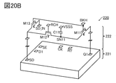
- FIG. 19 is a diagram illustrating a configuration example of a CPU.
- 20A and 20B are diagrams illustrating a configuration example of a CPU.
- FIG. 21 is a schematic cross-sectional view showing a configuration example of a semiconductor device.
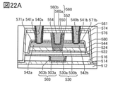
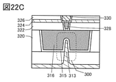
- 22A to 22C are schematic cross-sectional views showing a configuration example of a transistor.
- FIG. 23 is a schematic cross-sectional view showing a configuration example of the semiconductor device.
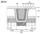
- 24A and 24B are schematic cross-sectional views showing a configuration example of a transistor.
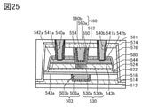
- FIG. 25 is a schematic cross-sectional view showing a configuration example of the transistor.
- FIG. 26A is a diagram for explaining the classification of the crystal structure of IGZO, FIG.
- FIG. 26B is a diagram for explaining the XRD spectrum of crystalline IGZO
- FIG. 26C is a diagram for explaining the microelectron diffraction pattern of crystalline IGZO.
- .. 27A is a perspective view showing an example of a semiconductor wafer
- FIG. 27B is a perspective view showing an example of a chip
- FIGS. 27C and 27D are perspective views showing an example of an electronic component.
- FIG. 28 is a perspective view showing an example of an electronic device.
- 29A to 29C are perspective views showing an example of an electronic device.
- the ordinal numbers "1st”, “2nd”, and “3rd” are added to avoid confusion of the components. Therefore, the number of components is not limited. Moreover, the order of the components is not limited. Further, for example, the component referred to in “first” in one of the embodiments of the present specification and the like is regarded as another embodiment or the component referred to in “second” in the scope of claims. It is possible. Further, for example, the component referred to in “first” in one of the embodiments of the present specification and the like may be omitted in another embodiment or in the scope of claims.
- the power supply potential VDD may be abbreviated as potential VDD, VDD, etc. This also applies to other components (eg, signals, voltages, circuits, elements, electrodes, wiring, etc.).
- the code is used for identification such as "_1”, “_2”, “[n]", “[m, n]”. May be added and described.
- the second wiring GL is described as wiring GL [2].
- the semiconductor device refers to all devices that can function by utilizing the semiconductor characteristics.
- a semiconductor circuit, an arithmetic unit, and a storage device, including a semiconductor element such as a transistor, are one aspect of a semiconductor device. It may be said that a display device (liquid crystal display device, light emission display device, etc.), projection device, lighting device, electro-optical device, power storage device, storage device, semiconductor circuit, image pickup device, electronic device, and the like have a semiconductor device.
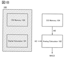
- FIG. 1A and 1B are diagrams for explaining the semiconductor device 100, which is one aspect of the present invention.
- the semiconductor device 100 includes a digital calculator 101, an analog semiconductor 102, an oxide semiconductor memory (OS Memory: Oxide Semiconductor Memory) 103, and an oxide semiconductor memory (OS Memory) 104. , Have.
- the digital arithmetic unit 101 preferably has a transistor (Si transistor) having silicon in the channel forming region.
- the analog arithmetic unit 102 preferably has a transistor (OS transistor) having an oxide semiconductor in the channel forming region.
- the oxide semiconductor memory 103 and the oxide semiconductor memory 104 have an OS transistor.
- the semiconductor device 100 functions as an accelerator capable of processing the product-sum calculation, and the digital arithmetic unit 101 and the analog arithmetic unit 102 can be used properly according to the type of calculation.
- FIG. 1A shows a state in which the digital arithmetic unit 101 is operated
- FIG. 1B shows a state in which the analog arithmetic unit 102 is operated.
- the analog calculator 102 is in a non-operating state while the digital calculator 101 is in operation.
- the digital arithmetic unit 101 is in a non-operating state while the analog arithmetic unit 102 is in operation.
- the digital calculator 101 performs a product-sum calculation using the weight data W1 input from the oxide semiconductor memory 103 and the input data A1, and outputs the result as output data MAC1. ..
- the weight data W1 output by the oxide semiconductor memory 103 is output as digital data.
- the OS transistor provided in the oxide semiconductor memory 103 has an extremely small leakage current, that is, a current flowing between the source and the drain in the off state.
- the oxide semiconductor memory 103 can be used as a non-volatile memory by holding a charge corresponding to the data in the memory circuit using the characteristic that the leakage current is extremely small.
- the oxide semiconductor memory 103 with a memory circuit capable of reading the held data without destroying it (non-destructive reading). As a result, processing using the same weight data can be repeated at a high arithmetic processing speed. Therefore, it is possible to speed up the parallel processing of the product-sum operation of the neural network by repeating the data reading operation many times.
- the digital arithmetic unit 101 it is preferable that the input data A1 and the weight data W1 are digital data resistant to noise. As a result, the digital arithmetic unit 101 can perform arithmetic processing with high accuracy.
- the semiconductor device 100 can perform high-precision and high-performance arithmetic processing. Therefore, the semiconductor device 100 can efficiently perform processing using the same weight data as in the case of a convolutional neural network.
- the detailed configurations and specific examples of the oxide semiconductor memory 103 and the digital arithmetic unit 101 will be described in the embodiments described later.
- the analog calculator 102 performs a product-sum calculation using the weight data W2 input from the oxide semiconductor memory 104 and the input data A2, and outputs the result as output data MAC2. .
- the weight data W2 output by the oxide semiconductor memory 104 is output as analog data.
- the OS transistor used in the analog arithmetic unit 102 and the oxide semiconductor memory 104 has a lower off current than the Si transistor, and can take a large range of the gate voltage operating in the subthreshold region. Therefore, in the analog arithmetic unit 102 and the oxide semiconductor memory 104, the OS transistor can be driven relatively easily in the subthreshold region where the current value is small.
- the semiconductor device 100 can perform arithmetic processing with low power consumption. Therefore, it is possible to efficiently perform an operation process of frequently rewriting the weight data, such as a fully coupled operation, in the semiconductor device 100.
- the detailed configurations and specific examples of the oxide semiconductor memory 104 and the analog arithmetic unit 102 will be described in the embodiments described later.
- the semiconductor device 100 shown in the present embodiment operates the digital arithmetic unit 101 when repeatedly performing arithmetic processing using the same weight data, and is analog when the weight data is frequently rewritten.
- the arithmetic unit 102 can be operated. In this way, by properly using the digital arithmetic unit 101 and the analog arithmetic unit 102, it is possible to perform arithmetic processing with high accuracy, high performance, and low power consumption as a whole.
- the semiconductor device 100 shown in the present embodiment can also process a plurality of operations in parallel.
- the plurality of operations include a repetitive operation using the same weight data and an operation in which the weight data is frequently rewritten
- the digital arithmetic unit 101 and the analog arithmetic unit 102 may be operated in parallel. .. That is, while the digital arithmetic unit 101 processes the repetitive operation using the same weight data, the analog arithmetic unit 102 can process the operation of frequently rewriting the weight data in parallel.
- the digital arithmetic unit 101 can perform the next convolutional operation in parallel while the analog arithmetic unit 102 processes the full-coupling operation.
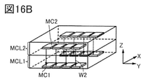
- FIG. 2A shows an example in which a digital arithmetic unit 101 is formed on a silicon substrate, and an analog arithmetic unit 102, an oxide semiconductor memory 103, and an oxide semiconductor memory 104 are arranged on the digital arithmetic unit 101.
- an xy plane is set substantially parallel to the upper surface of the silicon substrate, and an element layer forming the analog arithmetic unit 102, the oxide semiconductor memory 103, and the oxide semiconductor memory 104 is provided above the z-axis direction.
- the semiconductor device 100 that functions as an accelerator can be highly integrated, and the arithmetic processing speed per unit area can be improved. This makes it possible to reduce the size of the semiconductor device 100.
- the oxide semiconductor memory 103 it is preferable to superimpose the oxide semiconductor memory 103 on the digital arithmetic unit 101.
- the distance of the wiring for electrically connecting the oxide semiconductor memory 103 and the digital arithmetic unit 101 can be shortened. Therefore, it is possible to improve the processing speed when rewriting the weight data of the digital arithmetic unit 101 and reduce the power consumption in the processing.
- each part of the semiconductor device 100 shown in the present embodiment is not limited to the arrangement shown in FIG. 2A.
- the element layer forming the oxide semiconductor memory 103 may be laminated with the analog arithmetic unit 102 and the element layer forming the oxide semiconductor memory 104. With such a configuration, the semiconductor device 100 can be further miniaturized.
- the Si transistor is used for the digital arithmetic unit 101
- the present embodiment is not limited to this, and the configuration in which the Si transistor is used for the analog arithmetic unit 102 is also possible.
- the configuration in which the Si transistor is used for the digital arithmetic unit 101 and the OS transistor is used for the analog arithmetic unit 102 is shown, but the present embodiment is not limited to this.
- both the digital arithmetic unit 101 and the analog arithmetic unit 102 may be configured to use an OS transistor.
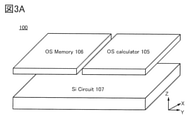
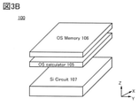
- the oxide semiconductor arithmetic unit (OS Calculator) 105 and the oxide semiconductor memory (OS Memory) 106 can be arranged on the silicon circuit (Si Silicon) 107.
- the oxide semiconductor arithmetic unit 105 is an arithmetic unit formed of an OS transistor, and a digital arithmetic unit and an analog arithmetic unit are mounted together.
- the oxide semiconductor memory 106 has a function of supplying weight data to the oxide semiconductor arithmetic unit 105.
- the silicon circuit 107 may have any function, and may function as, for example, a drive circuit, a read circuit, a storage circuit, an arithmetic circuit, or the like.
- the element layer forming the oxide semiconductor arithmetic unit 105 and the oxide semiconductor memory 106 is provided on the silicon substrate.
- each part of the semiconductor device 100 shown in the present embodiment is not limited to the arrangement shown in FIG. 3A.
- the element layer forming the oxide semiconductor memory 106 may be laminated on the element layer forming the oxide semiconductor arithmetic unit 105.
- the semiconductor device 100 that functions as an accelerator can be highly integrated, and the arithmetic processing speed per unit area can be improved. This makes it possible to reduce the size of the semiconductor device 100.
- the above-mentioned semiconductor device 100 can constitute a semiconductor device having a CPU 110 and a bus 120. With such a configuration, a part of the operation of the program executed by the CPU 110 can be executed by the semiconductor device 100 functioning as an accelerator.
- the CPU 110 has a function of performing general-purpose processing such as execution of an operating system, control of data, various operations, or execution of a program.
- the CPU 110 has a CPU core 200 and a backup circuit 222.
- the CPU core 200 corresponds to one or more CPU cores.
- the CPU 110 can hold the data in the CPU core 200 even if the supply of the power supply voltage is stopped by the backup circuit 222.
- the supply of the power supply voltage can be controlled by electrical disconnection from the power supply domain (power domain) by a power switch or the like.
- the backup circuit 222 for example, an OS memory having an OS transistor is suitable.
- bus 120 electrically connects the CPU 110 and the semiconductor device 100 that functions as an accelerator. That is, the CPU 110 and the semiconductor device 100 functioning as an accelerator can transmit data via the bus 120.
- one aspect of the present invention can provide a semiconductor device with low power consumption.
- one aspect of the present invention can provide a semiconductor device with improved arithmetic processing speed.
- one aspect of the present invention can provide a semiconductor device with improved calculation accuracy.
- one aspect of the present invention can provide a miniaturized semiconductor device.
- FIG. 5A is a diagram for explaining the semiconductor device 10 which is one aspect of the present invention.
- the semiconductor device 10 is a part of the semiconductor device 100, and has the digital arithmetic unit 101 and the oxide semiconductor memory 103 shown in the above embodiment.
- the semiconductor device 10 has a function as an accelerator that executes a program (also called a kernel or a kernel program) called from a host program.
- the semiconductor device 10 can perform, for example, parallel processing of matrix operations in graphic processing, parallel processing of product-sum operations in a neural network, parallel processing of floating-point operations in science and technology calculations, and the like.
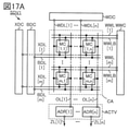
- the semiconductor device 10 has a memory circuit unit 20 (also referred to as a memory cell array), an arithmetic circuit 30, and a switching circuit 40.
- the arithmetic circuit 30 corresponds to the digital arithmetic unit 101 shown in the previous embodiment
- the memory circuit unit 20 corresponds to the oxide semiconductor memory 103 shown in the previous embodiment.
- the arithmetic circuit 30 and the switching circuit 40 are provided on the layer 11 having a transistor in the xy plane in the figure.
- the memory circuit unit 20 is provided on the layer 12 having a transistor on the xy plane in the figure.
- the layer 11 has a transistor (Si transistor) having silicon in the channel forming region.
- the layer 12 has a transistor (OS transistor) having an oxide semiconductor in the channel forming region.
- the layer 11 and the layer 12 are provided in different layers in a direction substantially perpendicular to the xy plane (in the z direction in FIG. 5A). Therefore, the semiconductor device 10 shown in FIG. 5B has a laminated structure similar to that of the digital arithmetic unit 101 and the oxide semiconductor memory 103 shown in FIG. 2A or FIG. 2B.
- the memory circuit unit 20 composed of the OS transistor can be provided so as to be stacked with the arithmetic circuit 30 and the switching circuit 40 which can be configured by the Si transistor. That is, the memory circuit unit 20 is provided on the substrate on which the arithmetic circuit 30 and the switching circuit 40 are provided. Therefore, the memory circuit unit 20 can be arranged without increasing the circuit area. By setting the area where the memory circuit unit 20 is provided on the substrate on which the arithmetic circuit 30 and the switching circuit 40 are provided, the memory circuit unit 20 and the arithmetic circuit 30 and the switching circuit 40 may be arranged on the same layer. In comparison, the storage capacity required for arithmetic processing in the semiconductor device 10 that functions as an accelerator can be increased. By increasing the storage capacity, it is possible to reduce the number of times of data transfer required for arithmetic processing from the external storage device to the semiconductor device, so that power consumption can be reduced.
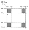
- the memory circuit unit 20 shows a plurality of memory circuit units 20_1 to 20_1 as an example. Each memory circuit unit has a plurality of memory circuits 21. The plurality of memory circuits 21 are connected to the switching circuit 40 via wirings LBL_1 to LBL_1 (also referred to as local bit lines and read bit lines) in each of the memory circuit units 20_1 to 20_1 as shown in FIG. 5A.
- LBL_1 to LBL_1 also referred to as local bit lines and read bit lines
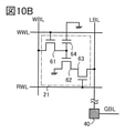
- the memory circuit 21 can have a NOSRAM circuit configuration.
- NOSRAM registered trademark
- NOSRAM refers to a memory in which the memory cell is a 2-transistor type (2T) or 3-transistor type (3T) gain cell and the access transistor is an OS transistor.
- the memory circuit 21 is a memory composed of OS transistors.
- the layer 12 having the memory circuit 21 can be laminated on the layer 11 having the arithmetic circuit 30 and the switching circuit 40. Since the memory circuit unit 20 having the memory circuit 21 is provided on the layer 11 having the arithmetic circuit 30 and the switching circuit 40, it is possible to reduce the area overhead due to having the memory circuit unit 20.
- the OS transistor has an extremely small leakage current, that is, the current that flows between the source and drain in the off state.
- the NOSRAM can be used as a non-volatile memory by holding a charge corresponding to the data in the memory circuit using the characteristic that the leakage current is extremely small.
- NOSRAM can read the held data without destroying it (non-destructive reading), it is suitable for parallel processing of the product-sum operation of the neural network in which the data reading operation is repeated many times.
- a memory having an OS transistor such as NOSRAM or DOSRAM (hereinafter, also referred to as OS memory) is suitable. Since the bandgap of the metal oxide that functions as an oxide semiconductor is 2.5 eV or more, the OS transistor has a minimum off current. As an example, when the voltage between the source and drain is 3.5 V and the room temperature (25 ° C) is normal, the off current per 1 ⁇ m of channel width is less than 1 ⁇ 10-20 A, less than 1 ⁇ 10-22 A , or 1 ⁇ 10. It can be less than -24A . Therefore, the OS memory has an extremely small amount of charge leaked from the holding node via the OS transistor. Therefore, since the OS memory can function as a non-volatile memory circuit, power gating of the semiconductor device 10 becomes possible.
- OS memory such as NOSRAM or DOSRAM
- Semiconductor devices with high density and integrated transistors may generate heat due to the drive of the circuit. Due to this heat generation, the temperature of the transistor rises, which may change the characteristics of the transistor, resulting in a change in field effect mobility or a decrease in operating frequency. Since the OS transistor has higher thermal resistance than the Si transistor, the field effect mobility does not easily change due to the temperature change, and the operating frequency does not easily decrease. Further, the OS transistor tends to maintain the characteristic that the drain current increases exponentially with respect to the gate-source voltage even when the temperature rises. Therefore, by using the OS transistor, stable operation can be performed in a high temperature environment.
- the metal oxides applied to the OS transistor are Zn oxide, Zn-Sn oxide, Ga-Sn oxide, In-Ga oxide, In-Zn oxide, and In-M-Zn oxide (M is: Ti, Ga, Y, Zr, La, Ce, Nd, Sn or Hf) and the like.
- M is: Ti, Ga, Y, Zr, La, Ce, Nd, Sn or Hf
- oxides containing indium and zinc include aluminum, gallium, ittrium, copper, vanadium, beryllium, boron, silicon, titanium, iron, nickel, germanium, zirconium, molybdenum, lanthanum, cerium, neodymium, hafnium, tantalum, and tungsten. , Magnesium, etc. may be included, or a plurality of species may be contained.
- the metal oxide applied to the semiconductor layer is preferably a metal oxide having a crystal portion such as CAAC-OS, CAC-OS, and nc-OS.
- CAAC-OS is an abbreviation for c-axis-aligned crystalline oxide semiconductor ductor.
- CAC-OS is an abbreviation for Cloud-Aligned Complex oxide semiconductor semiconductor.
- nc-OS is an abbreviation for nanocrystalline oxide semiconductor ductor.
- CAAC-OS has a c-axis orientation and has a crystal structure in which a plurality of nanocrystals are connected in the ab plane direction and have strain.
- the strain refers to a region where the orientation of the lattice arrangement changes between a region in which the lattice arrangement is aligned and a region in which another lattice arrangement is aligned in the region where a plurality of nanocrystals are connected.
- the CAC-OS has a function of flowing electrons (or holes) as carriers and a function of not flowing electrons as carriers. By separating the function of flowing electrons and the function of not flowing electrons, both functions can be maximized. That is, by using CAC-OS in the channel formation region of the OS transistor, both a high on current and an extremely low off current can be realized.
- OS transistors Since metal oxides have a large bandgap, electrons are not easily excited, and the effective mass of holes is large, OS transistors may be less prone to avalanche collapse than general Si transistors. .. Therefore, for example, deterioration of hot carriers due to avalanche breakdown can be suppressed. By suppressing hot carrier deterioration, it is possible to drive an OS transistor with a high drain voltage.
- the OS transistor is a storage type transistor that has a large number of electrons as carriers. Therefore, the influence of DIBL (Drain-Induced Barrier Lowering), which is one of the short-channel effects, is smaller than that of an inverting transistor (typically, a Si transistor) having a pn junction. That is, the OS transistor has a higher resistance to the short channel effect than the Si transistor.
- DIBL Drain-Induced Barrier Lowering
- the OS transistor Since the OS transistor has high resistance to the short channel effect, the channel length can be reduced without deteriorating the reliability of the OS transistor, so that the degree of circuit integration can be increased by using the OS transistor. As the channel length becomes finer, the drain electric field becomes stronger, but as mentioned above, the OS transistor is less likely to undergo avalanche breakdown than the Si transistor.
- the OS transistor has high resistance to the short channel effect, it is possible to make the gate insulating film thicker than the Si transistor. For example, even in a fine transistor having a channel length and a channel width of 50 nm or less, it may be possible to provide a thick gate insulating film of about 10 nm. By thickening the gate insulating film, the parasitic capacitance can be reduced, so that the operating speed of the circuit can be improved. Further, by making the gate insulating film thicker, the leakage current through the gate insulating film is reduced, which leads to a reduction in static current consumption.
- the semiconductor device 10 has the memory circuit 21 which is the OS memory, so that the data can be held even if the supply of the power supply voltage is stopped. Therefore, power gating of the semiconductor device 10 becomes possible, and power consumption can be significantly reduced.
- the data stored in the memory circuit 21 is data (weight data) corresponding to the weight parameter used in the product-sum operation of the neural network.
- weight data may be analog data. Since the NOSRAM can hold the potential of the analog value, the data can be appropriately converted into the digital data and used.
- the memory circuit 21 capable of holding analog data represents weight data having a high number of bits, it can hold the memory circuit without increasing the number of memory circuits.
- the switching circuits 40_1 to 40_4 shown as an example of the switching circuit 40 have a function of selecting the potentials of the wirings LBL_1 to LBL_1 extending from each of the plurality of memory circuit units 20_1 to 20_1 and transmitting them to the wiring GBL (also referred to as a global bit line). Has.
- the output terminals of the switching circuits 40_1 to 40_1 are connected to the wiring GBL.
- the switching circuit 40 needs to prevent the output potentials of the selected switching circuit 40 and the non-selected switching circuit 40 from being supplied at the same time to generate a through current.
- a three-state buffer in which the state of the output potential is controlled by a control signal can be used as the switching circuit 40.
- the selected switching circuit outputs the input potential as a buffer, and the output of the non-selected switching circuit has high impedance, so that it is possible to avoid supplying the output potentials at the same time.
- the switching circuit 40 is preferably composed of a Si transistor. With this configuration, it is possible to switch the connection state at high speed.
- the arithmetic circuits 30_1 to 30_4 shown as an example of the arithmetic circuit 30 have a function of repeatedly executing the same processing such as a product-sum operation.
- Digital data is preferable as the input data and weight data input for the product-sum calculation in the calculation circuit 30.
- Digital data is less susceptible to noise. Therefore, the arithmetic circuit 30 is suitable for performing arithmetic processing that requires highly accurate arithmetic results.
- the arithmetic circuit 30 is preferably composed of a Si transistor. With this configuration, it can be provided by stacking with an OS transistor.
- the arithmetic circuits 30_1 to 30_1 are given weight data held in the memory circuit 21 via the wirings LBL_1 to LBL_1 and the wiring GBL. Further, the arithmetic circuits 30_1 to 30_1 are given input data (A 1 , A 2 , A 3 , A 4 ) input from the outside. The arithmetic circuits 30_1 to 30_1 perform arithmetic processing of the product-sum operation using the weight data held in the memory circuit 21 and the input data input from the outside.
- the weight data given to the arithmetic circuits 30_1 to 30_1 is weight data in which the weight data selected by the plurality of memory circuit units 20_1 to 20_1 is switched by the switching circuits 40_1 to 40_1 and given via the wiring GBP. That is, in the arithmetic circuits 30_1 to 30_1, arithmetic processing using the same weight data, for example, a product-sum operation can be performed. Therefore, the semiconductor device 10 in one aspect of the present invention can efficiently perform processing using the same weight data as in the convolutional neural network.
- the weight data given to the arithmetic circuits 30_1 to 30_1 can be given to the wiring GBL by switching the data previously given to the wiring LBL_1 to LBL_1 by the switching circuits 40_1 to 40_1, so that the weight data given to the wiring GBL is , It can be switched at a speed according to the electrical characteristics of the Si transistor. Therefore, even if the period for reading the weight data from the memory circuit units 20_1 to 20_1 to the wirings LBL_1 to LBL_1 is long, the weight data can be read out to the wirings LBL_1 to LBL_1 in advance at high speed. It can be switched and processed.
- the wiring LBL extending from the memory circuit unit 20 toward the switching circuit 40 is wiring for transmitting the weight data W data from the layer 12 to the layer 11 as shown in FIG. 5B.
- the wiring LBL is preferably shortened in order to reduce the energy consumption associated with charging and discharging. That is, it is preferable that the switching circuit 40 is arranged so as to be dispersed in the xy plane of the layer 11 so as to be close to the wiring LBL (arrow extending in the z direction in the drawing) provided extending in the z direction.
- the arithmetic circuits 30_1 to 30_1 are configured to provide arithmetic circuits 30_1 to 30_1 for each wiring LBL_1 to LBL_1, that is, for each row (Column), which is a bit line for reading the memory circuit 21 (Column-Parallel Calibration).
- LBL_1 to LBL_1 that is, for each row (Column), which is a bit line for reading the memory circuit 21 (Column-Parallel Calibration).
- the data bus size 32 bits, etc.
- the power generated by the memory access can be reduced, and the heat generation and power consumption can be reduced.
- the increase can be suppressed.
- the wiring distance can be shortened by stacking, the parasitic capacitance generated in the signal line can be reduced, so that the power consumption can be reduced.
- FIG. 6A a block diagram including a semiconductor device 10, a CPU 110, and a bus 120 that function as AI accelerators will be described.
- the CPU 110 and the bus 120 correspond to those shown in the previous embodiment.
- FIG. 6A illustrates the CPU 110 and the bus 120 in addition to the semiconductor device 10 described with reference to FIGS. 5A and 5B.
- the CPU 110 has a CPU core 200 and a backup circuit 222.
- the semiconductor device 10 that functions as an accelerator illustrates a drive circuit 50, memory circuit units 20_1 to 20_N (N is a natural number of 2 or more), a memory circuit 21, a switching circuit 40, and arithmetic circuits 30_1 to 30_N.
- the CPU 110 has a function of performing general-purpose processing such as execution of an operating system, control of data, various operations, and execution of a program.
- the CPU 110 has a CPU core 200.
- the CPU core 200 corresponds to one or more CPU cores.
- the CPU 110 has a backup circuit 222 that can hold the data in the CPU core 200 even if the supply of the power supply voltage is stopped.
- the supply of the power supply voltage can be controlled by electrical disconnection from the power supply domain (power domain) by a power switch or the like.
- the power supply voltage may be referred to as a drive voltage.
- As the backup circuit 222 for example, an OS memory having an OS transistor is suitable.
- the backup circuit 222 composed of the OS transistor can be provided so as to be laminated with the CPU core 200 that can be configured with the Si transistor. Since the area of the backup circuit 222 is smaller than the area of the CPU core 200, the backup circuit 222 can be arranged on the CPU core 200 without increasing the circuit area.
- the backup circuit 222 has a function of holding the register data of the CPU core 200.
- the backup circuit 222 is also referred to as a data holding circuit. The details of the configuration of the CPU core 200 including the backup circuit 222 including the OS transistor will be described in the fifth embodiment.
- the memory circuit units 20_1 to 20_N output the weight data W1 to WN held in the memory circuit 21 to the switching circuit 40 via the wiring LBL (not shown), respectively.
- the switching circuit 40 outputs the selected weight data to each arithmetic circuit 30_1 to 30_N as weight data WSEL via the wiring GBL (not shown).
- the drive circuit 50 outputs the input data A1 to AN to the arithmetic circuits 30_1 to 30_N via the input data line.
- the drive circuit 50 has a function of outputting a signal for controlling the writing and reading of weight data in the memory circuit units 20_1 to 20_N. Further, the drive circuit 50 holds a circuit for giving input data to the arithmetic circuits 30_1 to 30_N to execute the product-sum operation of the neural network, and the output data obtained by the product-sum operation of the neural network. Has a function.
- the bus 120 electrically connects the CPU 110 and the semiconductor device 10. That is, the CPU 110 and the semiconductor device 10 can transmit data via the bus 120.
- FIG. 6B is a diagram for explaining the positional relationship of each configuration when N is 6 in the semiconductor device 10 shown in FIG. 6A.
- the memory circuit units 20_1 to 20_1 composed of OS transistors and the arithmetic circuits 30_1 to 30_6 extend in a direction substantially perpendicular to the surface of the substrate on which the drive circuit 50, the switching circuit 40, and the arithmetic circuits 30_1 to 30_1 are provided. It is electrically connected via the wirings LBL_1 to LBL_1 provided therein.
- approximately vertical means a state in which the particles are arranged at an angle of 85 degrees or more and 95 degrees or less.
- the X direction, the Y direction, and the Z direction shown in FIG. 6B and the like are directions orthogonal to or intersecting each other. Further, the X direction and the Y direction are parallel or substantially parallel to the substrate surface, and the Z direction is perpendicular or substantially perpendicular to the substrate surface.
- the memory circuit units 20_1 to 20_1 each have a memory circuit 21.
- the memory circuit units 20_1 to 20_1 may be referred to as a device memory or a shared memory.
- the memory circuit 21 has a transistor 22.
- oxide semiconductor metal oxide
- the memory circuit 21 composed of the OS transistor described above can be used.
- the plurality of memory circuits 21 included in the memory circuit units 20_1 to 20_1 are connected to the wirings LBL_1 to LBL_1, respectively.
- the wirings LBL_1 to LBL_6 are connected to the switching circuit 40 via the wiring extending in the z direction.
- the switching circuit 40 is configured to amplify the potential of any one of the wirings LBL_1 to LBL_6 and transmit it to the wiring GBL. With this configuration, the weight data given to the wiring GBL can be switched at high speed by controlling the switching circuit 40.
- the calculation circuits 30_1 to 30_1 perform a calculation based on the weight data input via the wiring GBL and the input data A IN given from the drive circuit 50 via the input data line. Since the memory circuit units 20_1 to 20_1 for holding the weight data can be arranged in the upper layer, the arithmetic circuits 30_1 to 30_1 can be efficiently arranged. Therefore, the input data line extending from the drive circuit 50 can be shortened, and the power consumption and speed of the semiconductor device 10 can be reduced.
- each configuration of FIG. 6B is shown as a block diagram. It will be described that the weight data W1 to W6 are read out from the memory circuits 21 in the six memory circuit units 20_1 to 20_1 to the wirings LBL_1 to LBL_1. Further, the switching circuit 40 will be described as switching circuits 40_1 to 40_1 connected to the wirings LBL_1 to LBL_1. Further, the weight data selected from the weight data W1 to W6 in the switching circuit 40 and given to the wiring GBL will be described as the weight data W SEL . Input data A 1 to A 6 are given to the arithmetic circuits 30_1 to 30_1, respectively, and the output data MAC 1 to MAC 6 will be obtained.
- the wiring LBL P extending in the vertical direction connecting the upper layer and the lower layer in the wirings LBL_1 to LBL_1 is shorter than the wiring extending in the horizontal direction. Therefore, the parasitic capacitance of the wirings LBL_1 to LBL_1 can be reduced, the charge required for charging and discharging the wiring can be reduced, the power consumption can be reduced, and the calculation efficiency can be improved. Further, reading from the memory circuit 21 to the wirings LBL_1 to LBL_1 can be performed at high speed.
- the arithmetic circuits 30_1 to 30_1 can perform arithmetic processing using the same weight data via the wiring GBL. This configuration is suitable for arithmetic processing of a convolutional neural network that performs arithmetic processing using the same weight data.
- FIG. 7B is an example of a circuit configuration applicable to the switching circuit 40 illustrated in FIG. 7A.
- the three-state buffer illustrated in FIG. 7B has a function of amplifying and transmitting the potential of the wiring LBL to the wiring GBL in response to the control signal EN.
- the switching circuit 40 can be regarded as a multiplexer. It has a function to select one from a plurality of input signals.
- FIG. 8 shows a timing chart for explaining the operation of the configuration described with reference to FIG. 7A.
- the semiconductor device 10 performs arithmetic processing according to the toggle operation of the clock signal CLK (for example, times T1 to T7). By increasing the frequency of the clock signal CLK, it is possible to speed up the arithmetic processing.
- the weight data selected from the wiring LBL to the wiring GBL in the switching circuit 40 is read in advance to the wiring LBL_1 to LBL_1, so that the wiring GBL data giving the weight data can be obtained. You can switch at high speed.
- the weight data W1 may be read into the wiring LBL_1 at the time T1
- the switching circuit 40 may be switched at the time T6, and the weight data W1 may be output from the wiring LBL_1 to the wiring GBL.
- the weight data is switched according to the clock signal CLK by reading the weight data to the wiring LBL and selecting the weight data in the wiring GBL by different times. Can be configured to perform.
- FIG. 9A shows a specific configuration example of the arithmetic circuit.
- FIG. 9A illustrates a configuration example of a calculation circuit 30 capable of performing a product-sum calculation of input data of 8-bit weight data.
- the multiplication circuit 24, the addition circuit 25, and the register 26 are illustrated.
- the 16-bit data multiplied by the multiplication circuit 24 is input to the addition circuit 25.
- the output of the addition circuit 25 is held in the register 26, and the product-sum operation is performed by adding the data to be multiplied by the multiplication circuit 24 and the addition circuit 25.
- the register is controlled by the clock signal CLK and the reset signal reset_B. Note that " ⁇ " in "17 + ⁇ " in the figure indicates a carry generated by adding multiplication data. With this configuration, it is possible to obtain an output data MAC corresponding to the product-sum operation of the weight data W SEL and the input data A IN .
- FIG. 9A the configuration is described as performing arithmetic processing using 8-bit data, but one aspect of the present invention can also be applied to a configuration using 1-bit data.
- the configuration is illustrated in FIG. 9B in the same manner as in FIG. 9A.
- arithmetic processing may be performed according to the number of bits.
- FIG. 10A is a diagram illustrating an example of a circuit configuration applicable to the memory circuit unit 20 included in the semiconductor device 10 of the present invention.
- writing word lines WWL_1 to WWL_M are arranged side by side in the matrix direction of M rows and N columns (M and N are natural numbers of 2 or more).
- WBL_N and wiring LBL_1 to LBL_N are illustrated.
- the memory circuit 21 connected to each word line and bit line is illustrated.
- FIG. 10B is a diagram illustrating a circuit configuration example applicable to the memory circuit 21.
- the memory circuit 21 includes a transistor 61, a transistor 62, a transistor 63, and a capacitive element 64 (also referred to as a capacitor).
- One of the source and drain of the transistor 61 is connected to the writing bit line WBL.
- the gate of the transistor 61 is connected to the writing word line WWL.
- the other of the source or drain of the transistor 61 is connected to one electrode of the capacitive element 64 and the gate of the transistor 62.
- One of the source or drain of the transistor 62 and the other electrode of the capacitive element 64 are connected to a wire that provides a fixed potential, eg, a ground potential.
- the other of the source or drain of the transistor 62 is connected to one of the source or drain of the transistor 63.
- the gate of the transistor 63 is connected to the read word line RWL.
- the other of the source or drain of the transistor 63 is connected to the wiring LBL.
- the wiring LBL is connected to the wiring GBL via the switching circuit 40. As described above, the wiring LBL is connected to the switching circuit 40 via wiring provided so as to extend in a direction substantially perpendicular to the surface of the substrate on which the arithmetic circuit 30 is provided.
- the circuit configuration of the memory circuit 21 shown in FIG. 10B corresponds to the NOSRAM of the 3-transistor type (3T) gain cell.
- the transistor 61 to the transistor 63 are OS transistors.
- the OS transistor has an extremely small leakage current, that is, a current flowing between the source and the drain in the off state.
- the NOSRAM can be used as a non-volatile memory by holding a charge corresponding to the data in the memory circuit using the characteristic that the leakage current is extremely small.
- the circuit configuration applicable to the memory circuit 21 of FIG. 10A is not limited to the 3T type NOSRAM of FIG. 10B.
- it may be a circuit corresponding to the DOSRAM shown in FIG. 11A.
- FIG. 11A illustrates a memory circuit 21A having a transistor 61A and a capacitive element 64A.
- the transistor 61A is an OS transistor.
- the memory circuit 21A illustrates an example of being connected to a bit line BL, a word line WL, and a back gate line BGL.
- the circuit configuration applicable to the memory circuit 21 of FIG. 10A may be a circuit corresponding to the 2T type NOSRAM shown in FIG. 11B.
- FIG. 11B illustrates a memory circuit 21B having a transistor 61B, a transistor 62B, and a capacitive element 64B.
- the transistor 61B and the transistor 62B are OS transistors.
- the transistor 61B and the transistor 62B may be an OS transistor in which a semiconductor layer is arranged in different layers, or an OS transistor in which a semiconductor layer is arranged in the same layer.
- the memory circuit 21B illustrates an example of being connected to a write bit line WBL, a read bit line RBL, a write word line WWL, a read word line RWL, a source line SL, and a backgate line BGL.
- the circuit configuration applicable to the memory circuit 21 of FIG. 10A may be a circuit in which the 3T type NOSRAM shown in FIG. 11C is combined.
- FIG. 11C illustrates a memory circuit 21C having a memory circuit 21_P capable of holding data having different logics and a memory circuit 21_N.
- FIG. 11C illustrates a memory circuit 21_P having a transistor 61_P, a transistor 62_P, a transistor 63_P and a capacitive element 64_P, and a memory circuit 21_N having a transistor 61_N, a transistor 62_N, a transistor 63_N and a capacitive element 64_N.
- Each transistor included in the memory circuit 21_P and the memory circuit 21_N is an OS transistor.
- Each transistor included in the memory circuit 21_P and the memory circuit 21_N may be an OS transistor in which a semiconductor layer is arranged in different layers, or an OS transistor in which a semiconductor layer is arranged in the same layer.
- the memory circuit 21C shows an example of being connected to a writing bit line WBL_P, a wiring LBL_P, a writing bit line WBL_N, a wiring LBL_N, a writing word line WWL, and a reading word line RWL.
- the memory circuit 21C holds data having different logics, reads data having different logics to the wiring LBL_P and the wiring LBL_N, and can output the data to the wiring GBL_P and the wiring GBL_N via the switching circuit 40 in the same manner as in FIG. ..
- an exclusive OR circuit may be provided so that the data corresponding to the multiplication of the data held in the memory circuit 21_P and the memory circuit 21_N is output to the wiring LBL.
- XOR circuit exclusive OR circuit
- FIG. 12 illustrates the flow of arithmetic processing of a convolutional neural network.
- FIG. 12 illustrates an input layer 90A, an intermediate layer 90B (also referred to as a hidden layer), and an output layer 90C.
- the input layer 90A illustrates an input data input process 91 (shown as Input in the figure).
- convolution calculation processes 92, 93, 95 shown as Conv. In the figure
- a plurality of pooling calculation processes 94, 96 shown as Pool. In the figure
- the fully combined operation process 97 (shown as Full in the figure) is illustrated.
- the flow of arithmetic processing in the input layer 90A, the intermediate layer 90B, and the output layer 90C is an example, and in the actual arithmetic processing of the convolutional neural network, other arithmetic processing such as softmax arithmetic may be performed.
- the convolutional operation processes 92, 93, and 95 are performed a plurality of times.
- the operation process using the same weight data is performed. Therefore, by applying the configuration of one aspect of the present embodiment in which the arithmetic processing using the same weight data is performed, it is possible to achieve both the operating speed and the low power consumption.
- the fully coupled arithmetic processing 97 is calculated by using the analog arithmetic unit 102 and the oxide semiconductor memory 104. Since the analog arithmetic unit 102 and the oxide semiconductor memory 104 can be driven in the sub-threshold region, low power consumption can be achieved.
- FIG. 13 shows a detailed block diagram of the semiconductor device 10.
- FIG. 13 in addition to the configurations corresponding to the memory circuit unit 20, the memory circuit 21, the arithmetic circuit 30, the switching circuit 40, the layer 11, and the layer 12, which are described in FIGS. 5A and 5B, and FIGS.
- the configuration example of the drive circuit 50 shown in 6A and 6B is illustrated.
- the controller 71, the row decoder 72, the word line driver 73, the column decoder 74, the write driver 75, the precharge circuit 76, and the input / output buffer 81 are configured to correspond to the drive circuit 50 described with reference to FIGS. 6A and 6B. And the arithmetic control circuit 82 is illustrated.
- FIG. 14A is a diagram in which a block that controls the memory circuit unit 20 is extracted for each configuration shown in FIG. 14A, the controller 71, the row decoder 72, the word line driver 73, the column decoder 74, the write driver 75, and the precharge circuit 76 are extracted and shown.
- the controller 71 processes an input signal from the outside to generate a control signal for the row decoder 72 and the column decoder 74.
- the input signal from the outside is a control signal for controlling the memory circuit unit 20 such as a write enable signal and a read enable signal. Further, the controller 71 inputs / outputs data between the CPU 110 and the semiconductor device 10 via the bus 120.
- the row decoder 72 generates a signal for driving the word line driver 73.
- the word line driver 73 generates a signal to be given to the writing word line WWL and the reading word line RWL.
- the column decoder 74 generates a signal for driving the write driver 75.
- the write driver 75 generates weight data to be given to the memory circuit 21.
- the precharge circuit 76 has a function of precharging the wiring LBL and the like. The signal corresponding to the weight data read from the memory circuit 21 of the memory circuit unit 20 is input to the switching circuit 40 via the wiring LBL as described with reference to FIGS. 6A and 6B.
- FIG. 14B is a diagram in which blocks for controlling the arithmetic circuit 30 and the switching circuit 40 are extracted for each configuration shown in FIG.
- the controller 71 processes an input signal from the outside to generate a control signal of the arithmetic control circuit 82. Further, the controller 71 generates various signals such as an address signal for controlling the arithmetic circuit 30 and a clock signal.
- the arithmetic control circuit 82 generates input data A 1 to AN given to the data input line according to the control of the controller 71 and the output of the input / output buffer 81.
- the arithmetic control circuit 82 outputs a control signal for controlling the switching circuit 40.
- the switching circuit 40 gives any one of the weight data given by the plurality of wiring LBLs to the plurality of arithmetic circuits 30 via the wiring GBL.
- the arithmetic circuit 30 generates an output data MAC corresponding to the product-sum operation by switching between the given weight data and the input data.
- the generated output data MAC is temporarily held as intermediate data in a memory such as an SRAM or a register in the arithmetic control circuit 82 via the input / output buffer 81.
- the retained intermediate data is re-input to the arithmetic circuit 30.
- the semiconductor device 10 according to one aspect of the present invention is preferably configured to be used in combination of a plurality of semiconductor devices 10 in order to enable parallel calculation with an increased number of parallel processes.
- a configuration example in this case will be described with reference to FIGS. 15A and 15B.
- a controller 71G that inputs / outputs and controls data between the semiconductor devices 10_1 to 10_n (n is a number of 2 or more) and the semiconductor devices 10_1 to 10_n is provided. It is shown in the figure.
- the controller 71G has a memory circuit 60 such as an SRAM inside.
- the controller 71G holds the output data MAC obtained by the plurality of semiconductor devices 10_1 to 10_n in the memory circuit 60. Then, the output data MAC held in the memory circuit 60 is output as input data A IN in the plurality of semiconductor devices 10_1 to 10_n.
- the input data obtained by subjecting the output data held in the memory circuit 60 to the output data held in the memory circuit 60 in the controller 71G is input data in the plurality of semiconductor devices 10_1 to 10_n.
- the configuration is such that A IN _1 to A IN _n are output as.
- the controller 71G is configured to perform arithmetic processing, pooling processing, normalization arithmetic processing (normalization), etc. based on the activation function on the output data held in the memory circuit 60.
- the output data MAC corresponding to the calculation result of the calculation circuit 30 is input to the calculation control circuit 82 as intermediate data by using the buffer memory in the input / output buffer 81.
- the arithmetic control circuit 82 can output this intermediate data again as input data to the arithmetic circuit 30. Therefore, the calculation process can be executed without reading the data in the middle of the calculation to the main memory or the like outside the semiconductor device 10. Further, in the semiconductor device 10, since the electrical connection between the memory circuit portion and the arithmetic circuit can be made via the wiring of the opening provided in the insulating film or the like, the number of parallels can be increased by increasing the number of wirings. It is possible to increase.
- one aspect of the present invention can provide a semiconductor device that functions as an accelerator and is miniaturized.
- one aspect of the present invention can provide a semiconductor device that functions as an accelerator with improved arithmetic processing speed.
- one aspect of the present invention can provide a semiconductor device that functions as an accelerator with improved calculation accuracy.
- one aspect of the present invention can provide a semiconductor device that functions as an accelerator with low power consumption.
- the semiconductor device shown in this embodiment is a part of the semiconductor device 100, and has the analog arithmetic unit 102 and the oxide semiconductor memory 104 shown in the previous embodiment.
- ⁇ Configuration example> 16A and 16B show a configuration example of a multiplication cell, which is a semiconductor device according to one aspect of the present invention.
- the multiplication cell is configured to perform multiplication using the translinear principle.
- the multiplication cell has a function of holding the first data as an example, and a function of outputting the product of the first data and the second data by inputting the second data to the multiplication cell.
- the first data corresponds to the weight data W2 shown in FIG. 1B
- the second data corresponds to the input data A2 shown in FIG. 1B.
- the circuit MC shown in FIG. 16A has transistors M1 to M10, a capacitance C1, and a capacitance CG.
- the circuit MC can be functionally divided into a circuit MC1 having transistors M5 to M10, and a circuit MC2 having transistors M1 to M4 and a capacitance C1.
- the circuit MC1 corresponds to the analog arithmetic unit 102 shown in the previous embodiment
- the circuit MC2 corresponds to the oxide semiconductor memory 104 shown in the previous embodiment.
- the circuit MC1 and the circuit MC2 can be provided on the same layer as the analog arithmetic unit 102 and the oxide semiconductor memory 104 shown in FIGS. 2A and 2B.
- the area of the analog arithmetic unit 102 and the area of the oxide semiconductor memory 104 are shown separately, but the circuit MC1 and the circuit MC2 are combined into one without being limited to this. It may be configured to be provided in an array.
- the circuit MC1 is provided on the layer MCL1 having a transistor on the xy plane in the figure
- the circuit MC2 is provided on the layer MCL2 having the transistor on the xy plane in the figure. You may do it.
- the layer MCL1 and the layer MCL2 have a transistor (OS transistor) having an oxide semiconductor in the channel forming region.
- the layer MCL1 and the layer MCL2 are provided in different layers in a direction substantially perpendicular to the xy plane (in the z direction in FIG. 16B). With such a configuration, as shown in FIG. 16B, the wiring for transmitting the weight data W2 from the circuit MC2 to the circuit MC1 can be shortened. As a result, it is possible to speed up the reading of the weight data W2 and reduce the power consumption associated with the reading.
- the transistor M1 to the transistor M10 can be, for example, an OS transistor.
- the metal oxide contained in the channel forming region of the OS transistor include indium, an In-M-Zn oxide having element M and zinc (element M is aluminum, gallium, yttrium, tin, copper and vanadium).
- element M is aluminum, gallium, yttrium, tin, copper and vanadium.
- a transistor (Si transistor) having silicon in the channel forming region may be applied.
- the silicon for example, single crystal silicon, amorphous silicon (sometimes referred to as hydride amorphous silicon), microcrystalline silicon, polycrystalline silicon, or the like can be used.
- the transistor other than the OS transistor and the Si transistor for example, a transistor in which Ge and the like are included in the channel forming region, and a compound semiconductor such as ZnSe, CdS, GaAs, InP, GaN, and SiGe are included in the channel forming region.
- Transistors, transistors in which carbon nanotubes are contained in the channel forming region, transistors in which organic semiconductors are contained in the channel forming region, and the like can be used.
- each of the transistor M1, the transistor M3, and the transistor M4 includes, for example, a case where it functions as a switching element. That is, it is assumed that the gate, source, and drain of each of these transistors include a case where a voltage within a range in which these transistors operate as a switching element is appropriately input.
- one aspect of the present invention is not limited to this.
- at least one of these transistors can operate in a saturated or linear region when in the on state.
- at least one of the transistor M1, the transistor M3, and the transistor M4 can operate in the subthreshold region.
- At least one of the transistor M1, the transistor M3, and the transistor M4 can be operated in a linear region, an operation in a saturation region, and an operation in a subthreshold region.
- at least one of the transistor M1, the transistor M3, and the transistor M4 can be mixed in the case of operating in the linear region and in the saturated region, or in the case of operating in the saturated region, and the sub.
- the case of operating in the threshold region and the case of operating in the linear region can be mixed, and the case of operating in the subthreshold region and the case of operating in the subthreshold region can be mixed.
- the saturation region is a region where the gate-source voltage is larger than the threshold voltage and the difference between the gate-source voltage and the threshold voltage is larger than the source-drain voltage.
- the saturation region refers to a region in which the drain current of the transistor does not change even if the source-drain voltage is changed.
- the saturation region refers to a region in which the drain current is proportional to the square of the gate-source voltage.
- the saturated region shall include a region that can be regarded as the region described above.
- the linear region is a region in which the gate-source voltage is larger than the threshold voltage and the difference between the gate-source voltage and the threshold voltage is smaller than the source-drain voltage.
- the linear region refers to a region in which the channel formation region acts as a resistance and the drain current of the transistor behaves as if it changes linearly due to a change in the source-drain voltage.
- the linear region shall include a region that can be regarded as the region described above.
- the subthreshold region refers to a region in which the gate voltage is lower than the threshold voltage in the graph showing the gate voltage (Vg) -drain current (Id) characteristics of the transistor.
- the subthreshold region refers to a region in which a current flows due to carrier diffusion, which deviates from the gradual channel approximation (a model that considers only drift current).
- the subthreshold region is a region in which the drain current increases exponentially with an increase in the gate voltage.
- the subthreshold region shall include a region that can be regarded as the region described above.
- the drain current when the transistor operates in the subthreshold region is called the subthreshold current.
- the subthreshold current increases exponentially with respect to the gate voltage, regardless of the drain voltage. In the circuit operation using the subthreshold current, the influence of the variation of the drain voltage can be reduced.
- the OS transistor has a drain current per 1 ⁇ m of channel width, such as less than 1 ⁇ 10 -20 A, less than 1 ⁇ 10 -22 A, or less than 1 ⁇ 10 -24 A. Further, the OS transistor drains per 1 ⁇ m of channel width such as 1.0 ⁇ 10 -8 A or less, 1.0 ⁇ 10 -12 A or less, or 1.0 ⁇ 10 -15 A or less at the threshold voltage of the transistor. Current flows. That is, the OS transistor can take a large range of the gate voltage operating in the subthreshold region.
- the threshold voltage of the OS transistor is Vth
- the voltage range is Vth -1.0V or more and Vth or less, or Vth -0.5V or more and Vth or less. Circuit operation using the gate voltage can be performed.
- the off-current is large and the range of gate voltage operating in the subthreshold region is narrow.
- the OS transistor can operate in a wider gate voltage range than the Si transistor.
- the off region of the transistor means a region where the gate-source voltage is lower than the voltage in the subthreshold region. Further, when the gate-source voltage of the transistor is in the off region, the transistor shall be in the off state. Further, in the present specification and the like, the current flowing when the transistor is in the off state is described as an off current or a leak current.
- each of the transistor M2, the transistor M5 and the transistor M10 shall include the case of operating in the subthreshold region.
- the first terminal of the transistor M1 is electrically connected to the wiring VDE
- the second terminal of the transistor M1 is electrically connected to the first terminal of the transistor M2
- the gate of the transistor M1 is the wiring WWLB and the capacitance CG. It is electrically connected to the first terminal of.
- the first terminal of the transistor M3 is electrically connected to the wiring WDL
- the second terminal of the transistor M3 is connected to the gate of the transistor M2, the second terminal of the capacitance CG, and the first terminal of the capacitance C1. It is electrically connected.
- the second terminal of the transistor M2 is electrically connected to the first terminal of the transistor M4, the second terminal of the capacitance C1, the gate of the transistor M5, the first terminal of the transistor M7, and the gate of the transistor M8. It is connected. Further, the second terminal of the transistor M4 is electrically connected to the wiring VGE, and the gate of the transistor M4 is electrically connected to the wiring WWL. Further, the first terminal of the transistor M5 is electrically connected to the wiring VDE, and the second terminal of the transistor M5 is electrically connected to the first terminal of the transistor M6 and the gate of the transistor M7. The gate of the transistor M6 is electrically connected to the wiring XDL, and the second terminal of the transistor M6 is electrically connected to the wiring VGE.
- the second terminal of the transistor M7 is electrically connected to the wiring VGE.
- the first terminal of the transistor M8 is electrically connected to the wiring VDE, and the second terminal of the transistor M8 is electrically connected to the first terminal of the transistor M9 and the gate of the transistor M10.
- the gate of the transistor M9 is electrically connected to the wiring BDL, and the second terminal of the transistor M9 is electrically connected to the wiring VGE.
- the first terminal of the transistor M10 is electrically connected to the wiring OL, and the second terminal of the transistor M10 is electrically connected to the wiring VGE.
- the wiring VDE functions as a wiring that gives a constant voltage as an example.
- the constant voltage may be, for example, a high power supply voltage.
- the wiring VGE functions as a wiring that gives a constant voltage as an example.
- the constant voltage may be, for example, a low power supply voltage, a ground potential, or the like.
- the wiring WWL functions as a write signal line for writing the first data to the circuit MC as an example.
- the wiring WWLB functions as a wiring for transmitting an inverted signal with respect to a write signal transmitted to the wiring WWL.
- the wiring WWLB may be wiring that supplies a variable potential (for example, high level potential, low level potential, etc.) instead of the inverted signal.
- the wiring WDL functions as a write data line for writing a voltage corresponding to the first data to the circuit MC as an example.
- the wiring XDL functions as a signal line for inputting a voltage corresponding to the second data to the circuit MC as an example.
- the transistor M6 having a gate electrically connected to the wiring XDL functions as a current source. Further, as described above, since the transistor M6 includes the case of operating in the subthreshold region, a current in the subthreshold region flows between the first terminal and the second terminal of the transistor M6.
- the wiring BDL functions as a signal line for inputting a voltage for adjusting the amount of current according to the calculation result of the first data and the second data to the circuit MC.
- the transistor M9 having a gate electrically connected to the wiring BDL functions as a current source. Further, as described above, since the transistor M9 includes the case of operating in the subthreshold region, a current in the subthreshold region flows between the first terminal and the second terminal of the transistor M9.
- the amount of current flowing through the transistor M9 can be, for example, a variable or a constant applied to a circuit that performs an operation according to a function system included in the circuit ACTV described later.
- the wiring OL functions as a wiring for outputting a current according to the product of the first data and the second data, as an example.
- the potential given by the wiring VDE is a high power supply potential
- the potential given by the wiring VGE is a ground potential (VGND).
- a high level potential is input to the wiring WWL.
- the high level potential is input to the respective gates of the transistor M3 and the transistor M4, so that the transistor M3 and the transistor M4 are turned on.
- the second terminal of the capacitance C1 (the second terminal of the transistor M2) is in a conductive state via the transistor M4, the second terminal of the capacitance C1 (the second terminal of the transistor M2) is in a conductive state.
- the potential of the terminal is V GND .
- the wiring WDL and the first terminal of the capacitance C1 are in a conductive state via the transistor M3.
- a signal corresponding to the first data hereinafter referred to as voltage V W
- the first terminal of the capacitance C1 the second terminal of the capacitance CG, the gate of the transistor M2, etc.
- the voltage V W corresponding to the first data is written in.
- the inverted signal of the signal transmitted to the wiring WWL is input to the wiring WWLB. Specifically, a low level potential is input to the wiring WWLB. Therefore, the low level potential is applied to the gate of the transistor M1 (the first terminal of the capacitive CG). As a result, the transistor M1 is turned off.
- the voltage V W is written to the first terminal of the capacitance C1 (the second terminal of the capacitance CG, the gate of the transistor M2, etc.)
- a low level potential is input to the wiring WWL.
- the low level potential is input to the respective gates of the transistor M3 and the transistor M4, so that the transistor M3 and the transistor M4 are turned off.
- the first terminal of the capacitance C1 is in a floating state, so that the voltage VW ⁇ V GND between the first terminal and the second terminal of the capacitance C1 is maintained.
- the potential given to the gate of the transistor M3 changes from a high level potential to a low level potential, it is written to the first terminal of the capacitance C1 by the parasitic capacitance between the gate of the transistor M3 and the second terminal.
- the voltage V W may step down.
- the voltage stepped down from the voltage VW due to the parasitic capacitance between the gate and the second terminal of the transistor M3 is also the voltage corresponding to the first data.
- the circuit MC of FIG. 16A is provided with a capacitance CG in order to prevent the voltage V W from being stepped down.
- the wiring WWLB transmits to the wiring WWL. Since the inverted signal of the signal is input, the potential of the wiring WWLB changes from the low level potential to the high level potential. At this time, since the potential of the first terminal of the capacitance CG increases from the low level potential to the high level potential, the potential of the second terminal of the capacitance CG (the first terminal of the capacitance C1, the gate of the transistor M2, etc.) is the capacitance. Capacitive coupling of CG ideally boosts the potential difference between the high-level potential and the low-level potential.
- the step down of the voltage V W when the transistor M3 is turned off is prevented. be able to.
- the configuration of the capacitive CG for making the potential difference stepped up by the capacitive coupling of the capacitive CG equal to the potential difference stepped down by the parasitic capacitance between the gate and the second terminal of the transistor M3 will be described later.
- the transistor M1 may be turned off by supplying the wiring WWLB with a low level potential instead of the inverted signal of the signal transmitted to the wiring WWL.
- the holding of the first data in the circuit MC and the stop of the supply of the high power supply potential to the first terminal of the transistor M2 can be performed at the same time.
- the transistor M1 When a high level potential is input to the wiring WWLB, the transistor M1 is turned on. Therefore, a high power supply potential is input to the first terminal of the transistor M2, and a high power potential is input between the first terminal and the second terminal of the transistor M2. In, a current corresponding to the voltage between the gate and the second terminal of the transistor M2 flows. Further, here, the amount of current flowing between the first terminal and the second terminal of the transistor M2 is defined as IW . When the transistor M2 operates in the subthreshold region, IW is a current amount in the current range in the subthreshold region.
- the current flowing between the first terminal and the second terminal of the transistor M2 flows to the wiring VGE via the transistor M7.
- the transistor M7 also operates in the subthreshold region, and a current having a current amount of IW flows between the first terminal and the second terminal of the transistor M7.
- the amount of current I W can be expressed by the following equation.
- the VM7gs is a voltage between the gate and the second terminal of the transistor M7.
- I 0 is a current value that flows when VM7gs is 0, and is determined by the threshold voltage, temperature, device structure, and the like of the transistor M7.
- J is a correction coefficient determined by the temperature, the device structure, and the like.
- V X is input to the wiring XDL as a voltage corresponding to the second data.
- the voltage between the gate and the second terminal of the transistor M6 becomes V X -V GND , and a current corresponding to V X -V GND flows between the first terminal and the second terminal of the transistor M6.
- the amount of current flowing between the first terminal and the second terminal of the transistor M6 is defined as IX .
- IX is a current amount in the current range in the subthreshold region.
- the current flowing between the first terminal and the second terminal of the transistor M6 is the current flowing from the wiring VDE to the first terminal of the transistor M6 via the transistor M5.
- the transistor M5 also operates in the subthreshold region, and a current having a current amount of IX flows between the first terminal and the second terminal of the transistor M5.
- the amount of current IX can be expressed by the following equation.
- the VM5gs is a voltage between the gate and the second terminal of the transistor M5.
- I 0 is a current value that flows when VM5gs is 0, and is determined by the threshold voltage, temperature, device structure, and the like of the transistor M5.
- J is a correction coefficient determined by the temperature, the device structure, and the like. It should be noted that each of I 0 and J used in the formula (1.2) shall be equal to I 0 and J used in the formula (1.1).
- V B is input to the wiring BDL as a voltage for adjusting the output current.
- the voltage between the gate and the second terminal of the transistor M9 becomes V B ⁇ V GND , and a current corresponding to V B ⁇ V GND flows between the first terminal and the second terminal of the transistor M9.
- IB the amount of current flowing between the first terminal and the second terminal of the transistor M9 is defined as IB.
- the current flowing between the first terminal and the second terminal of the transistor M9 is the current flowing from the wiring VDE to the first terminal of the transistor M9 via the transistor M8.
- the transistor M8 also operates in the subthreshold region, and a current having a current amount of IB flows between the first terminal and the second terminal of the transistor M8.
- the current amount IB can be expressed by the following equation.
- the VM8gs is a voltage between the gate and the second terminal of the transistor M8.
- I 0 is a current value that flows when VM8gs is 0, and is determined by the threshold voltage, temperature, device structure, and the like of the transistor M8.
- J is a correction coefficient determined by the temperature, the device structure, and the like. It should be noted that each of I 0 and J used in the formula (1.3) shall be equal to I 0 and J used in the formula (1.1) and the formula (1.2). ..
- the current flowing between the first terminal and the second terminal of the transistor M10 is determined according to the voltage between the gate and the second terminal of the transistor M10. Further, when the amount of current flowing between the first terminal and the second terminal of the transistor M10 is YY , the amount of current YY can be expressed by the following equation.
- the VM10gs is a voltage between the gate and the second terminal of the transistor M10.
- I 0 is a current value that flows when VM10gs is 0, and is determined by the threshold voltage, temperature, device structure, and the like of the transistor M10.
- J is a correction coefficient determined by the temperature, the device structure, and the like. It should be noted that each of I 0 and J used in the formula (1.4) shall be equal to I 0 and J used in the formulas (1.1) to (1.3).
- the wiring VGE the second terminal of the transistor M7, the gate of the transistor M7, the second terminal of the transistor M5, the gate of the transistor M5, the gate of the transistor M8, the second terminal of the transistor M8, the gate of the transistor M10, and the transistor M10.
- the current I Y flowing between the first terminal and the second terminal of the transistor M10 can be expressed by the product of I W and IX . Therefore, by measuring the amount of current I Y flowing from the wiring OL, it is possible to calculate a value according to the product of I W and IX .
- the configuration of the multiplication cell included in the semiconductor device of one aspect of the present invention is not limited to the circuit MC shown in FIG. 16A.
- the multiplication cell included in the semiconductor device of one aspect of the present invention may have a configuration in which the circuit MC shown in FIG. 16A is modified depending on the situation.
- the transistors M1 to M10 shown in FIG. 16A are, for example, n-channel transistors having a structure having gates above and below the channel, and the transistors M1 to M10 are the first gate and the second, respectively.
- Has a gate In the present specification and the like, for convenience, the first gate is described as a gate (sometimes referred to as a front gate) and the second gate is described as a back gate, but the first gate is described as an example. And the second gate can be interchanged with each other. Therefore, in the present specification and the like, the phrase “gate” can be replaced with the phrase “back gate”. Similarly, the phrase “backgate” can be replaced with the phrase "gate”.
- the connection configuration that "the gate is electrically connected to the first wiring and the back gate is electrically connected to the second wiring" is "the back gate is electrically connected to the first wiring". And the gate is electrically connected to the second wiring.
- the semiconductor device of one aspect of the present invention does not depend on the connection configuration of the back gate of the transistor.
- a back gate is shown in the transistors M1 to M10 shown in FIG. 16A, and the connection configuration of the back gate is not shown.
- the electrical connection destination of the back gate is at the design stage. You can decide.
- the gate and the back gate may be electrically connected in order to increase the on-current of the transistor.
- a wiring electrically connected to an external circuit or the like is provided in order to fluctuate the threshold voltage of the transistor or to reduce the off current of the transistor. Therefore, a fixed potential or a variable potential may be applied to the back gate of the transistor by the external circuit or the like.
- FIG. 17A is a circuit diagram showing a configuration example of a semiconductor device to which the circuit MC of FIG. 16A can be applied.
- the semiconductor device SDV1 shown in FIG. 17A has a circuit WDC, a circuit XDC, a circuit BDC, a circuit WWC, a cell array CA, and a circuit ACTV.
- the circuit ACTV has a circuit ADR [1] to a circuit ADR [n] as an example.
- the cell array CA has a plurality of circuit MCs of FIG. 16A.
- a plurality of circuits MC are arranged in a matrix of m rows and n columns (m is an integer of 1 or more and n is an integer of 1 or more).
- FIG. 17A as an example, a circuit MC [1,1], a circuit MC [m, 1], a circuit MC [1, n], and a circuit MC [m, n] are shown as circuit MCs in the cell array CA. Shows.
- the circuit MC [1,1] includes wiring WDL [1], wiring WWL [1], wiring WWLB [1], wiring XDL [1], wiring BDL [1], and wiring OL [1]. Is electrically connected to. Further, the circuit MC [m, 1] includes the wiring WDL [1], the wiring WWL [m], the wiring WWLB [m], the wiring XDL [m], the wiring BDL [m], and the wiring OL [1]. ], And is electrically connected to. Further, the circuit MC [1, n] includes the wiring WDL [n], the wiring WWL [1], the wiring WWLB [1], the wiring XDL [1], the wiring BDL [1], and the wiring OL [n]. ], And is electrically connected to. Further, the circuit MC [m, n] includes wiring WDL [n], wiring WWL [m], wiring WWLB [m], wiring XDL [m], wiring BDL [m], and wiring OL [n]. ], And is electrically connected to. Further, the circuit MC [m,
- the circuit MC [i, j] (not shown in FIG. 17A) has the wiring WDL [j] and the wiring WWL. It can be said that it is electrically connected to [i], the wiring WWLB [i], the wiring XDL [i], the wiring BDL [i], and the wiring OL [j].
- the wiring WDL [j] corresponds to the wiring WDL shown in FIG. 16A.
- the wiring WWL [i] corresponds to the wiring WWL shown in FIG. 16A
- the wiring WWLB [i] corresponds to the wiring WWLB shown in FIG. 16A.
- the wiring XDL [i] corresponds to the wiring XDL shown in FIG. 16A
- the wiring BDL [i] corresponds to the wiring BDL shown in FIG. 16A.
- the wiring OL [j] corresponds to the wiring OL shown in FIG. 16A.
- the circuit WDC is electrically connected to the wiring WDL [1] to the wiring WDL [n].
- the circuit XDC is electrically connected to the wiring XDL [1] to the wiring XDL [m].
- the circuit BDC is electrically connected to the wiring BDL [1] to the wiring BDL [m].
- the circuit WWC is electrically connected to the wiring WWL [1] to the wiring WWL [m] and the wiring WWLB [1] to the wiring WWLB [m].
- each of the circuit ADR [1] to the circuit ADR [n] is electrically connected to the wiring OL [1] to the wiring OL [n] and the wiring ZL [1] to the wiring ZL [n].
- the circuit WDC functions as a drive circuit that applies a voltage to each of the wiring WDL [1] to the wiring WDL [n] according to the first data for writing to the circuit MC included in the cell array CA.
- the circuit XDC functions as a drive circuit that applies a voltage to each of the wiring XDL [1] to the wiring XDL [m] according to the second data to be input to the circuit MC included in the cell array CA. ..
- the circuit BDC adjusts the amount of current flowing through the wiring OL for input to the circuit MC included in the cell array CA for each of the wiring BDL [1] to the wiring BDL [m]. It functions as a drive circuit that gives a voltage to do so.
- the circuit WWC selects a circuit MC to which the first data is written when writing the first data to the circuit MC of the cell array CA for each of the wiring WWL [1] to the wiring WWL [m].
- Has a function Specifically, for example, when the first data is written to the circuit MC [i, 1] to the circuit MC [i, n] located in the i-th row of the cell array CA, the circuit WWC is high in the wiring WWL [i].
- the circuit MC [i, 1] to The circuit MC [i, n] can be selected.
- the circuit WWC has a function of transmitting an inverted signal of a selection signal transmitted to the wiring WWL [i] to the wiring WWLB [i]. Further, the circuit WWC may transmit a different signal to the wiring WWLB [i] instead of the inverted signal. For example, the circuit WWC may have a function of inputting a low level potential to the wiring WWLB [i] when the low level potential is input to the wiring WWL [i]. As a result, the circuit MC of FIG. 16A can simultaneously hold the first data and stop the supply of the high power supply potential to the first terminal of the transistor M2.
- the sum of IY output by each of the circuits MC [1, j] to the circuit MC [m, j] flows in the wiring OL as the amount of current.
- the current flowing through the transistor M2 of the circuit MC [i, j] is defined as I W [i, j]
- the current flowing through the transistor M6 of the circuit MC [i, j] is defined as IX [i], from the wiring OL.
- the amount of current flowing in the circuit MC [i, j] be I Y [i, j].
- the amount of current flowing through each transistor M9 of the circuit MC [1, j] to the circuit MC [m, j] is IB
- the amount of current IS [j] flowing through the wiring OL is expressed by the following equation. be able to.
- the circuit ADR [j] has a function of outputting a voltage corresponding to the amount of current flowing from the wiring OL [j] to the circuit ADR [j], and a function system defined in advance using the voltage. It has a function of performing the calculation and a function of outputting the result of the calculation of the function to the wiring ZL [j].
- a circuit BGC may be provided as in the semiconductor device SDV2 shown in FIG. 17B.
- the circuit BGC is electrically connected to the wiring BGL [1] to the wiring BGL [m].
- the circuit BGC has a function of inputting a desired constant voltage to each of the wiring BGL [1] to the wiring BGL [m]. That is, the circuit BGC functions as a circuit that supplies a constant voltage to the back gate of each transistor included in the circuit MC [1,1] to the circuit MC [m, n].
- the circuit MC shown in FIG. 16A the voltage corresponding to the first data can be written to the circuit MC. Further, the circuit MC can output the current YY corresponding to the product of the first data and the second data to the wiring OL. Further, by using the semiconductor device SDV1 of FIG. 17A or the semiconductor device SDV2 of FIG. 17B, the product sum of the plurality of first data and the plurality of second data can be calculated.
- FIG. 18 is a diagram illustrating an example of operation when a part of the operation of the program executed by the CPU is executed by the accelerator.
- the accelerator can select the digital arithmetic unit 101 or the analog arithmetic unit 102 depending on the type of calculation.
- the host program is executed on the CPU (host program execution; step S1).
- step S2 When the CPU confirms an instruction to allocate the data area required for performing the calculation using the accelerator in the memory circuit unit (memory allocation instruction; step S2), the CPU allocates the data area to the memory circuit. It is secured in the unit (memory allocation; step S3).
- the CPU transmits weight data, which is input data, from the main memory or the external storage device to the memory circuit unit (data transmission; step S4).
- the memory circuit unit receives the weight data and stores the weight data in the area secured in step S3 (data reception; step S5).
- step S6 When the CPU confirms the instruction to start the kernel program (starting the kernel program; step S6), the accelerator starts executing the kernel program (starting calculation; step S7).
- the CPU may be switched from the state of performing calculation to the PG (power gating) state (PG state transition; step S8).
- PG state transition PG state transition
- the CPU is switched from the PG state to the state in which the calculation is performed (PG state stop; step S9).
- step S10 When the accelerator finishes executing the kernel program, the output data is stored in the storage unit that holds the calculation result in the accelerator (completion of calculation; step S10).
- step S11 After the execution of the kernel program is completed, when the CPU confirms the instruction to transmit the output data stored in the storage unit to the main memory or the external storage device (data transmission request; step S11), the above output data is output. It is transmitted to the main memory or the external storage device and stored in the main memory or the external storage device (data transmission; step S12).
- the semiconductor device of one aspect of the present invention has a non-Von Neumann architecture, and can perform arithmetic processing with extremely low power consumption as compared with the Von Neumann architecture in which power consumption increases as the processing speed increases. ..
- FIG. 19 shows a configuration example of the CPU 110.
- the CPU 110 includes a CPU core (CPU Core) 200, an L1 (level 1) cache memory device (L1 cache) 202, an L2 cache memory device (L2 cache) 203, a bus interface unit (Bus I / F) 205, and a power switch 210 ⁇ . It has 212, a level shifter (LS) 214.
- the CPU core 200 has a flip-flop 220.
- the CPU core 200, the L1 cache memory device 202, and the L2 cache memory device 203 are connected to each other by the bus interface unit 205.
- the PMU193 generates a clock signal GCLK1 and various PG (power gating) control signals (PG control signals) in response to signals such as interrupt signals (Interrupts) input from the outside and signal SLEEP1 issued by the CPU 110.
- the clock signals GCLK1 and PG control signals are input to the CPU 110.
- the PG control signal controls the power switches 210 to 212 and the flip-flop 220.
- the power switches 210 and 211 control the supply of the voltages VDDD and VDD1 to the virtual power supply line V_ achievement (hereinafter referred to as V_ VDD line), respectively.
- the power switch 212 controls the supply of the voltage VDDH to the level shifter (LS) 214.
- the voltage VSSS is input to the CPU 110 and the PMU 193 without going through the power switch.
- the voltage VDDD is input to the PMU 193 without going through the power switch.
- Voltages VDDD and VDD1 are drive voltages for CMOS circuits.
- the voltage VDD1 is lower than the voltage VDDD and is the drive voltage in the sleep state.
- the voltage VDDH is the drive voltage for the OS transistor and is higher than the voltage VDDD.
- Each of the L1 cache memory device 202, the L2 cache memory device 203, and the bus interface unit 205 has at least one power gating capable power domain.
- a power domain capable of power gating is provided with one or more power switches. These power switches are controlled by PG control signals.
- the flip-flop 220 is used as a register.
- the flip-flop 220 is provided with a backup circuit. Hereinafter, the flip-flop 220 will be described.
- FIG. 20A shows an example of a circuit configuration of a flip-flop 220 (Flip-flop).
- the flip-flop 220 has a scan flip-flop (Scan Flip-flop) 221 and a backup circuit (Backup Circuit) 222.
- the scan flip-flop 221 has nodes D1, Q1, SD, SE, RT, CK, and a clock buffer circuit 221A.
- Node D1 is a data (data) input node
- node Q1 is a data output node
- node SD is a scan test data input node.
- the node SE is an input node of the signal SCE.
- the node CK is an input node for the clock signal GCLK1.
- the clock signal GCLK1 is input to the clock buffer circuit 221A.
- the analog switch of the scan flip-flop 221 is connected to the nodes CK1 and CKB1 of the clock buffer circuit 221A.
- the node RT is an input node for a reset signal.
- the signal SCE is a scan enable signal and is generated by PMU193.
- PMU193 generates signals BK and RC.
- the level shifter 214 level-shifts the signals BK and RC to generate the signals BKH and RCH.
- the signal BK is a backup signal
- the signal RC is a recovery signal.
- the circuit configuration of the scan flip-flop 221 is not limited to FIG. 20. Flip-flops provided in standard circuit libraries can be applied.
- the backup circuit 222 has a node SD_IN, SN11, transistors M11 to M13, and a capacitive element C11.
- the node SD_IN is an input node for scan test data and is connected to node Q1 of the scan flip-flop 221.
- the node SN11 is a holding node of the backup circuit 222.
- the capacitance element C11 is a holding capacitance for holding the voltage of the node SN11.
- the transistor M11 controls the conduction state between the node Q1 and the node SN11.
- the transistor M12 controls the conduction state between the node SN11 and the node SD.
- the transistor M13 controls the conduction state between the node SD_IN and the node SD.
- the on / off of the transistors M11 and M13 is controlled by the signal BKH, and the on / off of the transistors M12 is controlled by the signal RH.
- the transistors M11 to M13 are OS transistors like the transistors 61 to 63 of the memory circuit 21 described above.
- the transistors M11 to M13 show a configuration having a back gate.
- the back gates of the transistors M11 to M13 are connected to a power line that supplies the voltage VBG1.
- the backup circuit 222 has a non-volatile characteristic because the off current is extremely small, the voltage drop of the node SN11 can be suppressed, and almost no power is consumed to hold the data. Since the data is rewritten by charging / discharging the capacitive element C11, the backup circuit 222 is not limited in the number of rewritings in principle, and data can be written and read with low energy.
- the backup circuit 222 can be laminated on the scan flip-flop 221 composed of the silicon CMOS circuit.
- the backup circuit 222 Since the backup circuit 222 has a very small number of elements as compared with the scan flip-flop 221, it is not necessary to change the circuit configuration and layout of the scan flip-flop 221 in order to stack the backup circuit 222. That is, the backup circuit 222 is a backup circuit having very high versatility. Further, since the backup circuit 222 can be provided in the region where the scan flip-flop 221 is formed, the area overhead of the flip-flop 220 can be reduced to zero even if the backup circuit 222 is incorporated. Therefore, by providing the backup circuit 222 on the flip-flop 220, power gating of the CPU core 200 becomes possible. Since the energy required for power gating is small, it is possible to power gate the CPU core 200 with high efficiency.
- the backup circuit 222 By providing the backup circuit 222, the parasitic capacitance due to the transistor M11 is added to the node Q1, but since it is smaller than the parasitic capacitance due to the logic circuit connected to the node Q1, the scan flip-flop 221 operates. There is no effect. That is, even if the backup circuit 222 is provided, the performance of the flip-flop 220 is not substantially deteriorated.
- the low power consumption state of the CPU core 200 for example, a clock gating state, a power gating state, and a hibernation state can be set.
- the PMU193 selects the low power consumption mode of the CPU core 200 based on the interrupt signal, the signal SLEEP1, and the like. For example, when shifting from the normal operating state to the clock gating state, the PMU 193 stops the generation of the clock signal GCLK1.
- the PMU193 when shifting from the normal operating state to the hibernation state, the PMU193 performs voltage and / or frequency scaling. For example, when performing voltage scaling, the PMU 193 turns off the power switch 210 and turns on the power switch 211 in order to input the voltage VDD1 to the CPU core 200.
- the voltage VDD1 is a voltage that does not cause the data of the scan flip-flop 221 to be lost.
- PMU193 lowers the frequency of the clock signal GCLK1.
- the backup circuit 222 using the OS transistor is very suitable for normal-off computing because both dynamic and static power consumption are small.
- the CPU 110 including the CPU core 200 having a backup circuit 222 using an OS transistor can be referred to as a Noff CPU (registered trademark).
- the Noff CPU has a non-volatile memory and can stop the power supply when the operation is not required. Even if the flip-flop 220 is mounted, it is possible to hardly cause a decrease in the performance of the CPU core 200 and an increase in dynamic power.
- the CPU core 200 may have a plurality of power domains capable of power gating.
- the plurality of power domains are provided with one or more power switches for controlling the voltage input.
- the CPU core 200 may have one or a plurality of power domains in which power gating is not performed.
- a power gating control circuit for controlling the flip-flop 220 and the power switches 210 to 212 may be provided in the power domain where power gating is not performed.
- the application of the flip-flop 220 is not limited to the CPU 110.
- the flip-flop 220 can be applied to a register provided in a power domain capable of power gating.
- FIG. 21 shows an example of the semiconductor device described in the above embodiment, and the semiconductor device includes a transistor 300, a transistor 500, and a capacitive element 600.
- 22A shows a cross-sectional view of the transistor 500 in the channel length direction
- FIG. 22B shows a cross-sectional view of the transistor 500 in the channel width direction
- FIG. 22C shows a cross-sectional view of the transistor 300 in the channel width direction.
- the transistor 500 is a transistor (OS transistor) having a metal oxide in the channel forming region.
- the transistor 500 has a characteristic that the off-current is small and the field effect mobility does not easily change even at a high temperature.
- the transistor 500 By applying the transistor 500 to the transistor included in the analog arithmetic unit 102, the oxide semiconductor memory 103, the oxide semiconductor memory 104, etc. shown in the above embodiment, a semiconductor device whose operating ability does not easily decrease even at a high temperature can be obtained. realizable.
- the transistor 500 to the transistor included in the oxide semiconductor memory 103 and the oxide semiconductor memory 104 by utilizing the characteristic that the off-current is small, the written potential can be held for a long time.
- the transistor 500 is provided above the transistor 300, for example, and the capacitive element 600 is provided above the transistor 300 and the transistor 500, for example.
- the capacitance element 600 can be the capacitance included in the oxide semiconductor memory 103, the oxide semiconductor memory 104, or the like described in the above embodiment. Depending on the circuit configuration, the capacitive element 600 shown in FIG. 21 may not necessarily be provided.
- the transistor 300 is provided on the substrate 310, and has an element separation layer 312, a conductor 316, an insulator 315, a semiconductor region 313 including a part of the substrate 310, a low resistance region 314a functioning as a source region or a drain region, and a low resistance region 314a. It has a resistance region 314b.
- the transistor 300 can be applied to, for example, a transistor included in the digital arithmetic unit 101 or the like described in the above embodiment.
- FIG. 21 shows a configuration in which the gate of the transistor 300 is electrically connected to one of the source and drain of the transistor 500 via a pair of electrodes of the capacitive element 600, the digital arithmetic unit 101 is shown.
- one of the source and the drain of the transistor 300 may be electrically connected to one of the source and the drain of the transistor 500 via a pair of electrodes of the capacitive element 600.
- One of the source and drain of the transistor 300 may be electrically connected to the gate of the transistor 500 via a pair of electrodes of the capacitive element 600, and each terminal of the transistor 300 may be connected to the gate of the transistor 500.
- the configuration may be such that each terminal and each terminal of the capacitive element 600 are not electrically connected.
- an element layer containing an OS can be formed on an element layer containing Si.
- a semiconductor substrate for example, a single crystal substrate or a silicon substrate
- the substrate 310 it is preferable to use a semiconductor substrate (for example, a single crystal substrate or a silicon substrate) as the substrate 310.
- the transistor 300 is covered with the conductor 316 on the upper surface of the semiconductor region 313 and the side surface in the channel width direction via the insulator 315.
- the on characteristic of the transistor 300 can be improved by increasing the effective channel width. Further, since the contribution of the electric field of the gate electrode can be increased, the off characteristic of the transistor 300 can be improved.
- the transistor 300 may be either a p-channel type or an n-channel type.
- a semiconductor such as a silicon-based semiconductor in a region in which a channel of the semiconductor region 313 is formed, a region in the vicinity thereof, a low resistance region 314a serving as a source region or a drain region, a low resistance region 314b, and the like.
- It preferably contains crystalline silicon.
- it may be formed of a material having Ge (germanium), SiGe (silicon germanium), GaAs (gallium arsenide), GaAlAs (gallium aluminum arsenide), GaN (gallium nitride), or the like.
- a configuration using silicon in which the effective mass is controlled by applying stress to the crystal lattice and changing the lattice spacing may be used.
- the transistor 300 may be a HEMT (High Electron Mobility Transistor) by using GaAs and GaAlAs or the like.
- n-type conductivity such as arsenic and phosphorus, or p-type conductivity such as boron are imparted.
- the conductor 316 that functions as a gate electrode is a semiconductor material such as silicon, a metal material, or an alloy containing an element that imparts n-type conductivity such as arsenic or phosphorus, or an element that imparts p-type conductivity such as boron.
- a conductive material such as a material or a metal oxide material can be used.
- the threshold voltage of the transistor can be adjusted by selecting the material of the conductor. Specifically, it is preferable to use a material containing at least one such as titanium nitride and tantalum nitride as the conductor. Further, in order to achieve both conductivity and embedding property, it is preferable to use a metal material containing at least one such as tungsten and aluminum as a laminate, and it is particularly preferable to use tungsten in terms of heat resistance.
- the element separation layer 312 is provided to separate a plurality of transistors formed on the substrate 310.
- the element separation layer can be formed by using, for example, a LOCOS (LOCOxidation of Silicon) method, an STI (Shallow Trench Isolation) method, a mesa separation method, or the like.
- the transistor 300 shown in FIG. 21 is an example, and the transistor 300 is not limited to the structure thereof, and an appropriate transistor may be used according to the circuit configuration or the driving method.
- the transistor 300 may have a planar type structure instead of the FIN type shown in FIG. 22C.
- the transistor 300 may be configured in the same manner as the transistor 500 using an oxide semiconductor, as shown in FIG. 23. The details of the transistor 500 will be described later.
- the unipolar circuit means a circuit including a transistor having only one polarity of an n-channel transistor or a p-channel transistor.
- the transistor 300 is provided on the substrate 310A.
- a semiconductor substrate may be used in the same manner as the substrate 310 of the semiconductor device of FIG. 21.
- the transistor 300 shown in FIG. 21 may be formed on the semiconductor substrate.
- the substrate 310A includes, for example, an SOI substrate, a glass substrate, a quartz substrate, a plastic substrate, a sapphire glass substrate, a metal substrate, a stainless steel substrate, a substrate having a stainless steel still foil, a tungsten substrate, and a tungsten foil.
- a substrate, a flexible substrate, a laminated film, a paper containing a fibrous material, a base film, or the like can be used.
- glass substrates include barium borosilicate glass, aluminoborosilicate glass, and soda lime glass.
- Examples of flexible substrates, laminated films, base films, etc. include the following.
- plastics typified by polyethylene terephthalate (PET), polyethylene naphthalate (PEN), polyether sulfone (PES), and polytetrafluoroethylene (PTFE).
- PET polyethylene terephthalate
- PEN polyethylene naphthalate
- PES polyether sulfone
- PTFE polytetrafluoroethylene
- polypropylene there are polypropylene, polyester, polyvinyl fluoride, polyvinyl chloride and the like.
- the element layer containing the second OS is formed on the element layer containing the first OS. be able to.
- the transistor 300 shown in FIG. 21 is provided with an insulator 320, an insulator 322, an insulator 324, and an insulator 326 stacked in this order from the substrate 310 side.
- the insulator 320, the insulator 322, the insulator 324, and the insulator 326 for example, silicon oxide, silicon oxide, silicon nitride, silicon nitride, aluminum oxide, aluminum oxide, aluminum nitride, aluminum nitride, etc. are used. Just do it.
- silicon oxide refers to a material having a higher oxygen content than nitrogen as its composition
- silicon nitride as its composition refers to a material having a higher nitrogen content than oxygen as its composition. Is shown.
- aluminum nitride refers to a material whose composition has a higher oxygen content than nitrogen
- aluminum nitride refers to a material whose composition has a higher nitrogen content than oxygen. Is shown.
- the insulator 322 may have a function as a flattening film for flattening a step generated by the insulator 320 and the transistor 300 covered with the insulator 322.
- the upper surface of the insulator 322 may be flattened by a flattening treatment using a chemical mechanical polishing (CMP) method or the like in order to improve the flatness.
- CMP chemical mechanical polishing
- the insulator 324 it is preferable to use a film having a barrier property so that impurities such as hydrogen do not diffuse in the region where the transistor 500 is provided from the substrate 310 or the transistor 300.
- a film having a barrier property against hydrogen for example, silicon nitride formed by the CVD method can be used.
- hydrogen may diffuse into a semiconductor element having an oxide semiconductor such as a transistor 500, which may deteriorate the characteristics of the semiconductor element. Therefore, it is preferable to use a film that suppresses the diffusion of hydrogen between the transistor 500 and the transistor 300.
- the membrane that suppresses the diffusion of hydrogen is a membrane that desorbs a small amount of hydrogen.
- the amount of hydrogen desorbed can be analyzed using, for example, a heated desorption gas analysis method (TDS).
- TDS heated desorption gas analysis method
- the amount of hydrogen desorbed from the insulator 324 is such that the amount desorbed in terms of hydrogen atoms is converted per area of the insulator 324 when the surface temperature of the film is in the range of 50 ° C. to 500 ° C. It may be 10 ⁇ 10 15 atoms / cm 2 or less, preferably 5 ⁇ 10 15 atoms / cm 2 or less.
- the insulator 326 has a lower dielectric constant than the insulator 324.
- the relative permittivity of the insulator 326 is preferably less than 4, more preferably less than 3.
- the relative permittivity of the insulator 326 is preferably 0.7 times or less, more preferably 0.6 times or less the relative permittivity of the insulator 324.
- the insulator 320, the insulator 322, the insulator 324, and the insulator 326 are embedded with a capacitive element 600, a conductor 328 connected to the transistor 500, a conductor 330, and the like.
- the conductor 328 and the conductor 330 have a function as a plug or wiring.
- a plurality of structures may be collectively given the same reference numeral.
- the wiring and the plug connected to the wiring may be integrated. That is, a part of the conductor may function as a wiring, and a part of the conductor may function as a plug.
- each plug and wiring As the material of each plug and wiring (conductor 328, conductor 330, etc.), a conductive material such as a metal material, an alloy material, a metal nitride material, or a metal oxide material is used as a single layer or laminated. be able to. It is preferable to use a refractory material containing at least one such as tungsten and molybdenum, which have both heat resistance and conductivity, and it is preferable to use tungsten. Alternatively, it is preferably formed of a low resistance conductive material containing at least one such as aluminum and copper. Wiring resistance can be reduced by using a low resistance conductive material.
- a conductive material such as a metal material, an alloy material, a metal nitride material, or a metal oxide material is used as a single layer or laminated. be able to. It is preferable to use a refractory material containing at least one such as tungsten and molybdenum, which have both heat resistance and
- a wiring layer may be provided on the insulator 326 and the conductor 330.
- the insulator 350, the insulator 352, and the insulator 354 are provided in order above the insulator 326 and the conductor 330 in order.
- a conductor 356 is formed on the insulator 350, the insulator 352, and the insulator 354.
- the conductor 356 has a function as a plug or wiring for connecting to the transistor 300.
- the conductor 356 can be provided by using the same material as the conductor 328 and the conductor 330.
- the insulator 350 it is preferable to use an insulator having a barrier property against impurities including at least one such as water and hydrogen, similarly to the insulator 324.
- the insulator 352 and the insulator 354 it is preferable to use an insulator having a relatively low relative permittivity in order to reduce the parasitic capacitance generated between the wirings, similarly to the insulator 326.
- the conductor 356 preferably contains a conductor having a barrier property against impurities including at least one such as water and hydrogen.
- a conductor having a barrier property against hydrogen is formed in the opening of the insulator 350 having a barrier property against hydrogen.
- the conductor having a barrier property against hydrogen for example, tantalum nitride or the like may be used. Further, by laminating tantalum nitride and tungsten having high conductivity, it is possible to suppress the diffusion of hydrogen from the transistor 300 while maintaining the conductivity as wiring. In this case, it is preferable that the tantalum nitride layer having a barrier property against hydrogen has a structure in contact with the insulator 350 having a barrier property against hydrogen.
- the insulator 360, the insulator 362, and the insulator 364 are laminated in order on the insulator 354 and the conductor 356.
- the insulator 360 it is preferable to use an insulator having a barrier property against impurities including at least one such as water and hydrogen, similarly to the insulator 324 and the like. Therefore, as the insulator 360, for example, a material applicable to the insulator 324 or the like can be used.
- the insulator 362 and the insulator 364 have a function as an interlayer insulating film and a flattening film. Further, as the insulator 362 and the insulator 364, it is preferable to use an insulator having a barrier property against impurities including at least one such as water and hydrogen, similarly to the insulator 324. Therefore, as the insulator 362 and / or the insulator 364, a material applicable to the insulator 324 can be used.
- an opening is formed in a region of each of the insulator 360, the insulator 362, and the insulator 364 that overlaps with a part of the conductor 356, and the conductor 366 is provided so as to fill the opening.
- the conductor 366 is also formed on the insulator 362.
- the conductor 366 has a function as a plug or wiring for connecting to the transistor 300.
- the conductor 366 can be provided by using the same material as the conductor 328 and the conductor 330.
- the insulator 510, the insulator 512, the insulator 514, and the insulator 516 are laminated in this order on the insulator 364 and the conductor 366.
- any of the insulator 510, the insulator 512, the insulator 514, and the insulator 516 it is preferable to use a substance having a barrier property against oxygen or hydrogen.
- the insulator 510 and the insulator 514 have a barrier property such that impurities such as hydrogen do not diffuse from the region where the substrate 310 or the transistor 300 is provided to the region where the transistor 500 is provided. It is preferable to use a membrane. Therefore, the same material as the insulator 324 can be used.
- Silicon nitride formed by the CVD method can be used as an example of a film having a barrier property against hydrogen.
- hydrogen may diffuse into a semiconductor element having an oxide semiconductor such as a transistor 500, which may deteriorate the characteristics of the semiconductor element. Therefore, it is preferable to use a film that suppresses the diffusion of hydrogen between the transistor 500 and the transistor 300.
- the membrane that suppresses the diffusion of hydrogen is a membrane that desorbs a small amount of hydrogen.
- metal oxides such as aluminum oxide, hafnium oxide, and tantalum oxide for the insulator 510 and the insulator 514.
- aluminum oxide has a high blocking effect that does not allow the membrane to permeate both oxygen and impurities such as hydrogen and moisture that cause fluctuations in the electrical characteristics of the transistor. Therefore, aluminum oxide can prevent impurities such as hydrogen and moisture from being mixed into the transistor 500 during and after the manufacturing process of the transistor. In addition, it is possible to suppress the release of oxygen from the oxides constituting the transistor 500. Therefore, it is suitable for use as a protective film for the transistor 500.
- the same material as the insulator 320 can be used for the insulator 512 and the insulator 516. Further, by applying a material having a relatively low dielectric constant to these insulators, it is possible to reduce the parasitic capacitance generated between the wirings.
- a silicon oxide film, a silicon nitride film, or the like can be used as the insulator 512 and the insulator 516.
- the insulator 510, the insulator 512, the insulator 514, and the insulator 516 include a conductor 518, a conductor constituting the transistor 500 (for example, the conductor 503 shown in FIGS. 22A and 22B) and the like. It is embedded.
- the conductor 518 has a function as a plug or wiring for connecting to the capacitive element 600 or the transistor 300.
- the conductor 518 can be provided by using the same material as the conductor 328 and the conductor 330.
- the conductor 510 and the conductor 518 in the region in contact with the insulator 514 are preferably conductors having a barrier property against oxygen, hydrogen, and water.
- the transistor 300 and the transistor 500 can be separated by a layer having a barrier property against oxygen, hydrogen, and water, and the diffusion of hydrogen from the transistor 300 to the transistor 500 can be suppressed.
- a transistor 500 is provided above the insulator 516.
- the transistor 500 has an insulator 516 on the insulator 514 and a conductor 503 (conductor 503a, and conductivity) arranged to be embedded in the insulator 514 or the insulator 516.
- Body 503b insulator 522 on insulator 516, and insulator 503, insulator 524 on insulator 522, oxide 530a on insulator 524, and oxide 530b on oxide 530a.
- the insulator 552 includes the upper surface of the insulator 522, the side surface of the insulator 524, the side surface of the oxide 530a, the side surface and the upper surface of the oxide 530b, and the side surface of the conductor 542.
- the upper surface of the conductor 560 is arranged so as to substantially coincide in height with the upper part of the insulator 554, the upper part of the insulator 550, the upper part of the insulator 552, and the upper surface of the insulator 580.
- the insulator 574 is in contact with at least a part of the upper surface of the conductor 560, the upper part of the insulator 552, the upper part of the insulator 550, the upper part of the insulator 554, and the upper surface of the insulator 580.
- the insulator 580 and the insulator 544 are provided with an opening reaching the oxide 530b. Insulator 552, insulator 550, insulator 554, and conductor 560 are arranged in the opening. Further, in the channel length direction of the transistor 500, a conductor 560, an insulator 552, an insulator 550, and an insulator 554 are placed between the insulator 571a and the conductor 542a and the insulator 571b and the conductor 542b. It is provided.
- the insulator 554 has a region in contact with the side surface of the conductor 560 and a region in contact with the bottom surface of the conductor 560.
- the oxide 530 preferably has an oxide 530a arranged on the insulator 524 and an oxide 530b arranged on the oxide 530a.
- the oxide 530a By having the oxide 530a under the oxide 530b, it is possible to suppress the diffusion of impurities from the structure formed below the oxide 530a to the oxide 530b.
- the transistor 500 shows a configuration in which the oxide 530 is laminated with two layers of the oxide 530a and the oxide 530b
- the present invention is not limited to this.
- the transistor 500 can be configured to have a single layer of oxide 530b or a laminated structure of three or more layers.
- each of the oxide 530a and the oxide 530b may have a laminated structure.
- the conductor 560 functions as a first gate (also referred to as a top gate) electrode, and the conductor 503 functions as a second gate (also referred to as a back gate) electrode.
- the insulator 552, the insulator 550, and the insulator 554 function as the first gate insulator, and the insulator 522 and the insulator 524 function as the second gate insulator.
- the gate insulator may be referred to as a gate insulating layer or a gate insulating film.
- the conductor 542a functions as one of the source or the drain, and the conductor 542b functions as the other of the source or the drain. Further, at least a part of the region overlapping with the conductor 560 of the oxide 530 functions as a channel forming region.
- FIG. 24A an enlarged view of the vicinity of the channel formation region in FIG. 22A is shown in FIG. 24A.
- the oxide 530b is provided with a region 530 bc that functions as a channel forming region of the transistor 500, and a region 530 ba and a region 530 bb that are provided so as to sandwich the region 530 bc and function as a source region or a drain region.
- Have At least a part of the region 530bc overlaps with the conductor 560.
- the region 530bc is provided in the region between the conductor 542a and the conductor 542b.
- the region 530ba is provided so as to be superimposed on the conductor 542a
- the region 530bb is provided so as to be superimposed on the conductor 542b.
- the region 530bc that functions as a channel forming region has more oxygen deficiency than the regions 530ba and 530bb (in the present specification and the like, the oxygen deficiency in the metal oxide may be referred to as VO (oxygen vacancy)). It is a high resistance region with a low carrier concentration because it is low or the impurity concentration is low. Therefore, the region 530bc can be said to be i-type (intrinsic) or substantially i-type.
- Transistors using metal oxides are likely to fluctuate in electrical characteristics and may be unreliable if impurities or oxygen deficiencies (VOs) are present in the regions where channels are formed in the metal oxides. Further, hydrogen in the vicinity of the oxygen deficiency (VO) forms a defect in which hydrogen is contained in the oxygen deficiency (VO) (hereinafter, may be referred to as VOH ) to generate electrons as carriers. In some cases. Therefore, if oxygen deficiency is contained in the region where the channel is formed in the oxide semiconductor, the transistor has normal-on characteristics (the channel exists even if no voltage is applied to the gate electrode, and the current is applied to the transistor. Flowing characteristics). Therefore, it is preferable that impurities, oxygen deficiency, and VOH are reduced as much as possible in the region where channels are formed in the oxide semiconductor.
- the region 530ba and the region 530bab that function as a source region or a drain region have a large amount of oxygen deficiency (VO) or a high concentration of at least one impurity such as hydrogen, nitrogen, and a metal element, so that the carrier concentration increases.
- VO oxygen deficiency
- it is a region with low resistance. That is, the region 530ba and the region 530bb are n-type regions having a high carrier concentration and low resistance as compared with the region 530bc.
- the carrier concentration of the region 530 bc that functions as a channel forming region is preferably 1 ⁇ 10 18 cm -3 or less, more preferably less than 1 ⁇ 10 17 cm -3 , and 1 ⁇ 10 16 cm. It is more preferably less than -3 , still more preferably less than 1 ⁇ 10 13 cm -3 , and even more preferably less than 1 ⁇ 10 12 cm -3 .
- the lower limit of the carrier concentration of the region 530 bc that functions as the channel forming region is not particularly limited, but may be, for example, 1 ⁇ 10 -9 cm -3 .
- the carrier concentration is equal to or lower than the carrier concentration of the region 530ba and the region 530bb, and equal to or higher than the carrier concentration of the region 530bc.
- Regions may be formed. That is, the region functions as a junction region between the region 530 bc and the region 530 ba or the region 530 bb.
- the hydrogen concentration may be equal to or lower than the hydrogen concentration in the regions 530ba and 530bb, and may be equal to or higher than the hydrogen concentration in the region 530bc.
- the junction region may have an oxygen deficiency equal to or less than that of the regions 530ba and 530bb, and may be equal to or greater than that of the region 530bc.
- FIG. 24A shows an example in which the region 530ba, the region 530bb, and the region 530bc are formed on the oxide 530b, but the present invention is not limited thereto.
- each of the above regions may be formed not only with the oxide 530b but also with the oxide 530a.
- the concentrations of the metal elements detected in each region and the impurity elements such as hydrogen and nitrogen are not limited to the stepwise changes in each region, but may be continuously changed in each region. That is, the closer the region is to the channel formation region, the lower the concentration of the metal element and the impurity elements such as hydrogen and nitrogen is sufficient.
- a metal oxide hereinafter, also referred to as an oxide semiconductor that functions as a semiconductor for the oxide 530 (oxide 530a and oxide 530b) containing a channel forming region.
- the metal oxide that functions as a semiconductor it is preferable to use a metal oxide having a band gap of 2 eV or more, preferably 2.5 eV or more. As described above, by using a metal oxide having a large bandgap, the off-current of the transistor can be reduced.
- an In-M-Zn oxide having indium, element M and zinc (element M is aluminum, gallium, yttrium, tin, copper, vanadium, beryllium, boron, titanium, iron, nickel, germanium).
- Zinc, molybdenum, lanthanum, cerium, neodymium, hafnium, tantalum, tungsten, magnesium, etc. (one or more) and the like may be used.
- an In-Ga oxide, an In-Zn oxide, or an indium oxide may be used as the oxide 530.
- the atomic number ratio of In to the element M in the metal oxide used for the oxide 530b is larger than the atomic number ratio of In to the element M in the metal oxide used for the oxide 530a.
- the oxide 530a under the oxide 530b By arranging the oxide 530a under the oxide 530b in this way, it is possible to suppress the diffusion of impurities and oxygen from the structure formed below the oxide 530a to the oxide 530b. ..
- the oxide 530a and the oxide 530b have a common element (main component) other than oxygen, the defect level density at the interface between the oxide 530a and the oxide 530b can be lowered. Since the defect level density at the interface between the oxide 530a and the oxide 530b can be lowered, the influence of the interfacial scattering on the carrier conduction is small, and a high on-current can be obtained.
- the oxide 530b preferably has crystallinity.
- CAAC-OS c-axis aligned crystalline semiconductor semiconductor
- CAAC-OS is a metal oxide having a highly crystalline and dense structure and having few impurities and defects (for example, oxygen deficiency (VO, etc.).
- the metal By heat-treating at a temperature at which the oxide does not polycrystallize (for example, 400 ° C. or higher and 600 ° C. or lower), CAAC-OS can be made into a more crystalline and dense structure.
- a temperature at which the oxide does not polycrystallize for example, 400 ° C. or higher and 600 ° C. or lower
- CAAC-OS By increasing the density of CAAC-OS, the diffusion of impurities or oxygen in the CAAC-OS can be further reduced.
- the metal oxide having CAAC-OS has stable physical properties. Therefore, the metal oxide having CAAC-OS is resistant to heat and has high reliability.
- a transistor using an oxide semiconductor if impurities and oxygen deficiencies are present in the region where a channel is formed in the oxide semiconductor, the electrical characteristics are liable to fluctuate and the reliability may be deteriorated. Further, hydrogen in the vicinity of the oxygen deficiency may form a defect in which hydrogen is contained in the oxygen deficiency (hereinafter, may be referred to as VOH) to generate an electron as a carrier. Therefore, if oxygen deficiency is contained in the region where the channel is formed in the oxide semiconductor, the transistor has normal-on characteristics (the channel exists even if no voltage is applied to the gate electrode, and the current is applied to the transistor. Flowing characteristics).
- the region in which the channel is formed in the oxide semiconductor is preferably i-type (intrinsic) or substantially i-type with a reduced carrier concentration.
- excess oxygen an insulator containing oxygen desorbed by heating
- the oxide semiconductor is removed from the insulator.
- the on-current of the transistor 500 may decrease or the field effect mobility may decrease.
- the oxygen supplied to the source region or the drain region varies in the surface of the substrate, so that the characteristics of the semiconductor device having the transistor vary.
- the region 530bc that functions as a channel forming region is preferably i-type or substantially i-type with a reduced carrier concentration, but the region 530ba that functions as a source region or a drain region and
- the region 530bb has a high carrier concentration and is preferably n-type. That is, it is preferable to reduce oxygen deficiency and VOH in the region 530 bc of the oxide semiconductor so that an excessive amount of oxygen is not supplied to the region 530 ba and the region 530 bb.
- microwave treatment is performed in an atmosphere containing oxygen to reduce oxygen deficiency and VOH in the region 530bc .
- the microwave processing refers to processing using, for example, a device having a power source for generating high-density plasma using microwaves.
- oxygen gas By performing microwave treatment in an atmosphere containing oxygen, oxygen gas can be turned into plasma by using a high frequency such as microwave or RF, and the oxygen plasma can be allowed to act. At this time, it is also possible to irradiate the region 530bc with a high frequency such as microwave or RF.
- a high frequency such as microwave or RF.
- the VO H in the region 530 bc can be divided, the hydrogen H can be removed from the region 530 bc, and the oxygen -deficient VO can be supplemented with oxygen. That is, in the region 530 bc, the reaction “VO H ⁇ H + VO” occurs, and the hydrogen concentration in the region 530 bc can be reduced. Therefore, oxygen deficiency and VOH in the region 530bc can be reduced, and the carrier concentration can be lowered.
- the action of microwaves, high frequencies such as RF, oxygen plasma, etc. is shielded by the conductors 542a and 542b and does not reach the regions 530ba and 530bb. .. Further, the action of the oxygen plasma can be reduced by the insulator 571 and the insulator 580 provided overlying the oxide 530b and the conductor 542. As a result, during microwave treatment, the reduction of VOH and the supply of an excessive amount of oxygen do not occur in the regions 530ba and 530bab , so that the reduction of the carrier concentration can be prevented.
- microwave treatment in an atmosphere containing oxygen after the film formation of the insulating film to be the insulator 552 or the film formation of the insulating film to be the insulator 550.
- microwave treatment in an atmosphere containing oxygen through the insulator 552 or the insulator 550 in this way, oxygen can be efficiently injected into the region 530 bc.
- the insulator 552 so as to be in contact with the side surface of the conductor 542 and the surface of the region 530bc, the injection of more oxygen than necessary into the region 530bc is suppressed, and the oxidation of the side surface of the conductor 542 is suppressed. be able to. Further, it is possible to suppress the oxidation of the side surface of the conductor 542 when the insulating film to be the insulator 550 is formed.
- the oxygen injected into the region 530bc has various forms such as an oxygen atom, an oxygen molecule, and an oxygen radical (also called an O radical, an atom or molecule having an unpaired electron, or an ion).
- the oxygen injected into the region 530bc is preferably one or more of the above-mentioned forms, and is particularly preferable to be an oxygen radical. Further, since the film quality of the insulator 552 and the insulator 550 can be improved, the reliability of the transistor 500 is improved.
- oxygen deficiency and VOH can be selectively removed in the region 530bc of the oxide semiconductor to make the region 530bc i-type or substantially i-type. Further, it is possible to suppress the supply of excess oxygen to the region 530ba and the region 530bb that function as the source region or the drain region, and maintain the n-type. As a result, it is possible to suppress fluctuations in the electrical characteristics of the transistor 500 and reduce variations in the electrical characteristics of the transistor 500 within the substrate surface.
- a curved surface may be provided between the side surface of the oxide 530b and the upper surface of the oxide 530b in a cross-sectional view of the transistor 500 in the channel width direction. That is, the end portion of the side surface and the end portion of the upper surface may be curved (hereinafter, also referred to as a round shape).
- the radius of curvature on the curved surface is preferably larger than 0 nm, smaller than the film thickness of the oxide 530b in the region overlapping the conductor 542, or smaller than half the length of the region having no curved surface.
- the radius of curvature on the curved surface is larger than 0 nm and 20 nm or less, preferably 1 nm or more and 15 nm or less, and more preferably 2 nm or more and 10 nm or less.
- the oxide 530 preferably has a laminated structure of a plurality of oxide layers having different chemical compositions.
- the atomic number ratio of the element M to the metal element as the main component is the ratio of the element M to the metal element as the main component in the metal oxide used for the oxide 530b. It is preferably larger than the atomic number ratio.
- the atomic number ratio of the element M to In is preferably larger than the atomic number ratio of the element M to In in the metal oxide used for the oxide 530b.
- the atomic number ratio of In to the element M is preferably larger than the atomic number ratio of In to the element M in the metal oxide used for the oxide 530a.
- the oxide 530b is preferably an oxide having crystallinity such as CAAC-OS.
- Crystalline oxides such as CAAC-OS have a dense structure with high crystallinity with few impurities and defects (oxygen deficiency, etc.). Therefore, it is possible to suppress the extraction of oxygen from the oxide 530b by the source electrode or the drain electrode. As a result, oxygen can be reduced from being extracted from the oxide 530b even if heat treatment is performed, so that the transistor 500 is stable against a high temperature (so-called thermal budget) in the manufacturing process.
- the lower end of the conduction band changes gently.
- the lower end of the conduction band at the junction between the oxide 530a and the oxide 530b is continuously changed or continuously bonded. In order to do so, it is preferable to reduce the defect level density of the mixed layer formed at the interface between the oxide 530a and the oxide 530b.
- the oxide 530a and the oxide 530b have a common element other than oxygen as a main component, so that a mixed layer having a low defect level density can be formed.
- the oxide 530b is an In-M-Zn oxide
- the oxide 530a is an In-M-Zn oxide, an M-Zn oxide, an element M oxide, an In-Zn oxide, or an indium oxide. Etc. may be used.
- a metal oxide having a composition in the vicinity thereof may be used.
- a metal oxide having a composition may be used.
- the composition in the vicinity includes a range of ⁇ 30% of the desired atomic number ratio. Further, it is preferable to use gallium as the element M.
- the above-mentioned atomic number ratio is not limited to the atomic number ratio of the formed metal oxide, but is the atomic number ratio of the sputtering target used for forming the metal oxide. May be.
- the interface between the oxide 530 and the insulator 552 and its vicinity thereof can be provided.
- Indium contained in the oxide 530 may be unevenly distributed.
- the vicinity of the surface of the oxide 530 has an atomic number ratio close to that of the indium oxide or an atomic number ratio close to that of the In—Zn oxide.
- the atomic number ratio of indium in the vicinity of the surface of the oxide 530, particularly the oxide 530b, is increased, so that the field effect mobility of the transistor 500 can be improved.
- the defect level density at the interface between the oxide 530a and the oxide 530b can be lowered. Therefore, the influence of interfacial scattering on carrier conduction is reduced, and the transistor 500 can obtain a large on-current and high frequency characteristics.
- At least one of the insulator 512, the insulator 514, the insulator 544, the insulator 571, the insulator 574, the insulator 576, and the insulator 581 has impurities such as water and hydrogen from the substrate side or the transistor 500. It is preferable to function as a barrier insulating film that suppresses diffusion from above to the transistor 500.
- insulator 512, insulator 514, insulator 544, insulator 571, insulator 574, insulator 576, and insulator 581 is a hydrogen atom, a hydrogen molecule, a water molecule, a nitrogen atom, a nitrogen molecule, It is preferable to use an insulating material having a function of suppressing the diffusion of impurities such as nitrogen oxide molecules ( N2O, NO, NO2, etc.) and copper atoms (the above impurities are difficult to permeate). Alternatively, it is preferable to use an insulating material having a function of suppressing the diffusion of oxygen (for example, at least one such as an oxygen atom and an oxygen molecule) (the above-mentioned oxygen is difficult to permeate).
- the barrier insulating film refers to an insulating film having a barrier property.
- the barrier property is a function of suppressing the diffusion of the corresponding substance (also referred to as low permeability).
- the corresponding substance has the function of capturing and fixing (also referred to as gettering).
- the insulator 512, the insulator 514, the insulator 544, the insulator 571, the insulator 574, the insulator 576, and the insulator 581 are insulators having a function of suppressing the diffusion of impurities such as water and hydrogen, and oxygen.
- impurities such as water and hydrogen, and oxygen.
- silicon nitride it is preferable to use silicon nitride having a higher hydrogen barrier property.
- the insulator 514, the insulator 571, the insulator 574, and the insulator 581 it is preferable to use aluminum oxide or magnesium oxide having a high function of capturing hydrogen and fixing hydrogen. This makes it possible to prevent impurities such as water and hydrogen from diffusing from the substrate side to the transistor 500 side via the insulator 512 and the insulator 514. Alternatively, it is possible to prevent impurities such as water and hydrogen from diffusing to the transistor 500 side from the interlayer insulating film or the like arranged outside the insulator 581. Alternatively, it is possible to suppress the diffusion of oxygen contained in the insulator 524 or the like to the substrate side via the insulator 512 and the insulator 514.
- the transistor 500 has an insulator 512, an insulator 514, an insulator 571, an insulator 544, an insulator 574, an insulator 576, and an insulator 512 having a function of suppressing the diffusion of impurities such as water and hydrogen, and oxygen. It is preferable to have a structure surrounded by an insulator 581.
- an oxide having an amorphous structure as the insulator 512, the insulator 514, the insulator 544, the insulator 571, the insulator 574, the insulator 576, and the insulator 581.
- a metal oxide such as AlO x (x is an arbitrary number larger than 0) or MgO y (y is an arbitrary number larger than 0).
- an oxygen atom has a dangling bond, and the dangling bond may have a property of capturing or fixing hydrogen.
- a metal oxide having such an amorphous structure as a component of the transistor 500 or providing it around the transistor 500, hydrogen contained in the transistor 500 or hydrogen existing around the transistor 500 is captured or fixed. be able to. In particular, it is preferable to capture or fix hydrogen contained in the channel forming region of the transistor 500.
- a metal oxide having an amorphous structure as a component of the transistor 500 or providing it around the transistor 500, it is possible to manufacture the transistor 500 having good characteristics and high reliability, and a semiconductor device.
- the insulator 512, the insulator 514, the insulator 544, the insulator 571, the insulator 574, the insulator 576, and the insulator 581 preferably have an amorphous structure, but a region of a polycrystal structure is partially formed. It may be formed. Further, the insulator 512, the insulator 514, the insulator 544, the insulator 571, the insulator 574, the insulator 576, and the insulator 581 are multi-layered in which a layer having an amorphous structure and a layer having a polycrystalline structure are laminated. It may be a structure. For example, a laminated structure in which a layer having a polycrystalline structure is formed on a layer having an amorphous structure may be used.
- the film formation of the insulator 512, the insulator 514, the insulator 544, the insulator 571, the insulator 574, the insulator 576, and the insulator 581 may be performed by using, for example, a sputtering method. Since the sputtering method does not require the use of molecules containing hydrogen in the film forming gas, the hydrogen concentrations of the insulator 512, the insulator 514, the insulator 544, the insulator 571, the insulator 574, the insulator 576, and the insulator 581. Can be reduced.
- the film forming method is not limited to the sputtering method, but is limited to a chemical vapor deposition (CVD) method, a molecular beam epitaxy (MBE) method, and a pulsed laser deposition (PLD) method.
- CVD chemical vapor deposition
- MBE molecular beam epitaxy
- PLD pulsed laser deposition
- atomic layer deposition ALD: Atomic Layer Deposition
- the resistivity of the insulator 512, the insulator 544, and the insulator 576 it may be preferable to reduce the resistivity of the insulator 512, the insulator 544, and the insulator 576.
- the resistivity of the insulator 512, the insulator 544, and the insulator 576 is preferably 1 ⁇ 10 10 ⁇ cm or more and 1 ⁇ 10 15 ⁇ cm or less.
- the insulator 516, the insulator 574, the insulator 580, and the insulator 581 have a lower dielectric constant than the insulator 514.
- the insulator 516, the insulator 580, and the insulator 581 include silicon oxide, silicon oxide nitride, silicon oxide to which fluorine is added, silicon oxide to which carbon is added, silicon oxide to which carbon and nitrogen are added, and holes. Silicon oxide or the like may be used as appropriate.
- the insulator 581 is preferably an insulator that functions as an interlayer film, a flattening film, or the like.
- the conductor 503 is arranged so as to overlap the oxide 530 and the conductor 560.
- the conductor 503 is embedded in the opening formed in the insulator 516.
- a part of the conductor 503 may be embedded in the insulator 514.
- the conductor 503 has a conductor 503a and a conductor 503b.
- the conductor 503a is provided in contact with the bottom surface and the side wall of the opening.
- the conductor 503b is provided so as to be embedded in the recess formed in the conductor 503a.
- the height of the upper part of the conductor 503b roughly coincides with the height of the upper part of the conductor 503a and the height of the upper part of the insulator 516.
- the conductor 503a has a function of suppressing the diffusion of impurities such as hydrogen atom, hydrogen molecule, water molecule, nitrogen atom, nitrogen molecule, nitrogen oxide molecule ( N2O, NO, NO2 , etc.) and copper atom. It is preferable to use a conductive material having. Alternatively, it is preferable to use a conductive material having a function of suppressing the diffusion of oxygen (for example, at least one such as an oxygen atom and an oxygen molecule).
- the conductor 503a By using a conductive material having a function of reducing the diffusion of hydrogen in the conductor 503a, impurities such as hydrogen contained in the conductor 503b can be prevented from diffusing into the oxide 530 via the insulator 524 or the like. Can be prevented. Further, by using a conductive material having a function of suppressing the diffusion of oxygen for the conductor 503a, it is possible to prevent the conductor 503b from being oxidized and the conductivity from being lowered. As the conductive material having a function of suppressing the diffusion of oxygen, for example, titanium, titanium nitride, tantalum, tantalum nitride, ruthenium, ruthenium oxide and the like are preferably used. Therefore, as the conductor 503a, the above-mentioned conductive material may be a single layer or a laminated material. For example, titanium nitride may be used for the conductor 503a.
- the conductor 503b it is preferable to use a conductive material containing tungsten, copper, or aluminum as a main component.
- tungsten may be used for the conductor 503b.
- the conductor 503 may function as a second gate electrode.
- the threshold voltage (Vth) of the transistor 500 can be controlled by independently changing the potential applied to the conductor 503 without interlocking with the potential applied to the conductor 560.
- Vth threshold voltage
- the electrical resistivity of the conductor 503 is designed in consideration of the potential applied to the above-mentioned conductor 503, and the film thickness of the conductor 503 is set according to the electrical resistivity.
- the film thickness of the insulator 516 is substantially the same as that of the conductor 503.
- the absolute amount of impurities such as hydrogen contained in the insulator 516 can be reduced, so that the impurities can be reduced from diffusing into the oxide 530. ..
- the conductor 503 is provided larger than the size of the region that does not overlap with the conductor 542a and the conductor 542b of the oxide 530 when viewed from the upper surface.
- the conductor 503 is also stretched in a region outside the ends of the oxides 530a and 530b in the channel width direction. That is, it is preferable that the conductor 503 and the conductor 560 are superimposed on each other via the insulator on the outside of the side surface of the oxide 530 in the channel width direction.
- the channel forming region of the oxide 530 is electrically surrounded by the electric field of the conductor 560 that functions as the first gate electrode and the electric field of the conductor 503 that functions as the second gate electrode. Can be done.
- the structure of the transistor that electrically surrounds the channel forming region by the electric fields of the first gate and the second gate is called a curved channel (S-channel) structure.
- the transistor having an S-channel structure represents the structure of a transistor that electrically surrounds the channel formation region by the electric fields of one and the other of the pair of gate electrodes.
- the S-channel structure disclosed in the present specification and the like is different from the Fin type structure and the planar type structure.
- the conductor 503 is stretched to function as wiring.
- the present invention is not limited to this, and a conductor that functions as wiring may be provided under the conductor 503. Further, it is not always necessary to provide one conductor 503 for each transistor. For example, the conductor 503 may be shared by a plurality of transistors.
- the conductor 503 shows a configuration in which the conductor 503a and the conductor 503b are laminated, but the present invention is not limited to this.
- the conductor 503 may be provided as a single layer or a laminated structure having three or more layers.
- the insulator 522 and the insulator 524 function as a gate insulator.
- the insulator 522 preferably has a function of suppressing the diffusion of hydrogen (for example, at least one hydrogen atom, hydrogen molecule, etc.). Further, the insulator 522 preferably has a function of suppressing the diffusion of oxygen (for example, at least one oxygen atom, oxygen molecule, etc.). For example, the insulator 522 preferably has a function of suppressing the diffusion of one or both of hydrogen and oxygen more than the insulator 524.
- the insulator 522 it is preferable to use an insulator containing oxides of one or both of aluminum and hafnium, which are insulating materials.
- the insulator it is preferable to use aluminum oxide, hafnium oxide, an oxide containing aluminum and hafnium (hafnium aluminate) and the like.
- the insulator 522 releases oxygen from the oxide 530 to the substrate side and diffuses impurities such as hydrogen from the peripheral portion of the transistor 500 to the oxide 530. Functions as a layer that suppresses.
- the insulator 522 impurities such as hydrogen can be suppressed from diffusing into the inside of the transistor 500, and the generation of oxygen deficiency in the oxide 530 can be suppressed. Further, it is possible to suppress the conductor 503 from reacting with the oxygen contained in the insulator 524 and the oxide 530.
- aluminum oxide, bismuth oxide, germanium oxide, niobium oxide, silicon oxide, titanium oxide, tungsten oxide, yttrium oxide, and zirconium oxide may be added to the insulator.
- these insulators may be nitrided.
- the insulator 522 may be used by laminating silicon oxide, silicon oxide or silicon nitride on these insulators.
- an insulator containing a so-called high-k material such as aluminum oxide, hafnium oxide, tantalum oxide, and zirconium oxide may be used in a single layer or in a laminated state.
- a so-called high-k material such as aluminum oxide, hafnium oxide, tantalum oxide, and zirconium oxide
- problems such as leakage current may occur due to the thinning of the gate insulator.
- a high-k material for an insulator that functions as a gate insulator it is possible to reduce the gate potential during transistor operation while maintaining the physical film thickness.
- insulator 522 a substance having a high dielectric constant such as lead zirconate titanate (PZT), strontium titanate (SrTiO 3 ), (Ba, Sr) TiO 3 (BST) may be used.
- PZT lead zirconate titanate
- strontium titanate SrTiO 3
- Ba, Sr Ba TiO 3
- silicon oxide, silicon nitride nitride, or the like may be appropriately used.
- the heat treatment in a state where the surface of the oxide 530 is exposed.
- the heat treatment may be performed, for example, at 100 ° C. or higher and 600 ° C. or lower, more preferably 350 ° C. or higher and 550 ° C. or lower.
- the heat treatment is performed in an atmosphere of nitrogen gas or an inert gas, or an atmosphere containing 10 ppm or more of an oxidizing gas, 1% or more, or 10% or more.
- the heat treatment is preferably performed in an oxygen atmosphere.
- oxygen can be supplied to the oxide 530 to reduce oxygen deficiency (VO).
- the heat treatment may be performed in a reduced pressure state.
- the heat treatment may be performed in an atmosphere containing 10 ppm or more, 1% or more, or 10% or more of an oxidizing gas in order to supplement the desorbed oxygen after the heat treatment in an atmosphere of nitrogen gas or an inert gas. good.
- the heat treatment may be performed in an atmosphere containing 10 ppm or more of an oxidizing gas, 1% or more, or 10% or more, and then continuously heat-treated in an atmosphere of nitrogen gas or an inert gas.
- the oxygen deficiency in the oxide 530 can be repaired by the supplied oxygen, in other words, the reaction "VO + O ⁇ null" can be promoted. .. Further, the oxygen supplied to the hydrogen remaining in the oxide 530 reacts with the hydrogen, so that the hydrogen can be removed (dehydrated) as H2O . As a result, it is possible to suppress the hydrogen remaining in the oxide 530 from recombination with the oxygen deficiency to form VOH.
- the insulator 522 and the insulator 524 may have a laminated structure of two or more layers.
- the laminated structure is not limited to the same material, and may be a laminated structure made of different materials.
- the insulator 524 may be formed in an island shape by superimposing on the oxide 530a. In this case, the insulator 544 is in contact with the side surface of the insulator 524 and the upper surface of the insulator 522.
- the conductor 542a and the conductor 542b are provided in contact with the upper surface of the oxide 530b.
- the conductor 542a and the conductor 542b each function as a source electrode or a drain electrode of the transistor 500.
- Examples of the conductor 542 include a nitride containing tantalum, a nitride containing titanium, a nitride containing molybdenum, a nitride containing tungsten, a nitride containing tantalum and aluminum, and the like. It is preferable to use a nitride containing titanium and aluminum. In one aspect of the invention, a nitride containing tantalum is particularly preferred. Further, for example, ruthenium oxide, ruthenium nitride, an oxide containing strontium and ruthenium, an oxide containing lanthanum and nickel, and the like may be used. These materials are preferable because they are conductive materials that are difficult to oxidize or materials that maintain conductivity even when oxygen is absorbed.
- hydrogen contained in the oxide 530b or the like may diffuse into the conductor 542a or the conductor 542b.
- hydrogen contained in the oxide 530b or the like is likely to diffuse into the conductor 542a or the conductor 542b, and the diffused hydrogen is the conductor. It may bind to the nitrogen contained in the 542a or the conductor 542b. That is, hydrogen contained in the oxide 530b or the like may be absorbed by the conductor 542a or the conductor 542b.
- the conductor 542 it is preferable that no curved surface is formed between the side surface of the conductor 542 and the upper surface of the conductor 542.
- the conductor 542 on which the curved surface is not formed the cross-sectional area of the conductor 542 in the cross section in the channel width direction can be increased.
- the conductivity of the conductor 542 can be increased and the on-current of the transistor 500 can be increased.
- the insulator 571a is provided in contact with the upper surface of the conductor 542a, and the insulator 571b is provided in contact with the upper surface of the conductor 542b.
- the insulator 571 preferably functions as a barrier insulating film against at least oxygen. Therefore, it is preferable that the insulator 571 has a function of suppressing the diffusion of oxygen.
- the insulator 571 preferably has a function of suppressing the diffusion of oxygen more than the insulator 580.
- a nitride containing silicon such as silicon nitride may be used.
- the insulator 571 preferably has a function of capturing impurities such as hydrogen.
- a metal oxide having an amorphous structure for example, an insulator such as aluminum oxide or magnesium oxide may be used.
- an insulator such as aluminum oxide or magnesium oxide
- the insulator 544 is provided so as to cover the insulator 524, the oxide 530a, the oxide 530b, the conductor 542, and the insulator 571. It is preferable that the insulator 544 has a function of capturing hydrogen and fixing hydrogen. In that case, the insulator 544 preferably contains an insulator such as silicon nitride or a metal oxide having an amorphous structure, for example, aluminum oxide or magnesium oxide. Further, for example, as the insulator 544, a laminated film of aluminum oxide and silicon nitride on the aluminum oxide may be used.
- the conductor 542 can be wrapped with the insulator having a barrier property against oxygen. That is, it is possible to prevent oxygen contained in the insulator 524 and the insulator 580 from diffusing into the conductor 542. As a result, the conductor 542 is directly oxidized by the oxygen contained in the insulator 524 and the insulator 580 to increase the resistivity and suppress the decrease in the on-current.
- the insulator 552 functions as a part of the gate insulator.
- an insulator that can be used for the above-mentioned insulator 574 may be used.
- an insulator containing an oxide of one or both of aluminum and hafnium may be used.
- aluminum oxide, hafnium oxide, an oxide containing aluminum and hafnium (hafnium aluminate), an oxide containing hafnium and silicon (hafnium silicate) and the like can be used.
- aluminum oxide is used as the insulator 552.
- the insulator 552 is an insulator having at least oxygen and aluminum.
- the insulator 552 is provided in contact with the upper surface and the side surface of the oxide 530b, the side surface of the oxide 530a, the side surface of the insulator 524, and the upper surface of the insulator 522. That is, the region of the oxide 530a, the oxide 530b, and the insulator 524 overlapping with the conductor 560 is covered with the insulator 552 in the cross section in the channel width direction. As a result, it is possible to block the desorption of oxygen by the oxides 530a and 530b by the insulator 552 having a barrier property against oxygen when heat treatment or the like is performed.
- the insulator 580 and the insulator 550 contain an excessive amount of oxygen, it is possible to suppress the excessive supply of the oxygen to the oxide 530a and the oxide 530b. Therefore, it is possible to prevent the region 530ba and the region 530bb from being excessively oxidized via the region 530bc to cause a decrease in the on-current of the transistor 500 or a decrease in the field effect mobility.
- the insulator 552 is provided in contact with the side surfaces of the conductor 542, the insulator 571, the insulator 544, and the insulator 580, respectively. Therefore, it is possible to reduce the oxidation of the side surface of the conductor 542 and the formation of an oxide film on the side surface. As a result, it is possible to suppress a decrease in the on-current of the transistor 500 or a decrease in the field effect mobility.
- the insulator 552 needs to be provided in the opening formed in the insulator 580 or the like together with the insulator 554, the insulator 550, and the conductor 560. In order to miniaturize the transistor 500, it is preferable that the thickness of the insulator 552 is thin.
- the film thickness of the insulator 552 is preferably 0.1 nm or more, 0.5 nm or more, or 1.0 nm or more, and preferably 1.0 nm or less, 3.0 nm or less, or 5.0 nm or less. ..
- the above-mentioned lower limit value and upper limit value can be combined.
- the insulator 552 may have a region having the above-mentioned film thickness at least in a part thereof. Further, the film thickness of the insulator 552 is preferably thinner than the film thickness of the insulator 550. In this case, the insulator 552 may have a region having a film thickness thinner than that of the insulator 550, at least in part.
- the insulator 552 In order to form the insulator 552 with a thin film thickness as described above, it is preferable to form the insulator by using the ALD method.
- the ALD method include a thermal ALD (Thermal ALD) method in which the reaction of the precursor and the reactor is performed only by thermal energy, and a PEALD (Plasma Enhanced ALD) method using a plasma-excited reactor.
- a thermal ALD Thermal ALD
- PEALD Laser ALD
- the ALD method utilizes the characteristics of atoms, which are self-regulating properties, and can deposit atoms layer by layer, so ultra-thin film formation is possible, film formation into structures with a high aspect ratio is possible, pinholes, etc. It has the effects of being able to form a film with few defects, being able to form a film with excellent coverage, and being able to form a film at a low temperature. Therefore, the insulator 552 can be formed on the side surface of the opening formed in the insulator 580 or the like with good coverage and with a thin film thickness as described above.
- the film provided by the ALD method may contain a large amount of impurities such as carbon as compared with the film provided by other film forming methods.
- the quantification of impurities can be performed by using secondary ion mass spectrometry (SIMS: Secondary Ion Mass Spectrometry) or X-ray photoelectron spectroscopy (XPS: X-ray Photoelectron Spectroscopy).
- the insulator 550 functions as a part of the gate insulator.
- the insulator 550 is preferably arranged in contact with the upper surface of the insulator 552.
- the insulator 550 includes silicon oxide, silicon oxide nitride, silicon nitride oxide, silicon nitride, silicon oxide to which fluorine is added, silicon oxide to which carbon is added, silicon oxide to which carbon and nitrogen are added, silicon oxide having pores, and the like. Can be used.
- silicon oxide and silicon nitride nitride are preferable because they are heat-stable.
- the insulator 550 is an insulator having at least oxygen and silicon.
- the insulator 550 has a reduced concentration of impurities such as water and hydrogen in the insulator 550.
- the film thickness of the insulator 550 is preferably 1 nm or more, or 0.5 nm or more, and preferably 15.0 nm or less, or 20 nm or less.
- the above-mentioned lower limit value and upper limit value can be combined.
- the insulator 550 may have a region having the above-mentioned film thickness at least in a part thereof.
- FIGS. 22A and 22B show a configuration in which the insulator 550 is a single layer
- the present invention is not limited to this, and a laminated structure of two or more layers may be used.
- the insulator 550 may have a two-layer laminated structure of the insulator 550a and the insulator 550b on the insulator 550a.
- the lower insulator 550a is formed by using an insulator that easily permeates oxygen
- the upper insulator 550b is a diffusion of oxygen. It is preferable to use an insulator having a function of suppressing the above. With such a configuration, oxygen contained in the insulator 550a can be suppressed from diffusing into the conductor 560. That is, it is possible to suppress a decrease in the amount of oxygen supplied to the oxide 530. Further, it is possible to suppress the oxidation of the conductor 560 by the oxygen contained in the insulator 550a.
- the insulator 550a may be provided by using a material that can be used for the above-mentioned insulator 550, and the insulator 550b may be an insulator containing an oxide of one or both of aluminum and hafnium.
- the insulator aluminum oxide, hafnium oxide, an oxide containing aluminum and hafnium (hafnium aluminate), an oxide containing hafnium and silicon (hafnium silicate) and the like can be used.
- hafnium oxide is used as the insulator 550b.
- the insulator 550b is an insulator having at least oxygen and hafnium.
- the film thickness of the insulator 550b is preferably 0.5 nm or more, or 1.0 nm or more, and preferably 3.0 nm or less, or 5.0 nm or less.
- the above-mentioned lower limit value and upper limit value can be combined.
- the insulator 550b may have, at least in part, a region having the above-mentioned film thickness.
- an insulating material which is a high-k material having a high relative permittivity may be used for the insulator 550b.
- the gate insulator By forming the gate insulator into a laminated structure of the insulator 550a and the insulator 550b, it is possible to obtain a laminated structure that is stable against heat and has a high relative permittivity. Therefore, it is possible to reduce the gate potential applied during transistor operation while maintaining the physical film thickness of the gate insulator. Further, it is possible to reduce the equivalent oxide film thickness (EOT) of the insulator that functions as a gate insulator. Therefore, the withstand voltage of the insulator 550 can be increased.
- EOT equivalent oxide film thickness
- the insulator 554 functions as a part of the gate insulator.
- silicon nitride formed by the PEALD method may be used as the insulator 554.
- the insulator 554 is an insulator having at least nitrogen and silicon.
- the insulator 554 may further have a barrier property against oxygen. As a result, oxygen contained in the insulator 550 can be suppressed from diffusing into the conductor 560.
- the insulator 554 needs to be provided in the opening formed in the insulator 580 or the like together with the insulator 552, the insulator 550, and the conductor 560. In order to miniaturize the transistor 500, it is preferable that the thickness of the insulator 554 is thin.
- the film thickness of the insulator 554 is preferably 0.1 nm or more, 0.5 nm or more, or 1.0 nm or more, and preferably 3.0 nm or less, or 5.0 nm or less.
- the above-mentioned lower limit value and upper limit value can be combined.
- the insulator 554 may have a region having the above-mentioned film thickness at least in a part thereof.
- the film thickness of the insulator 554 is preferably thinner than the film thickness of the insulator 550.
- the insulator 554 may have a region having a film thickness thinner than that of the insulator 550, at least in part.
- the conductor 560 functions as the first gate electrode of the transistor 500.
- the conductor 560 preferably has a conductor 560a and a conductor 560b arranged on the conductor 560a.
- the conductor 560a is preferably arranged so as to wrap the bottom surface and the side surface of the conductor 560b.
- the position of the upper part of the conductor 560 substantially coincides with the position of the upper part of the insulator 550.
- the conductor 560 is shown as a two-layer structure of the conductor 560a and the conductor 560b in FIGS. 22A and 22B, it may be a single-layer structure or a laminated structure of three or more layers.
- a conductive material having a function of suppressing the diffusion of impurities such as hydrogen atom, hydrogen molecule, water molecule, nitrogen atom, nitrogen molecule, nitrogen oxide molecule and copper atom.
- a conductive material having a function of suppressing the diffusion of oxygen for example, at least one such as an oxygen atom and an oxygen molecule.
- the conductor 560a has a function of suppressing the diffusion of oxygen, it is possible to prevent the conductor 560b from being oxidized by the oxygen contained in the insulator 550 and the conductivity from being lowered.
- the conductive material having a function of suppressing the diffusion of oxygen for example, titanium, titanium nitride, tantalum, tantalum nitride, ruthenium, ruthenium oxide and the like are preferably used.
- the conductor 560 also functions as wiring, it is preferable to use a conductor having high conductivity.
- a conductor having high conductivity for example, as the conductor 560b, a conductive material containing tungsten, copper, or aluminum as a main component can be used.
- the conductor 560b can have a laminated structure.
- the conductor 560b can be made of titanium or titanium nitride and the above-mentioned conductive material.
- the conductor 560 is self-aligned so as to fill the opening formed in the insulator 580 or the like.
- the conductor 560 can be reliably arranged in the region between the conductor 542a and the conductor 542b without aligning the conductor 560.
- the height is preferably lower than the height of the bottom surface of the oxide 530b.
- the conductor 560 functioning as a gate electrode covers the side surface and the upper surface of the channel forming region of the oxide 530b via an insulator 550 or the like, so that the electric field of the conductor 560 can be applied to the channel forming region of the oxide 530b. It becomes easier to act on the whole. Therefore, the on-current of the transistor 500 can be increased and the frequency characteristics can be improved.
- the difference is preferably 0 nm or more, 3 nm or more, or 5 nm or more, and preferably 20 nm or less, 50 nm or less, or 100 nm or less.
- the above-mentioned lower limit value and upper limit value can be combined.
- the insulator 580 is provided on the insulator 544, and an opening is formed in the region where the insulator 550 and the conductor 560 are provided. Further, the upper surface of the insulator 580 may be flattened.
- the insulator 580 that functions as an interlayer film preferably has a low dielectric constant.
- a material having a low dielectric constant As an interlayer film, it is possible to reduce the parasitic capacitance generated between the wirings.
- the insulator 580 is provided, for example, by using the same material as the insulator 516.
- silicon oxide and silicon oxynitride are preferable because they are thermally stable.
- materials such as silicon oxide, silicon oxynitride, and silicon oxide having pores are preferable because they can easily form a region containing oxygen desorbed by heating.
- the insulator 580 has a reduced concentration of impurities such as water and hydrogen in the insulator 580.
- the insulator 580 may appropriately use an oxide containing silicon such as silicon oxide and silicon nitride nitride.
- the insulator 574 preferably functions as a barrier insulating film that suppresses impurities such as water and hydrogen from diffusing into the insulator 580 from above, and preferably has a function of capturing impurities such as hydrogen. Further, the insulator 574 preferably functions as a barrier insulating film that suppresses the permeation of oxygen.
- a metal oxide having an amorphous structure for example, an insulator such as aluminum oxide may be used. In this case, the insulator 574 is an insulator having at least oxygen and aluminum.
- the insulator 574 which has a function of capturing impurities such as hydrogen in contact with the insulator 580, hydrogen contained in the insulator 580 and the like can be provided. Impurities can be captured and the amount of hydrogen in the region can be kept constant.
- the insulator 576 functions as a barrier insulating film that suppresses impurities such as water and hydrogen from diffusing into the insulator 580 from above. Insulator 576 is placed on top of insulator 574.
- a nitride containing silicon such as silicon nitride or silicon nitride oxide.
- silicon nitride formed by a sputtering method may be used as the insulator 576.
- a silicon nitride film having a high density can be formed.
- silicon nitride formed by the PEALD method or the CVD method may be further laminated on the silicon nitride formed by the sputtering method.
- one of the first terminal or the second terminal of the transistor 500 is electrically connected to the conductor 540a functioning as a plug, and the other of the first terminal or the second terminal of the transistor 500 is connected to the conductor 540b. It is electrically connected.
- the conductor 540a and the conductor 540b are collectively referred to as a conductor 540.
- the conductor 540a is provided in a region overlapping with the conductor 542a. Specifically, in the region overlapping with the conductor 542a, the insulator 571, the insulator 544, the insulator 580, the insulator 574, the insulator 576, and the insulator 581 shown in FIG. 22A, and the insulator further shown in FIG. 21 An opening is formed in the 582 and the insulator 586, and the conductor 540a is provided inside the opening. Further, the conductor 540b is provided, for example, in a region overlapping with the conductor 542b.
- the insulator 571, the insulator 544, the insulator 580, the insulator 574, the insulator 576, and the insulator 581 shown in FIG. 22A, and the insulator further shown in FIG. 21 An opening is formed in the 582 and the insulator 586, and the conductor 540b is provided inside the opening.
- the insulator 582 and the insulator 586 will be described later.
- an insulator 541a may be provided as an insulator having a barrier property against impurities between the side surface of the opening of the region overlapping with the conductor 542a and the conductor 540a. ..
- an insulator 541b may be provided as an insulator having a barrier property against impurities between the side surface of the opening of the region overlapping with the conductor 542b and the conductor 540b.
- the insulator 541a and the insulator 541b are collectively referred to as an insulator 541.
- the conductor 540a and the conductor 540b it is preferable to use a conductive material containing tungsten, copper, or aluminum as a main component. Further, the conductor 540a and the conductor 540b may have a laminated structure.
- the conductor 540 has a laminated structure
- the insulator 574, the insulator 576, the insulator 581, the insulator 580, the insulator 544, and the first conductor arranged in the vicinity of the insulator 571 are included in the first conductor.
- a conductive material having a function of suppressing the permeation of impurities such as water and hydrogen For example, tantalum, tantalum nitride, titanium, titanium nitride, ruthenium, ruthenium oxide and the like are preferably used.
- the conductive material having a function of suppressing the permeation of impurities such as water and hydrogen may be used in a single layer or in a laminated manner. Further, it is possible to prevent impurities such as water and hydrogen contained in the layer above the insulator 576 from being mixed into the oxide 530 through the conductor 540a and the conductor 540b.
- a barrier insulating film that can be used for the insulator 544 or the like may be used.
- insulators such as silicon nitride, aluminum oxide, and silicon nitride may be used. Since the insulator 541a and the insulator 541b are provided in contact with the insulator 574, the insulator 576, and the insulator 571, impurities such as water and hydrogen contained in the insulator 580 and the like are contained in the conductor 540a and the conductor 540b. It is possible to prevent the oxide from being mixed with the oxide 530. In particular, silicon nitride is suitable because it has a high blocking property against hydrogen. Further, it is possible to prevent oxygen contained in the insulator 580 from being absorbed by the conductor 540a and the conductor 540b.
- the first insulator in contact with the inner wall of the opening such as the insulator 580 and the second insulator inside the insulator are against oxygen. It is preferable to use a barrier insulating film in combination with a barrier insulating film against hydrogen.
- aluminum oxide formed by the ALD method may be used as the first insulator, and silicon nitride formed by the PEALD method may be used as the second insulator.
- silicon nitride formed by the PEALD method may be used as the second insulator.
- the transistor 500 shows a configuration in which the first insulator of the insulator 541 and the second conductor of the insulator 541 are laminated
- the present invention is not limited to this.
- the insulator 541 may be provided as a single layer or a laminated structure having three or more layers.
- the configuration in which the first conductor of the conductor 540 and the second conductor of the conductor 540 are laminated is shown, but the present invention is not limited to this.
- the conductor 540 may be provided as a single layer or a laminated structure having three or more layers.
- a conductor 610, a conductor 612, or the like which is in contact with the upper part of the conductor 540a and the upper part of the conductor 540b and functions as wiring may be arranged.
- the conductor 610 and the conductor 612 it is preferable to use a conductive material containing tungsten, copper, or aluminum as a main component.
- the conductor may have a laminated structure.
- the conductor may be titanium or a laminate of titanium nitride and the conductive material.
- the conductor may be formed so as to be embedded in an opening provided in the insulator.
- the structure of the transistor included in the semiconductor device of the present invention is not limited to the transistor 500 shown in FIGS. 21, 22A, 22B, and 23.
- the structure of the transistor included in the semiconductor device of the present invention may be changed depending on the situation.
- the transistor 500 shown in FIGS. 21, 22A, 22B, and 23 may have the configuration shown in FIG. 25.
- the transistor of FIG. 25 differs from the transistor 500 shown in FIGS. 21, 22A, 22B, and 23 in that it has an oxide of 543a and an oxide of 543b.
- the oxide 543a and the oxide 543b are collectively referred to as an oxide 543.
- the cross section of the transistor in FIG. 25 in the channel width direction can be the same as the cross section of the transistor 500 shown in FIG. 22B.
- the oxide 543a is provided between the oxide 530b and the conductor 542a, and the oxide 543b is provided between the oxide 530b and the conductor 542b.
- the oxide 543a is preferably in contact with the upper surface of the oxide 530b and the lower surface of the conductor 542a.
- the oxide 543b is preferably in contact with the upper surface of the oxide 530b and the lower surface of the conductor 542b.
- the oxide 543 preferably has a function of suppressing the permeation of oxygen.
- the oxide 543 having a function of suppressing the permeation of oxygen between the conductor 542 functioning as the source electrode or the drain electrode and the oxide 530b, electricity between the conductor 542 and the oxide 530b can be obtained. It is preferable because the resistance is reduced. With such a configuration, the electrical characteristics, field effect mobility, and reliability of the transistor 500 may be improved.
- a metal oxide having an element M may be used.
- the element M aluminum, gallium, yttrium, or tin may be used.
- the oxide 543 preferably has a higher concentration of the element M than the oxide 530b.
- gallium oxide may be used as the oxide 543.
- a metal oxide such as In—M—Zn oxide may be used.
- the atomic number ratio of the element M to In is preferably larger than the atomic number ratio of the element M to In in the metal oxide used for the oxide 530b.
- the film thickness of the oxide 543 is preferably 0.5 nm or more, or 1 nm or more, and preferably 2 nm or less, 3 nm or less, or 5 nm or less.
- the above-mentioned lower limit value and upper limit value can be combined.
- the oxide 543 preferably has crystallinity. When the oxide 543 has crystallinity, the release of oxygen in the oxide 530 can be suitably suppressed. For example, as the oxide 543, if it has a crystal structure such as a hexagonal crystal, it may be possible to suppress the release of oxygen in the oxide 530.
- An insulator 582 is provided on the insulator 581, and an insulator 586 is provided on the insulator 582.
- the insulator 582 it is preferable to use a substance having a barrier property against at least one of oxygen and hydrogen. Therefore, the same material as the insulator 514 can be used for the insulator 582. For example, it is preferable to use a metal oxide such as aluminum oxide, hafnium oxide, and tantalum oxide for the insulator 582.
- the same material as the insulator 320 can be used. Further, by applying a material having a relatively low dielectric constant to these insulators, it is possible to reduce the parasitic capacitance generated between the wirings.
- a silicon oxide film, a silicon nitride film, or the like can be used as the insulator 586.
- FIGS. 21 and 23 The wiring or plug around the capacitive element 600 and its surroundings will be described.
- a capacitive element 600, wiring, and / or a plug are provided above the transistor 500 shown in FIGS. 21 and 23.
- the capacitive element 600 has, for example, a conductor 610, a conductor 620, and an insulator 630.
- a conductor 610 is provided on one of the conductors 540a or 540b, the conductor 546, and the insulator 586.
- the conductor 610 has a function as one of a pair of electrodes of the capacitive element 600.
- the conductor 612 is provided on the other of the conductor 540a or the conductor 540b and on the insulator 586.
- the conductor 612 has a function as a plug, a wiring, a terminal, or the like for electrically connecting the transistor 500 and the upper wiring or circuit element.
- the conductor 612 can be a wiring WDL in the semiconductor device SDV1 described in the third embodiment.
- the conductor 612 and the conductor 610 may be formed at the same time.
- the conductor 612 and the conductor 610 include a metal film containing an element selected from molybdenum, titanium, tantalum, tungsten, aluminum, copper, chromium, neodymium, and scandium, or a metal nitride film containing the above-mentioned elements as components.
- a metal nitride film, titanium nitride film, molybdenum nitride film, tungsten nitride film and the like can be used.
- indium tin oxide, indium oxide containing tungsten oxide, indium zinc oxide containing tungsten oxide, indium oxide containing titanium oxide, indium tin oxide containing titanium oxide, indium zinc oxide, and silicon oxide are added. It is also possible to apply a conductive material such as indium tin oxide.
- the conductor 612 and the conductor 610 have a single-layer structure, but the structure is not limited to this, and a laminated structure of two or more layers may be used.
- a conductor having a barrier property and a conductor having a high adhesion to the conductor having a high conductivity may be formed between the conductor having a barrier property and the conductor having a high conductivity.
- An insulator 630 is provided on the insulator 586 and the conductor 610.
- the insulator 630 functions as a dielectric sandwiched between a pair of electrodes of the capacitive element 600.
- Examples of the insulator 630 include silicon oxide, silicon oxide, silicon nitride, silicon nitride, aluminum oxide, aluminum oxide, aluminum oxide, aluminum nitride, hafnium oxide, hafnium oxide, hafnium nitride, and hafnium nitride. Zylon oxide or the like can be used. Further, the insulator 630 can be provided as a laminated or a single layer by using the above-mentioned material.
- the capacitive element 600 can secure a sufficient capacitance by having an insulator having a high dielectric constant (high-k), and by having an insulator having a large dielectric strength, the dielectric strength is improved and the capacitance is improved. It is possible to suppress electrostatic breakdown of the element 600.
- the insulator of the high dielectric constant (high-k) material material having a high specific dielectric constant
- the insulator 630 may include, for example, aluminum oxide, hafnium oxide, tantalum oxide, zirconate oxide, lead zirconate titanate (PZT), strontium titanate (SrTiO 3 ) or (Ba, Sr) TiO 3 (BST). Insulators containing high-k material may be used in single layers or in layers. Further, as the insulator 630, for example, an oxide having zirconium and hafnium, such as a compound containing hafnium and zirconium, may be used. As semiconductor devices become finer and more integrated, problems such as leakage currents in transistors and capacitive elements may occur due to the thinning of the gate insulator and the dielectric used in the capacitive element.
- the gate insulator and the insulator that functions as a dielectric used for the capacitive element By using a high-k material for the gate insulator and the insulator that functions as a dielectric used for the capacitive element, it is possible to reduce the gate potential during transistor operation and secure the capacitance of the capacitive element while maintaining the physical film thickness. It will be possible.
- a material having ferroelectricity may be used as the insulator 630.
- a mixed crystal of hafnium oxide and zirconium oxide also referred to as “HZO”
- element X in hafnium oxide element X is silicon (Si), aluminum (Al), gadolinium (Gd), yttrium (Y),
- La lanthanum
- strontium strontium
- BFO bismuth ferrite
- barium titanate may be used as the insulator 630.
- the conductor 620 is provided so as to be superimposed on the conductor 610 via the insulator 630.
- the conductor 610 has a function as one of a pair of electrodes of the capacitive element 600. Further, for example, the conductor 620 can be the wiring WWLB in the semiconductor device SDV1 described in the third embodiment.
- a conductive material such as a metal material, an alloy material, or a metal oxide material can be used. It is preferable to use a refractory material containing at least one such as tungsten and molybdenum, which have both heat resistance and conductivity, and it is particularly preferable to use tungsten.
- a refractory material containing at least one such as tungsten and molybdenum, which have both heat resistance and conductivity and it is particularly preferable to use tungsten.
- at least one of low resistance metal materials such as Cu (copper) and Al (aluminum) may be used.
- a material applicable to the conductor 610 can be used as the conductor 620.
- the conductor 620 may have a laminated structure of two or more layers instead of a single layer structure.
- An insulator 640 is provided on the conductor 620 and the insulator 630.
- the insulator 640 for example, it is preferable to use a film having a barrier property so that impurities such as hydrogen do not diffuse in the region where the transistor 500 is provided. Therefore, the same material as the insulator 324 can be used.
- An insulator 650 is provided on the insulator 640.
- the insulator 650 can be provided by using the same material as the insulator 320. Further, the insulator 650 may function as a flattening film that covers the uneven shape below the insulator 650. Therefore, the insulator 650 can be, for example, a material applicable to the insulator 324.
- the capacitive element 600 shown in FIGS. 21 and 23 is of a planar type, but the shape of the capacitive element is not limited to this.
- the capacitive element 600 may be, for example, a cylinder type instead of the planar type.
- a wiring layer may be provided above the capacitive element 600.
- the insulator 411, the insulator 412, the insulator 413, and the insulator 414 are provided in order above the insulator 650.
- the insulator 411, the insulator 412, and the insulator 413 are provided with a conductor 416 that functions as a plug or wiring.
- the conductor 416 can be provided in a region superposed on the conductor 660, which will be described later.
- the insulator 630, the insulator 640, and the insulator 650 are provided with an opening in a region overlapping with the conductor 612, and the conductor 660 is provided so as to fill the opening.
- the conductor 660 functions as a plug and wiring that are electrically connected to the conductor 416 included in the wiring layer described above.
- the insulator 411 and the insulator 414 for example, like the insulator 324, it is preferable to use an insulator having a barrier property against impurities including at least one such as water and hydrogen. Therefore, as the insulator 411 and the insulator 414, for example, a material applicable to the insulator 324 and the like can be used.
- the insulator 412 and the insulator 413 for example, like the insulator 326, it is preferable to use an insulator having a relatively low relative permittivity in order to reduce the parasitic capacitance generated between the wirings.
- the conductor 612 and the conductor 416 can be provided, for example, by using the same materials as the conductor 328 and the conductor 330.
- the metal oxide preferably contains at least indium or zinc. In particular, it preferably contains indium and zinc. In addition to them, it is preferable that aluminum, gallium, yttrium, tin and the like are contained. It may also contain one or more selected from boron, silicon, titanium, iron, nickel, germanium, zirconium, molybdenum, lanthanum, cerium, neodymium, hafnium, tantalum, tungsten, magnesium, cobalt and the like. ..
- FIG. 26A is a diagram illustrating the classification of the crystal structure of an oxide semiconductor, typically IGZO (a metal oxide containing In, Ga, and Zn).
- IGZO a metal oxide containing In, Ga, and Zn
- oxide semiconductors are roughly classified into “Amorphous”, “Crystalline”, and “Crystal”.
- Amorphous includes “completable amorphous”.
- Crystalline includes CAAC (c-axis-aligned crystalline), nc (nanocrystalline), and CAC (Cloud-Aligned Complex).
- single crystal, poly crystal, and compactry amorphous are excluded from the classification of “Crystalline” (excluding single crystal and poly crystal).
- “Crystal” includes single crystal and poly crystal.
- the structure in the thick frame shown in FIG. 26A is an intermediate state between "Amorphous” and “Crystal", and belongs to a new boundary region (New crystal line phase). .. That is, the structure can be rephrased as a structure completely different from the energetically unstable "Amorphous” and "Crystal".
- the crystal structure of the film or substrate can be evaluated using an X-ray diffraction (XRD: X-Ray Diffraction) spectrum.
- XRD X-ray diffraction
- the GIXD method is also referred to as a thin film method or a Seemann-Bohlin method.
- the XRD spectrum obtained by the GIXD measurement shown in FIG. 26B is simply referred to as an XRD spectrum.
- the thickness of the CAAC-IGZO film shown in FIG. 26B is 500 nm.
- a peak showing clear crystallinity is detected in the XRD spectrum of the CAAC-IGZO film.
- the crystal structure of the film or the substrate can be evaluated by a diffraction pattern (also referred to as a microelectron diffraction pattern) observed by a micro electron diffraction method (NBED: Nano Beam Electron Diffraction).
- the diffraction pattern of the CAAC-IGZO film is shown in FIG. 26C.
- FIG. 26C is a diffraction pattern observed by the NBED in which the electron beam is incident parallel to the substrate.
- electron diffraction is performed with the probe diameter set to 1 nm.
- oxide semiconductors may be classified differently from FIG. 26A.
- oxide semiconductors are divided into single crystal oxide semiconductors and other non-single crystal oxide semiconductors.
- the non-single crystal oxide semiconductor include the above-mentioned CAAC-OS and nc-OS.
- the non-single crystal oxide semiconductor includes a polycrystal oxide semiconductor, a pseudo-amorphous oxide semiconductor (a-like OS: atomous-like oxide semiconductor), an amorphous oxide semiconductor, and the like.
- CAAC-OS CAAC-OS
- nc-OS nc-OS
- a-like OS the details of the above-mentioned CAAC-OS, nc-OS, and a-like OS will be described.
- CAAC-OS is an oxide semiconductor having a plurality of crystal regions, the plurality of crystal regions having the c-axis oriented in a specific direction.
- the specific direction is the thickness direction of the CAAC-OS film, the normal direction of the surface to be formed of the CAAC-OS film, or the normal direction of the surface of the CAAC-OS film.
- the crystal region is a region having periodicity in the atomic arrangement. When the atomic arrangement is regarded as a lattice arrangement, the crystal region is also a region in which the lattice arrangement is aligned. Further, the CAAC-OS has a region in which a plurality of crystal regions are connected in the ab plane direction, and the region may have distortion.
- the strain refers to a region in which a plurality of crystal regions are connected in which the orientation of the lattice arrangement changes between a region in which the lattice arrangement is aligned and a region in which another grid arrangement is aligned. That is, CAAC-OS is an oxide semiconductor that is c-axis oriented and not clearly oriented in the ab plane direction.
- Each of the plurality of crystal regions is composed of one or a plurality of minute crystals (crystals having a maximum diameter of less than 10 nm).
- the maximum diameter of the crystal region is less than 10 nm.
- the size of the crystal region may be about several tens of nm.
- CAAC-OS has indium (In) and oxygen. It tends to have a layered crystal structure (also referred to as a layered structure) in which a layer (hereinafter, In layer) and a layer having elements M, zinc (Zn), and oxygen (hereinafter, (M, Zn) layer) are laminated. There is. Indium and element M can be replaced with each other. Therefore, the (M, Zn) layer may contain indium. In addition, the In layer may contain the element M. The In layer may contain Zn.
- the layered structure is observed as a grid image, for example, in a high-resolution TEM image.
- the position of the peak indicating the c-axis orientation may vary depending on the type and composition of the metal elements constituting CAAC-OS.
- a plurality of bright spots are observed in the electron diffraction pattern of the CAAC-OS film. Note that a certain spot and another spot are observed at point-symmetrical positions with the spot of the incident electron beam transmitted through the sample (also referred to as a direct spot) as the center of symmetry.
- the lattice arrangement in the crystal region is based on a hexagonal lattice, but the unit lattice is not limited to a regular hexagon and may be a non-regular hexagon. Further, in the above strain, it may have a lattice arrangement such as a pentagon or a heptagon.
- a clear grain boundary cannot be confirmed even in the vicinity of strain. That is, it can be seen that the formation of grain boundaries is suppressed by the distortion of the lattice arrangement. This is because the CAAC-OS can tolerate distortion due to the fact that the arrangement of oxygen atoms is not dense in the ab plane direction and that the bond distance between the atoms changes due to the replacement of metal atoms. It is thought that this is the reason.
- CAAC-OS for which no clear crystal grain boundary is confirmed, is one of the crystalline oxides having a crystal structure suitable for the semiconductor layer of the transistor.
- a configuration having Zn is preferable.
- In-Zn oxide and In-Ga-Zn oxide are more suitable than In oxide because they can suppress the generation of grain boundaries.
- CAAC-OS is an oxide semiconductor with high crystallinity and no clear grain boundaries can be confirmed. Therefore, it can be said that CAAC-OS is unlikely to cause a decrease in electron mobility due to grain boundaries. Further, since the crystallinity of the oxide semiconductor may be deteriorated due to the mixing of impurities or the generation of defects, CAAC-OS can be said to be an oxide semiconductor having few impurities and defects (oxygen deficiency, etc.). Therefore, the oxide semiconductor having CAAC-OS has stable physical properties. Therefore, the oxide semiconductor having CAAC-OS is resistant to heat and has high reliability. CAAC-OS is also stable against high temperatures (so-called thermal budgets) in the manufacturing process. Therefore, if CAAC-OS is used for the OS transistor, the degree of freedom in the manufacturing process can be expanded.
- nc-OS has periodicity in the atomic arrangement in a minute region (for example, a region of 1 nm or more and 10 nm or less, particularly a region of 1 nm or more and 3 nm or less).
- nc-OS has tiny crystals. Since the size of the minute crystal is, for example, 1 nm or more and 10 nm or less, particularly 1 nm or more and 3 nm or less, the minute crystal is also referred to as a nanocrystal.
- nc-OS has no regularity in crystal orientation between different nanocrystals. Therefore, no orientation is observed in the entire film.
- the nc-OS may be indistinguishable from the a-like OS and the amorphous oxide semiconductor depending on the analysis method. For example, when structural analysis is performed on an nc-OS film using an XRD device, a peak indicating crystallinity is not detected in the Out-of-plane XRD measurement using a ⁇ / 2 ⁇ scan. Further, when electron beam diffraction (also referred to as selected area electron diffraction) using an electron beam having a probe diameter larger than that of nanocrystals (for example, 50 nm or more) is performed on the nc-OS film, a diffraction pattern such as a halo pattern is performed. Is observed.
- electron beam diffraction also referred to as selected area electron diffraction
- nanocrystals for example, 50 nm or more
- electron diffraction also referred to as nanobeam electron diffraction
- an electron beam having a probe diameter for example, 1 nm or more and 30 nm or less
- An electron diffraction pattern in which a plurality of spots are observed in a ring-shaped region centered on a direct spot may be acquired.
- the a-like OS is an oxide semiconductor having a structure between nc-OS and an amorphous oxide semiconductor.
- the a-like OS has a void or low density region. That is, a-like OS has lower crystallinity than nc-OS and CAAC-OS. In addition, a-like OS has a higher hydrogen concentration in the membrane than nc-OS and CAAC-OS.
- CAC-OS relates to the material composition.
- CAC-OS is, for example, a composition of a material in which the elements constituting the metal oxide are unevenly distributed in a size of 0.5 nm or more and 10 nm or less, preferably 1 nm or more and 3 nm or less, or in the vicinity thereof.
- the metal oxide one or more metal elements are unevenly distributed, and the region having the metal element has a size of 0.5 nm or more and 10 nm or less, preferably 1 nm or more and 3 nm or less, or a size in the vicinity thereof.
- the mixed state is also called a mosaic shape or a patch shape.
- the CAC-OS has a structure in which the material is separated into a first region and a second region to form a mosaic, and the first region is distributed in the film (hereinafter, also referred to as a cloud shape). It is said.). That is, the CAC-OS is a composite metal oxide having a structure in which the first region and the second region are mixed.
- the atomic number ratios of In, Ga, and Zn to the metal elements constituting CAC-OS in the In-Ga-Zn oxide are expressed as [In], [Ga], and [Zn], respectively.
- the first region is a region where [In] is larger than [In] in the composition of the CAC-OS film.
- the second region is a region in which [Ga] is larger than [Ga] in the composition of the CAC-OS film.
- the first region is a region where [In] is larger than [In] in the second region and [Ga] is smaller than [Ga] in the second region.
- the second region is a region in which [Ga] is larger than [Ga] in the first region and [In] is smaller than [In] in the first region.
- the first region is a region in which indium oxide, indium zinc oxide, or the like is the main component.
- the second region is a region containing gallium oxide, gallium zinc oxide, or the like as a main component. That is, the first region can be rephrased as a region containing In as a main component. Further, the second region can be rephrased as a region containing Ga as a main component.
- a region containing In as a main component (No. 1) by EDX mapping acquired by using energy dispersive X-ray spectroscopy (EDX: Energy Dispersive X-ray spectroscopy). It can be confirmed that the region (1) and the region containing Ga as a main component (second region) have a structure in which they are unevenly distributed and mixed.
- the conductivity caused by the first region and the insulating property caused by the second region act in a complementary manner to switch the switching function (On / Off function).
- the CAC-OS has a conductive function in a part of the material and an insulating function in a part of the material, and has a function as a semiconductor in the whole material. By separating the conductive function and the insulating function, both functions can be maximized. Therefore, by using CAC-OS for the transistor, high on -current (Ion), high field effect mobility ( ⁇ ), and good switching operation can be realized.
- Oxide semiconductors have various structures, and each has different characteristics.
- the oxide semiconductor of one aspect of the present invention has two or more of amorphous oxide semiconductor, polycrystalline oxide semiconductor, a-like OS, CAC-OS, nc-OS, and CAAC-OS. You may.
- the oxide semiconductor as a transistor, a transistor with high field effect mobility can be realized. In addition, a highly reliable transistor can be realized.
- the carrier concentration of the oxide semiconductor is 1 ⁇ 10 17 cm -3 or less, preferably 1 ⁇ 10 15 cm -3 or less, more preferably 1 ⁇ 10 13 cm -3 or less, and more preferably 1 ⁇ 10 11 cm ⁇ . It is 3 or less, more preferably less than 1 ⁇ 10 10 cm -3 , and more preferably 1 ⁇ 10 -9 cm -3 or more.
- the impurity concentration in the oxide semiconductor film may be lowered to lower the defect level density.
- a low impurity concentration and a low defect level density is referred to as high-purity intrinsic or substantially high-purity intrinsic.
- An oxide semiconductor having a low carrier concentration may be referred to as a high-purity intrinsic or substantially high-purity intrinsic oxide semiconductor.
- the trap level density may also be low.
- the charge captured at the trap level of the oxide semiconductor takes a long time to disappear, and may behave as if it were a fixed charge. Therefore, a transistor in which a channel forming region is formed in an oxide semiconductor having a high trap level density may have unstable electrical characteristics.
- Impurities include hydrogen, nitrogen, alkali metals, alkaline earth metals, iron, nickel, silicon and the like.
- a defect level is formed in the oxide semiconductor. Therefore, it is obtained by at least one concentration of silicon and carbon in the oxide semiconductor and at least one concentration of silicon and carbon near the interface with the oxide semiconductor (secondary ion mass spectrometry (SIMS)). Concentration) is 2 ⁇ 10 18 atoms / cm 3 or less, preferably 2 ⁇ 10 17 atoms / cm 3 or less.
- the oxide semiconductor contains an alkali metal or an alkaline earth metal
- defect levels may be formed and carriers may be generated. Therefore, a transistor using an oxide semiconductor containing an alkali metal or an alkaline earth metal tends to have a normally-on characteristic. Therefore, the concentration of the alkali metal or alkaline earth metal in the oxide semiconductor obtained by SIMS is set to 1 ⁇ 10 18 atoms / cm 3 or less, preferably 2 ⁇ 10 16 atoms / cm 3 or less.
- the nitrogen concentration in the oxide semiconductor obtained by SIMS is less than 5 ⁇ 10 19 atoms / cm 3 , preferably 5 ⁇ 10 18 atoms / cm 3 or less, and more preferably 1 ⁇ 10 18 atoms / cm 3 or less. , More preferably 5 ⁇ 10 17 atoms / cm 3 or less.
- hydrogen contained in an oxide semiconductor reacts with oxygen bonded to a metal atom to become water, which may form an oxygen deficiency.
- oxygen deficiency When hydrogen enters the oxygen deficiency, electrons that are carriers may be generated.
- a part of hydrogen may be combined with oxygen that is bonded to a metal atom to generate an electron as a carrier. Therefore, a transistor using an oxide semiconductor containing hydrogen tends to have a normally-on characteristic. Therefore, it is preferable that hydrogen in the oxide semiconductor is reduced as much as possible.
- the hydrogen concentration obtained by SIMS is less than 1 ⁇ 10 20 atoms / cm 3 , preferably less than 1 ⁇ 10 19 atoms / cm 3 , and more preferably 5 ⁇ 10 18 atoms / cm. Less than 3 , more preferably less than 1 ⁇ 10 18 atoms / cm 3 .
- This embodiment shows an example of a semiconductor wafer on which the semiconductor device and the like shown in the above embodiment are formed, and an electronic component in which the semiconductor device is incorporated.
- the semiconductor wafer 4800 shown in FIG. 27A has a wafer 4801 and a plurality of circuit units 4802 provided on the upper surface of the wafer 4801.
- the portion without the circuit portion 4802 is the spacing 4803, which is a dicing region.
- the semiconductor wafer 4800 can be manufactured by forming a plurality of circuit portions 4802 on the surface of the wafer 4801 by the previous process. Further, after that, the opposite surface on which the plurality of circuit portions 4802 of the wafer 4801 are formed may be ground to reduce the thickness of the wafer 4801. By this step, the warp of the wafer 4801 can be reduced and the size of the wafer can be reduced.
- a dicing process is performed. Dicing is performed along the scribe line SCL1 and the scribe line SCL2 (sometimes referred to as a dicing line or a cutting line) indicated by a alternate long and short dash line.
- the spacing 4803 is provided so that the plurality of scribe lines SCL1 are parallel to each other and the plurality of scribe lines SCL2 are parallel to each other in order to facilitate the dicing process. It is preferable to provide it so that it is vertical.
- the chip 4800a as shown in FIG. 27B can be cut out from the semiconductor wafer 4800.
- the chip 4800a has a wafer 4801a, a circuit unit 4802, and a spacing 4803a.
- the spacing 4803a is preferably made as small as possible. In this case, the width of the spacing 4803 between the adjacent circuit portions 4802 may be substantially the same as the cutting margin of the scribe line SCL1 or the cutting margin of the scribe line SCL2.
- the shape of the element substrate of one aspect of the present invention is not limited to the shape of the semiconductor wafer 4800 shown in FIG. 27A.
- the shape of the element substrate can be appropriately changed depending on the process of manufacturing the device and the device for manufacturing the device.
- FIG. 27C shows a perspective view of a board (mounting board 4704) on which the electronic component 4700 and the electronic component 4700 are mounted.
- the electronic component 4700 shown in FIG. 27C has a chip 4800a in the mold 4711. As shown in FIG. 27C, the chip 4800a may have a configuration in which circuit units 4802 are laminated. In FIG. 27C, a part is omitted in order to show the inside of the electronic component 4700.
- the electronic component 4700 has a land 4712 on the outside of the mold 4711. The land 4712 is electrically connected to the electrode pad 4713, and the electrode pad 4713 is electrically connected to the chip 4800a by a wire 4714.
- the electronic component 4700 is mounted on, for example, a printed circuit board 4702. A plurality of such electronic components are combined and electrically connected to each other on the printed circuit board 4702 to complete the mounting board 4704.
- FIG. 27D shows a perspective view of the electronic component 4730.
- the electronic component 4730 is an example of SiP (System in package) or MCM (Multi Chip Module).
- the electronic component 4730 is provided with an interposer 4731 on a package substrate 4732 (printed circuit board), and a semiconductor device 4735 and a plurality of semiconductor devices 4710 are provided on the interposer 4731.
- the electronic component 4730 has a semiconductor device 4710.
- the semiconductor device 4710 can be, for example, the semiconductor device described in the above embodiment, a wideband memory (HBM: High Bandwidth Memory), or the like.
- HBM High Bandwidth Memory
- an integrated circuit semiconductor device such as a CPU, GPU, FPGA, or storage device can be used.
- the package substrate 4732 a ceramic substrate, a plastic substrate, a glass epoxy substrate, or the like can be used.
- the interposer 4731 a silicon interposer, a resin interposer, or the like can be used.
- the interposer 4731 has a plurality of wirings and has a function of electrically connecting a plurality of integrated circuits having different terminal pitches. Multiple wirings are provided in a single layer or multiple layers. Further, the interposer 4731 has a function of electrically connecting the integrated circuit provided on the interposer 4731 to the electrode provided on the package substrate 4732. For these reasons, the interposer may be referred to as a "rewiring board" or an "intermediate board”. Further, a through electrode may be provided on the interposer 4731, and the integrated circuit and the package substrate 4732 may be electrically connected using the through electrode. Further, in the silicon interposer, a TSV (Through Silicon Via) can be used as a through electrode.
- TSV Three Silicon Via
- interposer 4731 It is preferable to use a silicon interposer as the interposer 4731. Since it is not necessary to provide an active element in the silicon interposer, it can be manufactured at a lower cost than an integrated circuit. On the other hand, since the wiring of the silicon interposer can be formed by a semiconductor process, it is easy to form fine wiring, which is difficult with a resin interposer.
- the interposer on which the HBM is mounted is required to form fine and high-density wiring. Therefore, it is preferable to use a silicon interposer as an interposer for mounting HBM.
- the reliability is unlikely to decrease due to the difference in expansion coefficient between the integrated circuit and the interposer. Further, since the surface of the silicon interposer is high, poor connection between the integrated circuit provided on the silicon interposer and the silicon interposer is unlikely to occur. In particular, in a 2.5D package (2.5-dimensional mounting) in which a plurality of integrated circuits are arranged side by side on an interposer, it is preferable to use a silicon interposer.
- a heat sink may be provided on top of the electronic component 4730.
- the heat sink it is preferable that the heights of the integrated circuits provided on the interposer 4731 are the same.
- the heights of the semiconductor device 4710 and the semiconductor device 4735 are the same.
- an electrode 4733 may be provided on the bottom of the package substrate 4732.
- FIG. 27D shows an example in which the electrode 4733 is formed of a solder ball. By providing solder balls in a matrix on the bottom of the package substrate 4732, BGA (Ball Grid Array) mounting can be realized. Further, the electrode 4733 may be formed of a conductive pin. By providing conductive pins in a matrix on the bottom of the package substrate 4732, PGA (Pin Grid Array) mounting can be realized.
- the electronic component 4730 can be mounted on another board by using various mounting methods, not limited to BGA and PGA.
- BGA Base-Chip
- PGA Stepgered Pin Grid Array
- LGA Land Grid Array
- QFP Quad Flat Package
- QFJ Quad Flat J-leaded package
- QFN QuadFN
- FIG. 28 illustrates how each electronic device includes an electronic component 4700 having the semiconductor device.
- the information terminal 5500 shown in FIG. 28 is a mobile phone (smartphone) which is a kind of information terminal.
- the information terminal 5500 has a housing 5510 and a display unit 5511, and as an input interface, a touch panel is provided in the display unit 5511 and a button is provided in the housing 5510.
- the information terminal 5500 can execute an application using artificial intelligence by applying the semiconductor device described in the above embodiment.
- Examples of the application using artificial intelligence include an application that recognizes a conversation and displays the conversation content on the display unit 5511, and recognizes characters and figures input by the user on the touch panel provided in the display unit 5511. Examples thereof include an application displayed on the display unit 5511, an application for performing at least one biometric authentication such as a fingerprint and a voice print, and the like.
- FIG. 28 shows a wristwatch-type information terminal 5900 as an example of a wearable terminal.
- the information terminal 5900 has a housing 5901, a display unit 5902, an operation button 5903, an operator 5904, a band 5905, and the like.
- the wearable terminal can execute an application using artificial intelligence by applying the semiconductor device described in the above embodiment.
- applications using artificial intelligence include an application that manages the health condition of a person wearing a wearable terminal, a navigation system that selects and guides the optimum route by inputting a destination, and the like.
- FIG. 28 shows a desktop type information terminal 5300.
- the desktop type information terminal 5300 has a main body 5301 of the information terminal, a display 5302, and a keyboard 5303.
- the desktop information terminal 5300 can execute an application using artificial intelligence by applying the semiconductor device described in the above embodiment.
- applications using artificial intelligence include design support software, text correction software, menu automatic generation software, and the like. Further, by using the desktop type information terminal 5300, it is possible to develop a new artificial intelligence.
- smartphones, desktop information terminals, and wearable terminals are taken as examples of electronic devices, respectively, which are shown in FIG. 28, but information terminals other than smartphones, desktop information terminals, and wearable terminals can be applied.
- Examples of information terminals other than smartphones, desktop information terminals, and wearable terminals include PDAs (Personal Digital Assistants), notebook information terminals, workstations, and the like.
- FIG. 28 shows an electric freezer / refrigerator 5800 as an example of an electric appliance.
- the electric freezer / refrigerator 5800 has a housing 5801, a refrigerator door 5802, a freezer door 5803, and the like.
- the electric refrigerator / freezer 5800 having artificial intelligence can be realized.
- the electric freezer / refrigerator 5800 has a function of automatically generating a menu based on the foodstuffs stored in the electric freezer / refrigerator 5800, the expiration date of the foodstuffs, etc., and is stored in the electric freezer / refrigerator 5800. It can have at least one function such as automatically adjusting the temperature according to the food.
- an electric refrigerator / freezer has been described as an electric appliance, but other electric appliances include, for example, a washing machine, a microwave oven, an electric oven, a rice cooker, a water heater, an IH (Induction Heating) cooker, a water server, and air.
- electric appliances include, for example, a washing machine, a microwave oven, an electric oven, a rice cooker, a water heater, an IH (Induction Heating) cooker, a water server, and air.
- heating and cooling appliances including conditioners, washing machines, dryers, and audiovisual equipment.
- FIG. 28 shows a portable game machine 5200, which is an example of a game machine.
- the portable game machine 5200 has a housing 5201, a display unit 5202, a button 5203, and the like.
- FIG. 28 shows a stationary game machine 7500, which is an example of a game machine.
- the stationary game machine 7500 has a main body 7520 and a controller 7522.
- the controller 7522 can be connected to the main body 7520 wirelessly or by wire.
- the controller 7522 may include at least one such as a display unit for displaying a game image, a touch panel serving as an input interface other than buttons, a stick, a rotary knob, and a slide knob. can.
- the controller 7522 is not limited to the shape shown in FIG. 28, and the shape of the controller 7522 may be variously changed according to the genre of the game.
- a controller having a shape imitating a gun can be used by using a trigger as a button.
- a controller having a shape imitating a musical instrument, a music device, or the like can be used.
- the stationary game machine may be provided with a camera, a depth sensor, a microphone, or the like instead of using a controller, and may be operated by a game player's gesture and / or voice.
- the video of the above-mentioned game machine can be output by a display device such as a television device, a personal computer display, a game display, or a head-mounted display.
- a display device such as a television device, a personal computer display, a game display, or a head-mounted display.
- the semiconductor device described in the above embodiment By applying the semiconductor device described in the above embodiment to the portable game machine 5200, it is possible to realize the portable game machine 5200 with low power consumption. Further, since the heat generation from the circuit can be reduced due to the low power consumption, the influence of the heat generation on the circuit itself, the peripheral circuit, and the module can be reduced.
- the portable game machine 5200 having artificial intelligence can be realized.
- expressions such as the progress of the game, the behavior of creatures appearing in the game, and the phenomena that occur in the game are determined by the program that the game has, but by applying artificial intelligence to the portable game machine 5200, .
- Expressions that are not limited to game programs are possible. For example, it is possible to express what the player asks, the progress of the game, the time, and the behavior of the characters appearing in the game.
- the game player can be constructed in an anthropomorphic manner by artificial intelligence. Therefore, by setting the opponent as a game player by artificial intelligence, even one person can play the game. You can play games.
- FIG. 28 illustrates a portable game machine as an example of a game machine, but the electronic device of one aspect of the present invention is not limited to this.
- Examples of the electronic device of one aspect of the present invention include a stationary game machine for home use, an arcade game machine installed in an entertainment facility (game center, amusement park, etc.), and a pitching machine for batting practice installed in a sports facility. Machines and the like.
- the semiconductor device described in the above embodiment can be applied to an automobile which is a mobile body and around the driver's seat of the automobile.
- FIG. 28 shows an automobile 5700, which is an example of a moving body.
- an instrument panel that can display at least one such as speedometer, tachometer, mileage, fuel gauge, gear status, and air conditioner settings. Further, a display device showing such information may be provided around the driver's seat.
- the semiconductor device described in the above embodiment can be applied as a component of artificial intelligence
- the semiconductor device can be used, for example, in an automatic driving system of an automobile 5700. Further, the semiconductor device can be used in a system for performing road guidance, danger prediction, and the like.
- the display device may be configured to display information such as road guidance and danger prediction.
- the automobile is described as an example of the moving body, but the moving body is not limited to the automobile.
- moving objects include trains, monorails, ships, flying objects (helicopters, unmanned aerial vehicles (drones), airplanes, rockets), and the semiconductor device of one aspect of the present invention is applied to these moving objects. Then, a system using artificial intelligence can be provided.
- FIG. 28 illustrates a digital camera 6240, which is an example of an image pickup device.
- the digital camera 6240 has a housing 6241, a display unit 6242, an operation button 6243, a shutter button 6244, and the like, and a removable lens 6246 is attached to the digital camera 6240.
- the digital camera 6240 is configured so that the lens 6246 can be removed from the housing 6241 and replaced here, the lens 6246 and the housing 6241 may be integrated. Further, the digital camera 6240 may be configured so that at least one such as a strobe device and a viewfinder can be separately attached.
- a low power consumption digital camera 6240 can be realized. Further, since the heat generation from the circuit can be reduced due to the low power consumption, the influence of the heat generation on the circuit itself, the peripheral circuit, and the module can be reduced.
- the digital camera 6240 having artificial intelligence can be realized.
- the digital camera 6240 has a function to automatically recognize a subject such as a face or an object, a function to adjust the focus according to the subject, a function to automatically fire a flash according to the environment, and an captured image. Can have a function of toning.
- Video camera The semiconductor device described in the above embodiment can be applied to a video camera.
- FIG. 28 illustrates a video camera 6300, which is an example of an image pickup device.
- the video camera 6300 has a first housing 6301, a second housing 6302, a display unit 6303, an operation key 6304, a lens 6305, a connection unit 6306, and the like.
- the operation key 6304 and the lens 6305 are provided in the first housing 6301, and the display unit 6303 is provided in the second housing 6302.
- the first housing 6301 and the second housing 6302 are connected by the connecting portion 6306, and the angle between the first housing 6301 and the second housing 6302 can be changed by the connecting portion 6306. be.
- the image on the display unit 6303 may be switched according to the angle between the first housing 6301 and the second housing 6302 on the connection unit 6306.
- the video camera 6300 can perform pattern recognition by artificial intelligence at the time of encoding. By this pattern recognition, it is possible to calculate the difference data of people, animals, objects, etc. included in the continuous captured image data and compress the data.
- the semiconductor device described in the above embodiment can be applied to a computer such as a PC (Personal Computer) and an expansion device for an information terminal.
- a computer such as a PC (Personal Computer) and an expansion device for an information terminal.
- FIG. 29A shows, as an example of the expansion device, an expansion device 6100 externally attached to a PC, which is equipped with a portable chip capable of arithmetic processing.
- the expansion device 6100 can perform arithmetic processing by the chip by connecting to a PC by, for example, USB (Universal Serial Bus) or the like.
- USB Universal Serial Bus
- FIG. 29A illustrates a portable expansion device 6100, but the expansion device according to one aspect of the present invention is not limited to this, and is relatively equipped with, for example, a cooling fan. It may be a large form of expansion device.
- the expansion device 6100 has a housing 6101, a cap 6102, a USB connector 6103, and a board 6104.
- the substrate 6104 is housed in the housing 6101.
- the substrate 6104 is provided with a circuit for driving the semiconductor device or the like described in the above embodiment.
- a chip 6105 for example, a semiconductor device, an electronic component 4700, a memory chip, etc. described in the above embodiment
- a controller chip 6106 are attached to the substrate 6104.
- the USB connector 6103 functions as an interface for connecting to an external device.
- the expansion device 6100 such as a PC
- the arithmetic processing capacity of the PC can be increased.
- even a PC with insufficient processing capacity can perform operations such as artificial intelligence and moving image processing.
- FIG. 29B schematically shows data transmission in a broadcasting system. Specifically, FIG. 29B shows a route for a radio wave (broadcast signal) transmitted from a broadcasting station 5680 to reach a television receiving device (TV) 5600 in each home.
- the TV 5600 includes a receiving device (not shown), and the broadcast signal received by the antenna 5650 is transmitted to the TV 5600 via the receiving device.
- the antenna 5650 illustrates a UHF (Ultra High Frequency) antenna, but as the antenna 5650, a BS / 110 ° CS antenna, a CS antenna, or the like can also be applied.
- UHF Ultra High Frequency
- the radio waves 5675A and 5675B are broadcast signals for terrestrial broadcasting, and the radio tower 5670 amplifies the received radio waves 5675A and transmits the radio waves 5675B.
- the terrestrial broadcasting can be watched on the TV 5600.
- the broadcasting system is not limited to the terrestrial broadcasting shown in FIG. 29B, and may be satellite broadcasting using an artificial satellite, data broadcasting by an optical line, or the like.
- the above-mentioned broadcasting system may be a broadcasting system using artificial intelligence by applying the semiconductor device described in the above embodiment.
- the broadcasting data is transmitted from the broadcasting station 5680 to the TV 5600 of each household, the broadcasting data is compressed by the encoder, and when the antenna 5650 receives the broadcasting data, the decoder of the receiving device included in the TV 5600 compresses the broadcasting data. Restoration is done.
- artificial intelligence for example, in motion compensation prediction, which is one of the compression methods of an encoder, it is possible to recognize a display pattern included in a display image. In-frame prediction using artificial intelligence can also be performed. Further, for example, when receiving broadcast data having a low resolution and displaying the broadcast data on the TV 5600 having a high resolution, it is possible to perform image interpolation processing such as up-conversion in the restoration of the broadcast data by the decoder.
- the above-mentioned broadcasting system using artificial intelligence is suitable for ultra-high definition television (UHDTV: 4K, 8K) broadcasting in which the amount of broadcasting data increases.
- UHDTV ultra-high definition television
- a recording device having artificial intelligence may be provided on the TV5600.
- a recording device having artificial intelligence may be provided on the TV5600.
- FIG. 29C shows a palm print authentication device, which has a housing 6431, a display unit 6432, a palm print reading unit 6433, and wiring 6434.
- FIG. 29C shows how the palm print authentication device acquires the palm print of the hand 6435.
- the acquired palm print is processed for pattern recognition using artificial intelligence, and it is possible to determine whether or not the palm print belongs to the person himself / herself. This makes it possible to construct a system that performs highly secure authentication.
- the authentication system according to one aspect of the present invention is not limited to the palm print authentication device, but is a device that acquires biometric information such as fingerprints, veins, faces, irises, voice prints, genes, and physiques to perform biometric authentication. May be good.
- each embodiment can be made into one aspect of the present invention by appropriately combining with other embodiments or configurations shown in Examples. Further, when a plurality of configuration examples are shown in one embodiment, the configuration examples can be appropriately combined.
- the content described in one embodiment is another content (may be a part of the content) described in the embodiment, and / or one or more. It can be applied, combined, or replaced with respect to the content described in another embodiment (may be a part of the content).
- figure (which may be a part) described in one embodiment is another part of the figure, another figure (which may be a part) described in the embodiment, and / or one or more.
- figures (which may be a part) described in another embodiment of the above more figures can be formed.
- the components are classified by function and shown as blocks independent of each other.
- it is difficult to separate the components for each function and there may be a case where a plurality of functions are involved in one circuit or a case where one function is involved in a plurality of circuits. Therefore, the blocks in the block diagram are not limited to the components described in the specification, and can be appropriately paraphrased according to the situation.
- the size, the thickness of the layer, or the area is shown in an arbitrary size for convenience of explanation. Therefore, it is not necessarily limited to that scale. It should be noted that the drawings are schematically shown for the sake of clarity, and are not limited to the shapes or values shown in the drawings. For example, it is possible to include variations in the signal, voltage, or current due to noise, or variations in the signal, voltage, or current due to timing deviation.
- electrode and “wiring” do not functionally limit these components.
- an “electrode” may be used as part of a “wiring” and vice versa.
- the terms “electrode” and “wiring” include the case where a plurality of “electrodes” and “wiring” are integrally formed.
- voltage and potential can be paraphrased as appropriate.
- the voltage is a potential difference from a reference potential.
- the reference potential is a ground voltage (ground voltage)
- the voltage can be paraphrased as a potential.
- the ground potential does not always mean 0V.
- the potential is relative, and the potential given to the wiring or the like may be changed depending on the reference potential.
- a node can be paraphrased as a terminal, a wiring, an electrode, a conductive layer, a conductor, an impurity region, etc., depending on a circuit configuration, a device structure, or the like.
- terminals, wiring, etc. can be paraphrased as nodes.
- a and B are connected means that A and B are electrically connected.
- the fact that A and B are electrically connected refers to an object (an element such as a switch, a transistor element, or a diode, or a circuit including the element and wiring) between A and B. ) Is present, it means a connection capable of transmitting an electric signal between A and B.
- the case where A and B are electrically connected includes the case where A and B are directly connected.
- the fact that A and B are directly connected means that the electric signal between A and B is transmitted between A and B via wiring (or an electrode) or the like without going through the object.
- a possible connection is a connection that can be regarded as the same circuit diagram when represented by an equivalent circuit.
- a switch is a switch that is in a conducting state (on state) or a non-conducting state (off state) and has a function of controlling whether or not a current flows.
- the switch means a switch having a function of selecting and switching a path through which a current flows.
- the channel length means, for example, in the top view of a transistor, a region or a channel where a semiconductor (or a part where a current flows in the semiconductor when the transistor is on) and a gate overlap is formed.
- the distance between the source and the drain in the area means, for example, in the top view of a transistor, a region or a channel where a semiconductor (or a part where a current flows in the semiconductor when the transistor is on) and a gate overlap is formed. The distance between the source and the drain in the area.
- the channel width is a source in, for example, a region where a semiconductor (or a portion where a current flows in a semiconductor when a transistor is on) and a gate electrode overlap, or a region where a channel is formed.
Landscapes
- Engineering & Computer Science (AREA)
- Physics & Mathematics (AREA)
- Theoretical Computer Science (AREA)
- General Physics & Mathematics (AREA)
- Power Engineering (AREA)
- General Engineering & Computer Science (AREA)
- Biomedical Technology (AREA)
- Biophysics (AREA)
- Health & Medical Sciences (AREA)
- Life Sciences & Earth Sciences (AREA)
- Microelectronics & Electronic Packaging (AREA)
- Mathematical Physics (AREA)
- Computing Systems (AREA)
- Computer Hardware Design (AREA)
- Software Systems (AREA)
- Evolutionary Computation (AREA)
- Condensed Matter Physics & Semiconductors (AREA)
- Computational Linguistics (AREA)
- Molecular Biology (AREA)
- General Health & Medical Sciences (AREA)
- Artificial Intelligence (AREA)
- Data Mining & Analysis (AREA)
- Neurology (AREA)
- Ceramic Engineering (AREA)
- Mathematical Optimization (AREA)
- Pure & Applied Mathematics (AREA)
- Mathematical Analysis (AREA)
- Computational Mathematics (AREA)
- Fuzzy Systems (AREA)
- Automation & Control Theory (AREA)
- Thin Film Transistor (AREA)
- Semiconductor Memories (AREA)
- Metal-Oxide And Bipolar Metal-Oxide Semiconductor Integrated Circuits (AREA)
Abstract
Description
図2Aおよび図2Bは、半導体装置の構成例を説明する図である。
図3Aおよび図3Bは、半導体装置の構成例を説明する図である。
図4は、半導体装置の構成例を説明する図である。
図5Aおよび図5Bは、半導体装置の構成例を説明する図である。
図6Aおよび図6Bは、半導体装置の構成例を説明する図である。
図7Aおよび図7Bは、半導体装置の構成例を説明する図である。
図8は、半導体装置の構成例を説明する図である。
図9Aおよび図9Bは、半導体装置の構成例を説明する図である。
図10Aおよび図10Bは、半導体装置の構成例を説明する図である。
図11A、図11B、および図11Cは、半導体装置の構成例を説明する図である。
図12は、半導体装置の構成例を説明する図である。
図13は、半導体装置の構成例を説明する図である。
図14Aおよび図14Bは、半導体装置の構成例を説明する図である。
図15Aおよび図15Bは、半導体装置の構成例を説明する図である。
図16Aおよび図16Bは、半導体装置の構成例を説明する図である。
図17Aおよび図17Bは、半導体装置の構成例を説明する図である。
図18は、演算処理システムの構成例を説明する図である。
図19は、CPUの構成例を説明する図である。
図20Aおよび図20Bは、CPUの構成例を説明する図である。
図21は、半導体装置の構成例を示す断面模式図である。
図22A乃至図22Cは、トランジスタの構成例を示す断面模式図である。
図23は、半導体装置の構成例を示す断面模式図である。
図24Aおよび図24Bは、トランジスタの構成例を示す断面模式図である。
図25は、トランジスタの構成例を示す断面模式図である。
図26AはIGZOの結晶構造の分類を説明する図であり、図26Bは結晶性IGZOのXRDスペクトルを説明する図であり、図26Cは結晶性IGZOの極微電子線回折パターンを説明する図である。
図27Aは半導体ウェハの一例を示す斜視図であり、図27Bはチップの一例を示す斜視図であり、図27C及び図27Dは電子部品の一例を示す斜視図である。
図28は、電子機器の一例を示す斜視図である。
図29A乃至図29Cは、電子機器の一例を示す斜視図である。
本発明の一態様である半導体装置の構成、および動作等について説明する。
本実施の形態では、先の実施の形態に示す半導体装置100の一部の構成、および動作等について説明する。
本実施の形態では、先の実施の形態に示す半導体装置100の一部の構成、および動作等について説明する。本実施の形態に示す半導体装置は、半導体装置100の一部であり、先の実施の形態に示す、アナログ演算器102と酸化物半導体メモリ104を有する。
図16Aおよび図16Bは、本発明の一態様の半導体装置である、乗算セルの構成例について示している。当該乗算セルは、一例として、トランスリニア原理を用いて乗算を行う構成となっている。また、当該乗算セルは、一例として、第1データを保持する機能を有し、また、当該乗算セルに第2データが入力されることによって、第1データと第2データの積を出力する機能を有する。ここで、第1データは図1Bに示す重みデータW2に対応し、第2データは図1Bに示す入力データA2に対応する。
次に、図16Aの回路MCの動作例について説明する。なお、本動作例において、配線VDEが与える電位を高電源電位とし、配線VGEが与える電位を接地電位(VGND)とする。
初めに、回路MCへの第1データを書き込む動作の一例について説明する。
次に、回路MCにおいて、第1データと第2データとの乗算動作の一例について説明する。


ここでは、図16Aに示した回路MCを適用することができる半導体装置の構成例について、説明する。

本実施の形態では、上記実施の形態で説明したCPU110で実行するプログラムの演算の一部を半導体装置100として説明したアクセラレータで実行する場合の、動作の一例を説明する。
本実施の形態では、パワーゲーティングが可能なCPUコアを有するCPUの一例について説明する。
本実施の形態では、上記実施の形態で説明した半導体装置の構成例、及び上記の実施の形態で説明した半導体装置に適用できるトランジスタの構成例について説明する。
図21は、上記実施の形態で説明した半導体装置の一例を示し、当該半導体装置は、トランジスタ300と、トランジスタ500と、容量素子600と、を有する。また、図22Aにはトランジスタ500のチャネル長方向の断面図、図22Bにはトランジスタ500のチャネル幅方向の断面図を示しており、図22Cにはトランジスタ300のチャネル幅方向の断面図を示している。
本実施の形態では、上記の実施の形態で説明したOSトランジスタに用いることができる金属酸化物(以下、酸化物半導体ともいう。)について説明する。
まず、酸化物半導体における、結晶構造の分類について、図26Aを用いて説明を行う。図26Aは、酸化物半導体、代表的にはIGZO(Inと、Gaと、Znと、を含む金属酸化物)の結晶構造の分類を説明する図である。
なお、酸化物半導体は、結晶構造に着目した場合、図26Aとは異なる分類となる場合がある。例えば、酸化物半導体は、単結晶酸化物半導体と、それ以外の非単結晶酸化物半導体と、に分けられる。非単結晶酸化物半導体としては、例えば、上述のCAAC−OS、及びnc−OSがある。また、非単結晶酸化物半導体には、多結晶酸化物半導体、擬似非晶質酸化物半導体(a−like OS:amorphous−like oxide semiconductor)、非晶質酸化物半導体、などが含まれる。
CAAC−OSは、複数の結晶領域を有し、当該複数の結晶領域はc軸が特定の方向に配向している酸化物半導体である。なお、特定の方向とは、CAAC−OS膜の厚さ方向、CAAC−OS膜の被形成面の法線方向、またはCAAC−OS膜の表面の法線方向である。また、結晶領域とは、原子配列に周期性を有する領域である。なお、原子配列を格子配列とみなすと、結晶領域とは、格子配列の揃った領域でもある。さらに、CAAC−OSは、a−b面方向において複数の結晶領域が連結する領域を有し、当該領域は歪みを有する場合がある。なお、歪みとは、複数の結晶領域が連結する領域において、格子配列の揃った領域と、別の格子配列の揃った領域と、の間で格子配列の向きが変化している箇所を指す。つまり、CAAC−OSは、c軸配向し、a−b面方向には明らかな配向をしていない酸化物半導体である。
nc−OSは、微小な領域(例えば、1nm以上10nm以下の領域、特に1nm以上3nm以下の領域)において原子配列に周期性を有する。別言すると、nc−OSは、微小な結晶を有する。なお、当該微小な結晶の大きさは、例えば、1nm以上10nm以下、特に1nm以上3nm以下であることから、当該微小な結晶をナノ結晶ともいう。また、nc−OSは、異なるナノ結晶間で結晶方位に規則性が見られない。そのため、膜全体で配向性が見られない。したがって、nc−OSは、分析方法によっては、a−like OS及び非晶質酸化物半導体と区別が付かない場合がある。例えば、nc−OS膜に対し、XRD装置を用いて構造解析を行うと、θ/2θスキャンを用いたOut−of−plane XRD測定では、結晶性を示すピークが検出されない。また、nc−OS膜に対し、ナノ結晶よりも大きいプローブ径(例えば50nm以上)の電子線を用いる電子線回折(制限視野電子線回折ともいう。)を行うと、ハローパターンのような回折パターンが観測される。一方、nc−OS膜に対し、ナノ結晶の大きさと近いかナノ結晶より小さいプローブ径(例えば1nm以上30nm以下)の電子線を用いる電子線回折(ナノビーム電子線回折ともいう。)を行うと、ダイレクトスポットを中心とするリング状の領域内に複数のスポットが観測される電子線回折パターンが取得される場合がある。
a−like OSは、nc−OSと非晶質酸化物半導体との間の構造を有する酸化物半導体である。a−like OSは、鬆又は低密度領域を有する。即ち、a−like OSは、nc−OS及びCAAC−OSと比べて、結晶性が低い。また、a−like OSは、nc−OS及びCAAC−OSと比べて、膜中の水素濃度が高い。
次に、上述のCAC−OSの詳細について、説明を行う。なお、CAC−OSは材料構成に関する。
CAC−OSとは、例えば、金属酸化物を構成する元素が、0.5nm以上10nm以下、好ましくは、1nm以上3nm以下、またはその近傍のサイズで偏在した材料の一構成である。なお、以下では、金属酸化物において、一つまたは複数の金属元素が偏在し、該金属元素を有する領域が、0.5nm以上10nm以下、好ましくは、1nm以上3nm以下、またはその近傍のサイズで混合した状態をモザイク状、またはパッチ状ともいう。
続いて、上記酸化物半導体をトランジスタに用いる場合について説明する。
ここで、酸化物半導体中における各不純物の影響について説明する。
本実施の形態は、上記実施の形態に示す半導体装置などが形成された半導体ウェハ、及び当該半導体装置が組み込まれた電子部品の一例を示す。
初めに、半導体装置などが形成された半導体ウェハの例を、図27Aを用いて説明する。
図27Cに電子部品4700および電子部品4700が実装された基板(実装基板4704)の斜視図を示す。図27Cに示す電子部品4700は、モールド4711内にチップ4800aを有している。なお、図27Cに示すとおり、チップ4800aは、回路部4802が積層された構成としてもよい。図27Cは、電子部品4700の内部を示すために、一部を省略している。電子部品4700は、モールド4711の外側にランド4712を有する。ランド4712は電極パッド4713と電気的に接続され、電極パッド4713はチップ4800aとワイヤ4714によって電気的に接続されている。電子部品4700は、例えばプリント基板4702に実装される。このような電子部品が複数組み合わされて、それぞれがプリント基板4702上で電気的に接続されることで実装基板4704が完成する。
本実施の形態では、上記実施の形態で説明した半導体装置を有する電子機器の一例について説明する。なお、図28には、当該半導体装置を有する電子部品4700が各電子機器に含まれている様子を図示している。
図28に示す情報端末5500は、情報端末の一種である携帯電話(スマートフォン)である。情報端末5500は、筐体5510と、表示部5511と、を有しており、入力用インターフェースとして、タッチパネルが表示部5511に備えられ、ボタンが筐体5510に備えられている。
また、図28には、ウェアラブル端末の一例として腕時計型の情報端末5900が図示されている。情報端末5900は、筐体5901、表示部5902、操作ボタン5903、操作子5904、バンド5905などを有する。
また、図28には、デスクトップ型情報端末5300が図示されている。デスクトップ型情報端末5300は、情報端末の本体5301と、ディスプレイ5302と、キーボード5303と、を有する。
また、図28には、電化製品の一例として電気冷凍冷蔵庫5800が図示されている。電気冷凍冷蔵庫5800は、筐体5801、冷蔵室用扉5802、冷凍室用扉5803等を有する。
また、図28には、ゲーム機の一例である携帯ゲーム機5200が図示されている。携帯ゲーム機5200は、筐体5201、表示部5202、ボタン5203等を有する。
上記実施の形態で説明した半導体装置は、移動体である自動車、及び自動車の運転席周辺に適用することができる。
上記実施の形態で説明した半導体装置は、カメラに適用することができる。
上記実施の形態で説明した半導体装置は、ビデオカメラに適用することができる。
上記実施の形態で説明した半導体装置は、PC(Personal Computer)などの計算機、情報端末用の拡張デバイスに適用することができる。
上記実施の形態で説明した半導体装置は、放送システムに適用することができる。
上記実施の形態で説明した半導体装置は、認証システムに適用することができる。
以上の実施の形態、および実施の形態における各構成の説明について、以下に付記する。
Claims (7)
- デジタル演算器と、アナログ演算器と、第1メモリ回路と、第2メモリ回路と、を有し、
前記アナログ演算器、前記第1メモリ回路、および前記第2メモリ回路は、それぞれ、チャネル形成領域に酸化物半導体を有するトランジスタを含み、
前記第1メモリ回路は、第1重みデータをデジタルデータとして、前記デジタル演算器に供給する機能を有し、
前記デジタル演算器は、前記第1重みデータを用いて積和演算を行う機能を有し、
前記第2メモリ回路は、第2重みデータをアナログデータとして、前記アナログ演算器に供給する機能を有し、
前記アナログ演算器は、前記第2重みデータを用いて積和演算を行う機能を有し、
前記アナログ演算器、および前記第2メモリ回路が含む、チャネル形成領域に酸化物半導体を有するトランジスタの少なくとも一において、
ソース−ドレイン間に流れる電流量は、当該トランジスタがサブスレッショルド領域で動作するときに流れる電流量である、
半導体装置。 - 請求項1において、
前記デジタル演算器は、前記アナログ演算器の動作中は、非動作状態となり、
前記アナログ演算器は、前記デジタル演算器の動作中は、非動作状態となる、
半導体装置。 - 請求項1または請求項2において、
前記デジタル演算器は、畳み込み演算を行う、
半導体装置。 - 請求項1乃至請求項3のいずれか一項において、
前記アナログ演算器は、全結合演算を行う、
半導体装置。 - 請求項1乃至請求項4のいずれか一項において、
前記デジタル演算器は、チャネル形成領域にシリコンを有するトランジスタを含む、
半導体装置。 - 請求項5において、
前記デジタル演算器は、第1の層に設けられ、
前記アナログ演算器、前記第1メモリ回路、および前記第2メモリ回路は、第2の層に設けられ、
前記第2の層は、前記第1の層の上に設けられる、
半導体装置。 - 請求項6において、
前記第1メモリ回路は、前記デジタル演算器に重畳して設けられる、
半導体装置。
Priority Applications (4)
| Application Number | Priority Date | Filing Date | Title |
|---|---|---|---|
| JP2022541320A JPWO2022029541A1 (ja) | 2020-08-03 | 2021-07-26 | |
| US18/016,880 US20230352477A1 (en) | 2020-08-03 | 2021-07-26 | Semiconductor device |
| CN202180050124.9A CN116097274A (zh) | 2020-08-03 | 2021-07-26 | 半导体装置 |
| KR1020237004690A KR20230047117A (ko) | 2020-08-03 | 2021-07-26 | 반도체 장치 |
Applications Claiming Priority (2)
| Application Number | Priority Date | Filing Date | Title |
|---|---|---|---|
| JP2020-131673 | 2020-08-03 | ||
| JP2020131673 | 2020-08-03 |
Publications (1)
| Publication Number | Publication Date |
|---|---|
| WO2022029541A1 true WO2022029541A1 (ja) | 2022-02-10 |
Family
ID=80117216
Family Applications (1)
| Application Number | Title | Priority Date | Filing Date |
|---|---|---|---|
| PCT/IB2021/056692 WO2022029541A1 (ja) | 2020-08-03 | 2021-07-26 | 半導体装置 |
Country Status (5)
| Country | Link |
|---|---|
| US (1) | US20230352477A1 (ja) |
| JP (1) | JPWO2022029541A1 (ja) |
| KR (1) | KR20230047117A (ja) |
| CN (1) | CN116097274A (ja) |
| WO (1) | WO2022029541A1 (ja) |
Citations (2)
| Publication number | Priority date | Publication date | Assignee | Title |
|---|---|---|---|---|
| JP2019036280A (ja) * | 2017-08-11 | 2019-03-07 | 株式会社半導体エネルギー研究所 | グラフィックスプロセッシングユニット、コンピュータ、電子機器及び並列計算機 |
| JP2019057053A (ja) * | 2017-09-20 | 2019-04-11 | 東芝メモリ株式会社 | 半導体記憶装置 |
Family Cites Families (1)
| Publication number | Priority date | Publication date | Assignee | Title |
|---|---|---|---|---|
| US20190122104A1 (en) | 2017-10-19 | 2019-04-25 | General Electric Company | Building a binary neural network architecture |
-
2021
- 2021-07-26 CN CN202180050124.9A patent/CN116097274A/zh active Pending
- 2021-07-26 US US18/016,880 patent/US20230352477A1/en active Pending
- 2021-07-26 JP JP2022541320A patent/JPWO2022029541A1/ja active Pending
- 2021-07-26 KR KR1020237004690A patent/KR20230047117A/ko unknown
- 2021-07-26 WO PCT/IB2021/056692 patent/WO2022029541A1/ja active Application Filing
Patent Citations (2)
| Publication number | Priority date | Publication date | Assignee | Title |
|---|---|---|---|---|
| JP2019036280A (ja) * | 2017-08-11 | 2019-03-07 | 株式会社半導体エネルギー研究所 | グラフィックスプロセッシングユニット、コンピュータ、電子機器及び並列計算機 |
| JP2019057053A (ja) * | 2017-09-20 | 2019-04-11 | 東芝メモリ株式会社 | 半導体記憶装置 |
Also Published As
| Publication number | Publication date |
|---|---|
| CN116097274A (zh) | 2023-05-09 |
| JPWO2022029541A1 (ja) | 2022-02-10 |
| US20230352477A1 (en) | 2023-11-02 |
| KR20230047117A (ko) | 2023-04-06 |
Similar Documents
| Publication | Publication Date | Title |
|---|---|---|
| CN112368846A (zh) | 半导体装置及半导体装置的制造方法 | |
| US11696455B2 (en) | Semiconductor device and method for manufacturing semiconductor device | |
| JP7379134B2 (ja) | 半導体装置、および半導体装置の作製方法 | |
| WO2021053473A1 (ja) | 半導体装置、および半導体装置の作製方法 | |
| JPWO2019092541A1 (ja) | 半導体装置、および半導体装置の作製方法 | |
| JP2023086839A (ja) | 半導体装置 | |
| WO2020074999A1 (ja) | 半導体装置、および半導体装置の作製方法 | |
| WO2020115595A1 (ja) | 半導体装置、および半導体装置の作製方法 | |
| JP7221216B2 (ja) | 半導体装置 | |
| WO2020084415A1 (ja) | 半導体装置、および半導体装置の作製方法 | |
| JP7254462B2 (ja) | 半導体装置の作製方法 | |
| WO2022029541A1 (ja) | 半導体装置 | |
| WO2022043825A1 (ja) | 半導体装置 | |
| WO2022049448A1 (ja) | 半導体装置、及び電子機器 | |
| WO2021229373A1 (ja) | 半導体装置、及び電子機器 | |
| WO2020109923A1 (ja) | 半導体装置、および半導体装置の作製方法 | |
| WO2022029532A1 (ja) | 半導体装置、及び電子機器 | |
| JPWO2019207410A1 (ja) | 半導体装置 | |
| JPWO2019224656A1 (ja) | 半導体装置、および半導体装置の作製方法 | |
| WO2022064308A1 (ja) | 半導体装置の駆動方法 | |
| JP7417596B2 (ja) | 半導体装置 | |
| WO2022084800A1 (ja) | 半導体装置、及び電子機器 | |
| WO2022064304A1 (ja) | 半導体装置の駆動方法 | |
| JP7287970B2 (ja) | 半導体装置、および半導体装置の作製方法 | |
| WO2023156875A1 (ja) | 記憶装置 |
Legal Events
| Date | Code | Title | Description |
|---|---|---|---|
| 121 | Ep: the epo has been informed by wipo that ep was designated in this application |
Ref document number: 21852237 Country of ref document: EP Kind code of ref document: A1 |
|
| ENP | Entry into the national phase |
Ref document number: 2022541320 Country of ref document: JP Kind code of ref document: A |
|
| ENP | Entry into the national phase |
Ref document number: 20237004690 Country of ref document: KR Kind code of ref document: A |
|
| NENP | Non-entry into the national phase |
Ref country code: DE |
|
| 122 | Ep: pct application non-entry in european phase |
Ref document number: 21852237 Country of ref document: EP Kind code of ref document: A1 |