以下に、本発明の実施の形態を説明する。ただし、本発明の一形態は、以下の説明に限定されず、本発明の趣旨およびその範囲から逸脱することなくその形態および詳細を様々に変更し得ることは、当業者であれば容易に理解される。したがって、本発明の一形態は、以下に示す実施の形態の記載内容に限定して解釈されるものではない。
Hereinafter, embodiments of the present invention will be described. However, it is easily understood by those skilled in the art that one form of the present invention is not limited to the following description, and that the form and details of the present invention can be variously changed without departing from the spirit and scope thereof. Will be done. Therefore, one embodiment of the present invention is not construed as being limited to the description of the embodiments shown below.
なお本明細書等において、「第1」、「第2」、「第3」という序数詞は、構成要素の混同を避けるために付したものである。従って、構成要素の数を限定するものではない。また、構成要素の順序を限定するものではない。また例えば、本明細書等の実施の形態の一において「第1」に言及された構成要素が、他の実施の形態、あるいは特許請求の範囲において「第2」に言及された構成要素とすることもありうる。また例えば、本明細書等の実施の形態の一において「第1」に言及された構成要素を、他の実施の形態、あるいは特許請求の範囲において省略することもありうる。
In this specification, etc., the ordinal numbers "1st", "2nd", and "3rd" are added to avoid confusion of the components. Therefore, the number of components is not limited. Moreover, the order of the components is not limited. Further, for example, the component referred to in "first" in one of the embodiments of the present specification and the like is regarded as another embodiment or the component referred to in "second" in the scope of claims. It is possible. Further, for example, the component referred to in "first" in one of the embodiments of the present specification and the like may be omitted in another embodiment or in the scope of claims.
図面において、同一の要素または同様な機能を有する要素、同一の材質の要素、あるいは同時に形成される要素等には同一の符号を付す場合があり、その繰り返しの説明は省略する場合がある。
In the drawings, the same elements or elements having similar functions, elements of the same material, elements formed at the same time, etc. may be given the same reference numerals, and the repeated description may be omitted.
本明細書において、例えば、電源電位VDDを、電位VDD、VDD等と省略して記載する場合がある。これは、他の構成要素(例えば、信号、電圧、回路、素子、電極、配線等)についても同様である。
In this specification, for example, the power supply potential VDD may be abbreviated as potential VDD, VDD, etc. This also applies to other components (eg, signals, voltages, circuits, elements, electrodes, wiring, etc.).
また、複数の要素に同じ符号を用いる場合、特に、それらを区別する必要があるときには、符号に“_1”、”_2”、”[n]”、”[m,n]”等の識別用の符号を付記して記載する場合がある。例えば、2番目の配線GLを配線GL[2]と記載する。
Further, when the same code is used for a plurality of elements, especially when it is necessary to distinguish them, the code is used for identification such as "_1", "_2", "[n]", "[m, n]". May be added and described. For example, the second wiring GL is described as wiring GL [2].
(実施の形態1)
本発明の一態様である半導体装置の構成、および動作等について説明する。
(Embodiment 1)
The configuration, operation, and the like of the semiconductor device, which is one aspect of the present invention, will be described.
なお、本明細書等において半導体装置とは、半導体特性を利用することで機能し得る装置全般を指す。トランジスタなどの半導体素子をはじめ、半導体回路、演算装置、記憶装置は、半導体装置の一態様である。表示装置(液晶表示装置、発光表示装置など)、投影装置、照明装置、電気光学装置、蓄電装置、記憶装置、半導体回路、撮像装置、電子機器などは、半導体装置を有すると言える場合がある。
In the present specification and the like, the semiconductor device refers to all devices that can function by utilizing the semiconductor characteristics. A semiconductor circuit, an arithmetic unit, and a storage device, including a semiconductor element such as a transistor, are one aspect of a semiconductor device. It may be said that a display device (liquid crystal display device, light emission display device, etc.), projection device, lighting device, electro-optical device, power storage device, storage device, semiconductor circuit, image pickup device, electronic device, and the like have a semiconductor device.
図1Aおよび図1Bは、本発明の一態様である半導体装置100を説明するための図である。
1A and 1B are diagrams for explaining the semiconductor device 100, which is one aspect of the present invention.
半導体装置100は、デジタル演算器(Digital Calculator)101と、アナログ演算器(Analog Calculator)102と、酸化物半導体メモリ(OS Memory:Oxide Semiconductor Memory)103と、酸化物半導体メモリ(OS Memory)104と、を有する。デジタル演算器101は、チャネル形成領域にシリコンを有するトランジスタ(Siトランジスタ)を有することが好ましい。また、アナログ演算器102は、チャネル形成領域に酸化物半導体を有するトランジスタ(OSトランジスタ)を有することが好ましい。また、酸化物半導体メモリ103および酸化物半導体メモリ104は、OSトランジスタを有する。
The semiconductor device 100 includes a digital calculator 101, an analog semiconductor 102, an oxide semiconductor memory (OS Memory: Oxide Semiconductor Memory) 103, and an oxide semiconductor memory (OS Memory) 104. , Have. The digital arithmetic unit 101 preferably has a transistor (Si transistor) having silicon in the channel forming region. Further, the analog arithmetic unit 102 preferably has a transistor (OS transistor) having an oxide semiconductor in the channel forming region. Further, the oxide semiconductor memory 103 and the oxide semiconductor memory 104 have an OS transistor.
半導体装置100は、積和演算の処理が可能なアクセラレータとして機能し、演算の種類に応じて、デジタル演算器101とアナログ演算器102を使い分けることができる。図1Aは、デジタル演算器101を動作させている状態を示し、図1Bは、アナログ演算器102を動作させている状態を示している。なお、図1Aに示すように、デジタル演算器101の動作中は、アナログ演算器102は非動作状態である。また、図1Bに示すように、アナログ演算器102の動作中は、デジタル演算器101は非動作状態である。
The semiconductor device 100 functions as an accelerator capable of processing the product-sum calculation, and the digital arithmetic unit 101 and the analog arithmetic unit 102 can be used properly according to the type of calculation. FIG. 1A shows a state in which the digital arithmetic unit 101 is operated, and FIG. 1B shows a state in which the analog arithmetic unit 102 is operated. As shown in FIG. 1A, the analog calculator 102 is in a non-operating state while the digital calculator 101 is in operation. Further, as shown in FIG. 1B, the digital arithmetic unit 101 is in a non-operating state while the analog arithmetic unit 102 is in operation.
図1Aに示すように、デジタル演算器101は、酸化物半導体メモリ103から入力された重みデータW1と、入力データA1と、を用いて積和演算を行い、その結果を出力データMAC1として出力する。酸化物半導体メモリ103が出力する重みデータW1は、デジタルデータとして出力される。
As shown in FIG. 1A, the digital calculator 101 performs a product-sum calculation using the weight data W1 input from the oxide semiconductor memory 103 and the input data A1, and outputs the result as output data MAC1. .. The weight data W1 output by the oxide semiconductor memory 103 is output as digital data.
ここで、酸化物半導体メモリ103に設けられたOSトランジスタは、オフ状態でソースとドレインとの間を流れる電流、つまりリーク電流が極めて小さい。酸化物半導体メモリ103は、リーク電流が極めて小さい特性を用いてデータに応じた電荷をメモリ回路内に保持することで、不揮発性メモリとして用いることができる。
Here, the OS transistor provided in the oxide semiconductor memory 103 has an extremely small leakage current, that is, a current flowing between the source and the drain in the off state. The oxide semiconductor memory 103 can be used as a non-volatile memory by holding a charge corresponding to the data in the memory circuit using the characteristic that the leakage current is extremely small.
さらに、酸化物半導体メモリ103に、保持しているデータを破壊することなく読み出すこと(非破壊読み出し)が可能なメモリ回路を設けることが好ましい。これにより、同じ重みデータを用いた処理を、速い演算処理速度で繰り返し行うことができる。よって、データ読み出し動作を多数回に繰り返す、ニューラルネットワークの積和演算の並列処理の高速化を図ることができる。
Further, it is preferable to provide the oxide semiconductor memory 103 with a memory circuit capable of reading the held data without destroying it (non-destructive reading). As a result, processing using the same weight data can be repeated at a high arithmetic processing speed. Therefore, it is possible to speed up the parallel processing of the product-sum operation of the neural network by repeating the data reading operation many times.
また、デジタル演算器101では、入力データA1および重みデータW1を、ノイズに強いデジタルデータとすることが好ましい。これにより、デジタル演算器101で高い精度の演算処理を行うことができる。
Further, in the digital arithmetic unit 101, it is preferable that the input data A1 and the weight data W1 are digital data resistant to noise. As a result, the digital arithmetic unit 101 can perform arithmetic processing with high accuracy.
上記のような、酸化物半導体メモリ103およびデジタル演算器101を用いることで、半導体装置100で、高精度かつ高性能な演算処理を行うことができる。よって、半導体装置100で畳み込みニューラルネットワークのように、同じ重みデータを用いた処理を効率的に行うことができる。なお、酸化物半導体メモリ103およびデジタル演算器101の詳細な構成、および具体例については、後述の実施の形態で説明する。
By using the oxide semiconductor memory 103 and the digital arithmetic unit 101 as described above, the semiconductor device 100 can perform high-precision and high-performance arithmetic processing. Therefore, the semiconductor device 100 can efficiently perform processing using the same weight data as in the case of a convolutional neural network. The detailed configurations and specific examples of the oxide semiconductor memory 103 and the digital arithmetic unit 101 will be described in the embodiments described later.
図1Bに示すように、アナログ演算器102は、酸化物半導体メモリ104から入力された重みデータW2と、入力データA2と、を用いて積和演算を行い、その結果を出力データMAC2として出力する。ここで、酸化物半導体メモリ104が出力する重みデータW2は、アナログデータで出力される。
As shown in FIG. 1B, the analog calculator 102 performs a product-sum calculation using the weight data W2 input from the oxide semiconductor memory 104 and the input data A2, and outputs the result as output data MAC2. .. Here, the weight data W2 output by the oxide semiconductor memory 104 is output as analog data.
アナログ演算器102では、サブスレッショルド領域を利用したトランスリニア原理を用いて乗算を行うことができる。ここで、アナログ演算器102および酸化物半導体メモリ104に用いられるOSトランジスタは、Siトランジスタよりオフ電流が低く、サブスレッショルド領域で動作するゲート電圧の範囲を大きくとることができる。よって、アナログ演算器102および酸化物半導体メモリ104では、OSトランジスタを比較的容易に、電流値の小さいサブスレッショルド領域で駆動させることができる。
In the analog arithmetic unit 102, multiplication can be performed using the translinear principle using the subthreshold region. Here, the OS transistor used in the analog arithmetic unit 102 and the oxide semiconductor memory 104 has a lower off current than the Si transistor, and can take a large range of the gate voltage operating in the subthreshold region. Therefore, in the analog arithmetic unit 102 and the oxide semiconductor memory 104, the OS transistor can be driven relatively easily in the subthreshold region where the current value is small.
OSトランジスタを、電流値の小さいサブスレッショルド領域で駆動させることで、アナログ演算器102および酸化物半導体メモリ104の消費電力の低減を図ることができる。AI技術の演算では、重みデータと入力データを用いた積和演算を膨大な回数繰り返すため、その消費電力も膨大になる。特に、重みデータの書き換えが頻繁に行われる全結合演算では、消費電力が著しく大きくなる。これに対して、アナログ演算器102および酸化物半導体メモリ104をサブスレッショルド領域で駆動させることで、効果的に消費電力の低減を図ることができる。
By driving the OS transistor in the subthreshold region where the current value is small, it is possible to reduce the power consumption of the analog arithmetic unit 102 and the oxide semiconductor memory 104. In the calculation of AI technology, the product-sum calculation using the weight data and the input data is repeated a huge number of times, so that the power consumption is also huge. In particular, in the fully connected operation in which the weight data is frequently rewritten, the power consumption becomes significantly large. On the other hand, by driving the analog arithmetic unit 102 and the oxide semiconductor memory 104 in the sub-threshold region, it is possible to effectively reduce the power consumption.
上記のような、酸化物半導体メモリ104およびアナログ演算器102を用いることで、半導体装置100で、低消費電力で演算処理を行うことができる。よって、半導体装置100で全結合演算のように、重みデータを頻繁に書き換える演算処理を、電力効率よく行うことができる。なお、酸化物半導体メモリ104およびアナログ演算器102の詳細な構成、および具体例については、後述の実施の形態で説明する。
By using the oxide semiconductor memory 104 and the analog arithmetic unit 102 as described above, the semiconductor device 100 can perform arithmetic processing with low power consumption. Therefore, it is possible to efficiently perform an operation process of frequently rewriting the weight data, such as a fully coupled operation, in the semiconductor device 100. The detailed configurations and specific examples of the oxide semiconductor memory 104 and the analog arithmetic unit 102 will be described in the embodiments described later.
以上のように、本実施の形態に示す半導体装置100は、同じ重みデータを用いて繰り返し演算処理を行う場合にはデジタル演算器101を動作させ、頻繁に重みデータの書き換えを行う場合にはアナログ演算器102を動作させることができる。このように、デジタル演算器101とアナログ演算器102を使い分けることで、全体として、高精度、高性能、且つ低消費電力な演算処理を行うことができる。
As described above, the semiconductor device 100 shown in the present embodiment operates the digital arithmetic unit 101 when repeatedly performing arithmetic processing using the same weight data, and is analog when the weight data is frequently rewritten. The arithmetic unit 102 can be operated. In this way, by properly using the digital arithmetic unit 101 and the analog arithmetic unit 102, it is possible to perform arithmetic processing with high accuracy, high performance, and low power consumption as a whole.
なお、本実施の形態に示す半導体装置100は、複数の演算を並行して処理することもできる。当該複数の演算が、同じ重みデータを用いた繰り返しの演算と、頻繁に重みデータの書き換えを行う演算と、を含む場合、デジタル演算器101とアナログ演算器102を並行して動作させてもよい。つまり、同じ重みデータを用いた繰り返しの演算をデジタル演算器101で処理しつつ、並行して、頻繁に重みデータの書き換えを行う演算をアナログ演算器102で処理することができる。例えば、CNN(Convolutional Neural Network)モデルで演算を行う際に、アナログ演算器102で全結合演算を処理しながら、並行してデジタル演算器101で次の畳み込み演算を行うことができる。
The semiconductor device 100 shown in the present embodiment can also process a plurality of operations in parallel. When the plurality of operations include a repetitive operation using the same weight data and an operation in which the weight data is frequently rewritten, the digital arithmetic unit 101 and the analog arithmetic unit 102 may be operated in parallel. .. That is, while the digital arithmetic unit 101 processes the repetitive operation using the same weight data, the analog arithmetic unit 102 can process the operation of frequently rewriting the weight data in parallel. For example, when performing an operation with a CNN (Convolutional Neural Network) model, the digital arithmetic unit 101 can perform the next convolutional operation in parallel while the analog arithmetic unit 102 processes the full-coupling operation.
次に、図2Aおよび図2Bを用いて、半導体装置100における、デジタル演算器101、アナログ演算器102、酸化物半導体メモリ103、および酸化物半導体メモリ104の配置について、説明する。
Next, the arrangement of the digital arithmetic unit 101, the analog arithmetic unit 102, the oxide semiconductor memory 103, and the oxide semiconductor memory 104 in the semiconductor device 100 will be described with reference to FIGS. 2A and 2B.
図2Aに、シリコン基板にデジタル演算器101を形成し、デジタル演算器101の上に、アナログ演算器102、酸化物半導体メモリ103、および酸化物半導体メモリ104を配置する例を示す。図2Aでは、シリコン基板の上面に概略平行にxy平面が設定され、z軸方向上方に、アナログ演算器102、酸化物半導体メモリ103、および酸化物半導体メモリ104を形成する素子層が設けられている。このような構成にすることで、アクセラレータとして機能する半導体装置100の高集積化を図り、単位面積当たりの演算処理速度を向上することができる。これにより、半導体装置100の小型化を図ることもできる。
FIG. 2A shows an example in which a digital arithmetic unit 101 is formed on a silicon substrate, and an analog arithmetic unit 102, an oxide semiconductor memory 103, and an oxide semiconductor memory 104 are arranged on the digital arithmetic unit 101. In FIG. 2A, an xy plane is set substantially parallel to the upper surface of the silicon substrate, and an element layer forming the analog arithmetic unit 102, the oxide semiconductor memory 103, and the oxide semiconductor memory 104 is provided above the z-axis direction. There is. With such a configuration, the semiconductor device 100 that functions as an accelerator can be highly integrated, and the arithmetic processing speed per unit area can be improved. This makes it possible to reduce the size of the semiconductor device 100.
また、図2Aに示すように、デジタル演算器101の上に重畳して、酸化物半導体メモリ103を設けることが好ましい。このような構成にすることで、酸化物半導体メモリ103とデジタル演算器101を電気的に接続する配線の距離を短くすることができる。よって、デジタル演算器101の重みデータを書き換える際の処理速度を向上し、当該処理における消費電力の低減を図ることができる。
Further, as shown in FIG. 2A, it is preferable to superimpose the oxide semiconductor memory 103 on the digital arithmetic unit 101. With such a configuration, the distance of the wiring for electrically connecting the oxide semiconductor memory 103 and the digital arithmetic unit 101 can be shortened. Therefore, it is possible to improve the processing speed when rewriting the weight data of the digital arithmetic unit 101 and reduce the power consumption in the processing.
本実施の形態に示す、半導体装置100の各部の配置は、図2Aに示す配置に限られるものではない。例えば、図2Bに示すように、酸化物半導体メモリ103を形成する素子層の上に、アナログ演算器102および酸化物半導体メモリ104を形成する素子層を積層して設ける構成にしてもよい。このような構成にすることで、半導体装置100のさらなる小型化を図ることができる。
The arrangement of each part of the semiconductor device 100 shown in the present embodiment is not limited to the arrangement shown in FIG. 2A. For example, as shown in FIG. 2B, the element layer forming the oxide semiconductor memory 103 may be laminated with the analog arithmetic unit 102 and the element layer forming the oxide semiconductor memory 104. With such a configuration, the semiconductor device 100 can be further miniaturized.
また、上記においては、デジタル演算器101にSiトランジスタを用いる構成について示したが、本実施の形態はこれに限られるものではなく、アナログ演算器102にSiトランジスタを用いる構成にすることもできる。
Further, in the above, the configuration in which the Si transistor is used for the digital arithmetic unit 101 is shown, but the present embodiment is not limited to this, and the configuration in which the Si transistor is used for the analog arithmetic unit 102 is also possible.
また、上記においては、デジタル演算器101にSiトランジスタを、アナログ演算器102にOSトランジスタを用いる構成について示したが、本実施の形態はこれに限られるものではない。例えば、デジタル演算器101とアナログ演算器102の両方ともにOSトランジスタを用いる構成にしてもよい。
Further, in the above, the configuration in which the Si transistor is used for the digital arithmetic unit 101 and the OS transistor is used for the analog arithmetic unit 102 is shown, but the present embodiment is not limited to this. For example, both the digital arithmetic unit 101 and the analog arithmetic unit 102 may be configured to use an OS transistor.
この場合、図3Aに示すように、シリコン回路(Si Circuit)107上に、酸化物半導体演算器(OS Calculator)105と、酸化物半導体メモリ(OS Memory)106と、を配置することができる。ここで、酸化物半導体演算器105は、OSトランジスタで形成された演算器であり、デジタル演算器とアナログ演算器が混載されている。また、酸化物半導体メモリ106は、酸化物半導体演算器105に重みデータを供給する機能を有する。また、シリコン回路107は、どのような機能を有していてもよく、例えば、駆動回路、読み出し回路、記憶回路、演算回路などとして機能してもよい。
In this case, as shown in FIG. 3A, the oxide semiconductor arithmetic unit (OS Calculator) 105 and the oxide semiconductor memory (OS Memory) 106 can be arranged on the silicon circuit (Si Silicon) 107. Here, the oxide semiconductor arithmetic unit 105 is an arithmetic unit formed of an OS transistor, and a digital arithmetic unit and an analog arithmetic unit are mounted together. Further, the oxide semiconductor memory 106 has a function of supplying weight data to the oxide semiconductor arithmetic unit 105. Further, the silicon circuit 107 may have any function, and may function as, for example, a drive circuit, a read circuit, a storage circuit, an arithmetic circuit, or the like.
図3Aに示すように、シリコン基板上に、酸化物半導体演算器105および酸化物半導体メモリ106を形成する素子層が設けられる構成となっている。
As shown in FIG. 3A, the element layer forming the oxide semiconductor arithmetic unit 105 and the oxide semiconductor memory 106 is provided on the silicon substrate.
また、本実施の形態に示す、半導体装置100の各部の配置は、図3Aに示す配置に限られるものではない。例えば、図3Bに示すように、酸化物半導体演算器105を形成する素子層の上に、酸化物半導体メモリ106を形成する素子層を積層して設ける構成にしてもよい。このような構成にすることで、アクセラレータとして機能する半導体装置100の高集積化を図り、単位面積当たりの演算処理速度を向上することができる。これにより、半導体装置100の小型化を図ることもできる。
Further, the arrangement of each part of the semiconductor device 100 shown in the present embodiment is not limited to the arrangement shown in FIG. 3A. For example, as shown in FIG. 3B, the element layer forming the oxide semiconductor memory 106 may be laminated on the element layer forming the oxide semiconductor arithmetic unit 105. With such a configuration, the semiconductor device 100 that functions as an accelerator can be highly integrated, and the arithmetic processing speed per unit area can be improved. This makes it possible to reduce the size of the semiconductor device 100.
なお、上記の半導体装置100は、図4に示すように、CPU110およびバス120を有する、半導体装置を構成することができる。このような構成にすることで、CPU110で実行するプログラムの演算の一部を、アクセラレータとして機能する半導体装置100で実行することができる。
As shown in FIG. 4, the above-mentioned semiconductor device 100 can constitute a semiconductor device having a CPU 110 and a bus 120. With such a configuration, a part of the operation of the program executed by the CPU 110 can be executed by the semiconductor device 100 functioning as an accelerator.
CPU110は、オペレーティングシステムの実行、データの制御、各種演算、またはプログラムの実行の少なくとも一以上の、汎用の処理を行う機能を有する。ここで、CPU110は、CPUコア200およびバックアップ回路222を有する。CPUコア200は、1つまたは複数のCPUコアに相当する。
The CPU 110 has a function of performing general-purpose processing such as execution of an operating system, control of data, various operations, or execution of a program. Here, the CPU 110 has a CPU core 200 and a backup circuit 222. The CPU core 200 corresponds to one or more CPU cores.
CPU110は、バックアップ回路222によって、電源電圧の供給が停止してもCPUコア200内のデータを保持することができる。電源電圧の供給は、電源ドメイン(パワードメイン)からのパワースイッチ等による電気的な切り離しによって制御することができる。バックアップ回路222として、例えば、OSトランジスタを有するOSメモリが好適である。
The CPU 110 can hold the data in the CPU core 200 even if the supply of the power supply voltage is stopped by the backup circuit 222. The supply of the power supply voltage can be controlled by electrical disconnection from the power supply domain (power domain) by a power switch or the like. As the backup circuit 222, for example, an OS memory having an OS transistor is suitable.
また、バス120は、CPU110とアクセラレータとして機能する半導体装置100とを電気的に接続する。つまりCPU110とアクセラレータとして機能する半導体装置100とは、バス120を介してデータ伝送を行うことができる。
Further, the bus 120 electrically connects the CPU 110 and the semiconductor device 100 that functions as an accelerator. That is, the CPU 110 and the semiconductor device 100 functioning as an accelerator can transmit data via the bus 120.
なお、CPU110、CPUコア200、バックアップ回路222、およびバス120の詳細な構成については、後述の実施の形態で説明する。
The detailed configurations of the CPU 110, the CPU core 200, the backup circuit 222, and the bus 120 will be described in the embodiment described later.
以上のようにして、本発明の一態様は、低消費電力化された半導体装置を提供することができる。または、本発明の一態様は、演算処理速度の向上が図られた半導体装置を提供することができる。または、本発明の一態様は、演算精度の向上が図られた半導体装置を提供することができる。または、本発明の一態様は、小型化された半導体装置を提供することができる。
As described above, one aspect of the present invention can provide a semiconductor device with low power consumption. Alternatively, one aspect of the present invention can provide a semiconductor device with improved arithmetic processing speed. Alternatively, one aspect of the present invention can provide a semiconductor device with improved calculation accuracy. Alternatively, one aspect of the present invention can provide a miniaturized semiconductor device.
なお、本実施の形態は、本明細書で示す他の実施の形態と適宜組み合わせることができる。
It should be noted that this embodiment can be appropriately combined with other embodiments shown in the present specification.
(実施の形態2)
本実施の形態では、先の実施の形態に示す半導体装置100の一部の構成、および動作等について説明する。
(Embodiment 2)
In this embodiment, a configuration, operation, and the like of a part of the semiconductor device 100 shown in the previous embodiment will be described.
図5Aは、本発明の一態様である半導体装置10を説明するための図である。ここで、半導体装置10は、半導体装置100の一部であり、先の実施の形態に示す、デジタル演算器101と酸化物半導体メモリ103を有する。
FIG. 5A is a diagram for explaining the semiconductor device 10 which is one aspect of the present invention. Here, the semiconductor device 10 is a part of the semiconductor device 100, and has the digital arithmetic unit 101 and the oxide semiconductor memory 103 shown in the above embodiment.
半導体装置10は、ホストプログラムから呼び出されたプログラム(カーネル、またはカーネルプログラムとも呼ばれる。)を実行する、アクセラレータとしての機能を有する。半導体装置10は、例えば、グラフィック処理における行列演算の並列処理、ニューラルネットワークの積和演算の並列処理、科学技術計算における浮動小数点演算の並列処理などを行うことができる。
The semiconductor device 10 has a function as an accelerator that executes a program (also called a kernel or a kernel program) called from a host program. The semiconductor device 10 can perform, for example, parallel processing of matrix operations in graphic processing, parallel processing of product-sum operations in a neural network, parallel processing of floating-point operations in science and technology calculations, and the like.
半導体装置10は、メモリ回路部20(メモリセルアレイともいう)、演算回路30、および切替回路40を有する。ここで、演算回路30は先の実施の形態に示すデジタル演算器101に対応し、メモリ回路部20は先の実施の形態に示す酸化物半導体メモリ103に対応する。演算回路30および切替回路40は、図中xy平面にトランジスタを有する層11に設けられる。メモリ回路部20は、図中xy平面にトランジスタを有する層12に設けられる。
The semiconductor device 10 has a memory circuit unit 20 (also referred to as a memory cell array), an arithmetic circuit 30, and a switching circuit 40. Here, the arithmetic circuit 30 corresponds to the digital arithmetic unit 101 shown in the previous embodiment, and the memory circuit unit 20 corresponds to the oxide semiconductor memory 103 shown in the previous embodiment. The arithmetic circuit 30 and the switching circuit 40 are provided on the layer 11 having a transistor in the xy plane in the figure. The memory circuit unit 20 is provided on the layer 12 having a transistor on the xy plane in the figure.
層11は、チャネル形成領域にシリコンを有するトランジスタ(Siトランジスタ)を有する。層12は、チャネル形成領域に酸化物半導体を有するトランジスタ(OSトランジスタ)を有する。層11および層12は、xy平面に対して概略垂直な方向(図5A中、z方向)で異なる層に設けられる。よって、図5Bに示す半導体装置10は、図2Aまたは図2Bに示す、デジタル演算器101および酸化物半導体メモリ103と同様の積層構造を有する。
The layer 11 has a transistor (Si transistor) having silicon in the channel forming region. The layer 12 has a transistor (OS transistor) having an oxide semiconductor in the channel forming region. The layer 11 and the layer 12 are provided in different layers in a direction substantially perpendicular to the xy plane (in the z direction in FIG. 5A). Therefore, the semiconductor device 10 shown in FIG. 5B has a laminated structure similar to that of the digital arithmetic unit 101 and the oxide semiconductor memory 103 shown in FIG. 2A or FIG. 2B.
OSトランジスタで構成されるメモリ回路部20は、Siトランジスタで構成することができる演算回路30および切替回路40と積層して設けることができる。つまりメモリ回路部20は、演算回路30および切替回路40が設けられる基板上に設けられる。そのため、回路面積の増加を招くことなく、メモリ回路部20を配置することができる。メモリ回路部20が設けられる領域を演算回路30および切替回路40が設けられる基板上とすることで、メモリ回路部20と、演算回路30及び切替回路40と、が同一層上に配置する場合と比較して、アクセラレータとして機能する半導体装置10における演算処理に必要な記憶容量を増やすことができる。記憶容量が増えることで、外部記憶装置から半導体装置への、演算処理に必要なデータの転送回数を削減することができるため、低消費電力化を図ることができる。
The memory circuit unit 20 composed of the OS transistor can be provided so as to be stacked with the arithmetic circuit 30 and the switching circuit 40 which can be configured by the Si transistor. That is, the memory circuit unit 20 is provided on the substrate on which the arithmetic circuit 30 and the switching circuit 40 are provided. Therefore, the memory circuit unit 20 can be arranged without increasing the circuit area. By setting the area where the memory circuit unit 20 is provided on the substrate on which the arithmetic circuit 30 and the switching circuit 40 are provided, the memory circuit unit 20 and the arithmetic circuit 30 and the switching circuit 40 may be arranged on the same layer. In comparison, the storage capacity required for arithmetic processing in the semiconductor device 10 that functions as an accelerator can be increased. By increasing the storage capacity, it is possible to reduce the number of times of data transfer required for arithmetic processing from the external storage device to the semiconductor device, so that power consumption can be reduced.
メモリ回路部20は、複数のメモリ回路部20_1乃至20_4を一例として図示している。各メモリ回路部は、複数のメモリ回路21を有する。複数のメモリ回路21は、メモリ回路部20_1乃至20_4のそれぞれにおいて、図5Aに図示するように配線LBL_1乃至LBL_4(ローカルビット線、読出しビット線ともいう)を介して切替回路40に接続される。
The memory circuit unit 20 shows a plurality of memory circuit units 20_1 to 20_1 as an example. Each memory circuit unit has a plurality of memory circuits 21. The plurality of memory circuits 21 are connected to the switching circuit 40 via wirings LBL_1 to LBL_1 (also referred to as local bit lines and read bit lines) in each of the memory circuit units 20_1 to 20_1 as shown in FIG. 5A.
メモリ回路21は、NOSRAMの回路構成とすることができる。「NOSRAM(登録商標)」とは、「Nonvolatile Oxide Semiconductor RAM」の略称である。NOSRAMは、メモリセルが2トランジスタ型(2T)、又は3トランジスタ型(3T)ゲインセルであり、アクセストランジスタがOSトランジスタであるメモリのことをいう。メモリ回路21は、OSトランジスタで構成されるメモリである。メモリ回路21を有する層12は、演算回路30および切替回路40を有する層11上に積層して設けることができる。メモリ回路21を有するメモリ回路部20は、演算回路30および切替回路40を有する層11上に設けられるため、メモリ回路部20を有することによる面積オーバーヘッドを小さくすることが可能である。
The memory circuit 21 can have a NOSRAM circuit configuration. "NOSRAM (registered trademark)" is an abbreviation for "Nonvolatile Oxide Semiconductor RAM". NOSRAM refers to a memory in which the memory cell is a 2-transistor type (2T) or 3-transistor type (3T) gain cell and the access transistor is an OS transistor. The memory circuit 21 is a memory composed of OS transistors. The layer 12 having the memory circuit 21 can be laminated on the layer 11 having the arithmetic circuit 30 and the switching circuit 40. Since the memory circuit unit 20 having the memory circuit 21 is provided on the layer 11 having the arithmetic circuit 30 and the switching circuit 40, it is possible to reduce the area overhead due to having the memory circuit unit 20.
また、OSトランジスタはオフ状態でソースとドレインとの間を流れる電流、つまりリーク電流が極めて小さい。NOSRAMは、リーク電流が極めて小さい特性を用いてデータに応じた電荷をメモリ回路内に保持することで、不揮発性メモリとして用いることができる。特にNOSRAMは保持しているデータを破壊することなく読み出すこと(非破壊読み出し)が可能なため、データ読み出し動作を多数回に繰り返す、ニューラルネットワークの積和演算の並列処理に適している。
Also, the OS transistor has an extremely small leakage current, that is, the current that flows between the source and drain in the off state. The NOSRAM can be used as a non-volatile memory by holding a charge corresponding to the data in the memory circuit using the characteristic that the leakage current is extremely small. In particular, since NOSRAM can read the held data without destroying it (non-destructive reading), it is suitable for parallel processing of the product-sum operation of the neural network in which the data reading operation is repeated many times.
メモリ回路21は、NOSRAM、あるいはDOSRAMといったOSトランジスタを有するメモリ(以下、OSメモリともいう。)が好適である。酸化物半導体として機能する金属酸化物のバンドギャップは2.5eV以上あるため、OSトランジスタは極小のオフ電流をもつ。一例として、ソースとドレイン間の電圧が3.5V、室温(25℃)下において、チャネル幅1μm当たりのオフ電流を1×10⁻²⁰A未満、1×10⁻²²A未満、あるいは1×10⁻²⁴A未満とすることができる。そのため、OSメモリは、OSトランジスタを介して保持ノードからリークする電荷量が極めて少ない。従って、OSメモリは不揮発性のメモリ回路として機能できるため、半導体装置10のパワーゲーティングが可能となる。
As the memory circuit 21, a memory having an OS transistor such as NOSRAM or DOSRAM (hereinafter, also referred to as OS memory) is suitable. Since the bandgap of the metal oxide that functions as an oxide semiconductor is 2.5 eV or more, the OS transistor has a minimum off current. As an example, when the voltage between the source and drain is 3.5 V and the room temperature (25 ° C) is normal, the off current per 1 μm of channel width is less than 1 × 10-20 A, less than 1 × 10-22 A , or 1 × 10. It can be less than -24A . Therefore, the OS memory has an extremely small amount of charge leaked from the holding node via the OS transistor. Therefore, since the OS memory can function as a non-volatile memory circuit, power gating of the semiconductor device 10 becomes possible.
高密度でトランジスタが集積化された半導体装置は、回路の駆動による熱が発生する場合がある。この発熱により、トランジスタの温度が上がることで、当該トランジスタの特性が変化して、電界効果移動度の変化または動作周波数の低下などが起こることがある。OSトランジスタは、Siトランジスタよりも熱耐性が高いため、温度変化による電界効果移動度の変化が起こりにくく、また動作周波数の低下も起こりにくい。さらに、OSトランジスタは、温度が高くなっても、ドレイン電流がゲート−ソース間電圧に対して指数関数的に増大する特性を維持しやすい。そのため、OSトランジスタを用いることにより、高い温度環境下での安定した動作を行うことができる。
Semiconductor devices with high density and integrated transistors may generate heat due to the drive of the circuit. Due to this heat generation, the temperature of the transistor rises, which may change the characteristics of the transistor, resulting in a change in field effect mobility or a decrease in operating frequency. Since the OS transistor has higher thermal resistance than the Si transistor, the field effect mobility does not easily change due to the temperature change, and the operating frequency does not easily decrease. Further, the OS transistor tends to maintain the characteristic that the drain current increases exponentially with respect to the gate-source voltage even when the temperature rises. Therefore, by using the OS transistor, stable operation can be performed in a high temperature environment.
OSトランジスタに適用される金属酸化物は、Zn酸化物、Zn−Sn酸化物、Ga−Sn酸化物、In−Ga酸化物、In−Zn酸化物、In−M−Zn酸化物(Mは、Ti、Ga、Y、Zr、La、Ce、Nd、SnまたはHf)などがある。特にMとしてGaを用いる金属酸化物をOSトランジスタに採用する場合、元素の比率を調整することで電界効果移動度等の電気特性に優れたトランジスタとすることができるため、好ましい。また、インジウムおよび亜鉛を含む酸化物に、アルミニウム、ガリウム、イットリウム、銅、バナジウム、ベリリウム、ホウ素、シリコン、チタン、鉄、ニッケル、ゲルマニウム、ジルコニウム、モリブデン、ランタン、セリウム、ネオジム、ハフニウム、タンタル、タングステン、マグネシウムなどから選ばれた一種、または複数種が含まれていてもよい。
The metal oxides applied to the OS transistor are Zn oxide, Zn-Sn oxide, Ga-Sn oxide, In-Ga oxide, In-Zn oxide, and In-M-Zn oxide (M is: Ti, Ga, Y, Zr, La, Ce, Nd, Sn or Hf) and the like. In particular, when a metal oxide using Ga as M is adopted for the OS transistor, it is preferable because it is possible to obtain a transistor having excellent electrical characteristics such as field effect mobility by adjusting the ratio of elements. In addition, oxides containing indium and zinc include aluminum, gallium, ittrium, copper, vanadium, beryllium, boron, silicon, titanium, iron, nickel, germanium, zirconium, molybdenum, lanthanum, cerium, neodymium, hafnium, tantalum, and tungsten. , Magnesium, etc. may be included, or a plurality of species may be contained.
OSトランジスタの信頼性、電気特性の向上のため、半導体層に適用される金属酸化物は、CAAC−OS、CAC−OS、nc−OSなどの結晶部を有する金属酸化物であることが好ましい。CAAC−OSとは、c−axis−aligned crystalline oxide semiconductorの略称である。CAC−OSとは、Cloud−Aligned Composite oxide semiconductorの略称である。nc−OSとは、nanocrystalline oxide semiconductorの略称である。
In order to improve the reliability and electrical characteristics of the OS transistor, the metal oxide applied to the semiconductor layer is preferably a metal oxide having a crystal portion such as CAAC-OS, CAC-OS, and nc-OS. CAAC-OS is an abbreviation for c-axis-aligned crystalline oxide semiconductor ductor. CAC-OS is an abbreviation for Cloud-Aligned Complex oxide semiconductor semiconductor. nc-OS is an abbreviation for nanocrystalline oxide semiconductor ductor.
CAAC−OSは、c軸配向性を有し、かつa−b面方向において複数のナノ結晶が連結し、歪みを有した結晶構造となっている。なお、歪みとは、複数のナノ結晶が連結する領域において、格子配列の揃った領域と、別の格子配列の揃った領域との間で格子配列の向きが変化している箇所を指す。
CAAC-OS has a c-axis orientation and has a crystal structure in which a plurality of nanocrystals are connected in the ab plane direction and have strain. The strain refers to a region where the orientation of the lattice arrangement changes between a region in which the lattice arrangement is aligned and a region in which another lattice arrangement is aligned in the region where a plurality of nanocrystals are connected.
CAC−OSは、キャリアとなる電子(または正孔)を流す機能と、キャリアとなる電子を流さない機能とを有する。電子を流す機能と、電子を流さない機能とを分離させることで、双方の機能を最大限に高めることができる。つまり、CAC−OSをOSトランジスタのチャネル形成領域に用いることで、高いオン電流と、極めて低いオフ電流との双方を実現できる。
The CAC-OS has a function of flowing electrons (or holes) as carriers and a function of not flowing electrons as carriers. By separating the function of flowing electrons and the function of not flowing electrons, both functions can be maximized. That is, by using CAC-OS in the channel formation region of the OS transistor, both a high on current and an extremely low off current can be realized.
金属酸化物は、バンドギャップが大きく、電子が励起されにくいこと、ホールの有効質量が大きいことなどから、OSトランジスタは、一般的なSiトランジスタと比較して、アバランシェ崩壊等が生じにくい場合がある。従って、例えばアバランシェ崩壊に起因するホットキャリア劣化等を抑制できる。ホットキャリア劣化を抑制できることで、高いドレイン電圧でOSトランジスタを駆動することができる。
Since metal oxides have a large bandgap, electrons are not easily excited, and the effective mass of holes is large, OS transistors may be less prone to avalanche collapse than general Si transistors. .. Therefore, for example, deterioration of hot carriers due to avalanche breakdown can be suppressed. By suppressing hot carrier deterioration, it is possible to drive an OS transistor with a high drain voltage.
OSトランジスタは、電子を多数キャリアとする蓄積型トランジスタである。そのため、pn接合を有する反転型トランジスタ(代表的には、Siトランジスタ)と比較して短チャネル効果の一つであるDIBL(Drain−Induced Barrier Lowering)の影響が小さい。つまり、OSトランジスタは、Siトランジスタよりも短チャネル効果に対する高い耐性を有する。
The OS transistor is a storage type transistor that has a large number of electrons as carriers. Therefore, the influence of DIBL (Drain-Induced Barrier Lowering), which is one of the short-channel effects, is smaller than that of an inverting transistor (typically, a Si transistor) having a pn junction. That is, the OS transistor has a higher resistance to the short channel effect than the Si transistor.
OSトランジスタは、短チャネル効果に対する耐性が高いために、OSトランジスタの信頼性を劣化させずに、チャネル長を縮小できるので、OSトランジスタを用いることで回路の集積度を高めることができる。チャネル長が微細化するのに伴いドレイン電界が強まるが、上掲したように、OSトランジスタはSiトランジスタよりもアバランシェ崩壊が起きにくい。
Since the OS transistor has high resistance to the short channel effect, the channel length can be reduced without deteriorating the reliability of the OS transistor, so that the degree of circuit integration can be increased by using the OS transistor. As the channel length becomes finer, the drain electric field becomes stronger, but as mentioned above, the OS transistor is less likely to undergo avalanche breakdown than the Si transistor.
また、OSトランジスタは、短チャネル効果に対する耐性が高いために、Siトランジスタよりもゲート絶縁膜を厚くすることが可能となる。例えば、チャネル長及びチャネル幅が50nm以下の微細なトランジスタにおいても、10nm程度の厚いゲート絶縁膜を設けることが可能な場合がある。ゲート絶縁膜を厚くすることで、寄生容量を低減することができるので、回路の動作速度を向上できる。またゲート絶縁膜を厚くすることで、ゲート絶縁膜を介したリーク電流が低減されるため、静的消費電流の低減につながる。
Further, since the OS transistor has high resistance to the short channel effect, it is possible to make the gate insulating film thicker than the Si transistor. For example, even in a fine transistor having a channel length and a channel width of 50 nm or less, it may be possible to provide a thick gate insulating film of about 10 nm. By thickening the gate insulating film, the parasitic capacitance can be reduced, so that the operating speed of the circuit can be improved. Further, by making the gate insulating film thicker, the leakage current through the gate insulating film is reduced, which leads to a reduction in static current consumption.
以上より、半導体装置10は、OSメモリであるメモリ回路21を有することで電源電圧の供給が停止してもデータを保持できる。そのため、半導体装置10のパワーゲーティングが可能となり、消費電力の大幅な低減を図ることができる。
From the above, the semiconductor device 10 has the memory circuit 21 which is the OS memory, so that the data can be held even if the supply of the power supply voltage is stopped. Therefore, power gating of the semiconductor device 10 becomes possible, and power consumption can be significantly reduced.
メモリ回路21が記憶するデータは、ニューラルネットワークの積和演算に用いられる重みパラメータに対応するデータ(重みデータ)である。重みデータは、デジタルデータとすることで、ノイズに強く、高速で演算可能な半導体装置とすることができる。また、重みデータは、アナログデータでもよい。NOSRAMはアナログ値の電位を保持することができるため、当該データをデジタルデータと適宜変換して用いる構成とすることができる。アナログデータを保持可能なメモリ回路21は、高いビット数の重みデータを表す場合、メモリ回路を増やすことなく保持することができる。
The data stored in the memory circuit 21 is data (weight data) corresponding to the weight parameter used in the product-sum operation of the neural network. By using digital data as the weight data, it is possible to make a semiconductor device that is resistant to noise and can be calculated at high speed. Further, the weight data may be analog data. Since the NOSRAM can hold the potential of the analog value, the data can be appropriately converted into the digital data and used. When the memory circuit 21 capable of holding analog data represents weight data having a high number of bits, it can hold the memory circuit without increasing the number of memory circuits.
切替回路40の一例として図示する切替回路40_1乃至40_4は、複数のメモリ回路部20_1乃至20_4のそれぞれから延びる配線LBL_1乃至LBL_4の電位を選択して、配線GBL(グローバルビット線ともいう)に伝える機能を有する。配線GBLは切替回路40_1乃至40_4の出力端子が接続される。切替回路40は、選択された切替回路40と非選択の切替回路40の出力電位が同時に供給されて貫通電流が発生することを防ぐ必要がある。切替回路40は、例えば制御信号で出力電位の状態が制御されるスリーステートバッファを用いることができる。この構成例では、配線GBLは選択された切替回路が入力電位をバッファ出力し、非選択の切替回路の出力がハイインピーダンスとなるため、出力電位が同時に供給されることを回避できる。なお切替回路40は、Siトランジスタで構成されることが好ましい。当該構成とすることで高速で接続状態の切り替えを行う構成とすることができる。
The switching circuits 40_1 to 40_4 shown as an example of the switching circuit 40 have a function of selecting the potentials of the wirings LBL_1 to LBL_1 extending from each of the plurality of memory circuit units 20_1 to 20_1 and transmitting them to the wiring GBL (also referred to as a global bit line). Has. The output terminals of the switching circuits 40_1 to 40_1 are connected to the wiring GBL. The switching circuit 40 needs to prevent the output potentials of the selected switching circuit 40 and the non-selected switching circuit 40 from being supplied at the same time to generate a through current. As the switching circuit 40, for example, a three-state buffer in which the state of the output potential is controlled by a control signal can be used. In this configuration example, in the wiring GBL, the selected switching circuit outputs the input potential as a buffer, and the output of the non-selected switching circuit has high impedance, so that it is possible to avoid supplying the output potentials at the same time. The switching circuit 40 is preferably composed of a Si transistor. With this configuration, it is possible to switch the connection state at high speed.
演算回路30の一例として図示する演算回路30_1乃至30_4は、積和演算といった同じ処理を繰り返し実行する機能を有する。演算回路30での積和演算のために入力される入力データおよび重みデータは、デジタルデータが好ましい。デジタルデータはノイズの影響を受けにくい。そのため演算回路30は、高い精度の演算結果が要求される演算処理を行うのに適している。なお演算回路30は、Siトランジスタで構成されること好ましい。当該構成とすることでOSトランジスタと積層して設けることができる。
The arithmetic circuits 30_1 to 30_4 shown as an example of the arithmetic circuit 30 have a function of repeatedly executing the same processing such as a product-sum operation. Digital data is preferable as the input data and weight data input for the product-sum calculation in the calculation circuit 30. Digital data is less susceptible to noise. Therefore, the arithmetic circuit 30 is suitable for performing arithmetic processing that requires highly accurate arithmetic results. The arithmetic circuit 30 is preferably composed of a Si transistor. With this configuration, it can be provided by stacking with an OS transistor.
演算回路30_1乃至30_4は、配線LBL_1乃至LBL_4および配線GBLを介して、メモリ回路21に保持された重みデータが与えられる。また、演算回路30_1乃至30_4は、外部から入力される入力データ(A1、A2、A3、A4)が与えられる。演算回路30_1乃至30_4は、メモリ回路21に保持された重みデータおよび外部から入力される入力データを用いて、積和演算の演算処理が行われる。
The arithmetic circuits 30_1 to 30_1 are given weight data held in the memory circuit 21 via the wirings LBL_1 to LBL_1 and the wiring GBL. Further, the arithmetic circuits 30_1 to 30_1 are given input data (A 1 , A 2 , A 3 , A 4 ) input from the outside. The arithmetic circuits 30_1 to 30_1 perform arithmetic processing of the product-sum operation using the weight data held in the memory circuit 21 and the input data input from the outside.
演算回路30_1乃至30_4に与えられる重みデータは、複数のメモリ回路部20_1乃至20_4で選択された重みデータが、切替回路40_1乃至40_4で切り替えられて配線GBLを介して与えられる重みデータである。つまり演算回路30_1乃至30_4では、同じ重みデータを用いた演算処理、例えば積和演算を行うことができる。そのため、本発明の一態様における半導体装置10は、畳み込みニューラルネットワークのように、同じ重みデータを用いた処理を効率的に行うことができる。
The weight data given to the arithmetic circuits 30_1 to 30_1 is weight data in which the weight data selected by the plurality of memory circuit units 20_1 to 20_1 is switched by the switching circuits 40_1 to 40_1 and given via the wiring GBP. That is, in the arithmetic circuits 30_1 to 30_1, arithmetic processing using the same weight data, for example, a product-sum operation can be performed. Therefore, the semiconductor device 10 in one aspect of the present invention can efficiently perform processing using the same weight data as in the convolutional neural network.
また演算回路30_1乃至30_4に与えられる重みデータは、予め配線LBL_1乃至LBL_4に与えられていたデータを切替回路40_1乃至40_4で切り替えることで配線GBLに与えることができるため、配線GBLに与える重みデータは、Siトランジスタの電気特性に準ずる速度で切り替えることができる。そのため、メモリ回路部20_1乃至20_4から配線LBL_1乃至LBL_4に重みデータを読み出すための期間が長い場合であっても、予め、重みデータを配線LBL_1乃至LBL_4に読み出しておくことで、重みデータを高速で切り替えて演算処理することができる。
Further, the weight data given to the arithmetic circuits 30_1 to 30_1 can be given to the wiring GBL by switching the data previously given to the wiring LBL_1 to LBL_1 by the switching circuits 40_1 to 40_1, so that the weight data given to the wiring GBL is , It can be switched at a speed according to the electrical characteristics of the Si transistor. Therefore, even if the period for reading the weight data from the memory circuit units 20_1 to 20_1 to the wirings LBL_1 to LBL_1 is long, the weight data can be read out to the wirings LBL_1 to LBL_1 in advance at high speed. It can be switched and processed.
なおメモリ回路部20から切替回路40に向けて延びる配線LBLは、図5Bに図示するように重みデータWdataを層12から層11に伝えるための配線となる。メモリ回路21から配線LBLへ重みデータWdataを高速に読み出すために、配線LBLは、短くすることが好ましい。また、配線LBLは、充放電に伴う消費エネルギーを小さくするために、短くすることが好ましい。つまり切替回路40は、z方向に延びて設けられる配線LBL(図中、z方向に延びる矢印)の近くになるよう、層11のxy平面で分散して配置する構成とすることが好ましい。
The wiring LBL extending from the memory circuit unit 20 toward the switching circuit 40 is wiring for transmitting the weight data W data from the layer 12 to the layer 11 as shown in FIG. 5B. In order to read the weight data W data from the memory circuit 21 to the wiring LBL at high speed, it is preferable to shorten the wiring LBL. Further, the wiring LBL is preferably shortened in order to reduce the energy consumption associated with charging and discharging. That is, it is preferable that the switching circuit 40 is arranged so as to be dispersed in the xy plane of the layer 11 so as to be close to the wiring LBL (arrow extending in the z direction in the drawing) provided extending in the z direction.
なお演算回路30_1乃至30_4は、メモリ回路21の読出用のビット線である配線LBL_1乃至LBL_4毎、つまり一列(Column)毎に演算回路30_1乃至30_4を設ける構成とする(Column−Parallel Calculation)。当該構成とすることで、配線LBLの列数分のデータを並列で演算処理することができる。CPUあるいはGPUを用いた積和演算に比べて、データバスサイズ(32ビット、など)に制限されないことから、Column−Parallel Calculationでは、演算の並列度を大幅に上げることができるため、AI技術であるディープニューラルネットワークの学習(深層学習)、浮動小数点演算を行う科学技術計算などの膨大な演算処理に係る演算効率の向上を図ることができる。加えて演算回路30から出力されるデータの演算を完了させて読み出すことができるため、メモリアクセス(演算回路とメモリ間のデータ転送など)で生じる電力を削減することができ、発熱および消費電力の増加を抑制することができる。さらに、演算回路30とメモリ回路部20の物理的な距離を近づけること、例えば積層によって配線距離が短くできることで、信号線に生じる寄生容量を削減できるため、低消費電力化が可能である。
Note that the arithmetic circuits 30_1 to 30_1 are configured to provide arithmetic circuits 30_1 to 30_1 for each wiring LBL_1 to LBL_1, that is, for each row (Column), which is a bit line for reading the memory circuit 21 (Column-Parallel Calibration). With this configuration, it is possible to perform arithmetic processing in parallel for the number of columns of the wiring LBL. Compared to multiply-accumulate operations using a CPU or GPU, the data bus size (32 bits, etc.) is not limited. It is possible to improve the calculation efficiency related to enormous arithmetic processing such as learning of a certain deep neural network (deep learning) and scientific and technological calculation that performs floating-point arithmetic. In addition, since the calculation of the data output from the arithmetic circuit 30 can be completed and read, the power generated by the memory access (data transfer between the arithmetic circuit and the memory, etc.) can be reduced, and the heat generation and power consumption can be reduced. The increase can be suppressed. Further, by making the physical distance between the arithmetic circuit 30 and the memory circuit unit 20 close to each other, for example, the wiring distance can be shortened by stacking, the parasitic capacitance generated in the signal line can be reduced, so that the power consumption can be reduced.
次いで図6Aでは、AIアクセラレータとして機能する半導体装置10、CPU110、およびバス120を含むブロック図について説明する。なお、CPU110、およびバス120は、先の実施の形態で示したものに対応する。
Next, in FIG. 6A, a block diagram including a semiconductor device 10, a CPU 110, and a bus 120 that function as AI accelerators will be described. The CPU 110 and the bus 120 correspond to those shown in the previous embodiment.
図6Aでは、図5A、図5Bで説明した半導体装置10の他、CPU110およびバス120を図示している。CPU110は、CPUコア200およびバックアップ回路222を有する。アクセラレータとして機能する半導体装置10は、駆動回路50、メモリ回路部20_1乃至20_N(Nは2以上の自然数)、メモリ回路21、切替回路40、および演算回路30_1乃至30_Nを図示している。
FIG. 6A illustrates the CPU 110 and the bus 120 in addition to the semiconductor device 10 described with reference to FIGS. 5A and 5B. The CPU 110 has a CPU core 200 and a backup circuit 222. The semiconductor device 10 that functions as an accelerator illustrates a drive circuit 50, memory circuit units 20_1 to 20_N (N is a natural number of 2 or more), a memory circuit 21, a switching circuit 40, and arithmetic circuits 30_1 to 30_N.
CPU110は、オペレーティングシステムの実行、データの制御、各種演算、及びプログラムの実行など、汎用の処理を行う機能を有する。CPU110は、CPUコア200を有する。CPUコア200は、1つまたは複数のCPUコアに相当する。またCPU110は、電源電圧の供給が停止してもCPUコア200内のデータを保持できるバックアップ回路222を有する。電源電圧の供給は、電源ドメイン(パワードメイン)からのパワースイッチ等による電気的な切り離しによって制御することができる。なお電源電圧は、駆動電圧という場合がある。バックアップ回路222として、例えば、OSトランジスタを有するOSメモリが好適である。
The CPU 110 has a function of performing general-purpose processing such as execution of an operating system, control of data, various operations, and execution of a program. The CPU 110 has a CPU core 200. The CPU core 200 corresponds to one or more CPU cores. Further, the CPU 110 has a backup circuit 222 that can hold the data in the CPU core 200 even if the supply of the power supply voltage is stopped. The supply of the power supply voltage can be controlled by electrical disconnection from the power supply domain (power domain) by a power switch or the like. The power supply voltage may be referred to as a drive voltage. As the backup circuit 222, for example, an OS memory having an OS transistor is suitable.
OSトランジスタで構成されるバックアップ回路222は、Siトランジスタで構成することができるCPUコア200と積層して設けることができる。バックアップ回路222の面積はCPUコア200の面積より小さいため、回路面積の増加を招くことなく、CPUコア200上にバックアップ回路222を配置することができる。バックアップ回路222は、CPUコア200が有するレジスタのデータを保持する機能を有する。バックアップ回路222は、データ保持回路ともいう。なおOSトランジスタを有するバックアップ回路222を備えたCPUコア200の構成の詳細については、実施の形態5でも説明する。
The backup circuit 222 composed of the OS transistor can be provided so as to be laminated with the CPU core 200 that can be configured with the Si transistor. Since the area of the backup circuit 222 is smaller than the area of the CPU core 200, the backup circuit 222 can be arranged on the CPU core 200 without increasing the circuit area. The backup circuit 222 has a function of holding the register data of the CPU core 200. The backup circuit 222 is also referred to as a data holding circuit. The details of the configuration of the CPU core 200 including the backup circuit 222 including the OS transistor will be described in the fifth embodiment.
メモリ回路部20_1乃至20_Nは、それぞれメモリ回路21に保持された重みデータW1乃至WNを、配線LBL(図示せず)を介して切替回路40に出力する。切替回路40は、選択された重みデータを、配線GBL(図示せず)を介して重みデータWSELとして各演算回路30_1乃至30_Nに出力する。駆動回路50は、入力データ線を介して演算回路30_1乃至30_Nに入力データA1乃至ANを出力する。
The memory circuit units 20_1 to 20_N output the weight data W1 to WN held in the memory circuit 21 to the switching circuit 40 via the wiring LBL (not shown), respectively. The switching circuit 40 outputs the selected weight data to each arithmetic circuit 30_1 to 30_N as weight data WSEL via the wiring GBL (not shown). The drive circuit 50 outputs the input data A1 to AN to the arithmetic circuits 30_1 to 30_N via the input data line.
駆動回路50は、メモリ回路部20_1乃至20_Nにおける重みデータの書き込みおよび読み出しを制御するための信号を出力する機能を有する。また駆動回路50は、演算回路30_1乃至30_Nに入力データを与えてニューラルネットワークの積和演算等を実行させるための回路、およびニューラルネットワークの積和演算等で得られる出力データを保持する、などの機能を有する。
The drive circuit 50 has a function of outputting a signal for controlling the writing and reading of weight data in the memory circuit units 20_1 to 20_N. Further, the drive circuit 50 holds a circuit for giving input data to the arithmetic circuits 30_1 to 30_N to execute the product-sum operation of the neural network, and the output data obtained by the product-sum operation of the neural network. Has a function.
バス120は、CPU110と半導体装置10とを電気的に接続する。つまりCPU110と半導体装置10とは、バス120を介してデータ伝送を行うことができる。
The bus 120 electrically connects the CPU 110 and the semiconductor device 10. That is, the CPU 110 and the semiconductor device 10 can transmit data via the bus 120.
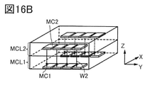
図6Bでは、図6Aに図示する半導体装置10において、Nを6とした場合の各構成の位置関係を説明するための図である。
FIG. 6B is a diagram for explaining the positional relationship of each configuration when N is 6 in the semiconductor device 10 shown in FIG. 6A.
OSトランジスタで構成されるメモリ回路部20_1乃至20_6と、演算回路30_1乃至30_6とは、駆動回路50、切替回路40および演算回路30_1乃至30_6が設けられる基板表面に対して概略垂直な方向に延在して設けられる配線LBL_1乃至LBL_6を介して電気的に接続される。なお「概略垂直」とは、85度以上95度以下の角度で配置されている状態をいう。なお本明細書において図6B等に図示するX方向、Y方向、およびZ方向は、それぞれが互いに直交または交差する方向である。また、X方向およびY方向は基板面に対して平行または概略平行であり、Z方向は基板面に対して垂直または概略垂直である。
The memory circuit units 20_1 to 20_1 composed of OS transistors and the arithmetic circuits 30_1 to 30_6 extend in a direction substantially perpendicular to the surface of the substrate on which the drive circuit 50, the switching circuit 40, and the arithmetic circuits 30_1 to 30_1 are provided. It is electrically connected via the wirings LBL_1 to LBL_1 provided therein. The term "approximately vertical" means a state in which the particles are arranged at an angle of 85 degrees or more and 95 degrees or less. In the present specification, the X direction, the Y direction, and the Z direction shown in FIG. 6B and the like are directions orthogonal to or intersecting each other. Further, the X direction and the Y direction are parallel or substantially parallel to the substrate surface, and the Z direction is perpendicular or substantially perpendicular to the substrate surface.
メモリ回路部20_1乃至20_6はそれぞれ、メモリ回路21を有する。メモリ回路部20_1乃至20_6は、デバイスメモリ、共有メモリという場合がある。メモリ回路21は、トランジスタ22を有する。トランジスタ22が有する半導体層23は、酸化物半導体(金属酸化物)とすることで、上述したOSトランジスタで構成されるメモリ回路21とすることができる。
The memory circuit units 20_1 to 20_1 each have a memory circuit 21. The memory circuit units 20_1 to 20_1 may be referred to as a device memory or a shared memory. The memory circuit 21 has a transistor 22. By using an oxide semiconductor (metal oxide) as the semiconductor layer 23 of the transistor 22, the memory circuit 21 composed of the OS transistor described above can be used.
メモリ回路部20_1乃至20_6が有する複数のメモリ回路21はそれぞれ、配線LBL_1乃至LBL_6に接続される。配線LBL_1乃至LBL_6は、z方向に延びる配線を経由して、切替回路40に接続される。切替回路40は、配線LBL_1乃至LBL_6のいずれか一の電位を増幅して配線GBLに伝える構成とする。当該構成とすることで、切替回路40を制御することで配線GBLに与える重みデータを高速で切り替えることができる。
The plurality of memory circuits 21 included in the memory circuit units 20_1 to 20_1 are connected to the wirings LBL_1 to LBL_1, respectively. The wirings LBL_1 to LBL_6 are connected to the switching circuit 40 via the wiring extending in the z direction. The switching circuit 40 is configured to amplify the potential of any one of the wirings LBL_1 to LBL_6 and transmit it to the wiring GBL. With this configuration, the weight data given to the wiring GBL can be switched at high speed by controlling the switching circuit 40.
演算回路30_1乃至30_6は、配線GBLを介して入力される重みデータと、駆動回路50から入力データ線を介して与えられる入力データAINと、に基づいて演算を行う。重みデータを保持するメモリ回路部20_1乃至20_6は、上層に配置することができるため、演算回路30_1乃至30_6を効率的に配置することができる。そのため、駆動回路50から延びる入力データ線を短くすることができ、半導体装置10の低消費電力化および高速化を図ることができる。
The calculation circuits 30_1 to 30_1 perform a calculation based on the weight data input via the wiring GBL and the input data A IN given from the drive circuit 50 via the input data line. Since the memory circuit units 20_1 to 20_1 for holding the weight data can be arranged in the upper layer, the arithmetic circuits 30_1 to 30_1 can be efficiently arranged. Therefore, the input data line extending from the drive circuit 50 can be shortened, and the power consumption and speed of the semiconductor device 10 can be reduced.
次いで図6Bの構成とすることによる利点について説明する。図7Aでは、説明のため、図6Bの各構成をブロック図で示したものである。なお6個のメモリ回路部20_1乃至20_6にあるメモリ回路21から重みデータW1乃至W6が配線LBL_1乃至LBL_6に読み出されるとして説明する。また切替回路40は、配線LBL_1乃至LBL_6に接続される切替回路40_1乃至40_6として説明する。また切替回路40で重みデータW1乃至W6から選択され、配線GBLに与えられる重みデータを重みデータWSELとして説明する。演算回路30_1乃至30_6にはそれぞれ入力データA1乃至A6が与えられ、出力データMAC1乃至MAC6を得るものとして説明する。
Next, the advantages of the configuration shown in FIG. 6B will be described. In FIG. 7A, for the sake of explanation, each configuration of FIG. 6B is shown as a block diagram. It will be described that the weight data W1 to W6 are read out from the memory circuits 21 in the six memory circuit units 20_1 to 20_1 to the wirings LBL_1 to LBL_1. Further, the switching circuit 40 will be described as switching circuits 40_1 to 40_1 connected to the wirings LBL_1 to LBL_1. Further, the weight data selected from the weight data W1 to W6 in the switching circuit 40 and given to the wiring GBL will be described as the weight data W SEL . Input data A 1 to A 6 are given to the arithmetic circuits 30_1 to 30_1, respectively, and the output data MAC 1 to MAC 6 will be obtained.
配線LBL_1乃至LBL_6における上層と下層をつなぐ垂直方向に延びる配線LBLPは、水平方向に延びる配線と比べて短い。そのため、配線LBL_1乃至LBL_6の寄生容量を小さくでき、配線の充放電に要する電荷を削減でき、低消費電力化および演算効率の向上を図ることができる。また、メモリ回路21から配線LBL_1乃至LBL_6への読み出しを高速にできる。
The wiring LBL P extending in the vertical direction connecting the upper layer and the lower layer in the wirings LBL_1 to LBL_1 is shorter than the wiring extending in the horizontal direction. Therefore, the parasitic capacitance of the wirings LBL_1 to LBL_1 can be reduced, the charge required for charging and discharging the wiring can be reduced, the power consumption can be reduced, and the calculation efficiency can be improved. Further, reading from the memory circuit 21 to the wirings LBL_1 to LBL_1 can be performed at high speed.
配線GBLを介して、演算回路30_1乃至30_6では同じ重みデータを用いた演算処理を行うことができる。当該構成は、同じ重みデータを用いた演算処理を行う畳み込みニューラルネットワークの演算処理に適している。
The arithmetic circuits 30_1 to 30_1 can perform arithmetic processing using the same weight data via the wiring GBL. This configuration is suitable for arithmetic processing of a convolutional neural network that performs arithmetic processing using the same weight data.
図7Bは、図7Aに図示する切替回路40に適用可能な回路構成の一例である。図7Bに図示するスリーステートバッファは、配線LBLの電位を制御信号ENに応じて配線GBLに増幅して伝える機能を有する。切替回路40は、マルチプレクサと見做すことができる。複数の入力信号から、1つを選択する機能を有する。
FIG. 7B is an example of a circuit configuration applicable to the switching circuit 40 illustrated in FIG. 7A. The three-state buffer illustrated in FIG. 7B has a function of amplifying and transmitting the potential of the wiring LBL to the wiring GBL in response to the control signal EN. The switching circuit 40 can be regarded as a multiplexer. It has a function to select one from a plurality of input signals.
図8では、図7Aで説明した構成の動作を説明するためのタイミングチャートを示す。半導体装置10では、クロック信号CLKのトグル動作(例えば時刻T1乃至T7)に応じて演算処理を行う。クロック信号CLKの周波数を高める構成とすることで、演算処理の高速化を図ることができる。
FIG. 8 shows a timing chart for explaining the operation of the configuration described with reference to FIG. 7A. The semiconductor device 10 performs arithmetic processing according to the toggle operation of the clock signal CLK (for example, times T1 to T7). By increasing the frequency of the clock signal CLK, it is possible to speed up the arithmetic processing.
入力データA1乃至A6をそれぞれ図示するようにA1a乃至A111、A2a乃至A211、A3a乃至A311、A4a乃至A411、A5a乃至A511、A6a乃至A611とクロック信号CLKに応じて高速で切り替える場合、重みデータを与える配線GBLのデータを高速で切り替える必要がある。
As shown in the illustration of the input data A 1 to A 6 , A 1 a to A 1 11, A 2 a to A 2 11, A 3 a to A 3 11, A 4 a to A 4 11, A 5 a to A. When switching between 5 11, A 6 a to A 6 11 at high speed according to the clock signal CLK, it is necessary to switch the data of the wiring GBL that gives weight data at high speed.
本発明の一態様の構成では、切替回路40で配線LBLから配線GBLに選択される重みデータをあらかじめ、配線LBL_1乃至LBL_6に読み出しておく構成とすることで、重みデータを与える配線GBLのデータを高速で切り替えることができる。例えば時刻T1で配線LBL_1に重みデータW1を読出しておき、時刻T6で切替回路40を切り替えて配線LBL_1から配線GBLに重みデータW1を出力する構成とすることができる。時刻T2乃至T7、および時刻T7以降においても、配線LBLへの重みデータの読出しと、配線GBLでの重みデータの選択と、の時刻を異ならせることで、クロック信号CLKに応じた重みデータの切り替えを行う構成とすることができる。
In the configuration of one aspect of the present invention, the weight data selected from the wiring LBL to the wiring GBL in the switching circuit 40 is read in advance to the wiring LBL_1 to LBL_1, so that the wiring GBL data giving the weight data can be obtained. You can switch at high speed. For example, the weight data W1 may be read into the wiring LBL_1 at the time T1, the switching circuit 40 may be switched at the time T6, and the weight data W1 may be output from the wiring LBL_1 to the wiring GBL. Even after the times T2 to T7 and after the time T7, the weight data is switched according to the clock signal CLK by reading the weight data to the wiring LBL and selecting the weight data in the wiring GBL by different times. Can be configured to perform.
図9Aでは、演算回路の具体的な構成例を示す。図9Aでは、8ビットの重みデータの入力データの積和演算を行うことができる演算回路30の構成例を図示している。図9Aにおいて、乗算回路24、加算回路25およびレジスタ26を図示している。乗算回路24で乗算された16ビットのデータは加算回路25に入力する。加算回路25の出力がレジスタ26に保持され、乗算回路24で乗算されるデータと加算回路25で足しあわされることで積和演算が行われる。レジスタは、クロック信号CLKおよびリセット信号reset_Bによって制御される。なお図中「17+α」における「α」は、乗算データを加算することで生じる桁上がりを示したものである。当該構成とすることで重みデータWSELと入力データAINとの積和演算に相当する出力データMACを得ることができる。
FIG. 9A shows a specific configuration example of the arithmetic circuit. FIG. 9A illustrates a configuration example of a calculation circuit 30 capable of performing a product-sum calculation of input data of 8-bit weight data. In FIG. 9A, the multiplication circuit 24, the addition circuit 25, and the register 26 are illustrated. The 16-bit data multiplied by the multiplication circuit 24 is input to the addition circuit 25. The output of the addition circuit 25 is held in the register 26, and the product-sum operation is performed by adding the data to be multiplied by the multiplication circuit 24 and the addition circuit 25. The register is controlled by the clock signal CLK and the reset signal reset_B. Note that "α" in "17 + α" in the figure indicates a carry generated by adding multiplication data. With this configuration, it is possible to obtain an output data MAC corresponding to the product-sum operation of the weight data W SEL and the input data A IN .
また図9Aでは、8ビットのデータを用いた演算処理を行う構成として説明したが、1ビットのデータを用いた構成にも本発明の一態様は適用可能である。当該構成について図9Aと同様に図9Bに図示する。1ビットのデータの場合、図9Bに図示するように、ビット数に応じた演算処理を行えばよい。
Further, in FIG. 9A, the configuration is described as performing arithmetic processing using 8-bit data, but one aspect of the present invention can also be applied to a configuration using 1-bit data. The configuration is illustrated in FIG. 9B in the same manner as in FIG. 9A. In the case of 1-bit data, as shown in FIG. 9B, arithmetic processing may be performed according to the number of bits.
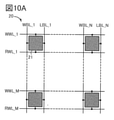
図10Aは、本発明の半導体装置10が有するメモリ回路部20に適用可能な回路構成例について説明する図である。図10Aでは、M行N列(M、Nは2以上の自然数)の行列方向に並べて配置された書込用ワード線WWL_1乃至WWL_M、読出用ワード線RWL_1乃至RWL_M、書込用ビット線WBL_1乃WBL_N、および配線LBL_1乃至LBL_Nを図示している。また各ワード線およびビット線に接続されたメモリ回路21を図示している。
FIG. 10A is a diagram illustrating an example of a circuit configuration applicable to the memory circuit unit 20 included in the semiconductor device 10 of the present invention. In FIG. 10A, writing word lines WWL_1 to WWL_M, reading word lines RWL_1 to RWL_M, and writing bit lines WBL_1 are arranged side by side in the matrix direction of M rows and N columns (M and N are natural numbers of 2 or more). WBL_N and wiring LBL_1 to LBL_N are illustrated. Further, the memory circuit 21 connected to each word line and bit line is illustrated.
図10Bは、メモリ回路21に適用可能な回路構成例について説明する図である。メモリ回路21は、トランジスタ61、トランジスタ62、トランジスタ63、容量素子64(キャパシタともいう)を有する。
FIG. 10B is a diagram illustrating a circuit configuration example applicable to the memory circuit 21. The memory circuit 21 includes a transistor 61, a transistor 62, a transistor 63, and a capacitive element 64 (also referred to as a capacitor).
トランジスタ61のソースまたはドレインの一方は、書込用ビット線WBLに接続される。トランジスタ61のゲートは、書込用ワード線WWLに接続される。トランジスタ61のソースまたはドレインの他方は、容量素子64の一方の電極およびトランジスタ62のゲートに接続される。トランジスタ62のソースまたはドレインの一方および容量素子64の他方の電極は、固定電位たとえばグラウンド電位を与える配線に接続される。トランジスタ62のソースまたはドレインの他方は、トランジスタ63のソースまたはドレインの一方に接続される。トランジスタ63のゲートは、読出用ワード線RWLに接続される。トランジスタ63のソースまたはドレインの他方は、配線LBLに接続される。配線LBLは切替回路40を介して配線GBLに接続される。配線LBLは、上述したように、演算回路30が設けられる基板表面に対して概略垂直な方向に延在して設けられる配線を介して切替回路40に接続される。
One of the source and drain of the transistor 61 is connected to the writing bit line WBL. The gate of the transistor 61 is connected to the writing word line WWL. The other of the source or drain of the transistor 61 is connected to one electrode of the capacitive element 64 and the gate of the transistor 62. One of the source or drain of the transistor 62 and the other electrode of the capacitive element 64 are connected to a wire that provides a fixed potential, eg, a ground potential. The other of the source or drain of the transistor 62 is connected to one of the source or drain of the transistor 63. The gate of the transistor 63 is connected to the read word line RWL. The other of the source or drain of the transistor 63 is connected to the wiring LBL. The wiring LBL is connected to the wiring GBL via the switching circuit 40. As described above, the wiring LBL is connected to the switching circuit 40 via wiring provided so as to extend in a direction substantially perpendicular to the surface of the substrate on which the arithmetic circuit 30 is provided.
図10Bに示すメモリ回路21の回路構成は、3トランジスタ型(3T)ゲインセルのNOSRAMに相当する。トランジスタ61乃至トランジスタ63は、OSトランジスタである。OSトランジスタはオフ状態でソースとドレインとの間を流れる電流、つまりリーク電流が極めて小さい。NOSRAMは、リーク電流が極めて小さい特性を用いてデータに応じた電荷をメモリ回路内に保持することで、不揮発性メモリとして用いることができる。
The circuit configuration of the memory circuit 21 shown in FIG. 10B corresponds to the NOSRAM of the 3-transistor type (3T) gain cell. The transistor 61 to the transistor 63 are OS transistors. The OS transistor has an extremely small leakage current, that is, a current flowing between the source and the drain in the off state. The NOSRAM can be used as a non-volatile memory by holding a charge corresponding to the data in the memory circuit using the characteristic that the leakage current is extremely small.
図10Aのメモリ回路21に適用可能な回路構成は、図10Bの3T型のNOSRAMに限らない。例えば、図11Aに図示するDOSRAMに相当する回路でもよい。図11Aでは、トランジスタ61Aおよび容量素子64Aを有するメモリ回路21Aを図示している。トランジスタ61Aは、OSトランジスタである。メモリ回路21Aは、ビット線BL、ワード線WLおよびバックゲート線BGLに接続される例を図示している。
The circuit configuration applicable to the memory circuit 21 of FIG. 10A is not limited to the 3T type NOSRAM of FIG. 10B. For example, it may be a circuit corresponding to the DOSRAM shown in FIG. 11A. FIG. 11A illustrates a memory circuit 21A having a transistor 61A and a capacitive element 64A. The transistor 61A is an OS transistor. The memory circuit 21A illustrates an example of being connected to a bit line BL, a word line WL, and a back gate line BGL.
図10Aのメモリ回路21に適用可能な回路構成は、図11Bに図示する2T型のNOSRAMに相当する回路でもよい。図11Bでは、トランジスタ61B、トランジスタ62Bおよび容量素子64Bを有するメモリ回路21Bを図示している。トランジスタ61Bおよびトランジスタ62Bは、OSトランジスタである。トランジスタ61Bおよびトランジスタ62Bは、異なる層に半導体層が配置されるOSトランジスタもよいし、同じ層に半導体層が配置されるOSトランジスタでもよい。メモリ回路21Bは、書込用ビット線WBL、読出用ビット線RBL、書込用ワード線WWL、読出用ワード線RWL、ソース線SLおよびバックゲート線BGLに接続される例を図示している。
The circuit configuration applicable to the memory circuit 21 of FIG. 10A may be a circuit corresponding to the 2T type NOSRAM shown in FIG. 11B. FIG. 11B illustrates a memory circuit 21B having a transistor 61B, a transistor 62B, and a capacitive element 64B. The transistor 61B and the transistor 62B are OS transistors. The transistor 61B and the transistor 62B may be an OS transistor in which a semiconductor layer is arranged in different layers, or an OS transistor in which a semiconductor layer is arranged in the same layer. The memory circuit 21B illustrates an example of being connected to a write bit line WBL, a read bit line RBL, a write word line WWL, a read word line RWL, a source line SL, and a backgate line BGL.
図10Aのメモリ回路21に適用可能な回路構成は、図11Cに図示する3T型のNOSRAMを組み合わせた回路でもよい。図11Cでは、論理の異なるデータを保持できるメモリ回路21_Pと、メモリ回路21_Nと、を有するメモリ回路21Cを図示している。図11Cでは、トランジスタ61_P、トランジスタ62_P、トランジスタ63_Pおよび容量素子64_Pを有するメモリ回路21_Pと、トランジスタ61_N、トランジスタ62_N、トランジスタ63_Nおよび容量素子64_Nを有するメモリ回路21_Nと、を図示している。メモリ回路21_Pおよびメモリ回路21_Nが有する各トランジスタは、OSトランジスタである。メモリ回路21_Pおよびメモリ回路21_Nが有する各トランジスタは、異なる層に半導体層が配置されるOSトランジスタもよいし、同じ層に半導体層が配置されるOSトランジスタでもよい。メモリ回路21Cは、書込用ビット線WBL_P、配線LBL_P、書込用ビット線WBL_N、配線LBL_N、書込用ワード線WWL、読出用ワード線RWLに接続される例を図示している。メモリ回路21Cは、論理の異なるデータを保持し、論理の異なるデータを配線LBL_Pおよび配線LBL_Nに読出し、図7などと同様に、切替回路40を介して配線GBL_Pおよび配線GBL_Nに出力することができる。
The circuit configuration applicable to the memory circuit 21 of FIG. 10A may be a circuit in which the 3T type NOSRAM shown in FIG. 11C is combined. FIG. 11C illustrates a memory circuit 21C having a memory circuit 21_P capable of holding data having different logics and a memory circuit 21_N. FIG. 11C illustrates a memory circuit 21_P having a transistor 61_P, a transistor 62_P, a transistor 63_P and a capacitive element 64_P, and a memory circuit 21_N having a transistor 61_N, a transistor 62_N, a transistor 63_N and a capacitive element 64_N. Each transistor included in the memory circuit 21_P and the memory circuit 21_N is an OS transistor. Each transistor included in the memory circuit 21_P and the memory circuit 21_N may be an OS transistor in which a semiconductor layer is arranged in different layers, or an OS transistor in which a semiconductor layer is arranged in the same layer. The memory circuit 21C shows an example of being connected to a writing bit line WBL_P, a wiring LBL_P, a writing bit line WBL_N, a wiring LBL_N, a writing word line WWL, and a reading word line RWL. The memory circuit 21C holds data having different logics, reads data having different logics to the wiring LBL_P and the wiring LBL_N, and can output the data to the wiring GBL_P and the wiring GBL_N via the switching circuit 40 in the same manner as in FIG. ..
なお図11Cの構成において、メモリ回路21_Pと、メモリ回路21_Nとに保持するデータの乗算に相当するデータが配線LBLに出力されるように排他的論理和回路(XOR回路)を設けてもよい。当該構成とすることで、演算回路30における乗算に相当する演算を省略できるため、低消費電力化を図ることができる。
In the configuration of FIG. 11C, an exclusive OR circuit (XOR circuit) may be provided so that the data corresponding to the multiplication of the data held in the memory circuit 21_P and the memory circuit 21_N is output to the wiring LBL. With this configuration, the calculation corresponding to the multiplication in the calculation circuit 30 can be omitted, so that the power consumption can be reduced.
図12には、畳み込みニューラルネットワークの演算処理の流れを図示する。図12では、入力層90A、中間層90B(隠れ層ともいう)、出力層90Cを図示している。入力層90Aでは、入力データの入力処理91(図中、Inputと図示)を図示している。中間層90Bでは、畳み込み演算処理92、93、95(図中、Conv.と図示)、複数のプーリング演算処理94、96(図中、Pool.と図示)を図示している。出力層90Cでは、全結合演算処理97(図中、Fullと図示)を図示している。入力層90A、中間層90B、出力層90Cにおける演算処理の流れは一例であり、実際の畳み込みニューラルネットワークの演算処理では、ソフトマックス演算などの他の演算処理を行うことがあり得る。
FIG. 12 illustrates the flow of arithmetic processing of a convolutional neural network. FIG. 12 illustrates an input layer 90A, an intermediate layer 90B (also referred to as a hidden layer), and an output layer 90C. The input layer 90A illustrates an input data input process 91 (shown as Input in the figure). In the intermediate layer 90B, convolution calculation processes 92, 93, 95 (shown as Conv. In the figure) and a plurality of pooling calculation processes 94, 96 (shown as Pool. In the figure) are illustrated. In the output layer 90C, the fully combined operation process 97 (shown as Full in the figure) is illustrated. The flow of arithmetic processing in the input layer 90A, the intermediate layer 90B, and the output layer 90C is an example, and in the actual arithmetic processing of the convolutional neural network, other arithmetic processing such as softmax arithmetic may be performed.
図12に図示する畳み込みニューラルネットワークでは、図12に図示するように、複数回の畳み込み演算処理92、93、95を行う。畳み込み演算処理では、同じ重みデータを用いた演算処理を行う。そのため、同じ重みデータを用いる演算処理を行う本実施の一態様の構成を適用することで動作速度と、低消費電力化との両立を図ることができる。
In the convolutional neural network shown in FIG. 12, as shown in FIG. 12, the convolutional operation processes 92, 93, and 95 are performed a plurality of times. In the convolution operation process, the operation process using the same weight data is performed. Therefore, by applying the configuration of one aspect of the present embodiment in which the arithmetic processing using the same weight data is performed, it is possible to achieve both the operating speed and the low power consumption.
また、先の実施の形態で示したように、全結合演算処理97については、アナログ演算器102および酸化物半導体メモリ104を用いて演算することが好ましい。アナログ演算器102および酸化物半導体メモリ104はサブスレッショルド領域で駆動させることができるので、低消費電力化を図ることができる。
Further, as shown in the previous embodiment, it is preferable that the fully coupled arithmetic processing 97 is calculated by using the analog arithmetic unit 102 and the oxide semiconductor memory 104. Since the analog arithmetic unit 102 and the oxide semiconductor memory 104 can be driven in the sub-threshold region, low power consumption can be achieved.
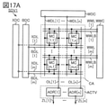
次に、半導体装置10の詳細なブロック図について図13に示す。
Next, FIG. 13 shows a detailed block diagram of the semiconductor device 10.
図13では、図5Aおよび図5B、並びに図6Aおよび図6Bで説明した、メモリ回路部20、メモリ回路21、演算回路30、切替回路40、層11、層12に相当する構成の他、図6Aおよび図6Bで図示する駆動回路50の構成例について図示している。
In FIG. 13, in addition to the configurations corresponding to the memory circuit unit 20, the memory circuit 21, the arithmetic circuit 30, the switching circuit 40, the layer 11, and the layer 12, which are described in FIGS. 5A and 5B, and FIGS. The configuration example of the drive circuit 50 shown in 6A and 6B is illustrated.
図13では、図6Aおよび図6Bで説明した駆動回路50に対応する構成として、コントローラ71、ロウデコーダ72、ワード線ドライバ73、カラムデコーダ74、書き込みドライバ75、プリチャージ回路76、入出力バッファ81および演算制御回路82を図示している。
In FIG. 13, the controller 71, the row decoder 72, the word line driver 73, the column decoder 74, the write driver 75, the precharge circuit 76, and the input / output buffer 81 are configured to correspond to the drive circuit 50 described with reference to FIGS. 6A and 6B. And the arithmetic control circuit 82 is illustrated.
図14Aは、図13に図示する各構成について、メモリ回路部20を制御するブロックを抜き出した図である。図14Aでは、コントローラ71、ロウデコーダ72、ワード線ドライバ73、カラムデコーダ74、書き込みドライバ75、プリチャージ回路76を抜き出して図示している。
FIG. 14A is a diagram in which a block that controls the memory circuit unit 20 is extracted for each configuration shown in FIG. In FIG. 14A, the controller 71, the row decoder 72, the word line driver 73, the column decoder 74, the write driver 75, and the precharge circuit 76 are extracted and shown.
コントローラ71は、外部からの入力信号を処理して、ロウデコーダ72およびカラムデコーダ74の制御信号を生成する。外部からの入力信号は、書き込みイネーブル信号及び読み出しイネーブル信号などのメモリ回路部20を制御するための制御信号である。またコントローラ71は、CPU110と半導体装置10の間でバス120を介してデータの入出力が行われる。
The controller 71 processes an input signal from the outside to generate a control signal for the row decoder 72 and the column decoder 74. The input signal from the outside is a control signal for controlling the memory circuit unit 20 such as a write enable signal and a read enable signal. Further, the controller 71 inputs / outputs data between the CPU 110 and the semiconductor device 10 via the bus 120.
ロウデコーダ72は、ワード線ドライバ73を駆動するための信号を生成する。ワード線ドライバ73は、書込み用ワード線WWL、および読出用ワード線RWLに与える信号を生成する。カラムデコーダ74は、書き込みドライバ75を駆動するための信号を生成する。書き込みドライバ75は、メモリ回路21に与える重みデータを生成する。プリチャージ回路76は、配線LBLなどをプリチャージする機能を有する。メモリ回路部20のメモリ回路21から読み出される重みデータに応じた信号は、図6Aおよび図6B等で説明したように、配線LBLを介して切替回路40に入力される。
The row decoder 72 generates a signal for driving the word line driver 73. The word line driver 73 generates a signal to be given to the writing word line WWL and the reading word line RWL. The column decoder 74 generates a signal for driving the write driver 75. The write driver 75 generates weight data to be given to the memory circuit 21. The precharge circuit 76 has a function of precharging the wiring LBL and the like. The signal corresponding to the weight data read from the memory circuit 21 of the memory circuit unit 20 is input to the switching circuit 40 via the wiring LBL as described with reference to FIGS. 6A and 6B.
図14Bは、図13に図示する各構成について、演算回路30および切替回路40を制御するブロックを抜き出した図である。
FIG. 14B is a diagram in which blocks for controlling the arithmetic circuit 30 and the switching circuit 40 are extracted for each configuration shown in FIG.
コントローラ71は、外部からの入力信号を処理して、演算制御回路82の制御信号を生成する。またコントローラ71は、演算回路30を制御するためのアドレス信号、およびクロック信号などの各種信号を生成する。演算制御回路82は、コントローラ71の制御および入出力バッファ81の出力に応じて、データ入力線に与えられる入力データA1乃至ANを生成する。演算制御回路82は、切替回路40を制御する制御信号を出力する。切替回路40は、図6Aおよび図6B等で説明したように、複数の配線LBLの与えられる重みデータのいずれか一を、配線GBLを介して複数の演算回路30に与える。演算回路30は、与えられる重みデータおよび入力データを切り替えることで、積和演算に応じた出力データMACを生成する。生成された出力データMACは、中間データとして入出力バッファ81を介して演算制御回路82内のSRAMあるいはレジスタなどのメモリに一時的に保持される。保持された中間データは、演算回路30に再入力される。
The controller 71 processes an input signal from the outside to generate a control signal of the arithmetic control circuit 82. Further, the controller 71 generates various signals such as an address signal for controlling the arithmetic circuit 30 and a clock signal. The arithmetic control circuit 82 generates input data A 1 to AN given to the data input line according to the control of the controller 71 and the output of the input / output buffer 81. The arithmetic control circuit 82 outputs a control signal for controlling the switching circuit 40. As described with reference to FIGS. 6A and 6B, the switching circuit 40 gives any one of the weight data given by the plurality of wiring LBLs to the plurality of arithmetic circuits 30 via the wiring GBL. The arithmetic circuit 30 generates an output data MAC corresponding to the product-sum operation by switching between the given weight data and the input data. The generated output data MAC is temporarily held as intermediate data in a memory such as an SRAM or a register in the arithmetic control circuit 82 via the input / output buffer 81. The retained intermediate data is re-input to the arithmetic circuit 30.
なお本発明の一態様における半導体装置10は、並列数が高められた並列計算を可能にするため、複数組み合わせて用いる構成が好ましい。この場合の構成例について図15A、図15Bを用いて説明する。
The semiconductor device 10 according to one aspect of the present invention is preferably configured to be used in combination of a plurality of semiconductor devices 10 in order to enable parallel calculation with an increased number of parallel processes. A configuration example in this case will be described with reference to FIGS. 15A and 15B.
図15Aでは、上述した半導体装置10に対応する構成として、半導体装置10_1乃至10_n(nは2以上の数)と、半導体装置10_1乃至10_nとの間でデータの入出力および制御を行うコントローラ71Gを図示している。コントローラ71Gは、内部にSRAM等のメモリ回路60を有する。コントローラ71Gは、複数の半導体装置10_1乃至10_nで得られる出力データMACをメモリ回路60に保持する。そしてメモリ回路60に保持した出力データMACを複数の半導体装置10_1乃至10_nにおける入力データAINとして出力する構成とする。当該構成とすることで複数の半導体装置を用いた、並列数が高められた並列計算を行うことができる。
In FIG. 15A, as a configuration corresponding to the above-mentioned semiconductor device 10, a controller 71G that inputs / outputs and controls data between the semiconductor devices 10_1 to 10_n (n is a number of 2 or more) and the semiconductor devices 10_1 to 10_n is provided. It is shown in the figure. The controller 71G has a memory circuit 60 such as an SRAM inside. The controller 71G holds the output data MAC obtained by the plurality of semiconductor devices 10_1 to 10_n in the memory circuit 60. Then, the output data MAC held in the memory circuit 60 is output as input data A IN in the plurality of semiconductor devices 10_1 to 10_n. With this configuration, it is possible to perform parallel calculation with an increased number of parallels using a plurality of semiconductor devices.
また図15Aとは別の構成例である図15Bでは、コントローラ71Gにおいて、メモリ回路60に保持した出力データに対し、別の演算処理を施した入力データを複数の半導体装置10_1乃至10_nにおける入力データAIN_1乃至AIN_nをとして出力する構成とする。当該構成の場合、例えばコントローラ71Gでは、メモリ回路60に保持した出力データに対し、活性化関数に基づく演算処理、プーリング処理、規格化演算処理(ノーマライゼーション)などを行う構成とする。当該構成とすることで複数の半導体装置を用いた、並列数が高められた並列計算に加え、畳み込み演算処理以外の演算処理を効率よく行うことができる。
Further, in FIG. 15B, which is a configuration example different from that of FIG. 15A, the input data obtained by subjecting the output data held in the memory circuit 60 to the output data held in the memory circuit 60 in the controller 71G is input data in the plurality of semiconductor devices 10_1 to 10_n. The configuration is such that A IN _1 to A IN _n are output as. In the case of this configuration, for example, the controller 71G is configured to perform arithmetic processing, pooling processing, normalization arithmetic processing (normalization), etc. based on the activation function on the output data held in the memory circuit 60. With this configuration, in addition to parallel calculation with an increased number of parallels using a plurality of semiconductor devices, it is possible to efficiently perform arithmetic processing other than convolution arithmetic processing.
半導体装置10では、入出力バッファ81におけるバッファメモリを利用して演算回路30の演算結果に応じた出力データMACを中間データとして演算制御回路82に入力する。演算制御回路82がこの中間データを再度演算回路30への入力データとして出力できる。そのため、演算途中のデータを半導体装置10の外部にあるメインメモリなどに読み出すことなく、演算処理を実行可能である。また半導体装置10では、メモリ回路部と、演算回路と、の間の電気的な接続を、絶縁膜等に設ける開口部の配線を介して行うことができるため、配線数をふやすことで並列数を増やすことが可能である。そのため半導体装置10では、CPU110のデータバス幅以上のビット数の並列計算が可能となる。また膨大な数の重みデータをCPU110との間で転送する回数を削減できるため、低消費電力化を図ることができる。
In the semiconductor device 10, the output data MAC corresponding to the calculation result of the calculation circuit 30 is input to the calculation control circuit 82 as intermediate data by using the buffer memory in the input / output buffer 81. The arithmetic control circuit 82 can output this intermediate data again as input data to the arithmetic circuit 30. Therefore, the calculation process can be executed without reading the data in the middle of the calculation to the main memory or the like outside the semiconductor device 10. Further, in the semiconductor device 10, since the electrical connection between the memory circuit portion and the arithmetic circuit can be made via the wiring of the opening provided in the insulating film or the like, the number of parallels can be increased by increasing the number of wirings. It is possible to increase. Therefore, in the semiconductor device 10, parallel calculation of the number of bits equal to or larger than the data bus width of the CPU 110 is possible. Further, since the number of times that a huge amount of weight data is transferred to and from the CPU 110 can be reduced, it is possible to reduce the power consumption.
以上説明したように、本発明の一態様は、小型化が図られた、アクセラレータとして機能する半導体装置を提供することができる。または、本発明の一態様は、演算処理速度の向上が図られた、アクセラレータとして機能する半導体装置を提供することができる。または、本発明の一態様は、演算精度の向上が図られた、アクセラレータとして機能する半導体装置を提供することができる。または、本発明の一態様は、低消費電力化が図られた、アクセラレータとして機能する半導体装置を提供することができる。または、新規な構成の、アクセラレータとして機能する半導体装置を提供することができる。
As described above, one aspect of the present invention can provide a semiconductor device that functions as an accelerator and is miniaturized. Alternatively, one aspect of the present invention can provide a semiconductor device that functions as an accelerator with improved arithmetic processing speed. Alternatively, one aspect of the present invention can provide a semiconductor device that functions as an accelerator with improved calculation accuracy. Alternatively, one aspect of the present invention can provide a semiconductor device that functions as an accelerator with low power consumption. Alternatively, it is possible to provide a semiconductor device having a new configuration and functioning as an accelerator.
なお、本実施の形態は、本明細書で示す他の実施の形態と適宜組み合わせることができる。
It should be noted that this embodiment can be appropriately combined with other embodiments shown in the present specification.
(実施の形態3)
本実施の形態では、先の実施の形態に示す半導体装置100の一部の構成、および動作等について説明する。本実施の形態に示す半導体装置は、半導体装置100の一部であり、先の実施の形態に示す、アナログ演算器102と酸化物半導体メモリ104を有する。
(Embodiment 3)
In this embodiment, a configuration, operation, and the like of a part of the semiconductor device 100 shown in the previous embodiment will be described. The semiconductor device shown in this embodiment is a part of the semiconductor device 100, and has the analog arithmetic unit 102 and the oxide semiconductor memory 104 shown in the previous embodiment.
<構成例>
図16Aおよび図16Bは、本発明の一態様の半導体装置である、乗算セルの構成例について示している。当該乗算セルは、一例として、トランスリニア原理を用いて乗算を行う構成となっている。また、当該乗算セルは、一例として、第1データを保持する機能を有し、また、当該乗算セルに第2データが入力されることによって、第1データと第2データの積を出力する機能を有する。ここで、第1データは図1Bに示す重みデータW2に対応し、第2データは図1Bに示す入力データA2に対応する。
<Configuration example>
16A and 16B show a configuration example of a multiplication cell, which is a semiconductor device according to one aspect of the present invention. As an example, the multiplication cell is configured to perform multiplication using the translinear principle. Further, the multiplication cell has a function of holding the first data as an example, and a function of outputting the product of the first data and the second data by inputting the second data to the multiplication cell. Have. Here, the first data corresponds to the weight data W2 shown in FIG. 1B, and the second data corresponds to the input data A2 shown in FIG. 1B.
図16Aに示す回路MCは、トランジスタM1乃至トランジスタM10と、容量C1と、容量CGと、を有する。回路MCは、トランジスタM5乃至トランジスタM10を有する回路MC1と、トランジスタM1乃至トランジスタM4、および容量C1を有する回路MC2と、に機能的に分けることができる。ここで、回路MC1は先の実施の形態に示すアナログ演算器102に対応し、回路MC2は先の実施の形態に示す酸化物半導体メモリ104に対応する。
The circuit MC shown in FIG. 16A has transistors M1 to M10, a capacitance C1, and a capacitance CG. The circuit MC can be functionally divided into a circuit MC1 having transistors M5 to M10, and a circuit MC2 having transistors M1 to M4 and a capacitance C1. Here, the circuit MC1 corresponds to the analog arithmetic unit 102 shown in the previous embodiment, and the circuit MC2 corresponds to the oxide semiconductor memory 104 shown in the previous embodiment.
回路MC1および回路MC2は、図2Aおよび図2Bで示した、アナログ演算器102および酸化物半導体メモリ104と同様に同一の層に設けることができる。図2Aおよび図2Bでは、アナログ演算器102の領域と、酸化物半導体メモリ104の領域を分けて示したが、これに限られることなく、回路MC1と回路MC2を一つにまとめた回路MCをアレイ状に設ける構成にしてもよい。
The circuit MC1 and the circuit MC2 can be provided on the same layer as the analog arithmetic unit 102 and the oxide semiconductor memory 104 shown in FIGS. 2A and 2B. In FIGS. 2A and 2B, the area of the analog arithmetic unit 102 and the area of the oxide semiconductor memory 104 are shown separately, but the circuit MC1 and the circuit MC2 are combined into one without being limited to this. It may be configured to be provided in an array.
回路MCをアレイ状に設ける場合、図16Bに示すように、回路MC1を、図中xy平面にトランジスタを有する層MCL1に設け、回路MC2を、図中xy平面にトランジスタを有する層MCL2に設ける構成にしてもよい。層MCL1および層MCL2は、チャネル形成領域に酸化物半導体を有するトランジスタ(OSトランジスタ)を有する。層MCL1および層MCL2は、xy平面に対して概略垂直な方向(図16B中、z方向)で異なる層に設けられる。このような構成にすることで、図16Bに示すように、回路MC2から回路MC1に重みデータW2を伝達する配線を短くすることができる。これにより、重みデータW2の読み出しの高速化、および読み出しに伴う消費電力の低減を図ることができる。
When the circuit MC is provided in an array, as shown in FIG. 16B, the circuit MC1 is provided on the layer MCL1 having a transistor on the xy plane in the figure, and the circuit MC2 is provided on the layer MCL2 having the transistor on the xy plane in the figure. You may do it. The layer MCL1 and the layer MCL2 have a transistor (OS transistor) having an oxide semiconductor in the channel forming region. The layer MCL1 and the layer MCL2 are provided in different layers in a direction substantially perpendicular to the xy plane (in the z direction in FIG. 16B). With such a configuration, as shown in FIG. 16B, the wiring for transmitting the weight data W2 from the circuit MC2 to the circuit MC1 can be shortened. As a result, it is possible to speed up the reading of the weight data W2 and reduce the power consumption associated with the reading.
トランジスタM1乃至トランジスタM10としては、例えば、OSトランジスタとすることができる。特に、OSトランジスタのチャネル形成領域に含まれる金属酸化物としては、例えば、インジウム、元素Mおよび亜鉛を有するIn−M−Zn酸化物(元素Mは、アルミニウム、ガリウム、イットリウム、錫、銅、バナジウム、ベリリウム、ホウ素、チタン、鉄、ニッケル、ゲルマニウム、ジルコニウム、モリブデン、ランタン、セリウム、ネオジム、ハフニウム、タンタル、タングステン、またはマグネシウムなどから選ばれた一種、または複数種)等とすること好ましい。また、トランジスタM1乃至トランジスタM10としては、例えば、チャネル形成領域にシリコンを有するトランジスタ(Siトランジスタ)を適用してもよい。また、シリコンとしては、例えば、単結晶シリコン、非晶質シリコン(水素化アモルファスシリコンという場合がある)、微結晶シリコン、または多結晶シリコン等を用いることができる。また、OSトランジスタ、Siトランジスタ以外のトランジスタとしては、例えば、Geなどがチャネル形成領域に含まれているトランジスタ、ZnSe、CdS、GaAs、InP、GaN、SiGeなどの化合物半導体がチャネル形成領域に含まれているトランジスタ、カーボンナノチューブがチャネル形成領域に含まれるトランジスタ、有機半導体がチャネル形成領域に含まれるトランジスタ等を用いることができる。
The transistor M1 to the transistor M10 can be, for example, an OS transistor. In particular, examples of the metal oxide contained in the channel forming region of the OS transistor include indium, an In-M-Zn oxide having element M and zinc (element M is aluminum, gallium, yttrium, tin, copper and vanadium). , Berylium, boron, titanium, iron, nickel, germanium, zirconium, molybdenum, lanthanum, cerium, neodymium, hafnium, tantalum, tungsten, magnesium, etc.). Further, as the transistor M1 to the transistor M10, for example, a transistor (Si transistor) having silicon in the channel forming region may be applied. Further, as the silicon, for example, single crystal silicon, amorphous silicon (sometimes referred to as hydride amorphous silicon), microcrystalline silicon, polycrystalline silicon, or the like can be used. Further, as the transistor other than the OS transistor and the Si transistor, for example, a transistor in which Ge and the like are included in the channel forming region, and a compound semiconductor such as ZnSe, CdS, GaAs, InP, GaN, and SiGe are included in the channel forming region. Transistors, transistors in which carbon nanotubes are contained in the channel forming region, transistors in which organic semiconductors are contained in the channel forming region, and the like can be used.
トランジスタM1、トランジスタM3、及びトランジスタM4のそれぞれは、特に断りのない場合は、例えば、スイッチング素子として機能する場合を含むものとする。すなわち、これらのトランジスタのそれぞれのゲート、ソース、及びドレインには、これらのトランジスタがスイッチング素子として動作する範囲での電圧が適切に入力されている場合を含むものとする。ただし、本発明の一態様は、これに限定されない。例えば、これらのトランジスタの少なくとも一は、オン状態のときは飽和領域、又は線形領域で動作することができる。又は、これらのトランジスタに流れる電流量を小さくするために、トランジスタM1、トランジスタM3、及びトランジスタM4の少なくとも一は、サブスレッショルド領域で動作することができる。又は、トランジスタM1、トランジスタM3、及びトランジスタM4の少なくとも一は、線形領域で動作する場合と、飽和領域で動作する場合と、サブスレッショルド領域で動作する場合と、が混在することができる。又は、トランジスタM1、トランジスタM3、及びトランジスタM4の少なくとも一は、線形領域で動作する場合と、飽和領域で動作する場合と、が混在することができ、又は、飽和領域で動作する場合と、サブスレッショルド領域で動作する場合と、が混在することができ、又は、線形領域で動作する場合と、サブスレッショルド領域で動作する場合と、が混在することができる。
Unless otherwise specified, each of the transistor M1, the transistor M3, and the transistor M4 includes, for example, a case where it functions as a switching element. That is, it is assumed that the gate, source, and drain of each of these transistors include a case where a voltage within a range in which these transistors operate as a switching element is appropriately input. However, one aspect of the present invention is not limited to this. For example, at least one of these transistors can operate in a saturated or linear region when in the on state. Alternatively, in order to reduce the amount of current flowing through these transistors, at least one of the transistor M1, the transistor M3, and the transistor M4 can operate in the subthreshold region. Alternatively, at least one of the transistor M1, the transistor M3, and the transistor M4 can be operated in a linear region, an operation in a saturation region, and an operation in a subthreshold region. Alternatively, at least one of the transistor M1, the transistor M3, and the transistor M4 can be mixed in the case of operating in the linear region and in the saturated region, or in the case of operating in the saturated region, and the sub. The case of operating in the threshold region and the case of operating in the linear region can be mixed, and the case of operating in the subthreshold region and the case of operating in the subthreshold region can be mixed.
ところで、本明細書等において、飽和領域とは、ゲート−ソース間電圧がしきい値電圧よりも大きく、かつゲート−ソース間電圧としきい値電圧との差がソース−ドレイン間電圧よりも大きい領域をいう。又は、飽和領域は、ソース−ドレイン間電圧を変化させても、トランジスタのドレイン電流がほぼ変わらない領域をいう。又は、飽和領域は、ドレイン電流は、ゲート−ソース間電圧の2乗に比例する領域をいう。又は、飽和領域とは、前述の各説明の領域をみなせる領域を含むものとする。
By the way, in the present specification and the like, the saturation region is a region where the gate-source voltage is larger than the threshold voltage and the difference between the gate-source voltage and the threshold voltage is larger than the source-drain voltage. To say. Alternatively, the saturation region refers to a region in which the drain current of the transistor does not change even if the source-drain voltage is changed. Alternatively, the saturation region refers to a region in which the drain current is proportional to the square of the gate-source voltage. Alternatively, the saturated region shall include a region that can be regarded as the region described above.
また、本明細書等において、線形領域とは、ゲート−ソース間電圧がしきい値電圧よりも大きく、ゲート−ソース間電圧としきい値電圧との差がソース−ドレイン間電圧よりも小さい領域をいう。又は、線形領域は、チャネル形成領域が抵抗として働き、ソース−ドレイン間電圧の変化によって、トランジスタのドレイン電流が線形的に変化するように振る舞う領域をいう。又は、線形領域とは、前述の各説明の領域をみなせる領域を含むものとする。
Further, in the present specification and the like, the linear region is a region in which the gate-source voltage is larger than the threshold voltage and the difference between the gate-source voltage and the threshold voltage is smaller than the source-drain voltage. Say. Alternatively, the linear region refers to a region in which the channel formation region acts as a resistance and the drain current of the transistor behaves as if it changes linearly due to a change in the source-drain voltage. Alternatively, the linear region shall include a region that can be regarded as the region described above.
また、本明細書などにおいてサブスレッショルド領域とは、トランジスタのゲート電圧(Vg)−ドレイン電流(Id)特性を示すグラフにおいて、ゲート電圧がしきい値電圧よりも低い領域をいう。またはサブスレッショルド領域とは、グラデュアルチャネル近似(ドリフト電流しか考慮しないモデル)から外れた、キャリアの拡散による電流が流れる領域をいう。またはサブスレッショルド領域とは、ゲート電圧の増加に対してドレイン電流が指数関数的に増大する領域をいう。またはサブスレッショルド領域とは、前述の各説明の領域とみなせる領域を含むものとする。
Further, in the present specification and the like, the subthreshold region refers to a region in which the gate voltage is lower than the threshold voltage in the graph showing the gate voltage (Vg) -drain current (Id) characteristics of the transistor. Alternatively, the subthreshold region refers to a region in which a current flows due to carrier diffusion, which deviates from the gradual channel approximation (a model that considers only drift current). Alternatively, the subthreshold region is a region in which the drain current increases exponentially with an increase in the gate voltage. Alternatively, the subthreshold region shall include a region that can be regarded as the region described above.
また、トランジスタがサブスレッショルド領域で動作する際のドレイン電流を、サブスレッショルド電流という。サブスレッショルド電流は、ドレイン電圧によらず、ゲート電圧に対して指数関数的に増大する。サブスレッショルド電流を用いた回路動作では、ドレイン電圧のばらつきの影響を小さくすることができる。
The drain current when the transistor operates in the subthreshold region is called the subthreshold current. The subthreshold current increases exponentially with respect to the gate voltage, regardless of the drain voltage. In the circuit operation using the subthreshold current, the influence of the variation of the drain voltage can be reduced.
OSトランジスタは、1×10⁻²⁰A未満、1×10⁻²²A未満、あるいは1×10⁻²⁴A未満といったチャネル幅1μm当たりのドレイン電流をもつ。またOSトランジスタは、トランジスタのしきい値電圧において、1.0×10⁻⁸A以下、1.0×10⁻¹²A以下、あるいは1.0×10⁻¹⁵A以下といったチャネル幅1μm当たりのドレイン電流が流れる。つまり、OSトランジスタは、サブスレッショルド領域で動作するゲート電圧の範囲を大きくとることができる。具体的には、OSトランジスタのしきい値電圧をVthとしたとき、サブスレッショルド領域では、Vth−1.0V以上Vth以下、またはVth−0.5V以上Vth以下の電圧範囲のゲート電圧を用いた回路動作を行うことができる。
The OS transistor has a drain current per 1 μm of channel width, such as less than 1 × 10 -20 A, less than 1 × 10 -22 A, or less than 1 × 10 -24 A. Further, the OS transistor drains per 1 μm of channel width such as 1.0 × 10 -8 A or less, 1.0 × 10 -12 A or less, or 1.0 × 10 -15 A or less at the threshold voltage of the transistor. Current flows. That is, the OS transistor can take a large range of the gate voltage operating in the subthreshold region. Specifically, when the threshold voltage of the OS transistor is Vth , in the subthreshold region, the voltage range is Vth -1.0V or more and Vth or less, or Vth -0.5V or more and Vth or less. Circuit operation using the gate voltage can be performed.
一方、Siトランジスタでは、オフ電流が大きく、サブスレッショルド領域で動作するゲート電圧の範囲が狭い。サブスレッショルド電流を利用する場合、OSトランジスタは、Siトランジスタよりも広いゲート電圧の範囲で回路動作を行うことができる。OSトランジスタを、電流値の小さいサブスレッショルド領域で駆動させることで、回路MCの消費電力の低減を図ることができる。
On the other hand, with Si transistors, the off-current is large and the range of gate voltage operating in the subthreshold region is narrow. When subthreshold current is used, the OS transistor can operate in a wider gate voltage range than the Si transistor. By driving the OS transistor in the subthreshold region where the current value is small, the power consumption of the circuit MC can be reduced.
なお、本明細書等において、トランジスタのオフ領域とは、ゲート−ソース間電圧がサブスレッショルド領域の電圧よりも低い領域をいう。また、トランジスタのゲート−ソース間電圧がオフ領域であるとき、トランジスタはオフ状態をとるものとする。また、本明細書等において、トランジスタがオフ状態のときに流れる電流をオフ電流、又はリーク電流と記載する。
In the present specification and the like, the off region of the transistor means a region where the gate-source voltage is lower than the voltage in the subthreshold region. Further, when the gate-source voltage of the transistor is in the off region, the transistor shall be in the off state. Further, in the present specification and the like, the current flowing when the transistor is in the off state is described as an off current or a leak current.
また、トランジスタM2、トランジスタM5乃至トランジスタM10のそれぞれは、特に断りのない場合は、サブスレッショルド領域で動作する場合を含むものとする。
Further, unless otherwise specified, each of the transistor M2, the transistor M5 and the transistor M10 shall include the case of operating in the subthreshold region.
トランジスタM1の第1端子は、配線VDEに電気的に接続され、トランジスタM1の第2端子は、トランジスタM2の第1端子に電気的に接続され、トランジスタM1のゲートは、配線WWLBと、容量CGの第1端子と、に電気的に接続されている。また、トランジスタM3の第1端子は、配線WDLに電気的に接続され、トランジスタM3の第2端子は、トランジスタM2のゲートと、容量CGの第2端子と、容量C1の第1端子と、に電気的に接続されている。また、トランジスタM2の第2端子は、トランジスタM4の第1端子と、容量C1の第2端子と、トランジスタM5のゲートと、トランジスタM7の第1端子と、トランジスタM8のゲートと、に電気的に接続されている。また、トランジスタM4の第2端子は、配線VGEに電気的に接続され、トランジスタM4のゲートは、配線WWLに電気的に接続されている。また、トランジスタM5の第1端子は、配線VDEに電気的に接続され、トランジスタM5の第2端子は、トランジスタM6の第1端子と、トランジスタM7のゲートと、に電気的に接続されている。トランジスタM6のゲートは、配線XDLに電気的に接続され、トランジスタM6の第2端子は、配線VGEに電気的に接続されている。また、トランジスタM7の第2端子は、配線VGEに電気的に接続されている。また、トランジスタM8の第1端子は、配線VDEに電気的に接続され、トランジスタM8の第2端子は、トランジスタM9の第1端子と、トランジスタM10のゲートと、に電気的に接続されている。また、トランジスタM9のゲートは、配線BDLに電気的に接続され、トランジスタM9の第2端子は、配線VGEに電気的に接続されている。また、トランジスタM10の第1端子は、配線OLに電気的に接続され、トランジスタM10の第2端子は、配線VGEに電気的に接続されている。
The first terminal of the transistor M1 is electrically connected to the wiring VDE, the second terminal of the transistor M1 is electrically connected to the first terminal of the transistor M2, and the gate of the transistor M1 is the wiring WWLB and the capacitance CG. It is electrically connected to the first terminal of. Further, the first terminal of the transistor M3 is electrically connected to the wiring WDL, and the second terminal of the transistor M3 is connected to the gate of the transistor M2, the second terminal of the capacitance CG, and the first terminal of the capacitance C1. It is electrically connected. Further, the second terminal of the transistor M2 is electrically connected to the first terminal of the transistor M4, the second terminal of the capacitance C1, the gate of the transistor M5, the first terminal of the transistor M7, and the gate of the transistor M8. It is connected. Further, the second terminal of the transistor M4 is electrically connected to the wiring VGE, and the gate of the transistor M4 is electrically connected to the wiring WWL. Further, the first terminal of the transistor M5 is electrically connected to the wiring VDE, and the second terminal of the transistor M5 is electrically connected to the first terminal of the transistor M6 and the gate of the transistor M7. The gate of the transistor M6 is electrically connected to the wiring XDL, and the second terminal of the transistor M6 is electrically connected to the wiring VGE. Further, the second terminal of the transistor M7 is electrically connected to the wiring VGE. Further, the first terminal of the transistor M8 is electrically connected to the wiring VDE, and the second terminal of the transistor M8 is electrically connected to the first terminal of the transistor M9 and the gate of the transistor M10. Further, the gate of the transistor M9 is electrically connected to the wiring BDL, and the second terminal of the transistor M9 is electrically connected to the wiring VGE. Further, the first terminal of the transistor M10 is electrically connected to the wiring OL, and the second terminal of the transistor M10 is electrically connected to the wiring VGE.
配線VDEは、一例として、定電圧を与える配線として機能する。当該定電圧としては、例えば、高電源電圧とすることができる。
The wiring VDE functions as a wiring that gives a constant voltage as an example. The constant voltage may be, for example, a high power supply voltage.
配線VGEは、一例として、定電圧を与える配線として機能する。当該定電圧としては、例えば、低電源電圧、接地電位などとすることができる。
The wiring VGE functions as a wiring that gives a constant voltage as an example. The constant voltage may be, for example, a low power supply voltage, a ground potential, or the like.
配線WWLは、一例として、回路MCに対して、第1データを書き込むための書き込み信号線として機能する。
The wiring WWL functions as a write signal line for writing the first data to the circuit MC as an example.
配線WWLBは、一例として、配線WWLに送信される書き込み信号に対する反転信号を送信する配線として機能する。なお、配線WWLBは、当該反転信号ではなく、可変電位(例えば、高レベル電位、低レベル電位など)を供給する配線としてもよい。
As an example, the wiring WWLB functions as a wiring for transmitting an inverted signal with respect to a write signal transmitted to the wiring WWL. The wiring WWLB may be wiring that supplies a variable potential (for example, high level potential, low level potential, etc.) instead of the inverted signal.
配線WDLは、一例として、回路MCに第1データに応じた電圧を書き込むための書き込みデータ線として機能する。
The wiring WDL functions as a write data line for writing a voltage corresponding to the first data to the circuit MC as an example.
配線XDLは、一例として、回路MCに第2データに応じた電圧を入力するための信号線として機能する。
The wiring XDL functions as a signal line for inputting a voltage corresponding to the second data to the circuit MC as an example.
そのため、配線XDLに電気的に接続されているゲートを有するトランジスタM6は、電流源として機能する。また、上述したとおり、トランジスタM6は、サブスレッショルド領域で動作する場合を含むため、トランジスタM6の第1端子−第2端子間には、サブスレッショルド領域の電流が流れる。
Therefore, the transistor M6 having a gate electrically connected to the wiring XDL functions as a current source. Further, as described above, since the transistor M6 includes the case of operating in the subthreshold region, a current in the subthreshold region flows between the first terminal and the second terminal of the transistor M6.
配線BDLは、一例として、回路MCに、第1データと第2データとの演算結果に応じた電流の量を調整するための電圧を入力する信号線として機能する。
As an example, the wiring BDL functions as a signal line for inputting a voltage for adjusting the amount of current according to the calculation result of the first data and the second data to the circuit MC.
そのため、配線BDLに電気的に接続されているゲートを有するトランジスタM9は、電流源として機能する。また、上述したとおり、トランジスタM9は、サブスレッショルド領域で動作する場合を含むため、トランジスタM9の第1端子−第2端子間には、サブスレッショルド領域の電流が流れる。
Therefore, the transistor M9 having a gate electrically connected to the wiring BDL functions as a current source. Further, as described above, since the transistor M9 includes the case of operating in the subthreshold region, a current in the subthreshold region flows between the first terminal and the second terminal of the transistor M9.
なお、トランジスタM9に流れる電流量としては、例えば、後述する回路ACTVに含まれている関数系に従った演算を行う回路に適用する変数、定数などとすることができる。
The amount of current flowing through the transistor M9 can be, for example, a variable or a constant applied to a circuit that performs an operation according to a function system included in the circuit ACTV described later.
配線OLは、一例として、第1データと、第2データと、の積に応じた電流を出力するための配線として機能する。
The wiring OL functions as a wiring for outputting a current according to the product of the first data and the second data, as an example.
<動作例>
次に、図16Aの回路MCの動作例について説明する。なお、本動作例において、配線VDEが与える電位を高電源電位とし、配線VGEが与える電位を接地電位(VGND)とする。
<Operation example>
Next, an operation example of the circuit MC of FIG. 16A will be described. In this operation example, the potential given by the wiring VDE is a high power supply potential, and the potential given by the wiring VGE is a ground potential (VGND).
<<書き込み動作>>
初めに、回路MCへの第1データを書き込む動作の一例について説明する。
<< Writing operation >>
First, an example of an operation of writing the first data to the circuit MC will be described.
配線WWLには、高レベル電位が入力される。これにより、トランジスタM3と、トランジスタM4と、のそれぞれのゲートには、当該高レベル電位が入力されるため、トランジスタM3とトランジスタM4はオン状態となる。
A high level potential is input to the wiring WWL. As a result, the high level potential is input to the respective gates of the transistor M3 and the transistor M4, so that the transistor M3 and the transistor M4 are turned on.
このとき、トランジスタM4を介して、配線VGEと、容量C1の第2端子(トランジスタM2の第2端子)と、の間は導通状態となるため、容量C1の第2端子(トランジスタM2の第2端子)の電位は、VGNDとなる。
At this time, since the wiring VGE and the second terminal of the capacitance C1 (the second terminal of the transistor M2) are in a conductive state via the transistor M4, the second terminal of the capacitance C1 (the second terminal of the transistor M2) is in a conductive state. The potential of the terminal) is V GND .
また、このとき、トランジスタM3を介して、配線WDLと容量C1の第1端子(容量CGの第2端子、トランジスタM2のゲートなど)の間が導通状態となる。ここで、配線WDLに第1データに応じた信号(以下、電圧VWとする。)を送信することで、容量C1の第1端子(容量CGの第2端子、トランジスタM2のゲートなど)には第1データに応じた電圧VWが書き込まれる。
Further, at this time, the wiring WDL and the first terminal of the capacitance C1 (the second terminal of the capacitance CG, the gate of the transistor M2, etc.) are in a conductive state via the transistor M3. Here, by transmitting a signal corresponding to the first data (hereinafter referred to as voltage V W ) to the wiring WD L, the first terminal of the capacitance C1 (the second terminal of the capacitance CG, the gate of the transistor M2, etc.) The voltage V W corresponding to the first data is written in.
また、配線WWLBには、配線WWLに送信される信号の反転信号が入力される。具体的には、配線WWLBには、低レベル電位が入力される。そのため、トランジスタM1のゲート(容量CGの第1端子)には、当該低レベル電位が印加される。これにより、トランジスタM1は、オフ状態となる。
Further, the inverted signal of the signal transmitted to the wiring WWL is input to the wiring WWLB. Specifically, a low level potential is input to the wiring WWLB. Therefore, the low level potential is applied to the gate of the transistor M1 (the first terminal of the capacitive CG). As a result, the transistor M1 is turned off.
容量C1の第1端子(容量CGの第2端子、トランジスタM2のゲートなど)には電圧VWが書き込まれたあと、配線WWLには、低レベル電位が入力される。これにより、トランジスタM3と、トランジスタM4と、のそれぞれのゲートには、当該低レベル電位が入力されるため、トランジスタM3とトランジスタM4はオフ状態となる。また、これにより、容量C1の第1端子がフローティング状態となるため、容量C1の第1端子−第2端子間の電圧VW−VGNDが保持される。
After the voltage V W is written to the first terminal of the capacitance C1 (the second terminal of the capacitance CG, the gate of the transistor M2, etc.), a low level potential is input to the wiring WWL. As a result, the low level potential is input to the respective gates of the transistor M3 and the transistor M4, so that the transistor M3 and the transistor M4 are turned off. Further, as a result, the first terminal of the capacitance C1 is in a floating state, so that the voltage VW −V GND between the first terminal and the second terminal of the capacitance C1 is maintained.
厳密には、トランジスタM3のゲートに与えられる電位が高レベル電位から低レベル電位に変化するとき、トランジスタM3のゲート−第2端子間の寄生容量によって、容量C1の第1端子に書き込まれている電圧VWが降圧する場合がある。なお、本明細書では、便宜上、トランジスタM3のゲート−第2端子間の寄生容量によって電圧VWから降圧した電圧も第1データに応じた電圧ということができるものとする。図16Aの回路MCには、電圧VWの降圧を防ぐため、容量CGを設けている。トランジスタM3のゲートに与えられる電位が高レベル電位から低レベル電位に変化するとき、つまり、配線WWLが与える電位が高レベル電位から低レベル電位に変化するとき、配線WWLBでは、配線WWLに送信される信号の反転信号が入力されるため、配線WWLBの電位は低レベル電位から高レベル電位に変化する。このとき、容量CGの第1端子の電位は、低レベル電位から高レベル電位まで高くなるため、容量CGの第2端子の電位(容量C1の第1端子、トランジスタM2のゲートなど)は、容量CGの容量結合によって、理想的には、高レベル電位と低レベル電位の電位差だけ昇圧する。ここで、昇圧する電位差を、トランジスタM3のゲート−第2端子間の寄生容量による電圧VWが降圧した電位差と等しくすることで、トランジスタM3をオフ状態にしたときの電圧VWの降圧を防ぐことができる。なお、容量CGの容量結合によって昇圧する電位差を、トランジスタM3のゲート−第2端子間の寄生容量によって降圧する電位差と等しくするための容量CGの構成については、後述する。
Strictly speaking, when the potential given to the gate of the transistor M3 changes from a high level potential to a low level potential, it is written to the first terminal of the capacitance C1 by the parasitic capacitance between the gate of the transistor M3 and the second terminal. The voltage V W may step down. In this specification, for convenience, it is assumed that the voltage stepped down from the voltage VW due to the parasitic capacitance between the gate and the second terminal of the transistor M3 is also the voltage corresponding to the first data. The circuit MC of FIG. 16A is provided with a capacitance CG in order to prevent the voltage V W from being stepped down. When the potential given to the gate of the transistor M3 changes from a high level potential to a low level potential, that is, when the potential given by the wiring WWL changes from a high level potential to a low level potential, the wiring WWLB transmits to the wiring WWL. Since the inverted signal of the signal is input, the potential of the wiring WWLB changes from the low level potential to the high level potential. At this time, since the potential of the first terminal of the capacitance CG increases from the low level potential to the high level potential, the potential of the second terminal of the capacitance CG (the first terminal of the capacitance C1, the gate of the transistor M2, etc.) is the capacitance. Capacitive coupling of CG ideally boosts the potential difference between the high-level potential and the low-level potential. Here, by making the voltage difference to be boosted equal to the potential difference at which the voltage V W due to the parasitic capacitance between the gate and the second terminal of the transistor M3 is stepped down, the step down of the voltage V W when the transistor M3 is turned off is prevented. be able to. The configuration of the capacitive CG for making the potential difference stepped up by the capacitive coupling of the capacitive CG equal to the potential difference stepped down by the parasitic capacitance between the gate and the second terminal of the transistor M3 will be described later.
また、このとき、配線WWLBに、配線WWLに送信される信号の反転信号ではなく、低レベル電位を供給して、トランジスタM1をオフ状態にしてもよい。これにより、回路MCへの第1データの保持と、トランジスタM2の第1端子への高電源電位の供給の停止と、を同時に行うことができる。
Further, at this time, the transistor M1 may be turned off by supplying the wiring WWLB with a low level potential instead of the inverted signal of the signal transmitted to the wiring WWL. As a result, the holding of the first data in the circuit MC and the stop of the supply of the high power supply potential to the first terminal of the transistor M2 can be performed at the same time.
<<乗算動作>>
次に、回路MCにおいて、第1データと第2データとの乗算動作の一例について説明する。
<< Multiplication operation >>
Next, an example of the multiplication operation between the first data and the second data in the circuit MC will be described.
配線WWLBに高レベル電位が入力されることによって、トランジスタM1がオン状態となるため、トランジスタM2の第1端子には高電源電位が入力されて、トランジスタM2の第1端子−第2端子間には、トランジスタM2のゲート−第2端子間の電圧に応じた電流が流れる。また、ここで、トランジスタM2の第1端子−第2端子間に流れる電流の量をIWとする。なお、トランジスタM2がサブスレッショルド領域で動作する場合、IWは、サブスレッショルド領域における電流範囲の電流量となる。
When a high level potential is input to the wiring WWLB, the transistor M1 is turned on. Therefore, a high power supply potential is input to the first terminal of the transistor M2, and a high power potential is input between the first terminal and the second terminal of the transistor M2. In, a current corresponding to the voltage between the gate and the second terminal of the transistor M2 flows. Further, here, the amount of current flowing between the first terminal and the second terminal of the transistor M2 is defined as IW . When the transistor M2 operates in the subthreshold region, IW is a current amount in the current range in the subthreshold region.
また、トランジスタM2の第1端子−第2端子間に流れる電流は、トランジスタM7を介して、配線VGEに流れる。ここで、トランジスタM7もサブスレッショルド領域で動作するものとして、トランジスタM7の第1端子−第2端子間には、電流量IWの電流が流れるものとする。このとき、電流量IWは、下記の式で表すことができる。
Further, the current flowing between the first terminal and the second terminal of the transistor M2 flows to the wiring VGE via the transistor M7. Here, it is assumed that the transistor M7 also operates in the subthreshold region, and a current having a current amount of IW flows between the first terminal and the second terminal of the transistor M7. At this time, the amount of current I W can be expressed by the following equation.
なお、VM7gsは、トランジスタM7のゲート−第2端子間の電圧である。また、I0は、VM7gsが0のときに流れる電流値であって、トランジスタM7のしきい値電圧、温度、デバイス構造などによって決められる。また、Jは、温度、デバイス構造などによって定められる補正係数である。
The VM7gs is a voltage between the gate and the second terminal of the transistor M7. Further, I 0 is a current value that flows when VM7gs is 0, and is determined by the threshold voltage, temperature, device structure, and the like of the transistor M7. Further, J is a correction coefficient determined by the temperature, the device structure, and the like.
また、配線XDLに第2データに応じた電圧としてVXが入力されるものとする。このとき、トランジスタM6のゲート−第2端子間の電圧はVX−VGNDとなり、トランジスタM6の第1端子−第2端子間には、VX−VGNDに応じた電流が流れる。また、ここで、トランジスタM6の第1端子−第2端子間に流れる電流の量をIXとする。なお、トランジスタM6がサブスレッショルド領域で動作する場合、IXは、サブスレッショルド領域における電流範囲の電流量となる。
Further, it is assumed that V X is input to the wiring XDL as a voltage corresponding to the second data. At this time, the voltage between the gate and the second terminal of the transistor M6 becomes V X -V GND , and a current corresponding to V X -V GND flows between the first terminal and the second terminal of the transistor M6. Further, here, the amount of current flowing between the first terminal and the second terminal of the transistor M6 is defined as IX . When the transistor M6 operates in the subthreshold region, IX is a current amount in the current range in the subthreshold region.
また、トランジスタM6の第1端子−第2端子間に流れる電流は、配線VDEから、トランジスタM5を介して、トランジスタM6の第1端子に流れる電流となる。ここで、トランジスタM5もサブスレッショルド領域で動作するものとして、トランジスタM5の第1端子一第2端子間には、電流量IXの電流が流れるものとする。このとき、電流量IXは、下記の式で表すことができる。
Further, the current flowing between the first terminal and the second terminal of the transistor M6 is the current flowing from the wiring VDE to the first terminal of the transistor M6 via the transistor M5. Here, it is assumed that the transistor M5 also operates in the subthreshold region, and a current having a current amount of IX flows between the first terminal and the second terminal of the transistor M5. At this time, the amount of current IX can be expressed by the following equation.
なお、VM5gsは、トランジスタM5のゲート−第2端子間の電圧である。また、I0は、VM5gsが0のときに流れる電流値であって、トランジスタM5のしきい値電圧、温度、デバイス構造などによって決められる。また、Jは、温度、デバイス構造などによって定められる補正係数である。なお、式(1.2)に用いられている、I0及びJのそれぞれは、式(1.1)に用いられているI0及びJと等しいものとする。
The VM5gs is a voltage between the gate and the second terminal of the transistor M5. Further, I 0 is a current value that flows when VM5gs is 0, and is determined by the threshold voltage, temperature, device structure, and the like of the transistor M5. Further, J is a correction coefficient determined by the temperature, the device structure, and the like. It should be noted that each of I 0 and J used in the formula (1.2) shall be equal to I 0 and J used in the formula (1.1).
また、配線BDLに出力電流を調整するための電圧としてVBが入力されるものとする。このとき、トランジスタM9のゲート−第2端子間の電圧はVB−VGNDとなり、トランジスタM9の第1端子−第2端子間には、VB−VGNDに応じた電流が流れる。また、ここで、トランジスタM9の第1端子−第2端子間に流れる電流の量をIBとする。なお、トランジスタM9がサブスレッショルド領域で動作する場合、IBは、サブスレッショルド領域における電流範囲の電流量となる。
Further, it is assumed that V B is input to the wiring BDL as a voltage for adjusting the output current. At this time, the voltage between the gate and the second terminal of the transistor M9 becomes V B − V GND , and a current corresponding to V B − V GND flows between the first terminal and the second terminal of the transistor M9. Further, here, the amount of current flowing between the first terminal and the second terminal of the transistor M9 is defined as IB. When the transistor M9 operates in the subthreshold region, IB is a current amount in the current range in the subthreshold region.
また、トランジスタM9の第1端子−第2端子間に流れる電流は、配線VDEから、トランジスタM8を介して、トランジスタM9の第1端子に流れる電流となる。ここで、トランジスタM8もサブスレッショルド領域で動作するものとして、トランジスタM8の第1端子−第2端子間には、電流量IBの電流が流れるものとする。このとき、電流量IBは、下記の式で表すことができる。
Further, the current flowing between the first terminal and the second terminal of the transistor M9 is the current flowing from the wiring VDE to the first terminal of the transistor M9 via the transistor M8. Here, it is assumed that the transistor M8 also operates in the subthreshold region, and a current having a current amount of IB flows between the first terminal and the second terminal of the transistor M8. At this time, the current amount IB can be expressed by the following equation.
なお、VM8gsは、トランジスタM8のゲート−第2端子間の電圧である。また、I0は、VM8gsが0のときに流れる電流値であって、トランジスタM8のしきい値電圧、温度、デバイス構造などによって決められる。また、Jは、温度、デバイス構造などによって定められる補正係数である。なお、式(1.3)に用いられている、I0及びJのそれぞれは、式(1.1)、及び式(1.2)に用いられているI0及びJと等しいものとする。
The VM8gs is a voltage between the gate and the second terminal of the transistor M8. Further, I 0 is a current value that flows when VM8gs is 0, and is determined by the threshold voltage, temperature, device structure, and the like of the transistor M8. Further, J is a correction coefficient determined by the temperature, the device structure, and the like. It should be noted that each of I 0 and J used in the formula (1.3) shall be equal to I 0 and J used in the formula (1.1) and the formula (1.2). ..
また、トランジスタM10の第1端子−第2端子間に流れる電流は、トランジスタM10のゲート−第2端子間の電圧に応じて決められる。また、トランジスタM10の第1端子−第2端子間に流れる電流量をIYとしたとき、電流量IYは、下記の式で表すことができる。
Further, the current flowing between the first terminal and the second terminal of the transistor M10 is determined according to the voltage between the gate and the second terminal of the transistor M10. Further, when the amount of current flowing between the first terminal and the second terminal of the transistor M10 is YY , the amount of current YY can be expressed by the following equation.
なお、VM10gsは、トランジスタM10のゲート−第2端子間の電圧である。また、I0は、VM10gsが0のときに流れる電流値であって、トランジスタM10のしきい値電圧、温度、デバイス構造などによって決められる。また、Jは、温度、デバイス構造などによって定められる補正係数である。なお、式(1.4)に用いられている、I0及びJのそれぞれは、式(1.1)乃至式(1.3)に用いられているI0及びJと等しいものとする。
The VM10gs is a voltage between the gate and the second terminal of the transistor M10. Further, I 0 is a current value that flows when VM10gs is 0, and is determined by the threshold voltage, temperature, device structure, and the like of the transistor M10. Further, J is a correction coefficient determined by the temperature, the device structure, and the like. It should be noted that each of I 0 and J used in the formula (1.4) shall be equal to I 0 and J used in the formulas (1.1) to (1.3).
ここで、配線VGE、トランジスタM7の第2端子、トランジスタM7のゲート、トランジスタM5の第2端子、トランジスタM5のゲート、トランジスタM8のゲート、トランジスタM8の第2端子、トランジスタM10のゲート、トランジスタM10の第2端子、配線VGEという順の閉回路を考える。当該閉回路では、キルヒホッフの第二法則(電圧則)により、下記の式が成り立つ。
Here, the wiring VGE, the second terminal of the transistor M7, the gate of the transistor M7, the second terminal of the transistor M5, the gate of the transistor M5, the gate of the transistor M8, the second terminal of the transistor M8, the gate of the transistor M10, and the transistor M10. Consider a closed circuit in the order of the second terminal and the wiring VGE. In the closed circuit, the following equation holds according to Kirchhoff's second law (voltage law).
また、式(1.5)の各電圧の項を、式(1.1)乃至式(1.4)を用いて書き直すことにより、次の式が得られる。
Further, by rewriting the terms of each voltage in the equation (1.5) using the equations (1.1) to (1.4), the following equation can be obtained.
つまり、トランジスタM10の第1端子−第2端子間に流れる電流IYは、IWとIXとの積で表すことができる。そのため、配線OLから流れる電流量IYを計測することによって、IWとIXとの積に応じた値を算出することができる。
That is, the current I Y flowing between the first terminal and the second terminal of the transistor M10 can be expressed by the product of I W and IX . Therefore, by measuring the amount of current I Y flowing from the wiring OL, it is possible to calculate a value according to the product of I W and IX .
なお、本発明の一態様の半導体装置に含まれる乗算セルの構成は、図16Aに示す回路MCに限定されない。本発明の一態様の半導体装置に含まれる乗算セルは、状況に応じて、図16Aに示す回路MCを変更した構成とすることができる。
The configuration of the multiplication cell included in the semiconductor device of one aspect of the present invention is not limited to the circuit MC shown in FIG. 16A. The multiplication cell included in the semiconductor device of one aspect of the present invention may have a configuration in which the circuit MC shown in FIG. 16A is modified depending on the situation.
また、図16Aに図示しているトランジスタM1乃至トランジスタM10は、一例としては、チャネルの上下にゲートを有する構造のnチャネル型トランジスタとしており、トランジスタM1乃至トランジスタM10のそれぞれは第1ゲートと第2ゲートとを有する。但し、本明細書等において、便宜上、一例として、第1ゲートをゲート(フロントゲートと記載する場合がある。)、第2ゲートをバックゲートとして区別するように記載しているが、第1ゲートと第2ゲートは互いに入れ替えることができる。そのため、本明細書等において、「ゲート」という語句は「バックゲート」という語句と入れ替えて記載することができる。同様に、「バックゲート」という語句は「ゲート」という語句と入れ替えて記載することができる。具体例としては、「ゲートは第1配線に電気的に接続され、バックゲートは第2配線に電気的に接続されている」という接続構成は、「バックゲートは第1配線に電気的に接続され、ゲートは第2配線に電気的に接続されている」という接続構成として置き換えることができる。
Further, the transistors M1 to M10 shown in FIG. 16A are, for example, n-channel transistors having a structure having gates above and below the channel, and the transistors M1 to M10 are the first gate and the second, respectively. Has a gate. However, in the present specification and the like, for convenience, the first gate is described as a gate (sometimes referred to as a front gate) and the second gate is described as a back gate, but the first gate is described as an example. And the second gate can be interchanged with each other. Therefore, in the present specification and the like, the phrase "gate" can be replaced with the phrase "back gate". Similarly, the phrase "backgate" can be replaced with the phrase "gate". As a specific example, the connection configuration that "the gate is electrically connected to the first wiring and the back gate is electrically connected to the second wiring" is "the back gate is electrically connected to the first wiring". And the gate is electrically connected to the second wiring. "
また、本発明の一態様の半導体装置は、トランジスタのバックゲートの接続構成に依らない。図16Aに図示されているトランジスタM1乃至トランジスタM10には、バックゲートが図示され、当該バックゲートの接続構成については図示されていないが、当該バックゲートの電気的な接続先は、設計の段階で決めることができる。例えば、バックゲートを有するトランジスタにおいて、そのトランジスタのオン電流を高めるために、ゲートとバックゲートとを電気的に接続してもよい。また、例えば、バックゲートを有するトランジスタにおいて、そのトランジスタのしきい値電圧を変動させるため、または、そのトランジスタのオフ電流を小さくするために、外部回路などと電気的に接続されている配線を設けて、当該外部回路などによってトランジスタのバックゲートに固定電位、又は可変電位を与えてもよい。
Further, the semiconductor device of one aspect of the present invention does not depend on the connection configuration of the back gate of the transistor. A back gate is shown in the transistors M1 to M10 shown in FIG. 16A, and the connection configuration of the back gate is not shown. However, the electrical connection destination of the back gate is at the design stage. You can decide. For example, in a transistor having a back gate, the gate and the back gate may be electrically connected in order to increase the on-current of the transistor. Further, for example, in a transistor having a back gate, a wiring electrically connected to an external circuit or the like is provided in order to fluctuate the threshold voltage of the transistor or to reduce the off current of the transistor. Therefore, a fixed potential or a variable potential may be applied to the back gate of the transistor by the external circuit or the like.
<半導体装置の構成例>
ここでは、図16Aに示した回路MCを適用することができる半導体装置の構成例について、説明する。
<Semiconductor device configuration example>
Here, a configuration example of a semiconductor device to which the circuit MC shown in FIG. 16A can be applied will be described.
図17Aは、図16Aの回路MCを適用することができる半導体装置の構成例を示した回路図である。図17Aに示す半導体装置SDV1は、一例として、回路WDCと、回路XDCと、回路BDCと、回路WWCと、セルアレイCAと、回路ACTVと、を有する。また、回路ACTVは、一例として、回路ADR[1]乃至回路ADR[n]を有する。
FIG. 17A is a circuit diagram showing a configuration example of a semiconductor device to which the circuit MC of FIG. 16A can be applied. As an example, the semiconductor device SDV1 shown in FIG. 17A has a circuit WDC, a circuit XDC, a circuit BDC, a circuit WWC, a cell array CA, and a circuit ACTV. Further, the circuit ACTV has a circuit ADR [1] to a circuit ADR [n] as an example.
セルアレイCAは、一例として、図16Aの回路MCを複数有する。具体的には、セルアレイCAにおいて、複数の回路MCは、m行n列(mは1以上の整数であり、nは1以上の整数である。)のマトリクス状に配置されている。図17Aでは、一例として、セルアレイCA内に、回路MCとして、回路MC[1,1]、回路MC[m,1]、回路MC[1,n]、及び回路MC[m,n]を図示している。
As an example, the cell array CA has a plurality of circuit MCs of FIG. 16A. Specifically, in the cell array CA, a plurality of circuits MC are arranged in a matrix of m rows and n columns (m is an integer of 1 or more and n is an integer of 1 or more). In FIG. 17A, as an example, a circuit MC [1,1], a circuit MC [m, 1], a circuit MC [1, n], and a circuit MC [m, n] are shown as circuit MCs in the cell array CA. Shows.
回路MC[1,1]は、配線WDL[1]と、配線WWL[1]と、配線WWLB[1]と、配線XDL[1]と、配線BDL[1]と、配線OL[1]と、に電気的に接続されている。また、回路MC[m,1]は、配線WDL[1]と、配線WWL[m]と、配線WWLB[m]と、配線XDL[m]と、配線BDL[m]と、配線OL[1]と、に電気的に接続されている。また、回路MC[1,n]は、配線WDL[n]と、配線WWL[1]と、配線WWLB[1]と、配線XDL[1]と、配線BDL[1]と、配線OL[n]と、に電気的に接続されている。また、回路MC[m,n]は、配線WDL[n]と、配線WWL[m]と、配線WWLB[m]と、配線XDL[m]と、配線BDL[m]と、配線OL[n]と、に電気的に接続されている。
The circuit MC [1,1] includes wiring WDL [1], wiring WWL [1], wiring WWLB [1], wiring XDL [1], wiring BDL [1], and wiring OL [1]. Is electrically connected to. Further, the circuit MC [m, 1] includes the wiring WDL [1], the wiring WWL [m], the wiring WWLB [m], the wiring XDL [m], the wiring BDL [m], and the wiring OL [1]. ], And is electrically connected to. Further, the circuit MC [1, n] includes the wiring WDL [n], the wiring WWL [1], the wiring WWLB [1], the wiring XDL [1], the wiring BDL [1], and the wiring OL [n]. ], And is electrically connected to. Further, the circuit MC [m, n] includes wiring WDL [n], wiring WWL [m], wiring WWLB [m], wiring XDL [m], wiring BDL [m], and wiring OL [n]. ], And is electrically connected to.
つまり、iを1以上m以下の整数とし、jを1以上n以下の整数としたとき、回路MC[i,j](図17Aには図示しない)は、配線WDL[j]と、配線WWL[i]と、配線WWLB[i]と、配線XDL[i]と、配線BDL[i]と、配線OL[j]と、に電気的に接続されている、ということができる。
That is, when i is an integer of 1 or more and m or less and j is an integer of 1 or more and n or less, the circuit MC [i, j] (not shown in FIG. 17A) has the wiring WDL [j] and the wiring WWL. It can be said that it is electrically connected to [i], the wiring WWLB [i], the wiring XDL [i], the wiring BDL [i], and the wiring OL [j].
なお、配線WDL[j]は、図16Aに示した配線WDLに相当する。また、配線WWL[i]は、図16Aに示した配線WWLに相当し、また、配線WWLB[i]は、図16Aに示した配線WWLBに相当する。また、配線XDL[i]は、図16Aに示した配線XDLに相当し、配線BDL[i]は、図16Aに示した配線BDLに相当する。また、配線OL[j]は、図16Aに示した配線OLに相当する。
The wiring WDL [j] corresponds to the wiring WDL shown in FIG. 16A. Further, the wiring WWL [i] corresponds to the wiring WWL shown in FIG. 16A, and the wiring WWLB [i] corresponds to the wiring WWLB shown in FIG. 16A. Further, the wiring XDL [i] corresponds to the wiring XDL shown in FIG. 16A, and the wiring BDL [i] corresponds to the wiring BDL shown in FIG. 16A. Further, the wiring OL [j] corresponds to the wiring OL shown in FIG. 16A.
回路WDCは、配線WDL[1]乃至配線WDL[n]に電気的に接続されている。また、回路XDCは、配線XDL[1]乃至配線XDL[m]に電気的に接続されている。また、回路BDCは、配線BDL[1]乃至配線BDL[m]に電気的に接続されている。また、回路WWCは、配線WWL[1]乃至配線WWL[m]、及び配線WWLB[1]乃至配線WWLB[m]に電気的に接続されている。また、回路ADR[1]乃至回路ADR[n]のそれぞれは、配線OL[1]乃至配線OL[n]と、配線ZL[1]乃至配線ZL[n]と、に電気的に接続されている。
The circuit WDC is electrically connected to the wiring WDL [1] to the wiring WDL [n]. Further, the circuit XDC is electrically connected to the wiring XDL [1] to the wiring XDL [m]. Further, the circuit BDC is electrically connected to the wiring BDL [1] to the wiring BDL [m]. Further, the circuit WWC is electrically connected to the wiring WWL [1] to the wiring WWL [m] and the wiring WWLB [1] to the wiring WWLB [m]. Further, each of the circuit ADR [1] to the circuit ADR [n] is electrically connected to the wiring OL [1] to the wiring OL [n] and the wiring ZL [1] to the wiring ZL [n]. There is.
回路WDCは、一例として、配線WDL[1]乃至配線WDL[n]のそれぞれに、セルアレイCAに含まれている回路MCに書き込むための第1データに応じた電圧を与える駆動回路として機能する。
As an example, the circuit WDC functions as a drive circuit that applies a voltage to each of the wiring WDL [1] to the wiring WDL [n] according to the first data for writing to the circuit MC included in the cell array CA.
回路XDCは、一例として、配線XDL[1]乃至配線XDL[m]のそれぞれに、セルアレイCAに含まれている回路MCに入力するための第2データに応じた電圧を与える駆動回路として機能する。
As an example, the circuit XDC functions as a drive circuit that applies a voltage to each of the wiring XDL [1] to the wiring XDL [m] according to the second data to be input to the circuit MC included in the cell array CA. ..
回路BDCは、一例として、配線BDL[1]乃至配線BDL[m]のそれぞれに、セルアレイCAに含まれている回路MCに入力するための、配線OLに流れる演算結果に応じた電流量を調整するための電圧を与える駆動回路として機能する。
As an example, the circuit BDC adjusts the amount of current flowing through the wiring OL for input to the circuit MC included in the cell array CA for each of the wiring BDL [1] to the wiring BDL [m]. It functions as a drive circuit that gives a voltage to do so.
回路WWCは、一例として、配線WWL[1]乃至配線WWL[m]のそれぞれに、セルアレイCAが有する回路MCに第1データを書き込む際に、第1データの書き込み先となる回路MCを選択する機能を有する。具体的には、例えば、セルアレイCAのi行目に位置する回路MC[i,1]乃至回路MC[i,n]に第1データを書き込むとき、回路WWCは、配線WWL[i]に高レベル電位を与え、また、配線WWL[i]以外の配線WWL[1]乃至配線WWL[m]に低レベル電位を与えることで、第1データの書き込み先として、回路MC[i,1]乃至回路MC[i,n]を選択することができる。
As an example, the circuit WWC selects a circuit MC to which the first data is written when writing the first data to the circuit MC of the cell array CA for each of the wiring WWL [1] to the wiring WWL [m]. Has a function. Specifically, for example, when the first data is written to the circuit MC [i, 1] to the circuit MC [i, n] located in the i-th row of the cell array CA, the circuit WWC is high in the wiring WWL [i]. By giving a level potential and giving a low level potential to the wiring WWL [1] to the wiring WWL [m] other than the wiring WWL [i], the circuit MC [i, 1] to The circuit MC [i, n] can be selected.
また、回路WWCは、一例として、配線WWLB[i]に、配線WWL[i]に送信される選択信号の反転信号を送信する機能を有する。また、回路WWCは、配線WWLB[i]には当該反転信号ではなく、異なる信号を送信してもよい。例えば、回路WWCは、配線WWL[i]に低レベル電位が入力されているとき、配線WWLB[i]にも低レベル電位を入力する機能を有していてもよい。これにより、図16Aの回路MCは、第1データの保持と、トランジスタM2の第1端子への高電源電位の供給の停止と、を同時に行うことができる。
Further, as an example, the circuit WWC has a function of transmitting an inverted signal of a selection signal transmitted to the wiring WWL [i] to the wiring WWLB [i]. Further, the circuit WWC may transmit a different signal to the wiring WWLB [i] instead of the inverted signal. For example, the circuit WWC may have a function of inputting a low level potential to the wiring WWLB [i] when the low level potential is input to the wiring WWL [i]. As a result, the circuit MC of FIG. 16A can simultaneously hold the first data and stop the supply of the high power supply potential to the first terminal of the transistor M2.
ところで、セルアレイCAのj列目に着目すると、配線OLには、電流量として、回路MC[1,j]乃至回路MC[m,j]のそれぞれが出力するIYの和が流れる。ここで、回路MC[i,j]のトランジスタM2に流れる電流をIW[i,j]とし、回路MC[i,j]のトランジスタM6に流れる電流をIX[i]とし、配線OLから回路MC[i,j]に流れる電流量をIY[i,j]とする。更に、回路MC[1,j]乃至回路MC[m,j]のそれぞれのトランジスタM9に流れる電流量をIBとしたとき、配線OLに流れる電流量IS[j]は、下式で表すことができる。
By the way, paying attention to the j-th column of the cell array CA, the sum of IY output by each of the circuits MC [1, j] to the circuit MC [m, j] flows in the wiring OL as the amount of current. Here, the current flowing through the transistor M2 of the circuit MC [i, j] is defined as I W [i, j], and the current flowing through the transistor M6 of the circuit MC [i, j] is defined as IX [i], from the wiring OL. Let the amount of current flowing in the circuit MC [i, j] be I Y [i, j]. Further, when the amount of current flowing through each transistor M9 of the circuit MC [1, j] to the circuit MC [m, j] is IB, the amount of current IS [j] flowing through the wiring OL is expressed by the following equation. be able to.
回路ADR[j]は、一例として、例えば、配線OL[j]から回路ADR[j]に流れる電流量に応じた電圧を出力する機能と、当該電圧を用いてあらかじめ定義された関数系に従った演算を行う機能と、当該関数の演算の結果を配線ZL[j]に出力する機能と、を有する。
As an example, the circuit ADR [j] has a function of outputting a voltage corresponding to the amount of current flowing from the wiring OL [j] to the circuit ADR [j], and a function system defined in advance using the voltage. It has a function of performing the calculation and a function of outputting the result of the calculation of the function to the wiring ZL [j].
なお、図17Bに示す半導体装置SDV2のように、回路BGCを設ける構成にしてもよい。回路BGCは、配線BGL[1]乃至配線BGL[m]に電気的に接続されている。回路BGCは、一例として、配線BGL[1]乃至配線BGL[m]のそれぞれに所望の定電圧を入力する機能を有する。つまり、回路BGCは、回路MC[1,1]乃至回路MC[m,n]に含まれている各トランジスタのバックゲートに定電圧を供給する回路として機能する。
Note that a circuit BGC may be provided as in the semiconductor device SDV2 shown in FIG. 17B. The circuit BGC is electrically connected to the wiring BGL [1] to the wiring BGL [m]. As an example, the circuit BGC has a function of inputting a desired constant voltage to each of the wiring BGL [1] to the wiring BGL [m]. That is, the circuit BGC functions as a circuit that supplies a constant voltage to the back gate of each transistor included in the circuit MC [1,1] to the circuit MC [m, n].
上述したとおり、図16Aに示した回路MCを用いることによって、第1データに応じた電圧を回路MCに書き込むことができる。また、回路MCによって、第1データと第2データとの積に応じた電流IYを配線OLに出力することができる。また、図17Aの半導体装置SDV1、又は図17Bの半導体装置SDV2を用いることによって、複数の第1データと複数の第2データとの積和を演算することができる。
As described above, by using the circuit MC shown in FIG. 16A, the voltage corresponding to the first data can be written to the circuit MC. Further, the circuit MC can output the current YY corresponding to the product of the first data and the second data to the wiring OL. Further, by using the semiconductor device SDV1 of FIG. 17A or the semiconductor device SDV2 of FIG. 17B, the product sum of the plurality of first data and the plurality of second data can be calculated.
なお、本実施の形態は、本明細書で示す他の実施の形態と適宜組み合わせることができる。
It should be noted that this embodiment can be appropriately combined with other embodiments shown in the present specification.
(実施の形態4)
本実施の形態では、上記実施の形態で説明したCPU110で実行するプログラムの演算の一部を半導体装置100として説明したアクセラレータで実行する場合の、動作の一例を説明する。
(Embodiment 4)
In this embodiment, an example of operation when a part of the operation of the program executed by the CPU 110 described in the above embodiment is executed by the accelerator described as the semiconductor device 100 will be described.
図18は、CPUで実行するプログラムの演算の一部をアクセラレータで実行する場合の、動作の一例を説明する図である。アクセラレータは、演算の種類に応じて、デジタル演算器101またはアナログ演算器102を選択することができる。
FIG. 18 is a diagram illustrating an example of operation when a part of the operation of the program executed by the CPU is executed by the accelerator. The accelerator can select the digital arithmetic unit 101 or the analog arithmetic unit 102 depending on the type of calculation.
CPUにて、ホストプログラムが実行される(ホストプログラム実行;ステップS1)。
The host program is executed on the CPU (host program execution; step S1).
CPUは、アクセラレータを用いて演算を行う際に必要とされるデータ用領域を、メモリ回路部に確保するとの命令を確認した場合(メモリ確保命令;ステップS2)、該データ用領域を、メモリ回路部に確保する(メモリ確保;ステップS3)。
When the CPU confirms an instruction to allocate the data area required for performing the calculation using the accelerator in the memory circuit unit (memory allocation instruction; step S2), the CPU allocates the data area to the memory circuit. It is secured in the unit (memory allocation; step S3).
次に、CPUは、メインメモリあるいは外部記憶装置から上記メモリ回路部へ入力データである重みデータを送信する(データ送信;ステップS4)。上記メモリ回路部は該重みデータを受信し、該重みデータを、ステップS3で確保された領域に格納する(データ受信;ステップS5)。
Next, the CPU transmits weight data, which is input data, from the main memory or the external storage device to the memory circuit unit (data transmission; step S4). The memory circuit unit receives the weight data and stores the weight data in the area secured in step S3 (data reception; step S5).
CPUは、カーネルプログラムを起動するとの命令を確認した場合(カーネルプログラムの起動;ステップS6)、アクセラレータは、カーネルプログラムの実行を開始する(演算開始;ステップS7)。
When the CPU confirms the instruction to start the kernel program (starting the kernel program; step S6), the accelerator starts executing the kernel program (starting calculation; step S7).
アクセラレータがカーネルプログラムの実行を開始した直後、CPUを、演算を行う状態からPG(パワーゲーティング)状態へと切り替えてもよい(PG状態移行;ステップS8)。その場合、アクセラレータがカーネルプログラムの実行を終了する直前に、CPUは、PG状態から演算を行う状態へ切り替えられる(PG状態停止;ステップS9)。ステップS8からステップS9までの期間、CPUをPG状態にすることで、演算処理システム全体として消費電力および発熱を抑制することができる。
Immediately after the accelerator starts executing the kernel program, the CPU may be switched from the state of performing calculation to the PG (power gating) state (PG state transition; step S8). In that case, immediately before the accelerator finishes executing the kernel program, the CPU is switched from the PG state to the state in which the calculation is performed (PG state stop; step S9). By putting the CPU in the PG state during the period from step S8 to step S9, the power consumption and heat generation of the entire arithmetic processing system can be suppressed.
アクセラレータがカーネルプログラムの実行を終了すると、出力データがアクセラレータ内の演算結果を保持する記憶部に格納される(演算終了;ステップS10)。
When the accelerator finishes executing the kernel program, the output data is stored in the storage unit that holds the calculation result in the accelerator (completion of calculation; step S10).
カーネルプログラムの実行が終了した後、CPUは、記憶部に格納された出力データをメインメモリあるいは外部記憶装置へ送信するとの命令を確認した場合(データ送信リクエスト;ステップS11)、上記の出力データがメインメモリあるいは外部記憶装置へ送信され、メインメモリあるいは外部記憶装置に格納される(データ送信;ステップS12)。
After the execution of the kernel program is completed, when the CPU confirms the instruction to transmit the output data stored in the storage unit to the main memory or the external storage device (data transmission request; step S11), the above output data is output. It is transmitted to the main memory or the external storage device and stored in the main memory or the external storage device (data transmission; step S12).
以上のステップS1からステップS12までの動作を繰り返すことにより、CPUおよびアクセラレータの消費電力および発熱を抑制しつつ、CPUで実行する演算の一部をアクセラレータで実行することができる。本発明の一態様の半導体装置は、非ノイマン型アーキテクチャを有し、処理速度の増加に伴って消費電力が大きくなるノイマン型アーキテクチャと比較して、極めて少ない消費電力で演算処理を行うことができる。
By repeating the above operations from step S1 to step S12, it is possible to execute a part of the operations executed by the CPU in the accelerator while suppressing the power consumption and heat generation of the CPU and the accelerator. The semiconductor device of one aspect of the present invention has a non-Von Neumann architecture, and can perform arithmetic processing with extremely low power consumption as compared with the Von Neumann architecture in which power consumption increases as the processing speed increases. ..
本実施の形態は、他の実施の形態の記載と適宜組み合わせることができる。
This embodiment can be appropriately combined with the description of other embodiments.
(実施の形態5)
本実施の形態では、パワーゲーティングが可能なCPUコアを有するCPUの一例について説明する。
(Embodiment 5)
In this embodiment, an example of a CPU having a CPU core capable of power gating will be described.
図19に、CPU110の構成例を示す。CPU110は、CPUコア(CPU Core)200、L1(レベル1)キャッシュメモリ装置(L1 Cache)202、L2キャッシュメモリ装置(L2 Cache)203、バスインターフェース部(Bus I/F)205、パワースイッチ210~212、レベルシフタ(LS)214を有する。CPUコア200はフリップフロップ220を有する。
FIG. 19 shows a configuration example of the CPU 110. The CPU 110 includes a CPU core (CPU Core) 200, an L1 (level 1) cache memory device (L1 cache) 202, an L2 cache memory device (L2 cache) 203, a bus interface unit (Bus I / F) 205, and a power switch 210 ~. It has 212, a level shifter (LS) 214. The CPU core 200 has a flip-flop 220.
バスインターフェース部205によって、CPUコア200、L1キャッシュメモリ装置202、L2キャッシュメモリ装置203が相互に接続される。
The CPU core 200, the L1 cache memory device 202, and the L2 cache memory device 203 are connected to each other by the bus interface unit 205.
外部から入力される割り込み信号(Interrupts)、CPU110が発行する信号SLEEP1等の信号に応じて、PMU193はクロック信号GCLK1、各種のPG(パワーゲーティング)制御信号(PG control signals)の生成を行う。クロック信号GCLK1、PG制御信号はCPU110に入力される。PG制御信号は、パワースイッチ210~212、フリップフロップ220を制御する。
The PMU193 generates a clock signal GCLK1 and various PG (power gating) control signals (PG control signals) in response to signals such as interrupt signals (Interrupts) input from the outside and signal SLEEP1 issued by the CPU 110. The clock signals GCLK1 and PG control signals are input to the CPU 110. The PG control signal controls the power switches 210 to 212 and the flip-flop 220.
パワースイッチ210、211は、仮想電源線V_VDD(以下、V_VDD線と呼ぶ)への電圧VDDD、VDD1の供給をそれぞれ制御する。パワースイッチ212は、レベルシフタ(LS)214への電圧VDDHの供給を制御する。CPU110およびPMU193には、パワースイッチを介さずに電圧VSSSが入力される。PMU193には、パワースイッチを介さずに電圧VDDDが入力される。
The power switches 210 and 211 control the supply of the voltages VDDD and VDD1 to the virtual power supply line V_ achievement (hereinafter referred to as V_ VDD line), respectively. The power switch 212 controls the supply of the voltage VDDH to the level shifter (LS) 214. The voltage VSSS is input to the CPU 110 and the PMU 193 without going through the power switch. The voltage VDDD is input to the PMU 193 without going through the power switch.
電圧VDDD、VDD1はCMOS回路用の駆動電圧である。電圧VDD1は電圧VDDDよりも低く、スリープ状態での駆動電圧である。電圧VDDHはOSトランジスタ用の駆動電圧であり、電圧VDDDよりも高い。
Voltages VDDD and VDD1 are drive voltages for CMOS circuits. The voltage VDD1 is lower than the voltage VDDD and is the drive voltage in the sleep state. The voltage VDDH is the drive voltage for the OS transistor and is higher than the voltage VDDD.
L1キャッシュメモリ装置202、L2キャッシュメモリ装置203、バスインターフェース部205それぞれは、少なくとも1つパワーゲーティング可能なパワードメインを有する。パワーゲーティング可能なパワードメインには、1または複数のパワースイッチが設けられている。これらのパワースイッチは、PG制御信号によって制御される。
Each of the L1 cache memory device 202, the L2 cache memory device 203, and the bus interface unit 205 has at least one power gating capable power domain. A power domain capable of power gating is provided with one or more power switches. These power switches are controlled by PG control signals.
フリップフロップ220は、レジスタに用いられる。フリップフロップ220には、バックアップ回路が設けられている。以下、フリップフロップ220について説明する。
The flip-flop 220 is used as a register. The flip-flop 220 is provided with a backup circuit. Hereinafter, the flip-flop 220 will be described.
図20Aにフリップフロップ220(Flip−flop)の回路構成例を示す。フリップフロップ220はスキャンフリップフロップ(Scan Flip−flop)221、バックアップ回路(Buckup Circuit)222を有する。
FIG. 20A shows an example of a circuit configuration of a flip-flop 220 (Flip-flop). The flip-flop 220 has a scan flip-flop (Scan Flip-flop) 221 and a backup circuit (Backup Circuit) 222.
スキャンフリップフロップ221は、ノードD1、Q1、SD、SE、RT、CK、クロックバッファ回路221Aを有する。
The scan flip-flop 221 has nodes D1, Q1, SD, SE, RT, CK, and a clock buffer circuit 221A.
ノードD1はデータ(data)入力ノードであり、ノードQ1はデータ出力ノードであり、ノードSDはスキャンテスト用データの入力ノードである。ノードSEは信号SCEの入力ノードである。ノードCKはクロック信号GCLK1の入力ノードである。クロック信号GCLK1はクロックバッファ回路221Aに入力される。スキャンフリップフロップ221のアナログスイッチは、クロックバッファ回路221AのノードCK1、CKB1に接続される。ノードRTはリセット信号(reset signal)の入力ノードである。
Node D1 is a data (data) input node, node Q1 is a data output node, and node SD is a scan test data input node. The node SE is an input node of the signal SCE. The node CK is an input node for the clock signal GCLK1. The clock signal GCLK1 is input to the clock buffer circuit 221A. The analog switch of the scan flip-flop 221 is connected to the nodes CK1 and CKB1 of the clock buffer circuit 221A. The node RT is an input node for a reset signal.
信号SCEは、スキャンイネーブル信号であり、PMU193で生成される。PMU193は信号BK、RCを生成する。レベルシフタ214は信号BK、RCをレベルシフトし、信号BKH、RCHを生成する。信号BKはバックアップ信号、信号RCはリカバリ信号である。
The signal SCE is a scan enable signal and is generated by PMU193. PMU193 generates signals BK and RC. The level shifter 214 level-shifts the signals BK and RC to generate the signals BKH and RCH. The signal BK is a backup signal, and the signal RC is a recovery signal.
スキャンフリップフロップ221の回路構成は、図20に限定されない。標準的な回路ライブラリに用意されているフリップフロップを適用することができる。
The circuit configuration of the scan flip-flop 221 is not limited to FIG. 20. Flip-flops provided in standard circuit libraries can be applied.
バックアップ回路222は、ノードSD_IN、SN11、トランジスタM11~M13、容量素子C11を有する。
The backup circuit 222 has a node SD_IN, SN11, transistors M11 to M13, and a capacitive element C11.
ノードSD_INは、スキャンテストデータの入力ノードであり、スキャンフリップフロップ221のノードQ1に接続される。ノードSN11は、バックアップ回路222の保持ノードである。容量素子C11はノードSN11の電圧を保持するための保持容量である。
The node SD_IN is an input node for scan test data and is connected to node Q1 of the scan flip-flop 221. The node SN11 is a holding node of the backup circuit 222. The capacitance element C11 is a holding capacitance for holding the voltage of the node SN11.
トランジスタM11はノードQ1とノードSN11間の導通状態を制御する。トランジスタM12はノードSN11とノードSD間の導通状態を制御する。トランジスタM13はノードSD_INとノードSD間の導通状態を制御する。トランジスタM11、M13のオンオフは信号BKHで制御され、トランジスタM12のオンオフは信号RCHで制御される。
The transistor M11 controls the conduction state between the node Q1 and the node SN11. The transistor M12 controls the conduction state between the node SN11 and the node SD. The transistor M13 controls the conduction state between the node SD_IN and the node SD. The on / off of the transistors M11 and M13 is controlled by the signal BKH, and the on / off of the transistors M12 is controlled by the signal RH.
トランジスタM11~M13は、上述したメモリ回路21が有するトランジスタ61乃至63と同様に、OSトランジスタである。トランジスタM11~M13はバックゲートを有する構成を図示している。トランジスタM11~M13のバックゲートは、電圧VBG1を供給する電源線に接続されている。
The transistors M11 to M13 are OS transistors like the transistors 61 to 63 of the memory circuit 21 described above. The transistors M11 to M13 show a configuration having a back gate. The back gates of the transistors M11 to M13 are connected to a power line that supplies the voltage VBG1.
少なくともトランジスタM11、M12がOSトランジスタであることが好ましい。オフ電流が極めて小さいというOSトランジスタの特長によって、ノードSN11の電圧の低下を抑えることができること、データの保持に電力を殆んど消費しないことから、バックアップ回路222は不揮発性の特性をもつ。容量素子C11の充放電によってデータを書き換えるため、バックアップ回路222は原理的には書き換え回数に制約はなく、低エネルギーで、データの書き込みおよび読み出しが可能である。
It is preferable that at least the transistors M11 and M12 are OS transistors. The backup circuit 222 has a non-volatile characteristic because the off current is extremely small, the voltage drop of the node SN11 can be suppressed, and almost no power is consumed to hold the data. Since the data is rewritten by charging / discharging the capacitive element C11, the backup circuit 222 is not limited in the number of rewritings in principle, and data can be written and read with low energy.
バックアップ回路222の全てのトランジスタはOSトランジスタであることが非常に好ましい。図20Bに示すように、シリコンCMOS回路で構成されるスキャンフリップフロップ221上にバックアップ回路222を積層することができる。
It is very preferable that all the transistors in the backup circuit 222 are OS transistors. As shown in FIG. 20B, the backup circuit 222 can be laminated on the scan flip-flop 221 composed of the silicon CMOS circuit.
バックアップ回路222は、スキャンフリップフロップ221と比較して素子数が非常に少ないので、バックアップ回路222を積層するためにスキャンフリップフロップ221の回路構成およびレイアウトの変更が必要ない。つまり、バックアップ回路222は、汎用性が非常に高いバックアップ回路である。また、スキャンフリップフロップ221が形成されている領域内にバックアップ回路222を設けることができるので、バックアップ回路222を組み込んでも、フリップフロップ220の面積オーバーヘッドはゼロにすることが可能である。よって、バックアップ回路222をフリップフロップ220に設けることで、CPUコア200のパワーゲーティングが可能となる。パワーゲーティングに必要なエネルギーが少ないため、CPUコア200を高効率にパワーゲーティングすることが可能である。
Since the backup circuit 222 has a very small number of elements as compared with the scan flip-flop 221, it is not necessary to change the circuit configuration and layout of the scan flip-flop 221 in order to stack the backup circuit 222. That is, the backup circuit 222 is a backup circuit having very high versatility. Further, since the backup circuit 222 can be provided in the region where the scan flip-flop 221 is formed, the area overhead of the flip-flop 220 can be reduced to zero even if the backup circuit 222 is incorporated. Therefore, by providing the backup circuit 222 on the flip-flop 220, power gating of the CPU core 200 becomes possible. Since the energy required for power gating is small, it is possible to power gate the CPU core 200 with high efficiency.
バックアップ回路222を設けることによって、トランジスタM11による寄生容量がノードQ1に付加されることになるが、ノードQ1に接続される論理回路による寄生容量と比較して小さいので、スキャンフリップフロップ221の動作に影響はない。つまり、バックアップ回路222を設けても、フリップフロップ220の性能は実質的に低下しない。
By providing the backup circuit 222, the parasitic capacitance due to the transistor M11 is added to the node Q1, but since it is smaller than the parasitic capacitance due to the logic circuit connected to the node Q1, the scan flip-flop 221 operates. There is no effect. That is, even if the backup circuit 222 is provided, the performance of the flip-flop 220 is not substantially deteriorated.
CPUコア200の低消費電力状態として、例えば、クロックゲーティング状態、パワーゲーティング状態、休止状態を設定することができる。PMU193は、割り込み信号、信号SLEEP1等に基づき、CPUコア200の低消費電力モードを選択する。例えば、通常動作状態からクロックゲーティング状態に移行する場合、PMU193はクロック信号GCLK1の生成を停止する。
As the low power consumption state of the CPU core 200, for example, a clock gating state, a power gating state, and a hibernation state can be set. The PMU193 selects the low power consumption mode of the CPU core 200 based on the interrupt signal, the signal SLEEP1, and the like. For example, when shifting from the normal operating state to the clock gating state, the PMU 193 stops the generation of the clock signal GCLK1.
例えば、通常動作状態から休止状態に移行する場合は、PMU193は、電圧および/または周波数スケーリングを行う。例えば、電圧スケーリングを行う場合、PMU193は、電圧VDD1をCPUコア200に入力するため、パワースイッチ210をオフにし、パワースイッチ211をオンにする。電圧VDD1は、スキャンフリップフロップ221のデータを消失させない電圧である。周波数スケーリングを行う場合、PMU193はクロック信号GCLK1の周波数を低下させる。
For example, when shifting from the normal operating state to the hibernation state, the PMU193 performs voltage and / or frequency scaling. For example, when performing voltage scaling, the PMU 193 turns off the power switch 210 and turns on the power switch 211 in order to input the voltage VDD1 to the CPU core 200. The voltage VDD1 is a voltage that does not cause the data of the scan flip-flop 221 to be lost. When frequency scaling is performed, PMU193 lowers the frequency of the clock signal GCLK1.
CPUコア200を通常動作状態からパワーゲーティング状態に移行する場合には、スキャンフリップフロップ221のデータをバックアップ回路222にバックアップする動作が行われる。CPUコア200をパワーゲーティング状態から通常動作状態に復帰する際には、バックアップ回路222のデータをスキャンフリップフロップ221にリカバリする動作が行われる。
When the CPU core 200 shifts from the normal operating state to the power gating state, the operation of backing up the data of the scan flip-flop 221 to the backup circuit 222 is performed. When the CPU core 200 is returned from the power gating state to the normal operating state, the operation of recovering the data of the backup circuit 222 to the scan flip-flop 221 is performed.
OSトランジスタを用いたバックアップ回路222は、動的および静的消費電力双方が小さいため、ノーマリオフ・コンピューティングに非常に好適である。なお、OSトランジスタを用いたバックアップ回路222を有するCPUコア200を含むCPU110は、NoffCPU(登録商標)と呼称することができる。NoffCPUは、不揮発性メモリを有し、動作が必要ない場合には、電力供給を停止することができる。フリップフロップ220を搭載しても、CPUコア200の性能低下、動的電力の増加をほとんど発生させないようにできる。
The backup circuit 222 using the OS transistor is very suitable for normal-off computing because both dynamic and static power consumption are small. The CPU 110 including the CPU core 200 having a backup circuit 222 using an OS transistor can be referred to as a Noff CPU (registered trademark). The Noff CPU has a non-volatile memory and can stop the power supply when the operation is not required. Even if the flip-flop 220 is mounted, it is possible to hardly cause a decrease in the performance of the CPU core 200 and an increase in dynamic power.
なお、CPUコア200は複数のパワーゲーティング可能なパワードメインを有してもよい。複数のパワードメインには、電圧の入力を制御するための1または複数のパワースイッチが設けられる。また、CPUコア200は、1または複数のパワーゲーティングが行われないパワードメインを有していてもよい。例えば、パワーゲーティングが行われないパワードメインに、フリップフロップ220、パワースイッチ210~212の制御を行うためのパワーゲーティング制御回路を設けてもよい。
The CPU core 200 may have a plurality of power domains capable of power gating. The plurality of power domains are provided with one or more power switches for controlling the voltage input. Further, the CPU core 200 may have one or a plurality of power domains in which power gating is not performed. For example, a power gating control circuit for controlling the flip-flop 220 and the power switches 210 to 212 may be provided in the power domain where power gating is not performed.
なお、フリップフロップ220の適用はCPU110に限定されない。CPU110において、パワーゲーティング可能なパワードメインに設けられるレジスタに、フリップフロップ220を適用できる。
The application of the flip-flop 220 is not limited to the CPU 110. In the CPU 110, the flip-flop 220 can be applied to a register provided in a power domain capable of power gating.
本実施の形態は、他の実施の形態の記載と適宜組み合わせることができる。
This embodiment can be appropriately combined with the description of other embodiments.
(実施の形態6)
本実施の形態では、上記実施の形態で説明した半導体装置の構成例、及び上記の実施の形態で説明した半導体装置に適用できるトランジスタの構成例について説明する。
(Embodiment 6)
In this embodiment, a configuration example of the semiconductor device described in the above embodiment and a configuration example of a transistor applicable to the semiconductor device described in the above embodiment will be described.
<半導体装置の構成例>
図21は、上記実施の形態で説明した半導体装置の一例を示し、当該半導体装置は、トランジスタ300と、トランジスタ500と、容量素子600と、を有する。また、図22Aにはトランジスタ500のチャネル長方向の断面図、図22Bにはトランジスタ500のチャネル幅方向の断面図を示しており、図22Cにはトランジスタ300のチャネル幅方向の断面図を示している。
<Semiconductor device configuration example>
FIG. 21 shows an example of the semiconductor device described in the above embodiment, and the semiconductor device includes a transistor 300, a transistor 500, and a capacitive element 600. 22A shows a cross-sectional view of the transistor 500 in the channel length direction, FIG. 22B shows a cross-sectional view of the transistor 500 in the channel width direction, and FIG. 22C shows a cross-sectional view of the transistor 300 in the channel width direction. There is.
トランジスタ500は、チャネル形成領域に金属酸化物を有するトランジスタ(OSトランジスタ)である。トランジスタ500は、オフ電流が小さく、また、高温でも電界効果移動度が変化しにくい特性を有する。トランジスタ500を、先の実施の形態に示すアナログ演算器102、酸化物半導体メモリ103、および酸化物半導体メモリ104などに含まれるトランジスタに適用することにより、高温でも動作能力が低下しにくい半導体装置を実現できる。特に、オフ電流が小さい特性を利用して、トランジスタ500を、酸化物半導体メモリ103、および酸化物半導体メモリ104に含まれるトランジスタに適用することにより、書き込んだ電位を長時間保持することができる。
The transistor 500 is a transistor (OS transistor) having a metal oxide in the channel forming region. The transistor 500 has a characteristic that the off-current is small and the field effect mobility does not easily change even at a high temperature. By applying the transistor 500 to the transistor included in the analog arithmetic unit 102, the oxide semiconductor memory 103, the oxide semiconductor memory 104, etc. shown in the above embodiment, a semiconductor device whose operating ability does not easily decrease even at a high temperature can be obtained. realizable. In particular, by applying the transistor 500 to the transistor included in the oxide semiconductor memory 103 and the oxide semiconductor memory 104 by utilizing the characteristic that the off-current is small, the written potential can be held for a long time.
トランジスタ500は、例えば、トランジスタ300の上方に設けられ、容量素子600は、例えば、トランジスタ300、及びトランジスタ500の上方に設けられている。なお、容量素子600は、上記実施の形態で説明した酸化物半導体メモリ103、および酸化物半導体メモリ104などに含まれる容量などとすることができる。なお、回路構成によっては、図21に示す容量素子600は必ずしも設けなくてもよい。
The transistor 500 is provided above the transistor 300, for example, and the capacitive element 600 is provided above the transistor 300 and the transistor 500, for example. The capacitance element 600 can be the capacitance included in the oxide semiconductor memory 103, the oxide semiconductor memory 104, or the like described in the above embodiment. Depending on the circuit configuration, the capacitive element 600 shown in FIG. 21 may not necessarily be provided.
トランジスタ300は、基板310上に設けられ、素子分離層312、導電体316、絶縁体315、基板310の一部からなる半導体領域313、ソース領域又はドレイン領域として機能する低抵抗領域314a、及び低抵抗領域314bを有する。なお、トランジスタ300は、例えば、上記実施の形態で説明したデジタル演算器101などに含まれるトランジスタなどに適用することができる。なお、図21では、トランジスタ300のゲートが、容量素子600の一対の電極を介して、トランジスタ500のソース又はドレインの一方に電気的に接続されている構成を示しているが、デジタル演算器101などの構成によっては、トランジスタ300のソース又はドレインの一方が、容量素子600の一対の電極を介して、トランジスタ500のソース又はドレインの一方に電気的に接続されている構成としてもよく、また、トランジスタ300のソース又はドレインの一方が、容量素子600の一対の電極を介して、トランジスタ500のゲートに電気的に接続されている構成としてもよく、また、トランジスタ300の各端子は、トランジスタ500の各端子、容量素子600の各端子のそれぞれに電気的に接続されない構成としてもよい。
The transistor 300 is provided on the substrate 310, and has an element separation layer 312, a conductor 316, an insulator 315, a semiconductor region 313 including a part of the substrate 310, a low resistance region 314a functioning as a source region or a drain region, and a low resistance region 314a. It has a resistance region 314b. The transistor 300 can be applied to, for example, a transistor included in the digital arithmetic unit 101 or the like described in the above embodiment. Although FIG. 21 shows a configuration in which the gate of the transistor 300 is electrically connected to one of the source and drain of the transistor 500 via a pair of electrodes of the capacitive element 600, the digital arithmetic unit 101 is shown. Depending on the configuration such as, one of the source and the drain of the transistor 300 may be electrically connected to one of the source and the drain of the transistor 500 via a pair of electrodes of the capacitive element 600. One of the source and drain of the transistor 300 may be electrically connected to the gate of the transistor 500 via a pair of electrodes of the capacitive element 600, and each terminal of the transistor 300 may be connected to the gate of the transistor 500. The configuration may be such that each terminal and each terminal of the capacitive element 600 are not electrically connected.
上記のような構成にすることで、図2A、図2B、図3A、図3Bに示したように、Siを含む素子層の上にOSを含む素子層を形成することができる。
With the above configuration, as shown in FIGS. 2A, 2B, 3A, and 3B, an element layer containing an OS can be formed on an element layer containing Si.
また、基板310としては、半導体基板(例えば単結晶基板又はシリコン基板)を用いることが好ましい。
Further, it is preferable to use a semiconductor substrate (for example, a single crystal substrate or a silicon substrate) as the substrate 310.
トランジスタ300は、図22Cに示すように、半導体領域313の上面及びチャネル幅方向の側面が絶縁体315を介して導電体316に覆われている。このように、トランジスタ300をFin型とすることにより、実効上のチャネル幅が増大することによりトランジスタ300のオン特性を向上させることができる。また、ゲート電極の電界の寄与を高くすることができるため、トランジスタ300のオフ特性を向上させることができる。
As shown in FIG. 22C, the transistor 300 is covered with the conductor 316 on the upper surface of the semiconductor region 313 and the side surface in the channel width direction via the insulator 315. As described above, by making the transistor 300 a Fin type, the on characteristic of the transistor 300 can be improved by increasing the effective channel width. Further, since the contribution of the electric field of the gate electrode can be increased, the off characteristic of the transistor 300 can be improved.
なお、トランジスタ300は、pチャネル型、あるいはnチャネル型のいずれでもよい。
The transistor 300 may be either a p-channel type or an n-channel type.
半導体領域313のチャネルが形成される領域、その近傍の領域、ソース領域、又はドレイン領域となる低抵抗領域314a、及び低抵抗領域314bなどにおいて、シリコン系半導体などの半導体を含むことが好ましく、単結晶シリコンを含むことが好ましい。又は、Ge(ゲルマニウム)、SiGe(シリコンゲルマニウム)、GaAs(ガリウムヒ素)、GaAlAs(ガリウムアルミニウムヒ素)、GaN(窒化ガリウム)などを有する材料で形成してもよい。結晶格子に応力を与え、格子間隔を変化させることで有効質量を制御したシリコンを用いた構成としてもよい。又はGaAsとGaAlAs等を用いることで、トランジスタ300をHEMT(High Electron Mobility Transistor)としてもよい。
It is preferable to include a semiconductor such as a silicon-based semiconductor in a region in which a channel of the semiconductor region 313 is formed, a region in the vicinity thereof, a low resistance region 314a serving as a source region or a drain region, a low resistance region 314b, and the like. It preferably contains crystalline silicon. Alternatively, it may be formed of a material having Ge (germanium), SiGe (silicon germanium), GaAs (gallium arsenide), GaAlAs (gallium aluminum arsenide), GaN (gallium nitride), or the like. A configuration using silicon in which the effective mass is controlled by applying stress to the crystal lattice and changing the lattice spacing may be used. Alternatively, the transistor 300 may be a HEMT (High Electron Mobility Transistor) by using GaAs and GaAlAs or the like.
低抵抗領域314a、及び低抵抗領域314bは、半導体領域313に適用される半導体材料に加え、ヒ素、リンなどのn型の導電性を付与する元素、又はホウ素などのp型の導電性を付与する元素を含む。
In the low resistance region 314a and the low resistance region 314b, in addition to the semiconductor material applied to the semiconductor region 313, elements that impart n-type conductivity such as arsenic and phosphorus, or p-type conductivity such as boron are imparted. Contains elements that
ゲート電極として機能する導電体316は、ヒ素、リンなどのn型の導電性を付与する元素、もしくはホウ素などのp型の導電性を付与する元素を含むシリコンなどの半導体材料、金属材料、合金材料、又は金属酸化物材料などの導電性材料を用いることができる。
The conductor 316 that functions as a gate electrode is a semiconductor material such as silicon, a metal material, or an alloy containing an element that imparts n-type conductivity such as arsenic or phosphorus, or an element that imparts p-type conductivity such as boron. A conductive material such as a material or a metal oxide material can be used.
なお、導電体の材料によって仕事関数が決まるため、当該導電体の材料を選択することで、トランジスタのしきい値電圧を調整することができる。具体的には、導電体に窒化チタン及び窒化タンタルなどの少なくとも一を含む材料を用いることが好ましい。さらに導電性と埋め込み性を両立するために導電体にタングステン及びアルミニウムなどの少なくとも一を含む金属材料を積層として用いることが好ましく、特にタングステンを用いることが耐熱性の点で好ましい。
Since the work function is determined by the material of the conductor, the threshold voltage of the transistor can be adjusted by selecting the material of the conductor. Specifically, it is preferable to use a material containing at least one such as titanium nitride and tantalum nitride as the conductor. Further, in order to achieve both conductivity and embedding property, it is preferable to use a metal material containing at least one such as tungsten and aluminum as a laminate, and it is particularly preferable to use tungsten in terms of heat resistance.
素子分離層312は、基板310上に形成されている複数のトランジスタ同士を分離するために設けられている。素子分離層は、例えば、LOCOS(LOCal Oxidation of Silicon)法、STI(Shallow Trench Isolation)法、メサ分離法などを用いて形成することができる。
The element separation layer 312 is provided to separate a plurality of transistors formed on the substrate 310. The element separation layer can be formed by using, for example, a LOCOS (LOCOxidation of Silicon) method, an STI (Shallow Trench Isolation) method, a mesa separation method, or the like.
なお、図21に示すトランジスタ300は一例であり、その構造に限定されず、回路構成または駆動方法に応じて適切なトランジスタを用いればよい。例えば、トランジスタ300は、図22Cに示すFIN型ではなく、プレーナ型の構造としてもよい。また、例えば、半導体装置をOSトランジスタのみの単極性回路とする場合、図23に示すとおり、トランジスタ300の構成を、酸化物半導体を用いているトランジスタ500と同様の構成にすればよい。なお、トランジスタ500の詳細については後述する。なお、本明細書等において、単極性回路とは、nチャネル型トランジスタ又はpチャネル型トランジスタの一方のみの極性のトランジスタを含む回路のことをいう。
The transistor 300 shown in FIG. 21 is an example, and the transistor 300 is not limited to the structure thereof, and an appropriate transistor may be used according to the circuit configuration or the driving method. For example, the transistor 300 may have a planar type structure instead of the FIN type shown in FIG. 22C. Further, for example, when the semiconductor device is a unipolar circuit containing only OS transistors, the transistor 300 may be configured in the same manner as the transistor 500 using an oxide semiconductor, as shown in FIG. 23. The details of the transistor 500 will be described later. In the present specification and the like, the unipolar circuit means a circuit including a transistor having only one polarity of an n-channel transistor or a p-channel transistor.
なお、図23において、トランジスタ300は、基板310A上に設けられているが、この場合、基板310Aとしては、図21の半導体装置の基板310と同様に半導体基板を用いてもよい。また、図23において、基板310Aとして、図21の半導体装置の基板310と同様に半導体基板を用いる場合、当該半導体基板に図21に示すトランジスタ300などを形成してもよい。また、基板310Aとしては、例えば、SOI基板、ガラス基板、石英基板、プラスチック基板、サファイアガラス基板、金属基板、ステンレス・スチル基板、ステンレス・スチル・ホイルを有する基板、タングステン基板、タングステン・ホイルを有する基板、可撓性基板、貼り合わせフィルム、繊維状の材料を含む紙、又は基材フィルムなどを用いることができる。ガラス基板の一例としては、バリウムホウケイ酸ガラス、アルミノホウケイ酸ガラス、又はソーダライムガラスなどがある。可撓性基板、貼り合わせフィルム、基材フィルムなどの一例としては、以下のものがあげられる。例えば、ポリエチレンテレフタレート(PET)、ポリエチレンナフタレート(PEN)、ポリエーテルサルフォン(PES)、ポリテトラフルオロエチレン(PTFE)に代表されるプラスチックがある。または、一例としては、アクリル等の合成樹脂などがある。または、一例としては、ポリプロピレン、ポリエステル、ポリフッ化ビニル、又はポリ塩化ビニルなどがある。または、一例としては、ポリアミド、ポリイミド、アラミド、エポキシ樹脂、無機蒸着フィルム、又は紙類などがある。
Note that, in FIG. 23, the transistor 300 is provided on the substrate 310A. In this case, as the substrate 310A, a semiconductor substrate may be used in the same manner as the substrate 310 of the semiconductor device of FIG. 21. Further, in FIG. 23, when a semiconductor substrate is used as the substrate 310A as in the case of the semiconductor substrate 310 of the semiconductor device of FIG. 21, the transistor 300 shown in FIG. 21 may be formed on the semiconductor substrate. The substrate 310A includes, for example, an SOI substrate, a glass substrate, a quartz substrate, a plastic substrate, a sapphire glass substrate, a metal substrate, a stainless steel substrate, a substrate having a stainless steel still foil, a tungsten substrate, and a tungsten foil. A substrate, a flexible substrate, a laminated film, a paper containing a fibrous material, a base film, or the like can be used. Examples of glass substrates include barium borosilicate glass, aluminoborosilicate glass, and soda lime glass. Examples of flexible substrates, laminated films, base films, etc. include the following. For example, there are plastics typified by polyethylene terephthalate (PET), polyethylene naphthalate (PEN), polyether sulfone (PES), and polytetrafluoroethylene (PTFE). Alternatively, as an example, there is a synthetic resin such as acrylic. Alternatively, as an example, there are polypropylene, polyester, polyvinyl fluoride, polyvinyl chloride and the like. Alternatively, as an example, there are polyamide, polyimide, aramid, epoxy resin, inorganic thin-film film, papers and the like.
上記のような構成にすることで、図2B、図3B、図5B、図16Bに示したように、第1のOSを含む素子層の上に、第2のOSを含む素子層を形成することができる。
With the above configuration, as shown in FIGS. 2B, 3B, 5B, and 16B, the element layer containing the second OS is formed on the element layer containing the first OS. be able to.
図21に示すトランジスタ300には、絶縁体320、絶縁体322、絶縁体324、絶縁体326が、基板310側から順に積層して設けられている。
The transistor 300 shown in FIG. 21 is provided with an insulator 320, an insulator 322, an insulator 324, and an insulator 326 stacked in this order from the substrate 310 side.
絶縁体320、絶縁体322、絶縁体324、及び絶縁体326として、例えば、酸化シリコン、酸化窒化シリコン、窒化酸化シリコン、窒化シリコン、酸化アルミニウム、酸化窒化アルミニウム、窒化酸化アルミニウム、窒化アルミニウムなどを用いればよい。
As the insulator 320, the insulator 322, the insulator 324, and the insulator 326, for example, silicon oxide, silicon oxide, silicon nitride, silicon nitride, aluminum oxide, aluminum oxide, aluminum nitride, aluminum nitride, etc. are used. Just do it.
なお、本明細書中において、酸化窒化シリコンとは、その組成として窒素よりも酸素の含有量が多い材料を指し、窒化酸化シリコンとは、その組成として、酸素よりも窒素の含有量が多い材料を示す。また、本明細書中において、酸化窒化アルミニウムとは、その組成として窒素よりも酸素の含有量が多い材料を指し、窒化酸化アルミニウムとは、その組成として、酸素よりも窒素の含有量が多い材料を示す。
In the present specification, silicon oxide refers to a material having a higher oxygen content than nitrogen as its composition, and silicon nitride as its composition refers to a material having a higher nitrogen content than oxygen as its composition. Is shown. Further, in the present specification, aluminum nitride refers to a material whose composition has a higher oxygen content than nitrogen, and aluminum nitride refers to a material whose composition has a higher nitrogen content than oxygen. Is shown.
絶縁体322は、絶縁体320及び絶縁体322に覆われているトランジスタ300などによって生じる段差を平坦化する平坦化膜としての機能を有していてもよい。例えば、絶縁体322の上面は、平坦性を高めるために化学機械研磨(CMP:Chemichal Mechanical Polishing)法等を用いた平坦化処理により平坦化されていてもよい。
The insulator 322 may have a function as a flattening film for flattening a step generated by the insulator 320 and the transistor 300 covered with the insulator 322. For example, the upper surface of the insulator 322 may be flattened by a flattening treatment using a chemical mechanical polishing (CMP) method or the like in order to improve the flatness.
また、絶縁体324には、基板310、又はトランジスタ300などから、トランジスタ500が設けられる領域に、水素などの不純物が拡散しないようなバリア性を有する膜を用いることが好ましい。
Further, for the insulator 324, it is preferable to use a film having a barrier property so that impurities such as hydrogen do not diffuse in the region where the transistor 500 is provided from the substrate 310 or the transistor 300.
水素に対するバリア性を有する膜の一例として、例えば、CVD法で形成した窒化シリコンを用いることができる。ここで、トランジスタ500等の酸化物半導体を有する半導体素子に、水素が拡散することで、当該半導体素子の特性が低下する場合がある。したがって、トランジスタ500と、トランジスタ300との間に、水素の拡散を抑制する膜を用いることが好ましい。水素の拡散を抑制する膜とは、具体的には、水素の脱離量が少ない膜とする。
As an example of a film having a barrier property against hydrogen, for example, silicon nitride formed by the CVD method can be used. Here, hydrogen may diffuse into a semiconductor element having an oxide semiconductor such as a transistor 500, which may deteriorate the characteristics of the semiconductor element. Therefore, it is preferable to use a film that suppresses the diffusion of hydrogen between the transistor 500 and the transistor 300. Specifically, the membrane that suppresses the diffusion of hydrogen is a membrane that desorbs a small amount of hydrogen.
水素の脱離量は、例えば、昇温脱離ガス分析法(TDS)などを用いて分析することができる。例えば、絶縁体324の水素の脱離量は、TDS分析において、膜の表面温度が50℃から500℃の範囲において、水素原子に換算した脱離量が、絶縁体324の面積当たりに換算して、10×1015atoms/cm2以下、好ましくは5×1015atoms/cm2以下であればよい。
The amount of hydrogen desorbed can be analyzed using, for example, a heated desorption gas analysis method (TDS). For example, in the TDS analysis, the amount of hydrogen desorbed from the insulator 324 is such that the amount desorbed in terms of hydrogen atoms is converted per area of the insulator 324 when the surface temperature of the film is in the range of 50 ° C. to 500 ° C. It may be 10 × 10 15 atoms / cm 2 or less, preferably 5 × 10 15 atoms / cm 2 or less.
なお、絶縁体326は、絶縁体324よりも誘電率が低いことが好ましい。例えば、絶縁体326の比誘電率は4未満が好ましく、3未満がより好ましい。また例えば、絶縁体326の比誘電率は、絶縁体324の比誘電率の0.7倍以下が好ましく、0.6倍以下がより好ましい。誘電率が低い材料を層間膜とすることで、配線間に生じる寄生容量を低減することができる。
It is preferable that the insulator 326 has a lower dielectric constant than the insulator 324. For example, the relative permittivity of the insulator 326 is preferably less than 4, more preferably less than 3. Further, for example, the relative permittivity of the insulator 326 is preferably 0.7 times or less, more preferably 0.6 times or less the relative permittivity of the insulator 324. By using a material having a low dielectric constant as an interlayer film, it is possible to reduce the parasitic capacitance generated between the wirings.
また、絶縁体320、絶縁体322、絶縁体324、及び絶縁体326には容量素子600、又はトランジスタ500と接続する導電体328、及び導電体330等が埋め込まれている。なお、導電体328、及び導電体330は、プラグ又は配線としての機能を有する。また、プラグ又は配線としての機能を有する導電体は、複数の構造をまとめて同一の符号を付与する場合がある。また、本明細書等において、配線と、配線と接続するプラグとが一体物であってもよい。すなわち、導電体の一部が配線として機能する場合、及び導電体の一部がプラグとして機能する場合もある。
Further, the insulator 320, the insulator 322, the insulator 324, and the insulator 326 are embedded with a capacitive element 600, a conductor 328 connected to the transistor 500, a conductor 330, and the like. The conductor 328 and the conductor 330 have a function as a plug or wiring. Further, in the conductor having a function as a plug or wiring, a plurality of structures may be collectively given the same reference numeral. Further, in the present specification and the like, the wiring and the plug connected to the wiring may be integrated. That is, a part of the conductor may function as a wiring, and a part of the conductor may function as a plug.
各プラグ、及び配線(導電体328、導電体330等)の材料としては、金属材料、合金材料、金属窒化物材料、又は金属酸化物材料などの導電性材料を、単層又は積層して用いることができる。耐熱性と導電性を両立するタングステン及びモリブデンなどの少なくとも一を含む高融点材料を用いることが好ましく、タングステンを用いることが好ましい。又は、アルミニウム及び銅などの少なくとも一を含む低抵抗導電性材料で形成することが好ましい。低抵抗導電性材料を用いることで配線抵抗を低くすることができる。
As the material of each plug and wiring (conductor 328, conductor 330, etc.), a conductive material such as a metal material, an alloy material, a metal nitride material, or a metal oxide material is used as a single layer or laminated. be able to. It is preferable to use a refractory material containing at least one such as tungsten and molybdenum, which have both heat resistance and conductivity, and it is preferable to use tungsten. Alternatively, it is preferably formed of a low resistance conductive material containing at least one such as aluminum and copper. Wiring resistance can be reduced by using a low resistance conductive material.
絶縁体326、及び導電体330上に、配線層を設けてもよい。例えば、図21において、絶縁体350、絶縁体352、及び絶縁体354が、絶縁体326、及び導電体330の上方に、順に積層して設けられている。また、絶縁体350、絶縁体352、及び絶縁体354には、導電体356が形成されている。導電体356は、トランジスタ300と接続するプラグ、又は配線としての機能を有する。なお導電体356は、導電体328、及び導電体330と同様の材料を用いて設けることができる。
A wiring layer may be provided on the insulator 326 and the conductor 330. For example, in FIG. 21, the insulator 350, the insulator 352, and the insulator 354 are provided in order above the insulator 326 and the conductor 330 in order. Further, a conductor 356 is formed on the insulator 350, the insulator 352, and the insulator 354. The conductor 356 has a function as a plug or wiring for connecting to the transistor 300. The conductor 356 can be provided by using the same material as the conductor 328 and the conductor 330.
なお、例えば、絶縁体350は、絶縁体324と同様に、水及び水素などの少なくとも一を含む不純物に対するバリア性を有する絶縁体を用いることが好ましい。また、絶縁体352、及び絶縁体354としては、絶縁体326と同様に、配線間に生じる寄生容量を低減するために、比誘電率が比較的低い絶縁体を用いることが好ましい。また、導電体356は、水及び水素などの少なくとも一を含む不純物に対するバリア性を有する導電体を含むことが好ましい。特に、水素に対するバリア性を有する絶縁体350が有する開口部に、水素に対するバリア性を有する導電体が形成される。当該構成により、トランジスタ300とトランジスタ500とは、バリア層により分離することができ、トランジスタ300からトランジスタ500への水素の拡散を抑制することができる。
For example, as the insulator 350, it is preferable to use an insulator having a barrier property against impurities including at least one such as water and hydrogen, similarly to the insulator 324. Further, as the insulator 352 and the insulator 354, it is preferable to use an insulator having a relatively low relative permittivity in order to reduce the parasitic capacitance generated between the wirings, similarly to the insulator 326. Further, the conductor 356 preferably contains a conductor having a barrier property against impurities including at least one such as water and hydrogen. In particular, a conductor having a barrier property against hydrogen is formed in the opening of the insulator 350 having a barrier property against hydrogen. With this configuration, the transistor 300 and the transistor 500 can be separated by a barrier layer, and the diffusion of hydrogen from the transistor 300 to the transistor 500 can be suppressed.
なお、水素に対するバリア性を有する導電体としては、例えば、窒化タンタル等を用いるとよい。また、窒化タンタルと導電性が高いタングステンを積層することで、配線としての導電性を保持したまま、トランジスタ300からの水素の拡散を抑制することができる。この場合、水素に対するバリア性を有する窒化タンタル層が、水素に対するバリア性を有する絶縁体350と接する構造であることが好ましい。
As the conductor having a barrier property against hydrogen, for example, tantalum nitride or the like may be used. Further, by laminating tantalum nitride and tungsten having high conductivity, it is possible to suppress the diffusion of hydrogen from the transistor 300 while maintaining the conductivity as wiring. In this case, it is preferable that the tantalum nitride layer having a barrier property against hydrogen has a structure in contact with the insulator 350 having a barrier property against hydrogen.
また、絶縁体354、及び導電体356上には、絶縁体360と、絶縁体362と、絶縁体364が順に積層されている。
Further, the insulator 360, the insulator 362, and the insulator 364 are laminated in order on the insulator 354 and the conductor 356.
絶縁体360は、絶縁体324などと同様に、水及び水素などの少なくとも一を含む不純物に対するバリア性を有する絶縁体を用いることが好ましい。そのため、絶縁体360としては、例えば、絶縁体324などに適用できる材料を用いることができる。
As the insulator 360, it is preferable to use an insulator having a barrier property against impurities including at least one such as water and hydrogen, similarly to the insulator 324 and the like. Therefore, as the insulator 360, for example, a material applicable to the insulator 324 or the like can be used.
絶縁体362、及び絶縁体364は、層間絶縁膜、及び平坦化膜としての機能を有する。また、絶縁体362、及び絶縁体364は、絶縁体324と同様に、水及び水素などの少なくとも一を含む不純物に対するバリア性を有する絶縁体を用いることが好ましい。このため、絶縁体362、及び/又は絶縁体364としては、絶縁体324に適用できる材料を用いることができる。
The insulator 362 and the insulator 364 have a function as an interlayer insulating film and a flattening film. Further, as the insulator 362 and the insulator 364, it is preferable to use an insulator having a barrier property against impurities including at least one such as water and hydrogen, similarly to the insulator 324. Therefore, as the insulator 362 and / or the insulator 364, a material applicable to the insulator 324 can be used.
また、絶縁体360、絶縁体362、及び絶縁体364のそれぞれの、一部の導電体356と重畳する領域に開口部が形成されて、当該開口部を埋めるように導電体366が設けられている。また、導電体366は、絶縁体362上にも形成されている。導電体366は、一例として、トランジスタ300と接続するプラグ、又は配線としての機能を有する。なお、導電体366は、導電体328、及び導電体330と同様の材料を用いて設けることができる。
Further, an opening is formed in a region of each of the insulator 360, the insulator 362, and the insulator 364 that overlaps with a part of the conductor 356, and the conductor 366 is provided so as to fill the opening. There is. The conductor 366 is also formed on the insulator 362. As an example, the conductor 366 has a function as a plug or wiring for connecting to the transistor 300. The conductor 366 can be provided by using the same material as the conductor 328 and the conductor 330.
絶縁体364、及び導電体366上には絶縁体510、絶縁体512、絶縁体514、及び絶縁体516が、順に積層して設けられている。絶縁体510、絶縁体512、絶縁体514、及び絶縁体516のいずれかは、酸素または水素に対してバリア性のある物質を用いることが好ましい。
The insulator 510, the insulator 512, the insulator 514, and the insulator 516 are laminated in this order on the insulator 364 and the conductor 366. As any of the insulator 510, the insulator 512, the insulator 514, and the insulator 516, it is preferable to use a substance having a barrier property against oxygen or hydrogen.
例えば、絶縁体510、及び絶縁体514には、例えば、基板310、又はトランジスタ300を設ける領域などから、トランジスタ500が設けられている領域に、水素などの不純物が拡散しないようなバリア性を有する膜を用いることが好ましい。したがって、絶縁体324と同様の材料を用いることができる。
For example, the insulator 510 and the insulator 514 have a barrier property such that impurities such as hydrogen do not diffuse from the region where the substrate 310 or the transistor 300 is provided to the region where the transistor 500 is provided. It is preferable to use a membrane. Therefore, the same material as the insulator 324 can be used.
水素に対するバリア性を有する膜の一例として、CVD法で形成した窒化シリコンを用いることができる。ここで、トランジスタ500等の酸化物半導体を有する半導体素子に、水素が拡散することで、当該半導体素子の特性が低下する場合がある。したがって、トランジスタ500と、トランジスタ300との間に、水素の拡散を抑制する膜を用いることが好ましい。水素の拡散を抑制する膜とは、具体的には、水素の脱離量が少ない膜とする。
Silicon nitride formed by the CVD method can be used as an example of a film having a barrier property against hydrogen. Here, hydrogen may diffuse into a semiconductor element having an oxide semiconductor such as a transistor 500, which may deteriorate the characteristics of the semiconductor element. Therefore, it is preferable to use a film that suppresses the diffusion of hydrogen between the transistor 500 and the transistor 300. Specifically, the membrane that suppresses the diffusion of hydrogen is a membrane that desorbs a small amount of hydrogen.
また、水素に対するバリア性を有する膜として、例えば、絶縁体510、及び絶縁体514には、酸化アルミニウム、酸化ハフニウム、酸化タンタルなどの金属酸化物を用いることが好ましい。
Further, as a film having a barrier property against hydrogen, for example, it is preferable to use metal oxides such as aluminum oxide, hafnium oxide, and tantalum oxide for the insulator 510 and the insulator 514.
特に、酸化アルミニウムは、酸素、及びトランジスタの電気特性の変動要因となる水素、水分などの不純物、の両方に対して膜を透過させない遮断効果が高い。したがって、酸化アルミニウムは、トランジスタの作製工程中及び作製後において、水素、水分などの不純物のトランジスタ500への混入を防止することができる。また、トランジスタ500を構成する酸化物からの酸素の放出を抑制することができる。そのため、トランジスタ500に対する保護膜として用いることに適している。
In particular, aluminum oxide has a high blocking effect that does not allow the membrane to permeate both oxygen and impurities such as hydrogen and moisture that cause fluctuations in the electrical characteristics of the transistor. Therefore, aluminum oxide can prevent impurities such as hydrogen and moisture from being mixed into the transistor 500 during and after the manufacturing process of the transistor. In addition, it is possible to suppress the release of oxygen from the oxides constituting the transistor 500. Therefore, it is suitable for use as a protective film for the transistor 500.
また、例えば、絶縁体512、及び絶縁体516には、絶縁体320と同様の材料を用いることができる。また、これらの絶縁体に、比較的誘電率が低い材料を適用することで、配線間に生じる寄生容量を低減することができる。例えば、絶縁体512、及び絶縁体516として、酸化シリコン膜または酸化窒化シリコン膜などを用いることができる。
Further, for example, the same material as the insulator 320 can be used for the insulator 512 and the insulator 516. Further, by applying a material having a relatively low dielectric constant to these insulators, it is possible to reduce the parasitic capacitance generated between the wirings. For example, as the insulator 512 and the insulator 516, a silicon oxide film, a silicon nitride film, or the like can be used.
また、絶縁体510、絶縁体512、絶縁体514、及び絶縁体516には、導電体518、及びトランジスタ500を構成する導電体(例えば、図22A、及び図22Bに示す導電体503)等が埋め込まれている。なお、導電体518は、容量素子600、又はトランジスタ300と接続するプラグ、又は配線としての機能を有する。導電体518は、導電体328、及び導電体330と同様の材料を用いて設けることができる。
Further, the insulator 510, the insulator 512, the insulator 514, and the insulator 516 include a conductor 518, a conductor constituting the transistor 500 (for example, the conductor 503 shown in FIGS. 22A and 22B) and the like. It is embedded. The conductor 518 has a function as a plug or wiring for connecting to the capacitive element 600 or the transistor 300. The conductor 518 can be provided by using the same material as the conductor 328 and the conductor 330.
特に、絶縁体510、及び絶縁体514と接する領域の導電体518は、酸素、水素、及び水に対するバリア性を有する導電体であることが好ましい。当該構成により、トランジスタ300とトランジスタ500とは、酸素、水素、及び水に対するバリア性を有する層で、分離することができ、トランジスタ300からトランジスタ500への水素の拡散を抑制することができる。
In particular, the conductor 510 and the conductor 518 in the region in contact with the insulator 514 are preferably conductors having a barrier property against oxygen, hydrogen, and water. With this configuration, the transistor 300 and the transistor 500 can be separated by a layer having a barrier property against oxygen, hydrogen, and water, and the diffusion of hydrogen from the transistor 300 to the transistor 500 can be suppressed.
絶縁体516の上方には、トランジスタ500が設けられている。
A transistor 500 is provided above the insulator 516.
図22A、及び図22Bに示すように、トランジスタ500は、絶縁体514上の絶縁体516と、絶縁体514または絶縁体516に埋め込まれるように配置された導電体503(導電体503a、および導電体503b)と、絶縁体516上、および導電体503上の絶縁体522と、絶縁体522上の絶縁体524と、絶縁体524上の酸化物530aと、酸化物530a上の酸化物530bと、酸化物530b上の導電体542aと、導電体542a上の絶縁体571aと、酸化物530b上の導電体542bと、導電体542b上の絶縁体571bと、酸化物530b上の絶縁体552と、絶縁体552上の絶縁体550と、絶縁体550上の絶縁体554と、絶縁体554上に位置し、酸化物530bの一部と重なる導電体560(導電体560a、および導電体560b)と、絶縁体522、絶縁体524、酸化物530a、酸化物530b、導電体542a、導電体542b、絶縁体571a、および絶縁体571b上に配置される絶縁体544と、を有する。ここで、図22A、及び図22Bに示すように、絶縁体552は、絶縁体522の上面、絶縁体524の側面、酸化物530aの側面、酸化物530bの側面および上面、導電体542の側面、絶縁体571の側面、絶縁体544の側面、絶縁体580の側面、および絶縁体550の下面と接する。また、導電体560の上面は、絶縁体554の上部、絶縁体550の上部、絶縁体552の上部、および絶縁体580の上面と高さが概略一致するように配置される。また、絶縁体574は、導電体560の上面、絶縁体552の上部、絶縁体550の上部、絶縁体554の上部、および絶縁体580の上面の少なくともいずれかの一部と接する。
As shown in FIGS. 22A and 22B, the transistor 500 has an insulator 516 on the insulator 514 and a conductor 503 (conductor 503a, and conductivity) arranged to be embedded in the insulator 514 or the insulator 516. Body 503b), insulator 522 on insulator 516, and insulator 503, insulator 524 on insulator 522, oxide 530a on insulator 524, and oxide 530b on oxide 530a. , The conductor 542a on the oxide 530b, the insulator 571a on the conductor 542a, the conductor 542b on the oxide 530b, the insulator 571b on the conductor 542b, and the insulator 552 on the oxide 530b. , Insulator 550 on Insulator 552, Insulator 554 on Insulator 550, and Insulator 560 (Conductor 560a and Conductor 560b) located on Insulator 554 and Overlapping Part of Oxide 530b. And an insulator 522, an insulator 524, an oxide 530a, an oxide 530b, a conductor 542a, a conductor 542b, an insulator 571a, and an insulator 544 arranged on the insulator 571b. Here, as shown in FIGS. 22A and 22B, the insulator 552 includes the upper surface of the insulator 522, the side surface of the insulator 524, the side surface of the oxide 530a, the side surface and the upper surface of the oxide 530b, and the side surface of the conductor 542. , The side surface of the insulator 571, the side surface of the insulator 544, the side surface of the insulator 580, and the lower surface of the insulator 550. Further, the upper surface of the conductor 560 is arranged so as to substantially coincide in height with the upper part of the insulator 554, the upper part of the insulator 550, the upper part of the insulator 552, and the upper surface of the insulator 580. Further, the insulator 574 is in contact with at least a part of the upper surface of the conductor 560, the upper part of the insulator 552, the upper part of the insulator 550, the upper part of the insulator 554, and the upper surface of the insulator 580.
絶縁体580、および絶縁体544には、酸化物530bに達する開口が設けられる。当該開口内に、絶縁体552、絶縁体550、絶縁体554、および導電体560が配置されている。また、トランジスタ500のチャネル長方向において、絶縁体571a、および導電体542aと、絶縁体571b、および導電体542bと、の間に導電体560、絶縁体552、絶縁体550、および絶縁体554が設けられている。絶縁体554は、導電体560の側面と接する領域と、導電体560の底面と接する領域と、を有する。
The insulator 580 and the insulator 544 are provided with an opening reaching the oxide 530b. Insulator 552, insulator 550, insulator 554, and conductor 560 are arranged in the opening. Further, in the channel length direction of the transistor 500, a conductor 560, an insulator 552, an insulator 550, and an insulator 554 are placed between the insulator 571a and the conductor 542a and the insulator 571b and the conductor 542b. It is provided. The insulator 554 has a region in contact with the side surface of the conductor 560 and a region in contact with the bottom surface of the conductor 560.
酸化物530は、絶縁体524の上に配置された酸化物530aと、酸化物530aの上に配置された酸化物530bと、を有することが好ましい。酸化物530b下に酸化物530aを有することで、酸化物530aよりも下方に形成された構造物から、酸化物530bへの不純物の拡散を抑制することができる。
The oxide 530 preferably has an oxide 530a arranged on the insulator 524 and an oxide 530b arranged on the oxide 530a. By having the oxide 530a under the oxide 530b, it is possible to suppress the diffusion of impurities from the structure formed below the oxide 530a to the oxide 530b.
なお、トランジスタ500では、酸化物530が、酸化物530a、および酸化物530bの2層を積層する構成について示しているが、本発明はこれに限られるものではない。例えば、トランジスタ500は、酸化物530bの単層、または3層以上の積層構造を有する構成とすることができる。又は、酸化物530a、および酸化物530bのそれぞれが積層構造を有する構成とすることができる。
Although the transistor 500 shows a configuration in which the oxide 530 is laminated with two layers of the oxide 530a and the oxide 530b, the present invention is not limited to this. For example, the transistor 500 can be configured to have a single layer of oxide 530b or a laminated structure of three or more layers. Alternatively, each of the oxide 530a and the oxide 530b may have a laminated structure.
導電体560は、第1のゲート(トップゲートともいう。)電極として機能し、導電体503は、第2のゲート(バックゲートともいう。)電極として機能する。また、絶縁体552、絶縁体550、及び絶縁体554は、第1のゲート絶縁体として機能し、絶縁体522、および絶縁体524は、第2のゲート絶縁体として機能する。なお、ゲート絶縁体は、ゲート絶縁層、またはゲート絶縁膜と呼ぶ場合もある。また、導電体542aは、ソースまたはドレインの一方として機能し、導電体542bは、ソースまたはドレインの他方として機能する。また、酸化物530の導電体560と重畳する領域の少なくとも一部はチャネル形成領域として機能する。
The conductor 560 functions as a first gate (also referred to as a top gate) electrode, and the conductor 503 functions as a second gate (also referred to as a back gate) electrode. Further, the insulator 552, the insulator 550, and the insulator 554 function as the first gate insulator, and the insulator 522 and the insulator 524 function as the second gate insulator. The gate insulator may be referred to as a gate insulating layer or a gate insulating film. Further, the conductor 542a functions as one of the source or the drain, and the conductor 542b functions as the other of the source or the drain. Further, at least a part of the region overlapping with the conductor 560 of the oxide 530 functions as a channel forming region.
ここで、図22Aにおけるチャネル形成領域近傍の拡大図を図24Aに示す。酸化物530bに酸素が供給されることで、導電体542aと導電体542bの間の領域にチャネル形成領域が形成される。よって、図24Aに示すように、酸化物530bは、トランジスタ500のチャネル形成領域として機能する領域530bcと、領域530bcを挟むように設けられ、ソース領域またはドレイン領域として機能する領域530baおよび領域530bbと、を有する。領域530bcは、少なくとも一部が導電体560と重畳している。言い換えると、領域530bcは、導電体542aと導電体542bの間の領域に設けられている。領域530baは、導電体542aに重畳して設けられており、領域530bbは、導電体542bに重畳して設けられている。
Here, an enlarged view of the vicinity of the channel formation region in FIG. 22A is shown in FIG. 24A. By supplying oxygen to the oxide 530b, a channel forming region is formed in the region between the conductor 542a and the conductor 542b. Therefore, as shown in FIG. 24A, the oxide 530b is provided with a region 530 bc that functions as a channel forming region of the transistor 500, and a region 530 ba and a region 530 bb that are provided so as to sandwich the region 530 bc and function as a source region or a drain region. , Have. At least a part of the region 530bc overlaps with the conductor 560. In other words, the region 530bc is provided in the region between the conductor 542a and the conductor 542b. The region 530ba is provided so as to be superimposed on the conductor 542a, and the region 530bb is provided so as to be superimposed on the conductor 542b.
チャネル形成領域として機能する領域530bcは、領域530baおよび領域530bbよりも、酸素欠損(本明細書等では、金属酸化物中の酸素欠損をVO(oxygen vacancy)と呼称する場合がある。)が少なく、または不純物濃度が低いため、キャリア濃度が低い高抵抗領域である。よって領域530bcは、i型(真性)または実質的にi型であるということができる。
The region 530bc that functions as a channel forming region has more oxygen deficiency than the regions 530ba and 530bb (in the present specification and the like, the oxygen deficiency in the metal oxide may be referred to as VO (oxygen vacancy)). It is a high resistance region with a low carrier concentration because it is low or the impurity concentration is low. Therefore, the region 530bc can be said to be i-type (intrinsic) or substantially i-type.
金属酸化物を用いたトランジスタは、金属酸化物中のチャネルが形成される領域に不純物または酸素欠損(VO)が存在すると、電気特性が変動しやすく、信頼性が悪くなる場合がある。また、酸素欠損(VO)近傍の水素が、酸素欠損(VO)に水素が入った欠陥(以下、VOHと呼称する場合がある。)を形成し、キャリアとなる電子を生成する場合がある。このため、酸化物半導体中のチャネルが形成される領域に酸素欠損が含まれていると、トランジスタはノーマリーオン特性(ゲート電極に電圧を印加しなくてもチャネルが存在し、トランジスタに電流が流れる特性)となりやすい。したがって、酸化物半導体中のチャネルが形成される領域では、不純物、酸素欠損、およびVOHはできる限り低減されていることが好ましい。
Transistors using metal oxides are likely to fluctuate in electrical characteristics and may be unreliable if impurities or oxygen deficiencies (VOs) are present in the regions where channels are formed in the metal oxides. Further, hydrogen in the vicinity of the oxygen deficiency (VO) forms a defect in which hydrogen is contained in the oxygen deficiency (VO) (hereinafter, may be referred to as VOH ) to generate electrons as carriers. In some cases. Therefore, if oxygen deficiency is contained in the region where the channel is formed in the oxide semiconductor, the transistor has normal-on characteristics (the channel exists even if no voltage is applied to the gate electrode, and the current is applied to the transistor. Flowing characteristics). Therefore, it is preferable that impurities, oxygen deficiency, and VOH are reduced as much as possible in the region where channels are formed in the oxide semiconductor.
また、ソース領域またはドレイン領域として機能する領域530baおよび領域530bbは、酸素欠損(VO)が多く、または水素、窒素、及び金属元素などの少なくとも一の不純物濃度が高い、ことでキャリア濃度が増加し、低抵抗化した領域である。すなわち、領域530baおよび領域530bbは、領域530bcと比較して、キャリア濃度が高く、低抵抗なn型の領域である。
Further, the region 530ba and the region 530bab that function as a source region or a drain region have a large amount of oxygen deficiency (VO) or a high concentration of at least one impurity such as hydrogen, nitrogen, and a metal element, so that the carrier concentration increases. However, it is a region with low resistance. That is, the region 530ba and the region 530bb are n-type regions having a high carrier concentration and low resistance as compared with the region 530bc.
ここで、チャネル形成領域として機能する領域530bcのキャリア濃度は、1×1018cm−3以下であることが好ましく、1×1017cm−3未満であることがより好ましく、1×1016cm−3未満であることがさらに好ましく、1×1013cm−3未満であることがさらに好ましく、1×1012cm−3未満であることがさらに好ましい。なお、チャネル形成領域として機能する領域530bcのキャリア濃度の下限値については、特に限定は無いが、例えば、1×10⁻⁹cm−3とすることができる。
Here, the carrier concentration of the region 530 bc that functions as a channel forming region is preferably 1 × 10 18 cm -3 or less, more preferably less than 1 × 10 17 cm -3 , and 1 × 10 16 cm. It is more preferably less than -3 , still more preferably less than 1 × 10 13 cm -3 , and even more preferably less than 1 × 10 12 cm -3 . The lower limit of the carrier concentration of the region 530 bc that functions as the channel forming region is not particularly limited, but may be, for example, 1 × 10 -9 cm -3 .
また、領域530bcと領域530baまたは領域530bbとの間に、キャリア濃度が、領域530baおよび領域530bbのキャリア濃度と同等、またはそれよりも低く、領域530bcのキャリア濃度と同等、またはそれよりも高い、領域が形成されていてもよい。つまり、当該領域は、領域530bcと領域530baまたは領域530bbとの接合領域として機能する。当該接合領域は、水素濃度が、領域530baおよび領域530bbの水素濃度と同等、またはそれよりも低く、領域530bcの水素濃度と同等、またはそれよりも高くなる場合がある。また、当該接合領域は、酸素欠損が、領域530baおよび領域530bbの酸素欠損と同等、またはそれよりも少なく、領域530bcの酸素欠損と同等、またはそれよりも多くなる場合がある。
Also, between the region 530bc and the region 530ba or the region 530bb, the carrier concentration is equal to or lower than the carrier concentration of the region 530ba and the region 530bb, and equal to or higher than the carrier concentration of the region 530bc. Regions may be formed. That is, the region functions as a junction region between the region 530 bc and the region 530 ba or the region 530 bb. In the junction region, the hydrogen concentration may be equal to or lower than the hydrogen concentration in the regions 530ba and 530bb, and may be equal to or higher than the hydrogen concentration in the region 530bc. Further, the junction region may have an oxygen deficiency equal to or less than that of the regions 530ba and 530bb, and may be equal to or greater than that of the region 530bc.
なお、図24Aでは、領域530ba、領域530bb、および領域530bcが酸化物530bに形成される例について示しているが、本発明はこれに限られるものではない。例えば、上記の各領域が酸化物530bだけでなく、酸化物530aまで形成されてもよい。
Note that FIG. 24A shows an example in which the region 530ba, the region 530bb, and the region 530bc are formed on the oxide 530b, but the present invention is not limited thereto. For example, each of the above regions may be formed not only with the oxide 530b but also with the oxide 530a.
また、酸化物530において、各領域の境界を明確に検出することが困難な場合がある。各領域内で検出される金属元素、ならびに水素、および窒素などの不純物元素の濃度は、領域ごとの段階的な変化に限らず、各領域内でも連続的に変化していてもよい。つまり、チャネル形成領域に近い領域であるほど、金属元素、ならびに水素、および窒素などの不純物元素の濃度が減少していればよい。
Further, in the oxide 530, it may be difficult to clearly detect the boundary of each region. The concentrations of the metal elements detected in each region and the impurity elements such as hydrogen and nitrogen are not limited to the stepwise changes in each region, but may be continuously changed in each region. That is, the closer the region is to the channel formation region, the lower the concentration of the metal element and the impurity elements such as hydrogen and nitrogen is sufficient.
トランジスタ500は、チャネル形成領域を含む酸化物530(酸化物530a、および酸化物530b)に、半導体として機能する金属酸化物(以下、酸化物半導体ともいう。)を用いることが好ましい。
For the transistor 500, it is preferable to use a metal oxide (hereinafter, also referred to as an oxide semiconductor) that functions as a semiconductor for the oxide 530 (oxide 530a and oxide 530b) containing a channel forming region.
また、半導体として機能する金属酸化物は、バンドギャップが2eV以上、好ましくは2.5eV以上のものを用いることが好ましい。このように、バンドギャップの大きい金属酸化物を用いることで、トランジスタのオフ電流を低減することができる。
Further, as the metal oxide that functions as a semiconductor, it is preferable to use a metal oxide having a band gap of 2 eV or more, preferably 2.5 eV or more. As described above, by using a metal oxide having a large bandgap, the off-current of the transistor can be reduced.
酸化物530として、例えば、インジウム、元素Mおよび亜鉛を有するIn−M−Zn酸化物(元素Mは、アルミニウム、ガリウム、イットリウム、錫、銅、バナジウム、ベリリウム、ホウ素、チタン、鉄、ニッケル、ゲルマニウム、ジルコニウム、モリブデン、ランタン、セリウム、ネオジム、ハフニウム、タンタル、タングステン、またはマグネシウムなどから選ばれた一種、または複数種)等の金属酸化物を用いるとよい。また、酸化物530として、In−Ga酸化物、In−Zn酸化物、インジウム酸化物を用いてもよい。
As the oxide 530, for example, an In-M-Zn oxide having indium, element M and zinc (element M is aluminum, gallium, yttrium, tin, copper, vanadium, beryllium, boron, titanium, iron, nickel, germanium). , Zinc, molybdenum, lanthanum, cerium, neodymium, hafnium, tantalum, tungsten, magnesium, etc. (one or more) and the like may be used. Further, as the oxide 530, an In-Ga oxide, an In-Zn oxide, or an indium oxide may be used.
ここで、酸化物530bに用いる金属酸化物における、元素Mに対するInの原子数比が、酸化物530aに用いる金属酸化物における、元素Mに対するInの原子数比より大きいことが好ましい。
Here, it is preferable that the atomic number ratio of In to the element M in the metal oxide used for the oxide 530b is larger than the atomic number ratio of In to the element M in the metal oxide used for the oxide 530a.
このように、酸化物530bの下に酸化物530aを配置することで、酸化物530aよりも下方に形成された構造物からの、酸化物530bに対する、不純物および酸素の拡散を抑制することができる。
By arranging the oxide 530a under the oxide 530b in this way, it is possible to suppress the diffusion of impurities and oxygen from the structure formed below the oxide 530a to the oxide 530b. ..
また、酸化物530aおよび酸化物530bが、酸素以外に共通の元素を有する(主成分とする)ことで、酸化物530aと酸化物530bの界面における欠陥準位密度を低くすることができる。酸化物530aと酸化物530bとの界面における欠陥準位密度を低くすることができるため、界面散乱によるキャリア伝導への影響が小さく、高いオン電流が得られる。
Further, since the oxide 530a and the oxide 530b have a common element (main component) other than oxygen, the defect level density at the interface between the oxide 530a and the oxide 530b can be lowered. Since the defect level density at the interface between the oxide 530a and the oxide 530b can be lowered, the influence of the interfacial scattering on the carrier conduction is small, and a high on-current can be obtained.
酸化物530bは、結晶性を有することが好ましい。特に、酸化物530bとして、CAAC−OS(c−axis aligned crystalline oxide semiconductor)を用いることが好ましい。
The oxide 530b preferably has crystallinity. In particular, it is preferable to use CAAC-OS (c-axis aligned crystalline semiconductor semiconductor) as the oxide 530b.
CAAC−OSは、結晶性の高い、緻密な構造を有しており、不純物及び欠陥(例えば、酸素欠損(VOなど)が少ない金属酸化物である。特に、金属酸化物の形成後に、金属酸化物が多結晶化しない程度の温度(例えば、400℃以上600℃以下)で加熱処理することで、CAAC−OSをより結晶性の高い、緻密な構造にすることができる。このようにして、CAAC−OSの密度をより高めることで、当該CAAC−OS中の不純物または酸素の拡散をより低減することができる。
CAAC-OS is a metal oxide having a highly crystalline and dense structure and having few impurities and defects (for example, oxygen deficiency (VO, etc.). In particular, after the formation of the metal oxide, the metal By heat-treating at a temperature at which the oxide does not polycrystallize (for example, 400 ° C. or higher and 600 ° C. or lower), CAAC-OS can be made into a more crystalline and dense structure. By increasing the density of CAAC-OS, the diffusion of impurities or oxygen in the CAAC-OS can be further reduced.
一方、CAAC−OSは、明確な結晶粒界を確認することが難しいため、結晶粒界に起因する電子移動度の低下が起こりにくいといえる。したがって、CAAC−OSを有する金属酸化物は、物理的性質が安定する。そのため、CAAC−OSを有する金属酸化物は熱に強く、信頼性が高い。
On the other hand, in CAAC-OS, it is difficult to confirm a clear grain boundary, so it can be said that the decrease in electron mobility due to the crystal grain boundary is unlikely to occur. Therefore, the metal oxide having CAAC-OS has stable physical properties. Therefore, the metal oxide having CAAC-OS is resistant to heat and has high reliability.
酸化物半導体を用いたトランジスタは、酸化物半導体中のチャネルが形成される領域に不純物および酸素欠損が存在すると、電気特性が変動しやすく、信頼性が悪くなる場合がある。また、酸素欠損近傍の水素が、酸素欠損に水素が入った欠陥(以下、VOHと呼ぶ場合がある。)を形成し、キャリアとなる電子を生成する場合がある。このため、酸化物半導体中のチャネルが形成される領域に酸素欠損が含まれていると、トランジスタはノーマリーオン特性(ゲート電極に電圧を印加しなくてもチャネルが存在し、トランジスタに電流が流れる特性)となりやすい。したがって、酸化物半導体中のチャネルが形成される領域では、不純物、酸素欠損、およびVOHはできる限り低減されていることが好ましい。言い換えると、酸化物半導体中のチャネルが形成される領域は、キャリア濃度が低減され、i型(真性化)または実質的にi型であることが好ましい。
In a transistor using an oxide semiconductor, if impurities and oxygen deficiencies are present in the region where a channel is formed in the oxide semiconductor, the electrical characteristics are liable to fluctuate and the reliability may be deteriorated. Further, hydrogen in the vicinity of the oxygen deficiency may form a defect in which hydrogen is contained in the oxygen deficiency (hereinafter, may be referred to as VOH) to generate an electron as a carrier. Therefore, if oxygen deficiency is contained in the region where the channel is formed in the oxide semiconductor, the transistor has normal-on characteristics (the channel exists even if no voltage is applied to the gate electrode, and the current is applied to the transistor. Flowing characteristics). Therefore, it is preferable that impurities, oxygen deficiency, and VOH are reduced as much as possible in the region where channels are formed in the oxide semiconductor. In other words, the region in which the channel is formed in the oxide semiconductor is preferably i-type (intrinsic) or substantially i-type with a reduced carrier concentration.
これに対して、酸化物半導体の近傍に、加熱により脱離する酸素(以下、過剰酸素と呼ぶ場合がある。)を含む絶縁体を設け、熱処理を行うことで、当該絶縁体から酸化物半導体に酸素を供給し、酸素欠損、およびVOHを低減することができる。ただし、ソース領域またはドレイン領域に過剰な量の酸素が供給されると、トランジスタ500のオン電流の低下、または電界効果移動度の低下を引き起こすおそれがある。さらに、ソース領域またはドレイン領域に供給される酸素が基板面内でばらつくことで、トランジスタを有する半導体装置の特性にばらつきが出ることになる。
On the other hand, by providing an insulator containing oxygen desorbed by heating (hereinafter, may be referred to as excess oxygen) in the vicinity of the oxide semiconductor and performing heat treatment, the oxide semiconductor is removed from the insulator. Can be supplied with oxygen to reduce oxygen deficiency and VOH. However, if an excessive amount of oxygen is supplied to the source region or the drain region, the on-current of the transistor 500 may decrease or the field effect mobility may decrease. Further, the oxygen supplied to the source region or the drain region varies in the surface of the substrate, so that the characteristics of the semiconductor device having the transistor vary.
よって、酸化物半導体中において、チャネル形成領域として機能する領域530bcは、キャリア濃度が低減され、i型または実質的にi型であることが好ましいが、ソース領域またはドレイン領域として機能する領域530baおよび領域530bbは、キャリア濃度が高く、n型であることが好ましい。つまり、酸化物半導体の領域530bcの酸素欠損、およびVOHを低減し、領域530baおよび領域530bbには過剰な量の酸素が供給されないようにすることが好ましい。
Therefore, in the oxide semiconductor, the region 530bc that functions as a channel forming region is preferably i-type or substantially i-type with a reduced carrier concentration, but the region 530ba that functions as a source region or a drain region and The region 530bb has a high carrier concentration and is preferably n-type. That is, it is preferable to reduce oxygen deficiency and VOH in the region 530 bc of the oxide semiconductor so that an excessive amount of oxygen is not supplied to the region 530 ba and the region 530 bb.
そこで、本実施の形態では、酸化物530b上に導電体542aおよび導電体542bを設けた状態で、酸素を含む雰囲気でマイクロ波処理を行い、領域530bcの酸素欠損、およびVOHの低減を図る。ここで、マイクロ波処理とは、例えばマイクロ波を用いて高密度プラズマを発生させる電源を有する装置を用いた処理のことを指す。
Therefore, in the present embodiment, with the conductor 542a and the conductor 542b provided on the oxide 530b, microwave treatment is performed in an atmosphere containing oxygen to reduce oxygen deficiency and VOH in the region 530bc . Try. Here, the microwave processing refers to processing using, for example, a device having a power source for generating high-density plasma using microwaves.
酸素を含む雰囲気でマイクロ波処理を行うことで、マイクロ波、またはRF等の高周波を用いて酸素ガスをプラズマ化し、当該酸素プラズマを作用させることができる。このとき、マイクロ波、またはRF等の高周波を領域530bcに照射することもできる。プラズマ、マイクロ波などの作用により、領域530bcのVOHを分断し、水素Hを領域530bcから除去し、酸素欠損VOを酸素で補填することができる。つまり、領域530bcにおいて、「VOH→H+VO」という反応が起きて、領域530bcの水素濃度を低減することができる。よって、領域530bc中の酸素欠損、およびVOHを低減し、キャリア濃度を低下させることができる。
By performing microwave treatment in an atmosphere containing oxygen, oxygen gas can be turned into plasma by using a high frequency such as microwave or RF, and the oxygen plasma can be allowed to act. At this time, it is also possible to irradiate the region 530bc with a high frequency such as microwave or RF. By the action of plasma, microwave, etc., the VO H in the region 530 bc can be divided, the hydrogen H can be removed from the region 530 bc, and the oxygen -deficient VO can be supplemented with oxygen. That is, in the region 530 bc, the reaction “VO H → H + VO” occurs, and the hydrogen concentration in the region 530 bc can be reduced. Therefore, oxygen deficiency and VOH in the region 530bc can be reduced, and the carrier concentration can be lowered.
また、酸素を含む雰囲気でマイクロ波処理を行う際、マイクロ波、またはRF等の高周波、酸素プラズマなどの作用は、導電体542aおよび導電体542bに遮蔽され、領域530baおよび領域530bbには及ばない。さらに、酸素プラズマの作用は、酸化物530b、および導電体542を覆って設けられている、絶縁体571、および絶縁体580によって、低減することができる。これにより、マイクロ波処理の際に、領域530baおよび領域530bbで、VOHの低減、および過剰な量の酸素供給が発生しないので、キャリア濃度の低下を防ぐことができる。
Further, when microwave treatment is performed in an atmosphere containing oxygen, the action of microwaves, high frequencies such as RF, oxygen plasma, etc. is shielded by the conductors 542a and 542b and does not reach the regions 530ba and 530bb. .. Further, the action of the oxygen plasma can be reduced by the insulator 571 and the insulator 580 provided overlying the oxide 530b and the conductor 542. As a result, during microwave treatment, the reduction of VOH and the supply of an excessive amount of oxygen do not occur in the regions 530ba and 530bab , so that the reduction of the carrier concentration can be prevented.
また、絶縁体552となる絶縁膜の成膜後、または絶縁体550となる絶縁膜の成膜後に、酸素を含む雰囲気でマイクロ波処理を行うとことが好ましい。このように絶縁体552、または絶縁体550を介して、酸素を含む雰囲気でマイクロ波処理を行うことで、効率よく領域530bc中へ酸素を注入することができる。また、絶縁体552を導電体542の側面、および領域530bcの表面と接するように配置することで、領域530bcへ必要量以上の酸素の注入を抑制し、導電体542の側面の酸化を抑制することができる。また、絶縁体550となる絶縁膜の成膜時に導電体542の側面の酸化を抑制することができる。
Further, it is preferable to perform microwave treatment in an atmosphere containing oxygen after the film formation of the insulating film to be the insulator 552 or the film formation of the insulating film to be the insulator 550. By performing microwave treatment in an atmosphere containing oxygen through the insulator 552 or the insulator 550 in this way, oxygen can be efficiently injected into the region 530 bc. Further, by arranging the insulator 552 so as to be in contact with the side surface of the conductor 542 and the surface of the region 530bc, the injection of more oxygen than necessary into the region 530bc is suppressed, and the oxidation of the side surface of the conductor 542 is suppressed. be able to. Further, it is possible to suppress the oxidation of the side surface of the conductor 542 when the insulating film to be the insulator 550 is formed.
また、領域530bc中に注入される酸素は、酸素原子、酸素分子、酸素ラジカル(Oラジカルともいう、不対電子をもつ原子または分子、あるいはイオン)など様々な形態がある。なお、領域530bc中に注入される酸素は、上述の形態のいずれか一または複数であれば好ましく、特に酸素ラジカルであると好適である。また、絶縁体552、および絶縁体550の膜質を向上させることができるので、トランジスタ500の信頼性が向上する。
Further, the oxygen injected into the region 530bc has various forms such as an oxygen atom, an oxygen molecule, and an oxygen radical (also called an O radical, an atom or molecule having an unpaired electron, or an ion). The oxygen injected into the region 530bc is preferably one or more of the above-mentioned forms, and is particularly preferable to be an oxygen radical. Further, since the film quality of the insulator 552 and the insulator 550 can be improved, the reliability of the transistor 500 is improved.
このようにして、酸化物半導体の領域530bcで選択的に酸素欠損、およびVOHを除去して、領域530bcをi型または実質的にi型とすることができる。さらに、ソース領域またはドレイン領域として機能する領域530baおよび領域530bbに過剰な酸素が供給されるのを抑制し、n型を維持することができる。これにより、トランジスタ500の電気特性の変動を抑制し、基板面内でトランジスタ500の電気特性のばらつきを少なくすることができる。
In this way, oxygen deficiency and VOH can be selectively removed in the region 530bc of the oxide semiconductor to make the region 530bc i-type or substantially i-type. Further, it is possible to suppress the supply of excess oxygen to the region 530ba and the region 530bb that function as the source region or the drain region, and maintain the n-type. As a result, it is possible to suppress fluctuations in the electrical characteristics of the transistor 500 and reduce variations in the electrical characteristics of the transistor 500 within the substrate surface.
以上のような構成にすることで、トランジスタ特性のばらつきが少ない半導体装置を提供することができる。また、信頼性が良好な半導体装置を提供することができる。また、良好な電気特性を有する半導体装置を提供することができる。
With the above configuration, it is possible to provide a semiconductor device with little variation in transistor characteristics. Further, it is possible to provide a semiconductor device having good reliability. Further, it is possible to provide a semiconductor device having good electrical characteristics.
また、図22Bに示すように、トランジスタ500のチャネル幅方向の断面視において、酸化物530bの側面と酸化物530bの上面との間に、湾曲面を有してもよい。つまり、当該側面の端部と当該上面の端部は、湾曲してもよい(以下、ラウンド状ともいう。)。
Further, as shown in FIG. 22B, a curved surface may be provided between the side surface of the oxide 530b and the upper surface of the oxide 530b in a cross-sectional view of the transistor 500 in the channel width direction. That is, the end portion of the side surface and the end portion of the upper surface may be curved (hereinafter, also referred to as a round shape).
上記湾曲面での曲率半径は、0nmより大きく、導電体542と重なる領域の酸化物530bの膜厚より小さい、または、上記湾曲面を有さない領域の長さの半分より小さいことが好ましい。上記湾曲面での曲率半径は、具体的には、0nmより大きく20nm以下、好ましくは1nm以上15nm以下、さらに好ましくは2nm以上10nm以下とする。このような形状にすることで、絶縁体552、絶縁体550、絶縁体554、および導電体560の、酸化物530bへの被覆性を高めることができる。
The radius of curvature on the curved surface is preferably larger than 0 nm, smaller than the film thickness of the oxide 530b in the region overlapping the conductor 542, or smaller than half the length of the region having no curved surface. Specifically, the radius of curvature on the curved surface is larger than 0 nm and 20 nm or less, preferably 1 nm or more and 15 nm or less, and more preferably 2 nm or more and 10 nm or less. With such a shape, the coverage of the insulator 552, the insulator 550, the insulator 554, and the conductor 560 on the oxide 530b can be improved.
酸化物530は、化学組成が異なる複数の酸化物層の積層構造を有することが好ましい。具体的には、酸化物530aに用いる金属酸化物において、主成分である金属元素に対する元素Mの原子数比が、酸化物530bに用いる金属酸化物における、主成分である金属元素に対する元素Mの原子数比より、大きいことが好ましい。また、酸化物530aに用いる金属酸化物において、Inに対する元素Mの原子数比が、酸化物530bに用いる金属酸化物における、Inに対する元素Mの原子数比より大きいことが好ましい。また、酸化物530bに用いる金属酸化物において、元素Mに対するInの原子数比が、酸化物530aに用いる金属酸化物における、元素Mに対するInの原子数比より大きいことが好ましい。
The oxide 530 preferably has a laminated structure of a plurality of oxide layers having different chemical compositions. Specifically, in the metal oxide used for the oxide 530a, the atomic number ratio of the element M to the metal element as the main component is the ratio of the element M to the metal element as the main component in the metal oxide used for the oxide 530b. It is preferably larger than the atomic number ratio. Further, in the metal oxide used for the oxide 530a, the atomic number ratio of the element M to In is preferably larger than the atomic number ratio of the element M to In in the metal oxide used for the oxide 530b. Further, in the metal oxide used for the oxide 530b, the atomic number ratio of In to the element M is preferably larger than the atomic number ratio of In to the element M in the metal oxide used for the oxide 530a.
また、酸化物530bは、CAAC−OSなどの結晶性を有する酸化物であることが好ましい。CAAC−OSなどの結晶性を有する酸化物は、不純物及び欠陥(酸素欠損など)が少なく、結晶性の高い、緻密な構造を有している。よって、ソース電極またはドレイン電極による、酸化物530bからの酸素の引き抜きを抑制することができる。これにより、熱処理を行っても、酸化物530bから酸素が引き抜かれることを低減できるので、トランジスタ500は、製造工程における高い温度(所謂サーマルバジェット)に対して安定である。
Further, the oxide 530b is preferably an oxide having crystallinity such as CAAC-OS. Crystalline oxides such as CAAC-OS have a dense structure with high crystallinity with few impurities and defects (oxygen deficiency, etc.). Therefore, it is possible to suppress the extraction of oxygen from the oxide 530b by the source electrode or the drain electrode. As a result, oxygen can be reduced from being extracted from the oxide 530b even if heat treatment is performed, so that the transistor 500 is stable against a high temperature (so-called thermal budget) in the manufacturing process.
ここで、酸化物530aと酸化物530bの接合部において、伝導帯下端はなだらかに変化する。換言すると、酸化物530aと酸化物530bの接合部における伝導帯下端は、連続的に変化または連続接合するともいうことができる。このようにするためには、酸化物530aと酸化物530bとの界面に形成される混合層の欠陥準位密度を低くするとよい。
Here, at the junction between the oxide 530a and the oxide 530b, the lower end of the conduction band changes gently. In other words, it can be said that the lower end of the conduction band at the junction between the oxide 530a and the oxide 530b is continuously changed or continuously bonded. In order to do so, it is preferable to reduce the defect level density of the mixed layer formed at the interface between the oxide 530a and the oxide 530b.
具体的には、酸化物530aと酸化物530bが、酸素以外に共通の元素を主成分として有することで、欠陥準位密度が低い混合層を形成することができる。例えば、酸化物530bがIn−M−Zn酸化物の場合、酸化物530aとして、In−M−Zn酸化物、M−Zn酸化物、元素Mの酸化物、In−Zn酸化物、インジウム酸化物などを用いてもよい。
Specifically, the oxide 530a and the oxide 530b have a common element other than oxygen as a main component, so that a mixed layer having a low defect level density can be formed. For example, when the oxide 530b is an In-M-Zn oxide, the oxide 530a is an In-M-Zn oxide, an M-Zn oxide, an element M oxide, an In-Zn oxide, or an indium oxide. Etc. may be used.
具体的には、酸化物530aとして、In:M:Zn=1:3:4[原子数比]もしくはその近傍の組成、またはIn:M:Zn=1:1:0.5[原子数比]もしくはその近傍の組成の金属酸化物を用いればよい。また、酸化物530bとして、In:M:Zn=1:1:1[原子数比]もしくはその近傍の組成、またはIn:M:Zn=4:2:3[原子数比]もしくはその近傍の組成の金属酸化物を用いればよい。なお、近傍の組成とは、所望の原子数比の±30%の範囲を含む。また、元素Mとして、ガリウムを用いることが好ましい。
Specifically, the oxide 530a has a composition of In: M: Zn = 1: 3: 4 [atomic number ratio] or its vicinity, or In: M: Zn = 1: 1: 0.5 [atomic number ratio]. ] Or a metal oxide having a composition in the vicinity thereof may be used. Further, as the oxide 530b, the composition of In: M: Zn = 1: 1: 1 [atomic number ratio] or its vicinity, or In: M: Zn = 4: 2: 3 [atomic number ratio] or its vicinity. A metal oxide having a composition may be used. The composition in the vicinity includes a range of ± 30% of the desired atomic number ratio. Further, it is preferable to use gallium as the element M.
なお、金属酸化物をスパッタリング法により成膜する場合、上記の原子数比は、成膜された金属酸化物の原子数比に限られず、金属酸化物の成膜に用いるスパッタリングターゲットの原子数比であってもよい。
When the metal oxide is formed into a film by the sputtering method, the above-mentioned atomic number ratio is not limited to the atomic number ratio of the formed metal oxide, but is the atomic number ratio of the sputtering target used for forming the metal oxide. May be.
また、図22Aなどに示すように、酸化物530の上面および側面に接して、酸化アルミニウムなどにより形成される絶縁体552を設けることにより、酸化物530と絶縁体552の界面およびその近傍に、酸化物530に含まれるインジウムが偏在する場合がある。これにより、酸化物530の表面近傍が、インジウム酸化物に近い原子数比、またはIn−Zn酸化物に近い原子数比になる。このように酸化物530、特に酸化物530bの表面近傍のインジウムの原子数比が大きくなることで、トランジスタ500の電界効果移動度を向上させることができる。
Further, as shown in FIG. 22A or the like, by providing an insulator 552 formed of aluminum oxide or the like in contact with the upper surface and the side surface of the oxide 530, the interface between the oxide 530 and the insulator 552 and its vicinity thereof can be provided. Indium contained in the oxide 530 may be unevenly distributed. As a result, the vicinity of the surface of the oxide 530 has an atomic number ratio close to that of the indium oxide or an atomic number ratio close to that of the In—Zn oxide. As described above, the atomic number ratio of indium in the vicinity of the surface of the oxide 530, particularly the oxide 530b, is increased, so that the field effect mobility of the transistor 500 can be improved.
酸化物530aおよび酸化物530bを上述の構成とすることで、酸化物530aと酸化物530bとの界面における欠陥準位密度を低くすることができる。そのため、界面散乱によるキャリア伝導への影響が小さくなり、トランジスタ500は大きいオン電流、および高い周波数特性を得ることができる。
By configuring the oxide 530a and the oxide 530b as described above, the defect level density at the interface between the oxide 530a and the oxide 530b can be lowered. Therefore, the influence of interfacial scattering on carrier conduction is reduced, and the transistor 500 can obtain a large on-current and high frequency characteristics.
絶縁体512、絶縁体514、絶縁体544、絶縁体571、絶縁体574、絶縁体576、及び絶縁体581の少なくとも一は、水、水素などの不純物が、基板側から、または、トランジスタ500の上方からトランジスタ500に拡散するのを抑制するバリア絶縁膜として機能することが好ましい。したがって、絶縁体512、絶縁体514、絶縁体544、絶縁体571、絶縁体574、絶縁体576、および絶縁体581の少なくとも一は、水素原子、水素分子、水分子、窒素原子、窒素分子、酸化窒素分子(N2O、NO、NO2など)、銅原子などの不純物の拡散を抑制する機能を有する(上記不純物が透過しにくい)絶縁性材料を用いることが好ましい。または、酸素(例えば、酸素原子、酸素分子などの少なくとも一)の拡散を抑制する機能を有する(上記酸素が透過しにくい)絶縁性材料を用いることが好ましい。
At least one of the insulator 512, the insulator 514, the insulator 544, the insulator 571, the insulator 574, the insulator 576, and the insulator 581 has impurities such as water and hydrogen from the substrate side or the transistor 500. It is preferable to function as a barrier insulating film that suppresses diffusion from above to the transistor 500. Thus, at least one of insulator 512, insulator 514, insulator 544, insulator 571, insulator 574, insulator 576, and insulator 581 is a hydrogen atom, a hydrogen molecule, a water molecule, a nitrogen atom, a nitrogen molecule, It is preferable to use an insulating material having a function of suppressing the diffusion of impurities such as nitrogen oxide molecules ( N2O, NO, NO2, etc.) and copper atoms ( the above impurities are difficult to permeate). Alternatively, it is preferable to use an insulating material having a function of suppressing the diffusion of oxygen (for example, at least one such as an oxygen atom and an oxygen molecule) (the above-mentioned oxygen is difficult to permeate).
なお、本明細書において、バリア絶縁膜とは、バリア性を有する絶縁膜のことを指す。本明細書において、バリア性とは、対応する物質の拡散を抑制する機能(透過性が低いともいう)とする。または、対応する物質を、捕獲、および固着する(ゲッタリングともいう)機能とする。
In the present specification, the barrier insulating film refers to an insulating film having a barrier property. In the present specification, the barrier property is a function of suppressing the diffusion of the corresponding substance (also referred to as low permeability). Alternatively, the corresponding substance has the function of capturing and fixing (also referred to as gettering).
絶縁体512、絶縁体514、絶縁体544、絶縁体571、絶縁体574、絶縁体576、および絶縁体581としては、水、水素などの不純物、および酸素の拡散を抑制する機能を有する絶縁体を用いることが好ましく、例えば、酸化アルミニウム、酸化マグネシウム、酸化ハフニウム、酸化ガリウム、インジウムガリウム亜鉛酸化物、窒化シリコン、または窒化酸化シリコンなどを用いることができる。例えば、絶縁体512、絶縁体544、および絶縁体576として、より水素バリア性が高い、窒化シリコンなどを用いることが好ましい。また、例えば、絶縁体514、絶縁体571、絶縁体574、および絶縁体581として、水素を捕獲および水素を固着する機能が高い、酸化アルミニウムまたは酸化マグネシウムなどを用いることが好ましい。これにより、水、水素などの不純物が絶縁体512、および絶縁体514を介して、基板側からトランジスタ500側に拡散するのを抑制することができる。または、水、水素などの不純物が絶縁体581よりも外側に配置されている層間絶縁膜などから、トランジスタ500側に拡散するのを抑制することができる。または、絶縁体524などに含まれる酸素が、絶縁体512、および絶縁体514を介して基板側に、拡散するのを抑制することができる。または、絶縁体580などに含まれる酸素が、絶縁体574などを介してトランジスタ500より上方に、拡散するのを抑制することができる。この様に、トランジスタ500を、水、水素などの不純物、および酸素の拡散を抑制する機能を有する絶縁体512、絶縁体514、絶縁体571、絶縁体544、絶縁体574、絶縁体576、および絶縁体581で取り囲む構造とすることが好ましい。
The insulator 512, the insulator 514, the insulator 544, the insulator 571, the insulator 574, the insulator 576, and the insulator 581 are insulators having a function of suppressing the diffusion of impurities such as water and hydrogen, and oxygen. Is preferable, and for example, aluminum oxide, magnesium oxide, hafnium oxide, gallium oxide, indium gallium zinc oxide, silicon nitride, silicon nitride, and the like can be used. For example, as the insulator 512, the insulator 544, and the insulator 576, it is preferable to use silicon nitride having a higher hydrogen barrier property. Further, for example, as the insulator 514, the insulator 571, the insulator 574, and the insulator 581, it is preferable to use aluminum oxide or magnesium oxide having a high function of capturing hydrogen and fixing hydrogen. This makes it possible to prevent impurities such as water and hydrogen from diffusing from the substrate side to the transistor 500 side via the insulator 512 and the insulator 514. Alternatively, it is possible to prevent impurities such as water and hydrogen from diffusing to the transistor 500 side from the interlayer insulating film or the like arranged outside the insulator 581. Alternatively, it is possible to suppress the diffusion of oxygen contained in the insulator 524 or the like to the substrate side via the insulator 512 and the insulator 514. Alternatively, it is possible to prevent oxygen contained in the insulator 580 or the like from diffusing above the transistor 500 via the insulator 574 or the like. In this way, the transistor 500 has an insulator 512, an insulator 514, an insulator 571, an insulator 544, an insulator 574, an insulator 576, and an insulator 512 having a function of suppressing the diffusion of impurities such as water and hydrogen, and oxygen. It is preferable to have a structure surrounded by an insulator 581.
ここで、絶縁体512、絶縁体514、絶縁体544、絶縁体571、絶縁体574、絶縁体576、および絶縁体581として、アモルファス構造を有する酸化物を用いることが好ましい。例えば、AlOx(xは0より大きい任意数)、またはMgOy(yは0より大きい任意数)などの金属酸化物を用いることが好ましい。このようなアモルファス構造を有する金属酸化物では、酸素原子がダングリングボンドを有しており、当該ダングリングボンドで水素を捕獲または固着する性質を有する場合がある。このようなアモルファス構造を有する金属酸化物をトランジスタ500の構成要素として用いる、またはトランジスタ500の周囲に設けることで、トランジスタ500に含まれる水素、またはトランジスタ500の周囲に存在する水素を捕獲または固着することができる。特にトランジスタ500のチャネル形成領域に含まれる水素を捕獲または固着することが好ましい。アモルファス構造を有する金属酸化物をトランジスタ500の構成要素として用いる、またはトランジスタ500の周囲に設けることで、良好な特性を有し、信頼性の高いトランジスタ500、および半導体装置を作製することができる。
Here, it is preferable to use an oxide having an amorphous structure as the insulator 512, the insulator 514, the insulator 544, the insulator 571, the insulator 574, the insulator 576, and the insulator 581. For example, it is preferable to use a metal oxide such as AlO x (x is an arbitrary number larger than 0) or MgO y (y is an arbitrary number larger than 0). In a metal oxide having such an amorphous structure, an oxygen atom has a dangling bond, and the dangling bond may have a property of capturing or fixing hydrogen. By using a metal oxide having such an amorphous structure as a component of the transistor 500 or providing it around the transistor 500, hydrogen contained in the transistor 500 or hydrogen existing around the transistor 500 is captured or fixed. be able to. In particular, it is preferable to capture or fix hydrogen contained in the channel forming region of the transistor 500. By using a metal oxide having an amorphous structure as a component of the transistor 500 or providing it around the transistor 500, it is possible to manufacture the transistor 500 having good characteristics and high reliability, and a semiconductor device.
また、絶縁体512、絶縁体514、絶縁体544、絶縁体571、絶縁体574、絶縁体576、および絶縁体581は、アモルファス構造であることが好ましいが、一部に多結晶構造の領域が形成されていてもよい。また、絶縁体512、絶縁体514、絶縁体544、絶縁体571、絶縁体574、絶縁体576、および絶縁体581は、アモルファス構造の層と、多結晶構造の層と、が積層された多層構造であってもよい。例えば、アモルファス構造の層の上に多結晶構造の層が形成された積層構造でもよい。
Further, the insulator 512, the insulator 514, the insulator 544, the insulator 571, the insulator 574, the insulator 576, and the insulator 581 preferably have an amorphous structure, but a region of a polycrystal structure is partially formed. It may be formed. Further, the insulator 512, the insulator 514, the insulator 544, the insulator 571, the insulator 574, the insulator 576, and the insulator 581 are multi-layered in which a layer having an amorphous structure and a layer having a polycrystalline structure are laminated. It may be a structure. For example, a laminated structure in which a layer having a polycrystalline structure is formed on a layer having an amorphous structure may be used.
絶縁体512、絶縁体514、絶縁体544、絶縁体571、絶縁体574、絶縁体576、および絶縁体581の成膜は、例えば、スパッタリング法を用いて行えばよい。スパッタリング法は、成膜ガスに水素を含む分子を用いなくてよいので、絶縁体512、絶縁体514、絶縁体544、絶縁体571、絶縁体574、絶縁体576、および絶縁体581の水素濃度を低減することができる。なお、成膜方法は、スパッタリング法に限られるものではなく、化学気相成長(CVD:Chemical Vapor Deposition)法、分子線エピタキシー(MBE:Molecular Beam Epitaxy)法、パルスレーザ堆積(PLD:Pulsed Laser Deposition)法、原子層堆積(ALD:Atomic Layer Deposition)法などを適宜用いてもよい。
The film formation of the insulator 512, the insulator 514, the insulator 544, the insulator 571, the insulator 574, the insulator 576, and the insulator 581 may be performed by using, for example, a sputtering method. Since the sputtering method does not require the use of molecules containing hydrogen in the film forming gas, the hydrogen concentrations of the insulator 512, the insulator 514, the insulator 544, the insulator 571, the insulator 574, the insulator 576, and the insulator 581. Can be reduced. The film forming method is not limited to the sputtering method, but is limited to a chemical vapor deposition (CVD) method, a molecular beam epitaxy (MBE) method, and a pulsed laser deposition (PLD) method. ) Method, atomic layer deposition (ALD: Atomic Layer Deposition) method and the like may be appropriately used.
また、絶縁体512、絶縁体544、および絶縁体576の抵抗率を低くすることが好ましい場合がある。例えば、絶縁体512、絶縁体544、および絶縁体576の抵抗率を概略1×10¹³Ωcmとすることで、半導体装置作製工程のプラズマ等を用いる処理において、絶縁体512、絶縁体544、および絶縁体576が、導電体503、導電体542、導電体560などのチャージアップを緩和することができる場合がある。絶縁体512、絶縁体544、および絶縁体576の抵抗率は、好ましくは、1×10¹⁰Ωcm以上1×10¹⁵Ωcm以下とする。
Further, it may be preferable to reduce the resistivity of the insulator 512, the insulator 544, and the insulator 576. For example, by setting the resistivity of the insulator 512, the insulator 544, and the insulator 576 to approximately 1 × 10 13 Ωcm, the insulator 512, the insulator 544, and the insulator 544 are used in the process of manufacturing the semiconductor device using plasma or the like. In some cases, the insulator 576 can alleviate the charge-up of the conductor 503, the conductor 542, the conductor 560, and the like. The resistivity of the insulator 512, the insulator 544, and the insulator 576 is preferably 1 × 10 10 Ωcm or more and 1 × 10 15 Ωcm or less.
また、絶縁体516、絶縁体574、絶縁体580、および絶縁体581は、絶縁体514よりも誘電率が低いことが好ましい。誘電率が低い材料を層間膜とすることで、配線間に生じる寄生容量を低減することができる。例えば、絶縁体516、絶縁体580、および絶縁体581として、酸化シリコン、酸化窒化シリコン、フッ素を添加した酸化シリコン、炭素を添加した酸化シリコン、炭素および窒素を添加した酸化シリコン、空孔を有する酸化シリコンなどを適宜用いればよい。
Further, it is preferable that the insulator 516, the insulator 574, the insulator 580, and the insulator 581 have a lower dielectric constant than the insulator 514. By using a material having a low dielectric constant as an interlayer film, it is possible to reduce the parasitic capacitance generated between the wirings. For example, the insulator 516, the insulator 580, and the insulator 581 include silicon oxide, silicon oxide nitride, silicon oxide to which fluorine is added, silicon oxide to which carbon is added, silicon oxide to which carbon and nitrogen are added, and holes. Silicon oxide or the like may be used as appropriate.
また、絶縁体581は、一例として、層間膜、平坦化膜などとして機能する絶縁体とすることが好ましい。
Further, as an example, the insulator 581 is preferably an insulator that functions as an interlayer film, a flattening film, or the like.
導電体503は、酸化物530、および導電体560と、重なるように配置する。ここで、導電体503は、絶縁体516に形成された開口に埋め込まれて設けることが好ましい。また、導電体503の一部が絶縁体514に埋め込まれる場合がある。
The conductor 503 is arranged so as to overlap the oxide 530 and the conductor 560. Here, it is preferable that the conductor 503 is embedded in the opening formed in the insulator 516. In addition, a part of the conductor 503 may be embedded in the insulator 514.
導電体503は、導電体503a、および導電体503bを有する。導電体503aは、当該開口の底面および側壁に接して設けられる。導電体503bは、導電体503aに形成された凹部に埋め込まれるように設けられる。ここで、導電体503bの上部の高さは、導電体503aの上部の高さおよび絶縁体516の上部の高さと概略一致する。
The conductor 503 has a conductor 503a and a conductor 503b. The conductor 503a is provided in contact with the bottom surface and the side wall of the opening. The conductor 503b is provided so as to be embedded in the recess formed in the conductor 503a. Here, the height of the upper part of the conductor 503b roughly coincides with the height of the upper part of the conductor 503a and the height of the upper part of the insulator 516.
ここで、導電体503aは、水素原子、水素分子、水分子、窒素原子、窒素分子、酸化窒素分子(N2O、NO、NO2など)、銅原子などの不純物の拡散を抑制する機能を有する導電性材料を用いることが好ましい。または、酸素(例えば、酸素原子、酸素分子などの少なくとも一)の拡散を抑制する機能を有する導電性材料を用いることが好ましい。
Here, the conductor 503a has a function of suppressing the diffusion of impurities such as hydrogen atom, hydrogen molecule, water molecule, nitrogen atom, nitrogen molecule, nitrogen oxide molecule ( N2O, NO, NO2 , etc.) and copper atom. It is preferable to use a conductive material having. Alternatively, it is preferable to use a conductive material having a function of suppressing the diffusion of oxygen (for example, at least one such as an oxygen atom and an oxygen molecule).
導電体503aに、水素の拡散を低減する機能を有する導電性材料を用いることにより、導電体503bに含まれる水素などの不純物が、絶縁体524等を介して、酸化物530に拡散するのを防ぐことができる。また、導電体503aに、酸素の拡散を抑制する機能を有する導電性材料を用いることにより、導電体503bが酸化して導電率が低下することを抑制することができる。酸素の拡散を抑制する機能を有する導電性材料としては、例えば、チタン、窒化チタン、タンタル、窒化タンタル、ルテニウム、酸化ルテニウムなどを用いることが好ましい。したがって、導電体503aとしては、上記導電性材料を単層または積層とすればよい。例えば、導電体503aは、窒化チタンを用いればよい。
By using a conductive material having a function of reducing the diffusion of hydrogen in the conductor 503a, impurities such as hydrogen contained in the conductor 503b can be prevented from diffusing into the oxide 530 via the insulator 524 or the like. Can be prevented. Further, by using a conductive material having a function of suppressing the diffusion of oxygen for the conductor 503a, it is possible to prevent the conductor 503b from being oxidized and the conductivity from being lowered. As the conductive material having a function of suppressing the diffusion of oxygen, for example, titanium, titanium nitride, tantalum, tantalum nitride, ruthenium, ruthenium oxide and the like are preferably used. Therefore, as the conductor 503a, the above-mentioned conductive material may be a single layer or a laminated material. For example, titanium nitride may be used for the conductor 503a.
また、導電体503bは、タングステン、銅、またはアルミニウムを主成分とする導電性材料を用いることが好ましい。例えば、導電体503bは、タングステンを用いればよい。
Further, as the conductor 503b, it is preferable to use a conductive material containing tungsten, copper, or aluminum as a main component. For example, tungsten may be used for the conductor 503b.
導電体503は、第2のゲート電極として機能する場合がある。その場合、導電体503に印加する電位を、導電体560に印加する電位と、連動させず、独立して変化させることで、トランジスタ500のしきい値電圧(Vth)を制御することができる。特に、導電体503に負の電位を印加することにより、トランジスタ500のVthをより大きくし、オフ電流を低減することが可能となる。したがって、導電体503に負の電位を印加したほうが、印加しない場合よりも、導電体560に印加する電位が0Vのときのドレイン電流を小さくすることができる。
The conductor 503 may function as a second gate electrode. In that case, the threshold voltage (Vth) of the transistor 500 can be controlled by independently changing the potential applied to the conductor 503 without interlocking with the potential applied to the conductor 560. In particular, by applying a negative potential to the conductor 503, it is possible to increase the Vth of the transistor 500 and reduce the off-current. Therefore, when a negative potential is applied to the conductor 503, the drain current when the potential applied to the conductor 560 is 0 V can be made smaller than when it is not applied.
また、導電体503の電気抵抗率は、上記の導電体503に印加する電位を考慮して設計され、導電体503の膜厚は当該電気抵抗率に合わせて設定される。また、絶縁体516の膜厚は、導電体503とほぼ同じになる。ここで、導電体503の設計が許す範囲で導電体503および絶縁体516の膜厚を薄くすることが好ましい。絶縁体516の膜厚を薄くすることで、絶縁体516中に含まれる水素などの不純物の絶対量を低減することができるので、当該不純物が酸化物530に拡散するのを低減することができる。
Further, the electrical resistivity of the conductor 503 is designed in consideration of the potential applied to the above-mentioned conductor 503, and the film thickness of the conductor 503 is set according to the electrical resistivity. Further, the film thickness of the insulator 516 is substantially the same as that of the conductor 503. Here, it is preferable to reduce the film thickness of the conductor 503 and the insulator 516 within the range allowed by the design of the conductor 503. By reducing the film thickness of the insulator 516, the absolute amount of impurities such as hydrogen contained in the insulator 516 can be reduced, so that the impurities can be reduced from diffusing into the oxide 530. ..
なお、導電体503は、上面から見て、酸化物530の導電体542aおよび導電体542bと重ならない領域の大きさよりも、大きく設けるとよい。特に、図22Bに示すように、導電体503は、酸化物530aおよび酸化物530bのチャネル幅方向の端部よりも外側の領域においても、延伸していることが好ましい。つまり、酸化物530のチャネル幅方向における側面の外側において、導電体503と、導電体560とは、絶縁体を介して重畳していることが好ましい。当該構成を有することで、第1のゲート電極として機能する導電体560の電界と、第2のゲート電極として機能する導電体503の電界によって、酸化物530のチャネル形成領域を電気的に取り囲むことができる。本明細書において、第1のゲート、および第2のゲートの電界によって、チャネル形成領域を電気的に取り囲むトランジスタの構造を、surrounded channel(S−channel)構造とよぶ。
It is preferable that the conductor 503 is provided larger than the size of the region that does not overlap with the conductor 542a and the conductor 542b of the oxide 530 when viewed from the upper surface. In particular, as shown in FIG. 22B, it is preferable that the conductor 503 is also stretched in a region outside the ends of the oxides 530a and 530b in the channel width direction. That is, it is preferable that the conductor 503 and the conductor 560 are superimposed on each other via the insulator on the outside of the side surface of the oxide 530 in the channel width direction. By having this configuration, the channel forming region of the oxide 530 is electrically surrounded by the electric field of the conductor 560 that functions as the first gate electrode and the electric field of the conductor 503 that functions as the second gate electrode. Can be done. In the present specification, the structure of the transistor that electrically surrounds the channel forming region by the electric fields of the first gate and the second gate is called a curved channel (S-channel) structure.
なお、本明細書等において、S−channel構造のトランジスタとは、一対のゲート電極の一方および他方の電界によって、チャネル形成領域を電気的に取り囲むトランジスタの構造を表す。また、本明細書等で開示するS−channel構造は、Fin型構造およびプレーナ型構造とは異なる。S−channel構造を採用することで、短チャネル効果に対する耐性を高める、別言すると短チャネル効果が発生し難いトランジスタとすることができる。
In the present specification and the like, the transistor having an S-channel structure represents the structure of a transistor that electrically surrounds the channel formation region by the electric fields of one and the other of the pair of gate electrodes. Further, the S-channel structure disclosed in the present specification and the like is different from the Fin type structure and the planar type structure. By adopting the S-channel structure, it is possible to increase the resistance to the short-channel effect, in other words, to make a transistor in which the short-channel effect is unlikely to occur.
また、図22Bに示すように、導電体503は延伸させて、配線としても機能させている。ただし、これに限られることなく、導電体503の下に、配線として機能する導電体を設ける構成にしてもよい。また、導電体503は、必ずしも各トランジスタに一個ずつ設ける必要はない。例えば、導電体503を複数のトランジスタで共有する構成にしてもよい。
Further, as shown in FIG. 22B, the conductor 503 is stretched to function as wiring. However, the present invention is not limited to this, and a conductor that functions as wiring may be provided under the conductor 503. Further, it is not always necessary to provide one conductor 503 for each transistor. For example, the conductor 503 may be shared by a plurality of transistors.
なお、トランジスタ500では、導電体503は、導電体503a、および導電体503bを積層する構成について示しているが、本発明はこれに限られるものではない。例えば、導電体503は、単層、または3層以上の積層構造として設ける構成にしてもよい。
In the transistor 500, the conductor 503 shows a configuration in which the conductor 503a and the conductor 503b are laminated, but the present invention is not limited to this. For example, the conductor 503 may be provided as a single layer or a laminated structure having three or more layers.
絶縁体522、および絶縁体524は、ゲート絶縁体として機能する。
The insulator 522 and the insulator 524 function as a gate insulator.
絶縁体522は、水素(例えば、水素原子、水素分子などの少なくとも一)の拡散を抑制する機能を有することが好ましい。また、絶縁体522は、酸素(例えば、酸素原子、酸素分子などの少なくとも一)の拡散を抑制する機能を有することが好ましい。例えば、絶縁体522は、絶縁体524よりも水素および酸素の一方または双方の拡散を抑制する機能を有することが好ましい。
The insulator 522 preferably has a function of suppressing the diffusion of hydrogen (for example, at least one hydrogen atom, hydrogen molecule, etc.). Further, the insulator 522 preferably has a function of suppressing the diffusion of oxygen (for example, at least one oxygen atom, oxygen molecule, etc.). For example, the insulator 522 preferably has a function of suppressing the diffusion of one or both of hydrogen and oxygen more than the insulator 524.
絶縁体522は、絶縁性材料であるアルミニウムおよびハフニウムの一方または双方の酸化物を含む絶縁体を用いるとよい。当該絶縁体として、酸化アルミニウム、酸化ハフニウム、アルミニウムおよびハフニウムを含む酸化物(ハフニウムアルミネート)などを用いることが好ましい。このような材料を用いて絶縁体522を形成した場合、絶縁体522は、酸化物530から基板側への酸素の放出、及びトランジスタ500の周辺部から酸化物530への水素等の不純物の拡散を抑制する層として機能する。よって、絶縁体522を設けることで、水素等の不純物が、トランジスタ500の内側へ拡散することを抑制し、酸化物530中の酸素欠損の生成を抑制することができる。また、導電体503が、絶縁体524及び酸化物530が有する酸素と反応することを抑制することができる。
As the insulator 522, it is preferable to use an insulator containing oxides of one or both of aluminum and hafnium, which are insulating materials. As the insulator, it is preferable to use aluminum oxide, hafnium oxide, an oxide containing aluminum and hafnium (hafnium aluminate) and the like. When the insulator 522 is formed using such a material, the insulator 522 releases oxygen from the oxide 530 to the substrate side and diffuses impurities such as hydrogen from the peripheral portion of the transistor 500 to the oxide 530. Functions as a layer that suppresses. Therefore, by providing the insulator 522, impurities such as hydrogen can be suppressed from diffusing into the inside of the transistor 500, and the generation of oxygen deficiency in the oxide 530 can be suppressed. Further, it is possible to suppress the conductor 503 from reacting with the oxygen contained in the insulator 524 and the oxide 530.
または、上記絶縁体に、例えば、酸化アルミニウム、酸化ビスマス、酸化ゲルマニウム、酸化ニオブ、酸化シリコン、酸化チタン、酸化タングステン、酸化イットリウム、酸化ジルコニウムを添加してもよい。または、これらの絶縁体を窒化処理してもよい。また、絶縁体522は、これらの絶縁体に酸化シリコン、酸化窒化シリコンまたは窒化シリコンを積層して用いてもよい。
Alternatively, for example, aluminum oxide, bismuth oxide, germanium oxide, niobium oxide, silicon oxide, titanium oxide, tungsten oxide, yttrium oxide, and zirconium oxide may be added to the insulator. Alternatively, these insulators may be nitrided. Further, the insulator 522 may be used by laminating silicon oxide, silicon oxide or silicon nitride on these insulators.
また、絶縁体522は、例えば、酸化アルミニウム、酸化ハフニウム、酸化タンタル、酸化ジルコニウムなどの、いわゆるhigh−k材料を含む絶縁体を単層または積層で用いてもよい。トランジスタの微細化、および高集積化が進むと、ゲート絶縁体の薄膜化により、リーク電流などの問題が生じる場合がある。ゲート絶縁体として機能する絶縁体にhigh−k材料を用いることで、物理膜厚を保ちながら、トランジスタ動作時のゲート電位の低減が可能となる。また、絶縁体522として、チタン酸ジルコン酸鉛(PZT)、チタン酸ストロンチウム(SrTiO3)、(Ba,Sr)TiO3(BST)などの誘電率が高い物質を用いることができる場合もある。
Further, as the insulator 522, an insulator containing a so-called high-k material such as aluminum oxide, hafnium oxide, tantalum oxide, and zirconium oxide may be used in a single layer or in a laminated state. As the miniaturization and high integration of transistors progress, problems such as leakage current may occur due to the thinning of the gate insulator. By using a high-k material for an insulator that functions as a gate insulator, it is possible to reduce the gate potential during transistor operation while maintaining the physical film thickness. Further, as the insulator 522, a substance having a high dielectric constant such as lead zirconate titanate (PZT), strontium titanate (SrTiO 3 ), (Ba, Sr) TiO 3 (BST) may be used.
酸化物530と接する絶縁体524は、例えば、酸化シリコン、酸化窒化シリコンなどを適宜用いればよい。
For the insulator 524 in contact with the oxide 530, for example, silicon oxide, silicon nitride nitride, or the like may be appropriately used.
また、トランジスタ500の作製工程中において、酸化物530の表面が露出した状態で、加熱処理を行うと好適である。当該加熱処理は、例えば、100℃以上600℃以下、より好ましくは350℃以上550℃以下で行えばよい。なお、加熱処理は、窒素ガスもしくは不活性ガスの雰囲気、または酸化性ガスを10ppm以上、1%以上、もしくは10%以上含む雰囲気で行う。例えば、加熱処理は酸素雰囲気で行うことが好ましい。これにより、酸化物530に酸素を供給して、酸素欠損(VO)の低減を図ることができる。また、加熱処理は減圧状態で行ってもよい。または、加熱処理は、窒素ガスもしくは不活性ガスの雰囲気で加熱処理した後に、脱離した酸素を補うために、酸化性ガスを10ppm以上、1%以上、または10%以上含む雰囲気で行ってもよい。または、酸化性ガスを10ppm以上、1%以上、または10%以上含む雰囲気で加熱処理した後に、連続して窒素ガスもしくは不活性ガスの雰囲気で加熱処理を行ってもよい。
Further, in the process of manufacturing the transistor 500, it is preferable to perform the heat treatment in a state where the surface of the oxide 530 is exposed. The heat treatment may be performed, for example, at 100 ° C. or higher and 600 ° C. or lower, more preferably 350 ° C. or higher and 550 ° C. or lower. The heat treatment is performed in an atmosphere of nitrogen gas or an inert gas, or an atmosphere containing 10 ppm or more of an oxidizing gas, 1% or more, or 10% or more. For example, the heat treatment is preferably performed in an oxygen atmosphere. As a result, oxygen can be supplied to the oxide 530 to reduce oxygen deficiency (VO). Further, the heat treatment may be performed in a reduced pressure state. Alternatively, the heat treatment may be performed in an atmosphere containing 10 ppm or more, 1% or more, or 10% or more of an oxidizing gas in order to supplement the desorbed oxygen after the heat treatment in an atmosphere of nitrogen gas or an inert gas. good. Alternatively, the heat treatment may be performed in an atmosphere containing 10 ppm or more of an oxidizing gas, 1% or more, or 10% or more, and then continuously heat-treated in an atmosphere of nitrogen gas or an inert gas.
なお、酸化物530に加酸素化処理を行うことで、酸化物530中の酸素欠損を、供給された酸素により修復させる、別言すると「VO+O→null」という反応を促進させることができる。さらに、酸化物530中に残存した水素に供給された酸素が反応することで、当該水素をH2Oとして除去する(脱水化する)ことができる。これにより、酸化物530中に残存していた水素が酸素欠損に再結合してVOHが形成されるのを抑制することができる。
By performing the oxygenation treatment on the oxide 530, the oxygen deficiency in the oxide 530 can be repaired by the supplied oxygen, in other words, the reaction "VO + O → null" can be promoted. .. Further, the oxygen supplied to the hydrogen remaining in the oxide 530 reacts with the hydrogen, so that the hydrogen can be removed (dehydrated) as H2O . As a result, it is possible to suppress the hydrogen remaining in the oxide 530 from recombination with the oxygen deficiency to form VOH.
なお、絶縁体522、および絶縁体524が、2層以上の積層構造を有していてもよい。その場合、同じ材料からなる積層構造に限定されず、異なる材料からなる積層構造でもよい。また、絶縁体524は、酸化物530aと重畳して島状に形成してもよい。この場合、絶縁体544が、絶縁体524の側面および絶縁体522の上面に接する構成になる。
The insulator 522 and the insulator 524 may have a laminated structure of two or more layers. In that case, the laminated structure is not limited to the same material, and may be a laminated structure made of different materials. Further, the insulator 524 may be formed in an island shape by superimposing on the oxide 530a. In this case, the insulator 544 is in contact with the side surface of the insulator 524 and the upper surface of the insulator 522.
導電体542a、および導電体542bは酸化物530bの上面に接して設けられる。導電体542aおよび導電体542bは、それぞれトランジスタ500のソース電極またはドレイン電極として機能する。
The conductor 542a and the conductor 542b are provided in contact with the upper surface of the oxide 530b. The conductor 542a and the conductor 542b each function as a source electrode or a drain electrode of the transistor 500.
導電体542(導電体542a、および導電体542b)としては、例えば、タンタルを含む窒化物、チタンを含む窒化物、モリブデンを含む窒化物、タングステンを含む窒化物、タンタルおよびアルミニウムを含む窒化物、チタンおよびアルミニウムを含む窒化物などを用いることが好ましい。本発明の一態様においては、タンタルを含む窒化物が特に好ましい。また、例えば、酸化ルテニウム、窒化ルテニウム、ストロンチウムとルテニウムを含む酸化物、ランタンとニッケルを含む酸化物などを用いてもよい。これらの材料は、酸化しにくい導電性材料、または、酸素を吸収しても導電性を維持する材料であるため、好ましい。
Examples of the conductor 542 (conductor 542a and conductor 542b) include a nitride containing tantalum, a nitride containing titanium, a nitride containing molybdenum, a nitride containing tungsten, a nitride containing tantalum and aluminum, and the like. It is preferable to use a nitride containing titanium and aluminum. In one aspect of the invention, a nitride containing tantalum is particularly preferred. Further, for example, ruthenium oxide, ruthenium nitride, an oxide containing strontium and ruthenium, an oxide containing lanthanum and nickel, and the like may be used. These materials are preferable because they are conductive materials that are difficult to oxidize or materials that maintain conductivity even when oxygen is absorbed.
なお、酸化物530bなどに含まれる水素が、導電体542aまたは導電体542bに拡散する場合がある。特に、導電体542aおよび導電体542bに、タンタルを含む窒化物を用いることで、酸化物530bなどに含まれる水素は、導電体542aまたは導電体542bに拡散しやすく、拡散した水素は、導電体542aまたは導電体542bが有する窒素と結合することがある。つまり、酸化物530bなどに含まれる水素は、導電体542aまたは導電体542bに吸い取られる場合がある。
Note that hydrogen contained in the oxide 530b or the like may diffuse into the conductor 542a or the conductor 542b. In particular, by using a nitride containing tantalum for the conductor 542a and the conductor 542b, hydrogen contained in the oxide 530b or the like is likely to diffuse into the conductor 542a or the conductor 542b, and the diffused hydrogen is the conductor. It may bind to the nitrogen contained in the 542a or the conductor 542b. That is, hydrogen contained in the oxide 530b or the like may be absorbed by the conductor 542a or the conductor 542b.
また、導電体542の側面と導電体542の上面との間に、湾曲面が形成されないことが好ましい。当該湾曲面が形成されない導電体542とすることで、チャネル幅方向の断面における、導電体542の断面積を大きくすることができる。これにより、導電体542の導電率を大きくし、トランジスタ500のオン電流を大きくすることができる。
Further, it is preferable that no curved surface is formed between the side surface of the conductor 542 and the upper surface of the conductor 542. By using the conductor 542 on which the curved surface is not formed, the cross-sectional area of the conductor 542 in the cross section in the channel width direction can be increased. As a result, the conductivity of the conductor 542 can be increased and the on-current of the transistor 500 can be increased.
絶縁体571aは、導電体542aの上面に接して設けられており、絶縁体571bは、導電体542bの上面に接して設けられている。絶縁体571は、少なくとも酸素に対するバリア絶縁膜として機能することが好ましい。したがって、絶縁体571は、酸素の拡散を抑制する機能を有することが好ましい。例えば、絶縁体571は、絶縁体580よりも酸素の拡散を抑制する機能を有することが好ましい。絶縁体571としては、例えば、窒化シリコンなどのシリコンを含む窒化物を用いればよい。また、絶縁体571は、水素などの不純物を捕獲する機能を有することが好ましい。その場合、絶縁体571としては、アモルファス構造を有する金属酸化物、例えば、酸化アルミニウムまたは酸化マグネシウムなどの絶縁体を用いればよい。特に、絶縁体571として、アモルファス構造を有する酸化アルミニウム、またはアモルファス構造の酸化アルミニウムを用いることで、より効果的に水素を捕獲または固着できる場合があるため好ましい。これにより、良好な特性を有し、信頼性の高いトランジスタ500、および半導体装置を作製することができる。
The insulator 571a is provided in contact with the upper surface of the conductor 542a, and the insulator 571b is provided in contact with the upper surface of the conductor 542b. The insulator 571 preferably functions as a barrier insulating film against at least oxygen. Therefore, it is preferable that the insulator 571 has a function of suppressing the diffusion of oxygen. For example, the insulator 571 preferably has a function of suppressing the diffusion of oxygen more than the insulator 580. As the insulator 571, for example, a nitride containing silicon such as silicon nitride may be used. Further, the insulator 571 preferably has a function of capturing impurities such as hydrogen. In that case, as the insulator 571, a metal oxide having an amorphous structure, for example, an insulator such as aluminum oxide or magnesium oxide may be used. In particular, it is preferable to use aluminum oxide having an amorphous structure or aluminum oxide having an amorphous structure as the insulator 571 because hydrogen may be captured or fixed more effectively. This makes it possible to manufacture a transistor 500 having good characteristics and high reliability, and a semiconductor device.
絶縁体544は、絶縁体524、酸化物530a、酸化物530b、導電体542、および絶縁体571を覆うように設けられる。絶縁体544として、水素を捕獲および水素を固着する機能を有することが好ましい。その場合、絶縁体544としては、窒化シリコンまたは、アモルファス構造を有する金属酸化物、例えば、酸化アルミニウムまたは酸化マグネシウムなどの絶縁体を含むことが好ましい。また、例えば、絶縁体544として、酸化アルミニウムと、当該酸化アルミニウム上の窒化シリコンの積層膜を用いてもよい。
The insulator 544 is provided so as to cover the insulator 524, the oxide 530a, the oxide 530b, the conductor 542, and the insulator 571. It is preferable that the insulator 544 has a function of capturing hydrogen and fixing hydrogen. In that case, the insulator 544 preferably contains an insulator such as silicon nitride or a metal oxide having an amorphous structure, for example, aluminum oxide or magnesium oxide. Further, for example, as the insulator 544, a laminated film of aluminum oxide and silicon nitride on the aluminum oxide may be used.
上記のような絶縁体571および絶縁体544を設けることで、酸素に対するバリア性を有する絶縁体で導電体542を包み込むことができる。つまり、絶縁体524、および絶縁体580に含まれる酸素が、導電体542に拡散するのを防ぐことができる。これにより、絶縁体524、および絶縁体580に含まれる酸素によって、導電体542が直接酸化されて抵抗率が増大し、オン電流が低減するのを抑制することができる。
By providing the insulator 571 and the insulator 544 as described above, the conductor 542 can be wrapped with the insulator having a barrier property against oxygen. That is, it is possible to prevent oxygen contained in the insulator 524 and the insulator 580 from diffusing into the conductor 542. As a result, the conductor 542 is directly oxidized by the oxygen contained in the insulator 524 and the insulator 580 to increase the resistivity and suppress the decrease in the on-current.
絶縁体552は、ゲート絶縁体の一部として機能する。絶縁体552としては、酸素に対するバリア絶縁膜を用いることが好ましい。絶縁体552としては、上述の絶縁体574に用いることができる絶縁体を用いればよい。絶縁体552として、アルミニウムおよびハフニウムの一方または双方の酸化物を含む絶縁体を用いるとよい。当該絶縁体として、酸化アルミニウム、酸化ハフニウム、アルミニウムおよびハフニウムを含む酸化物(ハフニウムアルミネート)、ハフニウムおよびシリコンを含む酸化物(ハフニウムシリケート)などを用いることができる。本実施の形態では、絶縁体552として、酸化アルミニウムを用いる。この場合、絶縁体552は、少なくとも酸素と、アルミニウムと、を有する絶縁体となる。
The insulator 552 functions as a part of the gate insulator. As the insulator 552, it is preferable to use a barrier insulating film against oxygen. As the insulator 552, an insulator that can be used for the above-mentioned insulator 574 may be used. As the insulator 552, an insulator containing an oxide of one or both of aluminum and hafnium may be used. As the insulator, aluminum oxide, hafnium oxide, an oxide containing aluminum and hafnium (hafnium aluminate), an oxide containing hafnium and silicon (hafnium silicate) and the like can be used. In this embodiment, aluminum oxide is used as the insulator 552. In this case, the insulator 552 is an insulator having at least oxygen and aluminum.
図22Bに示すように、絶縁体552は、酸化物530bの上面および側面、酸化物530aの側面、絶縁体524の側面、および絶縁体522の上面に接して設けられる。つまり、酸化物530a、酸化物530b、および絶縁体524の導電体560と重なる領域は、チャネル幅方向の断面において、絶縁体552に覆われている。これにより、熱処理などを行った際に、酸化物530aおよび酸化物530bで酸素が脱離するのを、酸素に対するバリア性を有する絶縁体552でブロックすることができる。よって、酸化物530aおよび酸化物530bに酸素欠損(Vo)が形成されるのを低減することができる。これにより、領域530bcに形成される、酸素欠損(Vo)、およびVOHを低減することができる。よって、トランジスタ500の電気特性を良好にし、信頼性を向上させることができる。
As shown in FIG. 22B, the insulator 552 is provided in contact with the upper surface and the side surface of the oxide 530b, the side surface of the oxide 530a, the side surface of the insulator 524, and the upper surface of the insulator 522. That is, the region of the oxide 530a, the oxide 530b, and the insulator 524 overlapping with the conductor 560 is covered with the insulator 552 in the cross section in the channel width direction. As a result, it is possible to block the desorption of oxygen by the oxides 530a and 530b by the insulator 552 having a barrier property against oxygen when heat treatment or the like is performed. Therefore, it is possible to reduce the formation of oxygen deficiency (Vo) in the oxide 530a and the oxide 530b. As a result, oxygen deficiency (Vo) and VOH formed in the region 530 bc can be reduced. Therefore, the electrical characteristics of the transistor 500 can be improved and the reliability can be improved.
また、逆に、絶縁体580および絶縁体550などに過剰な量の酸素が含まれていても、当該酸素が酸化物530aおよび酸化物530bに過剰に供給されるのを抑制することができる。よって、領域530bcを介して、領域530baおよび領域530bbが過剰に酸化され、トランジスタ500のオン電流の低下、または電界効果移動度の低下を起こすのを抑制することができる。
On the contrary, even if the insulator 580 and the insulator 550 contain an excessive amount of oxygen, it is possible to suppress the excessive supply of the oxygen to the oxide 530a and the oxide 530b. Therefore, it is possible to prevent the region 530ba and the region 530bb from being excessively oxidized via the region 530bc to cause a decrease in the on-current of the transistor 500 or a decrease in the field effect mobility.
また、図22Aに示すように、絶縁体552は、導電体542、絶縁体571、絶縁体544、および絶縁体580、それぞれの側面に接して設けられる。よって、導電体542の側面が酸化され、当該側面に酸化膜が形成されるのを低減することができる。これにより、トランジスタ500のオン電流の低下、または電界効果移動度の低下を起こすのを抑制することができる。
Further, as shown in FIG. 22A, the insulator 552 is provided in contact with the side surfaces of the conductor 542, the insulator 571, the insulator 544, and the insulator 580, respectively. Therefore, it is possible to reduce the oxidation of the side surface of the conductor 542 and the formation of an oxide film on the side surface. As a result, it is possible to suppress a decrease in the on-current of the transistor 500 or a decrease in the field effect mobility.
また、絶縁体552は、絶縁体554、絶縁体550、および導電体560と、ともに、絶縁体580などに形成された開口に設ける必要がある。トランジスタ500の微細化を図るにあたって、絶縁体552の膜厚は薄いことが好ましい。絶縁体552の膜厚は、0.1nm以上、0.5nm以上、又は1.0nm以上とすることが好ましく、かつ1.0nm以下、3.0nm以下、又は5.0nm以下とすることが好ましい。なお、上述した下限値、及び上限値はそれぞれ組み合わせることができるものとする。この場合、絶縁体552は、少なくとも一部において、上記のような膜厚の領域を有していればよい。また、絶縁体552の膜厚は絶縁体550の膜厚より薄いことが好ましい。この場合、絶縁体552は、少なくとも一部において、絶縁体550より膜厚が薄い領域を有していればよい。
Further, the insulator 552 needs to be provided in the opening formed in the insulator 580 or the like together with the insulator 554, the insulator 550, and the conductor 560. In order to miniaturize the transistor 500, it is preferable that the thickness of the insulator 552 is thin. The film thickness of the insulator 552 is preferably 0.1 nm or more, 0.5 nm or more, or 1.0 nm or more, and preferably 1.0 nm or less, 3.0 nm or less, or 5.0 nm or less. .. The above-mentioned lower limit value and upper limit value can be combined. In this case, the insulator 552 may have a region having the above-mentioned film thickness at least in a part thereof. Further, the film thickness of the insulator 552 is preferably thinner than the film thickness of the insulator 550. In this case, the insulator 552 may have a region having a film thickness thinner than that of the insulator 550, at least in part.
絶縁体552を上記のように膜厚を薄く成膜するには、ALD法を用いて成膜することが好ましい。ALD法は、プリカーサ及びリアクタントの反応を熱エネルギーのみで行う熱ALD(Thermal ALD)法、プラズマ励起されたリアクタントを用いるPEALD(Plasma Enhanced ALD)法などがある。PEALD法では、プラズマを利用することで、より低温での成膜が可能となり好ましい場合がある。
In order to form the insulator 552 with a thin film thickness as described above, it is preferable to form the insulator by using the ALD method. Examples of the ALD method include a thermal ALD (Thermal ALD) method in which the reaction of the precursor and the reactor is performed only by thermal energy, and a PEALD (Plasma Enhanced ALD) method using a plasma-excited reactor. In the PEALD method, it may be preferable to use plasma because it is possible to form a film at a lower temperature.
ALD法は、原子の性質である自己制御性を利用し、一層ずつ原子を堆積することができるので、極薄の成膜が可能、アスペクト比の高い構造への成膜が可能、ピンホールなどの欠陥の少ない成膜が可能、被覆性に優れた成膜が可能、低温での成膜が可能、などの効果がある。よって、絶縁体552を絶縁体580などに形成された開口の側面などに被覆性良く、上記のような薄い膜厚で成膜することができる。
The ALD method utilizes the characteristics of atoms, which are self-regulating properties, and can deposit atoms layer by layer, so ultra-thin film formation is possible, film formation into structures with a high aspect ratio is possible, pinholes, etc. It has the effects of being able to form a film with few defects, being able to form a film with excellent coverage, and being able to form a film at a low temperature. Therefore, the insulator 552 can be formed on the side surface of the opening formed in the insulator 580 or the like with good coverage and with a thin film thickness as described above.
なお、ALD法で用いるプリカーサには炭素などを含むものがある。このため、ALD法により設けられた膜は、他の成膜法により設けられた膜と比較して、炭素などの不純物を多く含む場合がある。なお、不純物の定量は、二次イオン質量分析法(SIMS:Secondary Ion Mass Spectrometry)、またはX線光電子分光法(XPS:X−ray Photoelectron Spectroscopy)を用いて行うことができる。
Some precursors used in the ALD method contain carbon and the like. Therefore, the film provided by the ALD method may contain a large amount of impurities such as carbon as compared with the film provided by other film forming methods. The quantification of impurities can be performed by using secondary ion mass spectrometry (SIMS: Secondary Ion Mass Spectrometry) or X-ray photoelectron spectroscopy (XPS: X-ray Photoelectron Spectroscopy).
絶縁体550は、ゲート絶縁体の一部として機能する。絶縁体550は、絶縁体552の上面に接して配置することが好ましい。絶縁体550は、酸化シリコン、酸化窒化シリコン、窒化酸化シリコン、窒化シリコン、フッ素を添加した酸化シリコン、炭素を添加した酸化シリコン、炭素および窒素を添加した酸化シリコン、空孔を有する酸化シリコンなどを用いることができる。特に、酸化シリコン、および酸化窒化シリコンは熱に対し安定であるため好ましい。この場合、絶縁体550は、少なくとも酸素とシリコンと、を有する絶縁体となる。
The insulator 550 functions as a part of the gate insulator. The insulator 550 is preferably arranged in contact with the upper surface of the insulator 552. The insulator 550 includes silicon oxide, silicon oxide nitride, silicon nitride oxide, silicon nitride, silicon oxide to which fluorine is added, silicon oxide to which carbon is added, silicon oxide to which carbon and nitrogen are added, silicon oxide having pores, and the like. Can be used. In particular, silicon oxide and silicon nitride nitride are preferable because they are heat-stable. In this case, the insulator 550 is an insulator having at least oxygen and silicon.
絶縁体550は、絶縁体524と同様に、絶縁体550中の水、水素などの不純物濃度が低減されていることが好ましい。絶縁体550の膜厚は、1nm以上、又は0.5nm以上とすることが好ましく、かつ15.0nm以下、又は20nm以下とすることが好ましい。なお、上述した下限値、及び上限値はそれぞれ組み合わせることができるものとする。この場合、絶縁体550は、少なくとも一部において、上記のような膜厚の領域を有していればよい。
As with the insulator 524, it is preferable that the insulator 550 has a reduced concentration of impurities such as water and hydrogen in the insulator 550. The film thickness of the insulator 550 is preferably 1 nm or more, or 0.5 nm or more, and preferably 15.0 nm or less, or 20 nm or less. The above-mentioned lower limit value and upper limit value can be combined. In this case, the insulator 550 may have a region having the above-mentioned film thickness at least in a part thereof.
図22A、及び図22Bなどでは、絶縁体550を単層とする構成について示したが、本発明はこれに限られず、2層以上の積層構造としてもよい。例えば図24Bに示すように、絶縁体550を、絶縁体550aと、絶縁体550a上の絶縁体550bの2層の積層構造にしてもよい。
Although FIGS. 22A and 22B show a configuration in which the insulator 550 is a single layer, the present invention is not limited to this, and a laminated structure of two or more layers may be used. For example, as shown in FIG. 24B, the insulator 550 may have a two-layer laminated structure of the insulator 550a and the insulator 550b on the insulator 550a.
図24Bに示すように、絶縁体550を2層の積層構造とする場合、下層の絶縁体550aは、酸素を透過しやすい絶縁体を用いて形成し、上層の絶縁体550bは、酸素の拡散を抑制する機能を有する絶縁体を用いて形成することが好ましい。このような構成にすることで、絶縁体550aに含まれる酸素が、導電体560へ拡散するのを抑制することができる。つまり、酸化物530へ供給する酸素量の減少を抑制することができる。また、絶縁体550aに含まれる酸素による導電体560の酸化を抑制することができる。例えば、絶縁体550aは、上述した絶縁体550に用いることができる材料を用いて設け、絶縁体550bは、アルミニウムおよびハフニウムの一方または双方の酸化物を含む絶縁体を用いるとよい。当該絶縁体として、酸化アルミニウム、酸化ハフニウム、アルミニウムおよびハフニウムを含む酸化物(ハフニウムアルミネート)、ハフニウムおよびシリコンを含む酸化物(ハフニウムシリケート)などを用いることができる。本実施の形態では、絶縁体550bとして、酸化ハフニウムを用いる。この場合、絶縁体550bは、少なくとも酸素と、ハフニウムと、を有する絶縁体となる。また、絶縁体550bの膜厚は、0.5nm以上、又は1.0nm以上とすることが好ましく、かつ3.0nm以下、又は5.0nm以下とすることが好ましい。なお、上述した下限値、及び上限値はそれぞれ組み合わせることができるものとする。この場合、絶縁体550bは、少なくとも一部において、上記のような膜厚の領域を有していればよい。
As shown in FIG. 24B, when the insulator 550 has a two-layer laminated structure, the lower insulator 550a is formed by using an insulator that easily permeates oxygen, and the upper insulator 550b is a diffusion of oxygen. It is preferable to use an insulator having a function of suppressing the above. With such a configuration, oxygen contained in the insulator 550a can be suppressed from diffusing into the conductor 560. That is, it is possible to suppress a decrease in the amount of oxygen supplied to the oxide 530. Further, it is possible to suppress the oxidation of the conductor 560 by the oxygen contained in the insulator 550a. For example, the insulator 550a may be provided by using a material that can be used for the above-mentioned insulator 550, and the insulator 550b may be an insulator containing an oxide of one or both of aluminum and hafnium. As the insulator, aluminum oxide, hafnium oxide, an oxide containing aluminum and hafnium (hafnium aluminate), an oxide containing hafnium and silicon (hafnium silicate) and the like can be used. In this embodiment, hafnium oxide is used as the insulator 550b. In this case, the insulator 550b is an insulator having at least oxygen and hafnium. The film thickness of the insulator 550b is preferably 0.5 nm or more, or 1.0 nm or more, and preferably 3.0 nm or less, or 5.0 nm or less. The above-mentioned lower limit value and upper limit value can be combined. In this case, the insulator 550b may have, at least in part, a region having the above-mentioned film thickness.
なお、絶縁体550aに酸化シリコンまたは酸化窒化シリコンなどを用いる場合、絶縁体550bは、比誘電率が高いhigh−k材料である絶縁性材料を用いてもよい。ゲート絶縁体を、絶縁体550aと絶縁体550bとの積層構造とすることで、熱に対して安定、かつ比誘電率の高い積層構造とすることができる。したがって、ゲート絶縁体の物理膜厚を保持したまま、トランジスタ動作時に印加するゲート電位の低減化が可能となる。また、ゲート絶縁体として機能する絶縁体の等価酸化膜厚(EOT)の薄膜化が可能となる。よって、絶縁体550の絶縁耐圧を高くすることができる。
When silicon oxide, silicon nitride nitride, or the like is used for the insulator 550a, an insulating material which is a high-k material having a high relative permittivity may be used for the insulator 550b. By forming the gate insulator into a laminated structure of the insulator 550a and the insulator 550b, it is possible to obtain a laminated structure that is stable against heat and has a high relative permittivity. Therefore, it is possible to reduce the gate potential applied during transistor operation while maintaining the physical film thickness of the gate insulator. Further, it is possible to reduce the equivalent oxide film thickness (EOT) of the insulator that functions as a gate insulator. Therefore, the withstand voltage of the insulator 550 can be increased.
絶縁体554は、ゲート絶縁体の一部として機能する。絶縁体554としては、水素に対するバリア絶縁膜を用いることが好ましい。これにより、導電体560に含まれる水素などの不純物が、絶縁体550、および酸化物530bに拡散するのを防ぐことができる。絶縁体554としては、上述の絶縁体576に用いることができる絶縁体を用いればよい。例えば、絶縁体554としてPEALD法で成膜した窒化シリコンを用いればよい。この場合、絶縁体554は、少なくとも窒素と、シリコンと、を有する絶縁体となる。
The insulator 554 functions as a part of the gate insulator. As the insulator 554, it is preferable to use a barrier insulating film against hydrogen. This makes it possible to prevent impurities such as hydrogen contained in the conductor 560 from diffusing into the insulator 550 and the oxide 530b. As the insulator 554, an insulator that can be used for the above-mentioned insulator 576 may be used. For example, silicon nitride formed by the PEALD method may be used as the insulator 554. In this case, the insulator 554 is an insulator having at least nitrogen and silicon.
また、絶縁体554が、さらに酸素に対するバリア性を有してもよい。これにより、絶縁体550に含まれる酸素が、導電体560へ拡散するのを抑制することができる。
Further, the insulator 554 may further have a barrier property against oxygen. As a result, oxygen contained in the insulator 550 can be suppressed from diffusing into the conductor 560.
また、絶縁体554は、絶縁体552、絶縁体550、および導電体560と、ともに、絶縁体580などに形成された開口に設ける必要がある。トランジスタ500の微細化を図るにあたって、絶縁体554の膜厚は薄いことが好ましい。絶縁体554の膜厚は、0.1nm以上、0.5nm以上、又は1.0nm以上とすることが好ましく、かつ3.0nm以下、又は5.0nm以下とすることが好ましい。なお、上述した下限値、及び上限値はそれぞれ組み合わせることができるものとする。この場合、絶縁体554は、少なくとも一部において、上記のような膜厚の領域を有していればよい。また、絶縁体554の膜厚は絶縁体550の膜厚より薄いことが好ましい。この場合、絶縁体554は、少なくとも一部において、絶縁体550より膜厚が薄い領域を有していればよい。
Further, the insulator 554 needs to be provided in the opening formed in the insulator 580 or the like together with the insulator 552, the insulator 550, and the conductor 560. In order to miniaturize the transistor 500, it is preferable that the thickness of the insulator 554 is thin. The film thickness of the insulator 554 is preferably 0.1 nm or more, 0.5 nm or more, or 1.0 nm or more, and preferably 3.0 nm or less, or 5.0 nm or less. The above-mentioned lower limit value and upper limit value can be combined. In this case, the insulator 554 may have a region having the above-mentioned film thickness at least in a part thereof. Further, the film thickness of the insulator 554 is preferably thinner than the film thickness of the insulator 550. In this case, the insulator 554 may have a region having a film thickness thinner than that of the insulator 550, at least in part.
導電体560は、トランジスタ500の第1のゲート電極として機能する。導電体560は、導電体560aと、導電体560aの上に配置された導電体560bと、を有することが好ましい。例えば、導電体560aは、導電体560bの底面および側面を包むように配置されることが好ましい。また、図22Aおよび図22Bに示すように、導電体560の上部の高さの位置は、絶縁体550の上部の高さの位置と概略一致している。なお、図22Aおよび図22Bでは、導電体560は、導電体560aと導電体560bの2層構造として示しているが、単層構造、又は3層以上の積層構造にすることもできる。
The conductor 560 functions as the first gate electrode of the transistor 500. The conductor 560 preferably has a conductor 560a and a conductor 560b arranged on the conductor 560a. For example, the conductor 560a is preferably arranged so as to wrap the bottom surface and the side surface of the conductor 560b. Further, as shown in FIGS. 22A and 22B, the position of the upper part of the conductor 560 substantially coincides with the position of the upper part of the insulator 550. Although the conductor 560 is shown as a two-layer structure of the conductor 560a and the conductor 560b in FIGS. 22A and 22B, it may be a single-layer structure or a laminated structure of three or more layers.
導電体560aは、水素原子、水素分子、水分子、窒素原子、窒素分子、酸化窒素分子、銅原子などの不純物の拡散を抑制する機能を有する導電性材料を用いることが好ましい。または、酸素(例えば、酸素原子、酸素分子などの少なくとも一)の拡散を抑制する機能を有する導電性材料を用いることが好ましい。
As the conductor 560a, it is preferable to use a conductive material having a function of suppressing the diffusion of impurities such as hydrogen atom, hydrogen molecule, water molecule, nitrogen atom, nitrogen molecule, nitrogen oxide molecule and copper atom. Alternatively, it is preferable to use a conductive material having a function of suppressing the diffusion of oxygen (for example, at least one such as an oxygen atom and an oxygen molecule).
また、導電体560aが酸素の拡散を抑制する機能を持つことにより、絶縁体550に含まれる酸素により、導電体560bが酸化して導電率が低下することを抑制することができる。酸素の拡散を抑制する機能を有する導電性材料としては、例えば、チタン、窒化チタン、タンタル、窒化タンタル、ルテニウム、酸化ルテニウムなどを用いることが好ましい。
Further, since the conductor 560a has a function of suppressing the diffusion of oxygen, it is possible to prevent the conductor 560b from being oxidized by the oxygen contained in the insulator 550 and the conductivity from being lowered. As the conductive material having a function of suppressing the diffusion of oxygen, for example, titanium, titanium nitride, tantalum, tantalum nitride, ruthenium, ruthenium oxide and the like are preferably used.
また、導電体560は、配線としても機能するため、導電性が高い導電体を用いることが好ましい。例えば、導電体560bは、タングステン、銅、またはアルミニウムを主成分とする導電性材料を用いることができる。また、導電体560bは、積層構造とすることができる。具体的には、例えば、導電体560bは、チタン、または窒化チタンと上記導電性材料とすることができる。
Further, since the conductor 560 also functions as wiring, it is preferable to use a conductor having high conductivity. For example, as the conductor 560b, a conductive material containing tungsten, copper, or aluminum as a main component can be used. Further, the conductor 560b can have a laminated structure. Specifically, for example, the conductor 560b can be made of titanium or titanium nitride and the above-mentioned conductive material.
また、トランジスタ500では、導電体560は、絶縁体580などに形成されている開口を埋めるように自己整合的に形成される。導電体560をこのように形成することにより、導電体542aと導電体542bとの間の領域に、導電体560を位置合わせすることなく確実に配置することができる。
Further, in the transistor 500, the conductor 560 is self-aligned so as to fill the opening formed in the insulator 580 or the like. By forming the conductor 560 in this way, the conductor 560 can be reliably arranged in the region between the conductor 542a and the conductor 542b without aligning the conductor 560.
また、図22Bに示すように、トランジスタ500のチャネル幅方向において、絶縁体522の底面を基準としたときの、導電体560の、導電体560と酸化物530bとが重ならない領域の底面の高さは、酸化物530bの底面の高さより低いことが好ましい。ゲート電極として機能する導電体560が、絶縁体550などを介して、酸化物530bのチャネル形成領域の側面および上面を覆う構成とすることで、導電体560の電界を酸化物530bのチャネル形成領域全体に作用させやすくなる。よって、トランジスタ500のオン電流を増大させ、周波数特性を向上させることができる。絶縁体522の底面を基準としたときの、酸化物530aおよび酸化物530bと、導電体560とが、重ならない領域における導電体560の底面の高さと、酸化物530bの底面の高さと、の差は、0nm以上、3nm以上、又は5nm以上とすることが好ましく、かつ20nm以下、50nm以下、又は100nm以下とすることが好ましい。なお、上述した下限値、及び上限値はそれぞれ組み合わせることができるものとする。
Further, as shown in FIG. 22B, the height of the bottom surface of the conductor 560 in the region where the conductor 560 and the oxide 530b do not overlap when the bottom surface of the insulator 522 is used as a reference in the channel width direction of the transistor 500. The height is preferably lower than the height of the bottom surface of the oxide 530b. The conductor 560 functioning as a gate electrode covers the side surface and the upper surface of the channel forming region of the oxide 530b via an insulator 550 or the like, so that the electric field of the conductor 560 can be applied to the channel forming region of the oxide 530b. It becomes easier to act on the whole. Therefore, the on-current of the transistor 500 can be increased and the frequency characteristics can be improved. The height of the bottom surface of the conductor 560 and the height of the bottom surface of the oxide 530b in the region where the oxides 530a and 530b and the conductor 560 do not overlap with respect to the bottom surface of the insulator 522. The difference is preferably 0 nm or more, 3 nm or more, or 5 nm or more, and preferably 20 nm or less, 50 nm or less, or 100 nm or less. The above-mentioned lower limit value and upper limit value can be combined.
絶縁体580は、絶縁体544上に設けられ、絶縁体550、および導電体560が設けられる領域に開口が形成されている。また、絶縁体580の上面は、平坦化されていてもよい。
The insulator 580 is provided on the insulator 544, and an opening is formed in the region where the insulator 550 and the conductor 560 are provided. Further, the upper surface of the insulator 580 may be flattened.
層間膜として機能する絶縁体580は、誘電率が低いことが好ましい。誘電率が低い材料を層間膜とすることで、配線間に生じる寄生容量を低減することができる。絶縁体580は、例えば、絶縁体516と同様の材料を用いて設けることが好ましい。特に、酸化シリコンおよび酸化窒化シリコンは、熱的に安定であるため好ましい。特に、酸化シリコン、酸化窒化シリコン、空孔を有する酸化シリコンなどの材料は、加熱により脱離する酸素を含む領域を容易に形成することができるため好ましい。
The insulator 580 that functions as an interlayer film preferably has a low dielectric constant. By using a material having a low dielectric constant as an interlayer film, it is possible to reduce the parasitic capacitance generated between the wirings. It is preferable that the insulator 580 is provided, for example, by using the same material as the insulator 516. In particular, silicon oxide and silicon oxynitride are preferable because they are thermally stable. In particular, materials such as silicon oxide, silicon oxynitride, and silicon oxide having pores are preferable because they can easily form a region containing oxygen desorbed by heating.
絶縁体580は、絶縁体580中の水、水素などの不純物濃度は低減されていることが好ましい。例えば、絶縁体580は、酸化シリコン、酸化窒化シリコンなどのシリコンを含む酸化物を適宜用いればよい。
It is preferable that the insulator 580 has a reduced concentration of impurities such as water and hydrogen in the insulator 580. For example, the insulator 580 may appropriately use an oxide containing silicon such as silicon oxide and silicon nitride nitride.
絶縁体574は、水、水素などの不純物が、上方から絶縁体580に拡散するのを抑制するバリア絶縁膜として機能することが好ましく、水素などの不純物を捕獲する機能を有することが好ましい。また、絶縁体574は、酸素の透過を抑制するバリア絶縁膜として機能することが好ましい。絶縁体574としては、アモルファス構造を有する金属酸化物、例えば、酸化アルミニウムなどの絶縁体を用いればよい。この場合、絶縁体574は、少なくとも酸素と、アルミニウムと、を有する絶縁体となる。絶縁体512と絶縁体581に挟まれた領域内で、絶縁体580に接して、水素などの不純物を捕獲する機能を有する、絶縁体574を設けることで、絶縁体580などに含まれる水素などの不純物を捕獲し、当該領域内における、水素の量を一定値にすることができる。特に、絶縁体574として、アモルファス構造を有する酸化アルミニウムを用いることで、より効果的に水素を捕獲または固着できる場合があるため好ましい。これにより、良好な特性を有し、信頼性の高いトランジスタ500、および半導体装置を作製することができる。
The insulator 574 preferably functions as a barrier insulating film that suppresses impurities such as water and hydrogen from diffusing into the insulator 580 from above, and preferably has a function of capturing impurities such as hydrogen. Further, the insulator 574 preferably functions as a barrier insulating film that suppresses the permeation of oxygen. As the insulator 574, a metal oxide having an amorphous structure, for example, an insulator such as aluminum oxide may be used. In this case, the insulator 574 is an insulator having at least oxygen and aluminum. In the region sandwiched between the insulator 512 and the insulator 581, by providing the insulator 574 which has a function of capturing impurities such as hydrogen in contact with the insulator 580, hydrogen contained in the insulator 580 and the like can be provided. Impurities can be captured and the amount of hydrogen in the region can be kept constant. In particular, it is preferable to use aluminum oxide having an amorphous structure as the insulator 574 because hydrogen may be captured or fixed more effectively. This makes it possible to manufacture a transistor 500 having good characteristics and high reliability, and a semiconductor device.
絶縁体576は、水、水素などの不純物が、上方から絶縁体580に拡散するのを抑制するバリア絶縁膜として機能する。絶縁体576は、絶縁体574の上に配置される。絶縁体576としては、窒化シリコンまたは窒化酸化シリコンなどの、シリコンを含む窒化物を用いることが好ましい。例えば、絶縁体576としてスパッタリング法で成膜された窒化シリコンを用いればよい。絶縁体576をスパッタリング法で成膜することで、密度が高い窒化シリコン膜を形成することができる。また、絶縁体576として、スパッタリング法で成膜された窒化シリコンの上に、さらに、PEALD法または、CVD法で成膜された窒化シリコンを積層してもよい。
The insulator 576 functions as a barrier insulating film that suppresses impurities such as water and hydrogen from diffusing into the insulator 580 from above. Insulator 576 is placed on top of insulator 574. As the insulator 576, it is preferable to use a nitride containing silicon, such as silicon nitride or silicon nitride oxide. For example, silicon nitride formed by a sputtering method may be used as the insulator 576. By forming the insulator 576 into a film by a sputtering method, a silicon nitride film having a high density can be formed. Further, as the insulator 576, silicon nitride formed by the PEALD method or the CVD method may be further laminated on the silicon nitride formed by the sputtering method.
また、トランジスタ500の第1端子、又は第2端子の一方は、プラグとして機能する導電体540aに電気的に接続され、トランジスタ500の第1端子、又は第2端子の他方は、導電体540bに電気的に接続されている。なお、本明細書等では、導電体540a、及び導電体540bをまとめて導電体540と呼ぶこととする。
Further, one of the first terminal or the second terminal of the transistor 500 is electrically connected to the conductor 540a functioning as a plug, and the other of the first terminal or the second terminal of the transistor 500 is connected to the conductor 540b. It is electrically connected. In the present specification and the like, the conductor 540a and the conductor 540b are collectively referred to as a conductor 540.
導電体540aは、一例として、導電体542aと重畳する領域に設けられている。具体的には、導電体542aと重畳する領域において、図22Aに示す絶縁体571、絶縁体544、絶縁体580、絶縁体574、絶縁体576、及び絶縁体581、更に図21に示す絶縁体582、及び絶縁体586には開口部が形成されており、導電体540aは、当該開口部の内側に設けられている。また、導電体540bは、一例として、導電体542bと重畳する領域に設けられている。具体的には、導電体542bと重畳する領域において、図22Aに示す絶縁体571、絶縁体544、絶縁体580、絶縁体574、絶縁体576、及び絶縁体581、更に図21に示す絶縁体582、及び絶縁体586には開口部が形成されており、導電体540bは、当該開口部の内側に設けられている。なお、絶縁体582、及び絶縁体586については後述する。
As an example, the conductor 540a is provided in a region overlapping with the conductor 542a. Specifically, in the region overlapping with the conductor 542a, the insulator 571, the insulator 544, the insulator 580, the insulator 574, the insulator 576, and the insulator 581 shown in FIG. 22A, and the insulator further shown in FIG. 21 An opening is formed in the 582 and the insulator 586, and the conductor 540a is provided inside the opening. Further, the conductor 540b is provided, for example, in a region overlapping with the conductor 542b. Specifically, in the region overlapping with the conductor 542b, the insulator 571, the insulator 544, the insulator 580, the insulator 574, the insulator 576, and the insulator 581 shown in FIG. 22A, and the insulator further shown in FIG. 21 An opening is formed in the 582 and the insulator 586, and the conductor 540b is provided inside the opening. The insulator 582 and the insulator 586 will be described later.
さらに、図22Aに示すとおり、導電体542aと重畳する領域の開口部の側面と導電体540aとの間には、不純物に対してバリア性を有する絶縁体として、絶縁体541aを設けてもよい。同様に、導電体542bと重畳する領域の開口部の側面と導電体540bとの間には、不純物に対してバリア性を有する絶縁体として、絶縁体541bを設けてもよい。なお、本明細書等では、絶縁体541a、及び絶縁体541bをまとめて絶縁体541と呼ぶこととする。
Further, as shown in FIG. 22A, an insulator 541a may be provided as an insulator having a barrier property against impurities between the side surface of the opening of the region overlapping with the conductor 542a and the conductor 540a. .. Similarly, an insulator 541b may be provided as an insulator having a barrier property against impurities between the side surface of the opening of the region overlapping with the conductor 542b and the conductor 540b. In the present specification and the like, the insulator 541a and the insulator 541b are collectively referred to as an insulator 541.
導電体540aおよび導電体540bは、タングステン、銅、またはアルミニウムを主成分とする導電性材料を用いることが好ましい。また、導電体540aおよび導電体540bは積層構造としてもよい。
For the conductor 540a and the conductor 540b, it is preferable to use a conductive material containing tungsten, copper, or aluminum as a main component. Further, the conductor 540a and the conductor 540b may have a laminated structure.
また、導電体540を積層構造とする場合、絶縁体574、絶縁体576、絶縁体581、絶縁体580、絶縁体544、および絶縁体571の近傍に配置される第1の導電体には、水、水素などの不純物の透過を抑制する機能を有する導電性材料を用いることが好ましい。例えば、タンタル、窒化タンタル、チタン、窒化チタン、ルテニウム、酸化ルテニウムなどを用いることが好ましい。また、水、水素などの不純物の透過を抑制する機能を有する導電性材料は、単層または積層で用いてもよい。また、絶縁体576より上層に含まれる水、水素などの不純物が、導電体540aおよび導電体540bを通じて酸化物530に混入することを抑制することができる。
Further, when the conductor 540 has a laminated structure, the insulator 574, the insulator 576, the insulator 581, the insulator 580, the insulator 544, and the first conductor arranged in the vicinity of the insulator 571 are included in the first conductor. It is preferable to use a conductive material having a function of suppressing the permeation of impurities such as water and hydrogen. For example, tantalum, tantalum nitride, titanium, titanium nitride, ruthenium, ruthenium oxide and the like are preferably used. Further, the conductive material having a function of suppressing the permeation of impurities such as water and hydrogen may be used in a single layer or in a laminated manner. Further, it is possible to prevent impurities such as water and hydrogen contained in the layer above the insulator 576 from being mixed into the oxide 530 through the conductor 540a and the conductor 540b.
絶縁体541aおよび絶縁体541bとしては、絶縁体544などに用いることができるバリア絶縁膜を用いればよい。例えば、絶縁体541aおよび絶縁体541bとして、窒化シリコン、酸化アルミニウム、窒化酸化シリコンなどの絶縁体を用いればよい。絶縁体541aおよび絶縁体541bは、絶縁体574、絶縁体576、および絶縁体571に接して設けられるので、絶縁体580などに含まれる水、水素などの不純物が、導電体540aおよび導電体540bを通じて酸化物530に混入するのを抑制することができる。特に、窒化シリコンは水素に対するブロッキング性が高いので好適である。また、絶縁体580に含まれる酸素が導電体540aおよび導電体540bに吸収されるのを防ぐことができる。
As the insulator 541a and the insulator 541b, a barrier insulating film that can be used for the insulator 544 or the like may be used. For example, as the insulator 541a and the insulator 541b, insulators such as silicon nitride, aluminum oxide, and silicon nitride may be used. Since the insulator 541a and the insulator 541b are provided in contact with the insulator 574, the insulator 576, and the insulator 571, impurities such as water and hydrogen contained in the insulator 580 and the like are contained in the conductor 540a and the conductor 540b. It is possible to prevent the oxide from being mixed with the oxide 530. In particular, silicon nitride is suitable because it has a high blocking property against hydrogen. Further, it is possible to prevent oxygen contained in the insulator 580 from being absorbed by the conductor 540a and the conductor 540b.
絶縁体541aおよび絶縁体541bを、図22Aに示すように積層構造にする場合、絶縁体580などの開口の内壁に接する第1の絶縁体と、その内側の第2の絶縁体は、酸素に対するバリア絶縁膜と、水素に対するバリア絶縁膜を組み合わせて用いることが好ましい。
When the insulator 541a and the insulator 541b are made into a laminated structure as shown in FIG. 22A, the first insulator in contact with the inner wall of the opening such as the insulator 580 and the second insulator inside the insulator are against oxygen. It is preferable to use a barrier insulating film in combination with a barrier insulating film against hydrogen.
例えば、第1の絶縁体として、ALD法で成膜された酸化アルミニウムを用い、第2の絶縁体として、PEALD法で成膜された窒化シリコンを用いればよい。このような構成にすることで、導電体540の酸化を抑制し、さらに、導電体540に水素が混入するのを低減することができる。
For example, aluminum oxide formed by the ALD method may be used as the first insulator, and silicon nitride formed by the PEALD method may be used as the second insulator. With such a configuration, it is possible to suppress the oxidation of the conductor 540 and further reduce the mixing of hydrogen into the conductor 540.
なお、トランジスタ500では、絶縁体541の第1の絶縁体および絶縁体541の第2の導電体を積層する構成について示しているが、本発明はこれに限られるものではない。例えば、絶縁体541を単層、または3層以上の積層構造として設ける構成にしてもよい。また、トランジスタ500では、導電体540の第1の導電体および導電体540の第2の導電体を積層する構成について示しているが、本発明はこれに限られるものではない。例えば、導電体540を単層、または3層以上の積層構造として設ける構成にしてもよい。
Although the transistor 500 shows a configuration in which the first insulator of the insulator 541 and the second conductor of the insulator 541 are laminated, the present invention is not limited to this. For example, the insulator 541 may be provided as a single layer or a laminated structure having three or more layers. Further, in the transistor 500, the configuration in which the first conductor of the conductor 540 and the second conductor of the conductor 540 are laminated is shown, but the present invention is not limited to this. For example, the conductor 540 may be provided as a single layer or a laminated structure having three or more layers.
また、図21に示すとおり、導電体540aの上部、および導電体540bの上部に接して配線として機能する導電体610、導電体612などを配置してもよい。導電体610、導電体612は、タングステン、銅、またはアルミニウムを主成分とする導電性材料を用いることが好ましい。また、当該導電体は、積層構造とすることができる。具体的には、例えば、当該導電体は、チタン、または窒化チタンと上記導電性材料との積層としてもよい。なお、当該導電体は、絶縁体に設けられた開口に埋め込むように形成してもよい。
Further, as shown in FIG. 21, a conductor 610, a conductor 612, or the like which is in contact with the upper part of the conductor 540a and the upper part of the conductor 540b and functions as wiring may be arranged. As the conductor 610 and the conductor 612, it is preferable to use a conductive material containing tungsten, copper, or aluminum as a main component. Further, the conductor may have a laminated structure. Specifically, for example, the conductor may be titanium or a laminate of titanium nitride and the conductive material. The conductor may be formed so as to be embedded in an opening provided in the insulator.
なお、本発明の一隊の半導体装置に含まれるトランジスタの構造は、図21、図22A、図22B、及び図23に示したトランジスタ500に限定されない。本発明の一隊の半導体装置に含まれるトランジスタの構造は、状況に応じて、変更してもよい。
The structure of the transistor included in the semiconductor device of the present invention is not limited to the transistor 500 shown in FIGS. 21, 22A, 22B, and 23. The structure of the transistor included in the semiconductor device of the present invention may be changed depending on the situation.
例えば、図21、図22A、図22B、及び図23に示すトランジスタ500は、図25に示す構成としてもよい。図25のトランジスタは、酸化物543a、及び酸化物543bを有する点で、図21、図22A、図22B、及び図23に示すトランジスタ500と異なっている。なお、本明細書等では、酸化物543a、及び酸化物543bをまとめて酸化物543と呼ぶこととする。また、図25のトランジスタのチャネル幅方向の断面の構成については、図22B示すトランジスタ500の断面と同様の構成とすることができる。
For example, the transistor 500 shown in FIGS. 21, 22A, 22B, and 23 may have the configuration shown in FIG. 25. The transistor of FIG. 25 differs from the transistor 500 shown in FIGS. 21, 22A, 22B, and 23 in that it has an oxide of 543a and an oxide of 543b. In the present specification and the like, the oxide 543a and the oxide 543b are collectively referred to as an oxide 543. Further, the cross section of the transistor in FIG. 25 in the channel width direction can be the same as the cross section of the transistor 500 shown in FIG. 22B.
酸化物543aは、酸化物530bと導電体542aの間に設けられ、酸化物543bは、酸化物530bと導電体542bの間に設けられる。ここで、酸化物543aは、酸化物530bの上面、および導電体542aの下面に接することが好ましい。また、酸化物543bは、酸化物530bの上面、および導電体542bの下面に接することが好ましい。
The oxide 543a is provided between the oxide 530b and the conductor 542a, and the oxide 543b is provided between the oxide 530b and the conductor 542b. Here, the oxide 543a is preferably in contact with the upper surface of the oxide 530b and the lower surface of the conductor 542a. Further, the oxide 543b is preferably in contact with the upper surface of the oxide 530b and the lower surface of the conductor 542b.
酸化物543は、酸素の透過を抑制する機能を有することが好ましい。ソース電極またはドレイン電極として機能する導電体542と酸化物530bとの間に酸素の透過を抑制する機能を有する酸化物543を配置することで、導電体542と、酸化物530bとの間の電気抵抗が低減されるので好ましい。このような構成とすることで、トランジスタ500の電気特性、電界効果移動度、および信頼性を向上させることができる場合がある。
The oxide 543 preferably has a function of suppressing the permeation of oxygen. By arranging the oxide 543 having a function of suppressing the permeation of oxygen between the conductor 542 functioning as the source electrode or the drain electrode and the oxide 530b, electricity between the conductor 542 and the oxide 530b can be obtained. It is preferable because the resistance is reduced. With such a configuration, the electrical characteristics, field effect mobility, and reliability of the transistor 500 may be improved.
また、酸化物543として、元素Mを有する金属酸化物を用いてもよい。特に、元素Mは、アルミニウム、ガリウム、イットリウム、または錫を用いるとよい。また、酸化物543は、酸化物530bよりも元素Mの濃度が高いことが好ましい。また、酸化物543として、酸化ガリウムを用いてもよい。また、酸化物543として、In−M−Zn酸化物等の金属酸化物を用いてもよい。具体的には、酸化物に用いる金属酸化物において、Inに対する元素Mの原子数比が、酸化物530bに用いる金属酸化物における、Inに対する元素Mの原子数比より大きいことが好ましい。また、酸化物543の膜厚は、0.5nm以上、又は1nm以上であることが好ましく、かつ2nm以下、3nm以下、又は5nm以下であることが好ましい。なお、上述した下限値、及び上限値はそれぞれ組み合わせることができるものとする。また、酸化物543は、結晶性を有すると好ましい。酸化物543が結晶性を有する場合、酸化物530中の酸素の放出を好適に抑制することが出来る。例えば、酸化物543としては、六方晶などの結晶構造であれば、酸化物530中の酸素の放出を抑制できる場合がある。
Further, as the oxide 543, a metal oxide having an element M may be used. In particular, as the element M, aluminum, gallium, yttrium, or tin may be used. Further, the oxide 543 preferably has a higher concentration of the element M than the oxide 530b. Further, gallium oxide may be used as the oxide 543. Further, as the oxide 543, a metal oxide such as In—M—Zn oxide may be used. Specifically, in the metal oxide used for the oxide, the atomic number ratio of the element M to In is preferably larger than the atomic number ratio of the element M to In in the metal oxide used for the oxide 530b. The film thickness of the oxide 543 is preferably 0.5 nm or more, or 1 nm or more, and preferably 2 nm or less, 3 nm or less, or 5 nm or less. The above-mentioned lower limit value and upper limit value can be combined. Further, the oxide 543 preferably has crystallinity. When the oxide 543 has crystallinity, the release of oxygen in the oxide 530 can be suitably suppressed. For example, as the oxide 543, if it has a crystal structure such as a hexagonal crystal, it may be possible to suppress the release of oxygen in the oxide 530.
絶縁体581上には、絶縁体582が設けられ、絶縁体582上には絶縁体586が設けられている。
An insulator 582 is provided on the insulator 581, and an insulator 586 is provided on the insulator 582.
絶縁体582は、酸素及び水素の少なくとも一に対してバリア性のある物質を用いることが好ましい。したがって、絶縁体582には、絶縁体514と同様の材料を用いることができる。例えば、絶縁体582には、酸化アルミニウム、酸化ハフニウム、酸化タンタルなどの金属酸化物を用いることが好ましい。
For the insulator 582, it is preferable to use a substance having a barrier property against at least one of oxygen and hydrogen. Therefore, the same material as the insulator 514 can be used for the insulator 582. For example, it is preferable to use a metal oxide such as aluminum oxide, hafnium oxide, and tantalum oxide for the insulator 582.
また、絶縁体586は、絶縁体320と同様の材料を用いることができる。また、これらの絶縁体に、比較的誘電率が低い材料を適用することで、配線間に生じる寄生容量を低減することができる。例えば、絶縁体586として、酸化シリコン膜または酸化窒化シリコン膜などを用いることができる。
Further, as the insulator 586, the same material as the insulator 320 can be used. Further, by applying a material having a relatively low dielectric constant to these insulators, it is possible to reduce the parasitic capacitance generated between the wirings. For example, as the insulator 586, a silicon oxide film, a silicon nitride film, or the like can be used.
続いて、図21、及び図23に示す半導体装置に含まれている。容量素子600、及びその周辺の配線、又はプラグについて説明する。なお、図21、及び図23に示すトランジスタ500の上方には、容量素子600と、配線、及び/又はプラグが設けられている。
Subsequently, it is included in the semiconductor device shown in FIGS. 21 and 23. The wiring or plug around the capacitive element 600 and its surroundings will be described. A capacitive element 600, wiring, and / or a plug are provided above the transistor 500 shown in FIGS. 21 and 23.
容量素子600は、一例として、導電体610と、導電体620、絶縁体630とを有する。
The capacitive element 600 has, for example, a conductor 610, a conductor 620, and an insulator 630.
導電体540a又は導電体540bの一方、導電体546、及び絶縁体586上には、導電体610が設けられている。導電体610は、容量素子600の一対の電極の一方としての機能を有する。
A conductor 610 is provided on one of the conductors 540a or 540b, the conductor 546, and the insulator 586. The conductor 610 has a function as one of a pair of electrodes of the capacitive element 600.
また、導電体540a、又は導電体540bの他方、及び絶縁体586上には、導電体612が設けられる。導電体612は、トランジスタ500と、上方の配線または回路素子などと、を電気的に接続するプラグ、配線、端子などとしての機能を有する。具体的には、例えば、導電体612は、実施の形態3で説明する半導体装置SDV1における配線WDLなどとすることができる。
Further, the conductor 612 is provided on the other of the conductor 540a or the conductor 540b and on the insulator 586. The conductor 612 has a function as a plug, a wiring, a terminal, or the like for electrically connecting the transistor 500 and the upper wiring or circuit element. Specifically, for example, the conductor 612 can be a wiring WDL in the semiconductor device SDV1 described in the third embodiment.
なお、導電体612、及び導電体610は、同時に形成してもよい。
The conductor 612 and the conductor 610 may be formed at the same time.
導電体612、及び導電体610には、モリブデン、チタン、タンタル、タングステン、アルミニウム、銅、クロム、ネオジム、スカンジウムから選ばれた元素を含む金属膜、又は上述した元素を成分とする金属窒化物膜(窒化タンタル膜、窒化チタン膜、窒化モリブデン膜、窒化タングステン膜)等を用いることができる。又は、インジウム錫酸化物、酸化タングステンを含むインジウム酸化物、酸化タングステンを含むインジウム亜鉛酸化物、酸化チタンを含むインジウム酸化物、酸化チタンを含むインジウム錫酸化物、インジウム亜鉛酸化物、酸化ケイ素を添加したインジウム錫酸化物などの導電性材料を適用することもできる。
The conductor 612 and the conductor 610 include a metal film containing an element selected from molybdenum, titanium, tantalum, tungsten, aluminum, copper, chromium, neodymium, and scandium, or a metal nitride film containing the above-mentioned elements as components. (Tantalum nitride film, titanium nitride film, molybdenum nitride film, tungsten nitride film) and the like can be used. Alternatively, indium tin oxide, indium oxide containing tungsten oxide, indium zinc oxide containing tungsten oxide, indium oxide containing titanium oxide, indium tin oxide containing titanium oxide, indium zinc oxide, and silicon oxide are added. It is also possible to apply a conductive material such as indium tin oxide.
図21では、導電体612、及び導電体610は単層構造を示したが、当該構成に限定されず、2層以上の積層構造でもよい。例えば、バリア性を有する導電体と導電性が高い導電体との間に、バリア性を有する導電体、及び導電性が高い導電体に対して密着性が高い導電体を形成してもよい。
In FIG. 21, the conductor 612 and the conductor 610 have a single-layer structure, but the structure is not limited to this, and a laminated structure of two or more layers may be used. For example, a conductor having a barrier property and a conductor having a high adhesion to the conductor having a high conductivity may be formed between the conductor having a barrier property and the conductor having a high conductivity.
絶縁体586、導電体610上には、絶縁体630が設けられている。絶縁体630は、容量素子600の一対の電極に挟まれる誘電体として機能する。
An insulator 630 is provided on the insulator 586 and the conductor 610. The insulator 630 functions as a dielectric sandwiched between a pair of electrodes of the capacitive element 600.
絶縁体630としては、例えば、酸化シリコン、酸化窒化シリコン、窒化酸化シリコン、窒化シリコン、酸化アルミニウム、酸化窒化アルミニウム、窒化酸化アルミニウム、窒化アルミニウム、酸化ハフニウム、酸化窒化ハフニウム、窒化酸化ハフニウム、窒化ハフニウム、酸化ジルコニウムなどを用いることができる。また、絶縁体630は、上述した材料を用いて、積層または単層として設けることができる。
Examples of the insulator 630 include silicon oxide, silicon oxide, silicon nitride, silicon nitride, aluminum oxide, aluminum oxide, aluminum oxide, aluminum nitride, hafnium oxide, hafnium oxide, hafnium nitride, and hafnium nitride. Zylon oxide or the like can be used. Further, the insulator 630 can be provided as a laminated or a single layer by using the above-mentioned material.
また、例えば、絶縁体630には、酸化窒化シリコンなどの絶縁耐力が大きい材料と、高誘電率(high−k)材料との積層構造を用いてもよい。当該構成により、容量素子600は、高誘電率(high−k)の絶縁体を有することで、十分な容量を確保でき、絶縁耐力が大きい絶縁体を有することで、絶縁耐力が向上し、容量素子600の静電破壊を抑制することができる。
Further, for example, for the insulator 630, a laminated structure of a material having a large dielectric strength such as silicon oxide and a material having a high dielectric constant (high-k) may be used. With this configuration, the capacitive element 600 can secure a sufficient capacitance by having an insulator having a high dielectric constant (high-k), and by having an insulator having a large dielectric strength, the dielectric strength is improved and the capacitance is improved. It is possible to suppress electrostatic breakdown of the element 600.
なお、高誘電率(high−k)材料(高い比誘電率の材料)の絶縁体としては、酸化ガリウム、酸化ハフニウム、酸化ジルコニウム、アルミニウムおよびハフニウムを有する酸化物、アルミニウムおよびハフニウムを有する酸化窒化物、シリコンおよびハフニウムを有する酸化物、シリコンおよびハフニウムを有する酸化窒化物またはシリコンおよびハフニウムを有する窒化物などがある。
As the insulator of the high dielectric constant (high-k) material (material having a high specific dielectric constant), gallium oxide, hafnium oxide, zirconium oxide, oxides having aluminum and hafnium, and nitrides having aluminum and hafnium. , Oxides with silicon and hafnium, oxide nitrides with silicon and hafnium or nitrides with silicon and hafnium.
または、絶縁体630は、例えば、酸化アルミニウム、酸化ハフニウム、酸化タンタル、酸化ジルコニウム、チタン酸ジルコン酸鉛(PZT)、チタン酸ストロンチウム(SrTiO3)または(Ba、Sr)TiO3(BST)などのhigh−k材料を含む絶縁体を単層または積層で用いてもよい。また、絶縁体630としては、ハフニウムと、ジルコニウムとが含まれる化合物など、例えば、ジルコニウムおよびハフニウムを有する酸化物を用いても良い。半導体装置の微細化、および高集積化が進むと、ゲート絶縁体、および容量素子に用いる誘電体の薄膜化により、トランジスタ及び容量素子のリーク電流などの問題が生じる場合がある。ゲート絶縁体、および容量素子に用いる誘電体として機能する絶縁体にhigh−k材料を用いることで、物理膜厚を保ちながら、トランジスタ動作時のゲート電位の低減、および容量素子の容量の確保が可能となる。
Alternatively, the insulator 630 may include, for example, aluminum oxide, hafnium oxide, tantalum oxide, zirconate oxide, lead zirconate titanate (PZT), strontium titanate (SrTiO 3 ) or (Ba, Sr) TiO 3 (BST). Insulators containing high-k material may be used in single layers or in layers. Further, as the insulator 630, for example, an oxide having zirconium and hafnium, such as a compound containing hafnium and zirconium, may be used. As semiconductor devices become finer and more integrated, problems such as leakage currents in transistors and capacitive elements may occur due to the thinning of the gate insulator and the dielectric used in the capacitive element. By using a high-k material for the gate insulator and the insulator that functions as a dielectric used for the capacitive element, it is possible to reduce the gate potential during transistor operation and secure the capacitance of the capacitive element while maintaining the physical film thickness. It will be possible.
また、絶縁体630として強誘電性を有する材料を用いてもよい。例えば、酸化ハフニウムと酸化ジルコニウムの混晶(「HZO」ともいう。)、または酸化ハフニウムに元素X(元素Xは、シリコン(Si)、アルミニウム(Al)、ガドリニウム(Gd)、イットリウム(Y)、ランタン(La)、ストロンチウム(Sr)など。)を添加した材料などがある。また、絶縁体630として、ペロブスカイト構造を有する圧電性セラミックを用いてもよい。例えば、チタン酸ジルコン酸鉛(PZT)、タンタル酸ビスマス酸ストロンチウム(SBT)、ビスマスフェライト(BFO)、またはチタン酸バリウムを用いてもよい。
Further, a material having ferroelectricity may be used as the insulator 630. For example, a mixed crystal of hafnium oxide and zirconium oxide (also referred to as “HZO”), or element X in hafnium oxide (element X is silicon (Si), aluminum (Al), gadolinium (Gd), yttrium (Y), There are materials to which lanthanum (La), strontium (Sr), etc.) are added. Further, as the insulator 630, a piezoelectric ceramic having a perovskite structure may be used. For example, lead zirconate titanate (PZT), strontium bismuthate tantanate (SBT), bismuth ferrite (BFO), or barium titanate may be used.
絶縁体630を介して、導電体610と重畳するように、導電体620を設ける。導電体610は、容量素子600の一対の電極の一方としての機能を有する。また、例えば、導電体620は、実施の形態3で説明する半導体装置SDV1における配線WWLBなどとすることができる。
The conductor 620 is provided so as to be superimposed on the conductor 610 via the insulator 630. The conductor 610 has a function as one of a pair of electrodes of the capacitive element 600. Further, for example, the conductor 620 can be the wiring WWLB in the semiconductor device SDV1 described in the third embodiment.
なお、導電体620は、金属材料、合金材料、又は金属酸化物材料などの導電性材料を用いることができる。耐熱性と導電性を両立するタングステン及びモリブデンなどの少なくとも一を含む高融点材料を用いることが好ましく、特にタングステンを用いることが好ましい。また、導電体などの他の構造と同時に形成する場合は、低抵抗金属材料であるCu(銅)及びAl(アルミニウム)等の少なくとも一を用いればよい。また、例えば、導電体620は、導電体610に適用できる材料を用いることができる。また、導電体620は、単層構造ではなく、2層以上の積層構造としてもよい。
As the conductor 620, a conductive material such as a metal material, an alloy material, or a metal oxide material can be used. It is preferable to use a refractory material containing at least one such as tungsten and molybdenum, which have both heat resistance and conductivity, and it is particularly preferable to use tungsten. When it is formed at the same time as another structure such as a conductor, at least one of low resistance metal materials such as Cu (copper) and Al (aluminum) may be used. Further, for example, as the conductor 620, a material applicable to the conductor 610 can be used. Further, the conductor 620 may have a laminated structure of two or more layers instead of a single layer structure.
導電体620、及び絶縁体630上には、絶縁体640が設けられている。絶縁体640としては、例えば、トランジスタ500が設けられている領域に、水素などの不純物が拡散しないようなバリア性を有する膜を用いることが好ましい。したがって、絶縁体324と同様の材料を用いることができる。
An insulator 640 is provided on the conductor 620 and the insulator 630. As the insulator 640, for example, it is preferable to use a film having a barrier property so that impurities such as hydrogen do not diffuse in the region where the transistor 500 is provided. Therefore, the same material as the insulator 324 can be used.
絶縁体640上には、絶縁体650が設けられている。絶縁体650は、絶縁体320と同様の材料を用いて設けることができる。また、絶縁体650は、その下方の凹凸形状を被覆する平坦化膜として機能してもよい。そのため、絶縁体650としては、例えば、絶縁体324に適用できる材料とすることができる。
An insulator 650 is provided on the insulator 640. The insulator 650 can be provided by using the same material as the insulator 320. Further, the insulator 650 may function as a flattening film that covers the uneven shape below the insulator 650. Therefore, the insulator 650 can be, for example, a material applicable to the insulator 324.
ところで、図21、及び図23に示す容量素子600は、プレーナ型としているが、容量素子の形状はこれに限定されない。容量素子600は、プレーナ型ではなく、例えば、シリンダ型としてもよい。
By the way, the capacitive element 600 shown in FIGS. 21 and 23 is of a planar type, but the shape of the capacitive element is not limited to this. The capacitive element 600 may be, for example, a cylinder type instead of the planar type.
また、容量素子600の上方には、配線層を設けてもよい。例えば、図21において、絶縁体411、絶縁体412、絶縁体413、及び絶縁体414が、絶縁体650の上方に、順に設けられている。また、絶縁体411、絶縁体412、及び絶縁体413には、プラグ、又は配線として機能する導電体416が設けられている構成を示している。また、導電体416は、一例として、後述する導電体660に重畳する領域に設けることができる。
Further, a wiring layer may be provided above the capacitive element 600. For example, in FIG. 21, the insulator 411, the insulator 412, the insulator 413, and the insulator 414 are provided in order above the insulator 650. Further, the insulator 411, the insulator 412, and the insulator 413 are provided with a conductor 416 that functions as a plug or wiring. Further, as an example, the conductor 416 can be provided in a region superposed on the conductor 660, which will be described later.
また、絶縁体630、絶縁体640、及び絶縁体650には、導電体612と重畳する領域に開口部が設けられ、当該開口部を埋めるように導電体660が設けられている。導電体660は、上述した配線層に含まれている導電体416に電気的に接続するプラグ、配線として機能する。
Further, the insulator 630, the insulator 640, and the insulator 650 are provided with an opening in a region overlapping with the conductor 612, and the conductor 660 is provided so as to fill the opening. The conductor 660 functions as a plug and wiring that are electrically connected to the conductor 416 included in the wiring layer described above.
絶縁体411、及び絶縁体414は、例えば、絶縁体324などと同様に、水及び水素などの少なくとも一を含む不純物に対するバリア性を有する絶縁体を用いることが好ましい。そのため、絶縁体411、及び絶縁体414としては、例えば、絶縁体324などに適用できる材料を用いることができる。
As the insulator 411 and the insulator 414, for example, like the insulator 324, it is preferable to use an insulator having a barrier property against impurities including at least one such as water and hydrogen. Therefore, as the insulator 411 and the insulator 414, for example, a material applicable to the insulator 324 and the like can be used.
絶縁体412、及び絶縁体413は、例えば、絶縁体326と同様に、配線間に生じる寄生容量を低減するために、比誘電率が比較的低い絶縁体を用いることが好ましい。
As the insulator 412 and the insulator 413, for example, like the insulator 326, it is preferable to use an insulator having a relatively low relative permittivity in order to reduce the parasitic capacitance generated between the wirings.
また、導電体612、及び導電体416は、例えば、導電体328、及び導電体330と同様の材料を用いて設けることができる。
Further, the conductor 612 and the conductor 416 can be provided, for example, by using the same materials as the conductor 328 and the conductor 330.
酸化物半導体を有するトランジスタを用いた半導体装置として、本実施の形態で説明した本構造を適用することにより、当該トランジスタの電気特性の変動を抑制するとともに、信頼性を向上させることができる。又は、酸化物半導体を有するトランジスタを用いた半導体装置において、微細化又は高集積化を図ることができる。
By applying this structure described in the present embodiment as a semiconductor device using a transistor having an oxide semiconductor, it is possible to suppress fluctuations in the electrical characteristics of the transistor and improve reliability. Alternatively, in a semiconductor device using a transistor having an oxide semiconductor, miniaturization or high integration can be achieved.
なお、本実施の形態は、本明細書で示す他の実施の形態と適宜組み合わせることができる。
It should be noted that this embodiment can be appropriately combined with other embodiments shown in the present specification.
(実施の形態7)
本実施の形態では、上記の実施の形態で説明したOSトランジスタに用いることができる金属酸化物(以下、酸化物半導体ともいう。)について説明する。
(Embodiment 7)
In this embodiment, a metal oxide (hereinafter, also referred to as an oxide semiconductor) that can be used for the OS transistor described in the above embodiment will be described.
金属酸化物は、少なくともインジウムまたは亜鉛を含むことが好ましい。特にインジウムおよび亜鉛を含むことが好ましい。また、それらに加えて、アルミニウム、ガリウム、イットリウム、スズなどが含まれていることが好ましい。また、ホウ素、シリコン、チタン、鉄、ニッケル、ゲルマニウム、ジルコニウム、モリブデン、ランタン、セリウム、ネオジム、ハフニウム、タンタル、タングステン、マグネシウム、コバルトなどから選ばれた一種、または複数種が含まれていてもよい。
The metal oxide preferably contains at least indium or zinc. In particular, it preferably contains indium and zinc. In addition to them, it is preferable that aluminum, gallium, yttrium, tin and the like are contained. It may also contain one or more selected from boron, silicon, titanium, iron, nickel, germanium, zirconium, molybdenum, lanthanum, cerium, neodymium, hafnium, tantalum, tungsten, magnesium, cobalt and the like. ..
<結晶構造の分類>
まず、酸化物半導体における、結晶構造の分類について、図26Aを用いて説明を行う。図26Aは、酸化物半導体、代表的にはIGZO(Inと、Gaと、Znと、を含む金属酸化物)の結晶構造の分類を説明する図である。
<Classification of crystal structure>
First, the classification of crystal structures in oxide semiconductors will be described with reference to FIG. 26A. FIG. 26A is a diagram illustrating the classification of the crystal structure of an oxide semiconductor, typically IGZO (a metal oxide containing In, Ga, and Zn).
図26Aに示すように、酸化物半導体は、大きく分けて「Amorphous(無定形)」と、「Crystalline(結晶性)」と、「Crystal(結晶)」と、に分類される。また、「Amorphous」の中には、completely amorphousが含まれる。また、「Crystalline」の中には、CAAC(c−axis−aligned crystalline)、nc(nanocrystalline)、及びCAC(Cloud−Aligned Composite)が含まれる。なお、「Crystalline」の分類には、single crystal、poly crystal、及びcompletely amorphousは除かれる(excluding single crystal and poly crystal)。また、「Crystal」の中には、single crystal、及びpoly crystalが含まれる。
As shown in FIG. 26A, oxide semiconductors are roughly classified into "Amorphous", "Crystalline", and "Crystal". Further, "Amorphous" includes "completable amorphous". Further, "Crystalline" includes CAAC (c-axis-aligned crystalline), nc (nanocrystalline), and CAC (Cloud-Aligned Complex). In addition, single crystal, poly crystal, and compactry amorphous are excluded from the classification of "Crystalline" (excluding single crystal and poly crystal). Further, "Crystal" includes single crystal and poly crystal.
なお、図26Aに示す太枠内の構造は、「Amorphous(無定形)」と、「Crystal(結晶)」との間の中間状態であり、新しい境界領域(New crystalline phase)に属する構造である。すなわち、当該構造は、エネルギー的に不安定な「Amorphous(無定形)」、及び「Crystal(結晶)」とは全く異なる構造と言い換えることができる。
The structure in the thick frame shown in FIG. 26A is an intermediate state between "Amorphous" and "Crystal", and belongs to a new boundary region (New crystal line phase). .. That is, the structure can be rephrased as a structure completely different from the energetically unstable "Amorphous" and "Crystal".
なお、膜または基板の結晶構造は、X線回折(XRD:X−Ray Diffraction)スペクトルを用いて評価することができる。ここで、「Crystalline」に分類されるCAAC−IGZO膜のGIXD(Grazing−Incidence XRD)測定で得られるXRDスペクトルを図26Bに示す。なお、GIXD法は、薄膜法またはSeemann−Bohlin法ともいう。以降、図26Bに示すGIXD測定で得られるXRDスペクトルを、単にXRDスペクトルと記す。なお、図26Bに示すCAAC−IGZO膜の組成は、In:Ga:Zn=4:2:3[原子数比]近傍である。また、図26Bに示すCAAC−IGZO膜の厚さは、500nmである。
The crystal structure of the film or substrate can be evaluated using an X-ray diffraction (XRD: X-Ray Diffraction) spectrum. Here, the XRD spectrum obtained by the GIXD (Glazing-Incidence XRD) measurement of the CAAC-IGZO film classified as "Crystalline" is shown in FIG. 26B. The GIXD method is also referred to as a thin film method or a Seemann-Bohlin method. Hereinafter, the XRD spectrum obtained by the GIXD measurement shown in FIG. 26B is simply referred to as an XRD spectrum. The composition of the CAAC-IGZO film shown in FIG. 26B is in the vicinity of In: Ga: Zn = 4: 2: 3 [atomic number ratio]. The thickness of the CAAC-IGZO film shown in FIG. 26B is 500 nm.
図26Bに示すように、CAAC−IGZO膜のXRDスペクトルでは、明確な結晶性を示すピークが検出される。具体的には、CAAC−IGZO膜のXRDスペクトルでは、2θ=31°近傍に、c軸配向を示すピークが検出される。なお、図26Bに示すように、2θ=31°近傍のピークは、ピーク強度が検出された角度を軸に左右非対称である。
As shown in FIG. 26B, a peak showing clear crystallinity is detected in the XRD spectrum of the CAAC-IGZO film. Specifically, in the XRD spectrum of the CAAC-IGZO film, a peak showing c-axis orientation is detected in the vicinity of 2θ = 31 °. As shown in FIG. 26B, the peak near 2θ = 31 ° is asymmetrical with respect to the angle at which the peak intensity is detected.
また、膜または基板の結晶構造は、極微電子線回折法(NBED:Nano Beam Electron Diffraction)によって観察される回折パターン(極微電子線回折パターンともいう。)にて評価することができる。CAAC−IGZO膜の回折パターンを、図26Cに示す。図26Cは、電子線を基板に対して平行に入射するNBEDによって観察される回折パターンである。なお、図26Cに示すCAAC−IGZO膜の組成は、In:Ga:Zn=4:2:3[原子数比]近傍である。また、極微電子線回折法では、プローブ径を1nmとして電子線回折が行われる。
Further, the crystal structure of the film or the substrate can be evaluated by a diffraction pattern (also referred to as a microelectron diffraction pattern) observed by a micro electron diffraction method (NBED: Nano Beam Electron Diffraction). The diffraction pattern of the CAAC-IGZO film is shown in FIG. 26C. FIG. 26C is a diffraction pattern observed by the NBED in which the electron beam is incident parallel to the substrate. The composition of the CAAC-IGZO film shown in FIG. 26C is in the vicinity of In: Ga: Zn = 4: 2: 3 [atomic number ratio]. Further, in the microelectron diffraction method, electron diffraction is performed with the probe diameter set to 1 nm.
図26Cに示すように、CAAC−IGZO膜の回折パターンでは、c軸配向を示す複数のスポットが観察される。
As shown in FIG. 26C, in the diffraction pattern of the CAAC-IGZO film, a plurality of spots showing c-axis orientation are observed.
<<酸化物半導体の構造>>
なお、酸化物半導体は、結晶構造に着目した場合、図26Aとは異なる分類となる場合がある。例えば、酸化物半導体は、単結晶酸化物半導体と、それ以外の非単結晶酸化物半導体と、に分けられる。非単結晶酸化物半導体としては、例えば、上述のCAAC−OS、及びnc−OSがある。また、非単結晶酸化物半導体には、多結晶酸化物半導体、擬似非晶質酸化物半導体(a−like OS:amorphous−like oxide semiconductor)、非晶質酸化物半導体、などが含まれる。
<< Structure of oxide semiconductor >>
When focusing on the crystal structure, oxide semiconductors may be classified differently from FIG. 26A. For example, oxide semiconductors are divided into single crystal oxide semiconductors and other non-single crystal oxide semiconductors. Examples of the non-single crystal oxide semiconductor include the above-mentioned CAAC-OS and nc-OS. Further, the non-single crystal oxide semiconductor includes a polycrystal oxide semiconductor, a pseudo-amorphous oxide semiconductor (a-like OS: atomous-like oxide semiconductor), an amorphous oxide semiconductor, and the like.
ここで、上述のCAAC−OS、nc−OS、及びa−like OSの詳細について、説明を行う。
Here, the details of the above-mentioned CAAC-OS, nc-OS, and a-like OS will be described.
[CAAC−OS]
CAAC−OSは、複数の結晶領域を有し、当該複数の結晶領域はc軸が特定の方向に配向している酸化物半導体である。なお、特定の方向とは、CAAC−OS膜の厚さ方向、CAAC−OS膜の被形成面の法線方向、またはCAAC−OS膜の表面の法線方向である。また、結晶領域とは、原子配列に周期性を有する領域である。なお、原子配列を格子配列とみなすと、結晶領域とは、格子配列の揃った領域でもある。さらに、CAAC−OSは、a−b面方向において複数の結晶領域が連結する領域を有し、当該領域は歪みを有する場合がある。なお、歪みとは、複数の結晶領域が連結する領域において、格子配列の揃った領域と、別の格子配列の揃った領域と、の間で格子配列の向きが変化している箇所を指す。つまり、CAAC−OSは、c軸配向し、a−b面方向には明らかな配向をしていない酸化物半導体である。
[CAAC-OS]
CAAC-OS is an oxide semiconductor having a plurality of crystal regions, the plurality of crystal regions having the c-axis oriented in a specific direction. The specific direction is the thickness direction of the CAAC-OS film, the normal direction of the surface to be formed of the CAAC-OS film, or the normal direction of the surface of the CAAC-OS film. The crystal region is a region having periodicity in the atomic arrangement. When the atomic arrangement is regarded as a lattice arrangement, the crystal region is also a region in which the lattice arrangement is aligned. Further, the CAAC-OS has a region in which a plurality of crystal regions are connected in the ab plane direction, and the region may have distortion. The strain refers to a region in which a plurality of crystal regions are connected in which the orientation of the lattice arrangement changes between a region in which the lattice arrangement is aligned and a region in which another grid arrangement is aligned. That is, CAAC-OS is an oxide semiconductor that is c-axis oriented and not clearly oriented in the ab plane direction.
なお、上記複数の結晶領域のそれぞれは、1つまたは複数の微小な結晶(最大径が10nm未満である結晶)で構成される。結晶領域が1つの微小な結晶で構成されている場合、当該結晶領域の最大径は10nm未満となる。また、結晶領域が多数の微小な結晶で構成されている場合、当該結晶領域の大きさは、数十nm程度となる場合がある。
Each of the plurality of crystal regions is composed of one or a plurality of minute crystals (crystals having a maximum diameter of less than 10 nm). When the crystal region is composed of one minute crystal, the maximum diameter of the crystal region is less than 10 nm. Further, when the crystal region is composed of a large number of minute crystals, the size of the crystal region may be about several tens of nm.
また、In−M−Zn酸化物(元素Mは、アルミニウム、ガリウム、イットリウム、スズ、チタンなどから選ばれた一種、または複数種)において、CAAC−OSは、インジウム(In)、及び酸素を有する層(以下、In層)と、元素M、亜鉛(Zn)、及び酸素を有する層(以下、(M,Zn)層)とが積層した、層状の結晶構造(層状構造ともいう)を有する傾向がある。なお、インジウムと元素Mは、互いに置換可能である。よって、(M,Zn)層にはインジウムが含まれる場合がある。また、In層には元素Mが含まれる場合がある。なお、In層にはZnが含まれる場合もある。当該層状構造は、例えば、高分解能TEM像において、格子像として観察される。
Further, in In-M-Zn oxide (element M is one or more selected from aluminum, gallium, yttrium, tin, titanium and the like), CAAC-OS has indium (In) and oxygen. It tends to have a layered crystal structure (also referred to as a layered structure) in which a layer (hereinafter, In layer) and a layer having elements M, zinc (Zn), and oxygen (hereinafter, (M, Zn) layer) are laminated. There is. Indium and element M can be replaced with each other. Therefore, the (M, Zn) layer may contain indium. In addition, the In layer may contain the element M. The In layer may contain Zn. The layered structure is observed as a grid image, for example, in a high-resolution TEM image.
CAAC−OS膜に対し、例えば、XRD装置を用いて構造解析を行うと、θ/2θスキャンを用いたOut−of−plane XRD測定では、c軸配向を示すピークが2θ=31°またはその近傍に検出される。なお、c軸配向を示すピークの位置(2θの値)は、CAAC−OSを構成する金属元素の種類、組成などにより変動する場合がある。
For example, when structural analysis is performed on the CAAC-OS film using an XRD device, in the Out-of-plane XRD measurement using the θ / 2θ scan, the peak showing c-axis orientation is 2θ = 31 ° or its vicinity. Is detected in. The position of the peak indicating the c-axis orientation (value of 2θ) may vary depending on the type and composition of the metal elements constituting CAAC-OS.
また、例えば、CAAC−OS膜の電子線回折パターンにおいて、複数の輝点(スポット)が観測される。なお、あるスポットと別のスポットとは、試料を透過した入射電子線のスポット(ダイレクトスポットともいう。)を対称中心として、点対称の位置に観測される。
Further, for example, a plurality of bright spots are observed in the electron diffraction pattern of the CAAC-OS film. Note that a certain spot and another spot are observed at point-symmetrical positions with the spot of the incident electron beam transmitted through the sample (also referred to as a direct spot) as the center of symmetry.
上記特定の方向から結晶領域を観察した場合、当該結晶領域内の格子配列は、六方格子を基本とするが、単位格子は正六角形とは限らず、非正六角形である場合がある。また、上記歪みにおいて、五角形、七角形などの格子配列を有する場合がある。なお、CAAC−OSにおいて、歪み近傍においても、明確な結晶粒界(グレインバウンダリー)を確認することはできない。即ち、格子配列の歪みによって、結晶粒界の形成が抑制されていることがわかる。これは、CAAC−OSが、a−b面方向において酸素原子の配列が稠密でないこと、及び金属原子が置換することで原子間の結合距離が変化することなどによって、歪みを許容することができるためと考えられる。
When the crystal region is observed from the above specific direction, the lattice arrangement in the crystal region is based on a hexagonal lattice, but the unit lattice is not limited to a regular hexagon and may be a non-regular hexagon. Further, in the above strain, it may have a lattice arrangement such as a pentagon or a heptagon. In CAAC-OS, a clear grain boundary cannot be confirmed even in the vicinity of strain. That is, it can be seen that the formation of grain boundaries is suppressed by the distortion of the lattice arrangement. This is because the CAAC-OS can tolerate distortion due to the fact that the arrangement of oxygen atoms is not dense in the ab plane direction and that the bond distance between the atoms changes due to the replacement of metal atoms. It is thought that this is the reason.
なお、明確な結晶粒界が確認される結晶構造は、いわゆる多結晶(polycrystal)と呼ばれる。結晶粒界は、再結合中心となり、キャリアが捕獲されトランジスタのオン電流の低下、電界効果移動度の低下などを引き起こす可能性が高い。よって、明確な結晶粒界が確認されないCAAC−OSは、トランジスタの半導体層に好適な結晶構造を有する結晶性の酸化物の一つである。なお、CAAC−OSを構成するには、Znを有する構成が好ましい。例えば、In−Zn酸化物、及びIn−Ga−Zn酸化物は、In酸化物よりも結晶粒界の発生を抑制できるため好適である。
A crystal structure in which a clear crystal grain boundary is confirmed is a so-called polycrystal. The grain boundaries become the center of recombination, and there is a high possibility that carriers will be captured, causing a decrease in the on-current of the transistor, a decrease in field effect mobility, and the like. Therefore, CAAC-OS, for which no clear crystal grain boundary is confirmed, is one of the crystalline oxides having a crystal structure suitable for the semiconductor layer of the transistor. In addition, in order to configure CAAC-OS, a configuration having Zn is preferable. For example, In-Zn oxide and In-Ga-Zn oxide are more suitable than In oxide because they can suppress the generation of grain boundaries.
CAAC−OSは、結晶性が高く、明確な結晶粒界が確認されない酸化物半導体である。よって、CAAC−OSは、結晶粒界に起因する電子移動度の低下が起こりにくいといえる。また、酸化物半導体の結晶性は不純物の混入または欠陥の生成などによって低下する場合があるため、CAAC−OSは不純物及び欠陥(酸素欠損など)の少ない酸化物半導体ともいえる。従って、CAAC−OSを有する酸化物半導体は、物理的性質が安定する。そのため、CAAC−OSを有する酸化物半導体は熱に強く、信頼性が高い。また、CAAC−OSは、製造工程における高い温度(所謂サーマルバジェット)に対しても安定である。したがって、OSトランジスタにCAAC−OSを用いると、製造工程の自由度を広げることが可能となる。
CAAC-OS is an oxide semiconductor with high crystallinity and no clear grain boundaries can be confirmed. Therefore, it can be said that CAAC-OS is unlikely to cause a decrease in electron mobility due to grain boundaries. Further, since the crystallinity of the oxide semiconductor may be deteriorated due to the mixing of impurities or the generation of defects, CAAC-OS can be said to be an oxide semiconductor having few impurities and defects (oxygen deficiency, etc.). Therefore, the oxide semiconductor having CAAC-OS has stable physical properties. Therefore, the oxide semiconductor having CAAC-OS is resistant to heat and has high reliability. CAAC-OS is also stable against high temperatures (so-called thermal budgets) in the manufacturing process. Therefore, if CAAC-OS is used for the OS transistor, the degree of freedom in the manufacturing process can be expanded.
[nc−OS]
nc−OSは、微小な領域(例えば、1nm以上10nm以下の領域、特に1nm以上3nm以下の領域)において原子配列に周期性を有する。別言すると、nc−OSは、微小な結晶を有する。なお、当該微小な結晶の大きさは、例えば、1nm以上10nm以下、特に1nm以上3nm以下であることから、当該微小な結晶をナノ結晶ともいう。また、nc−OSは、異なるナノ結晶間で結晶方位に規則性が見られない。そのため、膜全体で配向性が見られない。したがって、nc−OSは、分析方法によっては、a−like OS及び非晶質酸化物半導体と区別が付かない場合がある。例えば、nc−OS膜に対し、XRD装置を用いて構造解析を行うと、θ/2θスキャンを用いたOut−of−plane XRD測定では、結晶性を示すピークが検出されない。また、nc−OS膜に対し、ナノ結晶よりも大きいプローブ径(例えば50nm以上)の電子線を用いる電子線回折(制限視野電子線回折ともいう。)を行うと、ハローパターンのような回折パターンが観測される。一方、nc−OS膜に対し、ナノ結晶の大きさと近いかナノ結晶より小さいプローブ径(例えば1nm以上30nm以下)の電子線を用いる電子線回折(ナノビーム電子線回折ともいう。)を行うと、ダイレクトスポットを中心とするリング状の領域内に複数のスポットが観測される電子線回折パターンが取得される場合がある。
[Nc-OS]
The nc-OS has periodicity in the atomic arrangement in a minute region (for example, a region of 1 nm or more and 10 nm or less, particularly a region of 1 nm or more and 3 nm or less). In other words, nc-OS has tiny crystals. Since the size of the minute crystal is, for example, 1 nm or more and 10 nm or less, particularly 1 nm or more and 3 nm or less, the minute crystal is also referred to as a nanocrystal. In addition, nc-OS has no regularity in crystal orientation between different nanocrystals. Therefore, no orientation is observed in the entire film. Therefore, the nc-OS may be indistinguishable from the a-like OS and the amorphous oxide semiconductor depending on the analysis method. For example, when structural analysis is performed on an nc-OS film using an XRD device, a peak indicating crystallinity is not detected in the Out-of-plane XRD measurement using a θ / 2θ scan. Further, when electron beam diffraction (also referred to as selected area electron diffraction) using an electron beam having a probe diameter larger than that of nanocrystals (for example, 50 nm or more) is performed on the nc-OS film, a diffraction pattern such as a halo pattern is performed. Is observed. On the other hand, when electron diffraction (also referred to as nanobeam electron diffraction) is performed on the nc-OS film using an electron beam having a probe diameter (for example, 1 nm or more and 30 nm or less) that is close to the size of the nanocrystal or smaller than the nanocrystal. An electron diffraction pattern in which a plurality of spots are observed in a ring-shaped region centered on a direct spot may be acquired.
[a−like OS]
a−like OSは、nc−OSと非晶質酸化物半導体との間の構造を有する酸化物半導体である。a−like OSは、鬆又は低密度領域を有する。即ち、a−like OSは、nc−OS及びCAAC−OSと比べて、結晶性が低い。また、a−like OSは、nc−OS及びCAAC−OSと比べて、膜中の水素濃度が高い。
[A-like OS]
The a-like OS is an oxide semiconductor having a structure between nc-OS and an amorphous oxide semiconductor. The a-like OS has a void or low density region. That is, a-like OS has lower crystallinity than nc-OS and CAAC-OS. In addition, a-like OS has a higher hydrogen concentration in the membrane than nc-OS and CAAC-OS.
<<酸化物半導体の構成>>
次に、上述のCAC−OSの詳細について、説明を行う。なお、CAC−OSは材料構成に関する。
<< Structure of oxide semiconductor >>
Next, the details of the above-mentioned CAC-OS will be described. The CAC-OS relates to the material composition.
[CAC−OS]
CAC−OSとは、例えば、金属酸化物を構成する元素が、0.5nm以上10nm以下、好ましくは、1nm以上3nm以下、またはその近傍のサイズで偏在した材料の一構成である。なお、以下では、金属酸化物において、一つまたは複数の金属元素が偏在し、該金属元素を有する領域が、0.5nm以上10nm以下、好ましくは、1nm以上3nm以下、またはその近傍のサイズで混合した状態をモザイク状、またはパッチ状ともいう。
[CAC-OS]
The CAC-OS is, for example, a composition of a material in which the elements constituting the metal oxide are unevenly distributed in a size of 0.5 nm or more and 10 nm or less, preferably 1 nm or more and 3 nm or less, or in the vicinity thereof. In the following, in the metal oxide, one or more metal elements are unevenly distributed, and the region having the metal element has a size of 0.5 nm or more and 10 nm or less, preferably 1 nm or more and 3 nm or less, or a size in the vicinity thereof. The mixed state is also called a mosaic shape or a patch shape.
さらに、CAC−OSとは、第1の領域と、第2の領域と、に材料が分離することでモザイク状となり、当該第1の領域が、膜中に分布した構成(以下、クラウド状ともいう。)である。つまり、CAC−OSは、当該第1の領域と、当該第2の領域とが、混合している構成を有する複合金属酸化物である。
Further, the CAC-OS has a structure in which the material is separated into a first region and a second region to form a mosaic, and the first region is distributed in the film (hereinafter, also referred to as a cloud shape). It is said.). That is, the CAC-OS is a composite metal oxide having a structure in which the first region and the second region are mixed.
ここで、In−Ga−Zn酸化物におけるCAC−OSを構成する金属元素に対するIn、Ga、およびZnの原子数比のそれぞれを、[In]、[Ga]、および[Zn]と表記する。例えば、In−Ga−Zn酸化物におけるCAC−OSにおいて、第1の領域は、[In]が、CAC−OS膜の組成における[In]よりも大きい領域である。また、第2の領域は、[Ga]が、CAC−OS膜の組成における[Ga]よりも大きい領域である。または、例えば、第1の領域は、[In]が、第2の領域における[In]よりも大きく、且つ、[Ga]が、第2の領域における[Ga]よりも小さい領域である。また、第2の領域は、[Ga]が、第1の領域における[Ga]よりも大きく、且つ、[In]が、第1の領域における[In]よりも小さい領域である。
Here, the atomic number ratios of In, Ga, and Zn to the metal elements constituting CAC-OS in the In-Ga-Zn oxide are expressed as [In], [Ga], and [Zn], respectively. For example, in CAC-OS of In-Ga-Zn oxide, the first region is a region where [In] is larger than [In] in the composition of the CAC-OS film. The second region is a region in which [Ga] is larger than [Ga] in the composition of the CAC-OS film. Or, for example, the first region is a region where [In] is larger than [In] in the second region and [Ga] is smaller than [Ga] in the second region. Further, the second region is a region in which [Ga] is larger than [Ga] in the first region and [In] is smaller than [In] in the first region.
具体的には、上記第1の領域は、インジウム酸化物、インジウム亜鉛酸化物などが主成分である領域である。また、上記第2の領域は、ガリウム酸化物、ガリウム亜鉛酸化物などが主成分である領域である。つまり、上記第1の領域を、Inを主成分とする領域と言い換えることができる。また、上記第2の領域を、Gaを主成分とする領域と言い換えることができる。
Specifically, the first region is a region in which indium oxide, indium zinc oxide, or the like is the main component. The second region is a region containing gallium oxide, gallium zinc oxide, or the like as a main component. That is, the first region can be rephrased as a region containing In as a main component. Further, the second region can be rephrased as a region containing Ga as a main component.
なお、上記第1の領域と、上記第2の領域とは、明確な境界が観察できない場合がある。
In some cases, a clear boundary cannot be observed between the first region and the second region.
例えば、In−Ga−Zn酸化物におけるCAC−OSでは、エネルギー分散型X線分光法(EDX:Energy Dispersive X−ray spectroscopy)を用いて取得したEDXマッピングにより、Inを主成分とする領域(第1の領域)と、Gaを主成分とする領域(第2の領域)とが、偏在し、混合している構造を有することが確認できる。
For example, in CAC-OS in In-Ga-Zn oxide, a region containing In as a main component (No. 1) by EDX mapping acquired by using energy dispersive X-ray spectroscopy (EDX: Energy Dispersive X-ray spectroscopy). It can be confirmed that the region (1) and the region containing Ga as a main component (second region) have a structure in which they are unevenly distributed and mixed.
CAC−OSをトランジスタに用いる場合、第1の領域に起因する導電性と、第2の領域に起因する絶縁性とが、相補的に作用することにより、スイッチングさせる機能(On/Offさせる機能)をCAC−OSに付与することができる。つまり、CAC−OSとは、材料の一部では導電性の機能と、材料の一部では絶縁性の機能とを有し、材料の全体では半導体としての機能を有する。導電性の機能と絶縁性の機能とを分離させることで、双方の機能を最大限に高めることができる。よって、CAC−OSをトランジスタに用いることで、高いオン電流(Ion)、高い電界効果移動度(μ)、および良好なスイッチング動作を実現することができる。
When the CAC-OS is used for a transistor, the conductivity caused by the first region and the insulating property caused by the second region act in a complementary manner to switch the switching function (On / Off function). Can be added to CAC-OS. That is, the CAC-OS has a conductive function in a part of the material and an insulating function in a part of the material, and has a function as a semiconductor in the whole material. By separating the conductive function and the insulating function, both functions can be maximized. Therefore, by using CAC-OS for the transistor, high on -current (Ion), high field effect mobility (μ), and good switching operation can be realized.
酸化物半導体は、多様な構造をとり、それぞれが異なる特性を有する。本発明の一態様の酸化物半導体は、非晶質酸化物半導体、多結晶酸化物半導体、a−like OS、CAC−OS、nc−OS、CAAC−OSのうち、二種以上を有していてもよい。
Oxide semiconductors have various structures, and each has different characteristics. The oxide semiconductor of one aspect of the present invention has two or more of amorphous oxide semiconductor, polycrystalline oxide semiconductor, a-like OS, CAC-OS, nc-OS, and CAAC-OS. You may.
<酸化物半導体を有するトランジスタ>
続いて、上記酸化物半導体をトランジスタに用いる場合について説明する。
<Transistor with oxide semiconductor>
Subsequently, a case where the oxide semiconductor is used for a transistor will be described.
上記酸化物半導体をトランジスタに用いることで、高い電界効果移動度のトランジスタを実現することができる。また、信頼性の高いトランジスタを実現することができる。
By using the oxide semiconductor as a transistor, a transistor with high field effect mobility can be realized. In addition, a highly reliable transistor can be realized.
トランジスタには、キャリア濃度の低い酸化物半導体を用いることが好ましい。例えば、酸化物半導体のキャリア濃度は1×1017cm−3以下、好ましくは1×1015cm−3以下、さらに好ましくは1×1013cm−3以下、より好ましくは1×1011cm−3以下、さらに好ましくは1×1010cm−3未満であり、1×10⁻⁹cm−3以上である。なお、酸化物半導体膜のキャリア濃度を低くする場合においては、酸化物半導体膜中の不純物濃度を低くし、欠陥準位密度を低くすればよい。本明細書等において、不純物濃度が低く、欠陥準位密度の低いことを高純度真性又は実質的に高純度真性と言う。なお、キャリア濃度の低い酸化物半導体を、高純度真性又は実質的に高純度真性な酸化物半導体を呼称する場合がある。
It is preferable to use an oxide semiconductor having a low carrier concentration for the transistor. For example, the carrier concentration of the oxide semiconductor is 1 × 10 17 cm -3 or less, preferably 1 × 10 15 cm -3 or less, more preferably 1 × 10 13 cm -3 or less, and more preferably 1 × 10 11 cm − . It is 3 or less, more preferably less than 1 × 10 10 cm -3 , and more preferably 1 × 10 -9 cm -3 or more. When lowering the carrier concentration of the oxide semiconductor film, the impurity concentration in the oxide semiconductor film may be lowered to lower the defect level density. In the present specification and the like, a low impurity concentration and a low defect level density is referred to as high-purity intrinsic or substantially high-purity intrinsic. An oxide semiconductor having a low carrier concentration may be referred to as a high-purity intrinsic or substantially high-purity intrinsic oxide semiconductor.
また、高純度真性又は実質的に高純度真性である酸化物半導体膜は、欠陥準位密度が低いため、トラップ準位密度も低くなる場合がある。
Further, since the oxide semiconductor film having high purity intrinsicity or substantially high purity intrinsicity has a low defect level density, the trap level density may also be low.
また、酸化物半導体のトラップ準位に捕獲された電荷は、消失するまでに要する時間が長く、あたかも固定電荷のように振る舞うことがある。そのため、トラップ準位密度の高い酸化物半導体にチャネル形成領域が形成されるトランジスタは、電気特性が不安定となる場合がある。
In addition, the charge captured at the trap level of the oxide semiconductor takes a long time to disappear, and may behave as if it were a fixed charge. Therefore, a transistor in which a channel forming region is formed in an oxide semiconductor having a high trap level density may have unstable electrical characteristics.
従って、トランジスタの電気特性を安定にするためには、酸化物半導体中の不純物濃度を低減することが有効である。また、酸化物半導体中の不純物濃度を低減するためには、近接する膜中の不純物濃度も低減することが好ましい。不純物としては、水素、窒素、アルカリ金属、アルカリ土類金属、鉄、ニッケル、シリコン等がある。
Therefore, in order to stabilize the electrical characteristics of the transistor, it is effective to reduce the concentration of impurities in the oxide semiconductor. Further, in order to reduce the impurity concentration in the oxide semiconductor, it is preferable to reduce the impurity concentration in the adjacent film. Impurities include hydrogen, nitrogen, alkali metals, alkaline earth metals, iron, nickel, silicon and the like.
<不純物>
ここで、酸化物半導体中における各不純物の影響について説明する。
<Impurities>
Here, the influence of each impurity in the oxide semiconductor will be described.
酸化物半導体において、第14族元素の一つであるシリコン及び炭素の少なくとも一が含まれると、酸化物半導体において欠陥準位が形成される。このため、酸化物半導体におけるシリコン及び炭素の少なくとも一の濃度と、酸化物半導体との界面近傍のシリコン及び炭素の少なくとも一の濃度(二次イオン質量分析法(SIMS:Secondary Ion Mass Spectrometry)により得られる濃度)を、2×10¹⁸atoms/cm3以下、好ましくは2×1017atoms/cm3以下とする。
When at least one of silicon and carbon, which are one of the Group 14 elements, is contained in the oxide semiconductor, a defect level is formed in the oxide semiconductor. Therefore, it is obtained by at least one concentration of silicon and carbon in the oxide semiconductor and at least one concentration of silicon and carbon near the interface with the oxide semiconductor (secondary ion mass spectrometry (SIMS)). Concentration) is 2 × 10 18 atoms / cm 3 or less, preferably 2 × 10 17 atoms / cm 3 or less.
また、酸化物半導体にアルカリ金属又はアルカリ土類金属が含まれると、欠陥準位を形成し、キャリアを生成する場合がある。従って、アルカリ金属又はアルカリ土類金属が含まれている酸化物半導体を用いたトランジスタはノーマリーオン特性となりやすい。このため、SIMSにより得られる酸化物半導体中のアルカリ金属又はアルカリ土類金属の濃度を、1×10¹⁸atoms/cm3以下、好ましくは2×1016atoms/cm3以下にする。
Further, when the oxide semiconductor contains an alkali metal or an alkaline earth metal, defect levels may be formed and carriers may be generated. Therefore, a transistor using an oxide semiconductor containing an alkali metal or an alkaline earth metal tends to have a normally-on characteristic. Therefore, the concentration of the alkali metal or alkaline earth metal in the oxide semiconductor obtained by SIMS is set to 1 × 10 18 atoms / cm 3 or less, preferably 2 × 10 16 atoms / cm 3 or less.
また、酸化物半導体において、窒素が含まれると、キャリアである電子が生じ、キャリア濃度が増加し、n型化しやすい。この結果、窒素が含まれている酸化物半導体を半導体に用いたトランジスタはノーマリーオン特性となりやすい。または、酸化物半導体において、窒素が含まれると、トラップ準位が形成される場合がある。この結果、トランジスタの電気特性が不安定となる場合がある。このため、SIMSにより得られる酸化物半導体中の窒素濃度を、5×10¹⁹atoms/cm3未満、好ましくは5×1018atoms/cm3以下、より好ましくは1×1018atoms/cm3以下、さらに好ましくは5×1017atoms/cm3以下にする。
Further, in an oxide semiconductor, when nitrogen is contained, electrons as carriers are generated, the carrier concentration is increased, and the n-type is easily formed. As a result, a transistor using an oxide semiconductor containing nitrogen as a semiconductor tends to have normally-on characteristics. Alternatively, in an oxide semiconductor, when nitrogen is contained, a trap level may be formed. As a result, the electrical characteristics of the transistor may become unstable. Therefore, the nitrogen concentration in the oxide semiconductor obtained by SIMS is less than 5 × 10 19 atoms / cm 3 , preferably 5 × 10 18 atoms / cm 3 or less, and more preferably 1 × 10 18 atoms / cm 3 or less. , More preferably 5 × 10 17 atoms / cm 3 or less.
また、酸化物半導体に含まれる水素は、金属原子と結合する酸素と反応して水になるため、酸素欠損を形成する場合がある。該酸素欠損に水素が入ることで、キャリアである電子が生成される場合がある。また、水素の一部が金属原子と結合する酸素と結合して、キャリアである電子を生成することがある。従って、水素が含まれている酸化物半導体を用いたトランジスタはノーマリーオン特性となりやすい。このため、酸化物半導体中の水素はできる限り低減されていることが好ましい。具体的には、酸化物半導体において、SIMSにより得られる水素濃度を、1×10²⁰atoms/cm3未満、好ましくは1×1019atoms/cm3未満、より好ましくは5×1018atoms/cm3未満、さらに好ましくは1×1018atoms/cm3未満にする。
Further, hydrogen contained in an oxide semiconductor reacts with oxygen bonded to a metal atom to become water, which may form an oxygen deficiency. When hydrogen enters the oxygen deficiency, electrons that are carriers may be generated. In addition, a part of hydrogen may be combined with oxygen that is bonded to a metal atom to generate an electron as a carrier. Therefore, a transistor using an oxide semiconductor containing hydrogen tends to have a normally-on characteristic. Therefore, it is preferable that hydrogen in the oxide semiconductor is reduced as much as possible. Specifically, in an oxide semiconductor, the hydrogen concentration obtained by SIMS is less than 1 × 10 20 atoms / cm 3 , preferably less than 1 × 10 19 atoms / cm 3 , and more preferably 5 × 10 18 atoms / cm. Less than 3 , more preferably less than 1 × 10 18 atoms / cm 3 .
不純物が十分に低減された酸化物半導体をトランジスタのチャネル形成領域に用いることで、安定した電気特性を付与することができる。
By using an oxide semiconductor with sufficiently reduced impurities in the channel formation region of the transistor, stable electrical characteristics can be imparted.
なお、本実施の形態は、本明細書で示す他の実施の形態と適宜組み合わせることができる。
It should be noted that this embodiment can be appropriately combined with other embodiments shown in the present specification.
(実施の形態8)
本実施の形態は、上記実施の形態に示す半導体装置などが形成された半導体ウェハ、及び当該半導体装置が組み込まれた電子部品の一例を示す。
(Embodiment 8)
This embodiment shows an example of a semiconductor wafer on which the semiconductor device and the like shown in the above embodiment are formed, and an electronic component in which the semiconductor device is incorporated.
<半導体ウェハ>
初めに、半導体装置などが形成された半導体ウェハの例を、図27Aを用いて説明する。
<Semiconductor wafer>
First, an example of a semiconductor wafer on which a semiconductor device or the like is formed will be described with reference to FIG. 27A.
図27Aに示す半導体ウェハ4800は、ウェハ4801と、ウェハ4801の上面に設けられた複数の回路部4802と、を有する。なお、ウェハ4801の上面において、回路部4802の無い部分は、スペーシング4803であり、ダイシング用の領域である。
The semiconductor wafer 4800 shown in FIG. 27A has a wafer 4801 and a plurality of circuit units 4802 provided on the upper surface of the wafer 4801. On the upper surface of the wafer 4801, the portion without the circuit portion 4802 is the spacing 4803, which is a dicing region.
半導体ウェハ4800は、ウェハ4801の表面に対して、前工程によって複数の回路部4802を形成することで作製することができる。また、その後に、ウェハ4801の複数の回路部4802が形成された反対側の面を研削して、ウェハ4801の薄膜化してもよい。この工程により、ウェハ4801の反りなどを低減し、部品としての小型化を図ることができる。
The semiconductor wafer 4800 can be manufactured by forming a plurality of circuit portions 4802 on the surface of the wafer 4801 by the previous process. Further, after that, the opposite surface on which the plurality of circuit portions 4802 of the wafer 4801 are formed may be ground to reduce the thickness of the wafer 4801. By this step, the warp of the wafer 4801 can be reduced and the size of the wafer can be reduced.
次の工程としては、ダイシング工程が行われる。ダイシングは、一点鎖線で示したスクライブラインSCL1及びスクライブラインSCL2(ダイシングライン、又は切断ラインと呼称する場合がある)に沿って行われる。なお、スペーシング4803は、ダイシング工程を容易に行うために、複数のスクライブラインSCL1が平行になるように設け、複数のスクライブラインSCL2が平行になるように設け、スクライブラインSCL1とスクライブラインSCL2が垂直になるように設けることが好ましい。
As the next process, a dicing process is performed. Dicing is performed along the scribe line SCL1 and the scribe line SCL2 (sometimes referred to as a dicing line or a cutting line) indicated by a alternate long and short dash line. The spacing 4803 is provided so that the plurality of scribe lines SCL1 are parallel to each other and the plurality of scribe lines SCL2 are parallel to each other in order to facilitate the dicing process. It is preferable to provide it so that it is vertical.
ダイシング工程を行うことにより、図27Bに示すようなチップ4800aを、半導体ウェハ4800から切り出すことができる。チップ4800aは、ウェハ4801aと、回路部4802と、スペーシング4803aと、を有する。なお、スペーシング4803aは、極力小さくなるようにすることが好ましい。この場合、隣り合う回路部4802の間のスペーシング4803の幅が、スクライブラインSCL1の切りしろと、又はスクライブラインSCL2の切りしろとほぼ同等の長さであればよい。
By performing the dicing step, the chip 4800a as shown in FIG. 27B can be cut out from the semiconductor wafer 4800. The chip 4800a has a wafer 4801a, a circuit unit 4802, and a spacing 4803a. The spacing 4803a is preferably made as small as possible. In this case, the width of the spacing 4803 between the adjacent circuit portions 4802 may be substantially the same as the cutting margin of the scribe line SCL1 or the cutting margin of the scribe line SCL2.
なお、本発明の一態様の素子基板の形状は、図27Aに図示した半導体ウェハ4800の形状に限定されない。例えば、矩形の形状の半導体ウェハあってもよい。素子基板の形状は、素子の作製工程、及び素子を作製するための装置に応じて、適宜変更することができる。
The shape of the element substrate of one aspect of the present invention is not limited to the shape of the semiconductor wafer 4800 shown in FIG. 27A. For example, there may be a semiconductor wafer having a rectangular shape. The shape of the element substrate can be appropriately changed depending on the process of manufacturing the device and the device for manufacturing the device.
<電子部品>
図27Cに電子部品4700および電子部品4700が実装された基板(実装基板4704)の斜視図を示す。図27Cに示す電子部品4700は、モールド4711内にチップ4800aを有している。なお、図27Cに示すとおり、チップ4800aは、回路部4802が積層された構成としてもよい。図27Cは、電子部品4700の内部を示すために、一部を省略している。電子部品4700は、モールド4711の外側にランド4712を有する。ランド4712は電極パッド4713と電気的に接続され、電極パッド4713はチップ4800aとワイヤ4714によって電気的に接続されている。電子部品4700は、例えばプリント基板4702に実装される。このような電子部品が複数組み合わされて、それぞれがプリント基板4702上で電気的に接続されることで実装基板4704が完成する。
<Electronic components>
FIG. 27C shows a perspective view of a board (mounting board 4704) on which the electronic component 4700 and the electronic component 4700 are mounted. The electronic component 4700 shown in FIG. 27C has a chip 4800a in the mold 4711. As shown in FIG. 27C, the chip 4800a may have a configuration in which circuit units 4802 are laminated. In FIG. 27C, a part is omitted in order to show the inside of the electronic component 4700. The electronic component 4700 has a land 4712 on the outside of the mold 4711. The land 4712 is electrically connected to the electrode pad 4713, and the electrode pad 4713 is electrically connected to the chip 4800a by a wire 4714. The electronic component 4700 is mounted on, for example, a printed circuit board 4702. A plurality of such electronic components are combined and electrically connected to each other on the printed circuit board 4702 to complete the mounting board 4704.
図27Dに電子部品4730の斜視図を示す。電子部品4730は、SiP(System in package)またはMCM(Multi Chip Module)の一例である。電子部品4730は、パッケージ基板4732(プリント基板)上にインターポーザ4731が設けられ、インターポーザ4731上に半導体装置4735、および複数の半導体装置4710が設けられている。
FIG. 27D shows a perspective view of the electronic component 4730. The electronic component 4730 is an example of SiP (System in package) or MCM (Multi Chip Module). The electronic component 4730 is provided with an interposer 4731 on a package substrate 4732 (printed circuit board), and a semiconductor device 4735 and a plurality of semiconductor devices 4710 are provided on the interposer 4731.
電子部品4730では、半導体装置4710を有する。半導体装置4710としては、例えば、上記実施の形態で説明した半導体装置、広帯域メモリ(HBM:High Bandwidth Memory)などとすることができる。また、半導体装置4735は、CPU、GPU、FPGA、記憶装置などの集積回路(半導体装置)を用いることができる。
The electronic component 4730 has a semiconductor device 4710. The semiconductor device 4710 can be, for example, the semiconductor device described in the above embodiment, a wideband memory (HBM: High Bandwidth Memory), or the like. Further, as the semiconductor device 4735, an integrated circuit (semiconductor device) such as a CPU, GPU, FPGA, or storage device can be used.
パッケージ基板4732は、セラミック基板、プラスチック基板、またはガラスエポキシ基板などを用いることができる。インターポーザ4731は、シリコンインターポーザ、樹脂インターポーザなどを用いることができる。
As the package substrate 4732, a ceramic substrate, a plastic substrate, a glass epoxy substrate, or the like can be used. As the interposer 4731, a silicon interposer, a resin interposer, or the like can be used.
インターポーザ4731は、複数の配線を有し、端子ピッチの異なる複数の集積回路を電気的に接続する機能を有する。複数の配線は、単層または多層で設けられる。また、インターポーザ4731は、インターポーザ4731上に設けられた集積回路をパッケージ基板4732に設けられた電極と電気的に接続する機能を有する。これらのことから、インターポーザを「再配線基板」または「中間基板」と呼称する場合がある。また、インターポーザ4731に貫通電極を設けて、当該貫通電極を用いて集積回路とパッケージ基板4732を電気的に接続する場合もある。また、シリコンインターポーザでは、貫通電極として、TSV(Through Silicon Via)を用いることも出来る。
The interposer 4731 has a plurality of wirings and has a function of electrically connecting a plurality of integrated circuits having different terminal pitches. Multiple wirings are provided in a single layer or multiple layers. Further, the interposer 4731 has a function of electrically connecting the integrated circuit provided on the interposer 4731 to the electrode provided on the package substrate 4732. For these reasons, the interposer may be referred to as a "rewiring board" or an "intermediate board". Further, a through electrode may be provided on the interposer 4731, and the integrated circuit and the package substrate 4732 may be electrically connected using the through electrode. Further, in the silicon interposer, a TSV (Through Silicon Via) can be used as a through electrode.
インターポーザ4731としてシリコンインターポーザを用いることが好ましい。シリコンインターポーザでは能動素子を設ける必要が無いため、集積回路よりも低コストで作製することができる。一方で、シリコンインターポーザの配線形成は半導体プロセスで行なうことができるため、樹脂インターポーザでは難しい微細配線の形成が容易である。
It is preferable to use a silicon interposer as the interposer 4731. Since it is not necessary to provide an active element in the silicon interposer, it can be manufactured at a lower cost than an integrated circuit. On the other hand, since the wiring of the silicon interposer can be formed by a semiconductor process, it is easy to form fine wiring, which is difficult with a resin interposer.
HBMでは、広いメモリバンド幅を実現するために多くの配線を接続する必要がある。このため、HBMを実装するインターポーザには、微細かつ高密度の配線形成が求められる。よって、HBMを実装するインターポーザには、シリコンインターポーザを用いることが好ましい。
In HBM, it is necessary to connect many wires in order to realize a wide memory bandwidth. Therefore, the interposer on which the HBM is mounted is required to form fine and high-density wiring. Therefore, it is preferable to use a silicon interposer as an interposer for mounting HBM.
また、シリコンインターポーザを用いたSiPまたはMCMなどでは、集積回路とインターポーザ間の膨張係数の違いによる信頼性の低下が生じにくい。また、シリコンインターポーザは表面の平坦性が高いため、シリコンインターポーザ上に設ける集積回路とシリコンインターポーザ間の接続不良が生じにくい。特に、インターポーザ上に複数の集積回路を横に並べて配置する2.5Dパッケージ(2.5次元実装)では、シリコンインターポーザを用いることが好ましい。
Further, in SiP or MCM using a silicon interposer, the reliability is unlikely to decrease due to the difference in expansion coefficient between the integrated circuit and the interposer. Further, since the surface of the silicon interposer is high, poor connection between the integrated circuit provided on the silicon interposer and the silicon interposer is unlikely to occur. In particular, in a 2.5D package (2.5-dimensional mounting) in which a plurality of integrated circuits are arranged side by side on an interposer, it is preferable to use a silicon interposer.
また、電子部品4730と重ねてヒートシンク(放熱板)を設けてもよい。ヒートシンクを設ける場合は、インターポーザ4731上に設ける集積回路の高さを揃えることが好ましい。例えば、本実施の形態に示す電子部品4730では、半導体装置4710と半導体装置4735の高さを揃えることが好ましい。
Further, a heat sink (heat sink) may be provided on top of the electronic component 4730. When the heat sink is provided, it is preferable that the heights of the integrated circuits provided on the interposer 4731 are the same. For example, in the electronic component 4730 shown in the present embodiment, it is preferable that the heights of the semiconductor device 4710 and the semiconductor device 4735 are the same.
電子部品4730を他の基板に実装するため、パッケージ基板4732の底部に電極4733を設けてもよい。図27Dでは、電極4733を半田ボールで形成する例を示している。パッケージ基板4732の底部に半田ボールをマトリクス状に設けることで、BGA(Ball Grid Array)実装を実現できる。また、電極4733を導電性のピンで形成してもよい。パッケージ基板4732の底部に導電性のピンをマトリクス状に設けることで、PGA(Pin Grid Array)実装を実現できる。
In order to mount the electronic component 4730 on another substrate, an electrode 4733 may be provided on the bottom of the package substrate 4732. FIG. 27D shows an example in which the electrode 4733 is formed of a solder ball. By providing solder balls in a matrix on the bottom of the package substrate 4732, BGA (Ball Grid Array) mounting can be realized. Further, the electrode 4733 may be formed of a conductive pin. By providing conductive pins in a matrix on the bottom of the package substrate 4732, PGA (Pin Grid Array) mounting can be realized.
電子部品4730は、BGAおよびPGAに限らず様々な実装方法を用いて他の基板に実装することができる。例えば、SPGA(Staggered Pin Grid Array)、LGA(Land Grid Array)、QFP(Quad Flat Package)、QFJ(Quad Flat J−leaded package)、またはQFN(Quad Flat Non−leaded package)などの実装方法を用いることができる。
The electronic component 4730 can be mounted on another board by using various mounting methods, not limited to BGA and PGA. For example, SPGA (Stepgered Pin Grid Array), LGA (Land Grid Array), QFP (Quad Flat Package), QFJ (Quad Flat J-leaded package), or QFN (QuadNeg) method using QFne-loaded method. be able to.
なお、本実施の形態は、本明細書で示す他の実施の形態と適宜組み合わせることができる。
It should be noted that this embodiment can be appropriately combined with other embodiments shown in the present specification.
(実施の形態9)
本実施の形態では、上記実施の形態で説明した半導体装置を有する電子機器の一例について説明する。なお、図28には、当該半導体装置を有する電子部品4700が各電子機器に含まれている様子を図示している。
(Embodiment 9)
In this embodiment, an example of an electronic device having a semiconductor device described in the above embodiment will be described. Note that FIG. 28 illustrates how each electronic device includes an electronic component 4700 having the semiconductor device.
[携帯電話]
図28に示す情報端末5500は、情報端末の一種である携帯電話(スマートフォン)である。情報端末5500は、筐体5510と、表示部5511と、を有しており、入力用インターフェースとして、タッチパネルが表示部5511に備えられ、ボタンが筐体5510に備えられている。
[mobile phone]
The information terminal 5500 shown in FIG. 28 is a mobile phone (smartphone) which is a kind of information terminal. The information terminal 5500 has a housing 5510 and a display unit 5511, and as an input interface, a touch panel is provided in the display unit 5511 and a button is provided in the housing 5510.
情報端末5500は、上記実施の形態で説明した半導体装置を適用することで、人工知能を利用したアプリケーションを実行することができる。人工知能を利用したアプリケーションとしては、例えば、会話を認識してその会話内容を表示部5511に表示するアプリケーション、表示部5511に備えるタッチパネルに対してユーザが入力した文字、図形などを認識して、表示部5511に表示するアプリケーション、指紋及び声紋などの少なくとも一の生体認証を行うアプリケーションなどが挙げられる。
The information terminal 5500 can execute an application using artificial intelligence by applying the semiconductor device described in the above embodiment. Examples of the application using artificial intelligence include an application that recognizes a conversation and displays the conversation content on the display unit 5511, and recognizes characters and figures input by the user on the touch panel provided in the display unit 5511. Examples thereof include an application displayed on the display unit 5511, an application for performing at least one biometric authentication such as a fingerprint and a voice print, and the like.
[ウェアラブル端末]
また、図28には、ウェアラブル端末の一例として腕時計型の情報端末5900が図示されている。情報端末5900は、筐体5901、表示部5902、操作ボタン5903、操作子5904、バンド5905などを有する。
[Wearable device]
Further, FIG. 28 shows a wristwatch-type information terminal 5900 as an example of a wearable terminal. The information terminal 5900 has a housing 5901, a display unit 5902, an operation button 5903, an operator 5904, a band 5905, and the like.
ウェアラブル端末は、先述した情報端末5500と同様に、上記実施の形態で説明した半導体装置を適用することで、人工知能を利用したアプリケーションを実行することができる。人工知能を利用したアプリケーションとしては、例えば、ウェアラブル端末を装着した人の健康状態を管理するアプリケーション、目的地を入力することで最適な道を選択して誘導するナビゲーションシステムなどが挙げられる。
Similar to the information terminal 5500 described above, the wearable terminal can execute an application using artificial intelligence by applying the semiconductor device described in the above embodiment. Examples of applications using artificial intelligence include an application that manages the health condition of a person wearing a wearable terminal, a navigation system that selects and guides the optimum route by inputting a destination, and the like.
[情報端末]
また、図28には、デスクトップ型情報端末5300が図示されている。デスクトップ型情報端末5300は、情報端末の本体5301と、ディスプレイ5302と、キーボード5303と、を有する。
[Information terminal]
Further, FIG. 28 shows a desktop type information terminal 5300. The desktop type information terminal 5300 has a main body 5301 of the information terminal, a display 5302, and a keyboard 5303.
デスクトップ型情報端末5300は、先述した情報端末5500と同様に、上記実施の形態で説明した半導体装置を適用することで、人工知能を利用したアプリケーションを実行することができる。人工知能を利用したアプリケーションとしては、例えば、設計支援ソフトウェア、文章添削ソフトウェア、献立自動生成ソフトウェアなどが挙げられる。また、デスクトップ型情報端末5300を用いることで、新規の人工知能の開発を行うことができる。
Similar to the information terminal 5500 described above, the desktop information terminal 5300 can execute an application using artificial intelligence by applying the semiconductor device described in the above embodiment. Examples of applications using artificial intelligence include design support software, text correction software, menu automatic generation software, and the like. Further, by using the desktop type information terminal 5300, it is possible to develop a new artificial intelligence.
なお、上述では、電子機器としてスマートフォン、デスクトップ用情報端末、ウェアラブル端末を例として、それぞれ図28に図示したが、スマートフォン、デスクトップ用情報端末、ウェアラブル端末以外の情報端末を適用することができる。スマートフォン、デスクトップ用情報端末、ウェアラブル端末以外の情報端末としては、例えば、PDA(Personal Digital Assistant)、ノート型情報端末、ワークステーションなどが挙げられる。
In the above description, smartphones, desktop information terminals, and wearable terminals are taken as examples of electronic devices, respectively, which are shown in FIG. 28, but information terminals other than smartphones, desktop information terminals, and wearable terminals can be applied. Examples of information terminals other than smartphones, desktop information terminals, and wearable terminals include PDAs (Personal Digital Assistants), notebook information terminals, workstations, and the like.
[電化製品]
また、図28には、電化製品の一例として電気冷凍冷蔵庫5800が図示されている。電気冷凍冷蔵庫5800は、筐体5801、冷蔵室用扉5802、冷凍室用扉5803等を有する。
[electric appliances]
Further, FIG. 28 shows an electric freezer / refrigerator 5800 as an example of an electric appliance. The electric freezer / refrigerator 5800 has a housing 5801, a refrigerator door 5802, a freezer door 5803, and the like.
電気冷凍冷蔵庫5800に上記実施の形態で説明した半導体装置を適用することによって、人工知能を有する電気冷凍冷蔵庫5800を実現することができる。人工知能を利用することによって電気冷凍冷蔵庫5800は、電気冷凍冷蔵庫5800に保存されている食材、その食材の消費期限などを基に献立を自動生成する機能、及び電気冷凍冷蔵庫5800に保存されている食材に合わせた温度に自動的に調節する機能などの少なくとも一を有することができる。
By applying the semiconductor device described in the above embodiment to the electric refrigerator / freezer 5800, the electric refrigerator / freezer 5800 having artificial intelligence can be realized. By utilizing artificial intelligence, the electric freezer / refrigerator 5800 has a function of automatically generating a menu based on the foodstuffs stored in the electric freezer / refrigerator 5800, the expiration date of the foodstuffs, etc., and is stored in the electric freezer / refrigerator 5800. It can have at least one function such as automatically adjusting the temperature according to the food.
本一例では、電化製品として電気冷凍冷蔵庫について説明したが、その他の電化製品としては、例えば、掃除機、電子レンジ、電気オーブン、炊飯器、湯沸かし器、IH(Induction Heating)調理器、ウォーターサーバ、エアーコンディショナーを含む冷暖房器具、洗濯機、乾燥機、オーディオビジュアル機器などが挙げられる。
In this example, an electric refrigerator / freezer has been described as an electric appliance, but other electric appliances include, for example, a washing machine, a microwave oven, an electric oven, a rice cooker, a water heater, an IH (Induction Heating) cooker, a water server, and air. Examples include heating and cooling appliances including conditioners, washing machines, dryers, and audiovisual equipment.
[ゲーム機]
また、図28には、ゲーム機の一例である携帯ゲーム機5200が図示されている。携帯ゲーム機5200は、筐体5201、表示部5202、ボタン5203等を有する。
[game machine]
Further, FIG. 28 shows a portable game machine 5200, which is an example of a game machine. The portable game machine 5200 has a housing 5201, a display unit 5202, a button 5203, and the like.
更に、図28には、ゲーム機の一例である据え置き型ゲーム機7500が図示されている。据え置き型ゲーム機7500は、本体7520と、コントローラ7522を有する。なお、本体7520には、無線または有線によってコントローラ7522を接続することができる。また、図28に示していないが、コントローラ7522は、ゲームの画像を表示する表示部、ボタン以外の入力インターフェースとなるタッチパネル、スティック、回転式つまみ、及びスライド式つまみなどの少なくとも一を備えることができる。また、コントローラ7522は、図28に示す形状に限定されず、ゲームのジャンルに応じて、コントローラ7522の形状を様々に変更してもよい。例えば、FPS(First Person Shooter)などのシューティングゲームでは、トリガーをボタンとし、銃を模した形状のコントローラを用いることができる。また、例えば、音楽ゲームなどでは、楽器、音楽機器などを模した形状のコントローラを用いることができる。更に、据え置き型ゲーム機は、コントローラを使わず、代わりにカメラ、深度センサ、マイクロフォンなどを備えて、ゲームプレイヤーのジェスチャー、及び/又は音声によって操作する形式としてもよい。
Further, FIG. 28 shows a stationary game machine 7500, which is an example of a game machine. The stationary game machine 7500 has a main body 7520 and a controller 7522. The controller 7522 can be connected to the main body 7520 wirelessly or by wire. Further, although not shown in FIG. 28, the controller 7522 may include at least one such as a display unit for displaying a game image, a touch panel serving as an input interface other than buttons, a stick, a rotary knob, and a slide knob. can. Further, the controller 7522 is not limited to the shape shown in FIG. 28, and the shape of the controller 7522 may be variously changed according to the genre of the game. For example, in a shooting game such as FPS (First Person Shooter), a controller having a shape imitating a gun can be used by using a trigger as a button. Further, for example, in a music game or the like, a controller having a shape imitating a musical instrument, a music device, or the like can be used. Further, the stationary game machine may be provided with a camera, a depth sensor, a microphone, or the like instead of using a controller, and may be operated by a game player's gesture and / or voice.
また、上述したゲーム機の映像は、テレビジョン装置、パーソナルコンピュータ用ディスプレイ、ゲーム用ディスプレイ、ヘッドマウントディスプレイなどの表示装置によって、出力することができる。
Further, the video of the above-mentioned game machine can be output by a display device such as a television device, a personal computer display, a game display, or a head-mounted display.
携帯ゲーム機5200に上記実施の形態で説明した半導体装置を適用することによって、低消費電力の携帯ゲーム機5200を実現することができる。また、低消費電力により、回路からの発熱を低減することができるため、発熱によるその回路自体、周辺回路、及びモジュールへの影響を少なくすることができる。
By applying the semiconductor device described in the above embodiment to the portable game machine 5200, it is possible to realize the portable game machine 5200 with low power consumption. Further, since the heat generation from the circuit can be reduced due to the low power consumption, the influence of the heat generation on the circuit itself, the peripheral circuit, and the module can be reduced.
更に、携帯ゲーム機5200に上記実施の形態で説明した半導体装置を適用することによって、人工知能を有する携帯ゲーム機5200を実現することができる。
Further, by applying the semiconductor device described in the above embodiment to the portable game machine 5200, the portable game machine 5200 having artificial intelligence can be realized.
本来、ゲームの進行、ゲーム上に登場する生物の言動、ゲーム上で発生する現象などの表現は、そのゲームが有するプログラムによって定められているが、携帯ゲーム機5200に人工知能を適用することにより、ゲームのプログラムに限定されない表現が可能になる。例えば、プレイヤーが問いかける内容、ゲームの進行状況、時刻、ゲーム上に登場する人物の言動が変化するといった表現が可能となる。
Originally, expressions such as the progress of the game, the behavior of creatures appearing in the game, and the phenomena that occur in the game are determined by the program that the game has, but by applying artificial intelligence to the portable game machine 5200, , Expressions that are not limited to game programs are possible. For example, it is possible to express what the player asks, the progress of the game, the time, and the behavior of the characters appearing in the game.
また、携帯ゲーム機5200で複数のプレイヤーが必要なゲームを行う場合、人工知能によって擬人的にゲームプレイヤーを構成することができるため、対戦相手を人工知能によるゲームプレイヤーとすることによって、1人でもゲームを行うことができる。
Further, when a plurality of players are required to play a game on the portable game machine 5200, the game player can be constructed in an anthropomorphic manner by artificial intelligence. Therefore, by setting the opponent as a game player by artificial intelligence, even one person can play the game. You can play games.
図28では、ゲーム機の一例として携帯ゲーム機を図示しているが、本発明の一態様の電子機器はこれに限定されない。本発明の一態様の電子機器としては、例えば、家庭用の据え置き型ゲーム機、娯楽施設(ゲームセンター、遊園地など)に設置されるアーケードゲーム機、スポーツ施設に設置されるバッティング練習用の投球マシンなどが挙げられる。
FIG. 28 illustrates a portable game machine as an example of a game machine, but the electronic device of one aspect of the present invention is not limited to this. Examples of the electronic device of one aspect of the present invention include a stationary game machine for home use, an arcade game machine installed in an entertainment facility (game center, amusement park, etc.), and a pitching machine for batting practice installed in a sports facility. Machines and the like.
[移動体]
上記実施の形態で説明した半導体装置は、移動体である自動車、及び自動車の運転席周辺に適用することができる。
[Mobile]
The semiconductor device described in the above embodiment can be applied to an automobile which is a mobile body and around the driver's seat of the automobile.
図28には移動体の一例である自動車5700が図示されている。
FIG. 28 shows an automobile 5700, which is an example of a moving body.
自動車5700の運転席周辺には、スピードメーター、タコメーター、走行距離、燃料計、ギア状態、及びエアコンの設定などの少なくとも一を表示することができるインストゥルメントパネルが備えられている。また、運転席周辺には、それらの情報を示す表示装置が備えられていてもよい。
Around the driver's seat of the car 5700, there is an instrument panel that can display at least one such as speedometer, tachometer, mileage, fuel gauge, gear status, and air conditioner settings. Further, a display device showing such information may be provided around the driver's seat.
特に当該表示装置には、自動車5700に設けられた撮像装置(図示しない。)からの映像を映し出すことによって、ピラーなどで遮られた視界、運転席の死角などを補うことができ、安全性を高めることができる。すなわち、自動車5700の外側に設けられた撮像装置からの画像を表示することによって、死角を補い、安全性を高めることができる。
In particular, by projecting an image from an image pickup device (not shown) provided in the automobile 5700 on the display device, it is possible to supplement the view blocked by pillars or the like, the blind spot of the driver's seat, etc., and to improve safety. Can be enhanced. That is, by displaying the image from the image pickup device provided on the outside of the automobile 5700, the blind spot can be supplemented and the safety can be enhanced.
上記実施の形態で説明した半導体装置は人工知能の構成要素として適用できるため、例えば、当該半導体装置を自動車5700の自動運転システムに用いることができる。また、当該半導体装置を道路案内、危険予測などを行うシステムに用いることができる。当該表示装置には、道路案内、危険予測などの情報を表示する構成としてもよい。
Since the semiconductor device described in the above embodiment can be applied as a component of artificial intelligence, the semiconductor device can be used, for example, in an automatic driving system of an automobile 5700. Further, the semiconductor device can be used in a system for performing road guidance, danger prediction, and the like. The display device may be configured to display information such as road guidance and danger prediction.
なお、上述では、移動体の一例として自動車について説明しているが、移動体は自動車に限定されない。例えば、移動体としては、電車、モノレール、船、飛行体(ヘリコプター、無人航空機(ドローン)、飛行機、ロケット)なども挙げることができ、これらの移動体に本発明の一態様の半導体装置を適用して、人工知能を利用したシステムを付与することができる。
In the above, the automobile is described as an example of the moving body, but the moving body is not limited to the automobile. For example, examples of moving objects include trains, monorails, ships, flying objects (helicopters, unmanned aerial vehicles (drones), airplanes, rockets), and the semiconductor device of one aspect of the present invention is applied to these moving objects. Then, a system using artificial intelligence can be provided.
[カメラ]
上記実施の形態で説明した半導体装置は、カメラに適用することができる。
[camera]
The semiconductor device described in the above embodiment can be applied to a camera.
図28には、撮像装置の一例であるデジタルカメラ6240が図示されている。デジタルカメラ6240は、筐体6241、表示部6242、操作ボタン6243、シャッターボタン6244等を有し、また、デジタルカメラ6240には、着脱可能なレンズ6246が取り付けられている。なお、ここではデジタルカメラ6240を、レンズ6246を筐体6241から取り外して交換することが可能な構成としたが、レンズ6246と筐体6241とが一体となっていてもよい。また、デジタルカメラ6240は、ストロボ装置、及びビューファインダー等の少なくとも一を別途装着することができる構成としてもよい。
FIG. 28 illustrates a digital camera 6240, which is an example of an image pickup device. The digital camera 6240 has a housing 6241, a display unit 6242, an operation button 6243, a shutter button 6244, and the like, and a removable lens 6246 is attached to the digital camera 6240. Although the digital camera 6240 is configured so that the lens 6246 can be removed from the housing 6241 and replaced here, the lens 6246 and the housing 6241 may be integrated. Further, the digital camera 6240 may be configured so that at least one such as a strobe device and a viewfinder can be separately attached.
デジタルカメラ6240に上記実施の形態で説明した半導体装置を適用することによって、低消費電力のデジタルカメラ6240を実現することができる。また、低消費電力により、回路からの発熱を低減することができるため、発熱によるその回路自体、周辺回路、及びモジュールへの影響を少なくすることができる。
By applying the semiconductor device described in the above embodiment to the digital camera 6240, a low power consumption digital camera 6240 can be realized. Further, since the heat generation from the circuit can be reduced due to the low power consumption, the influence of the heat generation on the circuit itself, the peripheral circuit, and the module can be reduced.
更に、デジタルカメラ6240に上記実施の形態で説明した半導体装置を適用することによって、人工知能を有するデジタルカメラ6240を実現することができる。人工知能を利用することによって、デジタルカメラ6240は、顔、物体など被写体を自動的に認識する機能、又は当該被写体に合わせたピント調節、環境に合わせて自動的にフラッシュを焚く機能、撮像した画像を調色する機能などを有することができる。
Further, by applying the semiconductor device described in the above embodiment to the digital camera 6240, the digital camera 6240 having artificial intelligence can be realized. By using artificial intelligence, the digital camera 6240 has a function to automatically recognize a subject such as a face or an object, a function to adjust the focus according to the subject, a function to automatically fire a flash according to the environment, and an captured image. Can have a function of toning.
[ビデオカメラ]
上記実施の形態で説明した半導体装置は、ビデオカメラに適用することができる。
[Video camera]
The semiconductor device described in the above embodiment can be applied to a video camera.
図28には、撮像装置の一例であるビデオカメラ6300が図示されている。ビデオカメラ6300は、第1筐体6301、第2筐体6302、表示部6303、操作キー6304、レンズ6305、接続部6306等を有する。操作キー6304及びレンズ6305は第1筐体6301に設けられており、表示部6303は第2筐体6302に設けられている。そして、第1筐体6301と第2筐体6302とは、接続部6306により接続されており、第1筐体6301と第2筐体6302の間の角度は、接続部6306により変更が可能である。表示部6303における映像を、接続部6306における第1筐体6301と第2筐体6302との間の角度に従って切り替える構成としてもよい。
FIG. 28 illustrates a video camera 6300, which is an example of an image pickup device. The video camera 6300 has a first housing 6301, a second housing 6302, a display unit 6303, an operation key 6304, a lens 6305, a connection unit 6306, and the like. The operation key 6304 and the lens 6305 are provided in the first housing 6301, and the display unit 6303 is provided in the second housing 6302. The first housing 6301 and the second housing 6302 are connected by the connecting portion 6306, and the angle between the first housing 6301 and the second housing 6302 can be changed by the connecting portion 6306. be. The image on the display unit 6303 may be switched according to the angle between the first housing 6301 and the second housing 6302 on the connection unit 6306.
ビデオカメラ6300で撮影した映像を記録する際、データの記録形式に応じたエンコードを行う必要がある。人工知能を利用することによって、ビデオカメラ6300は、エンコードの際に、人工知能によるパターン認識を行うことができる。このパターン認識によって、連続する撮像画像データに含まれる人、動物、物体などの差分データを算出して、データの圧縮を行うことができる。
When recording video taken with a video camera 6300, it is necessary to encode according to the data recording format. By utilizing artificial intelligence, the video camera 6300 can perform pattern recognition by artificial intelligence at the time of encoding. By this pattern recognition, it is possible to calculate the difference data of people, animals, objects, etc. included in the continuous captured image data and compress the data.
[PC用の拡張デバイス]
上記実施の形態で説明した半導体装置は、PC(Personal Computer)などの計算機、情報端末用の拡張デバイスに適用することができる。
[Extended device for PC]
The semiconductor device described in the above embodiment can be applied to a computer such as a PC (Personal Computer) and an expansion device for an information terminal.
図29Aは、当該拡張デバイスの一例として、持ち運びのできる、演算処理が可能なチップが搭載された、PCに外付けする拡張デバイス6100を示している。拡張デバイス6100は、例えば、USB(Universal Serial Bus)などでPCに接続することで、当該チップによる演算処理を行うことができる。なお、図29Aは、持ち運びが可能な形態の拡張デバイス6100を図示しているが、本発明の一態様に係る拡張デバイスは、これに限定されず、例えば、冷却用ファンなどを搭載した比較的大きい形態の拡張デバイスとしてもよい。
FIG. 29A shows, as an example of the expansion device, an expansion device 6100 externally attached to a PC, which is equipped with a portable chip capable of arithmetic processing. The expansion device 6100 can perform arithmetic processing by the chip by connecting to a PC by, for example, USB (Universal Serial Bus) or the like. Note that FIG. 29A illustrates a portable expansion device 6100, but the expansion device according to one aspect of the present invention is not limited to this, and is relatively equipped with, for example, a cooling fan. It may be a large form of expansion device.
拡張デバイス6100は、筐体6101、キャップ6102、USBコネクタ6103及び基板6104を有する。基板6104は、筐体6101に収納されている。基板6104には、上記実施の形態で説明した半導体装置などを駆動する回路が設けられている。例えば、基板6104には、チップ6105(例えば、上記実施の形態で説明した半導体装置、電子部品4700、メモリチップなど。)、コントローラチップ6106が取り付けられている。USBコネクタ6103は、外部装置と接続するためのインターフェースとして機能する。
The expansion device 6100 has a housing 6101, a cap 6102, a USB connector 6103, and a board 6104. The substrate 6104 is housed in the housing 6101. The substrate 6104 is provided with a circuit for driving the semiconductor device or the like described in the above embodiment. For example, a chip 6105 (for example, a semiconductor device, an electronic component 4700, a memory chip, etc. described in the above embodiment) and a controller chip 6106 are attached to the substrate 6104. The USB connector 6103 functions as an interface for connecting to an external device.
拡張デバイス6100をPCなど用いることにより、当該PCの演算処理能力を高くすることができる。これにより、処理能力の足りないPCでも、例えば、人工知能、動画処理などの演算を行うことができる。
By using the expansion device 6100 such as a PC, the arithmetic processing capacity of the PC can be increased. As a result, even a PC with insufficient processing capacity can perform operations such as artificial intelligence and moving image processing.
[放送システム]
上記実施の形態で説明した半導体装置は、放送システムに適用することができる。
[Broadcasting system]
The semiconductor device described in the above embodiment can be applied to a broadcasting system.
図29Bは、放送システムにおけるデータ伝送を模式的に示している。具体的には、図29Bは、放送局5680から送信された電波(放送信号)が、各家庭のテレビジョン受信装置(TV)5600に届くまでの経路を示している。TV5600は、受信装置を備え(図示しない。)、アンテナ5650で受信された放送信号は、当該受信装置を介して、TV5600に送信される。
FIG. 29B schematically shows data transmission in a broadcasting system. Specifically, FIG. 29B shows a route for a radio wave (broadcast signal) transmitted from a broadcasting station 5680 to reach a television receiving device (TV) 5600 in each home. The TV 5600 includes a receiving device (not shown), and the broadcast signal received by the antenna 5650 is transmitted to the TV 5600 via the receiving device.
図29Bでは、アンテナ5650は、UHF(Ultra High Frequency)アンテナを図示しているが、アンテナ5650としては、BS・110°CSアンテナ、CSアンテナなども適用できる。
In FIG. 29B, the antenna 5650 illustrates a UHF (Ultra High Frequency) antenna, but as the antenna 5650, a BS / 110 ° CS antenna, a CS antenna, or the like can also be applied.
電波5675A、電波5675Bは地上波放送用の放送信号であり、電波塔5670は受信した電波5675Aを増幅して、電波5675Bの送信を行う。各家庭では、アンテナ5650で電波5675Bを受信することで、TV5600で地上波放送を視聴することができる。なお、放送システムは、図29Bに示す地上波放送に限定せず、人工衛星を用いた衛星放送、光回線によるデータ放送などとしてもよい。
The radio waves 5675A and 5675B are broadcast signals for terrestrial broadcasting, and the radio tower 5670 amplifies the received radio waves 5675A and transmits the radio waves 5675B. In each home, by receiving the radio wave 5675B with the antenna 5650, the terrestrial broadcasting can be watched on the TV 5600. The broadcasting system is not limited to the terrestrial broadcasting shown in FIG. 29B, and may be satellite broadcasting using an artificial satellite, data broadcasting by an optical line, or the like.
上述した放送システムは、上記実施の形態で説明した半導体装置を適用して、人工知能を利用した放送システムとしてもよい。放送局5680から各家庭のTV5600に放送データを送信するとき、エンコーダによって放送データの圧縮が行われ、アンテナ5650が当該放送データを受信したとき、TV5600に含まれる受信装置のデコーダによって当該放送データの復元が行われる。人工知能を利用することによって、例えば、エンコーダの圧縮方法の一である動き補償予測において、表示画像に含まれる表示パターンの認識を行うことができる。また、人工知能を利用したフレーム内予測などを行うこともできる。また、例えば、解像度の低い放送データを受信して、解像度の高いTV5600で当該放送データの表示を行うとき、デコーダによる放送データの復元において、アップコンバートなどの画像の補間処理を行うことができる。
The above-mentioned broadcasting system may be a broadcasting system using artificial intelligence by applying the semiconductor device described in the above embodiment. When broadcasting data is transmitted from the broadcasting station 5680 to the TV 5600 of each household, the broadcasting data is compressed by the encoder, and when the antenna 5650 receives the broadcasting data, the decoder of the receiving device included in the TV 5600 compresses the broadcasting data. Restoration is done. By using artificial intelligence, for example, in motion compensation prediction, which is one of the compression methods of an encoder, it is possible to recognize a display pattern included in a display image. In-frame prediction using artificial intelligence can also be performed. Further, for example, when receiving broadcast data having a low resolution and displaying the broadcast data on the TV 5600 having a high resolution, it is possible to perform image interpolation processing such as up-conversion in the restoration of the broadcast data by the decoder.
上述した人工知能を利用した放送システムは、放送データの量が増大する超高精細度テレビジョン(UHDTV:4K、8K)放送に対して好適である。
The above-mentioned broadcasting system using artificial intelligence is suitable for ultra-high definition television (UHDTV: 4K, 8K) broadcasting in which the amount of broadcasting data increases.
また、TV5600側における人工知能の応用として、例えば、TV5600に人工知能を有する録画装置を設けてもよい。このような構成にすることによって、当該録画装置にユーザの好みを人工知能に学習させることで、ユーザの好みにあった番組を自動的に録画することができる。
Further, as an application of artificial intelligence on the TV5600 side, for example, a recording device having artificial intelligence may be provided on the TV5600. With such a configuration, it is possible to automatically record a program that suits the user's preference by having the recording device learn the user's preference by artificial intelligence.
[認証システム]
上記実施の形態で説明した半導体装置は、認証システムに適用することができる。
[Authenticator]
The semiconductor device described in the above embodiment can be applied to an authentication system.
図29Cは、掌紋認証装置を示しており、筐体6431、表示部6432、掌紋読み取り部6433、配線6434を有している。
FIG. 29C shows a palm print authentication device, which has a housing 6431, a display unit 6432, a palm print reading unit 6433, and wiring 6434.
図29Cには、掌紋認証装置が手6435の掌紋を取得する様子を示している。取得した掌紋は、人工知能を利用したパターン認識の処理が行われ、当該掌紋が本人のものであるかどうかの判別を行うことができる。これにより、セキュリティの高い認証を行うシステムを構築することができる。また、本発明の一態様に係る認証システムは、掌紋認証装置に限定されず、指紋、静脈、顔、虹彩、声紋、遺伝子、体格などの生体情報を取得して生体認証を行う装置であってもよい。
FIG. 29C shows how the palm print authentication device acquires the palm print of the hand 6435. The acquired palm print is processed for pattern recognition using artificial intelligence, and it is possible to determine whether or not the palm print belongs to the person himself / herself. This makes it possible to construct a system that performs highly secure authentication. Further, the authentication system according to one aspect of the present invention is not limited to the palm print authentication device, but is a device that acquires biometric information such as fingerprints, veins, faces, irises, voice prints, genes, and physiques to perform biometric authentication. May be good.
なお、本実施の形態は、本明細書で示す他の実施の形態と適宜組み合わせることができる。
It should be noted that this embodiment can be appropriately combined with other embodiments shown in the present specification.
(本明細書等の記載に関する付記)
以上の実施の形態、および実施の形態における各構成の説明について、以下に付記する。
(Additional notes regarding the description of this specification, etc.)
The above embodiments and the description of each configuration in the embodiments will be described below.
各実施の形態に示す構成は、他の実施の形態あるいは実施例に示す構成と適宜組み合わせて、本発明の一態様とすることができる。また、1つの実施の形態の中に、複数の構成例が示される場合は、構成例を適宜組み合わせることが可能である。
The configuration shown in each embodiment can be made into one aspect of the present invention by appropriately combining with other embodiments or configurations shown in Examples. Further, when a plurality of configuration examples are shown in one embodiment, the configuration examples can be appropriately combined.
なお、ある一つの実施の形態の中で述べる内容(一部の内容でもよい)は、その実施の形態で述べる別の内容(一部の内容でもよい)、および/または、一つ若しくは複数の別の実施の形態で述べる内容(一部の内容でもよい)に対して、適用、組み合わせ、または置き換えなどを行うことが出来る。
It should be noted that the content described in one embodiment (may be a part of the content) is another content (may be a part of the content) described in the embodiment, and / or one or more. It can be applied, combined, or replaced with respect to the content described in another embodiment (may be a part of the content).
なお、実施の形態の中で述べる内容とは、各々の実施の形態において、様々な図を用いて述べる内容、または明細書に記載される文章を用いて述べる内容のことである。
The contents described in the embodiments are the contents described by using various figures or the contents described by the sentences described in the specification in each embodiment.
なお、ある一つの実施の形態において述べる図(一部でもよい)は、その図の別の部分、その実施の形態において述べる別の図(一部でもよい)、および/または、一つ若しくは複数の別の実施の形態において述べる図(一部でもよい)に対して、組み合わせることにより、さらに多くの図を構成させることが出来る。
It should be noted that the figure (which may be a part) described in one embodiment is another part of the figure, another figure (which may be a part) described in the embodiment, and / or one or more. By combining the figures (which may be a part) described in another embodiment of the above, more figures can be formed.
また本明細書等において、ブロック図では、構成要素を機能毎に分類し、互いに独立したブロックとして示している。しかしながら実際の回路等においては、構成要素を機能毎に切り分けることが難しく、一つの回路に複数の機能が係わる場合、または複数の回路にわたって一つの機能が関わる場合があり得る。そのため、ブロック図のブロックは、明細書で説明した構成要素に限定されず、状況に応じて適切に言い換えることができる。
Further, in the present specification and the like, in the block diagram, the components are classified by function and shown as blocks independent of each other. However, in an actual circuit or the like, it is difficult to separate the components for each function, and there may be a case where a plurality of functions are involved in one circuit or a case where one function is involved in a plurality of circuits. Therefore, the blocks in the block diagram are not limited to the components described in the specification, and can be appropriately paraphrased according to the situation.
また、図面において、大きさ、層の厚さ、または領域は、説明の便宜上任意の大きさに示したものである。よって、必ずしもそのスケールに限定されない。なお図面は明確性を期すために模式的に示したものであり、図面に示す形状または値などに限定されない。例えば、ノイズによる信号、電圧、若しくは電流のばらつき、または、タイミングのずれによる信号、電圧、若しくは電流のばらつきなどを含むことが可能である。
Further, in the drawings, the size, the thickness of the layer, or the area is shown in an arbitrary size for convenience of explanation. Therefore, it is not necessarily limited to that scale. It should be noted that the drawings are schematically shown for the sake of clarity, and are not limited to the shapes or values shown in the drawings. For example, it is possible to include variations in the signal, voltage, or current due to noise, or variations in the signal, voltage, or current due to timing deviation.
また、図面等において図示する構成要素の位置関係は、相対的である。従って、図面を参照して構成要素を説明する場合、位置関係を示す「上に」、「下に」等の語句は便宜的に用いられる場合がある。構成要素の位置関係は、本明細書の記載内容に限定されず、状況に応じて適切に言い換えることができる。
Moreover, the positional relationship of the components shown in the drawings and the like is relative. Therefore, when explaining the components with reference to the drawings, words such as "above" and "below" indicating the positional relationship may be used for convenience. The positional relationship of the components is not limited to the contents described in the present specification, and can be appropriately paraphrased according to the situation.
本明細書等において、トランジスタの接続関係を説明する際、「ソースまたはドレインの一方」(または第1電極、または第1端子)、ソースとドレインとの他方を「ソースまたはドレインの他方」(または第2電極、または第2端子)という表記を用いる。これは、トランジスタのソースとドレインは、トランジスタの構造または動作条件等によって変わるためである。なおトランジスタのソースとドレインの呼称については、ソース(ドレイン)端子、またはソース(ドレイン)電極等、状況に応じて適切に言い換えることができる。
In the present specification and the like, when explaining the connection relationship of transistors, "one of the source or drain" (or the first electrode or the first terminal) and the other of the source and drain are "the other of the source or drain" (or the other). The notation (second electrode or second terminal) is used. This is because the source and drain of the transistor change depending on the structure of the transistor, operating conditions, and the like. The names of the source and drain of the transistor can be appropriately paraphrased according to the situation, such as the source (drain) terminal or the source (drain) electrode.
また、本明細書等において「電極」及び「配線」の用語は、これらの構成要素を機能的に限定するものではない。例えば、「電極」は「配線」の一部として用いられることがあり、その逆もまた同様である。さらに、「電極」及び「配線」の用語は、複数の「電極」と「配線」が一体となって形成されている場合なども含む。
Further, in the present specification and the like, the terms "electrode" and "wiring" do not functionally limit these components. For example, an "electrode" may be used as part of a "wiring" and vice versa. Further, the terms "electrode" and "wiring" include the case where a plurality of "electrodes" and "wiring" are integrally formed.
また、本明細書等において、電圧と電位は、適宜言い換えることができる。電圧は、基準となる電位からの電位差のことであり、例えば基準となる電位をグラウンド電圧(接地電圧)とすると、電圧を電位に言い換えることができる。グラウンド電位は必ずしも0Vを意味するとは限らない。なお電位は相対的なものであり、基準となる電位によっては、配線等に与える電位を変化させる場合がある。
Further, in the present specification and the like, voltage and potential can be paraphrased as appropriate. The voltage is a potential difference from a reference potential. For example, if the reference potential is a ground voltage (ground voltage), the voltage can be paraphrased as a potential. The ground potential does not always mean 0V. The potential is relative, and the potential given to the wiring or the like may be changed depending on the reference potential.
また本明細書等において、ノードは、回路構成またはデバイス構造等に応じて、端子、配線、電極、導電層、導電体、不純物領域等と言い換えることが可能である。また、端子、配線等をノードと言い換えることが可能である。
Further, in the present specification and the like, a node can be paraphrased as a terminal, a wiring, an electrode, a conductive layer, a conductor, an impurity region, etc., depending on a circuit configuration, a device structure, or the like. In addition, terminals, wiring, etc. can be paraphrased as nodes.
本明細書等において、AとBとが接続されている、とは、AとBとが電気的に接続されているものをいう。ここで、AとBとが電気的に接続されているとは、AとBとの間で対象物(スイッチ、トランジスタ素子、またはダイオード等の素子、あるいは当該素子および配線を含む回路等を指す)が存在する場合にAとBとの電気信号の伝達が可能である接続をいう。なおAとBとが電気的に接続されている場合には、AとBとが直接接続されている場合を含む。ここで、AとBとが直接接続されているとは、上記対象物を介することなく、AとBとの間で配線(または電極)等を介してAとBとの電気信号の伝達が可能である接続をいう。換言すれば、直接接続とは、等価回路で表した際に同じ回路図として見なせる接続をいう。
In the present specification and the like, "A and B are connected" means that A and B are electrically connected. Here, the fact that A and B are electrically connected refers to an object (an element such as a switch, a transistor element, or a diode, or a circuit including the element and wiring) between A and B. ) Is present, it means a connection capable of transmitting an electric signal between A and B. The case where A and B are electrically connected includes the case where A and B are directly connected. Here, the fact that A and B are directly connected means that the electric signal between A and B is transmitted between A and B via wiring (or an electrode) or the like without going through the object. A possible connection. In other words, a direct connection is a connection that can be regarded as the same circuit diagram when represented by an equivalent circuit.
本明細書等において、スイッチとは、導通状態(オン状態)、または、非導通状態(オフ状態)になり、電流を流すか流さないかを制御する機能を有するものをいう。または、スイッチとは、電流を流す経路を選択して切り替える機能を有するものをいう。
In the present specification and the like, a switch is a switch that is in a conducting state (on state) or a non-conducting state (off state) and has a function of controlling whether or not a current flows. Alternatively, the switch means a switch having a function of selecting and switching a path through which a current flows.
本明細書等において、チャネル長とは、例えば、トランジスタの上面図において、半導体(またはトランジスタがオン状態のときに半導体の中で電流の流れる部分)とゲートとが重なる領域、またはチャネルが形成される領域における、ソースとドレインとの間の距離をいう。
In the present specification and the like, the channel length means, for example, in the top view of a transistor, a region or a channel where a semiconductor (or a part where a current flows in the semiconductor when the transistor is on) and a gate overlap is formed. The distance between the source and the drain in the area.
本明細書等において、チャネル幅とは、例えば、半導体(またはトランジスタがオン状態のときに半導体の中で電流の流れる部分)とゲート電極とが重なる領域、またはチャネルが形成される領域における、ソースとドレインとが向かい合っている部分の長さをいう。
In the present specification and the like, the channel width is a source in, for example, a region where a semiconductor (or a portion where a current flows in a semiconductor when a transistor is on) and a gate electrode overlap, or a region where a channel is formed. The length of the part where the drain and the drain face each other.
なお本明細書等において、「膜」、「層」などの語句は、場合によっては、または、状況に応じて、互いに入れ替えることが可能である。例えば、「導電層」という用語を、「導電膜」という用語に変更することが可能な場合がある。または、例えば、「絶縁膜」という用語を、「絶縁層」という用語に変更することが可能な場合がある。
In the present specification and the like, words such as "membrane" and "layer" can be interchanged with each other in some cases or depending on the situation. For example, it may be possible to change the term "conductive layer" to the term "conductive layer". Alternatively, for example, it may be possible to change the term "insulating film" to the term "insulating layer".