WO2022024757A1 - 導電性接着剤 - Google Patents
導電性接着剤 Download PDFInfo
- Publication number
- WO2022024757A1 WO2022024757A1 PCT/JP2021/026413 JP2021026413W WO2022024757A1 WO 2022024757 A1 WO2022024757 A1 WO 2022024757A1 JP 2021026413 W JP2021026413 W JP 2021026413W WO 2022024757 A1 WO2022024757 A1 WO 2022024757A1
- Authority
- WO
- WIPO (PCT)
- Prior art keywords
- metal particles
- conductive adhesive
- adhesive
- metal
- particles
- Prior art date
- Legal status (The legal status is an assumption and is not a legal conclusion. Google has not performed a legal analysis and makes no representation as to the accuracy of the status listed.)
- Ceased
Links
Images

Classifications
-
- C—CHEMISTRY; METALLURGY
- C09—DYES; PAINTS; POLISHES; NATURAL RESINS; ADHESIVES; COMPOSITIONS NOT OTHERWISE PROVIDED FOR; APPLICATIONS OF MATERIALS NOT OTHERWISE PROVIDED FOR
- C09J—ADHESIVES; NON-MECHANICAL ASPECTS OF ADHESIVE PROCESSES IN GENERAL; ADHESIVE PROCESSES NOT PROVIDED FOR ELSEWHERE; USE OF MATERIALS AS ADHESIVES
- C09J9/00—Adhesives characterised by their physical nature or the effects produced, e.g. glue sticks
- C09J9/02—Electrically-conducting adhesives
-
- C—CHEMISTRY; METALLURGY
- C09—DYES; PAINTS; POLISHES; NATURAL RESINS; ADHESIVES; COMPOSITIONS NOT OTHERWISE PROVIDED FOR; APPLICATIONS OF MATERIALS NOT OTHERWISE PROVIDED FOR
- C09J—ADHESIVES; NON-MECHANICAL ASPECTS OF ADHESIVE PROCESSES IN GENERAL; ADHESIVE PROCESSES NOT PROVIDED FOR ELSEWHERE; USE OF MATERIALS AS ADHESIVES
- C09J11/00—Features of adhesives not provided for in group C09J9/00, e.g. additives
- C09J11/02—Non-macromolecular additives
- C09J11/04—Non-macromolecular additives inorganic
-
- C—CHEMISTRY; METALLURGY
- C09—DYES; PAINTS; POLISHES; NATURAL RESINS; ADHESIVES; COMPOSITIONS NOT OTHERWISE PROVIDED FOR; APPLICATIONS OF MATERIALS NOT OTHERWISE PROVIDED FOR
- C09J—ADHESIVES; NON-MECHANICAL ASPECTS OF ADHESIVE PROCESSES IN GENERAL; ADHESIVE PROCESSES NOT PROVIDED FOR ELSEWHERE; USE OF MATERIALS AS ADHESIVES
- C09J201/00—Adhesives based on unspecified macromolecular compounds
-
- H—ELECTRICITY
- H05—ELECTRIC TECHNIQUES NOT OTHERWISE PROVIDED FOR
- H05K—PRINTED CIRCUITS; CASINGS OR CONSTRUCTIONAL DETAILS OF ELECTRIC APPARATUS; MANUFACTURE OF ASSEMBLAGES OF ELECTRICAL COMPONENTS
- H05K1/00—Printed circuits
- H05K1/02—Details
- H05K1/0213—Electrical arrangements not otherwise provided for
- H05K1/0215—Grounding of printed circuits by connection to external grounding means
-
- H—ELECTRICITY
- H05—ELECTRIC TECHNIQUES NOT OTHERWISE PROVIDED FOR
- H05K—PRINTED CIRCUITS; CASINGS OR CONSTRUCTIONAL DETAILS OF ELECTRIC APPARATUS; MANUFACTURE OF ASSEMBLAGES OF ELECTRICAL COMPONENTS
- H05K3/00—Apparatus or processes for manufacturing printed circuits
- H05K3/0058—Laminating printed circuit boards onto other substrates, e.g. metallic substrates
- H05K3/0061—Laminating printed circuit boards onto other substrates, e.g. metallic substrates onto a metallic substrate, e.g. a heat sink
-
- C—CHEMISTRY; METALLURGY
- C08—ORGANIC MACROMOLECULAR COMPOUNDS; THEIR PREPARATION OR CHEMICAL WORKING-UP; COMPOSITIONS BASED THEREON
- C08K—Use of inorganic or non-macromolecular organic substances as compounding ingredients
- C08K2201/00—Specific properties of additives
- C08K2201/001—Conductive additives
-
- C—CHEMISTRY; METALLURGY
- C08—ORGANIC MACROMOLECULAR COMPOUNDS; THEIR PREPARATION OR CHEMICAL WORKING-UP; COMPOSITIONS BASED THEREON
- C08K—Use of inorganic or non-macromolecular organic substances as compounding ingredients
- C08K3/00—Use of inorganic substances as compounding ingredients
- C08K3/02—Elements
- C08K3/08—Metals
-
- C—CHEMISTRY; METALLURGY
- C08—ORGANIC MACROMOLECULAR COMPOUNDS; THEIR PREPARATION OR CHEMICAL WORKING-UP; COMPOSITIONS BASED THEREON
- C08K—Use of inorganic or non-macromolecular organic substances as compounding ingredients
- C08K7/00—Use of ingredients characterised by shape
- C08K7/16—Solid spheres
-
- H—ELECTRICITY
- H05—ELECTRIC TECHNIQUES NOT OTHERWISE PROVIDED FOR
- H05K—PRINTED CIRCUITS; CASINGS OR CONSTRUCTIONAL DETAILS OF ELECTRIC APPARATUS; MANUFACTURE OF ASSEMBLAGES OF ELECTRICAL COMPONENTS
- H05K1/00—Printed circuits
- H05K1/02—Details
- H05K1/0201—Thermal arrangements, e.g. for cooling, heating or preventing overheating
- H05K1/0203—Cooling of mounted components
-
- H—ELECTRICITY
- H05—ELECTRIC TECHNIQUES NOT OTHERWISE PROVIDED FOR
- H05K—PRINTED CIRCUITS; CASINGS OR CONSTRUCTIONAL DETAILS OF ELECTRIC APPARATUS; MANUFACTURE OF ASSEMBLAGES OF ELECTRICAL COMPONENTS
- H05K2201/00—Indexing scheme relating to printed circuits covered by H05K1/00
- H05K2201/20—Details of printed circuits not provided for in H05K2201/01 - H05K2201/10
- H05K2201/2009—Reinforced areas, e.g. for a specific part of a flexible printed circuit
-
- H—ELECTRICITY
- H05—ELECTRIC TECHNIQUES NOT OTHERWISE PROVIDED FOR
- H05K—PRINTED CIRCUITS; CASINGS OR CONSTRUCTIONAL DETAILS OF ELECTRIC APPARATUS; MANUFACTURE OF ASSEMBLAGES OF ELECTRICAL COMPONENTS
- H05K3/00—Apparatus or processes for manufacturing printed circuits
- H05K3/30—Assembling printed circuits with electric components, e.g. with resistors
- H05K3/32—Assembling printed circuits with electric components, e.g. with resistors electrically connecting electric components or wires to printed circuits
- H05K3/321—Assembling printed circuits with electric components, e.g. with resistors electrically connecting electric components or wires to printed circuits by conductive adhesives
Definitions
- This disclosure relates to conductive adhesives.
- Printed wiring boards are often used in electronic devices such as mobile phones, video cameras, and notebook computers to incorporate circuits into the mechanism. It is also used to connect a movable part such as a printer head to a control part. In these electronic devices, electromagnetic wave shielding measures are indispensable, and shield printed wiring boards with electromagnetic wave shielding measures are also used in the printed wiring boards used in the devices.
- the adhesive surface of the electromagnetic wave shielding film in which the adhesive (adhesive layer), the metal thin film, and the insulating layer are laminated in this order adheres to the substrate film including the printed circuit. It has a structure in which the electromagnetic wave shielding film is placed and then the adhesive is adhered to the substrate film by heating and pressurizing (heat crimping).
- the printed wiring board is used by mounting electronic components.
- a printed wiring board a flexible printed wiring board (FPC) that can be bent is known.
- FPC flexible printed wiring board
- a reinforcing member may be provided on the printed wiring board for the purpose of preventing this.
- a reinforcing member having conductivity that can be grounded with an external potential may be used for the purpose of releasing electromagnetic waves that have entered or generated in the printed wiring board to the outside.
- Patent Document 1 discloses a printed wiring board with a reinforcing member provided with a reinforcing member having conductivity and a conductive adhesive.
- the conductive adhesive (conductive adhesive sheet) used for the conventional printed wiring board with a reinforcing member an isotropic conductive adhesive having excellent conductivity between the ground circuit and the reinforcing member on the ground side is often used.
- the isotropic conductive adhesive contains a large amount of conductive particles, but from an economical point of view, it is preferable that the amount of the conductive particles used in the conductive adhesive is small.
- the conductive adhesive when the conductive adhesive is bonded by thermal pressure bonding so as to cover the opening provided in the insulating layer on the surface of the printed wiring board, the conductive adhesive is used.
- an idirectional conductive adhesive in which the amount of conductive particles in the adhesive is small, the amount of conductive particles filled in the opening is insufficient, and the conductivity between the ground circuit and the reinforcing member on the ground side is lowered. Connection stability tends to be inferior. Further, even when the initial connection stability is good, the conductivity may decrease when exposed to a high temperature in a reflow process or the like.
- an object of the present disclosure is that the adherends, which are conductive members, have excellent connection stability, the connection stability is maintained even when the adherend is exposed to a high temperature, and the adherend is raised to the back side.
- the purpose is to provide a conductive adhesive that is unlikely to occur.
- the present disclosure provides a conductive adhesive containing a binder component and metal particles having a 20% compressive strength of 25 MPa or less in an environment of 170 ° C.
- the 20% compressive strength of the metal particles in a 170 ° C environment may be 1 MPa or more.
- the metal particles preferably contain a metal having a melting point of 300 ° C. or lower.
- the content ratio of the metal having a melting point of 300 ° C. or lower in the metal particles is preferably 80% by mass or more.
- the content ratio of the metal particles is preferably 10 to 70% by mass.
- the metal particles preferably contain tin and a metal having a melting point higher than that of tin as a constituent metal.
- the metal having a melting point higher than that of tin may contain bismuth, indium, gold, silver, copper, platinum, nickel, palladium, or antimony.
- the metal particles are preferably spherical.
- the median diameter of the metal particles is preferably 1 to 50 ⁇ m.
- the metal particles preferably contain tin-containing alloy particles.
- the conductive adhesive is for a printed wiring board.
- the conductive adhesive has a thick film portion and a thin film portion, and has a thick film portion and a thin film portion.
- the thickness of the adhesive in the thick film portion is 50% or more with respect to the maximum particle diameter of the metal particles in the thick film portion in the adhesive thickness direction.
- the thickness of the adhesive in the thin film portion may be 50% or more with respect to the maximum particle diameter of the metal particles in the thin film portion in the adhesive thickness direction.
- the present disclosure includes a printed wiring board, the conductive adhesive provided on the printed wiring board, and a conductive reinforcing member provided on the conductive adhesive.
- the printed wiring board includes a base member, a circuit pattern partially provided on the surface of the base member, an insulating protective layer that covers and protects the circuit pattern, and the circuit pattern and the circuit pattern and the circuit pattern. It has an adhesive for adhering the base member and the insulating protective layer, and has The circuit pattern includes a plurality of signal circuits and ground circuits.
- the adhesive and the insulating protective layer on the ground circuit are formed with openings that penetrate the adhesive and the insulating protective layer in the thickness direction.
- the conductive adhesive is adhered to the surface of the insulating protective layer of the printed wiring board so as to cover the opening, and the thick film portion of the conductive adhesive fills the opening.
- a printed wiring board with a reinforcing member is provided.
- the metal particles are in contact with the reinforcing member and the ground circuit in the thick film portion, and the metal particles are in contact with the reinforcing member and the insulating protective layer in the thin film portion.
- the conductive adhesive of the present disclosure has excellent connection stability between adherends, which are conductive members, maintains connection stability even when exposed to high temperatures, and is raised to the back side of the adherend. Is unlikely to occur. Therefore, for example, when used for bonding the ground circuit and the reinforcing member on the ground side, the connection stability between the ground circuit and the reinforcing member on the ground side is excellent, and the ground circuit is formed on the back side of the base member. Uplift is unlikely to occur. Further, such an effect is economically excellent because the above effect is exhibited not only when the blending amount of the conductive particles such as metal particles is large but also when the blending amount is small.
- the conductive adhesive of the present disclosure contains at least a binder component and metal particles having a 20% compressive strength of 25 MPa or less in an environment of 170 ° C. Only one kind of the binder component and the metal particles may be used, or two or more kinds thereof may be used. In the present specification, the metal particles having a 20% compressive strength of 25 MPa or less under the 170 ° C. environment may be referred to as "metal particles (A)".
- the conductive adhesive may contain other conductive particles other than the metal particles (A).
- the above-mentioned conductive adhesive may be an anisotropic conductive adhesive or an isotropic conductive adhesive.
- the metal particles (A) mainly bear the conductivity in the conductive adhesive, the metal particles (A) become an anisotropic conductive adhesive, and the metal particles (A) and other conductive particles (for example, the metal particles (B) described later).
- the metal particles (A) and other conductive particles for example, the metal particles (B) described later.
- FIG. 1 shows an embodiment of the conductive adhesive (adhesive layer) of the present disclosure.
- the conductive adhesive 1 is layered (sheet-shaped) and contains a binder component 12 and metal particles (A) 11.
- the metal particles (A) 11 project from the surface of the adhesive composed of the binder component 12.
- Metal particles (A) The metal particles (A) have conductivity. As a result, the conductive adhesive has conductivity.
- the 20% compressive strength of the metal particles (A) under a 170 ° C. environment is 25 MPa or less, preferably 23 MPa or less, and more preferably 22 MPa or less. Since the 20% compressive strength is 25 MPa or less, the metal particles (A) are easily compressed and deformed when a high pressure is applied in an environment of 170 ° C., and the adherend even if the metal particles (A) are pushed in. It is hard to rise on the back side of.
- the 20% compressive strength of the metal particles (A) is measured according to JIS Z 8844: 2019.
- the 20% compressive strength of the metal particles (A) in an environment of 170 ° C. may be 1.0 MPa or more, 5.0 MPa or more, and 11 MPa or more.
- the 20% compressive strength is 1.0 MPa or more
- the metal particles (A) are not over-compressed when a high pressure is applied in an environment of 170 ° C., and the particle shape can be maintained, and the adherend can be maintained. Excellent connection stability between each other. Such an effect is particularly exhibited when the conductive adhesive is an anisotropic conductive adhesive.
- the metal particles (A) preferably contain at least a metal having a melting point of 280 ° C. or lower as a constituent metal.
- the metal having a melting point of 280 ° C. or lower include tin, bismuth, indium, and alloys thereof. Above all, it is preferable to contain tin as a constituent metal.
- the metal having a melting point of 280 ° C. or lower only one kind may be used, or two or more kinds may be used. Further, the metal particles (A) may be an alloy of the above-mentioned metal. In the present specification, the metal having a melting point of 280 ° C. or lower may be referred to as a "low melting point metal".
- the content ratio of the low melting point metal in the metal particles (A) is preferably 80% by mass or more, more preferably 85% by mass or more, based on 100% by mass of the total amount of the metal particles (A). It is more preferably 90% by mass or more, and particularly preferably 94% by mass or more. It is presumed that the low melting point metal in the metal particles (A) forms an alloy at the interface with an adherend having conductivity (such as a ground circuit and a reinforcing member on the ground side) at the time of thermocompression bonding. Therefore, when the metal particles (A) low melting point metal is contained in an amount of 80% by mass or more (particularly 90% by mass or more), good conductivity is maintained even when exposed to a high temperature in a reflow step or the like.
- the content ratio may be 100% by mass, 99.9% by mass or less, and 99.6% by mass or less.
- the metal particles (A) have a certain degree of hardness, and the metal particles (A) are excessively compressed when a high pressure is applied in an environment of 170 ° C.
- the conductive adhesive is an anisotropic conductive adhesive.
- the metal particles (A) preferably contain tin as the low melting point metal.
- the content ratio of tin in the metal particles (A) is preferably 30% by mass or more, more preferably 40% by mass or more, based on 100% by mass of the total amount of the metal particles (A).
- the content ratio of tin in the metal particles (A) may be 80% by mass or more, 90% by mass or more, and 94% by mass or more.
- the conductive adhesive layer is an anisotropic conductive adhesive
- such an effect is more excellent when the metal particles (A) contain 80% by mass or more (particularly 90% by mass or more) of tin. ..
- the content ratio is preferably 99.9% by mass or less, more preferably 99.6% by mass or less.
- the metal particles (A) have a certain degree of hardness, and the metal particles (A) are excessively compressed when a high pressure is applied in an environment of 170 ° C. However, it becomes easy to secure the continuity between the adherends.
- the metal particles (A) may contain a metal other than the low melting point metal (that is, a metal having a melting point of more than 300 ° C.) as a constituent metal from the viewpoint of being more excellent in connection stability.
- a metal other than the low melting point metal that is, a metal having a melting point of more than 300 ° C.
- Such metals include gold, silver, copper, platinum, nickel, zinc, lead, palladium, antimony, and alloys thereof. Of these, gold, silver, copper, platinum, nickel and palladium are preferable.
- Each of the above metals may contain only one kind, or may contain two or more kinds. Further, the metal particles (A) may be an alloy of the above-mentioned metal.
- the metal particles (A) may further contain other metals other than tin.
- the other metals include gold, silver, copper, platinum, nickel, zinc, lead, palladium, bismuth, antimony, indium, and alloys thereof.
- the metal particles (A) have a higher melting point (or higher melting point than tin) than tin, such as bismuth, indium, gold, silver, copper, platinum, nickel, palladium, and antimony, as the other metals from the viewpoint of superior connection stability. It preferably contains (hard) metal. Each of the above other metals may contain only one kind, or may contain two or more kinds. Further, the metal particles (A) may be an alloy of the above-mentioned metal.
- the metal particles (A) include copper particles, silver particles, nickel particles, silver-coated copper particles, indium particles, tin particles, lead particles, bismuth particles, tin-containing alloy particles, and gold-coated copper.
- examples thereof include particles, indium-coated nickel particles, bismuth-coated nickel particles, tin bismuth alloy particles, and silver-coated alloy particles.
- the metal particles (A) can be produced by an electrolysis method, an atomizing method, a reduction method, or the like.
- Examples of the shape of the metal particles (A) include a spherical shape (true spherical shape, elliptical spherical shape, etc.), a flake shape (scale shape), a dendritic shape, a fibrous shape, an amorphous shape (polyhedron), and the like. Above all, a spherical shape is preferable from the viewpoint that even if the metal particles (A) are pushed in, they are less likely to rise on the back side of the adherend.
- the median diameter (D50) of the metal particles (A) is preferably 1 to 50 ⁇ m, more preferably 10 to 45 ⁇ m. When the median diameter is 1 ⁇ m or more, the conductivity becomes better. In addition, the dispersibility of the metal particles (A) is good and aggregation can be suppressed. When the average particle size is 50 ⁇ m or less, even if the metal particles (A) are pushed in, they are less likely to rise on the back side of the adherend.
- the content ratio of the metal particles (A) in the conductive adhesive is preferably 10 to 70% by mass, more preferably 15 to 60% by mass, and further preferably 15 to 60% by mass with respect to 100% by mass of the total amount of the conductive adhesive. It is preferably 20 to 50% by mass. When the content ratio is 10% by mass or more, the conductivity becomes better. When the content ratio is 70% by mass or less, it is economically excellent, and even if the metal particles (A) are pushed in, they are unlikely to rise on the back side of the adherend.
- the other conductive particles known or commonly used conductive particles other than the metal particles (A) can be used.
- the other conductive particles include metal particles, metal-coated resin particles, metal fibers, carbon fillers, carbon nanotubes, and the like.
- metal particles that is, metal particles having a 20% compressive strength of more than 25 MPa in an environment of 170 ° C.
- metal particles that is, metal particles having a 20% compressive strength of more than 25 MPa in an environment of 170 ° C.
- the metal particles are used in combination with the metal particles (A), even when the compression strength of the metal particles (A) at 170 ° C. is as low as less than 1 MPa, when a high pressure is applied in an environment of 170 ° C.
- the metal particles (A) are not over-compressed, the particle shape can be maintained, and the connection stability between the adherends is excellent.
- the metal particles having a 20% compressive strength of more than 25 MPa under the 170 ° C. environment may be referred to as "metal particles (B)".
- Examples of the metal constituting the metal particle (B) include those exemplified and described as the metal constituting the metal particle (A). Only one kind of the above metal may be used, or two or more kinds may be used.
- the metal particles (B) include copper particles, silver particles, nickel particles, silver-coated copper particles, indium particles, tin particles, lead particles, bismuth particles, gold-coated copper particles, and silver-coated nickel.
- examples thereof include particles, gold-coated nickel particles, indium-coated copper particles, tin-coated copper particles, lead-coated copper particles, bismuth-coated copper particles, indium-coated nickel particles, tin-coated nickel particles, bismuth-coated nickel particles, and silver-coated alloy particles.
- the silver-coated alloy particles include silver-coated copper alloy particles in which alloy particles containing copper (for example, copper alloy particles made of an alloy of copper, nickel, and zinc) are coated with silver.
- silver particles, silver-coated copper particles, and silver-coated copper alloy particles are particularly preferable.
- Silver-coated copper particles and silver-coated copper alloy particles are particularly preferable from the viewpoints of excellent conductivity, suppression of oxidation and aggregation of the conductive particles, and reduction of the cost of the conductive particles.
- Examples of the shape of the metal particles (B) include spherical (true spherical, elliptical, etc.), flake-shaped (scaly, flat), dendritic (dendritic), fibrous, amorphous (polyhedron), and the like. Of these, flakes and dendritic shapes are preferable. The reason for this is as follows. By making the shape of the metal particles (B) flake-shaped or dendritic, it is easy for the metal particles (B) to take an overlapping posture, which increases the contact between the metal particles (B) and increases the contact between the metal particles (B) in the plane direction. Conductivity is improved. This improvement in the conductivity in the plane direction and the conductivity in the thickness direction due to the metal particles (A) are combined to improve the conductivity of the entire conductive adhesive (electrically stable) and stabilize the connection between the adherends. The sex can be further improved.
- the median diameter (D50) of the metal particles (B) is preferably 0.5 to 25 ⁇ m, more preferably 3 to 10 ⁇ m.
- the median diameter is 0.5 ⁇ m or more, the connection stability between the adherends is more excellent.
- the dispersibility of the metal particles (B) is good and aggregation can be suppressed.
- the median diameter is 25 ⁇ m or less, the adhesive strength of the conductive adhesive to the adherend is superior.
- the content of the metal particles (B) in the conductive adhesive is preferably 10 to 70% by mass, more preferably 15 to 60% by mass, based on 100% by mass of the total amount of the conductive adhesive. More preferably, it is 20 to 50% by mass.
- the content ratio is 10% by mass or more, the conductivity in the plane direction of the conductive adhesive is more exhibited, and the connection stability between the adherends is more excellent.
- the content ratio is 70% by mass or less, the flexibility of the conductive adhesive layer is excellent.
- binder component examples include a thermoplastic resin, a thermosetting resin, and an active energy ray-curable compound.
- examples of the thermoplastic resin include polystyrene-based resin, vinyl acetate-based resin, polyester-based resin, polyolefin-based resin (for example, polyethylene-based resin, polypropylene-based resin composition, etc.), polyimide-based resin, acrylic-based resin, and the like. Be done.
- the thermoplastic resin only one kind may be used, or two or more kinds may be used.
- thermosetting resin examples include both a thermosetting resin (thermosetting resin) and a resin obtained by curing the thermosetting resin.
- thermosetting resin examples include phenol-based resins, epoxy-based resins, urethane-based resins, melamine-based resins, and alkyd-based resins. As the thermosetting resin, only one kind may be used, or two or more kinds may be used.
- epoxy resin examples include bisphenol type epoxy resin, spiro ring type epoxy resin, naphthalene type epoxy resin, biphenyl type epoxy resin, terpene type epoxy resin, glycidyl ether type epoxy resin, and glycidyl amine type.
- examples thereof include epoxy-based resins and novolak-type epoxy-based resins.
- Examples of the bisphenol type epoxy resin include bisphenol A type epoxy resin, bisphenol F type epoxy resin, bisphenol S type epoxy resin, tetrabrom bisphenol A type epoxy resin and the like.
- Examples of the glycidyl ether type epoxy resin include tris (glycidyloxyphenyl) methane and tetrakis (glycidyloxyphenyl) ethane.
- Examples of the glycidylamine type epoxy resin include tetraglycidyldiaminodiphenylmethane.
- Examples of the novolak type epoxy resin include cresol novolac type epoxy resin, phenol novolac type epoxy resin, ⁇ -naphthol novolac type epoxy resin, brominated phenol novolac type epoxy resin and the like.
- the active energy ray-curable compound examples include both a compound that can be cured by irradiation with active energy rays (active energy ray curable compound) and a compound obtained by curing the active energy ray curable compound.
- the active energy ray-curable compound is not particularly limited, and for example, a polymerizable compound having one or more (preferably two or more) radical reactive groups (for example, (meth) acryloyl group) in the molecule is used. Can be mentioned.
- the active energy ray-curable compound only one kind may be used, or two or more kinds may be used.
- thermosetting resin is preferable.
- the binder component after the conductive adhesive is placed on an adherend such as a printed wiring board or a shielded printed wiring board with electromagnetic wave shielding measures, the binder component can be cured by pressurization and heating, and the adhesive is attached. The adhesiveness of the portion is improved.
- the binder component after thermocompression bonding is a thermosetting resin obtained by curing the thermosetting resin.
- a curing agent for accelerating the heat curing reaction may be contained as a component constituting the binder component.
- the curing agent can be appropriately selected depending on the type of the thermosetting resin. As the curing agent, only one kind may be used, or two or more kinds may be used.
- the content ratio of the binder component in the conductive adhesive is not particularly limited, but is preferably 15 to 95% by mass, more preferably 20 to 90% by mass, and further preferably 30 with respect to 100% by mass of the total amount of the adhesive. It is ⁇ 80% by mass. When the content ratio is 15% by mass or more, the adhesion to the adherend becomes better. When the content ratio is 95% by mass or less, the metal particles (A) can be sufficiently blended and the conductivity is more excellent.
- the above-mentioned conductive adhesive may contain other components other than the above-mentioned components as long as the effects intended by the present disclosure are not impaired.
- the other components include components contained in known or conventional adhesives.
- the other components include curing accelerators, plasticizers, flame retardants, defoamers, viscosity modifiers, antioxidants, diluents, anti-settling agents, fillers, colorants, leveling agents, and coupling agents. , UV absorbers, tackifier resins, anti-blocking agents and the like.
- the above other components only one kind may be used, or two or more kinds may be used.
- the thickness of the conductive adhesive is preferably 2 to 20 ⁇ m, more preferably 3 to 17 ⁇ m. When the thickness is 2 ⁇ m or more, the adhesive force to the adherend becomes better. When the thickness is 20 ⁇ m or less, the cost can be suppressed, and the product provided with the conductive adhesive can be designed thin.
- the thickness of the conductive adhesive when a part of the metal particles (A) protrudes from the conductive adhesive is the thickness in the region where the metal particles (A) do not protrude. Further, when the adhesive component (binder component) constituting the conductive adhesive flows by heating or the like and enters the opening formed in the adherend, the thickness of the conductive adhesive is determined in the opening. The thickness of the adhesive in the area that has not penetrated.
- a part of the metal particles (A) may protrude from the conductive adhesive.
- the thickness of the conductive adhesive is preferably 10 to 30% with respect to the median diameter of the metal particles (A), more preferably. It is 12 to 25%.
- the thickness is 10% or more, the adhesiveness to the adherend is more excellent.
- the thickness is 30% or less, the ratio of the metal particles (A) protruding from the conductive adhesive is large, and when the thick film portion is formed after flow or curing, the metal particles (A) adhere to the thick film portion. It becomes easy to secure the continuity between the adherends.
- the resistance value (initial resistance value) of the conductive adhesive obtained by the following conductivity test is not particularly limited, but is preferably 150 m ⁇ or less, more preferably 130 m ⁇ or less, still more preferably 100 m ⁇ or less, and particularly preferably 100 m ⁇ or less. Is 80 m ⁇ or less. When the initial resistance value is 150 m ⁇ or less, the conduction between the adherends via the conductive adhesive becomes good.
- the conductive adhesive is attached to a SUS plate (thickness: 200 ⁇ m) by heating and pressurizing for 5 seconds under the conditions of temperature: 120 ° C. and pressure: 0.5 MPa, and the surface on the conductive adhesive side is printed for evaluation.
- a printed wiring board two copper foil patterns (thickness: 18 ⁇ m, line width: 3 mm) simulating a ground circuit are formed on a base member made of a polyimide film having a thickness of 12.5 ⁇ m.
- the coverlay is formed with a circular opening simulating a ground connection portion having a diameter of 1 mm.
- the electric resistance value between the copper foil pattern and the SUS plate is measured with an ohmmeter and used as the resistance value.
- the resistance value (resistance value after reflow) obtained by the conductivity test after passing 5 cycles of the reflow process set to the temperature profile so that the conductive adhesive is exposed to hot air at 265 ° C. for 5 seconds is Although not particularly limited, it is preferably 150 m ⁇ or less, more preferably 50 m ⁇ or less, and further preferably 30 m ⁇ or less. When the resistance value is 150 m ⁇ or less, the conduction between the adherends via the conductive adhesive becomes good.
- the resistance value after reflow is measured in the same manner as the conductivity test of the initial resistance value for the evaluation substrate after passing through the reflow process for 5 cycles.
- the resistance value change rate [(resistance value after reflow-initial resistance value) / initial resistance value x 100] is not particularly limited, but is preferably 80% or less, more preferably 50% or less, and further. It is preferably 10% or less, more preferably 0% or less, and particularly preferably ⁇ 20% or less.
- the resistance value change rate is 80% or less, the connection resistance value is unlikely to increase even when exposed to a high temperature, and the connection stability between the adherends which are conductive members is more excellent. Become.
- the circularity of the conductive adhesive obtained by measuring the circularity is not particularly limited, but is preferably 0.7 or more, more preferably 0.75 or more, still more preferably 0.8 or more.
- the conductive adhesive is preferably used for printed wiring boards, and particularly preferably for flexible printed wiring boards (FPCs).
- the conductive adhesive has excellent connection stability between adherends, which are conductive members, maintains the connection stability even when exposed to high temperatures, and causes ridges on the back side of the adherend. Hateful. Further, such an effect is economically excellent because the above effect is exhibited not only when the blending amount of the conductive particles such as metal particles is large but also when the blending amount is small. Therefore, the conductive adhesive can be preferably used as an electromagnetic wave shielding film or a conductive bonding film for a printed wiring board (particularly for an FPC).
- the above-mentioned conductive bonding film is intended for attaching a conductive (metal) reinforcing plate to a printed wiring board, and is a ground connection for the purpose of allowing electromagnetic waves invading or generated inside the printed wiring board to escape to the outside.
- Drawer film is also mentioned.
- the conductive adhesive may have a separate film laminated on at least one surface. That is, the conductive adhesive may be provided as a laminate including the separate film and the conductive adhesive formed on the release surface of the separate film. The separate film is peeled off during use.
- the above conductive adhesive can be manufactured by a known or conventional manufacturing method.
- an adhesive composition for forming a conductive adhesive is applied (coated) on a temporary base material such as a separate film or a base material, and if necessary, desolvated and / or partially cured to form the adhesive composition. To do.
- the adhesive composition contains, for example, a solvent (solvent) in addition to each component contained in the above-mentioned conductive adhesive.
- a solvent solvent
- examples of the solvent include toluene, acetone, methyl ethyl ketone, methanol, ethanol, propanol, dimethylformamide and the like.
- the solid content concentration of the adhesive composition is appropriately set according to the thickness of the conductive adhesive to be formed and the like.
- a known coating method may be used for applying the adhesive composition.
- a coater such as a gravure roll coater, a reverse roll coater, a kiss roll coater, a lip coater, a dip roll coater, a bar coater, a knife coater, a spray coater, a comma coater, a direct coater, or a slot die coater may be used.
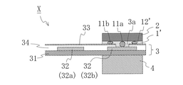
- FIG. 2 shows an example in which the conductive adhesive is applied to a printed wiring board with a reinforcing member.
- the printed wiring board X with a reinforcing member which is an embodiment of the printed wiring board with a reinforcing member, includes a printed wiring board 3 and a conductive adhesive 1'provided on the printed wiring board 3.
- a conductive reinforcing member 2 provided on the conductive adhesive 1'.
- the printed wiring board 3 covers and protects the base member 31, the circuit pattern 32 partially provided on the surface of the base member 31, the insulation protection layer 33 that covers and protects the circuit pattern 32, and the circuit pattern 32. It has an adhesive 34 for adhering the 32 and the base member 31 and the insulating protective layer 33.
- the circuit pattern 32 includes a plurality of signal circuits 32a and a ground circuit 32b.
- the adhesive 34 and the insulating protective layer 33 on the ground circuit 32b are formed with an opening (through hole) 3a that penetrates the adhesive 34 and the insulating protective layer 33 in the thickness direction.
- the conductive adhesive 1' is adhered to the surface of the insulating protective layer 33 of the printed wiring board 3 so as to cover and close the opening 3a, and the binder component (adhesive component) 12'fills the opening 3a. ..
- the conductive adhesive 1' is formed of metal particles (A) 11a and 11b and a binder component (adhesive component) 12'.
- the conductive adhesive 1' has a thick film portion having a relatively thick adhesive and a thin film portion having a relatively thin adhesive. The thick film portion corresponds to the portion filling the opening 3a, and the thin film portion corresponds to the portion located between the insulating protective layer 33 and the reinforcing member 2.
- the metal particles (A) 11a in the thick film portion are located between the reinforcing member 2 and the ground circuit 32b, and preferably contact and conduct the reinforcing member 2 and the ground circuit 32b.
- the thickness of the adhesive in the thick film portion is, for example, 50% or more (preferably 70% or more, more preferably 90%) with respect to the maximum particle diameter of the metal particles (A) 11a in the thick film portion in the adhesive thickness direction. Above).
- the metal particles (A) 11b in the thin film portion are located between the reinforcing member 2 and the insulating protective layer 33, are compressed and deformed by pressure, and are preferably in contact with the reinforcing member 2 and the insulating protective layer 33.
- the thickness of the adhesive in the thin film portion is, for example, 50% or more (preferably 70% or more, more preferably 90% or more) with respect to the maximum particle diameter of the metal particles (A) 11b in the thin film portion in the adhesive thickness direction. Is.
- the gland member 32b and the reinforcing member 2 are electrically connected to each other via the metal particles (A) 11a, the reinforcing member 2 functions as an external connecting conductive layer, and the surface of the reinforcing member 2 is externally grounded. It is electrically connected to the member.
- the metal particles (A) 11 are compressionally deformed, so that they are unlikely to rise on the back side of the base member 31 on which the ground circuit 32b is formed. As a result, when the electronic component 4 is mounted, the adhesion between the printed wiring board 3 and the electronic component 4 is less likely to be hindered. Further, when the metal particles (A) 11a contain a low melting point metal, it is presumed that an alloy is formed at the interface between the gland circuit 32b and the reinforcing member 2 at the time of thermocompression bonding, and the connection stability is better. It becomes.
- the conductive adhesive 1' is, for example, a printed wiring board after the conductive adhesive 1 before flow or before curing, which forms the conductive adhesive 1', is bonded to the surface of the reinforcing member 2 as needed.
- the metal particles (A) 11 are sandwiched between the reinforcing member 2 and the insulating protective layer 33 by adhering them on the insulating protective layer 33 in No. 3 and then flowing or curing the binder component 12 by heating and thermocompression bonding.
- the binder component 12 is allowed to flow to fill the opening 3a while adhering the binder component (adhesive component) 12 to the insulating protective layer 33 while compressing and deforming the metal particles (A) 11b. It can be obtained by curing to form a binder component 12'.
- Both the conductive adhesive 1'and the pre-flow or pre-cured conductive adhesive 1 that forms the conductive adhesive 1' corresponds to the conductive adhesive of the present disclosure.
- the electronic component 4 is connected to the mounting portion provided on the opposite surface of the printed wiring board 3 with respect to the reinforcing member 2.
- the reinforcing member 2 is arranged to face the mounting portion to which the electronic component 4 is connected. As a result, the reinforcing member 2 reinforces the mounting portion of the electronic component 4.
- the conductive reinforcing member 2 is electrically connected to the ground circuit 32b in the printed wiring board 3 via the conductive adhesive 1'. As a result, the reinforcing member 2 is maintained at the same potential as the ground circuit 32, so that noise such as electromagnetic waves from the outside is shielded from the mounting portion of the electronic component 4.
- the conductive adhesive 1' has excellent connection stability between adherends which are conductive members (that is, the reinforcing member 2 and the ground circuit 32b), and the connection stability is maintained even when exposed to a high temperature. Moreover, it is unlikely to cause a ridge on the back side (that is, the surface on which the electronic component 4 is mounted) of the ground circuit 32b and the base member 31, which are adherends. Therefore, when thermocompression bonding is performed to form the conductive adhesive 1', even if the metal particles (A) 11 are pushed in, they are unlikely to rise on the back side of the base member 31 on which the ground circuit 32b is formed. As a result, when the electronic component 4 is mounted, the adhesion between the printed wiring board 3 and the electronic component 4 is less likely to be hindered.
- Example 1 65 parts by mass of bisphenol A type epoxy resin (trade name “jER1256”, manufactured by Mitsubishi Chemical Co., Ltd.) and curing agent (trade name “ST14", Mitsubishi Chemical Co., Ltd.) in toluene so that the solid content is 20% by mass.
- the adhesive composition was prepared by blending 0.05 parts by mass and 35 parts by mass of metal particles with stirring. The properties of the metal particles are as shown in Table 1.
- the obtained adhesive composition was applied to the mold release-treated surface of the PET film whose surface was mold-released, and the solvent was removed by heating to form an anisotropic conductive adhesive.
- Examples 2 to 8 and Comparative Examples 1 to 3 An anisotropic conductive adhesive was prepared in the same manner as in Example 1 except that the types of metal particles in the conductive adhesive and the thickness of the conductive adhesive were changed as shown in Table 1. The properties of the metal particles used in each example are as shown in Table 1, and the ratio in the composition indicates the mass ratio.
- Example 9 35.75 parts by mass of bisphenol A type epoxy resin (trade name “jER1256”, manufactured by Mitsubishi Chemical Co., Ltd.), curing agent (trade name “ST14”, Mitsubishi Chemical) in toluene so that the solid content is 20% by mass. (Manufactured by Co., Ltd.) was blended in an amount of 0.05 parts by mass, silver-coated copper powder (median diameter: 5 ⁇ m) by 29.25 parts by mass, and metal particles by 35 parts by mass, and the mixture was stirred and mixed to prepare an adhesive composition. The properties of the metal particles are as shown in Table 2. The obtained adhesive composition was applied to the mold release-treated surface of the PET film whose surface was mold-released, and the solvent was removed by heating to form an isotropic conductive adhesive.
- Examples 10 to 15 and Comparative Example 4 Isotropic conductivity is the same as in Example 9 except that the types of metal particles (metal particles other than silver-coated copper powder) and the thickness of the conductive adhesive in the conductive adhesive are changed as shown in Table 2. An adhesive was made. The properties of the metal particles used in each example are as shown in Table 2, and the ratio in the composition indicates the mass ratio.
- the median diameter of the metal particles was measured using a flow-type particle image analyzer (trade name “FPIA-3000”, manufactured by Sysmex Corporation). Specifically, the measurement was performed with a metal particle dispersion adjusted to a concentration of 4000 to 20000 pieces / ⁇ l in the LPF measurement mode in a bright field optical system using a 10x objective lens.
- the above metal particle dispersion is prepared by adding 0.1 to 0.5 ml of a surfactant to an aqueous solution of sodium hexametaphosphate adjusted to 0.2% by mass and adding 0.1 ⁇ 0.01 g of metal particles as a measurement sample. did.
- the suspension in which the metal particles were dispersed was subjected to a dispersion treatment for 1 to 3 minutes with an ultrasonic disperser and used for measurement.
- the median diameters of the metal particles obtained by the measurement are shown in Tables 1 and 2.
- the 20% compressive strength under 170 ° C environment was measured according to JIS Z 8844: 2019. Specifically, using a microcompression tester (model "MCT-510", manufactured by Shimadzu Corporation), the tip terminal is ⁇ 50 ⁇ m, and the test speed is 4 mN / sec to 15 mN / sec (particles) in an environment of 170 ° C. (Change as appropriate depending on the hardness of).
- the printed wiring board has two copper foil patterns (thickness: 18 ⁇ m, line width: 3 mm) extending in parallel at intervals on a base member made of a polyimide film having a thickness of 12.5 ⁇ m.
- the insulating protective layer has an insulating protective layer (thickness: 25 ⁇ m) made of an insulating adhesive (thickness: 13 ⁇ m) and a polyimide having a thickness of 25 ⁇ m.
- a cylindrical opening (diameter: 1 mm) that exposes each copper foil pattern is provided. When the conductive adhesive and the printed wiring board were overlapped, this opening was completely covered with the conductive adhesive. Then, the electric resistance value between the obtained copper foil pattern of the evaluation board and the SUS plate is measured using a resistance meter, and the resistance value (initial resistance value) between the printed wiring board and the SUS plate before reflow is used. did.
- Circularity 4 ⁇ ⁇ (area) / (perimeter) 2
- the conductive adhesive of the embodiment has a small initial resistance value, excellent connection stability between adherends which are conductive members, a large circularity, and is unlikely to cause bulging to the back side of the adherend. rice field.
- the resistance value and the rate of change in resistance value after reflow were small, and it was evaluated that good conductivity was maintained even when exposed to high temperatures.
- the 20% compressive strength was high in an environment of 170 ° C. (Comparative Examples 1 to 4)
- a ridge was generated on the back side of the adherend, and the circularity could not be measured.
- Comparative Examples 1 and 2 the shape of the circle to be measured for the circularity is deformed due to the bulge on the back side of the adherend, and the measurement is impossible.
- Comparative Examples 3 and 4 the cover is covered. Due to the large number of ridges on the back side of the body, it was not possible to recognize the circle to be measured for the circularity, and it was impossible to measure. Further, as compared with Example 1 and Example 2, when the content ratio of tin in the metal particles (A) was high, the rate of change in resistance value was lower.
Landscapes
- Chemical & Material Sciences (AREA)
- Organic Chemistry (AREA)
- Engineering & Computer Science (AREA)
- Microelectronics & Electronic Packaging (AREA)
- Manufacturing & Machinery (AREA)
- Inorganic Chemistry (AREA)
- Adhesives Or Adhesive Processes (AREA)
- Conductive Materials (AREA)
- Health & Medical Sciences (AREA)
- Chemical Kinetics & Catalysis (AREA)
- Medicinal Chemistry (AREA)
- Polymers & Plastics (AREA)
- Electric Connection Of Electric Components To Printed Circuits (AREA)
Priority Applications (4)
| Application Number | Priority Date | Filing Date | Title |
|---|---|---|---|
| CN202180007266.7A CN114830843B (zh) | 2020-07-31 | 2021-07-14 | 导电性胶粘剂 |
| US17/783,918 US11597858B1 (en) | 2020-07-31 | 2021-07-14 | Conductive adhesive |
| JP2022506844A JP7037004B1 (ja) | 2020-07-31 | 2021-07-14 | 導電性接着剤 |
| KR1020237001080A KR102823854B1 (ko) | 2020-07-31 | 2021-07-14 | 도전성 접착제 |
Applications Claiming Priority (2)
| Application Number | Priority Date | Filing Date | Title |
|---|---|---|---|
| JP2020130313 | 2020-07-31 | ||
| JP2020-130313 | 2020-07-31 |
Publications (1)
| Publication Number | Publication Date |
|---|---|
| WO2022024757A1 true WO2022024757A1 (ja) | 2022-02-03 |
Family
ID=80036314
Family Applications (1)
| Application Number | Title | Priority Date | Filing Date |
|---|---|---|---|
| PCT/JP2021/026413 Ceased WO2022024757A1 (ja) | 2020-07-31 | 2021-07-14 | 導電性接着剤 |
Country Status (6)
| Country | Link |
|---|---|
| US (1) | US11597858B1 (https=) |
| JP (1) | JP7037004B1 (https=) |
| KR (1) | KR102823854B1 (https=) |
| CN (1) | CN114830843B (https=) |
| TW (1) | TWI859458B (https=) |
| WO (1) | WO2022024757A1 (https=) |
Cited By (2)
| Publication number | Priority date | Publication date | Assignee | Title |
|---|---|---|---|---|
| WO2023182329A1 (ja) * | 2022-03-24 | 2023-09-28 | タツタ電線株式会社 | 熱伝導性導電層 |
| WO2024071400A1 (ja) * | 2022-09-30 | 2024-04-04 | タツタ電線株式会社 | 導電性接着剤層 |
Citations (2)
| Publication number | Priority date | Publication date | Assignee | Title |
|---|---|---|---|---|
| JP2006298954A (ja) * | 2005-04-15 | 2006-11-02 | Tatsuta System Electronics Kk | 導電性接着シート及び回路基板 |
| JP2009218443A (ja) * | 2008-03-11 | 2009-09-24 | Sumitomo Electric Ind Ltd | 金属補強板を備えたフレキシブルプリント配線板 |
Family Cites Families (8)
| Publication number | Priority date | Publication date | Assignee | Title |
|---|---|---|---|---|
| JP3561748B2 (ja) * | 1994-10-14 | 2004-09-02 | 綜研化学株式会社 | 異方導電性接着剤 |
| JP4107769B2 (ja) * | 1999-07-15 | 2008-06-25 | 信越ポリマー株式会社 | 異方導電性接着剤用導電性付与粒子及びこれを用いた異方導電性接着剤 |
| JP5395854B2 (ja) | 2011-08-11 | 2014-01-22 | タツタ電線株式会社 | プリント配線板及びプリント配線板の製造方法 |
| TWI704196B (zh) * | 2016-03-29 | 2020-09-11 | 日商拓自達電線股份有限公司 | 導電性塗料及使用其之屏蔽封裝體之製造方法 |
| TWI770013B (zh) * | 2016-03-29 | 2022-07-11 | 日商拓自達電線股份有限公司 | 導電性塗料及使用其之屏蔽封裝體之製造方法 |
| JP7069162B2 (ja) * | 2017-07-11 | 2022-05-17 | 田中貴金属工業株式会社 | 導電性接着剤組成物 |
| WO2020004510A1 (ja) * | 2018-06-26 | 2020-01-02 | 日立化成株式会社 | 異方性導電フィルム及びその製造方法並びに接続構造体の製造方法 |
| TWI796476B (zh) * | 2018-10-22 | 2023-03-21 | 日商拓自達電線股份有限公司 | 導電性接著片 |
-
2021
- 2021-07-14 WO PCT/JP2021/026413 patent/WO2022024757A1/ja not_active Ceased
- 2021-07-14 CN CN202180007266.7A patent/CN114830843B/zh active Active
- 2021-07-14 US US17/783,918 patent/US11597858B1/en active Active
- 2021-07-14 JP JP2022506844A patent/JP7037004B1/ja active Active
- 2021-07-14 KR KR1020237001080A patent/KR102823854B1/ko active Active
- 2021-07-20 TW TW110126625A patent/TWI859458B/zh active
Patent Citations (2)
| Publication number | Priority date | Publication date | Assignee | Title |
|---|---|---|---|---|
| JP2006298954A (ja) * | 2005-04-15 | 2006-11-02 | Tatsuta System Electronics Kk | 導電性接着シート及び回路基板 |
| JP2009218443A (ja) * | 2008-03-11 | 2009-09-24 | Sumitomo Electric Ind Ltd | 金属補強板を備えたフレキシブルプリント配線板 |
Cited By (5)
| Publication number | Priority date | Publication date | Assignee | Title |
|---|---|---|---|---|
| WO2023182329A1 (ja) * | 2022-03-24 | 2023-09-28 | タツタ電線株式会社 | 熱伝導性導電層 |
| WO2024071400A1 (ja) * | 2022-09-30 | 2024-04-04 | タツタ電線株式会社 | 導電性接着剤層 |
| JP7494411B1 (ja) * | 2022-09-30 | 2024-06-03 | タツタ電線株式会社 | 導電性接着剤層 |
| JP7496949B1 (ja) | 2022-09-30 | 2024-06-07 | タツタ電線株式会社 | 導電性接着剤層 |
| JP2024094389A (ja) * | 2022-09-30 | 2024-07-09 | タツタ電線株式会社 | 導電性接着剤層 |
Also Published As
| Publication number | Publication date |
|---|---|
| TWI859458B (zh) | 2024-10-21 |
| US11597858B1 (en) | 2023-03-07 |
| JPWO2022024757A1 (https=) | 2022-02-03 |
| KR102823854B1 (ko) | 2025-06-20 |
| US20230048469A1 (en) | 2023-02-16 |
| CN114830843B (zh) | 2024-06-18 |
| KR20230043820A (ko) | 2023-03-31 |
| TW202208575A (zh) | 2022-03-01 |
| CN114830843A (zh) | 2022-07-29 |
| JP7037004B1 (ja) | 2022-03-15 |
Similar Documents
| Publication | Publication Date | Title |
|---|---|---|
| JP6597927B1 (ja) | 電磁波シールドシート、および電磁波シールド性配線回路基板 | |
| JP2018039959A (ja) | 導電性接着剤組成物 | |
| CN105684559B (zh) | 印刷配线板、印刷配线板的制造方法及电子装置 | |
| TWI734574B (zh) | 電磁波屏蔽片及電磁波屏蔽性配線電路基板 | |
| JP7037004B1 (ja) | 導電性接着剤 | |
| JP6794591B1 (ja) | 導電性接着シート | |
| JP6650660B2 (ja) | フレキシブルプリント配線板用電磁波シールドシート、および電磁波シールドシート付きフレキシブルプリント配線板 | |
| JP7289993B2 (ja) | 導電性接着剤層 | |
| JP7506150B2 (ja) | 電磁波シールドフィルム | |
| JP7496949B1 (ja) | 導電性接着剤層 | |
| KR102094305B1 (ko) | 회로 접속 재료 | |
| US20250197694A1 (en) | Thermally-conductive electrical conducting layer | |
| JP6991400B1 (ja) | グランド接続引き出しフィルム | |
| WO2025205404A1 (ja) | 熱伝導性導電接着剤層 | |
| JP7654579B2 (ja) | 電磁波シールドフィルム、及び電磁波シールドフィルム付きプリント配線板 | |
| HK40114151A (zh) | 导电性粘接剂层和散热结构 | |
| JP2021027313A (ja) | 電磁波シールドシート、および電磁波シールド性配線回路基板 |
Legal Events
| Date | Code | Title | Description |
|---|---|---|---|
| ENP | Entry into the national phase |
Ref document number: 2022506844 Country of ref document: JP Kind code of ref document: A |
|
| 121 | Ep: the epo has been informed by wipo that ep was designated in this application |
Ref document number: 21850251 Country of ref document: EP Kind code of ref document: A1 |
|
| NENP | Non-entry into the national phase |
Ref country code: DE |
|
| 122 | Ep: pct application non-entry in european phase |
Ref document number: 21850251 Country of ref document: EP Kind code of ref document: A1 |