WO2024071400A1 - 導電性接着剤層 - Google Patents
導電性接着剤層 Download PDFInfo
- Publication number
- WO2024071400A1 WO2024071400A1 PCT/JP2023/035699 JP2023035699W WO2024071400A1 WO 2024071400 A1 WO2024071400 A1 WO 2024071400A1 JP 2023035699 W JP2023035699 W JP 2023035699W WO 2024071400 A1 WO2024071400 A1 WO 2024071400A1
- Authority
- WO
- WIPO (PCT)
- Prior art keywords
- metal particles
- adhesive layer
- conductive adhesive
- particles
- mass
- Prior art date
Links
- 239000012790 adhesive layer Substances 0.000 title claims abstract description 131
- 239000002923 metal particle Substances 0.000 claims abstract description 161
- 239000002245 particle Substances 0.000 claims abstract description 72
- 229910000679 solder Inorganic materials 0.000 claims abstract description 43
- 239000011230 binding agent Substances 0.000 claims abstract description 38
- 238000002844 melting Methods 0.000 claims abstract description 18
- 230000008018 melting Effects 0.000 claims abstract description 18
- 230000006835 compression Effects 0.000 abstract description 7
- 238000007906 compression Methods 0.000 abstract description 7
- 230000001747 exhibiting effect Effects 0.000 abstract description 3
- 239000000853 adhesive Substances 0.000 description 32
- 230000001070 adhesive effect Effects 0.000 description 32
- 230000003014 reinforcing effect Effects 0.000 description 27
- 229920005989 resin Polymers 0.000 description 26
- 239000011347 resin Substances 0.000 description 26
- 229910052751 metal Inorganic materials 0.000 description 23
- 239000002184 metal Substances 0.000 description 23
- 239000003822 epoxy resin Substances 0.000 description 22
- 229920000647 polyepoxide Polymers 0.000 description 22
- LNEPOXFFQSENCJ-UHFFFAOYSA-N haloperidol Chemical compound C1CC(O)(C=2C=CC(Cl)=CC=2)CCN1CCCC(=O)C1=CC=C(F)C=C1 LNEPOXFFQSENCJ-UHFFFAOYSA-N 0.000 description 21
- 239000010408 film Substances 0.000 description 14
- 229920001187 thermosetting polymer Polymers 0.000 description 14
- RYGMFSIKBFXOCR-UHFFFAOYSA-N Copper Chemical compound [Cu] RYGMFSIKBFXOCR-UHFFFAOYSA-N 0.000 description 12
- 239000010949 copper Substances 0.000 description 11
- 239000010931 gold Substances 0.000 description 11
- PXHVJJICTQNCMI-UHFFFAOYSA-N Nickel Chemical compound [Ni] PXHVJJICTQNCMI-UHFFFAOYSA-N 0.000 description 10
- ATJFFYVFTNAWJD-UHFFFAOYSA-N Tin Chemical compound [Sn] ATJFFYVFTNAWJD-UHFFFAOYSA-N 0.000 description 10
- 229910052802 copper Inorganic materials 0.000 description 10
- 238000012545 processing Methods 0.000 description 10
- 239000011241 protective layer Substances 0.000 description 10
- BQCADISMDOOEFD-UHFFFAOYSA-N Silver Chemical compound [Ag] BQCADISMDOOEFD-UHFFFAOYSA-N 0.000 description 9
- 150000001875 compounds Chemical class 0.000 description 9
- 229910052709 silver Inorganic materials 0.000 description 9
- 239000004332 silver Substances 0.000 description 9
- 239000010410 layer Substances 0.000 description 8
- 150000002739 metals Chemical class 0.000 description 7
- 239000000203 mixture Substances 0.000 description 7
- YXFVVABEGXRONW-UHFFFAOYSA-N Toluene Chemical compound CC1=CC=CC=C1 YXFVVABEGXRONW-UHFFFAOYSA-N 0.000 description 6
- IISBACLAFKSPIT-UHFFFAOYSA-N bisphenol A Chemical compound C=1C=C(O)C=CC=1C(C)(C)C1=CC=C(O)C=C1 IISBACLAFKSPIT-UHFFFAOYSA-N 0.000 description 6
- 238000005259 measurement Methods 0.000 description 6
- 229920003986 novolac Polymers 0.000 description 6
- 238000007747 plating Methods 0.000 description 6
- 229910045601 alloy Inorganic materials 0.000 description 5
- 239000000956 alloy Substances 0.000 description 5
- 229910052797 bismuth Inorganic materials 0.000 description 5
- JCXGWMGPZLAOME-UHFFFAOYSA-N bismuth atom Chemical compound [Bi] JCXGWMGPZLAOME-UHFFFAOYSA-N 0.000 description 5
- 239000003795 chemical substances by application Substances 0.000 description 5
- 230000000052 comparative effect Effects 0.000 description 5
- 229910052759 nickel Inorganic materials 0.000 description 5
- 239000000758 substrate Substances 0.000 description 5
- KDLHZDBZIXYQEI-UHFFFAOYSA-N Palladium Chemical compound [Pd] KDLHZDBZIXYQEI-UHFFFAOYSA-N 0.000 description 4
- BASFCYQUMIYNBI-UHFFFAOYSA-N platinum Chemical compound [Pt] BASFCYQUMIYNBI-UHFFFAOYSA-N 0.000 description 4
- ZWEHNKRNPOVVGH-UHFFFAOYSA-N 2-Butanone Chemical compound CCC(C)=O ZWEHNKRNPOVVGH-UHFFFAOYSA-N 0.000 description 3
- CSCPPACGZOOCGX-UHFFFAOYSA-N Acetone Chemical compound CC(C)=O CSCPPACGZOOCGX-UHFFFAOYSA-N 0.000 description 3
- OKTJSMMVPCPJKN-UHFFFAOYSA-N Carbon Chemical compound [C] OKTJSMMVPCPJKN-UHFFFAOYSA-N 0.000 description 3
- LFQSCWFLJHTTHZ-UHFFFAOYSA-N Ethanol Chemical compound CCO LFQSCWFLJHTTHZ-UHFFFAOYSA-N 0.000 description 3
- OKKJLVBELUTLKV-UHFFFAOYSA-N Methanol Chemical compound OC OKKJLVBELUTLKV-UHFFFAOYSA-N 0.000 description 3
- ZMXDDKWLCZADIW-UHFFFAOYSA-N N,N-Dimethylformamide Chemical compound CN(C)C=O ZMXDDKWLCZADIW-UHFFFAOYSA-N 0.000 description 3
- 239000006185 dispersion Substances 0.000 description 3
- 229910002804 graphite Inorganic materials 0.000 description 3
- 239000010439 graphite Substances 0.000 description 3
- -1 polypropylene Polymers 0.000 description 3
- 239000002904 solvent Substances 0.000 description 3
- 238000012360 testing method Methods 0.000 description 3
- 229920005992 thermoplastic resin Polymers 0.000 description 3
- KJCVRFUGPWSIIH-UHFFFAOYSA-N 1-naphthol Chemical compound C1=CC=C2C(O)=CC=CC2=C1 KJCVRFUGPWSIIH-UHFFFAOYSA-N 0.000 description 2
- 229930185605 Bisphenol Natural products 0.000 description 2
- 229920002799 BoPET Polymers 0.000 description 2
- UFWIBTONFRDIAS-UHFFFAOYSA-N Naphthalene Chemical compound C1=CC=CC2=CC=CC=C21 UFWIBTONFRDIAS-UHFFFAOYSA-N 0.000 description 2
- ISWSIDIOOBJBQZ-UHFFFAOYSA-N Phenol Chemical compound OC1=CC=CC=C1 ISWSIDIOOBJBQZ-UHFFFAOYSA-N 0.000 description 2
- 238000004220 aggregation Methods 0.000 description 2
- 230000002776 aggregation Effects 0.000 description 2
- PXKLMJQFEQBVLD-UHFFFAOYSA-N bisphenol F Chemical compound C1=CC(O)=CC=C1CC1=CC=C(O)C=C1 PXKLMJQFEQBVLD-UHFFFAOYSA-N 0.000 description 2
- 239000000470 constituent Substances 0.000 description 2
- 239000011889 copper foil Substances 0.000 description 2
- GYZLOYUZLJXAJU-UHFFFAOYSA-N diglycidyl ether Chemical compound C1OC1COCC1CO1 GYZLOYUZLJXAJU-UHFFFAOYSA-N 0.000 description 2
- ZUOUZKKEUPVFJK-UHFFFAOYSA-N diphenyl Chemical compound C1=CC=CC=C1C1=CC=CC=C1 ZUOUZKKEUPVFJK-UHFFFAOYSA-N 0.000 description 2
- 238000011156 evaluation Methods 0.000 description 2
- PCHJSUWPFVWCPO-UHFFFAOYSA-N gold Chemical compound [Au] PCHJSUWPFVWCPO-UHFFFAOYSA-N 0.000 description 2
- 229910052737 gold Inorganic materials 0.000 description 2
- 238000010438 heat treatment Methods 0.000 description 2
- 238000010030 laminating Methods 0.000 description 2
- 239000000155 melt Substances 0.000 description 2
- 238000000034 method Methods 0.000 description 2
- 238000002156 mixing Methods 0.000 description 2
- AFEQENGXSMURHA-UHFFFAOYSA-N oxiran-2-ylmethanamine Chemical compound NCC1CO1 AFEQENGXSMURHA-UHFFFAOYSA-N 0.000 description 2
- 229910052763 palladium Inorganic materials 0.000 description 2
- 229910052697 platinum Inorganic materials 0.000 description 2
- 229920001721 polyimide Polymers 0.000 description 2
- 239000007787 solid Substances 0.000 description 2
- 239000010409 thin film Substances 0.000 description 2
- STHCTMWQPJVCGN-UHFFFAOYSA-N 2-[[2-[1,1,2-tris[2-(oxiran-2-ylmethoxy)phenyl]ethyl]phenoxy]methyl]oxirane Chemical compound C1OC1COC1=CC=CC=C1CC(C=1C(=CC=CC=1)OCC1OC1)(C=1C(=CC=CC=1)OCC1OC1)C1=CC=CC=C1OCC1CO1 STHCTMWQPJVCGN-UHFFFAOYSA-N 0.000 description 1
- UJWXADOOYOEBCW-UHFFFAOYSA-N 2-[[2-[bis[2-(oxiran-2-ylmethoxy)phenyl]methyl]phenoxy]methyl]oxirane Chemical compound C1OC1COC1=CC=CC=C1C(C=1C(=CC=CC=1)OCC1OC1)C1=CC=CC=C1OCC1CO1 UJWXADOOYOEBCW-UHFFFAOYSA-N 0.000 description 1
- QTWJRLJHJPIABL-UHFFFAOYSA-N 2-methylphenol;3-methylphenol;4-methylphenol Chemical compound CC1=CC=C(O)C=C1.CC1=CC=CC(O)=C1.CC1=CC=CC=C1O QTWJRLJHJPIABL-UHFFFAOYSA-N 0.000 description 1
- VEORPZCZECFIRK-UHFFFAOYSA-N 3,3',5,5'-tetrabromobisphenol A Chemical compound C=1C(Br)=C(O)C(Br)=CC=1C(C)(C)C1=CC(Br)=C(O)C(Br)=C1 VEORPZCZECFIRK-UHFFFAOYSA-N 0.000 description 1
- VPWNQTHUCYMVMZ-UHFFFAOYSA-N 4,4'-sulfonyldiphenol Chemical compound C1=CC(O)=CC=C1S(=O)(=O)C1=CC=C(O)C=C1 VPWNQTHUCYMVMZ-UHFFFAOYSA-N 0.000 description 1
- 229920000178 Acrylic resin Polymers 0.000 description 1
- 239000004925 Acrylic resin Substances 0.000 description 1
- 238000012935 Averaging Methods 0.000 description 1
- 229910000881 Cu alloy Inorganic materials 0.000 description 1
- 239000004593 Epoxy Substances 0.000 description 1
- JOYRKODLDBILNP-UHFFFAOYSA-N Ethyl urethane Chemical compound CCOC(N)=O JOYRKODLDBILNP-UHFFFAOYSA-N 0.000 description 1
- 229920000877 Melamine resin Polymers 0.000 description 1
- 239000004642 Polyimide Substances 0.000 description 1
- 239000004743 Polypropylene Substances 0.000 description 1
- 229910020830 Sn-Bi Inorganic materials 0.000 description 1
- 229910018728 Sn—Bi Inorganic materials 0.000 description 1
- XTXRWKRVRITETP-UHFFFAOYSA-N Vinyl acetate Chemical compound CC(=O)OC=C XTXRWKRVRITETP-UHFFFAOYSA-N 0.000 description 1
- HCHKCACWOHOZIP-UHFFFAOYSA-N Zinc Chemical compound [Zn] HCHKCACWOHOZIP-UHFFFAOYSA-N 0.000 description 1
- 239000006096 absorbing agent Substances 0.000 description 1
- 125000003647 acryloyl group Chemical group O=C([*])C([H])=C([H])[H] 0.000 description 1
- 229920000180 alkyd Polymers 0.000 description 1
- 229910002065 alloy metal Inorganic materials 0.000 description 1
- 238000005275 alloying Methods 0.000 description 1
- 229910052787 antimony Inorganic materials 0.000 description 1
- WATWJIUSRGPENY-UHFFFAOYSA-N antimony atom Chemical compound [Sb] WATWJIUSRGPENY-UHFFFAOYSA-N 0.000 description 1
- 239000003963 antioxidant agent Substances 0.000 description 1
- 239000007864 aqueous solution Substances 0.000 description 1
- 239000004305 biphenyl Substances 0.000 description 1
- 235000010290 biphenyl Nutrition 0.000 description 1
- 239000002981 blocking agent Substances 0.000 description 1
- QHIWVLPBUQWDMQ-UHFFFAOYSA-N butyl prop-2-enoate;methyl 2-methylprop-2-enoate;prop-2-enoic acid Chemical compound OC(=O)C=C.COC(=O)C(C)=C.CCCCOC(=O)C=C QHIWVLPBUQWDMQ-UHFFFAOYSA-N 0.000 description 1
- 238000006243 chemical reaction Methods 0.000 description 1
- 238000000576 coating method Methods 0.000 description 1
- 239000003086 colorant Substances 0.000 description 1
- 239000007822 coupling agent Substances 0.000 description 1
- 229930003836 cresol Natural products 0.000 description 1
- 239000003085 diluting agent Substances 0.000 description 1
- 230000000694 effects Effects 0.000 description 1
- 230000005611 electricity Effects 0.000 description 1
- 239000000835 fiber Substances 0.000 description 1
- 239000000945 filler Substances 0.000 description 1
- 239000003063 flame retardant Substances 0.000 description 1
- 230000006872 improvement Effects 0.000 description 1
- 229910052738 indium Inorganic materials 0.000 description 1
- APFVFJFRJDLVQX-UHFFFAOYSA-N indium atom Chemical compound [In] APFVFJFRJDLVQX-UHFFFAOYSA-N 0.000 description 1
- 239000011133 lead Substances 0.000 description 1
- 238000004519 manufacturing process Methods 0.000 description 1
- JDSHMPZPIAZGSV-UHFFFAOYSA-N melamine Chemical compound NC1=NC(N)=NC(N)=N1 JDSHMPZPIAZGSV-UHFFFAOYSA-N 0.000 description 1
- 230000003287 optical effect Effects 0.000 description 1
- 239000003960 organic solvent Substances 0.000 description 1
- 150000002989 phenols Chemical class 0.000 description 1
- IGALFTFNPPBUDN-UHFFFAOYSA-N phenyl-[2,3,4,5-tetrakis(oxiran-2-ylmethyl)phenyl]methanediamine Chemical compound C=1C(CC2OC2)=C(CC2OC2)C(CC2OC2)=C(CC2OC2)C=1C(N)(N)C1=CC=CC=C1 IGALFTFNPPBUDN-UHFFFAOYSA-N 0.000 description 1
- 239000002985 plastic film Substances 0.000 description 1
- 229920006255 plastic film Polymers 0.000 description 1
- 239000004014 plasticizer Substances 0.000 description 1
- 229920001225 polyester resin Polymers 0.000 description 1
- 239000004645 polyester resin Substances 0.000 description 1
- 229920013716 polyethylene resin Polymers 0.000 description 1
- 239000009719 polyimide resin Substances 0.000 description 1
- 229920005672 polyolefin resin Polymers 0.000 description 1
- 229920001155 polypropylene Polymers 0.000 description 1
- 229920005990 polystyrene resin Polymers 0.000 description 1
- 238000003825 pressing Methods 0.000 description 1
- 230000008569 process Effects 0.000 description 1
- BDERNNFJNOPAEC-UHFFFAOYSA-N propan-1-ol Chemical compound CCCO BDERNNFJNOPAEC-UHFFFAOYSA-N 0.000 description 1
- 239000011342 resin composition Substances 0.000 description 1
- GCLGEJMYGQKIIW-UHFFFAOYSA-H sodium hexametaphosphate Chemical compound [Na]OP1(=O)OP(=O)(O[Na])OP(=O)(O[Na])OP(=O)(O[Na])OP(=O)(O[Na])OP(=O)(O[Na])O1 GCLGEJMYGQKIIW-UHFFFAOYSA-H 0.000 description 1
- 235000019982 sodium hexametaphosphate Nutrition 0.000 description 1
- 125000003003 spiro group Chemical group 0.000 description 1
- 239000007921 spray Substances 0.000 description 1
- 238000003756 stirring Methods 0.000 description 1
- 239000000126 substance Substances 0.000 description 1
- 239000004094 surface-active agent Substances 0.000 description 1
- 239000000725 suspension Substances 0.000 description 1
- 150000003505 terpenes Chemical class 0.000 description 1
- 235000007586 terpenes Nutrition 0.000 description 1
- 239000001577 tetrasodium phosphonato phosphate Substances 0.000 description 1
- 239000004034 viscosity adjusting agent Substances 0.000 description 1
- 229910052725 zinc Inorganic materials 0.000 description 1
- 239000011701 zinc Substances 0.000 description 1
Images

Classifications
-
- C—CHEMISTRY; METALLURGY
- C09—DYES; PAINTS; POLISHES; NATURAL RESINS; ADHESIVES; COMPOSITIONS NOT OTHERWISE PROVIDED FOR; APPLICATIONS OF MATERIALS NOT OTHERWISE PROVIDED FOR
- C09J—ADHESIVES; NON-MECHANICAL ASPECTS OF ADHESIVE PROCESSES IN GENERAL; ADHESIVE PROCESSES NOT PROVIDED FOR ELSEWHERE; USE OF MATERIALS AS ADHESIVES
- C09J201/00—Adhesives based on unspecified macromolecular compounds
-
- C—CHEMISTRY; METALLURGY
- C09—DYES; PAINTS; POLISHES; NATURAL RESINS; ADHESIVES; COMPOSITIONS NOT OTHERWISE PROVIDED FOR; APPLICATIONS OF MATERIALS NOT OTHERWISE PROVIDED FOR
- C09J—ADHESIVES; NON-MECHANICAL ASPECTS OF ADHESIVE PROCESSES IN GENERAL; ADHESIVE PROCESSES NOT PROVIDED FOR ELSEWHERE; USE OF MATERIALS AS ADHESIVES
- C09J7/00—Adhesives in the form of films or foils
- C09J7/30—Adhesives in the form of films or foils characterised by the adhesive composition
-
- C—CHEMISTRY; METALLURGY
- C09—DYES; PAINTS; POLISHES; NATURAL RESINS; ADHESIVES; COMPOSITIONS NOT OTHERWISE PROVIDED FOR; APPLICATIONS OF MATERIALS NOT OTHERWISE PROVIDED FOR
- C09J—ADHESIVES; NON-MECHANICAL ASPECTS OF ADHESIVE PROCESSES IN GENERAL; ADHESIVE PROCESSES NOT PROVIDED FOR ELSEWHERE; USE OF MATERIALS AS ADHESIVES
- C09J9/00—Adhesives characterised by their physical nature or the effects produced, e.g. glue sticks
- C09J9/02—Electrically-conducting adhesives
-
- H—ELECTRICITY
- H01—ELECTRIC ELEMENTS
- H01B—CABLES; CONDUCTORS; INSULATORS; SELECTION OF MATERIALS FOR THEIR CONDUCTIVE, INSULATING OR DIELECTRIC PROPERTIES
- H01B1/00—Conductors or conductive bodies characterised by the conductive materials; Selection of materials as conductors
- H01B1/20—Conductive material dispersed in non-conductive organic material
- H01B1/22—Conductive material dispersed in non-conductive organic material the conductive material comprising metals or alloys
Definitions
- the present invention relates to a conductive adhesive layer.
- Conductive adhesive layers have traditionally been used to connect electronic components.
- One such conductive adhesive layer is known to be an alloy of low-melting-point metal particles and high-melting-point metal particles, which can replace high-temperature solder and provide connection stability (Patent Document 1).
- the present invention aims to solve these problems by providing a conductive adhesive layer that has sufficient adhesive strength for a variety of adherends, even under low-temperature, short-time compression processing conditions.
- the present invention was completed based on this knowledge.
- the present invention provides a conductive adhesive layer that contains a binder component and metal particles A having a melting point of 170°C or less, with the metal A protruding from the surface.
- the conductive adhesive layer contains a binder component and metal particles A with a melting point of 170°C or less, and because the metal particles A protrude from the surface of the conductive adhesive layer, it can exhibit high adhesive strength to a variety of adherends even under low temperature and short compression processing conditions.
- the conductive adhesive layer preferably contains, in addition to the metal particles A, metal particles B that can be alloyed with metal particles A. By including metal particles B, the electrical conductivity and adhesive strength of the conductive adhesive layer can be improved.
- the conductive adhesive layer further contains solder particles C in addition to the metal particles A.
- solder particles C electrical conductivity in the thickness direction can be improved.
- the metal particles A are preferably spherical. When the metal particles A are spherical, the metal particles A are more likely to protrude from the surface of the conductive adhesive layer, making it easier to achieve high adhesion strength.
- the metal particles B are preferably dendritic or flaky. When the metal particles B are dendritic or flaky, it becomes easier to achieve high adhesion strength.
- solder particles C are spherical. By making the solder particles C spherical, the electrical conductivity in the thickness direction can be stabilized without variation.
- the median diameter (D50) of the metal particles A is larger than the film thickness of the conductive adhesive layer.
- the median diameter (D50) of the metal particles A is larger than the film thickness of the conductive adhesive layer, it becomes easier to exhibit adhesion strength under low-temperature, short-time compression processing conditions.
- the thickness of the conductive adhesive layer is preferably 1 to 50 ⁇ m.
- the conductive adhesive layer of the present invention can exert sufficient adhesive strength to various adherends even under low temperature and short pressure processing conditions. In particular, it can exert sufficient adhesive strength even when the adherend is a metal plate or Ni-Au plated.
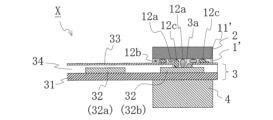
- FIG. 2 is a cross-sectional view showing one embodiment of a conductive adhesive layer of the present invention.
- 1 is a cross-sectional view showing one embodiment of a printed wiring board with a reinforcing member to which a conductive adhesive layer of the present invention is applied.
- the conductive adhesive layer of the present invention includes at least a binder component and metal particles A having a melting point of 170° C. or less, and the metal particles A protrude from the surface of the conductive adhesive layer.
- metal particles A the metal particles having a melting point of 170° C. or less are referred to as "metal particles A”.
- protruding from the surface of the conductive adhesive layer refers to a state in which the conductive particles of the adhesive portion composed of the binder component protrude to a position outside the horizontal plane (specifically, the plane obtained by averaging the height of the surface) of the area where the conductive particles do not protrude before the binder component flows, and for example, an embodiment in which the median diameter (D50) of the metal particles A or the particle thickness described later is larger than the thickness of the conductive adhesive layer.
- the thickness of the conductive adhesive layer refers to the average thickness (for example, the thickness T shown in FIG. 1) in the area where the conductive particles of the adhesive portion composed of the binder component do not protrude before the binder component flows.
- the metal particles A may or may not be covered by the conductive adhesive layer.
- the conductive adhesive layer may be an anisotropic conductive adhesive layer or an isotropic conductive adhesive layer.
- the layer when metal particles A are mainly responsible for the conductivity of the conductive adhesive layer, the layer will be an anisotropic conductive adhesive layer, and when the metal particles A and other conductive particles (for example, metal particles B described below) are mixed in a balanced manner, the layer will be an isotropic conductive adhesive layer.
- the conductive adhesive layer preferably contains metal particles B that can be alloyed with metal particles A and solder particles C.
- metal particles B that can be alloyed with metal particles A and solder particles C in addition to metal particles A, it becomes easier to exert adhesive strength to various adherends even under low temperature and short pressure processing conditions.
- FIG 1 shows one embodiment of the conductive adhesive layer of the present invention.
- the conductive adhesive layer (1) contains a binder component (11), metal particles A (12a), metal particles B (12b) that can be alloyed with the metal particles A, and solder particles C (12c).
- the metal particles A (12a) protrude from the surface of the adhesive layer composed of the binder component (11).
- the metal particles A have a melting point of 170° C. or less, preferably 160° C. or less, and more preferably 150° C. or less.
- the lower limit of the melting point is not particularly limited, but is preferably 130° C. or more.
- the metal particles A are preferably an alloy containing tin (melting point: 232°C) and bismuth (melting point: 271°C), and may contain other metals in addition to tin and bismuth as long as the melting point is within a range of 170°C or less.
- the mass ratio of tin:bismuth in the metal particles A is preferably 30:70 to 80:20, more preferably 35:65 to 60:40, and particularly preferably 40:60 to 45:55.
- the above mass ratio of tin:bismuth makes it easy to adjust the melting point of the metal particles A to within the range of 130°C to 170°C.
- the median diameter (D50) of the metal particles A is preferably larger than the thickness of the conductive adhesive layer, and is preferably 70 to 500% of the thickness of the conductive adhesive layer, more preferably 100 to 400%, and particularly preferably 150 to 300%.
- the maximum particle diameter of the metal particles A is more likely to be larger than the conductive adhesive layer thickness, and as a result, the metal particles A protrude from the surface of the conductive adhesive layer, and the metal particles A melt appropriately when adhering to the adherend, and can exhibit adhesion strength even under low temperature conditions.
- the median diameter (D50) of the metal particles A when the median diameter (D50) of the metal particles A is 100% or more of the conductive adhesive layer thickness, the median diameter (D50) of the metal particles A becomes larger than the thickness of the conductive adhesive layer, and it is easier to protrude from the surface.
- the median diameter (D50) of the metal particles A is 500% or less of the conductive adhesive layer thickness, the adhesion strength to the adherend is better.
- the thickness of the conductive adhesive layer refers to the average thickness of the adhesive portion made of the binder component in the area where no metal particles protrude, before the binder component begins to flow.
- the particle diameter (particle thickness) of the metal particles A in the thickness direction is preferably larger than the thickness of the conductive adhesive layer, and is preferably 100 to 400% of the thickness of the conductive adhesive layer, and more preferably 150 to 300%. By making the particle thickness larger than the thickness of the conductive adhesive layer, the metal particles A are more likely to protrude to the surface.
- the median diameter (D50) of the metal particles A is preferably 3 to 150 ⁇ m, more preferably 5 to 100 ⁇ m, and particularly preferably 10 to 75 ⁇ m. By having the median diameter (D50) of the metal particles A within the above range, it becomes easy to protrude from the surface of the conductive adhesive layer.
- the shape of the metal particles A may be spherical (such as spherical or elliptical), flake-like (scaly or flat), dendritic, fibrous, or amorphous (polyhedral). Of these, from the viewpoint of ease of protruding from the surface of the conductive adhesive layer, spherical shapes are preferred, and spherical shapes are particularly preferred.
- the content of the metal particles A is preferably 50 to 500 parts by mass, more preferably 60 to 400 parts by mass, particularly preferably 70 to 300 parts by mass, and particularly preferably 80 to 200 parts by mass, per 100 parts by mass of the binder component.
- the conductive adhesive layer of the present invention may contain metal particles other than the metal particles A.
- the other metal particles may contain metal particles capable of being alloyed with the metal particles A.
- the metal particles capable of being alloyed with the metal particles A are referred to as "metal particles B capable of being alloyed with the metal particles A" or "metal particles B". Only one type of the metal particles B may be used, or two or more types may be used.
- metal particles B examples include metal particles, metal-coated metal particles, metal-coated resin particles, metal-coated graphite particles, metal-coated alloy particles, resin-coated metal particles, metal fibers, etc.
- the metal particles B may be copper particles, silver-coated copper particles, silver-coated copper alloy particles, nickel particles, silver-coated nickel particles, silver-coated graphite particles, copper-coated graphite particles, resin-coated silver particles, resin-coated copper particles, resin-coated nickel particles, etc.
- metal particles containing copper are preferred, and copper particles and silver-coated copper particles are particularly preferred.
- the shape of the metal particles B may be spherical (such as spherical or elliptical), flake-like (scale-like or flat), dendritic (dendrite-like), fibrous, or amorphous (polyhedral). Among these, flake-like and dendritic shapes are preferred. By making the shape of the metal particles B flake-like or dendritic, the metal particles B tend to overlap each other, which increases the contact between the metal particles B and improves the electrical conductivity in the planar direction.
- the metal particles A melt and alloy, and connect with the metal particles B that can be alloyed with the metal particles A within the conductive adhesive layer, thereby exerting adhesion strength.
- the median diameter (D50) of the metal particles B is preferably smaller than that of the metal particles A, specifically, preferably 0.5 to 25 ⁇ m, more preferably 3 to 10 ⁇ m. If the median diameter (D50) is 0.5 ⁇ m or more, isotropic conductivity is better exhibited. In addition, the dispersibility of the metal particles B is good, and aggregation can be suppressed. If the median diameter (D50) is smaller than that of the metal particles A (particularly if it is 25 ⁇ m or less), the adhesive strength of the conductive adhesive layer to the adherend is superior.
- the content of the metal particles B is preferably less than that of the metal particles A, and is preferably 30 to 300 parts by mass, more preferably 40 to 250 parts by mass, particularly preferably 50 to 200 parts by mass, and particularly preferably 60 to 150 parts by mass, per 100 parts by mass of the binder component. By having the content of the metal particles B within the above range, it becomes easier to exert adhesion strength.
- solder Particle C The conductive adhesive layer of the present invention preferably contains solder particles as the other metal particles. In particular, it is preferable that the conductive adhesive layer further contains solder particles in addition to the metal particles A and B. In this specification, the solder particles are referred to as "solder particles C". As the solder particles C, only one type may be used, or two or more types may be used.
- the solder particles C preferably contain at least tin as a constituent metal.
- the content of tin in the solder particles C is preferably 80% by mass or more, more preferably 85% by mass or more, even more preferably 90% by mass or more, and particularly preferably 94% by mass or more, relative to the total amount of the solder particles C being 100% by mass. It is presumed that the tin in the solder particles C forms an alloy at the interface with the conductive adherend (such as a ground circuit or a reinforcing member on the ground side) during thermocompression bonding.
- the solder particles C contain 80% by mass or more (particularly 90% by mass or more) of tin, the connection stability between the adherends is maintained even when exposed to high temperatures in a reflow process or the like.
- the content is preferably 99.9% by mass or less, more preferably 99.6% by mass or less.
- the solder particles C have a certain degree of hardness, and when high pressure is applied in a high-temperature environment, the solder particles C are not compressed too much, making it easier to ensure electrical continuity between the adherends.
- the solder particles C may contain metals other than tin as constituent metals.
- the other metals include gold, silver, copper, platinum, nickel, zinc, lead, palladium, bismuth, antimony, and indium.
- the solder particles C preferably contain, as the other metals, metals harder than tin, such as gold, silver, copper, platinum, nickel, and palladium.
- the other metals may each contain only one type, or two or more types.
- the shape of the solder particles C may be spherical (e.g., spherical, elliptical, etc.), flake-like (scale-like, flat), dendritic, fibrous, amorphous (polyhedral), etc.
- spherical is preferred, and spherical is particularly preferred.
- the median diameter (D50) of the solder particles C is preferably larger than that of the metal particles B, and is preferably 1 to 150 ⁇ m, more preferably 3 to 150 ⁇ m, even more preferably 5 to 100 ⁇ m, even more preferably 5 to 90 ⁇ m, and particularly preferably 10 to 75 ⁇ m. If the median diameter (D50) is larger than that of the metal particles B (particularly if it is 1 ⁇ m or more), the solder particles C will exhibit better conductivity in the thickness direction. In addition, the metal particles have good dispersibility and aggregation can be suppressed. If the median diameter (D50) is 150 ⁇ m or less (particularly if it is 90 ⁇ m or less), the adhesive strength of the conductive adhesive layer to the adherend will be superior.
- the content of the solder particles C is preferably greater than that of the metal particles B, and is preferably 50 to 500 parts by mass, more preferably 60 to 400 parts by mass, particularly preferably 70 to 300 parts by mass, and particularly preferably 80 to 200 parts by mass, per 100 parts by mass of the binder component.
- the content of the solder particles C is preferably greater than that of the metal particles B (particularly within the above range), it becomes easier to exhibit adhesion strength even under low temperature and short compression processing conditions.
- the conductive adhesive layer may also contain metal particles other than metal particles A, metal particles B, and solder particles C.
- the total amount of metal particles A, metal particles B, and solder particles C is preferably 90 mass% or more, and more preferably 100 mass%, of the total amount of metal particles used in the conductive adhesive layer (100 mass%).
- the total content of metal particles per 100 parts by mass of binder components is preferably 80 to 1000 parts by mass, more preferably 100 to 1000 parts by mass, even more preferably 120 to 700 parts by mass, and particularly preferably 150 to 400 parts by mass.
- the total content of metal particles per 100 parts by mass of binder components is 80 parts by mass or more, it becomes easier to exhibit electrical conductivity, and when the total content of metal particles per 100 parts by mass of binder components is 1000 parts by mass or less, it becomes easier to exhibit sufficient adhesion strength.
- the binder component includes a thermoplastic resin, a thermosetting resin, an active energy ray curable compound, etc.
- the binder component may be used alone or in combination of two or more.
- thermoplastic resin examples include polystyrene resins, vinyl acetate resins, polyester resins, polyolefin resins (e.g., polyethylene resins, polypropylene resin compositions, etc.), polyimide resins, acrylic resins, etc. Only one type of the thermoplastic resins may be used, or two or more types may be used.
- thermosetting resins include both resins having thermosetting properties (thermosetting resins) and resins obtained by curing the above-mentioned thermosetting resins.
- thermosetting resins include phenol-based resins, epoxy-based resins, urethane-based resins, melamine-based resins, and alkyd-based resins. Only one type of the above-mentioned thermosetting resins may be used, or two or more types may be used.
- epoxy resins examples include bisphenol type epoxy resins, spiro ring type epoxy resins, naphthalene type epoxy resins, biphenyl type epoxy resins, terpene type epoxy resins, glycidyl ether type epoxy resins, glycidyl amine type epoxy resins, novolac type epoxy resins, etc.
- the above-mentioned bisphenol type epoxy resins include, for example, bisphenol A type epoxy resins, bisphenol F type epoxy resins, bisphenol S type epoxy resins, and tetrabromobisphenol A type epoxy resins.
- the above-mentioned glycidyl ether type epoxy resins include, for example, tris(glycidyloxyphenyl)methane and tetrakis(glycidyloxyphenyl)ethane.
- the above-mentioned glycidylamine type epoxy resins include, for example, tetraglycidyldiaminodiphenylmethane.
- the above-mentioned novolac type epoxy resins include, for example, cresol novolac type epoxy resins, phenol novolac type epoxy resins, ⁇ -naphthol novolac type epoxy resins, and brominated phenol novolac type epoxy resins.
- the active energy ray curable compound includes both a compound that can be cured by irradiation with active energy rays (active energy ray curable compound) and a compound obtained by curing the active energy ray curable compound.
- the active energy ray curable compound is not particularly limited, but examples thereof include polymerizable compounds having one or more (preferably two or more) radical reactive groups (e.g., (meth)acryloyl groups) in the molecule. Only one type of the active energy ray curable compound may be used, or two or more types may be used.
- thermosetting resins are preferred.
- the binder component after the conductive adhesive layer is placed on an adherend such as a printed wiring board or a shielded printed wiring board that has been treated with electromagnetic shielding measures, the binder component can be cured by applying pressure and heat, resulting in good adhesion at the attachment portion.
- the binder component is a thermosetting resin
- the binder component after thermocompression becomes a thermosetting resin formed by curing the above thermosetting resin.
- the binder component may contain a curing agent for accelerating the thermosetting reaction.
- the curing agent may be appropriately selected depending on the type of the thermosetting resin. Only one type of curing agent may be used, or two or more types may be used.
- the content of the binder component in the conductive adhesive layer is preferably 15 to 95% by mass, more preferably 20 to 90% by mass, and even more preferably 30 to 80% by mass, relative to 100% by mass of the total amount of the conductive adhesive layer. If the content is 15% by mass or more, the adhesion to the adherend is better. If the content is 95% by mass or less, the metal particles A can be sufficiently blended, resulting in better adhesion strength and conductivity.
- the conductive adhesive layer may contain other components in addition to the above-mentioned components, within the range that does not impair the effect of the present invention.
- the other components include components contained in publicly known or commonly used adhesives.
- the other components include curing accelerators, plasticizers, flame retardants, defoamers, viscosity modifiers, antioxidants, diluents, anti-settling agents, fillers, colorants, leveling agents, coupling agents, UV absorbers, tackifier resins, and anti-blocking agents. Only one type of the other components may be used, or two or more types may be used.
- the thickness of the conductive adhesive layer is preferably 3 to 50 ⁇ m, and more preferably 5 to 30 ⁇ m. If the thickness is 3 ⁇ m or more, the adhesive strength to the adherend is better. If the thickness is 50 ⁇ m or less, costs can be reduced and the product including the conductive adhesive layer can be designed to be thin.
- the thickness of the conductive adhesive layer is the thickness in the area where the metal particles A do not protrude. It is also preferable that the thickness of the conductive adhesive layer after press processing is within the above range.
- the adhesive strength (peel force) of the conductive adhesive layer against a metal plate or Ni-Au plating is not particularly limited, but is preferably 7.3 N/cm or more, more preferably 8.0 N/cm or more, even more preferably 9.0 N/cm or more, and particularly preferably 10.0 N/cm or more.
- the Ni-Au plating may be reinforced with a plastic film or the like so that it does not break during the peel test. The specific method of the peel test is as described, for example, in the Examples below.
- the conductive adhesive layer may have a separate film laminated on at least one surface. That is, the conductive adhesive layer may be provided as a laminate including a separate film and the conductive adhesive layer formed on the release surface of the separate film. The separate film is peeled off when in use.
- the conductive adhesive layer can be manufactured by a known or conventional manufacturing method.
- an adhesive composition that forms a conductive adhesive layer can be applied (coated) onto a temporary substrate or substrate such as a separate film, and, if necessary, the adhesive composition is removed and/or partially cured to form the conductive adhesive layer.
- the adhesive composition contains, for example, a solvent in addition to the components contained in the conductive adhesive layer described above.
- the solvent include toluene, acetone, methyl ethyl ketone, methanol, ethanol, propanol, and dimethylformamide.
- the solid content concentration of the adhesive composition is appropriately set according to the thickness of the conductive adhesive layer to be formed, etc.
- a known coating method may be used to apply the adhesive composition.
- a coater such as a gravure roll coater, reverse roll coater, kiss roll coater, lip coater, dip roll coater, bar coater, knife coater, spray coater, comma coater, direct coater, or slot die coater may be used.
- the conductive adhesive layer produced as described above is capable of exerting sufficient adhesive strength under low-temperature, short-time compression processing conditions even when used with a variety of adherends, particularly when the adherend is a metal plate or Ni-Au plated substrate, and is therefore suitable for use in filling holes in printed wiring boards and as a resist ink.
- a printed wiring board with a reinforcing member which is one embodiment of a printed wiring board with a reinforcing member, includes a printed wiring board (3), a conductive adhesive layer (1') provided on the printed wiring board (3), and a reinforcing member (2) having conductivity provided on the conductive adhesive layer (1').
- the printed wiring board (3) has a base member (31), a circuit pattern (32) partially provided on the surface of the base member (31), an insulating protective layer (33) that covers and insulates the circuit pattern (32), and an adhesive (34) that covers the circuit pattern (32) and bonds the circuit pattern (32) and the base member (31) to the insulating protective layer (33).
- the circuit pattern (32) includes a plurality of signal circuits (32a) and ground circuits (32b).
- the adhesive (34) on the ground circuit (32b) and the insulating protective layer (33) have openings (through holes) (3a) that penetrate the adhesive (34) and the insulating protective layer (33) in the thickness direction.
- the conductive adhesive layer (1') is adhered to the surface of the insulating protective layer (33) of the printed wiring board (3) so as to cover and close the opening (3a), and the binder component (11') fills the opening (3a).
- the conductive adhesive layer (1') is formed of metal particles A (12a), metal particles B (12b), solder particles C (12c), and the binder component (11').
- the conductive adhesive layer (1') has a thick film portion where the adhesive layer is relatively thick, and a thin film portion where the adhesive layer is relatively thin. The thick film portion coincides with the portion filling the opening (3a), and the thin film portion coincides with the portion located between the insulating protective layer (33) and the reinforcing member (2).
- the metal particles A (12a) and the solder particles C (12c) in the thick film portion are located between the reinforcing member (2) and the ground circuit (32b), and preferably contact and conduct electricity between the reinforcing member (2) and the ground circuit (32b).
- the metal particles A (12a) protruding from the surface of the conductive adhesive layer (1') adhere to the surface of the ground circuit (32b) and the reinforcing member (2).
- the metal particles B (12b) and solder particles C (12c) are included, so that the ground member (32b) and the reinforcing member (2) are electrically connected, the reinforcing member (2) functions as an external connection conductive layer, and the surface of the reinforcing member (2) is electrically connected to an external ground member.
- the conductive adhesive layer (1') can be obtained, for example, by laminating the conductive adhesive layer (1) before flow or hardening to form the conductive adhesive layer (1') on the surface of the reinforcing member (2) as necessary, then laminating it on the insulating protective layer (33) of the printed wiring board (3), and then heating to flow or harden the binder component (11) and thermocompression bonding, so that a part of the metal particles A (12a) and the solder particles C (12c) are sandwiched between the reinforcing member (2) and the insulating protective layer (33) and compressed and deformed, and the binder component (adhesive component) (11) is adhered to the insulating protective layer (33), and the binder component (11) is flowed to fill the openings (3a) with the binder component (11), metal particles A (12a), metal particles B (12b), and solder particles C (12c), and hardened as necessary to form the binder component (11').
- An electronic component (4) is connected to a mounting portion provided on the opposite side of the printed wiring board (3) to the reinforcing member (2).
- the reinforcing member (2) is disposed opposite the mounting portion to which the electronic component (4) is connected. In this way, the reinforcing member (2) reinforces the mounting portion of the electronic component (4).
- the conductive reinforcing member (2) is electrically connected to the ground circuit (32b) in the printed wiring board (3) via the conductive adhesive layer (1'). This keeps the reinforcing member (2) at the same potential as the ground circuit (32), shielding the mounting portion of the electronic component (4) from external noise such as electromagnetic waves.
- the obtained adhesive composition was applied to the release-treated surface of a PET film whose surface had been release-treated, and the solvent was removed by heating to form a conductive adhesive layer having a thickness of 20 ⁇ m and from whose surface the metal particles A protrude.
- Metal particles B silver-coated copper particles, median diameter (D50) 5 ⁇ m
- the median diameter (D50) of the metal particles was measured using a flow-type particle image analyzer (product name "FPIA-3000", manufactured by Sysmex Corporation). Specifically, a 10x objective lens was used, and the measurement was performed in a metal particle dispersion adjusted to a concentration of 4000 to 20000 particles/ ⁇ l in a bright field optical system in LPF measurement mode.
- the metal particle dispersion was prepared by adding 0.1 to 0.5 ml of a surfactant to an aqueous solution of sodium hexametaphosphate adjusted to 0.2 mass%, and adding 0.1 ⁇ 0.01 g of metal particles as a measurement sample.
- the suspension in which the metal particles were dispersed was subjected to a dispersion treatment for 1 to 3 minutes using an ultrasonic disperser and then subjected to measurement.
- the median diameter (D50) of the metal particles obtained by the measurement is shown in Table 1.
- the Ni-Au plating layer of the laminated film including the base substrate made of polyimide, the copper foil formed on the surface of the base substrate, and the Ni-Au plating layer formed on the surface of the copper foil, and the metal reinforcing plate with the conductive adhesive layer were bonded with a press at a temperature of 170°C, a time of 60 seconds, and a pressure of 2 MPa, and then further pressed with a press under the conditions of a temperature of 170°C, a time of 180 seconds, and a pressure of 2 MPa to produce a laminated film with a metal reinforcing plate.
- the laminated film with the metal reinforcing plate was fixed to a measurement table with a double-sided adhesive sheet, and the laminated film was peeled off from the conductive adhesive layer at room temperature with a tensile tester (product name "AGS-X50S", manufactured by Shimadzu Corporation) at a tensile speed of 50 mm/min and a peel angle of 90°, and the maximum peel strength at break was measured.
- a tensile tester product name "AGS-X50S", manufactured by Shimadzu Corporation
- the conductive adhesive layers of Examples 1 to 7 have a particle thickness greater than the thickness of the layer, and that metal particles A with a melting point of 170°C or less protrude from the layer surface, thereby exhibiting good adhesion strength even when the adherend is Ni-Au plated and the pressure bonding conditions are low temperature and short time.
- metal particles A are not contained (Comparative Examples 1 and 3), or when the particle thickness of metal particles A is smaller than the thickness of the conductive adhesive layer and does not protrude from the layer surface, sufficient adhesion strength cannot be exhibited against Ni-Au plating under low temperature and short time pressure bonding conditions (Comparative Example 2).
- [Appendix 1] Contains a binder component and metal particles A having a melting point of 170°C or less, A conductive adhesive layer having said metal particles A protruding from the surface thereof.
- [Appendix 2] The conductive adhesive layer according to claim 1, further comprising metal particles B capable of being alloyed with the metal particles A.
- [Appendix 3] 3.
- [Appendix 4] The conductive adhesive layer according to any one of claims 1 to 3, wherein the metal particles A are spherical.
Landscapes
- Chemical & Material Sciences (AREA)
- Organic Chemistry (AREA)
- Physics & Mathematics (AREA)
- Dispersion Chemistry (AREA)
- Spectroscopy & Molecular Physics (AREA)
- Adhesives Or Adhesive Processes (AREA)
Abstract
様々な被着体に対し、低温、短時間の圧着加工条件であっても十分な密着強度を発揮することができる導電性接着剤層を提供する。 導電性接着剤層(1)はバインダー成分(11)と融点170℃以下の金属粒子A(12a)を含み、金属粒子A(12a)が表面に突出している。導電性接着剤層(1)は、金属粒子A(12a)と合金化可能な金属粒子B(12b)をさらに含むことが好ましく、はんだ粒子C(12c)をさらに含むことが好ましい。また、金属粒子A(12a)が真球状であることが好ましい。
Description
本発明は導電性接着剤層に関する。
従来より、電子部品の接続用途に導電性接着剤層が使用されており、このような導電性接着剤層として、たとえば、高温はんだを代替し、接続安定性を発揮させるために、低融点金属粒子と高融点金属粒子を合金化した導電性接着剤層が知られている(特許文献1)。
しかしながら、従来の導電性接着剤層は低温下(例えば、170~190℃)、短時間での圧着加工条件における密着強度が不十分であり、特に被着体として金属板やNi-Auメッキを用いた際の密着強度が不十分になるという問題があった。
本発明は、このような課題を解決するものであって、その目的は様々な被着体に対し、低温、短時間の圧着加工条件であっても十分な密着強度を有する導電性接着剤層を提供するものである。
本発明者は上記課題を解決するため鋭意努力した結果、融点170℃以下の金属粒子Aを含み、上記金属粒子Aが導電性接着層表面に突出している導電性接着剤層であれば、様々な被着体に対し、低温、短時間の圧着加工条件下であっても高い密着強度を発揮することを見出した。本発明はこのような知見に基づいて完成されたものである。
すなわち、本発明はバインダー成分と融点170℃以下の金属粒子Aとを含み、上記金属Aが表面に突出している導電性接着剤層を提供する。
上記のようにバインダー成分と融点が170℃以下の金属粒子Aとを含み、金属粒子Aが導電性接着剤層表面に突出していることで様々な被着体に対し、低温、短時間の圧着加工条件であっても高い密着強度を発揮することができる。
上記導電性接着剤層は上記金属粒子Aに加えて、さらに金属粒子Aと合金化可能な金属粒子Bを含むことが好ましい。金属粒子Bを含むことで導電性接着剤層の電気伝導性、密着強度を向上させることができる。
また、上記導電性接着剤層は上記金属粒子Aに加えて、さらにはんだ粒子Cを含むことが好ましい。はんだ粒子Cを含むことで厚さ方向の電気伝導性を向上させることができる。
上記金属粒子Aは真球状であることが好ましい。金属粒子Aが真球状であることにより、金属粒子Aが導電性接着剤層の表面に突出しやすくなり、高い密着強度を発揮することが容易となる。
上記金属粒子Bは樹枝状またはフレーク状であることが好ましい。金属粒子Bが樹枝状またはフレーク状であることにより、高い密着強度を発揮することが容易となる。
また、上記はんだ粒子Cは真球状であることが好ましい。はんだ粒子Cが真球状であることにより、厚さ方向の電気伝導性がばらつくことなく安定化させることができる。
また、上記金属粒子Aのメディアン径(D50)が上記導電性接着剤層の膜厚よりも大きいことが好ましい。金属粒子Aのメディアン径(D50)が導電性接着剤層の膜よりも大きいことで低温、短時間の圧着加工条件での密着強度を発揮することが容易となる。
また、上記導電性接着剤層の厚さは1~50μmであることが好ましい。
本発明の導電性接着剤層は様々な被着体に対し、低温、短時間の圧着加工条件であっても十分な密着強度を発揮することができる。特に、被着体が金属板またはNi-Auメッキであるような場合であっても十分な密着強度を発揮することができる。
[導電性接着剤層]
本発明の導電性接着剤層は、バインダー成分と融点が170℃以下の金属粒子Aとを少なくとも含み、上記金属粒子Aが導電性接着剤層の表面に突出している。なお、本明細書において、融点が170℃以下である金属粒子を「金属粒子A」と称する。また、本発明において導電性接着剤層の表面に「突出」しているとは、バインダー成分が流動する状態の前における、バインダー成分から構成される接着剤部分の導電性粒子が突出していない領域の表面の水平面(具体的には、表面の高さを平均化した面)よりも外側の位置に突き出した状態をいい、例えば、導電性接着剤層の厚さよりも上記金属粒子Aのメディアン径(D50)または後述の粒子厚さが大きい様態が挙げられる。なお、上記導電性接着剤層の厚さは、バインダー成分が流動する状態の前における、バインダー成分から構成される接着剤部分の導電性粒子が突出していない領域における平均厚さ(例えば図1に示す厚さT)をいう。また、上記金属粒子Aを導電性接着剤層が覆っていてもよく、覆っていなくてもよい。
本発明の導電性接着剤層は、バインダー成分と融点が170℃以下の金属粒子Aとを少なくとも含み、上記金属粒子Aが導電性接着剤層の表面に突出している。なお、本明細書において、融点が170℃以下である金属粒子を「金属粒子A」と称する。また、本発明において導電性接着剤層の表面に「突出」しているとは、バインダー成分が流動する状態の前における、バインダー成分から構成される接着剤部分の導電性粒子が突出していない領域の表面の水平面(具体的には、表面の高さを平均化した面)よりも外側の位置に突き出した状態をいい、例えば、導電性接着剤層の厚さよりも上記金属粒子Aのメディアン径(D50)または後述の粒子厚さが大きい様態が挙げられる。なお、上記導電性接着剤層の厚さは、バインダー成分が流動する状態の前における、バインダー成分から構成される接着剤部分の導電性粒子が突出していない領域における平均厚さ(例えば図1に示す厚さT)をいう。また、上記金属粒子Aを導電性接着剤層が覆っていてもよく、覆っていなくてもよい。
上記導電性接着剤層は、異方導電性接着剤層であってもよく、等方導電性接着剤層であってもよい。例えば、金属粒子Aが導電性接着剤層において主に導電性を担う場合は異方導電性接着剤層となり、上記金属粒子Aとその他の導電性粒子(例えば後述の金属粒子B)とをバランス良く配合する場合は等方導電性接着剤層となる。
また、上記導電性接着剤層は金属粒子Aと合金化可能な金属粒子Bとはんだ粒子Cを含有することが好ましい。金属粒子Aに加えて金属粒子Aと合金化可能な金属粒子Bとはんだ粒子Cとを含有することにより、様々な被着体に対し、低温、短時間の圧着加工条件であっても密着強度を発揮することがより容易となる。
図1に、本発明の導電性接着剤層の一実施形態を示す。導電性接着剤層(1)は、バインダー成分(11)と、金属粒子A(12a)と、金属粒子Aと合金化可能な金属粒子B(12b)と、はんだ粒子C(12c)とを含む。金属粒子A(12a)は、バインダー成分(11)から構成される接着剤層の表面に突出している。
(金属粒子A)
上記金属粒子Aは融点が170℃以下であり、好ましくは160℃以下であり、より好ましくは150℃以下である。また、融点の下限は特に限定されないが例えば130℃以上であることが好ましい。金属粒子Aの融点が170℃以下であることにより、様々な被着体に対し、低温、短時間の圧着加工条件であっても十分な密着強度を発揮することが容易となる。上記金属粒子Aとしては一種のみを使用してもよいし、二種以上を使用してもよい。
上記金属粒子Aは融点が170℃以下であり、好ましくは160℃以下であり、より好ましくは150℃以下である。また、融点の下限は特に限定されないが例えば130℃以上であることが好ましい。金属粒子Aの融点が170℃以下であることにより、様々な被着体に対し、低温、短時間の圧着加工条件であっても十分な密着強度を発揮することが容易となる。上記金属粒子Aとしては一種のみを使用してもよいし、二種以上を使用してもよい。
上記金属粒子Aは錫(融点:232℃)、およびビスマス(融点:271℃)を含有する合金であることが好ましく、錫およびビスマスの他に融点が170℃以下となる範囲内であれば他の金属を含有していてもよい。また、上記金属粒子Aにおける錫:ビスマスの質量比率は30:70~80:20であることが好ましく、より好ましくは35:65~60:40であり、特に好ましくは40:60~45:55である。錫:ビスマスが上記質量比率であることにより、上記金属粒子Aの融点を130℃~170℃の範囲内に調整することが容易になる。
上記金属粒子Aのメディアン径(D50)が上記導電性接着剤層の厚さよりも大きいことが好ましく、上記導電性接着剤層の厚さに対して70~500%であることが好ましく、より好ましくは100~400%であり、特に好ましくは150~300%である。金属粒子Aのメディアン径(D50)が導電性接着剤層の厚さよりも大きいこと(特に、導電性接着剤層厚さの70%以上であること)により、金属粒子Aの最大粒子径は導電性接着剤層厚さよりも大きな金属粒子Aが存在しやすくなり、結果として金属粒子Aが導電性接着剤層表面から突出し、被着体への密着時に金属粒子Aが適度に溶け、低温条件であっても密着強度を発揮することができる。また、金属粒子Aのメディアン径(D50)が導電性接着剤層厚さの100%以上であることにより、金属粒子Aのメディアン径(D50)が導電性接着剤層の厚さよりも大きくなり、表面により突出しやすくなる。金属粒子Aのメディアン径(D50)が導電性接着剤層厚さの500%以下であると、被着体に対する密着強度がより優れる。なお、本明細書において、導電性接着剤層の厚さは、バインダー成分が流動する状態の前における、バインダー成分から構成される接着剤部分の金属粒子が突出していない領域における平均厚さをいう。
また、上記導電性接着剤層の厚さに対して、上記金属粒子Aの厚さ方向に対する粒子径(粒子厚さ)は上記導電性接着剤層の厚さよりも大きいことが好ましく、上記導電性接着剤層の厚さに対して好ましくは100~400%であり、より好ましくは150~300%である。上記粒子厚さが導電性接着剤層の厚さよりも大きくなることで、金属粒子Aがより表面に突出しやすくなる。
上記金属粒子Aのメディアン径(D50)は3~150μmであることが好ましく、より好ましくは5~100μmであり、特に好ましくは10~75μmである。金属粒子Aのメディアン径(D50)が上記範囲内であることにより、導電性接着剤層の表面に突出させることが容易となる。
また、上記金属粒子Aの形状は球状(真球状、楕球状など)、フレーク状(鱗片状、扁平状)、樹枝状(デンドライト状)、繊維状、不定形(多面体)などが挙げられる。中でも、導電性接着剤層表面に突出させやすい観点から、球状であること好ましく、真球状であることが特に好ましい。
上記金属粒子Aの含有量はバインダー成分100質量部に対して、50~500質量部であることが好ましく、より好ましくは60~400質量部であり、特に好ましくは70~300質量部であり、特に好ましくは80~200質量部である。金属粒子Aの含有量が上記範囲内であることにより、十分な量の金属粒子Aを含み、導電性接着剤層表面に突出しやすくなり、密着強度を発揮することが容易となる。
(金属粒子B)
本発明の導電性接着剤層は上記金属粒子A以外のその他の金属粒子を含んでいてもよい。中でも上記その他の金属粒子として金属粒子Aと合金化可能な金属粒子を含有することが好ましい。なお、本明細書において、金属粒子Aと合金化可能な金属粒子を「金属粒子Aと合金化可能な金属粒子B」、または「金属粒子B」と称する。上記金属粒子Bとしては一種のみを使用してもよいし、二種以上を使用してもよい。
本発明の導電性接着剤層は上記金属粒子A以外のその他の金属粒子を含んでいてもよい。中でも上記その他の金属粒子として金属粒子Aと合金化可能な金属粒子を含有することが好ましい。なお、本明細書において、金属粒子Aと合金化可能な金属粒子を「金属粒子Aと合金化可能な金属粒子B」、または「金属粒子B」と称する。上記金属粒子Bとしては一種のみを使用してもよいし、二種以上を使用してもよい。
上記金属粒子Bとしては例えば、金属粒子、金属被覆金属粒子、金属被覆樹脂粒子、金属皮膜グラファイト粒子、金属皮膜合金粒子、樹脂被膜金属粒子、金属繊維などが挙げられる。
上記金属粒子Bとしては、銅粒子、銀被覆銅粒子、銀被覆銅合金粒子、ニッケル粒子、銀被覆ニッケル粒子、銀被覆グラファイト粒子、銅被覆グラファイト粒子、樹脂被膜銀粒子、樹脂被膜銅粒子、樹脂被膜ニッケル粒子等を挙げることができる。中でも、上記金属粒子Aと合金化し、導電性接着剤層の電気伝導性を向上させ、低温、短時間の圧着加工条件で十分な密着強度を発揮させる観点から、銅を含む金属粒子であることが好ましく、特に、銅粒子、銀被覆銅粒子であることが好ましい。
上記金属粒子Bの形状としては、球状(真球状、楕球状など)、フレーク状(鱗片状、扁平状)、樹枝状(デンドライト状)、繊維状、不定形(多面体)などが挙げられる。中でも、フレーク状、樹枝状が好ましい。上記金属粒子Bの形状を、フレーク状、樹枝状にすることで、上記金属粒子Bどうしが重なり合った姿勢をとりやすく、これによって、上記金属粒子Bどうしの接触が増え、平面方向の導電性が向上する。この平面方向の導電性の向上と、金属粒子Aによる厚さ方向の導電性が相まって、導電性接着剤層全体の導電性が向上(電気的に安定)し、被着体同士の接続安定性をより向上させることができる。また、上記金属粒子Aが溶融、合金化し、上記金属粒子Aと合金化可能な金属粒子Bと導電性接着剤層内で接続することで密着強度を発揮させることができる。
上記金属粒子Bのメディアン径(D50)は上記金属粒子Aよりも小さいことが好ましく、具体的に0.5~25μmであることが好ましく、より好ましくは3~10μmである。上記メディアン径(D50)が0.5μm以上であると、等方導電性がより発揮される。また、金属粒子Bの分散性が良好で凝集が抑制できる。上記メディアン径(D50)が金属粒子Aよりも小さいと(特に25μm以下であると)、導電性接着剤層の被着体への密着強度により優れる。
上記金属粒子Bの含有量は上記金属粒子Aよりも少ないことが好ましく、バインダー成分100質量部に対して、30~300質量部であることが好ましく、より好ましくは40~250質量部であり、特に好ましくは50~200質量部であり、特に好ましくは60~150質量部である。金属粒子Bの含有量が上記範囲内であることにより、密着強度を発揮することが容易となる。
(はんだ粒子C)
本発明の導電性接着剤層は上記その他の金属粒子としてはんだ粒子を含有することが好ましい。特に、上記金属粒子Aおよび金属粒子Bに加えて、さらにはんだ粒子を含有することが好ましい。なお、本明細書において、上記はんだ粒子を「はんだ粒子C」と称する。上記はんだ粒子Cとしては一種のみを使用してもよいし、二種以上を使用してもよい。
本発明の導電性接着剤層は上記その他の金属粒子としてはんだ粒子を含有することが好ましい。特に、上記金属粒子Aおよび金属粒子Bに加えて、さらにはんだ粒子を含有することが好ましい。なお、本明細書において、上記はんだ粒子を「はんだ粒子C」と称する。上記はんだ粒子Cとしては一種のみを使用してもよいし、二種以上を使用してもよい。
上記はんだ粒子Cは構成金属として少なくとも錫を含むことが好ましい。はんだ粒子C中の錫の含有割合は、はんだ粒子Cの総量100質量%に対して、80質量%以上であることが好ましく、より好ましくは85質量%以上、さらに好ましくは90質量%以上、特に好ましくは94質量%以上である。はんだ粒子C中の錫は、熱圧着時に導電性を有する被着体(グランド回路や接地側の補強部材など)とで界面に合金を形成するものと推測される。このため、はんだ粒子Cが錫を80質量%以上(特に、90質量%以上)含むと、リフロー工程等において高温に付された際も被着体同士の接続安定性が維持される。上記含有割合は、99.9質量%以下であることが好ましく、より好ましくは99.6質量%以下である。上記含有割合が99.9質量%以下であると、はんだ粒子Cがある程度の硬さを有し、高温環境下において高圧力を付された際にはんだ粒子Cが圧縮されすぎず、被着体同士の導通を確保することが容易となる。
また、上記はんだ粒子Cの構成金属として、錫以外のその他の金属を含んでいてもよい。上記その他の金属としては、金、銀、銅、白金、ニッケル、亜鉛、鉛、パラジウム、ビスマス、アンチモン、インジウムなどが挙げられる。上記はんだ粒子Cは、接続安定性により優れる観点から、上記その他の金属として、金、銀、銅、白金、ニッケル、パラジウム等の錫よりも硬い金属を含むことが好ましい。上記その他の金属はそれぞれ一種のみを含んでいてもよいし、二種以上を含んでいてもよい。
また、上記はんだ粒子Cの形状としては、球状(真球状、楕球状など)、フレーク状(鱗片状、扁平状)、樹枝状(デンドライト状)、繊維状、不定形(多面体)などが挙げられる。中でも、接続抵抗の観点から、球状が好ましく、真球状であることが特に好ましい。
上記はんだ粒子Cのメディアン径(D50)は上記金属粒子Bよりも大きいことが好ましく、1~150μmであることが好ましく、より好ましくは3~150μm、さらに好ましくは5~100μm、さらに好ましくは5~90μm、特に好ましくは10~75μmである。上記メディアン径(D50)が金属粒子Bよりも大きいと(特に、1μm以上であると)、はんだ粒子Cにより厚さ方向の導電性がより発揮される。また、金属粒子の分散性が良好で凝集が抑制できる。上記メディアン径(D50)が150μm以下(特に、90μm以下)であると、導電性接着剤層の被着体への密着強度により優れる。
上記はんだ粒子Cの含有量は上記金属粒子Bよりも多いことが好ましく、バインダー成分100質量部に対して、50~500質量部であることが好ましく、より好ましくは60~400質量部であり、特に好ましくは70~300質量部であり、特に好ましくは80~200質量部である。はんだ粒子Cの含有量が金属粒子Bよりも多いこと(特に、上記範囲内であること)により、低温、短時間の圧着加工条件であっても密着強度を発揮することが容易となる。
また、上記導電性接着剤層は金属粒子A、金属粒子B、およびはんだ粒子C以外のその他の金属粒子を含有していてもよい。上記金属粒子A、金属粒子B、およびはんだ粒子Cの合計量は、導電性接着剤層に使用さる金属粒子の総量100質量%のうち、90質量%以上であることが好ましく、より好ましくは100質量%である。金属粒子A、金属粒子B、およびはんだ粒子Cの合計量が上記範囲内であることにより、より高い密着強度を発揮することが容易となる。
バインダー成分100質量部に対する、金属粒子の総含有量は80~1000質量部であることが好ましく、より好ましくは100~1000質量部、さらに好ましくは120~700質量部であり、特に好ましくは150~400質量部である。バインダー成分100質量部に対する金属粒子の総含有量が80質量部以上であることにより、導電性を発揮することが容易となり、バインダー成分100質量部に対する金属粒子の総含有量が1000質量部以下であることにより、十分な密着強度を発揮することが容易となる。
(バインダー成分)
上記バインダー成分としては、熱可塑性樹脂、熱硬化型樹脂、活性エネルギー線硬化型化合物などが挙げられる。上記バインダー成分は、一種のみを使用してもよいし、二種以上を使用してもよい。
上記バインダー成分としては、熱可塑性樹脂、熱硬化型樹脂、活性エネルギー線硬化型化合物などが挙げられる。上記バインダー成分は、一種のみを使用してもよいし、二種以上を使用してもよい。
上記熱可塑性樹脂としては、例えば、ポリスチレン系樹脂、酢酸ビニル系樹脂、ポリエステル系樹脂、ポリオレフィン系樹脂(例えば、ポリエチレン系樹脂、ポリプロピレン系樹脂組成物等)、ポリイミド系樹脂、アクリル系樹脂などが挙げられる。上記熱可塑性樹脂は、一種のみを使用してもよいし、二種以上を使用してもよい。
上記熱硬化型樹脂としては、熱硬化性を有する樹脂(熱硬化性樹脂)および上記熱硬化性樹脂を硬化して得られる樹脂の両方が挙げられる。上記熱硬化性樹脂としては、例えば、フェノール系樹脂、エポキシ系樹脂、ウレタン系樹脂、メラミン系樹脂、アルキド系樹脂などが挙げられる。上記熱硬化型樹脂は、一種のみを使用してもよいし、二種以上を使用してもよい。
上記エポキシ系樹脂としては、例えば、ビスフェノール型エポキシ系樹脂、スピロ環型エポキシ系樹脂、ナフタレン型エポキシ系樹脂、ビフェニル型エポキシ系樹脂、テルペン型エポキシ系樹脂、グリシジルエーテル型エポキシ系樹脂、グリシジルアミン型エポキシ系樹脂、ノボラック型エポキシ系樹脂などが挙げられる。
上記ビスフェノール型エポキシ樹脂としては、例えば、ビスフェノールA型エポキシ樹脂、ビスフェノールF型エポキシ樹脂、ビスフェノールS型エポキシ樹脂、テトラブロムビスフェノールA型エポキシ樹脂などが挙げられる。上記グリシジルエーテル型エポキシ樹脂としては、例えば、トリス(グリシジルオキシフェニル)メタン、テトラキス(グリシジルオキシフェニル)エタンなどが挙げられる。上記グリシジルアミン型エポキシ樹脂としては、例えばテトラグリシジルジアミノジフェニルメタンなどが挙げられる。上記ノボラック型エポキシ樹脂としては、例えば、クレゾールノボラック型エポキシ樹脂、フェノールノボラック型エポキシ樹脂、α-ナフトールノボラック型エポキシ樹脂、臭素化フェノールノボラック型エポキシ樹脂などが挙げられる。
上記活性エネルギー線硬化型化合物は、活性エネルギー線照射により硬化し得る化合物(活性エネルギー線硬化性化合物)および上記活性エネルギー線硬化性化合物を硬化して得られる化合物の両方が挙げられる。活性エネルギー線硬化性化合物としては、特に限定されないが、例えば、分子中に1個以上(好ましくは2個以上)のラジカル反応性基(例えば、(メタ)アクリロイル基)を有する重合性化合物などが挙げられる。上記活性エネルギー線硬化型化合物は、一種のみを使用してもよいし、二種以上を使用してもよい。
上記バインダー成分としては、中でも、熱硬化型樹脂が好ましい。この場合、導電性接着剤層をプリント配線板や、電磁波シールド対策を施したシールドプリント配線板などの被着体上に配置した後、加圧および加熱によりバインダー成分を硬化させることができ、貼り付け部の接着性が良好となる。例えば、バインダー成分を熱硬化性樹脂とした場合、熱圧着後におけるバインダー成分は、上記熱硬化性樹脂が硬化した熱硬化型樹脂となる。
上記バインダー成分が熱硬化型樹脂を含む場合、上記バインダー成分を構成する成分として、熱硬化反応を促進するための硬化剤を含んでいてもよい。上記硬化剤は、上記熱硬化性樹脂の種類に応じて適宜選択することができる。上記硬化剤は、一種のみを使用してもよいし、二種以上を使用してもよい。
上記導電性接着剤層におけるバインダー成分の含有割合は、上記導電性接着剤層の総量100質量%に対して、15~95質量%が好ましく、より好ましくは20~90質量%、さらに好ましくは30~80質量%である。上記含有割合が15質量%以上であると、被着体に対する密着性がより良好となる。上記含有割合が95質量%以下であると、金属粒子Aを充分に配合することができ、密着強度および導電性により優れる。
上記導電性接着剤層は、本発明が目的とする効果を損なわない範囲内において、上記の各成分以外のその他の成分を含有していてもよい。上記その他の成分としては、公知乃至慣用の接着剤に含まれる成分が挙げられる。上記その他の成分としては、例えば、硬化促進剤、可塑剤、難燃剤、消泡剤、粘度調整剤、酸化防止剤、希釈剤、沈降防止剤、充填剤、着色剤、レベリング剤、カップリング剤、紫外線吸収剤、粘着付与樹脂、ブロッキング防止剤などが挙げられる。上記その他の成分は、一種のみを使用してもよいし、二種以上を使用してもよい。
上記導電性接着剤層の厚さは、3~50μmであることが好ましく、より好ましくは5~30μmである。上記厚さが3μm以上であると、被着体に対する密着強度がより良好となる。上記厚さが50μm以下であると、コストを抑えることができ、また上記導電性接着剤層を備えた製品を薄く設計することができる。なお、導電性接着剤層の厚さは、金属粒子Aが突出していない領域における厚さである。また、上記導電性接着剤層のプレス加工後の厚さも上記範囲内であることが好ましい。
上記導電性接着剤層について、常温における、引張速度50mm/分、剥離角度90°の条件でのピール剥離試験により求められる、金属板またはNi-Auメッキに対する密着強度(剥離力)は、特に限定されないが、7.3N/cm以上であることが好ましく、より好ましくは8.0N/cm以上、さらに好ましくは9.0N/cm以上であり、特に好ましくは10.0N/cm以上である。上記密着強度が7.3N/cm以上であると、上記導電性接着剤層の被着体に対する密着性がより優れる。上記Ni-Auメッキは、ピール剥離試験時に破れないようにプラスチックフィルム等で補強されていてもよい。上記ピール剥離試験の具体的な方法は、例えば後述の実施例に記載の通りである。
上記導電性接着剤層は、少なくとも一方の面にセパレートフィルムが積層されていてもよい。すなわち、上記導電性接着剤層は、セパレートフィルムと、当該セパレートフィルムの離型面に形成された上記導電性接着剤層とを備える積層体として提供されてもよい。上記セパレートフィルムは使用時に剥離される。
上記導電性接着剤層は、公知乃至慣用の製造方法により製造することができる。例えば、セパレートフィルムなどの仮基材または基材上に、導電性接着剤層を形成する接着剤組成物を塗布(塗工)し、必要に応じて、脱溶媒および/または一部硬化させて形成することが挙げられる。
上記接着剤組成物は、例えば、上述の導電性接着剤層に含まれる各成分に加え、溶剤(溶媒)を含む。溶剤としては、例えば、トルエン、アセトン、メチルエチルケトン、メタノール、エタノール、プロパノール、ジメチルホルムアミドなどが挙げられる。接着剤組成物の固形分濃度は、形成する導電性接着剤層の厚さなどに応じて適宜設定される。
上記接着剤組成物の塗布には、公知のコーティング法が用いられてもよい。例えば、グラビアロールコーター、リバースロールコーター、キスロールコーター、リップコーターディップロールコーター、バーコーター、ナイフコーター、スプレーコーター、コンマコーター、ダイレクトコーター、スロットダイコーターなどのコーターが用いられてもよい。
上記のようにして作製した導電性接着剤層は様々な被着体、特に被着体が金属板またはNi-Auメッキであっても、低温、短時間の圧着加工条件で十分な密着強度を発揮可能であるため、プリント配線板のホール充填用途や、レジストインクとして好適に使用することができる。
[補強部材付きプリント配線板]
図2に、上記導電性接着剤層を補強部材付きプリント配線板に適用した例を示す。図2に示すように、補強部材付きプリント配線板の一実施形態である補強部材付きプリント配線板(X)は、プリント配線板(3)と、プリント配線板(3)上に設けられた導電性接着剤層(1’)と、導電性接着剤層(1’)上に設けられた、導電性を有する補強部材(2)と、を備える。
図2に、上記導電性接着剤層を補強部材付きプリント配線板に適用した例を示す。図2に示すように、補強部材付きプリント配線板の一実施形態である補強部材付きプリント配線板(X)は、プリント配線板(3)と、プリント配線板(3)上に設けられた導電性接着剤層(1’)と、導電性接着剤層(1’)上に設けられた、導電性を有する補強部材(2)と、を備える。
プリント配線板(3)は、ベース部材(31)と、ベース部材(31)の表面に部分的に設けられた回路パターン(32)と、回路パターン(32)を覆い絶縁保護する絶縁保護層(33)と、回路パターン(32)を覆い且つ回路パターン(32)およびベース部材(31)と絶縁保護層(33)とを接着するための接着剤(34)と、を有する。回路パターン(32)は、複数の信号回路(32a)およびグランド回路(32b)を含む。グランド回路(32b)上の接着剤(34)および絶縁保護層(33)には、接着剤(34)および絶縁保護層(33)を厚さ方向に貫通する開口部(スルーホール)(3a)が形成されている。
導電性接着剤層(1’)はプリント配線板(3)の絶縁保護層(33)表面に、開口部(3a)を覆い塞ぐように接着されており、バインダー成分(11’)は開口部(3a)を充填している。導電性接着剤層(1’)は金属粒子A(12a)と金属粒子B(12b)とはんだ粒子C(12c)とバインダー成分(11’)とから形成されている。導電性接着剤層(1’)は、接着剤層の厚さが比較的厚い厚膜部と、接着剤層の厚さが比較的薄い薄膜部とを有する。厚膜部は開口部(3a)を充填している部分と一致し、薄膜部は絶縁保護層(33)と補強部材(2)との間に位置する部分と一致する。厚膜部における金属粒子A(12a)およびはんだ粒子C(12c)は、補強部材(2)とグランド回路(32b)の間に位置し、補強部材(2)とグランド回路(32b)とを好ましくは接触して導通する。また、導電性接着剤層(1’)の表面に突出している金属粒子A(12a)はグランド回路(32b)および補強部材(2)の表面に密着する。その他、金属粒子B(12b)、はんだ粒子C(12c)を含むことでグランド部材(32b)と補強部材(2)とが導通し、補強部材(2)は外部接続導電層として機能し、補強部材(2)表面は外部の接地部材と電気的に接続される。
導電性接着剤層(1’)は、例えば、導電性接着剤層(1’)を形成する流動前あるいは硬化前の導電性接着剤層(1)を、必要に応じて補強部材(2)の表面に貼り合わせた後、プリント配線板(3)における絶縁保護層(33)上に貼り合わせ、その後に加熱によりバインダー成分(11)を流動あるいは硬化して熱圧着することにより、金属粒子A(12a)、はんだ粒子C(12c)の一部が補強部材(2)と絶縁保護層(33)との間に挟まれて圧縮変形するとともに、バインダー成分(接着剤成分)(11)を絶縁保護層(33)に接着させつつ、バインダー成分(11)を流動させてバインダー成分(11)、金属粒子A(12a)、金属粒子B(12b)、はんだ粒子C(12c)が開口部(3a)内を充填し、必要に応じて硬化してバインダー成分(11’)を形成して得ることができる。
プリント配線板(3)の補強部材(2)に対する反対面に設けられた実装部位には電子部品(4)が接続されるようになっている。補強部材(2)は、電子部品(4)が接続される実装部位に対向配置されている。これにより、補強部材(2)は、電子部品(4)の実装部位を補強している。導電性を有する補強部材(2)は、プリント配線板(3)におけるグランド回路(32b)と、導電性接着剤層(1’)を介して電気的に接続されている。これにより、補強部材(2)がグランド回路(32)と同電位に保たれるため、電子部品(4)の実装部位に対する外部からの電磁波などのノイズを遮蔽している。
以下に、実施例に基づいて本発明の一実施形態をより詳細に説明する。なお、表1に示す各成分の含有量の単位は「質量部」である。
実施例1
固形分量が20質量%となるように、有機溶媒(トルエン)にビスフェノールA型エポキシ系樹脂(商品名「jER1256」、三菱ケミカル株式会社製)を100質量部、金属粒子A(Sn-Bi合金金属粒子、Sn:Bi=42:58、融点138℃、平均粒子径35μm、真球状)を111質量部配合し、撹拌混合して接着剤組成物を調製した。得られた接着剤組成物を、表面を離型処理したPETフィルムの離型処理面に塗布し、加熱により脱溶媒することで、厚さ20μmであり、表面に金属粒子Aが突出している導電性接着剤層を形成した。
固形分量が20質量%となるように、有機溶媒(トルエン)にビスフェノールA型エポキシ系樹脂(商品名「jER1256」、三菱ケミカル株式会社製)を100質量部、金属粒子A(Sn-Bi合金金属粒子、Sn:Bi=42:58、融点138℃、平均粒子径35μm、真球状)を111質量部配合し、撹拌混合して接着剤組成物を調製した。得られた接着剤組成物を、表面を離型処理したPETフィルムの離型処理面に塗布し、加熱により脱溶媒することで、厚さ20μmであり、表面に金属粒子Aが突出している導電性接着剤層を形成した。
実施例2~7、比較例1~3
導電性接着剤層における金属粒子の種類、形状、配合量などを表1に示すように変更したこと以外は実施例1と同様にして導電性接着剤層を作製した。また、表中の各成分の詳細は以下のとおりである。
導電性接着剤層における金属粒子の種類、形状、配合量などを表1に示すように変更したこと以外は実施例1と同様にして導電性接着剤層を作製した。また、表中の各成分の詳細は以下のとおりである。
金属粒子B:銀被覆銅粒子、メディアン径(D50)5μm
はんだ粒子C:Sn96.5-Ag3.0-Cu0.5金属粒子(Sn:Ag:Cu=96.5:3.0:0.5、融点217℃、メディアン径(D50)35μm
はんだ粒子C:Sn96.5-Ag3.0-Cu0.5金属粒子(Sn:Ag:Cu=96.5:3.0:0.5、融点217℃、メディアン径(D50)35μm
[評価]
上記実施例および比較例で使用した各金属粒子ならびに作製した導電性接着剤層を用いて以下の評価を実施した。
上記実施例および比較例で使用した各金属粒子ならびに作製した導電性接着剤層を用いて以下の評価を実施した。
(1)メディアン径(D50)
金属粒子のメディアン径(D50)について、フロー式粒子像分析装置(商品名「FPIA-3000」、シスメックス株式会社製)を用いて測定した。具体的には、対物レンズ10倍を用い、明視野の光学システムで、LPF測定モードにて4000~20000個/μlの濃度に調整した金属粒子分散液で計測した。上記金属粒子分散液は、0.2質量%に調整したヘキサメタリン酸ナトリウム水溶液に界面活性剤を0.1~0.5ml加え、測定試料である金属粒子を0.1±0.01g加えて調製した。金属粒子が分散した懸濁液は超音波分散器にて1~3分の分散処理を行い測定に供した。測定により得られた金属粒子のメディアン径(D50)を表1に示した。
金属粒子のメディアン径(D50)について、フロー式粒子像分析装置(商品名「FPIA-3000」、シスメックス株式会社製)を用いて測定した。具体的には、対物レンズ10倍を用い、明視野の光学システムで、LPF測定モードにて4000~20000個/μlの濃度に調整した金属粒子分散液で計測した。上記金属粒子分散液は、0.2質量%に調整したヘキサメタリン酸ナトリウム水溶液に界面活性剤を0.1~0.5ml加え、測定試料である金属粒子を0.1±0.01g加えて調製した。金属粒子が分散した懸濁液は超音波分散器にて1~3分の分散処理を行い測定に供した。測定により得られた金属粒子のメディアン径(D50)を表1に示した。
(2)密着強度
実施例および比較例で作製した導電性接着剤層とSUS製金属補強板(厚さ:200μm)とを、プレス機を用いて温度:120℃、時間:5秒、圧力:0.5MPaの条件で加熱加圧し、さらに150℃で1時間加熱した後、PETフィルムを剥離して導電性接着剤層付き金属補強板を作製した。
次に、ポリイミドからなるベース基板と、ベース基板の表面上に形成された銅箔と、銅箔の表面に形成されたNi-Auメッキ層とを備えた積層フィルムのNi-Auメッキ層と、導電性接着剤層付き金属補強板とを、プレス機で温度:170℃、時間:60秒、圧力:2MPaで接着した後、さらにプレス機で温度:170℃、時間:180秒、圧力:2MPaの条件で圧着して、金属補強板付き積層フィルムを作製した。次いで、金属補強板付き積層フィルムを両面粘着シートで測定台に固定し、積層フィルムを、常温で引張試験機(商品名「AGS-X50S」、島津製作所社製)で引張速度50mm/分、剥離角度90°にて、導電性接着剤層から剥離し、破断時のピール強度の最大値を測定した。
(3)プレス加工後の導電性接着剤層厚さ
上述のようにプレス加工を実施した導電性接着剤層の厚さをデジマチックマイクロメーター(商品名「PMU-150-50MX」、株式会社ミツトヨ製)を用いて測定した。
上述のようにプレス加工を実施した導電性接着剤層の厚さをデジマチックマイクロメーター(商品名「PMU-150-50MX」、株式会社ミツトヨ製)を用いて測定した。

実施例1~7の導電性接着剤層は層の厚さよりも大きな粒子厚さを有し、融点が170℃以下の金属粒子Aが層表面から突出することで、被着体がNi-Auメッキかつ低温、短時間の圧着加工条件であっても良好な密着強度を発揮することが確認された。一方、金属粒子Aを含有しない場合(比較例1、3)、または金属粒子Aの粒子厚さが導電性接着剤層の厚さよりも小さく層表面から突出していない場合、低温、短時間の圧着加工条件ではNi-Auメッキに対して十分な密着強度を発揮できないことが確認された(比較例2)。
以下、本発明のバリエーションを開示する。
[付記1]
バインダー成分と融点170℃以下の金属粒子Aを含み、
前記金属粒子Aが表面に突出している導電性接着剤層。
[付記2]
前記金属粒子Aと合金化可能な金属粒子Bをさらに含む付記1に記載の導電性接着剤層。
[付記3]
はんだ粒子Cをさらに含む付記1または2に記載の導電性接着剤層。
[付記4]
前記金属粒子Aが真球状である付記1~3のいずれか1つに記載の導電性接着剤層。
[付記5]
前記金属粒子Bが樹枝状またはフレーク状である付記2~4のいずれか1つに記載の導電性接着剤層。
[付記6]
前記はんだ粒子Cが真球状である付記3~5のいずれか1つに記載の導電性接着剤層。
[付記7]
前記金属粒子Aのメディアン径(D50)が前記導電性接着剤層の膜厚よりも大きい付記1~6のいずれか1つに記載の導電性接着剤層。
[付記8]
厚さが1~50μmである付記1~7のいずれか1つに記載の導電性接着剤層。
X 補強部材付きプリント配線板
1,1’ 導電性接着剤層
11,11’ バインダー成分
12a 金属粒子A
12b 金属粒子B
12c はんだ粒子C
2 補強部材
3 プリント配線板
31 ベース部材
32 回路パターン
32a 信号回路
32b グランド回路
33 絶縁保護層
34 接着剤
4 電子部品
1,1’ 導電性接着剤層
11,11’ バインダー成分
12a 金属粒子A
12b 金属粒子B
12c はんだ粒子C
2 補強部材
3 プリント配線板
31 ベース部材
32 回路パターン
32a 信号回路
32b グランド回路
33 絶縁保護層
34 接着剤
4 電子部品
Claims (8)
- バインダー成分と融点170℃以下の金属粒子Aとを含み、
前記金属粒子Aが表面に突出している導電性接着剤層。 - 前記金属粒子Aと合金化可能な金属粒子Bをさらに含む請求項1に記載の導電性接着剤層。
- はんだ粒子Cをさらに含む請求項1または2に記載の導電性接着剤層。
- 前記金属粒子Aが真球状である請求項1または2に記載の導電性接着剤層。
- 前記金属粒子Bが樹枝状またはフレーク状である請求項2に記載の導電性接着剤層。
- 前記はんだ粒子Cが真球状である請求項3に記載の導電性接着剤層。
- 前記金属粒子Aのメディアン径(D50)が前記導電性接着剤層の膜厚よりも大きい請求項1または2に記載の導電性接着剤層。
- 厚さが1~50μmである請求項1または2に記載の導電性接着剤層。
Applications Claiming Priority (2)
| Application Number | Priority Date | Filing Date | Title |
|---|---|---|---|
| JP2022158736 | 2022-09-30 | ||
| JP2022-158736 | 2022-09-30 |
Publications (1)
| Publication Number | Publication Date |
|---|---|
| WO2024071400A1 true WO2024071400A1 (ja) | 2024-04-04 |
Family
ID=90478170
Family Applications (1)
| Application Number | Title | Priority Date | Filing Date |
|---|---|---|---|
| PCT/JP2023/035699 WO2024071400A1 (ja) | 2022-09-30 | 2023-09-29 | 導電性接着剤層 |
Country Status (1)
| Country | Link |
|---|---|
| WO (1) | WO2024071400A1 (ja) |
Citations (3)
| Publication number | Priority date | Publication date | Assignee | Title |
|---|---|---|---|---|
| JP2006298954A (ja) * | 2005-04-15 | 2006-11-02 | Tatsuta System Electronics Kk | 導電性接着シート及び回路基板 |
| WO2022024757A1 (ja) * | 2020-07-31 | 2022-02-03 | タツタ電線株式会社 | 導電性接着剤 |
| WO2022202560A1 (ja) * | 2021-03-26 | 2022-09-29 | タツタ電線株式会社 | 導電性接着剤層 |
-
2023
- 2023-09-29 WO PCT/JP2023/035699 patent/WO2024071400A1/ja unknown
Patent Citations (3)
| Publication number | Priority date | Publication date | Assignee | Title |
|---|---|---|---|---|
| JP2006298954A (ja) * | 2005-04-15 | 2006-11-02 | Tatsuta System Electronics Kk | 導電性接着シート及び回路基板 |
| WO2022024757A1 (ja) * | 2020-07-31 | 2022-02-03 | タツタ電線株式会社 | 導電性接着剤 |
| WO2022202560A1 (ja) * | 2021-03-26 | 2022-09-29 | タツタ電線株式会社 | 導電性接着剤層 |
Similar Documents
| Publication | Publication Date | Title |
|---|---|---|
| KR102345942B1 (ko) | 접착제 조성물 | |
| TWI699787B (zh) | 導電性黏著劑組成物 | |
| TWI699415B (zh) | 熱硬化性接著組成物 | |
| WO2012105701A1 (ja) | 導電性粒子及びこれを用いた異方性導電材料 | |
| JP6794591B1 (ja) | 導電性接着シート | |
| JP7037004B1 (ja) | 導電性接着剤 | |
| JP2019065069A (ja) | 導電性接着剤シート | |
| CN106459717B (zh) | 粘接剂及连接结构体 | |
| JP7289993B2 (ja) | 導電性接着剤層 | |
| WO2024071400A1 (ja) | 導電性接着剤層 | |
| JP6430148B2 (ja) | 接着剤及び接続構造体 | |
| JPH10273635A (ja) | 回路用接続部材及び回路板の製造法 | |
| TWI812889B (zh) | 電磁波屏蔽膜 | |
| JP2017147448A (ja) | プレス接着用金属箔及び電子部品パッケージ | |
| TW202415715A (zh) | 導電性接著劑層 | |
| WO2023182329A1 (ja) | 熱伝導性導電層 | |
| JP2015097242A (ja) | プレス接着用金属箔及び電子部品パッケージ | |
| JP2019112547A (ja) | 補強板接着固定用接着シート | |
| JP7107344B2 (ja) | 金属板用接合剤、プリント配線板用補強部材及びその製造方法、並びに、配線板及びその製造方法 | |
| TW202104497A (zh) | 各向同性導電性黏著片 | |
| JP2013131321A (ja) | 導電性粒子、異方性導電材料及び接続構造体 | |
| JP2010135576A (ja) | プリント配線板およびプリント配線板の製造方法 | |
| KR20190088385A (ko) | 도전성 접착 필름 및 이것을 사용한 전자파 차폐 필름 | |
| JP2016139827A (ja) | 接合体 |