WO2022024757A1 - 導電性接着剤 - Google Patents
導電性接着剤 Download PDFInfo
- Publication number
- WO2022024757A1 WO2022024757A1 PCT/JP2021/026413 JP2021026413W WO2022024757A1 WO 2022024757 A1 WO2022024757 A1 WO 2022024757A1 JP 2021026413 W JP2021026413 W JP 2021026413W WO 2022024757 A1 WO2022024757 A1 WO 2022024757A1
- Authority
- WO
- WIPO (PCT)
- Prior art keywords
- metal particles
- conductive adhesive
- adhesive
- metal
- particles
- Prior art date
Links
Images

Classifications
-
- C—CHEMISTRY; METALLURGY
- C09—DYES; PAINTS; POLISHES; NATURAL RESINS; ADHESIVES; COMPOSITIONS NOT OTHERWISE PROVIDED FOR; APPLICATIONS OF MATERIALS NOT OTHERWISE PROVIDED FOR
- C09J—ADHESIVES; NON-MECHANICAL ASPECTS OF ADHESIVE PROCESSES IN GENERAL; ADHESIVE PROCESSES NOT PROVIDED FOR ELSEWHERE; USE OF MATERIALS AS ADHESIVES
- C09J9/00—Adhesives characterised by their physical nature or the effects produced, e.g. glue sticks
- C09J9/02—Electrically-conducting adhesives
-
- C—CHEMISTRY; METALLURGY
- C09—DYES; PAINTS; POLISHES; NATURAL RESINS; ADHESIVES; COMPOSITIONS NOT OTHERWISE PROVIDED FOR; APPLICATIONS OF MATERIALS NOT OTHERWISE PROVIDED FOR
- C09J—ADHESIVES; NON-MECHANICAL ASPECTS OF ADHESIVE PROCESSES IN GENERAL; ADHESIVE PROCESSES NOT PROVIDED FOR ELSEWHERE; USE OF MATERIALS AS ADHESIVES
- C09J11/00—Features of adhesives not provided for in group C09J9/00, e.g. additives
- C09J11/02—Non-macromolecular additives
- C09J11/04—Non-macromolecular additives inorganic
-
- C—CHEMISTRY; METALLURGY
- C09—DYES; PAINTS; POLISHES; NATURAL RESINS; ADHESIVES; COMPOSITIONS NOT OTHERWISE PROVIDED FOR; APPLICATIONS OF MATERIALS NOT OTHERWISE PROVIDED FOR
- C09J—ADHESIVES; NON-MECHANICAL ASPECTS OF ADHESIVE PROCESSES IN GENERAL; ADHESIVE PROCESSES NOT PROVIDED FOR ELSEWHERE; USE OF MATERIALS AS ADHESIVES
- C09J201/00—Adhesives based on unspecified macromolecular compounds
-
- H—ELECTRICITY
- H05—ELECTRIC TECHNIQUES NOT OTHERWISE PROVIDED FOR
- H05K—PRINTED CIRCUITS; CASINGS OR CONSTRUCTIONAL DETAILS OF ELECTRIC APPARATUS; MANUFACTURE OF ASSEMBLAGES OF ELECTRICAL COMPONENTS
- H05K1/00—Printed circuits
- H05K1/02—Details
- H05K1/0213—Electrical arrangements not otherwise provided for
- H05K1/0215—Grounding of printed circuits by connection to external grounding means
-
- H—ELECTRICITY
- H05—ELECTRIC TECHNIQUES NOT OTHERWISE PROVIDED FOR
- H05K—PRINTED CIRCUITS; CASINGS OR CONSTRUCTIONAL DETAILS OF ELECTRIC APPARATUS; MANUFACTURE OF ASSEMBLAGES OF ELECTRICAL COMPONENTS
- H05K3/00—Apparatus or processes for manufacturing printed circuits
- H05K3/0058—Laminating printed circuit boards onto other substrates, e.g. metallic substrates
- H05K3/0061—Laminating printed circuit boards onto other substrates, e.g. metallic substrates onto a metallic substrate, e.g. a heat sink
-
- C—CHEMISTRY; METALLURGY
- C08—ORGANIC MACROMOLECULAR COMPOUNDS; THEIR PREPARATION OR CHEMICAL WORKING-UP; COMPOSITIONS BASED THEREON
- C08K—Use of inorganic or non-macromolecular organic substances as compounding ingredients
- C08K2201/00—Specific properties of additives
- C08K2201/001—Conductive additives
-
- C—CHEMISTRY; METALLURGY
- C08—ORGANIC MACROMOLECULAR COMPOUNDS; THEIR PREPARATION OR CHEMICAL WORKING-UP; COMPOSITIONS BASED THEREON
- C08K—Use of inorganic or non-macromolecular organic substances as compounding ingredients
- C08K3/00—Use of inorganic substances as compounding ingredients
- C08K3/02—Elements
- C08K3/08—Metals
-
- C—CHEMISTRY; METALLURGY
- C08—ORGANIC MACROMOLECULAR COMPOUNDS; THEIR PREPARATION OR CHEMICAL WORKING-UP; COMPOSITIONS BASED THEREON
- C08K—Use of inorganic or non-macromolecular organic substances as compounding ingredients
- C08K7/00—Use of ingredients characterised by shape
- C08K7/16—Solid spheres
-
- H—ELECTRICITY
- H05—ELECTRIC TECHNIQUES NOT OTHERWISE PROVIDED FOR
- H05K—PRINTED CIRCUITS; CASINGS OR CONSTRUCTIONAL DETAILS OF ELECTRIC APPARATUS; MANUFACTURE OF ASSEMBLAGES OF ELECTRICAL COMPONENTS
- H05K1/00—Printed circuits
- H05K1/02—Details
- H05K1/0201—Thermal arrangements, e.g. for cooling, heating or preventing overheating
- H05K1/0203—Cooling of mounted components
-
- H—ELECTRICITY
- H05—ELECTRIC TECHNIQUES NOT OTHERWISE PROVIDED FOR
- H05K—PRINTED CIRCUITS; CASINGS OR CONSTRUCTIONAL DETAILS OF ELECTRIC APPARATUS; MANUFACTURE OF ASSEMBLAGES OF ELECTRICAL COMPONENTS
- H05K2201/00—Indexing scheme relating to printed circuits covered by H05K1/00
- H05K2201/20—Details of printed circuits not provided for in H05K2201/01 - H05K2201/10
- H05K2201/2009—Reinforced areas, e.g. for a specific part of a flexible printed circuit
-
- H—ELECTRICITY
- H05—ELECTRIC TECHNIQUES NOT OTHERWISE PROVIDED FOR
- H05K—PRINTED CIRCUITS; CASINGS OR CONSTRUCTIONAL DETAILS OF ELECTRIC APPARATUS; MANUFACTURE OF ASSEMBLAGES OF ELECTRICAL COMPONENTS
- H05K3/00—Apparatus or processes for manufacturing printed circuits
- H05K3/30—Assembling printed circuits with electric components, e.g. with resistor
- H05K3/32—Assembling printed circuits with electric components, e.g. with resistor electrically connecting electric components or wires to printed circuits
- H05K3/321—Assembling printed circuits with electric components, e.g. with resistor electrically connecting electric components or wires to printed circuits by conductive adhesives
Definitions
- This disclosure relates to conductive adhesives.
- Printed wiring boards are often used in electronic devices such as mobile phones, video cameras, and notebook computers to incorporate circuits into the mechanism. It is also used to connect a movable part such as a printer head to a control part. In these electronic devices, electromagnetic wave shielding measures are indispensable, and shield printed wiring boards with electromagnetic wave shielding measures are also used in the printed wiring boards used in the devices.
- the adhesive surface of the electromagnetic wave shielding film in which the adhesive (adhesive layer), the metal thin film, and the insulating layer are laminated in this order adheres to the substrate film including the printed circuit. It has a structure in which the electromagnetic wave shielding film is placed and then the adhesive is adhered to the substrate film by heating and pressurizing (heat crimping).
- the printed wiring board is used by mounting electronic components.
- a printed wiring board a flexible printed wiring board (FPC) that can be bent is known.
- FPC flexible printed wiring board
- a reinforcing member may be provided on the printed wiring board for the purpose of preventing this.
- a reinforcing member having conductivity that can be grounded with an external potential may be used for the purpose of releasing electromagnetic waves that have entered or generated in the printed wiring board to the outside.
- Patent Document 1 discloses a printed wiring board with a reinforcing member provided with a reinforcing member having conductivity and a conductive adhesive.
- the conductive adhesive (conductive adhesive sheet) used for the conventional printed wiring board with a reinforcing member an isotropic conductive adhesive having excellent conductivity between the ground circuit and the reinforcing member on the ground side is often used.
- the isotropic conductive adhesive contains a large amount of conductive particles, but from an economical point of view, it is preferable that the amount of the conductive particles used in the conductive adhesive is small.
- the conductive adhesive when the conductive adhesive is bonded by thermal pressure bonding so as to cover the opening provided in the insulating layer on the surface of the printed wiring board, the conductive adhesive is used.
- an idirectional conductive adhesive in which the amount of conductive particles in the adhesive is small, the amount of conductive particles filled in the opening is insufficient, and the conductivity between the ground circuit and the reinforcing member on the ground side is lowered. Connection stability tends to be inferior. Further, even when the initial connection stability is good, the conductivity may decrease when exposed to a high temperature in a reflow process or the like.
- an object of the present disclosure is that the adherends, which are conductive members, have excellent connection stability, the connection stability is maintained even when the adherend is exposed to a high temperature, and the adherend is raised to the back side.
- the purpose is to provide a conductive adhesive that is unlikely to occur.
- the present disclosure provides a conductive adhesive containing a binder component and metal particles having a 20% compressive strength of 25 MPa or less in an environment of 170 ° C.
- the 20% compressive strength of the metal particles in a 170 ° C environment may be 1 MPa or more.
- the metal particles preferably contain a metal having a melting point of 300 ° C. or lower.
- the content ratio of the metal having a melting point of 300 ° C. or lower in the metal particles is preferably 80% by mass or more.
- the content ratio of the metal particles is preferably 10 to 70% by mass.
- the metal particles preferably contain tin and a metal having a melting point higher than that of tin as a constituent metal.
- the metal having a melting point higher than that of tin may contain bismuth, indium, gold, silver, copper, platinum, nickel, palladium, or antimony.
- the metal particles are preferably spherical.
- the median diameter of the metal particles is preferably 1 to 50 ⁇ m.
- the metal particles preferably contain tin-containing alloy particles.
- the conductive adhesive is for a printed wiring board.
- the conductive adhesive has a thick film portion and a thin film portion, and has a thick film portion and a thin film portion.
- the thickness of the adhesive in the thick film portion is 50% or more with respect to the maximum particle diameter of the metal particles in the thick film portion in the adhesive thickness direction.
- the thickness of the adhesive in the thin film portion may be 50% or more with respect to the maximum particle diameter of the metal particles in the thin film portion in the adhesive thickness direction.
- the present disclosure includes a printed wiring board, the conductive adhesive provided on the printed wiring board, and a conductive reinforcing member provided on the conductive adhesive.
- the printed wiring board includes a base member, a circuit pattern partially provided on the surface of the base member, an insulating protective layer that covers and protects the circuit pattern, and the circuit pattern and the circuit pattern and the circuit pattern. It has an adhesive for adhering the base member and the insulating protective layer, and has The circuit pattern includes a plurality of signal circuits and ground circuits.
- the adhesive and the insulating protective layer on the ground circuit are formed with openings that penetrate the adhesive and the insulating protective layer in the thickness direction.
- the conductive adhesive is adhered to the surface of the insulating protective layer of the printed wiring board so as to cover the opening, and the thick film portion of the conductive adhesive fills the opening.
- a printed wiring board with a reinforcing member is provided.
- the metal particles are in contact with the reinforcing member and the ground circuit in the thick film portion, and the metal particles are in contact with the reinforcing member and the insulating protective layer in the thin film portion.
- the conductive adhesive of the present disclosure has excellent connection stability between adherends, which are conductive members, maintains connection stability even when exposed to high temperatures, and is raised to the back side of the adherend. Is unlikely to occur. Therefore, for example, when used for bonding the ground circuit and the reinforcing member on the ground side, the connection stability between the ground circuit and the reinforcing member on the ground side is excellent, and the ground circuit is formed on the back side of the base member. Uplift is unlikely to occur. Further, such an effect is economically excellent because the above effect is exhibited not only when the blending amount of the conductive particles such as metal particles is large but also when the blending amount is small.
- the conductive adhesive of the present disclosure contains at least a binder component and metal particles having a 20% compressive strength of 25 MPa or less in an environment of 170 ° C. Only one kind of the binder component and the metal particles may be used, or two or more kinds thereof may be used. In the present specification, the metal particles having a 20% compressive strength of 25 MPa or less under the 170 ° C. environment may be referred to as "metal particles (A)".
- the conductive adhesive may contain other conductive particles other than the metal particles (A).
- the above-mentioned conductive adhesive may be an anisotropic conductive adhesive or an isotropic conductive adhesive.
- the metal particles (A) mainly bear the conductivity in the conductive adhesive, the metal particles (A) become an anisotropic conductive adhesive, and the metal particles (A) and other conductive particles (for example, the metal particles (B) described later).
- the metal particles (A) and other conductive particles for example, the metal particles (B) described later.
- FIG. 1 shows an embodiment of the conductive adhesive (adhesive layer) of the present disclosure.
- the conductive adhesive 1 is layered (sheet-shaped) and contains a binder component 12 and metal particles (A) 11.
- the metal particles (A) 11 project from the surface of the adhesive composed of the binder component 12.
- Metal particles (A) The metal particles (A) have conductivity. As a result, the conductive adhesive has conductivity.
- the 20% compressive strength of the metal particles (A) under a 170 ° C. environment is 25 MPa or less, preferably 23 MPa or less, and more preferably 22 MPa or less. Since the 20% compressive strength is 25 MPa or less, the metal particles (A) are easily compressed and deformed when a high pressure is applied in an environment of 170 ° C., and the adherend even if the metal particles (A) are pushed in. It is hard to rise on the back side of.
- the 20% compressive strength of the metal particles (A) is measured according to JIS Z 8844: 2019.
- the 20% compressive strength of the metal particles (A) in an environment of 170 ° C. may be 1.0 MPa or more, 5.0 MPa or more, and 11 MPa or more.
- the 20% compressive strength is 1.0 MPa or more
- the metal particles (A) are not over-compressed when a high pressure is applied in an environment of 170 ° C., and the particle shape can be maintained, and the adherend can be maintained. Excellent connection stability between each other. Such an effect is particularly exhibited when the conductive adhesive is an anisotropic conductive adhesive.
- the metal particles (A) preferably contain at least a metal having a melting point of 280 ° C. or lower as a constituent metal.
- the metal having a melting point of 280 ° C. or lower include tin, bismuth, indium, and alloys thereof. Above all, it is preferable to contain tin as a constituent metal.
- the metal having a melting point of 280 ° C. or lower only one kind may be used, or two or more kinds may be used. Further, the metal particles (A) may be an alloy of the above-mentioned metal. In the present specification, the metal having a melting point of 280 ° C. or lower may be referred to as a "low melting point metal".
- the content ratio of the low melting point metal in the metal particles (A) is preferably 80% by mass or more, more preferably 85% by mass or more, based on 100% by mass of the total amount of the metal particles (A). It is more preferably 90% by mass or more, and particularly preferably 94% by mass or more. It is presumed that the low melting point metal in the metal particles (A) forms an alloy at the interface with an adherend having conductivity (such as a ground circuit and a reinforcing member on the ground side) at the time of thermocompression bonding. Therefore, when the metal particles (A) low melting point metal is contained in an amount of 80% by mass or more (particularly 90% by mass or more), good conductivity is maintained even when exposed to a high temperature in a reflow step or the like.
- the content ratio may be 100% by mass, 99.9% by mass or less, and 99.6% by mass or less.
- the metal particles (A) have a certain degree of hardness, and the metal particles (A) are excessively compressed when a high pressure is applied in an environment of 170 ° C.
- the conductive adhesive is an anisotropic conductive adhesive.
- the metal particles (A) preferably contain tin as the low melting point metal.
- the content ratio of tin in the metal particles (A) is preferably 30% by mass or more, more preferably 40% by mass or more, based on 100% by mass of the total amount of the metal particles (A).
- the content ratio of tin in the metal particles (A) may be 80% by mass or more, 90% by mass or more, and 94% by mass or more.
- the conductive adhesive layer is an anisotropic conductive adhesive
- such an effect is more excellent when the metal particles (A) contain 80% by mass or more (particularly 90% by mass or more) of tin. ..
- the content ratio is preferably 99.9% by mass or less, more preferably 99.6% by mass or less.
- the metal particles (A) have a certain degree of hardness, and the metal particles (A) are excessively compressed when a high pressure is applied in an environment of 170 ° C. However, it becomes easy to secure the continuity between the adherends.
- the metal particles (A) may contain a metal other than the low melting point metal (that is, a metal having a melting point of more than 300 ° C.) as a constituent metal from the viewpoint of being more excellent in connection stability.
- a metal other than the low melting point metal that is, a metal having a melting point of more than 300 ° C.
- Such metals include gold, silver, copper, platinum, nickel, zinc, lead, palladium, antimony, and alloys thereof. Of these, gold, silver, copper, platinum, nickel and palladium are preferable.
- Each of the above metals may contain only one kind, or may contain two or more kinds. Further, the metal particles (A) may be an alloy of the above-mentioned metal.
- the metal particles (A) may further contain other metals other than tin.
- the other metals include gold, silver, copper, platinum, nickel, zinc, lead, palladium, bismuth, antimony, indium, and alloys thereof.
- the metal particles (A) have a higher melting point (or higher melting point than tin) than tin, such as bismuth, indium, gold, silver, copper, platinum, nickel, palladium, and antimony, as the other metals from the viewpoint of superior connection stability. It preferably contains (hard) metal. Each of the above other metals may contain only one kind, or may contain two or more kinds. Further, the metal particles (A) may be an alloy of the above-mentioned metal.
- the metal particles (A) include copper particles, silver particles, nickel particles, silver-coated copper particles, indium particles, tin particles, lead particles, bismuth particles, tin-containing alloy particles, and gold-coated copper.
- examples thereof include particles, indium-coated nickel particles, bismuth-coated nickel particles, tin bismuth alloy particles, and silver-coated alloy particles.
- the metal particles (A) can be produced by an electrolysis method, an atomizing method, a reduction method, or the like.
- Examples of the shape of the metal particles (A) include a spherical shape (true spherical shape, elliptical spherical shape, etc.), a flake shape (scale shape), a dendritic shape, a fibrous shape, an amorphous shape (polyhedron), and the like. Above all, a spherical shape is preferable from the viewpoint that even if the metal particles (A) are pushed in, they are less likely to rise on the back side of the adherend.
- the median diameter (D50) of the metal particles (A) is preferably 1 to 50 ⁇ m, more preferably 10 to 45 ⁇ m. When the median diameter is 1 ⁇ m or more, the conductivity becomes better. In addition, the dispersibility of the metal particles (A) is good and aggregation can be suppressed. When the average particle size is 50 ⁇ m or less, even if the metal particles (A) are pushed in, they are less likely to rise on the back side of the adherend.
- the content ratio of the metal particles (A) in the conductive adhesive is preferably 10 to 70% by mass, more preferably 15 to 60% by mass, and further preferably 15 to 60% by mass with respect to 100% by mass of the total amount of the conductive adhesive. It is preferably 20 to 50% by mass. When the content ratio is 10% by mass or more, the conductivity becomes better. When the content ratio is 70% by mass or less, it is economically excellent, and even if the metal particles (A) are pushed in, they are unlikely to rise on the back side of the adherend.
- the other conductive particles known or commonly used conductive particles other than the metal particles (A) can be used.
- the other conductive particles include metal particles, metal-coated resin particles, metal fibers, carbon fillers, carbon nanotubes, and the like.
- metal particles that is, metal particles having a 20% compressive strength of more than 25 MPa in an environment of 170 ° C.
- metal particles that is, metal particles having a 20% compressive strength of more than 25 MPa in an environment of 170 ° C.
- the metal particles are used in combination with the metal particles (A), even when the compression strength of the metal particles (A) at 170 ° C. is as low as less than 1 MPa, when a high pressure is applied in an environment of 170 ° C.
- the metal particles (A) are not over-compressed, the particle shape can be maintained, and the connection stability between the adherends is excellent.
- the metal particles having a 20% compressive strength of more than 25 MPa under the 170 ° C. environment may be referred to as "metal particles (B)".
- Examples of the metal constituting the metal particle (B) include those exemplified and described as the metal constituting the metal particle (A). Only one kind of the above metal may be used, or two or more kinds may be used.
- the metal particles (B) include copper particles, silver particles, nickel particles, silver-coated copper particles, indium particles, tin particles, lead particles, bismuth particles, gold-coated copper particles, and silver-coated nickel.
- examples thereof include particles, gold-coated nickel particles, indium-coated copper particles, tin-coated copper particles, lead-coated copper particles, bismuth-coated copper particles, indium-coated nickel particles, tin-coated nickel particles, bismuth-coated nickel particles, and silver-coated alloy particles.
- the silver-coated alloy particles include silver-coated copper alloy particles in which alloy particles containing copper (for example, copper alloy particles made of an alloy of copper, nickel, and zinc) are coated with silver.
- silver particles, silver-coated copper particles, and silver-coated copper alloy particles are particularly preferable.
- Silver-coated copper particles and silver-coated copper alloy particles are particularly preferable from the viewpoints of excellent conductivity, suppression of oxidation and aggregation of the conductive particles, and reduction of the cost of the conductive particles.
- Examples of the shape of the metal particles (B) include spherical (true spherical, elliptical, etc.), flake-shaped (scaly, flat), dendritic (dendritic), fibrous, amorphous (polyhedron), and the like. Of these, flakes and dendritic shapes are preferable. The reason for this is as follows. By making the shape of the metal particles (B) flake-shaped or dendritic, it is easy for the metal particles (B) to take an overlapping posture, which increases the contact between the metal particles (B) and increases the contact between the metal particles (B) in the plane direction. Conductivity is improved. This improvement in the conductivity in the plane direction and the conductivity in the thickness direction due to the metal particles (A) are combined to improve the conductivity of the entire conductive adhesive (electrically stable) and stabilize the connection between the adherends. The sex can be further improved.
- the median diameter (D50) of the metal particles (B) is preferably 0.5 to 25 ⁇ m, more preferably 3 to 10 ⁇ m.
- the median diameter is 0.5 ⁇ m or more, the connection stability between the adherends is more excellent.
- the dispersibility of the metal particles (B) is good and aggregation can be suppressed.
- the median diameter is 25 ⁇ m or less, the adhesive strength of the conductive adhesive to the adherend is superior.
- the content of the metal particles (B) in the conductive adhesive is preferably 10 to 70% by mass, more preferably 15 to 60% by mass, based on 100% by mass of the total amount of the conductive adhesive. More preferably, it is 20 to 50% by mass.
- the content ratio is 10% by mass or more, the conductivity in the plane direction of the conductive adhesive is more exhibited, and the connection stability between the adherends is more excellent.
- the content ratio is 70% by mass or less, the flexibility of the conductive adhesive layer is excellent.
- binder component examples include a thermoplastic resin, a thermosetting resin, and an active energy ray-curable compound.
- examples of the thermoplastic resin include polystyrene-based resin, vinyl acetate-based resin, polyester-based resin, polyolefin-based resin (for example, polyethylene-based resin, polypropylene-based resin composition, etc.), polyimide-based resin, acrylic-based resin, and the like. Be done.
- the thermoplastic resin only one kind may be used, or two or more kinds may be used.
- thermosetting resin examples include both a thermosetting resin (thermosetting resin) and a resin obtained by curing the thermosetting resin.
- thermosetting resin examples include phenol-based resins, epoxy-based resins, urethane-based resins, melamine-based resins, and alkyd-based resins. As the thermosetting resin, only one kind may be used, or two or more kinds may be used.
- epoxy resin examples include bisphenol type epoxy resin, spiro ring type epoxy resin, naphthalene type epoxy resin, biphenyl type epoxy resin, terpene type epoxy resin, glycidyl ether type epoxy resin, and glycidyl amine type.
- examples thereof include epoxy-based resins and novolak-type epoxy-based resins.
- Examples of the bisphenol type epoxy resin include bisphenol A type epoxy resin, bisphenol F type epoxy resin, bisphenol S type epoxy resin, tetrabrom bisphenol A type epoxy resin and the like.
- Examples of the glycidyl ether type epoxy resin include tris (glycidyloxyphenyl) methane and tetrakis (glycidyloxyphenyl) ethane.
- Examples of the glycidylamine type epoxy resin include tetraglycidyldiaminodiphenylmethane.
- Examples of the novolak type epoxy resin include cresol novolac type epoxy resin, phenol novolac type epoxy resin, ⁇ -naphthol novolac type epoxy resin, brominated phenol novolac type epoxy resin and the like.
- the active energy ray-curable compound examples include both a compound that can be cured by irradiation with active energy rays (active energy ray curable compound) and a compound obtained by curing the active energy ray curable compound.
- the active energy ray-curable compound is not particularly limited, and for example, a polymerizable compound having one or more (preferably two or more) radical reactive groups (for example, (meth) acryloyl group) in the molecule is used. Can be mentioned.
- the active energy ray-curable compound only one kind may be used, or two or more kinds may be used.
- thermosetting resin is preferable.
- the binder component after the conductive adhesive is placed on an adherend such as a printed wiring board or a shielded printed wiring board with electromagnetic wave shielding measures, the binder component can be cured by pressurization and heating, and the adhesive is attached. The adhesiveness of the portion is improved.
- the binder component after thermocompression bonding is a thermosetting resin obtained by curing the thermosetting resin.
- a curing agent for accelerating the heat curing reaction may be contained as a component constituting the binder component.
- the curing agent can be appropriately selected depending on the type of the thermosetting resin. As the curing agent, only one kind may be used, or two or more kinds may be used.
- the content ratio of the binder component in the conductive adhesive is not particularly limited, but is preferably 15 to 95% by mass, more preferably 20 to 90% by mass, and further preferably 30 with respect to 100% by mass of the total amount of the adhesive. It is ⁇ 80% by mass. When the content ratio is 15% by mass or more, the adhesion to the adherend becomes better. When the content ratio is 95% by mass or less, the metal particles (A) can be sufficiently blended and the conductivity is more excellent.
- the above-mentioned conductive adhesive may contain other components other than the above-mentioned components as long as the effects intended by the present disclosure are not impaired.
- the other components include components contained in known or conventional adhesives.
- the other components include curing accelerators, plasticizers, flame retardants, defoamers, viscosity modifiers, antioxidants, diluents, anti-settling agents, fillers, colorants, leveling agents, and coupling agents. , UV absorbers, tackifier resins, anti-blocking agents and the like.
- the above other components only one kind may be used, or two or more kinds may be used.
- the thickness of the conductive adhesive is preferably 2 to 20 ⁇ m, more preferably 3 to 17 ⁇ m. When the thickness is 2 ⁇ m or more, the adhesive force to the adherend becomes better. When the thickness is 20 ⁇ m or less, the cost can be suppressed, and the product provided with the conductive adhesive can be designed thin.
- the thickness of the conductive adhesive when a part of the metal particles (A) protrudes from the conductive adhesive is the thickness in the region where the metal particles (A) do not protrude. Further, when the adhesive component (binder component) constituting the conductive adhesive flows by heating or the like and enters the opening formed in the adherend, the thickness of the conductive adhesive is determined in the opening. The thickness of the adhesive in the area that has not penetrated.
- a part of the metal particles (A) may protrude from the conductive adhesive.
- the thickness of the conductive adhesive is preferably 10 to 30% with respect to the median diameter of the metal particles (A), more preferably. It is 12 to 25%.
- the thickness is 10% or more, the adhesiveness to the adherend is more excellent.
- the thickness is 30% or less, the ratio of the metal particles (A) protruding from the conductive adhesive is large, and when the thick film portion is formed after flow or curing, the metal particles (A) adhere to the thick film portion. It becomes easy to secure the continuity between the adherends.
- the resistance value (initial resistance value) of the conductive adhesive obtained by the following conductivity test is not particularly limited, but is preferably 150 m ⁇ or less, more preferably 130 m ⁇ or less, still more preferably 100 m ⁇ or less, and particularly preferably 100 m ⁇ or less. Is 80 m ⁇ or less. When the initial resistance value is 150 m ⁇ or less, the conduction between the adherends via the conductive adhesive becomes good.
- the conductive adhesive is attached to a SUS plate (thickness: 200 ⁇ m) by heating and pressurizing for 5 seconds under the conditions of temperature: 120 ° C. and pressure: 0.5 MPa, and the surface on the conductive adhesive side is printed for evaluation.
- a printed wiring board two copper foil patterns (thickness: 18 ⁇ m, line width: 3 mm) simulating a ground circuit are formed on a base member made of a polyimide film having a thickness of 12.5 ⁇ m.
- the coverlay is formed with a circular opening simulating a ground connection portion having a diameter of 1 mm.
- the electric resistance value between the copper foil pattern and the SUS plate is measured with an ohmmeter and used as the resistance value.
- the resistance value (resistance value after reflow) obtained by the conductivity test after passing 5 cycles of the reflow process set to the temperature profile so that the conductive adhesive is exposed to hot air at 265 ° C. for 5 seconds is Although not particularly limited, it is preferably 150 m ⁇ or less, more preferably 50 m ⁇ or less, and further preferably 30 m ⁇ or less. When the resistance value is 150 m ⁇ or less, the conduction between the adherends via the conductive adhesive becomes good.
- the resistance value after reflow is measured in the same manner as the conductivity test of the initial resistance value for the evaluation substrate after passing through the reflow process for 5 cycles.
- the resistance value change rate [(resistance value after reflow-initial resistance value) / initial resistance value x 100] is not particularly limited, but is preferably 80% or less, more preferably 50% or less, and further. It is preferably 10% or less, more preferably 0% or less, and particularly preferably ⁇ 20% or less.
- the resistance value change rate is 80% or less, the connection resistance value is unlikely to increase even when exposed to a high temperature, and the connection stability between the adherends which are conductive members is more excellent. Become.
- the circularity of the conductive adhesive obtained by measuring the circularity is not particularly limited, but is preferably 0.7 or more, more preferably 0.75 or more, still more preferably 0.8 or more.
- the conductive adhesive is preferably used for printed wiring boards, and particularly preferably for flexible printed wiring boards (FPCs).
- the conductive adhesive has excellent connection stability between adherends, which are conductive members, maintains the connection stability even when exposed to high temperatures, and causes ridges on the back side of the adherend. Hateful. Further, such an effect is economically excellent because the above effect is exhibited not only when the blending amount of the conductive particles such as metal particles is large but also when the blending amount is small. Therefore, the conductive adhesive can be preferably used as an electromagnetic wave shielding film or a conductive bonding film for a printed wiring board (particularly for an FPC).
- the above-mentioned conductive bonding film is intended for attaching a conductive (metal) reinforcing plate to a printed wiring board, and is a ground connection for the purpose of allowing electromagnetic waves invading or generated inside the printed wiring board to escape to the outside.
- Drawer film is also mentioned.
- the conductive adhesive may have a separate film laminated on at least one surface. That is, the conductive adhesive may be provided as a laminate including the separate film and the conductive adhesive formed on the release surface of the separate film. The separate film is peeled off during use.
- the above conductive adhesive can be manufactured by a known or conventional manufacturing method.
- an adhesive composition for forming a conductive adhesive is applied (coated) on a temporary base material such as a separate film or a base material, and if necessary, desolvated and / or partially cured to form the adhesive composition. To do.
- the adhesive composition contains, for example, a solvent (solvent) in addition to each component contained in the above-mentioned conductive adhesive.
- a solvent solvent
- examples of the solvent include toluene, acetone, methyl ethyl ketone, methanol, ethanol, propanol, dimethylformamide and the like.
- the solid content concentration of the adhesive composition is appropriately set according to the thickness of the conductive adhesive to be formed and the like.
- a known coating method may be used for applying the adhesive composition.
- a coater such as a gravure roll coater, a reverse roll coater, a kiss roll coater, a lip coater, a dip roll coater, a bar coater, a knife coater, a spray coater, a comma coater, a direct coater, or a slot die coater may be used.
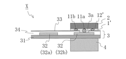
- FIG. 2 shows an example in which the conductive adhesive is applied to a printed wiring board with a reinforcing member.
- the printed wiring board X with a reinforcing member which is an embodiment of the printed wiring board with a reinforcing member, includes a printed wiring board 3 and a conductive adhesive 1'provided on the printed wiring board 3.
- a conductive reinforcing member 2 provided on the conductive adhesive 1'.
- the printed wiring board 3 covers and protects the base member 31, the circuit pattern 32 partially provided on the surface of the base member 31, the insulation protection layer 33 that covers and protects the circuit pattern 32, and the circuit pattern 32. It has an adhesive 34 for adhering the 32 and the base member 31 and the insulating protective layer 33.
- the circuit pattern 32 includes a plurality of signal circuits 32a and a ground circuit 32b.
- the adhesive 34 and the insulating protective layer 33 on the ground circuit 32b are formed with an opening (through hole) 3a that penetrates the adhesive 34 and the insulating protective layer 33 in the thickness direction.
- the conductive adhesive 1' is adhered to the surface of the insulating protective layer 33 of the printed wiring board 3 so as to cover and close the opening 3a, and the binder component (adhesive component) 12'fills the opening 3a. ..
- the conductive adhesive 1' is formed of metal particles (A) 11a and 11b and a binder component (adhesive component) 12'.
- the conductive adhesive 1' has a thick film portion having a relatively thick adhesive and a thin film portion having a relatively thin adhesive. The thick film portion corresponds to the portion filling the opening 3a, and the thin film portion corresponds to the portion located between the insulating protective layer 33 and the reinforcing member 2.
- the metal particles (A) 11a in the thick film portion are located between the reinforcing member 2 and the ground circuit 32b, and preferably contact and conduct the reinforcing member 2 and the ground circuit 32b.
- the thickness of the adhesive in the thick film portion is, for example, 50% or more (preferably 70% or more, more preferably 90%) with respect to the maximum particle diameter of the metal particles (A) 11a in the thick film portion in the adhesive thickness direction. Above).
- the metal particles (A) 11b in the thin film portion are located between the reinforcing member 2 and the insulating protective layer 33, are compressed and deformed by pressure, and are preferably in contact with the reinforcing member 2 and the insulating protective layer 33.
- the thickness of the adhesive in the thin film portion is, for example, 50% or more (preferably 70% or more, more preferably 90% or more) with respect to the maximum particle diameter of the metal particles (A) 11b in the thin film portion in the adhesive thickness direction. Is.
- the gland member 32b and the reinforcing member 2 are electrically connected to each other via the metal particles (A) 11a, the reinforcing member 2 functions as an external connecting conductive layer, and the surface of the reinforcing member 2 is externally grounded. It is electrically connected to the member.
- the metal particles (A) 11 are compressionally deformed, so that they are unlikely to rise on the back side of the base member 31 on which the ground circuit 32b is formed. As a result, when the electronic component 4 is mounted, the adhesion between the printed wiring board 3 and the electronic component 4 is less likely to be hindered. Further, when the metal particles (A) 11a contain a low melting point metal, it is presumed that an alloy is formed at the interface between the gland circuit 32b and the reinforcing member 2 at the time of thermocompression bonding, and the connection stability is better. It becomes.
- the conductive adhesive 1' is, for example, a printed wiring board after the conductive adhesive 1 before flow or before curing, which forms the conductive adhesive 1', is bonded to the surface of the reinforcing member 2 as needed.
- the metal particles (A) 11 are sandwiched between the reinforcing member 2 and the insulating protective layer 33 by adhering them on the insulating protective layer 33 in No. 3 and then flowing or curing the binder component 12 by heating and thermocompression bonding.
- the binder component 12 is allowed to flow to fill the opening 3a while adhering the binder component (adhesive component) 12 to the insulating protective layer 33 while compressing and deforming the metal particles (A) 11b. It can be obtained by curing to form a binder component 12'.
- Both the conductive adhesive 1'and the pre-flow or pre-cured conductive adhesive 1 that forms the conductive adhesive 1' corresponds to the conductive adhesive of the present disclosure.
- the electronic component 4 is connected to the mounting portion provided on the opposite surface of the printed wiring board 3 with respect to the reinforcing member 2.
- the reinforcing member 2 is arranged to face the mounting portion to which the electronic component 4 is connected. As a result, the reinforcing member 2 reinforces the mounting portion of the electronic component 4.
- the conductive reinforcing member 2 is electrically connected to the ground circuit 32b in the printed wiring board 3 via the conductive adhesive 1'. As a result, the reinforcing member 2 is maintained at the same potential as the ground circuit 32, so that noise such as electromagnetic waves from the outside is shielded from the mounting portion of the electronic component 4.
- the conductive adhesive 1' has excellent connection stability between adherends which are conductive members (that is, the reinforcing member 2 and the ground circuit 32b), and the connection stability is maintained even when exposed to a high temperature. Moreover, it is unlikely to cause a ridge on the back side (that is, the surface on which the electronic component 4 is mounted) of the ground circuit 32b and the base member 31, which are adherends. Therefore, when thermocompression bonding is performed to form the conductive adhesive 1', even if the metal particles (A) 11 are pushed in, they are unlikely to rise on the back side of the base member 31 on which the ground circuit 32b is formed. As a result, when the electronic component 4 is mounted, the adhesion between the printed wiring board 3 and the electronic component 4 is less likely to be hindered.
- Example 1 65 parts by mass of bisphenol A type epoxy resin (trade name “jER1256”, manufactured by Mitsubishi Chemical Co., Ltd.) and curing agent (trade name “ST14", Mitsubishi Chemical Co., Ltd.) in toluene so that the solid content is 20% by mass.
- the adhesive composition was prepared by blending 0.05 parts by mass and 35 parts by mass of metal particles with stirring. The properties of the metal particles are as shown in Table 1.
- the obtained adhesive composition was applied to the mold release-treated surface of the PET film whose surface was mold-released, and the solvent was removed by heating to form an anisotropic conductive adhesive.
- Examples 2 to 8 and Comparative Examples 1 to 3 An anisotropic conductive adhesive was prepared in the same manner as in Example 1 except that the types of metal particles in the conductive adhesive and the thickness of the conductive adhesive were changed as shown in Table 1. The properties of the metal particles used in each example are as shown in Table 1, and the ratio in the composition indicates the mass ratio.
- Example 9 35.75 parts by mass of bisphenol A type epoxy resin (trade name “jER1256”, manufactured by Mitsubishi Chemical Co., Ltd.), curing agent (trade name “ST14”, Mitsubishi Chemical) in toluene so that the solid content is 20% by mass. (Manufactured by Co., Ltd.) was blended in an amount of 0.05 parts by mass, silver-coated copper powder (median diameter: 5 ⁇ m) by 29.25 parts by mass, and metal particles by 35 parts by mass, and the mixture was stirred and mixed to prepare an adhesive composition. The properties of the metal particles are as shown in Table 2. The obtained adhesive composition was applied to the mold release-treated surface of the PET film whose surface was mold-released, and the solvent was removed by heating to form an isotropic conductive adhesive.
- Examples 10 to 15 and Comparative Example 4 Isotropic conductivity is the same as in Example 9 except that the types of metal particles (metal particles other than silver-coated copper powder) and the thickness of the conductive adhesive in the conductive adhesive are changed as shown in Table 2. An adhesive was made. The properties of the metal particles used in each example are as shown in Table 2, and the ratio in the composition indicates the mass ratio.
- the median diameter of the metal particles was measured using a flow-type particle image analyzer (trade name “FPIA-3000”, manufactured by Sysmex Corporation). Specifically, the measurement was performed with a metal particle dispersion adjusted to a concentration of 4000 to 20000 pieces / ⁇ l in the LPF measurement mode in a bright field optical system using a 10x objective lens.
- the above metal particle dispersion is prepared by adding 0.1 to 0.5 ml of a surfactant to an aqueous solution of sodium hexametaphosphate adjusted to 0.2% by mass and adding 0.1 ⁇ 0.01 g of metal particles as a measurement sample. did.
- the suspension in which the metal particles were dispersed was subjected to a dispersion treatment for 1 to 3 minutes with an ultrasonic disperser and used for measurement.
- the median diameters of the metal particles obtained by the measurement are shown in Tables 1 and 2.
- the 20% compressive strength under 170 ° C environment was measured according to JIS Z 8844: 2019. Specifically, using a microcompression tester (model "MCT-510", manufactured by Shimadzu Corporation), the tip terminal is ⁇ 50 ⁇ m, and the test speed is 4 mN / sec to 15 mN / sec (particles) in an environment of 170 ° C. (Change as appropriate depending on the hardness of).
- the printed wiring board has two copper foil patterns (thickness: 18 ⁇ m, line width: 3 mm) extending in parallel at intervals on a base member made of a polyimide film having a thickness of 12.5 ⁇ m.
- the insulating protective layer has an insulating protective layer (thickness: 25 ⁇ m) made of an insulating adhesive (thickness: 13 ⁇ m) and a polyimide having a thickness of 25 ⁇ m.
- a cylindrical opening (diameter: 1 mm) that exposes each copper foil pattern is provided. When the conductive adhesive and the printed wiring board were overlapped, this opening was completely covered with the conductive adhesive. Then, the electric resistance value between the obtained copper foil pattern of the evaluation board and the SUS plate is measured using a resistance meter, and the resistance value (initial resistance value) between the printed wiring board and the SUS plate before reflow is used. did.
- Circularity 4 ⁇ ⁇ (area) / (perimeter) 2
- the conductive adhesive of the embodiment has a small initial resistance value, excellent connection stability between adherends which are conductive members, a large circularity, and is unlikely to cause bulging to the back side of the adherend. rice field.
- the resistance value and the rate of change in resistance value after reflow were small, and it was evaluated that good conductivity was maintained even when exposed to high temperatures.
- the 20% compressive strength was high in an environment of 170 ° C. (Comparative Examples 1 to 4)
- a ridge was generated on the back side of the adherend, and the circularity could not be measured.
- Comparative Examples 1 and 2 the shape of the circle to be measured for the circularity is deformed due to the bulge on the back side of the adherend, and the measurement is impossible.
- Comparative Examples 3 and 4 the cover is covered. Due to the large number of ridges on the back side of the body, it was not possible to recognize the circle to be measured for the circularity, and it was impossible to measure. Further, as compared with Example 1 and Example 2, when the content ratio of tin in the metal particles (A) was high, the rate of change in resistance value was lower.
Landscapes
- Chemical & Material Sciences (AREA)
- Organic Chemistry (AREA)
- Engineering & Computer Science (AREA)
- Microelectronics & Electronic Packaging (AREA)
- Manufacturing & Machinery (AREA)
- Inorganic Chemistry (AREA)
- Adhesives Or Adhesive Processes (AREA)
- Conductive Materials (AREA)
- Health & Medical Sciences (AREA)
- Chemical Kinetics & Catalysis (AREA)
- Medicinal Chemistry (AREA)
- Polymers & Plastics (AREA)
Abstract
導電部材である被着体同士の接続安定性に優れ、高温に付された場合であっても接続安定性が維持され、且つ被着体の裏側への隆起が起こりにくい導電性接着剤を提供する。 導電性接着剤1は、バインダー成分12と、170℃環境下での20%圧縮強度が25MPa以下である金属粒子(A)11とを含む。金属粒子11は融点280℃以下の金属を含むことが好ましい。金属粒子(A)11中の融点280℃以下の金属の含有割合は80質量%以上であることが好ましい。
Description
本開示は、導電性接着剤に関する。
プリント配線板は、携帯電話、ビデオカメラ、ノートパソコンなどの電子機器において、機構の中に回路を組み込むために多用されている。また、プリンタヘッドのような可動部と制御部との接続にも利用されている。これらの電子機器では、電磁波シールド対策が必須となっており、装置内で使用されるプリント配線板においても、電磁波シールド対策を施したシールドプリント配線板が用いられている。
上記シールドプリント配線板としては、例えば、プリント回路を含む基体フィルム上に、接着剤(接着剤層)、金属薄膜、および絶縁層がこの順に積層した電磁波シールドフィルムの接着剤面が密着するように上記電磁波シールドフィルムを載置し、その後加熱・加圧(熱圧着)により上記接着剤が上記基体フィルムに接着した構造を有する。
上記プリント配線板は電子部品を実装して使用される。プリント配線板には、屈曲可能なフレキシブルプリント配線板(FPC)が知られている。FPCに使用されるプリント配線板は、電子部品を実装した部位が折れ曲がることで電子部品が脱落しやすくなるため、これを防止する目的でプリント配線板上に補強部材が設けられることがある。上記補強部材には、プリント配線板内に侵入あるいは生じた電磁波を外部に逃がすことを目的として、外部電位と接地可能な導電性を備える補強部材が用いられることがある。例えば、特許文献1には、導電性を有する補強部材と導電性接着剤を備える補強部材付きプリント配線板が開示されている。
従来の補強部材付きプリント配線板に用いられる導電性接着剤(導電性接着シート)としては、グランド回路と接地側の補強部材との導電性に優れる等方導電性接着剤が多用されている。等方導電性接着剤は導電性粒子を多量含むものであるが、経済的な観点から導電性接着剤に用いられる導電性粒子の量は少ない方が好ましい。
しかしながら、特許文献1に開示されたプリント配線板のように、プリント配線板表面の絶縁層に設けられた開口部を覆うように導電性接着剤を熱圧着により貼り合わせて使用する場合、導電性接着剤中の導電性粒子が少量である異方導電性接着剤では、開口部内に充填される導電性粒子の量が不足し、グランド回路と接地側の補強部材との導電性が低下し、接続安定性が劣る傾向となる。また、初期の接続安定性が良好である場合であっても、リフロー工程等において高温に付された際、導電性が低下する場合があった。
また、導電性を向上させる目的で、導電性粒子として粒子径の大きい粒子や樹枝状粒子を用いることが考えられる。しかしながら、従来の導電性接着剤においてこれらの粒子を用いた場合、上記熱圧着により粒子が押し込まれてグランド回路が形成されたベース部材の裏側に隆起してベース部材の平滑性が損なわれるため、その後にベース部材上に部品実装する際に密着性の妨げになる場合がある。
従って、本開示の目的は、導電部材である被着体同士の接続安定性に優れ、高温に付された場合であっても接続安定性が維持され、且つ被着体の裏側への隆起が起こりにくい導電性接着剤を提供することにある。
本開示は、バインダー成分と、170℃環境下での20%圧縮強度が25MPa以下である金属粒子とを含む、導電性接着剤を提供する。
上記金属粒子の170℃環境下での20%圧縮強度は1MPa以上であってもよい。
上記金属粒子は融点300℃以下の金属を含むことが好ましい。
上記金属粒子中の上記融点300℃以下の金属の含有割合は80質量%以上であることが好ましい。
上記金属粒子の含有割合は10~70質量%であることが好ましい。
上記金属粒子は、構成金属として錫および錫よりも融点が高い金属を含むことが好ましい。
上記錫よりも融点が高い金属は、ビスマス、インジウム、金、銀、銅、白金、ニッケル、パラジウム、またはアンチモンを含んでいてもよい。
上記金属粒子は球状であることが好ましい。
上記金属粒子のメディアン径は1~50μmであることが好ましい。
上記金属粒子は錫含有合金粒子を含むことが好ましい。
上記導電性接着剤はプリント配線板用であることが好ましい。
上記金属粒子は一部が接着剤から突出しており、上記接着剤の厚さは上記金属粒子のメディアン径に対して10~30%であることが好ましい。
上記導電性接着剤は厚膜部および薄膜部を有し、
上記厚膜部における接着剤の厚さは当該厚膜部における上記金属粒子の接着剤厚さ方向の最大粒子径に対して50%以上であり、
上記薄膜部における接着剤の厚さは当該薄膜部における上記金属粒子の接着剤厚さ方向の最大粒子径に対して50%以上であるものであってもよい。
上記厚膜部における接着剤の厚さは当該厚膜部における上記金属粒子の接着剤厚さ方向の最大粒子径に対して50%以上であり、
上記薄膜部における接着剤の厚さは当該薄膜部における上記金属粒子の接着剤厚さ方向の最大粒子径に対して50%以上であるものであってもよい。
また、本開示は、プリント配線板と、上記プリント配線板上に設けられた上記導電性接着剤と、上記導電性接着剤上に設けられた、導電性を有する補強部材と、を備え、
上記プリント配線板は、ベース部材と、上記ベース部材の表面に部分的に設けられた回路パターンと、上記回路パターンを覆い絶縁保護する絶縁保護層と、上記回路パターンを覆い且つ上記回路パターンおよび上記ベース部材と上記絶縁保護層とを接着するための接着剤と、を有し、
上記回路パターンは、複数の信号回路およびグランド回路を含み、
上記グランド回路上の上記接着剤および上記絶縁保護層には、上記接着剤および上記絶縁保護層を厚さ方向に貫通する開口部が形成されており、
上記導電性接着剤は上記プリント配線板の上記絶縁保護層表面に、上記開口部を覆い塞ぐように接着されており、上記導電性接着剤の厚膜部は上記開口部を充填している、補強部材付きプリント配線板を提供する。
上記厚膜部において、上記金属粒子は上記補強部材および上記グランド回路と接触しており、上記薄膜部において、上記金属粒子は上記補強部材および上記絶縁保護層と接触していることが好ましい。
本開示の導電性接着剤は、導電部材である被着体同士の接続安定性に優れ、高温に付された場合であっても接続安定性が維持され、且つ被着体の裏側への隆起が起こりにくい。このため、例えば、グランド回路と接地側の補強部材との接着に使用した際、グランド回路と接地側の補強部材との接続安定性に優れ、且つグランド回路が形成されたベース部材の裏側への隆起が起こりにくい。また、このような効果は、金属粒子等の導電性粒子の配合量が多い場合はもちろん、少ない場合であっても上記効果を奏し、経済的にも優れる。
[導電性接着剤]
本開示の導電性接着剤は、バインダー成分と、170℃環境下での20%圧縮強度が25MPa以下である金属粒子とを少なくとも含む。上記バインダー成分および上記金属粒子は、それぞれ、一種のみを使用してもよいし、二種以上を使用してもよい。なお、本明細書において、上記170℃環境下での20%圧縮強度が25MPa以下である金属粒子を「金属粒子(A)」と称する場合がある。上記導電性接着剤は、金属粒子(A)以外のその他の導電性粒子を含んでいてもよい。
本開示の導電性接着剤は、バインダー成分と、170℃環境下での20%圧縮強度が25MPa以下である金属粒子とを少なくとも含む。上記バインダー成分および上記金属粒子は、それぞれ、一種のみを使用してもよいし、二種以上を使用してもよい。なお、本明細書において、上記170℃環境下での20%圧縮強度が25MPa以下である金属粒子を「金属粒子(A)」と称する場合がある。上記導電性接着剤は、金属粒子(A)以外のその他の導電性粒子を含んでいてもよい。
上記導電性接着剤は、異方導電性接着剤であってもよく、等方導電性接着剤であってもよい。例えば、金属粒子(A)が導電性接着剤において主に導電性を担う場合は異方導電性接着剤となり、金属粒子(A)とその他の導電性粒子(例えば後述の金属粒子(B))とをバランス良く配合する場合は等方導電性接着剤となる。
図1に、本開示の導電性接着剤(接着剤層)の一実施形態を示す。導電性接着剤1は、層状(シート状)であり、バインダー成分12と、金属粒子(A)11とを含む。金属粒子(A)11は、バインダー成分12から構成される接着剤の表面から突出している。
(金属粒子(A))
上記金属粒子(A)は導電性を有する。これにより、上記導電性接着剤は導電性を備えることとなる。上記金属粒子(A)の170℃環境下での20%圧縮強度は、25MPa以下であり、好ましくは23MPa以下、より好ましくは22MPa以下である。上記20%圧縮強度が25MPa以下であることにより、170℃環境下において高圧力を付された際、金属粒子(A)は圧縮変形しやすく、金属粒子(A)が押し込まれても被着体の裏側に隆起しにくい。上記金属粒子(A)の20%圧縮強度は、JIS Z 8844:2019に準拠して測定される。
上記金属粒子(A)は導電性を有する。これにより、上記導電性接着剤は導電性を備えることとなる。上記金属粒子(A)の170℃環境下での20%圧縮強度は、25MPa以下であり、好ましくは23MPa以下、より好ましくは22MPa以下である。上記20%圧縮強度が25MPa以下であることにより、170℃環境下において高圧力を付された際、金属粒子(A)は圧縮変形しやすく、金属粒子(A)が押し込まれても被着体の裏側に隆起しにくい。上記金属粒子(A)の20%圧縮強度は、JIS Z 8844:2019に準拠して測定される。
上記金属粒子(A)の170℃環境下での20%圧縮強度は、1.0MPa以上であってもよく、5.0MPa以上、11MPa以上であってもよい。上記20%圧縮強度が1.0MPa以上であると、170℃環境下において高圧力を付された際に金属粒子(A)が圧縮されすぎず、粒子形状を維持することができ、被着体同士の接続安定性により優れる。このような効果は、上記導電性接着剤が異方導電性接着剤である場合において特に発揮される。
上記金属粒子(A)は、構成金属として、融点が280℃以下の金属を少なくとも含むことが好ましい。上記融点が280℃以下の金属としては、例えば、錫、ビスマス、インジウム、およびこれらの合金などが挙げられる。中でも、構成金属として錫を含むことが好ましい。上記融点が280℃以下の金属は、一種のみを使用してもよく、二種以上を使用してもよい。また、上記金属粒子(A)は上述した金属の合金であってもよい。なお、本明細書において、上記融点が280℃以下の金属を「低融点金属」と称する場合がある。
上記金属粒子(A)中の上記低融点金属の含有割合は、上記金属粒子(A)の総量100質量%に対して、80質量%以上であることが好ましく、より好ましくは85質量%以上、さらに好ましくは90質量%以上、特に好ましくは94質量%以上である。上記金属粒子(A)中の低融点金属は、熱圧着時に導電性を有する被着体(グランド回路や接地側の補強部材など)とで界面に合金を形成するものと推測される。このため、上記金属粒子(A)低融点金属を80質量%以上(特に、90質量%以上)含むと、リフロー工程等において高温に付された際も良好な導電性が維持される。上記含有割合は、100質量%であってもよく、99.9質量%以下、99.6質量%以下であってもよい。上記含有割合が99.9質量%以下であると、金属粒子(A)がある程度の硬さを有し、170℃環境下において高圧力を付された際に金属粒子(A)が圧縮されすぎず、被着体同士の導通を確保することが容易となる。このような効果は、上記導電性接着剤が異方導電性接着剤である場合に特に発揮される。
上記金属粒子(A)は、上記低融点金属として錫を含むことが好ましい。上記金属粒子(A)中の錫の含有割合は、上記金属粒子(A)の総量100質量%に対して、30質量%以上であることが好ましく、より好ましくは40質量%以上である。上記金属粒子(A)中の錫の含有割合は、80質量%以上、90質量%以上、94質量%以上であってもよい。上記金属粒子(A)が錫を30質量%以上含むと、リフロー工程等において高温に付された際も良好な導電性が維持される。また、上記導電性接着剤層が異方導電性接着剤である場合、上記金属粒子(A)が錫を80質量%以上(特に、90質量%以上)含むと、このような効果がより優れる。上記含有割合は、99.9質量%以下が好ましく、より好ましくは99.6質量%以下である。上記含有割合が99.9質量%以下であると、金属粒子(A)がある程度の硬さを有し、170℃環境下において高圧力を付された際に金属粒子(A)が圧縮されすぎず、被着体同士の導通を確保することが容易となる。
上記金属粒子(A)は、接続安定性により優れる観点から、構成金属として、上記低融点金属以外の金属(すなわち、融点が300℃超の金属)を含んでいてもよい。このような金属としては、金、銀、銅、白金、ニッケル、亜鉛、鉛、パラジウム、アンチモン、およびこれらの合金などが挙げられる。中でも、金、銀、銅、白金、ニッケル、パラジウムが好ましい。上記金属はそれぞれ一種のみを含んでいてもよいし、二種以上を含んでいてもよい。また、上記金属粒子(A)は上述した金属の合金であってもよい。
上記金属粒子(A)は、構成金属として錫を含む場合、さらに錫以外のその他の金属を含んでいてもよい。上記その他の金属としては、金、銀、銅、白金、ニッケル、亜鉛、鉛、パラジウム、ビスマス、アンチモン、インジウム、およびこれらの合金などが挙げられる。上記金属粒子(A)は、接続安定性により優れる観点から、上記その他の金属として、ビスマス、インジウム、金、銀、銅、白金、ニッケル、パラジウム、アンチモン等の、錫よりも融点が高い(または硬い)金属を含むことが好ましい。上記その他の金属はそれぞれ一種のみを含んでいてもよいし、二種以上を含んでいてもよい。また、上記金属粒子(A)は上述した金属の合金であってもよい。
上記金属粒子(A)としては、具体的には、例えば、銅粒子、銀粒子、ニッケル粒子、銀被覆銅粒子、インジウム粒子、錫粒子、鉛粒子、ビスマス粒子、錫含有合金粒子、金被覆銅粒子、銀被覆ニッケル粒子、金被覆ニッケル粒子、インジウム被覆銅粒子、錫被覆銅粒子、鉛被覆銅粒子、錫被覆ニッケル粒子、錫被覆合金粒子、金被覆錫粒子、銀被覆錫粒子、ビスマス被覆銅粒子、インジウム被覆ニッケル粒子、ビスマス被覆ニッケル粒子、錫ビスマス合金粒子、銀被覆合金粒子などが挙げられる。上記金属粒子(A)は、電解法、アトマイズ法、還元法などにより作製することができる。
上記金属粒子(A)の形状としては、球状(真球状、楕球状など)、フレーク状(鱗片状)、樹枝状、繊維状、不定形(多面体)などが挙げられる。中でも、金属粒子(A)が押し込まれても被着体の裏側に、より隆起しにくい観点から、球状が好ましい。
上記金属粒子(A)のメディアン径(D50)は、1~50μmであることが好ましく、より好ましくは10~45μmである。上記メディアン径が1μm以上であると、導電性がより良好となる。また、金属粒子(A)の分散性が良好で凝集が抑制できる。上記平均粒径が50μm以下であると、金属粒子(A)が押し込まれても被着体の裏側に、より隆起しにくい。
上記導電性接着剤における金属粒子(A)の含有割合は、導電性接着剤の総量100質量%に対して、10~70質量%であることが好ましく、より好ましくは15~60質量%、さらに好ましくは20~50質量%である。上記含有割合が10質量%以上であると、導電性がより良好となる。上記含有割合が70質量%以下であると、経済的に優れ、また、金属粒子(A)が押し込まれても被着体の裏側に隆起しにくい。
(その他の導電性粒子)
上記その他の導電性粒子としては、金属粒子(A)以外の公知乃至慣用の導電性粒子を用いることができる。上記その他の導電性粒子としては、例えば、金属粒子、金属被覆樹脂粒子、金属繊維、カーボンフィラー、カーボンナノチューブなどが挙げられる。中でも、金属粒子(すなわち、170℃環境下での20%圧縮強度が25MPa超である金属粒子)が好ましい。上記金属粒子を金属粒子(A)と組み合わせて用いると、金属粒子(A)の170℃における圧縮強度が1MPa未満と低い場合であっても、170℃環境下において高圧力を付された際に金属粒子(A)が圧縮されすぎず、粒子形状を維持することができ、被着体同士の接続安定性により優れる。上記その他の導電性粒子は、一種のみを使用してもよいし、二種以上を使用してもよい。なお、本明細書において、上記170℃環境下での20%圧縮強度が25MPa超である金属粒子を「金属粒子(B)」と称する場合がある。
上記その他の導電性粒子としては、金属粒子(A)以外の公知乃至慣用の導電性粒子を用いることができる。上記その他の導電性粒子としては、例えば、金属粒子、金属被覆樹脂粒子、金属繊維、カーボンフィラー、カーボンナノチューブなどが挙げられる。中でも、金属粒子(すなわち、170℃環境下での20%圧縮強度が25MPa超である金属粒子)が好ましい。上記金属粒子を金属粒子(A)と組み合わせて用いると、金属粒子(A)の170℃における圧縮強度が1MPa未満と低い場合であっても、170℃環境下において高圧力を付された際に金属粒子(A)が圧縮されすぎず、粒子形状を維持することができ、被着体同士の接続安定性により優れる。上記その他の導電性粒子は、一種のみを使用してもよいし、二種以上を使用してもよい。なお、本明細書において、上記170℃環境下での20%圧縮強度が25MPa超である金属粒子を「金属粒子(B)」と称する場合がある。
上記金属粒子(B)を構成する金属としては、上述の金属粒子(A)を構成する金属として例示および説明されたものが挙げられる。上記金属は一種のみを使用してもよいし、二種以上を使用してもよい。
上記金属粒子(B)としては、具体的には、例えば、銅粒子、銀粒子、ニッケル粒子、銀被覆銅粒子、インジウム粒子、錫粒子、鉛粒子、ビスマス粒子、金被覆銅粒子、銀被覆ニッケル粒子、金被覆ニッケル粒子、インジウム被覆銅粒子、錫被覆銅粒子、鉛被覆銅粒子、ビスマス被覆銅粒子、インジウム被覆ニッケル粒子、錫被覆ニッケル粒子、ビスマス被覆ニッケル粒子、銀被覆合金粒子などが挙げられる。上記銀被覆合金粒子としては、例えば、銅を含む合金粒子(例えば、銅とニッケルと亜鉛との合金からなる銅合金粒子)が銀により被覆された銀被覆銅合金粒子などが挙げられる。金属粒子(B)としては、中でも、銀粒子、銀被覆銅粒子、銀被覆銅合金粒子が好ましい。導電性に優れ、導電性粒子の酸化および凝集を抑制し、且つ導電性粒子のコストを下げることができる観点から、特に、銀被覆銅粒子、銀被覆銅合金粒子が好ましい。
金属粒子(B)の形状としては、球状(真球状、楕球状など)、フレーク状(鱗片状、扁平状)、樹枝状(デンドライト状)、繊維状、不定形(多面体)などが挙げられる。中でも、フレーク状、樹枝状が好ましい。この理由は、次のためである。金属粒子(B)の形状を、フレーク状、樹枝状にすることで、金属粒子(B)同士が重なり合った姿勢をとりやすく、これによって、金属粒子(B)同士の接触が増え、平面方向の導電性が向上する。この平面方向の導電性の向上と、金属粒子(A)による厚さ方向の導電性が相まって、導電性接着剤全体の導電性が向上(電気的に安定)し、被着体同士の接続安定性をより向上させることができる。
金属粒子(B)のメディアン径(D50)は、0.5~25μmであることが好ましく、より好ましくは3~10μmである。上記メディアン径が0.5μm以上であると、被着体同士の接続安定性がより優れる。また、金属粒子(B)の分散性が良好で凝集が抑制できる。上記メディアン径が25μm以下であると、導電性接着剤の被着体への密着強度により優れる。
上記導電性接着剤中の金属粒子(B)の含有割合は、導電性接着剤の総量100質量%に対して、10~70質量%であることが好ましく、より好ましくは15~60質量%、さらに好ましくは20~50質量%である。上記含有割合が10質量%以上であると、導電性接着剤の平面方向の導電性がより発揮され、被着体同士の接続安定性により優れる。上記含有割合が70質量%以下であると、導電性接着剤層の柔軟性に優れる。
(バインダー成分)
上記バインダー成分としては、熱可塑性樹脂、熱硬化型樹脂、活性エネルギー線硬化型化合物などが挙げられる。上記熱可塑性樹脂としては、例えば、ポリスチレン系樹脂、酢酸ビニル系樹脂、ポリエステル系樹脂、ポリオレフィン系樹脂(例えば、ポリエチレン系樹脂、ポリプロピレン系樹脂組成物等)、ポリイミド系樹脂、アクリル系樹脂などが挙げられる。上記熱可塑性樹脂は、一種のみを使用してもよいし、二種以上を使用してもよい。
上記バインダー成分としては、熱可塑性樹脂、熱硬化型樹脂、活性エネルギー線硬化型化合物などが挙げられる。上記熱可塑性樹脂としては、例えば、ポリスチレン系樹脂、酢酸ビニル系樹脂、ポリエステル系樹脂、ポリオレフィン系樹脂(例えば、ポリエチレン系樹脂、ポリプロピレン系樹脂組成物等)、ポリイミド系樹脂、アクリル系樹脂などが挙げられる。上記熱可塑性樹脂は、一種のみを使用してもよいし、二種以上を使用してもよい。
上記熱硬化型樹脂としては、熱硬化性を有する樹脂(熱硬化性樹脂)および上記熱硬化性樹脂を硬化して得られる樹脂の両方が挙げられる。上記熱硬化性樹脂としては、例えば、フェノール系樹脂、エポキシ系樹脂、ウレタン系樹脂、メラミン系樹脂、アルキド系樹脂などが挙げられる。上記熱硬化型樹脂は、一種のみを使用してもよいし、二種以上を使用してもよい。
上記エポキシ系樹脂としては、例えば、ビスフェノール型エポキシ系樹脂、スピロ環型エポキシ系樹脂、ナフタレン型エポキシ系樹脂、ビフェニル型エポキシ系樹脂、テルペン型エポキシ系樹脂、グリシジルエーテル型エポキシ系樹脂、グリシジルアミン型エポキシ系樹脂、ノボラック型エポキシ系樹脂などが挙げられる。
上記ビスフェノール型エポキシ樹脂としては、例えば、ビスフェノールA型エポキシ樹脂、ビスフェノールF型エポキシ樹脂、ビスフェノールS型エポキシ樹脂、テトラブロムビスフェノールA型エポキシ樹脂などが挙げられる。上記グリシジルエーテル型エポキシ樹脂としては、例えば、トリス(グリシジルオキシフェニル)メタン、テトラキス(グリシジルオキシフェニル)エタンなどが挙げられる。上記グリシジルアミン型エポキシ樹脂としては、例えばテトラグリシジルジアミノジフェニルメタンなどが挙げられる。上記ノボラック型エポキシ樹脂としては、例えば、クレゾールノボラック型エポキシ樹脂、フェノールノボラック型エポキシ樹脂、α-ナフトールノボラック型エポキシ樹脂、臭素化フェノールノボラック型エポキシ樹脂などが挙げられる。
上記活性エネルギー線硬化型化合物は、活性エネルギー線照射により硬化し得る化合物(活性エネルギー線硬化性化合物)および上記活性エネルギー線硬化性化合物を硬化して得られる化合物の両方が挙げられる。活性エネルギー線硬化性化合物としては、特に限定されないが、例えば、分子中に1個以上(好ましくは2個以上)のラジカル反応性基(例えば、(メタ)アクリロイル基)を有する重合性化合物などが挙げられる。上記活性エネルギー線硬化型化合物は、一種のみを使用してもよいし、二種以上を使用してもよい。
上記バインダー成分としては、中でも、熱硬化型樹脂が好ましい。この場合、導電性接着剤をプリント配線板や、電磁波シールド対策を施したシールドプリント配線板などの被着体上に配置した後、加圧および加熱によりバインダー成分を硬化させることができ、貼り付け部の接着性が良好となる。例えば、バインダー成分を熱硬化性樹脂とした場合、熱圧着後におけるバインダー成分は、上記熱硬化性樹脂が硬化した熱硬化型樹脂となる。
上記バインダー成分が熱硬化型樹脂を含む場合、上記バインダー成分を構成する成分として、熱硬化反応を促進するための硬化剤を含んでいてもよい。上記硬化剤は、上記熱硬化性樹脂の種類に応じて適宜選択することができる。上記硬化剤は、一種のみを使用してもよいし、二種以上を使用してもよい。
上記導電性接着剤におけるバインダー成分の含有割合は、特に限定されないが、接着剤の総量100質量%に対して、15~95質量%が好ましく、より好ましくは20~90質量%、さらに好ましくは30~80質量%である。上記含有割合が15質量%以上であると、被着体に対する密着性がより良好となる。上記含有割合が95質量%以下であると、金属粒子(A)を充分に配合することができ、導電性により優れる。
上記導電性接着剤は、本開示が目的とする効果を損なわない範囲内において、上記の各成分以外のその他の成分を含有していてもよい。上記その他の成分としては、公知乃至慣用の接着剤に含まれる成分が挙げられる。上記その他の成分としては、例えば、硬化促進剤、可塑剤、難燃剤、消泡剤、粘度調整剤、酸化防止剤、希釈剤、沈降防止剤、充填剤、着色剤、レベリング剤、カップリング剤、紫外線吸収剤、粘着付与樹脂、ブロッキング防止剤などが挙げられる。上記その他の成分は、一種のみを使用してもよいし、二種以上を使用してもよい。
上記導電性接着剤の厚さは、2~20μmであることが好ましく、より好ましくは3~17μmである。上記厚さが2μm以上であると、被着体に対する接着力がより良好となる。上記厚さが20μm以下であると、コストを抑えることができ、また上記導電性接着剤を備えた製品を薄く設計することができる。なお、上記金属粒子(A)の一部が上記導電性接着剤から突出している場合の導電性接着剤の厚さは、金属粒子(A)が突出していない領域における厚さである。また、加熱等により導電性接着剤を構成する接着剤成分(バインダー成分)が流動して被着体に形成された開口部内に侵入した場合などにおける導電性接着剤の厚さは、上記開口部内に侵入していない領域における接着剤の厚さである。
上記金属粒子(A)は一部が上記導電性接着剤から突出していてもよい。例えば、流動前あるいは硬化前における上記導電性接着剤においては、上記金属粒子(A)は一部が上記導電性接着剤から突出していることが好ましい。この場合、上記導電性接着剤(金属粒子(A)が突出していない領域)の厚さは上記金属粒子(A)のメディアン径に対して、10~30%であることが好ましく、より好ましくは12~25%である。上記厚さが10%以上であると、被着体に対する接着性がより優れる。上記厚さが30%以下であると、上記金属粒子(A)が上記導電性接着剤から突出する割合が大きく、流動後あるいは硬化後において厚膜部が形成された際、厚膜部において接着される被着体同士の導通を確保することが容易となる。
上記導電性接着剤について、下記導電性試験により求められる抵抗値(初期抵抗値)は、特に限定されないが、150mΩ以下であることが好ましく、より好ましくは130mΩ以下、さらに好ましくは100mΩ以下、特に好ましくは80mΩ以下である。上記初期抵抗値が150mΩ以下であると、上記導電性接着剤を介した被着体同士の導通が良好となる。
[導電性試験]
導電性接着剤を、SUS板(厚さ:200μm)に、温度:120℃、圧力:0.5MPaの条件で5秒間加熱加圧して貼り合わせ、導電性接着剤側の面を評価用のプリント配線板上に貼り合わせ、プレス機を用いて、60秒間真空引きした後、温度:170℃、圧力:3.0MPaの条件で30分間加熱加圧して、評価用基板を準備する。プリント配線板として、厚さ12.5μmのポリイミドフィルムからなるベース部材の上に、グランド回路を疑似した2本の銅箔パターン(厚さ:18μm、線幅:3mm)が形成され、その上に絶縁性の接着剤(厚さ:13μm)および厚さ25μmのポリイミドフィルムからなるカバーレイが形成されたプリント配線板を用いる。カバーレイには、直径1mmのグランド接続部を模擬した円形開口部が形成されている。上記評価用基板について、銅箔パターンとSUS板の間の電気抵抗値を抵抗計で測定して抵抗値とする。
上記導電性接着剤について、265℃の熱風に5秒間曝されるような温度プロファイルに設定したリフロー工程を5サイクル通過させた後の、導電性試験により求められる抵抗値(リフロー後抵抗値)は、特に限定されないが、150mΩ以下であることが好ましく、より好ましくは50mΩ以下、さらに好ましくは30mΩ以下である。上記抵抗値が150mΩ以下であると、上記導電性接着剤を介した被着体同士の導通が良好となる。なお、上記リフロー後抵抗値は、上記リフロー工程を5サイクル通過させた後の上記評価用基板について、上記初期抵抗値の導電性試験と同様にして測定される。
上記導電性接着剤について、抵抗値変化率[(リフロー後抵抗値-初期抵抗値)/初期抵抗値×100]は、特に限定されないが、80%以下が好ましく、より好ましくは50%以下、さらに好ましくは10%以下、さらに好ましくは0%以下、特に好ましくは-20%以下である。上記抵抗値変化率が80%以下であると、高温に付された場合であっても接続抵抗値の上昇が起こりにくく、導電部材である被着体同士の接続安定性がより優れたものとなる。
上記導電性接着剤について、円形度測定により求められる円形度は、特に限定されないが、0.7以上が好ましく、より好ましくは0.75以上、さらに好ましくは0.8以上である。上記円形度が0.7以上であると、被着体の裏側への隆起が小さく、評価用基板を適用したプリント配線板を部品実装する際に密着性の妨げになりにくい。上記円形度は、上記導電性評価にて作製された上記評価用基板の開口部(直径1mm)の裏面の形状に基づき、以下の式より求められる。
円形度=4π×(面積)/(周囲長)2
円形度=4π×(面積)/(周囲長)2
上記導電性接着剤は、プリント配線板用途であることが好ましく、フレキシブルプリント配線板(FPC)用途であることが特に好ましい。上記導電性接着剤は、導電部材である被着体同士の接続安定性に優れ、高温に付された場合であっても接続安定性が維持され、且つ被着体の裏側への隆起が起こりにくい。また、このような効果は、金属粒子等の導電性粒子の配合量が多い場合はもちろん、少ない場合であっても上記効果を奏し、経済的にも優れる。従って、上記導電性接着剤は、プリント配線板用(特に、FPC用)の電磁波シールドフィルム、導電性ボンディングフィルムとして好ましく使用することができる。上記導電性ボンディングフィルムは、プリント配線板への導電性(金属)補強板の取付けを目的としたものであり、プリント配線板内に侵入あるいは生じた電磁波を外部に逃がすことを目的としたグランド接続引き出しフィルムも挙げられる。
上記導電性接着剤は、少なくとも一方の面にセパレートフィルムが積層されていてもよい。すなわち、上記導電性接着剤は、セパレートフィルムと、当該セパレートフィルムの離型面に形成された上記導電性接着剤とを備える積層体として提供されてもよい。上記セパレートフィルムは使用時に剥離される。
上記導電性接着剤は、公知乃至慣用の製造方法により製造することができる。例えば、セパレートフィルムなどの仮基材または基材上に、導電性接着剤を形成する接着剤組成物を塗布(塗工)し、必要に応じて、脱溶媒および/または一部硬化させて形成することが挙げられる。
上記接着剤組成物は、例えば、上述の導電性接着剤に含まれる各成分に加え、溶剤(溶媒)を含む。溶剤としては、例えば、トルエン、アセトン、メチルエチルケトン、メタノール、エタノール、プロパノール、ジメチルホルムアミドなどが挙げられる。接着剤組成物の固形分濃度は、形成する導電性接着剤の厚さなどに応じて適宜設定される。
上記接着剤組成物の塗布には、公知のコーティング法が用いられてもよい。例えば、グラビアロールコーター、リバースロールコーター、キスロールコーター、リップコーターディップロールコーター、バーコーター、ナイフコーター、スプレーコーター、コンマコーター、ダイレクトコーター、スロットダイコーターなどのコーターが用いられてもよい。
[補強部材付きプリント配線板]
図2に、上記導電性接着剤を補強部材付きプリント配線板に適用した例を示す。図2に示すように、補強部材付きプリント配線板の一実施形態である補強部材付きプリント配線板Xは、プリント配線板3と、プリント配線板3上に設けられた導電性接着剤1’と、導電性接着剤1’上に設けられた、導電性を有する補強部材2と、を備える。
図2に、上記導電性接着剤を補強部材付きプリント配線板に適用した例を示す。図2に示すように、補強部材付きプリント配線板の一実施形態である補強部材付きプリント配線板Xは、プリント配線板3と、プリント配線板3上に設けられた導電性接着剤1’と、導電性接着剤1’上に設けられた、導電性を有する補強部材2と、を備える。
プリント配線板3は、ベース部材31と、ベース部材31の表面に部分的に設けられた回路パターン32と、回路パターン32を覆い絶縁保護する絶縁保護層33と、回路パターン32を覆い且つ回路パターン32およびベース部材31と絶縁保護層33とを接着するための接着剤34と、を有する。回路パターン32は、複数の信号回路32aおよびグランド回路32bを含む。グランド回路32b上の接着剤34および絶縁保護層33には、接着剤34および絶縁保護層33を厚さ方向に貫通する開口部(スルーホール)3aが形成されている。
導電性接着剤1’はプリント配線板3の絶縁保護層33表面に、開口部3aを覆い塞ぐように接着されており、バインダー成分(接着剤成分)12’は開口部3aを充填している。導電性接着剤1’は金属粒子(A)11a、11bとバインダー成分(接着剤成分)12’とから形成されている。導電性接着剤1’は、接着剤の厚さが比較的厚い厚膜部と、接着剤の厚さが比較的薄い薄膜部とを有する。厚膜部は開口部3aを充填している部分と一致し、薄膜部は絶縁保護層33と補強部材2との間に位置する部分と一致する。厚膜部における金属粒子(A)11aは、補強部材2とグランド回路32bの間に位置し、補強部材2とグランド回路32bとを好ましくは接触して導通する。厚膜部における接着剤の厚さは当該厚膜部における金属粒子(A)11aの接着剤厚さ方向の最大粒子径に対して例えば50%以上(好ましくは70%以上、より好ましくは90%以上)である。薄膜部における金属粒子(A)11bは、補強部材2と絶縁保護層33の間に位置し、圧力によって圧縮変形しており、好ましくは補強部材2と絶縁保護層33とに接触している。薄膜部における接着剤の厚さは当該薄膜部における金属粒子(A)11bの接着剤厚さ方向の最大粒子径に対して例えば50%以上(好ましくは70%以上、より好ましくは90%以上)である。このような構造を有することにより、金属粒子(A)11aを介してグランド部材32bと補強部材2とが導通し、補強部材2は外部接続導電層として機能し、補強部材2表面は外部の接地部材と電気的に接続される。また、導電性接着剤1’を形成するために熱圧着を行った際、金属粒子(A)11が圧縮変形するため、グランド回路32bが形成されたベース部材31の裏側に隆起しにくい。その結果、電子部品4を実装する際にプリント配線板3と電子部品4の密着性の妨げになりにくい。さらに、金属粒子(A)11aが低融点金属を含む場合、熱圧着時にグランド回路32bや補強部材2とで、これらの界面に合金を形成するものと推測され、接続安定性がより良好なものとなる。
導電性接着剤1’は、例えば、導電性接着剤1’を形成する流動前あるいは硬化前の導電性接着剤1を、必要に応じて補強部材2の表面に貼り合わせた後、プリント配線板3における絶縁保護層33上に貼り合わせ、その後に加熱によりバインダー成分12を流動あるいは硬化して熱圧着することにより、金属粒子(A)11が補強部材2と絶縁保護層33との間に挟まれて圧縮変形して金属粒子(A)11bとなるとともに、バインダー成分(接着剤成分)12を絶縁保護層33に接着させつつ、バインダー成分12を流動させて開口部3a内を充填し、必要に応じて硬化してバインダー成分12’を形成して得ることができる。導電性接着剤1’およびこれを形成する流動前あるいは硬化前の導電性接着剤1のいずれもが本開示の導電性接着剤に該当する。
プリント配線板3の補強部材2に対する反対面に設けられた実装部位には電子部品4が接続されるようになっている。補強部材2は、電子部品4が接続される実装部位に対向配置されている。これにより、補強部材2は、電子部品4の実装部位を補強している。導電性を有する補強部材2は、プリント配線板3におけるグランド回路32bと、導電性接着剤1’を介して電気的に接続されている。これにより、補強部材2がグランド回路32と同電位に保たれるため、電子部品4の実装部位に対する外部からの電磁波などのノイズを遮蔽している。
導電性接着剤1’は、導電部材である被着体同士(すなわち補強部材2とグランド回路32b)の接続安定性に優れ、高温に付された場合であっても接続安定性が維持され、且つ被着体であるグランド回路32bおよびベース部材31の裏側(即ち、電子部品4が実装される面)への隆起を起こしにくい。このため、導電性接着剤1’を形成するために熱圧着を行った際、金属粒子(A)11が押し込まれても、グランド回路32bが形成されたベース部材31の裏側に隆起しにくい。その結果、電子部品4を実装する際にプリント配線板3と電子部品4の密着性の妨げになりにくい。
以下に、実施例に基づいて本開示の導電性接着剤の一実施形態についてより詳細に説明するが、本開示の導電性接着剤はこれらの実施例にのみ限定されるものではない。
実施例1
固形分量が20質量%となるように、トルエンにビスフェノールA型エポキシ系樹脂(商品名「jER1256」、三菱ケミカル株式会社製)を65質量部、硬化剤(商品名「ST14」、三菱ケミカル株式会社製)を0.05質量部、および金属粒子を35質量部配合し、撹拌混合して接着剤組成物を調製した。なお、上記金属粒子の性質は表1に示す通りである。得られた接着剤組成物を、表面を離型処理したPETフィルムの離型処理面に塗布し、加熱により脱溶媒することで、異方導電性接着剤を形成した。
固形分量が20質量%となるように、トルエンにビスフェノールA型エポキシ系樹脂(商品名「jER1256」、三菱ケミカル株式会社製)を65質量部、硬化剤(商品名「ST14」、三菱ケミカル株式会社製)を0.05質量部、および金属粒子を35質量部配合し、撹拌混合して接着剤組成物を調製した。なお、上記金属粒子の性質は表1に示す通りである。得られた接着剤組成物を、表面を離型処理したPETフィルムの離型処理面に塗布し、加熱により脱溶媒することで、異方導電性接着剤を形成した。
実施例2~8および比較例1~3
導電性接着剤における金属粒子の種類および導電性接着剤の厚さを表1に示すように変更したこと以外は実施例1と同様にして異方導電性接着剤を作製した。なお、各例において使用した上記金属粒子の性質は表1に示す通りであり、組成における比は質量比を示す。
導電性接着剤における金属粒子の種類および導電性接着剤の厚さを表1に示すように変更したこと以外は実施例1と同様にして異方導電性接着剤を作製した。なお、各例において使用した上記金属粒子の性質は表1に示す通りであり、組成における比は質量比を示す。
実施例9
固形分量が20質量%となるように、トルエンにビスフェノールA型エポキシ系樹脂(商品名「jER1256」、三菱ケミカル株式会社製)を35.75質量部、硬化剤(商品名「ST14」、三菱ケミカル株式会社製)を0.05質量部、銀コート銅粉(メディアン径:5μm)を29.25質量部、および金属粒子を35質量部配合し、撹拌混合して接着剤組成物を調製した。なお、上記金属粒子の性質は表2に示す通りである。得られた接着剤組成物を、表面を離型処理したPETフィルムの離型処理面に塗布し、加熱により脱溶媒することで、等方導電性接着剤を形成した。
固形分量が20質量%となるように、トルエンにビスフェノールA型エポキシ系樹脂(商品名「jER1256」、三菱ケミカル株式会社製)を35.75質量部、硬化剤(商品名「ST14」、三菱ケミカル株式会社製)を0.05質量部、銀コート銅粉(メディアン径:5μm)を29.25質量部、および金属粒子を35質量部配合し、撹拌混合して接着剤組成物を調製した。なお、上記金属粒子の性質は表2に示す通りである。得られた接着剤組成物を、表面を離型処理したPETフィルムの離型処理面に塗布し、加熱により脱溶媒することで、等方導電性接着剤を形成した。
実施例10~15および比較例4
導電性接着剤における金属粒子(銀コート銅粉以外の金属粒子)の種類および導電性接着剤の厚さを表2に示すように変更したこと以外は実施例9と同様にして等方導電性接着剤を作製した。なお、各例において使用した上記金属粒子の性質は表2に示す通りであり、組成における比は質量比を示す。
導電性接着剤における金属粒子(銀コート銅粉以外の金属粒子)の種類および導電性接着剤の厚さを表2に示すように変更したこと以外は実施例9と同様にして等方導電性接着剤を作製した。なお、各例において使用した上記金属粒子の性質は表2に示す通りであり、組成における比は質量比を示す。
(評価)
実施例および比較例で使用した各金属粒子(銀コート銅粉以外の金属粒子)および実施例および比較例で得られた各導電性接着剤について以下の通り評価した。評価結果は表1および表2に記載した。
実施例および比較例で使用した各金属粒子(銀コート銅粉以外の金属粒子)および実施例および比較例で得られた各導電性接着剤について以下の通り評価した。評価結果は表1および表2に記載した。
(1)メディアン径
金属粒子のメディアン径について、フロー式粒子像分析装置(商品名「FPIA-3000」、シスメックス株式会社製)を用いて測定した。具体的には、対物レンズ10倍を用い、明視野の光学システムで、LPF測定モードにて4000~20000個/μlの濃度に調整した金属粒子分散液で計測した。上記金属粒子分散液は、0.2質量%に調整したヘキサメタリン酸ナトリウム水溶液に界面活性剤を0.1~0.5ml加え、測定試料である金属粒子を0.1±0.01g加えて調製した。金属粒子が分散した懸濁液は超音波分散器にて1~3分の分散処理を行い測定に供した。測定により得られた金属粒子のメディアン径を表1および表2に示した。
金属粒子のメディアン径について、フロー式粒子像分析装置(商品名「FPIA-3000」、シスメックス株式会社製)を用いて測定した。具体的には、対物レンズ10倍を用い、明視野の光学システムで、LPF測定モードにて4000~20000個/μlの濃度に調整した金属粒子分散液で計測した。上記金属粒子分散液は、0.2質量%に調整したヘキサメタリン酸ナトリウム水溶液に界面活性剤を0.1~0.5ml加え、測定試料である金属粒子を0.1±0.01g加えて調製した。金属粒子が分散した懸濁液は超音波分散器にて1~3分の分散処理を行い測定に供した。測定により得られた金属粒子のメディアン径を表1および表2に示した。
(2)170℃環境下での20%圧縮強度
170℃環境下での20%圧縮強度は、JIS Z 8844:2019に準拠して測定した。具体的には、微小圧縮試験機(型式「MCT-510」、株式会社島津製作所製)を用いて、先端端子をφ50μmとし、170℃環境下において、試験速度4mN/sec~15mN/sec(粒子の硬さにより適宜変更)で測定した。
170℃環境下での20%圧縮強度は、JIS Z 8844:2019に準拠して測定した。具体的には、微小圧縮試験機(型式「MCT-510」、株式会社島津製作所製)を用いて、先端端子をφ50μmとし、170℃環境下において、試験速度4mN/sec~15mN/sec(粒子の硬さにより適宜変更)で測定した。
(3)導電性試験
実施例および比較例で作製した導電性接着剤を、補強部材であるSUS板(厚さ:200μm)に、温度:120℃、圧力:0.5MPaの条件で5秒間加熱加圧して貼り合わせ、導電性接着剤上のPETフィルムを剥離し、導電性接着剤側の面を評価用のプリント配線板上に貼り合わせ、プレス機を用いて、60秒間真空引きした後、温度:170℃、圧力:3.0MPaの条件で30分間加熱加圧して、評価用基板を作製した。なお、上記プリント配線板は、厚さ12.5μmのポリイミドフィルムからなるベース部材の上に、互いに間隔をおいて平行に延びる2本の銅箔パターン(厚さ:18μm、線幅:3mm)と、上記銅箔パターンを覆うとともに、絶縁性の接着剤(厚さ:13μm)および厚さ25μmのポリイミドからなる絶縁保護層(厚さ:25μm)を有しており、上記絶縁保護層には、各銅箔パターンを露出する円柱形状の開口部(直径:1mm)が設けられている。導電性接着剤とプリント配線板とを重ね合わせる際に、この開口部が導電性接着剤により完全に覆われるようにした。そして、得られた評価用基板の銅箔パターンとSUS板の間の電気抵抗値を、抵抗計を用いて測定し、リフロー前のプリント配線板とSUS板との間の抵抗値(初期抵抗値)とした。
実施例および比較例で作製した導電性接着剤を、補強部材であるSUS板(厚さ:200μm)に、温度:120℃、圧力:0.5MPaの条件で5秒間加熱加圧して貼り合わせ、導電性接着剤上のPETフィルムを剥離し、導電性接着剤側の面を評価用のプリント配線板上に貼り合わせ、プレス機を用いて、60秒間真空引きした後、温度:170℃、圧力:3.0MPaの条件で30分間加熱加圧して、評価用基板を作製した。なお、上記プリント配線板は、厚さ12.5μmのポリイミドフィルムからなるベース部材の上に、互いに間隔をおいて平行に延びる2本の銅箔パターン(厚さ:18μm、線幅:3mm)と、上記銅箔パターンを覆うとともに、絶縁性の接着剤(厚さ:13μm)および厚さ25μmのポリイミドからなる絶縁保護層(厚さ:25μm)を有しており、上記絶縁保護層には、各銅箔パターンを露出する円柱形状の開口部(直径:1mm)が設けられている。導電性接着剤とプリント配線板とを重ね合わせる際に、この開口部が導電性接着剤により完全に覆われるようにした。そして、得られた評価用基板の銅箔パターンとSUS板の間の電気抵抗値を、抵抗計を用いて測定し、リフロー前のプリント配線板とSUS板との間の抵抗値(初期抵抗値)とした。
次に、リフロー処理を想定した熱処理を行い、リフロー後の電気抵抗値を測定した(リフロー後抵抗値)。この熱処理および電気抵抗値の測定を5回繰り返した。熱処理は鉛フリーハンダの使用を想定し、評価用基板における導電性接着剤が265℃に5秒間曝されるような温度プロファイルを設定した。そして、初期抵抗値、リフロー後抵抗値、および抵抗値変化率[(リフロー後抵抗値-初期抵抗値)/初期抵抗値×100]をそれぞれ表1および表2に示した。
(4)円形度
上記(3)導電性試験を評価するために作製した評価用基板の開口部(直径1mm)の裏面の形状を顕微鏡(「VHX-5000」、株式会社キーエンス製)で観察し、当該顕微鏡に付属の画像解析ソフトを用いて開口部の周囲長と面積を計測し、以下の式より円形度を求めた。結果を表1および表2に示した。円形度は、円との近さを示す指標であり、高いほど二次元形状は円に近づき、円形度が1.0であるとその形状は真円であることを示す。従って、円形度が高いほど開口部底面の形状が維持されていることを示し、円形度が小さいほど金属粒子による隆起が起こっており開口部底面の形状が維持されていないことを示す。
円形度=4π×(面積)/(周囲長)2


実施例の導電性接着剤は、初期抵抗値が小さく、導電部材である被着体同士の接続安定性に優れ、且つ円形度が大きく、被着体の裏側への隆起が起こりにくいと評価された。また、リフロー後抵抗値および抵抗値変化率も小さく、高温に付された際も良好な導電性が維持されていると評価された。一方、170℃環境下での20%圧縮強度が高い場合(比較例1~4)、被着体の裏側への隆起が起こり、円形度が計測できなかった。具体的には、比較例1および2では、被着体の裏側への隆起により円形度の測定対象であるべき円の形が崩れており測定不可能であり、比較例3および4では、被着体の裏側への隆起が多いことにより円形度の測定対象である円を認識することができず測定不可能であった。また、実施例1と実施例2の対比より、金属粒子(A)中の錫の含有割合が高い場合、抵抗値変化率がより低かった。
X 補強部材付きプリント配線板
1,1’ 導電性接着剤
11,11a,11b 金属粒子(A)
12,12’ バインダー成分(接着剤成分)
2 補強部材
3 プリント配線板
31 ベース部材
32 回路パターン
32a 信号回路
32b グランド回路
33 絶縁保護層
34 接着剤
4 電子部品
1,1’ 導電性接着剤
11,11a,11b 金属粒子(A)
12,12’ バインダー成分(接着剤成分)
2 補強部材
3 プリント配線板
31 ベース部材
32 回路パターン
32a 信号回路
32b グランド回路
33 絶縁保護層
34 接着剤
4 電子部品
Claims (15)
- バインダー成分と、170℃環境下での20%圧縮強度が25MPa以下である金属粒子とを含む、導電性接着剤。
- 前記金属粒子の170℃環境下での20%圧縮強度が1MPa以上である請求項1に記載の導電性接着剤。
- 前記金属粒子は融点280℃以下の金属を含む請求項1または2に記載の導電性接着剤。
- 前記金属粒子中の前記融点280℃以下の金属の含有割合は80質量%以上である請求項3に記載の導電性接着剤。
- 前記金属粒子の含有割合は10~70質量%である請求項1~4のいずれか1項に記載の導電性接着剤。
- 前記金属粒子は、構成金属として錫および錫よりも融点が高い金属を含む請求項1~5のいずれか1項に記載の導電性接着剤。
- 前記錫よりも融点が高い金属は、ビスマス、インジウム、金、銀、銅、白金、ニッケル、パラジウム、またはアンチモンを含む、請求項6に記載の導電性接着剤。
- 前記金属粒子は球状である請求項1~7のいずれか1項に記載の導電性接着剤。
- 前記金属粒子のメディアン径は1~50μmである請求項1~7のいずれか1項に記載の導電性接着剤。
- 前記金属粒子は錫含有合金粒子を含む請求項1~9のいずれか1項に記載の導電性接着剤。
- プリント配線板用である請求項1~10のいずれか1項に記載の導電性接着剤。
- 前記金属粒子は一部が接着剤から突出しており、前記接着剤の厚さは前記金属粒子のメディアン径に対して10~30%である請求項1~11のいずれか1項に記載の導電性接着剤。
- 前記導電性接着剤は厚膜部および薄膜部を有し、
前記厚膜部における接着剤の厚さは当該厚膜部における前記金属粒子の接着剤厚さ方向の最大粒子径に対して50%以上であり、
前記薄膜部における接着剤の厚さは当該薄膜部における前記金属粒子の接着剤厚さ方向の最大粒子径に対して50%以上である、請求項1~11のいずれか1項に記載の導電性接着剤。 - プリント配線板と、前記プリント配線板上に設けられた請求項13に記載の導電性接着剤と、前記導電性接着剤上に設けられた、導電性を有する補強部材と、を備え、
前記プリント配線板は、ベース部材と、前記ベース部材の表面に部分的に設けられた回路パターンと、前記回路パターンを覆い絶縁保護する絶縁保護層と、前記回路パターンを覆い且つ前記回路パターンおよび前記ベース部材と前記絶縁保護層とを接着するための接着剤と、を有し、
前記回路パターンは、複数の信号回路およびグランド回路を含み、
前記グランド回路上の前記接着剤および前記絶縁保護層には、前記接着剤および前記絶縁保護層を厚さ方向に貫通する開口部が形成されており、
前記導電性接着剤は前記プリント配線板の前記絶縁保護層表面に、前記開口部を覆い塞ぐように接着されており、前記導電性接着剤の厚膜部は前記開口部を充填している、補強部材付きプリント配線板。 - 前記厚膜部において、前記金属粒子は前記補強部材および前記グランド回路と接触しており、前記薄膜部において、前記金属粒子は前記補強部材および前記絶縁保護層と接触している、請求項14に記載の補強部材付きプリント配線板。
Priority Applications (4)
| Application Number | Priority Date | Filing Date | Title |
|---|---|---|---|
| US17/783,918 US11597858B1 (en) | 2020-07-31 | 2021-07-14 | Conductive adhesive |
| KR1020237001080A KR20230043820A (ko) | 2020-07-31 | 2021-07-14 | 도전성 접착제 |
| JP2022506844A JP7037004B1 (ja) | 2020-07-31 | 2021-07-14 | 導電性接着剤 |
| CN202180007266.7A CN114830843A (zh) | 2020-07-31 | 2021-07-14 | 导电性胶粘剂 |
Applications Claiming Priority (2)
| Application Number | Priority Date | Filing Date | Title |
|---|---|---|---|
| JP2020-130313 | 2020-07-31 | ||
| JP2020130313 | 2020-07-31 |
Publications (1)
| Publication Number | Publication Date |
|---|---|
| WO2022024757A1 true WO2022024757A1 (ja) | 2022-02-03 |
Family
ID=80036314
Family Applications (1)
| Application Number | Title | Priority Date | Filing Date |
|---|---|---|---|
| PCT/JP2021/026413 WO2022024757A1 (ja) | 2020-07-31 | 2021-07-14 | 導電性接着剤 |
Country Status (6)
| Country | Link |
|---|---|
| US (1) | US11597858B1 (ja) |
| JP (1) | JP7037004B1 (ja) |
| KR (1) | KR20230043820A (ja) |
| CN (1) | CN114830843A (ja) |
| TW (1) | TW202208575A (ja) |
| WO (1) | WO2022024757A1 (ja) |
Cited By (3)
| Publication number | Priority date | Publication date | Assignee | Title |
|---|---|---|---|---|
| WO2023182329A1 (ja) * | 2022-03-24 | 2023-09-28 | タツタ電線株式会社 | 熱伝導性導電層 |
| WO2024071400A1 (ja) * | 2022-09-30 | 2024-04-04 | タツタ電線株式会社 | 導電性接着剤層 |
| JP7494411B1 (ja) | 2022-09-30 | 2024-06-03 | タツタ電線株式会社 | 導電性接着剤層 |
Citations (2)
| Publication number | Priority date | Publication date | Assignee | Title |
|---|---|---|---|---|
| JP2006298954A (ja) * | 2005-04-15 | 2006-11-02 | Tatsuta System Electronics Kk | 導電性接着シート及び回路基板 |
| JP2009218443A (ja) * | 2008-03-11 | 2009-09-24 | Sumitomo Electric Ind Ltd | 金属補強板を備えたフレキシブルプリント配線板 |
Family Cites Families (6)
| Publication number | Priority date | Publication date | Assignee | Title |
|---|---|---|---|---|
| JP3561748B2 (ja) * | 1994-10-14 | 2004-09-02 | 綜研化学株式会社 | 異方導電性接着剤 |
| JP5395854B2 (ja) | 2011-08-11 | 2014-01-22 | タツタ電線株式会社 | プリント配線板及びプリント配線板の製造方法 |
| TWI770013B (zh) * | 2016-03-29 | 2022-07-11 | 日商拓自達電線股份有限公司 | 導電性塗料及使用其之屏蔽封裝體之製造方法 |
| TWI704196B (zh) * | 2016-03-29 | 2020-09-11 | 日商拓自達電線股份有限公司 | 導電性塗料及使用其之屏蔽封裝體之製造方法 |
| WO2019013231A1 (ja) * | 2017-07-11 | 2019-01-17 | 田中貴金属工業株式会社 | 導電性接着剤組成物 |
| TWI796476B (zh) * | 2018-10-22 | 2023-03-21 | 日商拓自達電線股份有限公司 | 導電性接著片 |
-
2021
- 2021-07-14 US US17/783,918 patent/US11597858B1/en active Active
- 2021-07-14 JP JP2022506844A patent/JP7037004B1/ja active Active
- 2021-07-14 KR KR1020237001080A patent/KR20230043820A/ko unknown
- 2021-07-14 WO PCT/JP2021/026413 patent/WO2022024757A1/ja active Application Filing
- 2021-07-14 CN CN202180007266.7A patent/CN114830843A/zh active Pending
- 2021-07-20 TW TW110126625A patent/TW202208575A/zh unknown
Patent Citations (2)
| Publication number | Priority date | Publication date | Assignee | Title |
|---|---|---|---|---|
| JP2006298954A (ja) * | 2005-04-15 | 2006-11-02 | Tatsuta System Electronics Kk | 導電性接着シート及び回路基板 |
| JP2009218443A (ja) * | 2008-03-11 | 2009-09-24 | Sumitomo Electric Ind Ltd | 金属補強板を備えたフレキシブルプリント配線板 |
Cited By (4)
| Publication number | Priority date | Publication date | Assignee | Title |
|---|---|---|---|---|
| WO2023182329A1 (ja) * | 2022-03-24 | 2023-09-28 | タツタ電線株式会社 | 熱伝導性導電層 |
| WO2024071400A1 (ja) * | 2022-09-30 | 2024-04-04 | タツタ電線株式会社 | 導電性接着剤層 |
| JP7494411B1 (ja) | 2022-09-30 | 2024-06-03 | タツタ電線株式会社 | 導電性接着剤層 |
| JP7496949B1 (ja) | 2022-09-30 | 2024-06-07 | タツタ電線株式会社 | 導電性接着剤層 |
Also Published As
| Publication number | Publication date |
|---|---|
| CN114830843A (zh) | 2022-07-29 |
| US11597858B1 (en) | 2023-03-07 |
| US20230048469A1 (en) | 2023-02-16 |
| TW202208575A (zh) | 2022-03-01 |
| KR20230043820A (ko) | 2023-03-31 |
| JPWO2022024757A1 (ja) | 2022-02-03 |
| JP7037004B1 (ja) | 2022-03-15 |
Similar Documents
| Publication | Publication Date | Title |
|---|---|---|
| TWI501708B (zh) | Shielded printed circuit boards | |
| WO2022024757A1 (ja) | 導電性接着剤 | |
| TWI628673B (zh) | Anisotropic conductive film, connection method, and connection structure | |
| JP6597927B1 (ja) | 電磁波シールドシート、および電磁波シールド性配線回路基板 | |
| WO2018047957A1 (ja) | 導電性接着剤組成物 | |
| JP6794591B1 (ja) | 導電性接着シート | |
| TW202107969A (zh) | 電磁波屏蔽片及電磁波屏蔽性配線電路基板 | |
| JP6650660B2 (ja) | フレキシブルプリント配線板用電磁波シールドシート、および電磁波シールドシート付きフレキシブルプリント配線板 | |
| JP7289993B2 (ja) | 導電性接着剤層 | |
| JP6505423B2 (ja) | 実装体の製造方法、及び異方性導電フィルム | |
| JP2015097240A (ja) | プレス接着用金属箔及び電子部品パッケージ | |
| TWI812889B (zh) | 電磁波屏蔽膜 | |
| TWI734574B (zh) | 電磁波屏蔽片及電磁波屏蔽性配線電路基板 | |
| US20240182759A1 (en) | Electroconductive adhesive layer | |
| WO2024071400A1 (ja) | 導電性接着剤層 | |
| JP7496949B1 (ja) | 導電性接着剤層 | |
| JP7494411B1 (ja) | 導電性接着剤層 | |
| KR102094305B1 (ko) | 회로 접속 재료 | |
| TW202415715A (zh) | 導電性接著劑層 | |
| WO2023182329A1 (ja) | 熱伝導性導電層 | |
| JP6991400B1 (ja) | グランド接続引き出しフィルム | |
| CN110054996B (zh) | 导电性接合膜及使用该导电性接合膜的电磁波屏蔽膜 | |
| JP2021027313A (ja) | 電磁波シールドシート、および電磁波シールド性配線回路基板 | |
| JP2020205399A (ja) | 電磁波シールドシート、および電磁波シールド性配線回路基板 | |
| JP2016139827A (ja) | 接合体 |
Legal Events
| Date | Code | Title | Description |
|---|---|---|---|
| ENP | Entry into the national phase |
Ref document number: 2022506844 Country of ref document: JP Kind code of ref document: A |
|
| 121 | Ep: the epo has been informed by wipo that ep was designated in this application |
Ref document number: 21850251 Country of ref document: EP Kind code of ref document: A1 |
|
| NENP | Non-entry into the national phase |
Ref country code: DE |
|
| 122 | Ep: pct application non-entry in european phase |
Ref document number: 21850251 Country of ref document: EP Kind code of ref document: A1 |