WO2022009675A1 - フレキシブルプリント配線板及びその製造方法 - Google Patents
フレキシブルプリント配線板及びその製造方法 Download PDFInfo
- Publication number
- WO2022009675A1 WO2022009675A1 PCT/JP2021/023701 JP2021023701W WO2022009675A1 WO 2022009675 A1 WO2022009675 A1 WO 2022009675A1 JP 2021023701 W JP2021023701 W JP 2021023701W WO 2022009675 A1 WO2022009675 A1 WO 2022009675A1
- Authority
- WO
- WIPO (PCT)
- Prior art keywords
- layer
- wiring
- plating layer
- plating
- flexible printed
- Prior art date
- Legal status (The legal status is an assumption and is not a legal conclusion. Google has not performed a legal analysis and makes no representation as to the accuracy of the status listed.)
- Ceased
Links
Images


Classifications
-
- H—ELECTRICITY
- H05—ELECTRIC TECHNIQUES NOT OTHERWISE PROVIDED FOR
- H05K—PRINTED CIRCUITS; CASINGS OR CONSTRUCTIONAL DETAILS OF ELECTRIC APPARATUS; MANUFACTURE OF ASSEMBLAGES OF ELECTRICAL COMPONENTS
- H05K1/00—Printed circuits
- H05K1/02—Details
- H05K1/0296—Conductive pattern lay-out details not covered by sub groups H05K1/02 - H05K1/0295
-
- H—ELECTRICITY
- H05—ELECTRIC TECHNIQUES NOT OTHERWISE PROVIDED FOR
- H05K—PRINTED CIRCUITS; CASINGS OR CONSTRUCTIONAL DETAILS OF ELECTRIC APPARATUS; MANUFACTURE OF ASSEMBLAGES OF ELECTRICAL COMPONENTS
- H05K3/00—Apparatus or processes for manufacturing printed circuits
- H05K3/10—Apparatus or processes for manufacturing printed circuits in which conductive material is applied to the insulating support in such a manner as to form the desired conductive pattern
- H05K3/18—Apparatus or processes for manufacturing printed circuits in which conductive material is applied to the insulating support in such a manner as to form the desired conductive pattern using precipitation techniques to apply the conductive material
-
- C—CHEMISTRY; METALLURGY
- C25—ELECTROLYTIC OR ELECTROPHORETIC PROCESSES; APPARATUS THEREFOR
- C25D—PROCESSES FOR THE ELECTROLYTIC OR ELECTROPHORETIC PRODUCTION OF COATINGS; ELECTROFORMING; APPARATUS THEREFOR
- C25D21/00—Processes for servicing or operating cells for electrolytic coating
- C25D21/12—Process control or regulation
-
- C—CHEMISTRY; METALLURGY
- C25—ELECTROLYTIC OR ELECTROPHORETIC PROCESSES; APPARATUS THEREFOR
- C25D—PROCESSES FOR THE ELECTROLYTIC OR ELECTROPHORETIC PRODUCTION OF COATINGS; ELECTROFORMING; APPARATUS THEREFOR
- C25D3/00—Electroplating: Baths therefor
- C25D3/02—Electroplating: Baths therefor from solutions
-
- C—CHEMISTRY; METALLURGY
- C25—ELECTROLYTIC OR ELECTROPHORETIC PROCESSES; APPARATUS THEREFOR
- C25D—PROCESSES FOR THE ELECTROLYTIC OR ELECTROPHORETIC PRODUCTION OF COATINGS; ELECTROFORMING; APPARATUS THEREFOR
- C25D5/00—Electroplating characterised by the process; Pretreatment or after-treatment of workpieces
- C25D5/02—Electroplating of selected surface areas
-
- C—CHEMISTRY; METALLURGY
- C25—ELECTROLYTIC OR ELECTROPHORETIC PROCESSES; APPARATUS THEREFOR
- C25D—PROCESSES FOR THE ELECTROLYTIC OR ELECTROPHORETIC PRODUCTION OF COATINGS; ELECTROFORMING; APPARATUS THEREFOR
- C25D5/00—Electroplating characterised by the process; Pretreatment or after-treatment of workpieces
- C25D5/10—Electroplating with more than one layer of the same or of different metals
-
- C—CHEMISTRY; METALLURGY
- C25—ELECTROLYTIC OR ELECTROPHORETIC PROCESSES; APPARATUS THEREFOR
- C25D—PROCESSES FOR THE ELECTROLYTIC OR ELECTROPHORETIC PRODUCTION OF COATINGS; ELECTROFORMING; APPARATUS THEREFOR
- C25D7/00—Electroplating characterised by the article coated
-
- H—ELECTRICITY
- H05—ELECTRIC TECHNIQUES NOT OTHERWISE PROVIDED FOR
- H05K—PRINTED CIRCUITS; CASINGS OR CONSTRUCTIONAL DETAILS OF ELECTRIC APPARATUS; MANUFACTURE OF ASSEMBLAGES OF ELECTRICAL COMPONENTS
- H05K1/00—Printed circuits
- H05K1/02—Details
- H05K1/0277—Bendability or stretchability details
- H05K1/028—Bending or folding regions of flexible printed circuits
-
- H—ELECTRICITY
- H05—ELECTRIC TECHNIQUES NOT OTHERWISE PROVIDED FOR
- H05K—PRINTED CIRCUITS; CASINGS OR CONSTRUCTIONAL DETAILS OF ELECTRIC APPARATUS; MANUFACTURE OF ASSEMBLAGES OF ELECTRICAL COMPONENTS
- H05K1/00—Printed circuits
- H05K1/02—Details
- H05K1/03—Use of materials for the substrate
- H05K1/0393—Flexible materials
-
- H—ELECTRICITY
- H05—ELECTRIC TECHNIQUES NOT OTHERWISE PROVIDED FOR
- H05K—PRINTED CIRCUITS; CASINGS OR CONSTRUCTIONAL DETAILS OF ELECTRIC APPARATUS; MANUFACTURE OF ASSEMBLAGES OF ELECTRICAL COMPONENTS
- H05K2203/00—Indexing scheme relating to apparatus or processes for manufacturing printed circuits covered by H05K3/00
- H05K2203/03—Metal processing
- H05K2203/0307—Providing micro- or nanometer scale roughness on a metal surface, e.g. by plating of nodules or dendrites
-
- H—ELECTRICITY
- H05—ELECTRIC TECHNIQUES NOT OTHERWISE PROVIDED FOR
- H05K—PRINTED CIRCUITS; CASINGS OR CONSTRUCTIONAL DETAILS OF ELECTRIC APPARATUS; MANUFACTURE OF ASSEMBLAGES OF ELECTRICAL COMPONENTS
- H05K2203/00—Indexing scheme relating to apparatus or processes for manufacturing printed circuits covered by H05K3/00
- H05K2203/07—Treatments involving liquids, e.g. plating, rinsing
- H05K2203/0703—Plating
- H05K2203/0723—Electroplating, e.g. finish plating
Definitions
- This disclosure relates to a flexible printed wiring board and a manufacturing method thereof.
- This application claims priority based on Japanese Application No. 2020-117888 filed on July 8, 2020, and incorporates all the contents described in the Japanese application.
- Such a small wiring board includes a substrate and wiring including a first plating layer and a second plating layer arranged on the surface of the substrate, and the surface roughness of the second plating layer is 1 nm to 600 nm.
- Wiring boards have been proposed. According to this wiring board, the adhesive force between the second plating layer and the insulating film covering the second plating layer can be increased (see JP-A-2019-186518).
- the flexible printed wiring board is a flexible printed wiring board including a base film and a plurality of wirings arranged on the surface of the base film, and the wiring is along the longitudinal direction thereof. It has a tip surface and two sides along the longitudinal direction, the arithmetic mean roughness Ra of the side surfaces is 0.05 ⁇ m or more and 2.0 ⁇ m or less, and the average height of the wiring is 40 ⁇ m or more and 120 ⁇ m or less.
- the average spacing of the wiring is 1 ⁇ m or more and 30 ⁇ m or less.
- a method for manufacturing a flexible printed wiring board is a method for manufacturing a flexible printed wiring board including a base film and a plurality of wirings arranged on the surface of the base film.
- the tip surface along the longitudinal direction and the two side surfaces along the longitudinal direction, the arithmetic average roughness Ra of the side surfaces is 0.05 ⁇ m or more and 2.0 ⁇ m or less, and the average height of the wiring is
- a base film having a diameter of 40 ⁇ m or more and 120 ⁇ m or less, an average spacing of the wirings of 1 ⁇ m or more and 30 ⁇ m or less, and a conductive base layer laminated on the surface is prepared, and the conductivity is used in the first plating solution using a resist pattern.
- a second plating step of forming a second plating layer by electroplating the first plating layer in a second plating solution after the step of removing the laminated region and the step of removing the laminated region is provided.
- the second plating solution contains polyethylene glycol having a number average molecular weight of 2500 or more and 8000 or less, and in the second plating step, the arithmetic average roughness Ra of the side surface is 0.05 ⁇ m or more and 2.0 ⁇ m or less. Adjust the current density of the electroplating.
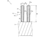
- FIG. 1 is a top view of the flexible printed wiring board of the first embodiment.
- FIG. 2 is a schematic end view of the AA line of FIG.
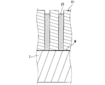
- FIG. 3 is a schematic end view for explaining a method of manufacturing the flexible printed wiring board of FIG.
- FIG. 4 is a schematic end view for explaining a method of manufacturing the flexible printed wiring board of FIG. 2.
- FIG. 5 is a schematic end view for explaining a method of manufacturing the flexible printed wiring board of FIG. 2.
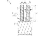
- FIG. 6 is a schematic end view showing the flexible printed wiring board of the third embodiment.
- the flexible printed wiring board according to one aspect of the present disclosure has excellent adhesiveness to an insulating film, and short circuits are suppressed.
- the method for manufacturing a flexible printed wiring board according to another aspect of the present disclosure can manufacture a flexible printed wiring board having excellent adhesiveness to an insulating film and suppressing short circuits.
- the flexible printed wiring board according to one aspect of the present disclosure is a flexible printed wiring board including a base film and a plurality of wirings arranged on the surface of the base film, and the wiring is along the longitudinal direction thereof. It has a tip surface and two sides along the longitudinal direction, the arithmetic mean roughness Ra of the side surfaces is 0.05 ⁇ m or more and 2.0 ⁇ m or less, and the average height of the wiring is 40 ⁇ m or more and 120 ⁇ m or less.
- the average spacing of the wiring is 1 ⁇ m or more and 30 ⁇ m or less.
- the arithmetic average roughness Ra on the side surface is within the above range, and the average height and the average spacing of the wiring are within the above range, so that a short circuit can be suppressed.
- the adhesiveness between the insulating film and the wiring can be increased. Therefore, the flexible printed wiring board has excellent adhesiveness to the insulating film, and short circuits are suppressed.
- the arithmetic average roughness Ra of the tip surface may be 0.05 ⁇ m or more and 2.0 ⁇ m or less.
- the adhesiveness between the insulating film and the wiring can be further increased. Therefore, the flexible printed wiring board is more excellent in adhesiveness to the insulating film.
- the average line width of the above wiring may be 5 ⁇ m or more and 30 ⁇ m or less.
- the average height of the wiring may be 40 ⁇ m or more and 60 ⁇ m or less.
- the adhesiveness between the insulating film and the wiring can be further increased and short circuit can be suppressed. Therefore, the superiority of the flexible printed wiring board is enhanced.
- the width of the wiring increases from the surface of the base film toward the tip surface in the cross section perpendicular to the longitudinal direction. According to this feature, the adhesiveness with the insulating film covering the wiring is excellent.
- the wiring includes a first conductive base layer laminated on the surface of the base film, a first plating layer laminated on the surface of the first conductive base layer opposite to the base film, and the first plating layer.
- the second plating layer includes a second plating layer laminated so as to cover both side surfaces of the conductive base layer and the surface and both side surfaces of the first plating layer opposite to the first conductive base layer.
- the tip surface and the side surface of the above correspond to the tip surface and the side surface of the wiring, respectively.
- the thickness of the second plating layer in the direction perpendicular to the side surface of the first plating layer increases from the contact surface between the surface of the base film and the second plating layer toward the tip surface. According to this feature, the adhesiveness with the insulating film covering the wiring is excellent.
- the wiring includes a first conductive base layer laminated on the surface of the base film and a third plating layer laminated on the surface of the first conductive base film opposite to the base film.
- the tip surface and the side surface of the third plating layer correspond to the tip surface and the side surface of the wiring, respectively.
- a method for manufacturing a flexible printed wiring board is a method for manufacturing a flexible printed wiring board including a base film and a plurality of wirings arranged on the surface of the base film.
- the tip surface along the longitudinal direction and the two side surfaces along the longitudinal direction, the arithmetic average roughness Ra of the side surfaces is 0.05 ⁇ m or more and 2.0 ⁇ m or less, and the average height of the wiring is
- a base film having a diameter of 40 ⁇ m or more and 120 ⁇ m or less, an average spacing of the wirings of 1 ⁇ m or more and 30 ⁇ m or less, and a conductive base layer laminated on the surface is prepared, and the conductivity is used in the first plating solution using a resist pattern.
- a second plating step of forming a second plating layer by electroplating the first plating layer in a second plating solution after the step of removing the laminated region and the step of removing the laminated region is provided.
- the second plating solution contains polyethylene glycol having a number average molecular weight of 2500 or more and 8000 or less, and in the second plating step, the arithmetic average roughness Ra of the side surface is 0.05 ⁇ m or more and 2.0 ⁇ m or less. Adjust the current density of the electroplating.
- the above-mentioned flexible printed wiring board can be manufactured. That is, it is possible to manufacture a flexible printed wiring board having excellent adhesiveness between the wiring and the insulating film covering the wiring and suppressing short circuits.
- the current density may be adjusted in two steps.
- the “height direction” as used herein means the direction perpendicular to the surface of the base film on which the wiring is formed.
- the “average height of wiring” means an average value of heights measured at any ten points of one wiring.
- “Height” means the distance from the base film to the top edge of the wiring in a direction perpendicular to the plane of the base film. "Height" corresponds to "thickness”.
- the "spacing" of wiring means the distance between adjacent surfaces of two opposing wirings.
- the "average distance” means a value obtained by exposing a wiring cross section perpendicular to the longitudinal direction with a cross-section processing device such as a microtome and averaging the distances between adjacent surfaces by observing a cross-section at any ten points.
- the "line width" of a wire means the dimension of the width of the wire in the direction perpendicular to the longitudinal direction.
- the “average line width” means a value obtained by exposing the wiring cross section with a cross-section processing device such as a microtome and averaging each maximum width by observing the cross-sections of any ten points.
- the land part having vias (through holes, blind vias, filled vias) for connecting each wiring, the land part for connecting with the mounting parts, the land part for connecting with other printed circuit boards and connectors, etc.
- the land portion shall be excluded from the "height", "line width” and "interval" specified above.
- Arithmetic mean roughness Ra of the side surface means the calculated average roughness Ra of each side surface in each wiring.
- the "arithmetic mean roughness Ra of the tip surface” means the calculated average roughness Ra of the entire tip surface in each wiring.
- the term “arithmetic mean roughness Ra” as used herein means an average value of arithmetic mean roughness Ra measured at any five points on the side surface or the tip surface of the wiring.
- the arithmetic mean roughness Ra at any of the five locations is the average line of the extracted portion by extracting only the reference length (L) from position 0 to position L in the direction of the average line from the roughness curve at each location.
- the "surface” refers to the surface of the base film on the side where the wiring is laminated in the height direction
- the front and back of the present embodiment are the front and back of the flexible printed wiring board in use. Does not determine.
- FIG. 1 is a top view of the flexible printed wiring board 10 of the present embodiment.
- FIG. 2 is a schematic cross-sectional view of the AA line.
- the flexible printed wiring board 10 of the present embodiment has an insulating base film 3 and a plurality of wirings 13 arranged (laminated) on one surface of the base film 3. It mainly includes a wiring layer 11 having the wiring layer 11.
- the flexible printed wiring board 10 may further include an insulating film (cover film) on the surface of the base film 3 or the wiring layer 11. Examples of the insulating film include a conventionally known resin film, and the insulating film is adhered to the base film 3 or the wiring layer 11 by, for example, an adhesive.
- the base film 3 is a layer made of a synthetic resin having an insulating property.
- the base film 3 has flexibility.
- the base film 3 is also a base material for forming the wiring layer 11.
- the material for forming the base film 3 is not particularly limited as long as it has insulating properties and flexibility, but a synthetic resin film having a low dielectric constant formed in a sheet shape can be adopted.
- the main component of this synthetic resin film include polyimide, polyethylene terephthalate, liquid crystal polymer, fluororesin and the like.
- the "main component” is a component having the highest content, and means, for example, a component that occupies 50% by mass or more in the forming material.
- the base film 3 may contain a resin other than the exemplified resin such as polyimide, an antistatic agent, and the like.
- the lower limit of the average thickness of the base film 3 is not particularly limited, but may be 3 ⁇ m, 5 ⁇ m, or 10 ⁇ m.
- the upper limit of the average thickness of the base film 3 is not particularly limited, but may be 200 ⁇ m, 150 ⁇ m, or 100 ⁇ m. If the average thickness of the base film 3 is less than 3 ⁇ m, the dielectric strength and mechanical strength of the base film 3 may be insufficient. On the other hand, when the average thickness of the base film 3 exceeds 200 ⁇ m, the flexible printed wiring board 10 may become unnecessarily thick.
- the "average thickness” means the average value of the thickness measured at any ten points. In the following, the "average thickness" of other members and the like is also measured in the same manner.
- the wiring layer 11 is arranged (laminated) directly on the surface of the base film 3 or via another layer.
- Examples of the wiring 13 included in the wiring layer 11 include a signal line for transmitting a signal, a current line for transmitting a current for power supply, a current line for transmitting a current for generating a magnetic field, and the like.
- the wiring 13 is arranged (laminated) on the surface of the first conductive base layer 23 opposite to that of the base film 3 and the first conductive base layer 23 arranged (laminated) on the surface of the base film 3.
- the plating layer 25 is arranged (laminated) so as to cover both side surfaces of the first conductive base layer 23 and the surface and both side surfaces of the first plating layer 25 on the side opposite to the first conductive base layer 23. 2 Formed by the plating layer 27.
- the cross section of the wiring 13 has a shape such that the width increases from the connection portion of the wiring 13 with the base film 3 toward the tip of the wiring 13.
- the cross section has a shape that tapers toward the base film 3. That is, the cross section has an inverted trapezoidal shape. Since the cross section has an inverted trapezoidal shape as described above, the adhesiveness between both side surfaces of the wiring 13 and the insulating film can be further increased. Therefore, the flexible printed wiring board 10 is more excellent in adhesiveness to the insulating film.
- the thickness of the second plating layer 27 in the direction perpendicular to the side surface of the first plating layer 25 is the tip surface of the wiring 13 from the contact surface between the surface of the base film and the second plating layer 27. It gets bigger towards.
- the lower limit of the average line width L1 of the wiring 13 may be 5 ⁇ m, 7.5 ⁇ m, or 10 ⁇ m.
- the upper limit of the average line width L1 of the wiring 13 may be 30 ⁇ m, 25 ⁇ m, or 20 ⁇ m. If the average line width L1 of the wiring 13 is less than 5 ⁇ m, it may be difficult to manufacture the wiring 13. On the other hand, when the average line width L1 of the wiring 13 exceeds 30 ⁇ m, a sufficient wiring density may not be obtained.
- the "average line width" is determined by exposing the cross section of the flexible printed wiring board 10 with a cross section processing device such as a microtome and measuring the length of the widest portion of each wiring 13 with a measurable microscope or the like. It is a value calculated as an average value of points.
- the lower limit of the average spacing S1 of the plurality of wirings 13 arranged adjacent to each other is 1 ⁇ m, and may be further 2 ⁇ m.
- the upper limit of the average spacing S1 of the wiring 13 is 30 ⁇ m, and may be 20 ⁇ m or 10 ⁇ m. If the average spacing S1 of the wiring 13 is less than 1 ⁇ m, a short circuit may occur. On the other hand, if the average spacing S1 of the wiring 13 exceeds 30 ⁇ m, a sufficient wiring density may not be obtained.
- the "average spacing" is determined by exposing the cross section of the flexible printed wiring board 10 with a cross-section processing device such as a microtome, measuring the length of the smallest spacing in the gap between the wiring 13 with a microscope or the like capable of measuring them. It is a value calculated as an average value of.
- the lower limit of the average height (thickness) H1 of the wiring 13 is 40 ⁇ m, and may be further 50 ⁇ m.
- the upper limit of the average height H1 of the wiring 13 is 120 ⁇ m, and may be 100 ⁇ m, 70 ⁇ m, or 60 ⁇ m. If the average height H1 is less than 40 ⁇ m, the mechanical strength may be insufficient. On the other hand, when the average height H1 exceeds 120 ⁇ m, it may be difficult to form the wiring 13 by the method for manufacturing the flexible printed wiring board 10 described later.
- the “average height” is determined by exposing the cross section of the flexible printed wiring board 10 with a cross-section processing device such as a microtome, and measuring the height (corresponding to the thickness) by observing the cross section of any ten points in the wiring 13. It is obtained by calculating the average value of the measurement results. In the following, the "average height" of other members and the like is also measured in the same manner.
- the first conductive base layer 23 is formed by a part of the conductive base layer M (see, for example, FIG. 3) described later.
- Examples of the material for forming the first conductive base layer 23 include copper (Cu), silver (Ag), gold (Au), nickel (Ni), titanium (Ti), chromium (Cr), and alloys thereof. Be done. Regarding these forming materials, in terms of suppressing thermal deterioration of the adhesion of the wiring layer 11 to the base film 3, on the side where the first conductive base layer 23 is in contact with the base film 3 (for example, polyimide), nickel, chromium, etc. are used.
- a layer (first layer) containing at least one selected from the group consisting of titanium and silver may be included.
- the first conductive base layer 23 may include a layer (first layer) containing at least one selected from nickel and chromium, which are easy to remove and easily maintain insulating properties. Further, the first conductive base layer 23 may include a layer containing copper as a main component (second layer) on the upper side (the side opposite to the base film 3) of the first layer. By arranging the layer containing copper as a main component, it is possible to shorten the work time when forming the wiring layer 11 by electroplating.
- the lower limit of the average thickness of the first layer may be 1 nm or 2 nm.
- the upper limit of the average thickness of the first layer may be 15 nm or 8 nm. If the average thickness is less than 1 nm, it may be difficult to suppress thermal deterioration of the adhesion of the wiring layer 11 to the base film 3. On the other hand, when the average thickness exceeds 15 nm, it becomes difficult to easily remove the first layer, and there is a possibility that the insulating property of the wiring layer 11 cannot be sufficiently maintained.
- the first layer may be formed by a sputtering method, an electroplating method, an electroless plating method, or the like.
- the lower limit of the average thickness of the second layer may be 0.1 ⁇ m or 0.2 ⁇ m.
- the upper limit of the average thickness of the second layer may be 2 ⁇ m or 1 ⁇ m. If the average thickness is less than 0.1 ⁇ m, the time for forming the wiring layer 11 by electroplating may become excessively long. On the other hand, when the average thickness exceeds 2 ⁇ m, it becomes difficult to easily remove the second layer, and there is a possibility that the insulating property of the wiring layer 11 cannot be sufficiently maintained.
- the second layer may be formed by a sputtering method, an electroplating method, an electroless plating method, or the like, or may be formed by combining these.
- the electroless copper plating layer may be arranged on the uppermost surface side of the first conductive base layer 23, and this sputtering method is used when the inner layer is formed by the sputtering method. It is possible to cover defects and the like that may occur due to.
- the first metal material for forming the first plating layer 25 for example, copper, nickel, gold, silver, platinum and the like can be used, among which copper, which is relatively inexpensive and has excellent conductivity, and relatively inexpensive and corrosion resistant. Nickel, which is excellent in quality, is preferably used.
- the first plating layer 25 is formed by using a resist pattern as described later. That is, the first plating layer 25 is formed while its two side surfaces along the longitudinal direction are in contact with the resist pattern.
- the second forming material for forming the second plating layer 27 for example, copper, nickel, gold, silver, platinum or the like can be used as in the case of the first metal material, and among them, it is relatively inexpensive and has excellent conductivity. Copper and nickel, which is relatively inexpensive and has excellent corrosion resistance, are preferably used.
- the second plating layer 27 is formed without using a resist pattern, as will be described later.
- the tip surface 27a along the longitudinal direction in the second plating layer 27 corresponds to the tip surface along the longitudinal direction in the wiring 13, and the two side surfaces 27b along the longitudinal direction in the second plating layer 27.
- And 27c (the left and right sides of FIG. 2) correspond to the two sides of the wiring 13 along the longitudinal direction.
- the arithmetic average roughness Ra of these two sides 27b and 27c is 0.05 or more and 2.0 or less.
- the lower limit of the arithmetic average roughness Ra of each side surface 27b and 27c is 0.05, and may be further 0.1.
- the upper limit of the arithmetic mean roughness Ra of each of the side surfaces 27b and 27c is 2.0, and may be 1.0 or 0.7, respectively. If Ra is less than 0.05, the adhesiveness with the insulating film may be inferior. On the other hand, when Ra exceeds 2.0, the high frequency characteristics may deteriorate. In addition, if Ra exceeds 2.0, a short circuit may occur between the adjacent wirings 13. Ra is measured by the method described in Examples described later.
- the arithmetic average roughness Ra of the tip surface 27a of the wiring 13 is not particularly limited.
- the lower limit of the arithmetic average roughness Ra of the tip surface 27a may be 0.05 or 0.1.
- the upper limit of Ra of the tip surface 27a may be 2.0, 1.0, or 0.7. If Ra is less than 0.05, the adhesiveness with the insulating film may not be sufficiently enhanced. On the other hand, when Ra exceeds 2.0, the high frequency characteristics may deteriorate.
- the arithmetic mean roughness Ra of the tip surface 27a is measured in the same manner as the method for measuring Ra on the side surface described in Examples described later, without changing the measurement target from the side surface to the tip surface and cutting the base film in particular. To.
- the arithmetic average roughness Ra of the two side surfaces 27b, 27c, and the tip surface 27a can be adjusted by adjusting the additive in the second plating solution and the current density, as will be described later.
- the average height H1 and the average interval S1 of the wiring 13 are in the above range, and the arithmetic mean roughness Ra of the side surfaces 27b and 27c is within the above range, so that a short circuit can be suppressed. ..
- the adhesiveness between the insulating film and the wiring 13 can be increased. Therefore, the flexible printed wiring board 10 has excellent adhesiveness to the insulating film, and short circuits are suppressed.
- the method for manufacturing the flexible printed wiring board 10 is to prepare a base film 3 on which the conductive base layer M is laminated on the surface, use the resist pattern R1, and use the resist pattern R1 in the first plating solution to prepare the conductive base layer 3 on the base film 3.
- the second plating layer 27 is formed by electroplating the first plating layer 25 in the second plating solution.
- a second plating step is provided.
- the second plating solution contains polyethylene glycol having a number average molecular weight of 2500 or more and 8000 or less.
- the current density of electroplating is such that the arithmetic mean roughness Ra of the side surface of the wiring 13 (here, the two side surfaces 27b and 27c of the second plating layer 27) is 0.05 or more and 2.0 or less. To adjust.
- the conductive base layer M is laminated on the surface of the base film 3. As the conductive base layer M, one laminated in advance on the entire surface of the base film 3 is used. A part of the conductive base layer M becomes the first conductive base layer 23.
- Examples of the material for forming the conductive base layer M include copper (Cu), silver (Ag), gold (Au), nickel (Ni), titanium (Ti), chromium (Cr), and alloys thereof. Regarding these forming materials, in terms of suppressing thermal deterioration of the adhesion of the wiring layer 11 to the base film 3, on the side where the conductive base layer M is in contact with the base film 3 (for example, polyimide), nickel, chromium, titanium and the like are used. A layer (first layer) containing at least one selected from the group consisting of silver may be included. Further, the conductive base layer M may include a layer (first layer) containing at least one selected from nickel and chromium, which are easy to remove and easily maintain insulating properties.
- the conductive base layer M may include a layer containing copper as a main component (second layer) on the upper side (the side opposite to the base film 3) of the first layer.
- second layer a layer containing copper as a main component
- the lower limit of the average thickness of the first layer may be 1 nm or 2 nm.
- the upper limit of the average thickness of the first layer may be 15 nm or 8 nm. If the average thickness is less than 1 nm, it may be difficult to suppress thermal deterioration of the adhesion of the wiring layer 11 to the base film 3. On the other hand, when the average thickness exceeds 15 nm, it becomes difficult to easily remove the first layer, and there is a possibility that the insulating property of the wiring layer 11 cannot be sufficiently maintained.
- the first layer may be formed by a sputtering method, an electroplating method, an electroless plating method, or the like.
- the lower limit of the average thickness of the second layer may be 0.1 ⁇ m or 0.2 ⁇ m.
- the upper limit of the average thickness of the second layer may be 2 ⁇ m or 1 ⁇ m. If the average thickness is less than 0.1 ⁇ m, the time for forming the wiring layer 11 by electroplating may become excessively long. On the other hand, when the average thickness exceeds 2 ⁇ m, it becomes difficult to easily remove the second layer, and there is a possibility that the insulating property of the wiring layer 11 cannot be sufficiently maintained.
- the second layer may be formed by a sputtering method, an electroplating method, an electroless plating method, or the like, or may be formed by combining these.
- the electroless copper plating layer may be arranged on the uppermost surface side of the conductive base layer M, whereby defects and the like that may occur by this sputtering method when the inner layer is formed by the sputtering method. Can be covered.
- This step includes a step of laminating a resist film on the surface of the conductive base layer M, a step of forming an inverted resist pattern of the first plating layer 25 by exposure and development of the resist film, and this resist. A step of forming the first plating layer 25 by electroplating on the conductive base layer M at the opening of the pattern is provided.
- Step of laminating the photoresist film In the step of laminating the photoresist film, the photoresist film (not shown) is laminated on the surface of the conductive base layer M.
- the photoresist film is a negative resist composition in which the bond of the polymer is strengthened by exposure to light and the solubility in the developer is lowered, or the bond of the polymer is weakened by exposure to light and the solubility in the developer is reduced. It is formed by an increasing positive resist composition.
- the photoresist film may be formed on the conductive base layer M by coating and drying a liquid resist composition, or a dry film photoresist having no fluidity at room temperature may be laminated by thermocompression bonding. ..
- a dry film photoresist as the photoresist film, the thickness of the photoresist film can be made uniform and small, so that the resist pattern can be easily made finer.
- the lower limit of the average height (thickness) of the photoresist film may be 45 ⁇ m or 50 ⁇ m.
- the upper limit of the average height of the photoresist film may be 170 ⁇ m or 150 ⁇ m. If the average height of the photoresist film is less than 45 ⁇ m, the dry film resist may not be easy to handle. On the other hand, if the average height of the photoresist film exceeds 170 ⁇ m, the accuracy of the shape of the resist pattern may decrease.
- Step of forming a resist pattern In the step of forming the resist pattern, first, the photoresist film is selectively exposed using, for example, a photomask to form a portion that dissolves in the developing solution and a portion that does not dissolve in the photoresist film.
- a resist pattern R1 having an opening portion corresponding to the first plating layer 25 to be formed as shown in FIG. 3 is formed. obtain.
- the resist pattern R1 has a plurality of openings defining the first plating layer 25.
- the lower limit of the average width of this opening may be 5 ⁇ m, 10 ⁇ m, or 15 ⁇ m.
- the upper limit of the average width of the opening may be 50 ⁇ m, 40 ⁇ m, or 30 ⁇ m. If the average width of the opening is smaller than 5 ⁇ m, the width of the opening may vary widely, and the height (secondary plating amount) of the second plating layer 27 becomes too large, resulting in dimensional variation and flexibility. The manufacturing cost of the printed wiring board may increase. On the contrary, if the average width of the openings exceeds 50 ⁇ m, the resist pattern R1 may be easily peeled off, and the wiring density may not meet the requirements.
- the average width of the opening corresponding to the first plating layer 25 of the resist pattern R1 is the same as the average width of the first plating layer 25 before etching in the first removal step described later.
- Step of forming the first plating layer In the step of forming the first plating layer, a first plating solution is used to laminate a metal on the conductive base layer M exposed in the opening of the resist pattern R1 by electroplating, and as shown in FIG. 4, the first plating layer is formed. 1 The plating layer 25 is formed.
- a laminate of the base film 3, the conductive base layer M, and the resist pattern R1 and an electrode facing the laminate are arranged in the first plating solution.
- the metal in the first plating solution is deposited on the surface of the conductive base layer M.
- copper, nickel, gold, silver, platinum or the like can be used as the metal to be laminated by electroplating, that is, the first metal material for forming the first plating layer 25, and among them, relatively Copper, which is inexpensive and has excellent conductivity, and nickel, which is relatively inexpensive and has excellent corrosion resistance, are preferably used.
- Examples of the first plating solution include those containing a first metal material and a first additive.
- a first additive in addition to polyethylene glycol described later, copper sulfate pentahydrate, sulfuric acid, chloride ion (chloride ion), 3,3'-dithiobis (1-propanesulfonic acid) disodium (SPS), etc. Can be mentioned.
- SPS 3,3'-dithiobis (1-propanesulfonic acid) disodium
- the first plating solution the same one as the second plating solution described later can be used.
- the lower limit of the average height of the first plating layer 25 before etching formed in the step of forming the first plating layer may be 20 ⁇ m, 25 ⁇ m, or 30 ⁇ m.
- the upper limit of the average height of the first plating layer 25 before etching may be 125 ⁇ m, 120 ⁇ m, or 118 ⁇ m. If the average height of the first plating layer 25 before etching is smaller than 20 ⁇ m, the height (secondary plating amount) of the second plating layer 27 becomes too large, resulting in dimensional variation and manufacturing cost of the flexible printed wiring board. May increase. On the contrary, if the average height of the first plating layer 25 before etching exceeds 125 ⁇ m, the resist pattern R1 may be difficult to peel off, or the flexible printed wiring board 10 may become unnecessarily thick.
- the resist pattern R1 is removed by peeling the resist pattern R1 from the conductive base layer M.
- the resist pattern R1 is expanded by the stripping liquid by immersing the laminate having the resist pattern R1, the first plating layer 25, the conductive base layer M, and the base film 3 in the stripping liquid.
- a repulsive force is generated between the resist pattern R1 and the conductive base layer M, and the resist pattern R1 is peeled off from the conductive base layer M.
- a known release liquid can be used.
- the first plating layer 25 acts as a mask and removes the conductive base layer M exposed after the resist pattern R1 is peeled off by etching. As a result, the plurality of plating layers 25 are electrically separated. An etching solution that erodes the metal forming the conductive base layer M is used for this etching.
- the etching amount may be any amount as long as the conductive base layer M is completely removed, but in the method for manufacturing the flexible printed wiring board 10, the average etching amount of the first plating layer 25 is 0.5 ⁇ m or more and less than 3.0 ⁇ m. May be. Further, the average etching amount may be 2.0 ⁇ m or less.
- the "average etching amount of the first plating layer” is the difference between the area of the first plating layer before etching and the area of the first plating layer after etching in the cross section perpendicular to the longitudinal direction of the wiring before etching. It is a value obtained by averaging the thickness obtained by dividing by the length of the outer surface (excluding the laminated surface with the base film) of the first plating layer in the longitudinal direction of the wiring.
- the second plating solution is used to coat the surface of the first plating layer 25 with the second plating layer 27 by electroplating to form the wiring 13.
- This electroplating can be performed, for example, by using a known electroplating method and adjusting the current density as described later.
- the flexible printed wiring board 10 of FIG. 2 as described above can be obtained.
- the so-called semi-additive method is preferably used as described above.
- copper, nickel, gold, silver, platinum or the like can be used as the metal to be laminated by electroplating, that is, the second metal material for forming the second plating layer 27, and among them, relatively Copper, which is inexpensive and has excellent conductivity, and nickel, which is relatively inexpensive and has excellent corrosion resistance, are preferably used.
- the second plating solution used in this electroplating contains polyethylene glycol (PEG) having a number average molecular weight of 2500 or more and 8000 or less.
- PEG polyethylene glycol
- Examples of the second plating solution include those containing a second metal material and polyethylene glycol as a second additive.
- the second additive other than polyethylene glycol include copper sulfate pentahydrate, sulfuric acid, chlorine ion (chloride ion), and 3,3'-dithiobis (1-propanesulfonic acid), as in the case of the first additive described above. 2 Sodium (SPS) and the like can be mentioned.
- the lower limit of the number average molecular weight Mn of polyethylene glycol is 2500, and may be 2700 or 3000.
- the upper limit of the number average molecular weight Mn is 8000, and may be further 7000 or 5000.
- the number average molecular weight Mn is less than 2500, it may be difficult to set the arithmetic average roughness Ra of the two side surfaces 27b and 27c of the second plating layer 27 and the tip surface 27a within the above range.
- the number average molecular weight Mn exceeds 8000, it may be difficult to set the arithmetic average roughness Ra of the two side surfaces 27b, 27c and the tip surface 27a of the second plating layer 27 within the above range.
- the lower limit of the weight average molecular weight Mw of polyethylene glycol may be 10000 or 10100.
- the upper limit of the weight average molecular weight Mw may be 20000, 18000, 16000, or 15000.
- the weight average molecular weight Mw is less than 10000, it may be difficult to set the arithmetic average roughness Ra of the two side surfaces 27b, 27c and the tip surface 27a of the second plating layer 27 within the above range.
- the weight average molecular weight Mw exceeds 20000, it may be difficult to set the arithmetic average roughness Ra of the two side surfaces 27b, 27c and the tip surface 27a of the second plating layer 27 within the above range.
- the lower limit of the z average molecular weight Mz of polyethylene glycol may be 15,000 or 16,000.
- the upper limit of the z average molecular weight Mz may be 25,000, 22,000, or 20,000.
- the z average molecular weight Mz is less than 15,000, it may be difficult to set the arithmetic average roughness Ra of the two side surfaces 27b, 27c and the tip surface 27a of the second plating layer 27 within the above range.
- the z average molecular weight Mz exceeds 25,000, it may be difficult to set the arithmetic average roughness Ra of the two side surfaces 27b, 27c and the tip surface 27a of the second plating layer 27 within the above range.
- the current density in the second plating step is not particularly limited and may be appropriately set.
- the lower limit of the current density may be 0.3 A / m 2 in total, 0.5 A / m 2 , or 1 A / m 2 .
- the upper limit of the current density may be 5 A / m 2 in total, 4 A / m 2 , or 3 A / m 2 . If the current density is less than 0.3 A / m 2 , it may be difficult to set the arithmetic average roughness Ra of the two side surfaces 27b, 27c and the tip surface 27a of the second plating layer 27 within the above range. There is.
- the current density may be adjusted in one step or two steps. As described above, by adjusting the current density in two steps in the second plating step, it becomes easy to adjust the arithmetic mean roughness Ra within the above range. When the current density is adjusted in one step, the lower and upper limits of the current density may be in the above range.
- the current density in the second step may be higher than the current density in the first step.
- the lower limit of the current density in the first stage may be 0.1 A / m 2 or 0.3 A / m 2 .
- the upper limit of the current density in the first stage may be 1.5 A / m 2 or 1.0 A / m 2 .
- the lower limit of the current density in the second stage may be 0.2 A / m 2 or 1.0 A / m 2 .
- the upper limit of the current density in the second stage may be 5 A / m 2 or 3 A / m 2 .
- the method for manufacturing the flexible printed wiring board 10 it is possible to manufacture the flexible printed wiring board 10 having excellent adhesiveness to the insulating film and suppressing short circuits. According to the manufacturing method of the flexible printed wiring board 10, even if the wiring pattern is relatively dense (the average height of the wiring is 40 ⁇ m or more and 120 ⁇ m or less, and the average spacing of the wiring is 1 ⁇ m or more and 30 ⁇ m or less), the side surface of the wiring is predetermined. It is possible to adjust the surface roughness.
- the flexible printed wiring board 30 of the present embodiment has a wiring layer 31 having an insulating base film 3 and a plurality of wirings 33 arranged (laminated) on one surface of the base film 3. Mainly prepared for. Similar to the first embodiment described above, the flexible printed wiring board 30 may further include an insulating film (cover film) on the surface of the base film 3 or the wiring layer 31.
- the wiring 33 has a second conductive base layer 43 and one third plating layer 45 arranged on the second conductive base layer 43.
- the wiring layer 31 is arranged (laminated) directly on the surface of the base film 3 or via another layer.
- the wiring 33 included in the wiring layer 31 includes, for example, a signal line for transmitting a signal, a current line for transmitting a current for power supply, and a current for transmitting a current for generating a magnetic field, as in the first embodiment described above. Lines and the like can be mentioned.
- the wiring 33 is arranged (laminated) on the surface of the second conductive base layer 43 opposite to the base film 3 of the second conductive base layer 43 arranged (laminated) on the surface of the base film 3. 3 Formed by the plating layer 45.
- the average line width L2, the average interval S2, and the average height H2 of the wiring 33 can be set in the same manner as the wiring 13 of the first embodiment.
- the same material as that of the first conductive base layer 23 of the first embodiment can be used.
- the third metal material for forming the third plating layer 45 is the same as the first metal material and the second metal material for forming the first plating layer 25 and the second plating layer 27 of the first embodiment. Can be used.
- the left and right side surfaces of 6) 45b and 45c correspond to the two side surfaces of the wiring 33 along the longitudinal direction.
- the tip surface 45a along the longitudinal direction in the third plating layer 45 corresponds to the tip surface along the longitudinal direction in the wiring 33.
- the arithmetic average roughness Ra of the two sides of the wiring 33 is 0.05 or more and 2.0 or less, as in the first embodiment described above.
- the lower limit of the arithmetic mean roughness Ra on the side surface of the wiring 33 is 0.05 as in the first embodiment described above, and may be further 0.1.
- the upper limit of Ra on the side surface is 2.0, and may be 1.0 or 0.7.
- the lower limit of the arithmetic average roughness Ra of the tip surface of the wiring 33 may be 0.05 as in the first embodiment described above, or 1.0. May be.
- the upper limit of Ra on the tip surface may be 2.0, 1.0, or 0.7, as in the first embodiment described above.
- the corresponding portions of the two side surfaces of the wiring 33 and the arithmetic mean roughness Ra of the tip surface can be adjusted by adjusting the etching conditions as described later.
- the flexible printed wiring board 30 is manufactured by using a resist pattern R2 (not shown) on the conductive base layer M of the base film 3 in which the conductive base layer M is laminated on one surface in the third plating solution.
- a third plating step of forming the third plating layer 45 by electroplating a second removing step of removing the non-stacked region of the third plating layer 45 in the resist pattern R2 and the conductive base layer M, and a first step.
- a surface roughness adjusting step of adjusting the arithmetic average roughness Ra of the surface of the third plating layer 45 is provided.
- the surface roughness of the third plating layer 45 is adjusted so that Ra on the side surface of the third plating layer 45 is 0.05 or more and 2.0 or less.
- the surface roughness of the third plating layer 45 and the second conductive base layer 43 is adjusted so that Ra on each side surface of the wiring 33 is 0.05 or more and 2.0 or less.
- the surface roughness of the third plating layer 45 is adjusted so that Ra of the tip surface of the wiring 33 (that is, the tip surface 45a of the third plating layer 45) is 0.05 or more and 2.0 or less.
- conductive base layer M As the conductive base layer M, the same one as in the second embodiment described above is used. A part of the conductive base layer M becomes the second conductive base layer 43.
- This step is the same as the first plating step of the second embodiment.
- a laminated body in which the third plating layer 45 is laminated on the opening of the resist pattern R2 (not shown) in the conductive base layer M can be obtained.
- both side surfaces 43b and 43c of the second conductive base layer 43 and both side surfaces 45b and 45c and the tip surface 45a of the third plating layer 45 are etched to adjust their surface roughness.
- An etching solution such as hydrogen peroxide is used for this etching.
- the surface roughness adjusting step may be performed at the same time as the etching of the conductive base layer M in the second removing step.
- the average height H2 and the average interval S2 of the wiring 33 are in the above range, and the arithmetic average roughness Ra of the side surface is within the above range, so that a short circuit can be suppressed.
- the adhesiveness between the insulating film and the wiring 33 can be increased. Therefore, the flexible printed wiring board 30 has excellent adhesiveness to the insulating film, and short circuits are suppressed.
- the flexible printed wiring board 10 is used for both of the single base films.
- the wiring layer may be laminated on the surface.
- the flexible printed wiring board 10 may be a multilayer printed wiring board having a plurality of base films, each base film having a plurality of wiring layers on one surface or both surfaces. In this case, the wiring layers on both sides may be conducted via the land portion.
- each wiring layer 11 and 31 has the respective wirings 13 and 33 has been described, but an embodiment in which each wiring layer 11 and 31 has wirings other than these wirings 13 and 33 can also be adopted.
- the type of PEG was changed as shown in Table 1 using a plating solution having the following composition.
- Each molecular weight of PEG shown in Table 1 was measured by the following method. Copper sulfate pentahydrate: 75 g / L Sulfuric acid: 190 g / L Hydrochloric acid (source of chloride ion): 55 mg / L PEG: 0.02 mmol / L 3,3'-Dithiobis (1-propanesulfonic acid) disodium (SPS): 0.5 mmol / L Janus Green B (JGB): 0.05 mmol
- Detector Differential refractive index detector RI (RI-201 manufactured by Showa Denko KK, Sensitivity: 32)
- Solvent 0.1 M aqueous sodium nitrate flow rate: 0.7 mL / min
- Column temperature 23 ° C
- Injection volume 0.2 mL
- Standard sample Monodisperse polyethylene oxide (PEO) and polyethylene glycol (PEG) manufactured by Tosoh, Agilent and Sigma-Aldrich.
- PEO Polyethylene oxide
- PEG polyethylene glycol
- the number average molecular weight Mn, the weight average molecular weight Mw, and the z average molecular weight Mz were calculated as shown in the following definition formulas.
- Mi is the molecular weight of each elution position of the GPC curve obtained via the molecular weight calibration curve
- Ni is the number of molecules.
- Mz ⁇ (Ni ⁇ Mi 3 ) / ⁇ (Ni ⁇ Mi 2 )
- Conductivity is obtained by using each plating solution and electroplating the conductive base layer of the film under each plating condition by using a resist pattern in the same manner as in the first plating step of the second embodiment described above.
- the first plating layer was formed on the base layer.
- the resist pattern was peeled off, and the conductive base layer was etched using the first plating layer as a mask.
- the second plating layer was formed by performing electroplating in the same manner as in the second plating step of the second embodiment described above, using the same conditions as those at the time of forming the first plating layer.
- the plating solution and plating conditions used in the formation of each first plating layer were used as they were in the formation of each second plating layer.
- the average spacing and average height of the wiring after forming the second plating layer are as shown in Table 1.
- the short circuit rate (%) was measured by measuring the resistance of each wiring board using the 4-terminal method. The results are shown in Table 1.
- the case is less than 2 "3"
- the case is less than 10 mm 2 or more 20 mm 2 "4", and is less than 10 mm 2 (including the case of 0 mm 2) was evaluated as "5".
- the results are shown in Table 1.
- Comparative Example 1 in which the average spacing of the wiring is 30 ⁇ m or less, it was shown that a large short circuit occurs when the calculated average roughness Ra exceeds 2.0.
- Comparative Example 2 in which the average spacing of the wiring is 30 ⁇ m or less, it was shown that when the arithmetic average roughness Ra is less than 0.05 ⁇ mm, the short circuit is suppressed but the adhesion is inferior.
- the arithmetic average roughness Ra of the side surface of the wiring is 0.05 ⁇ m or more and 2.0 ⁇ m or less. It was shown that short circuit was suppressed and the adhesion to the insulating film was excellent.
Landscapes
- Engineering & Computer Science (AREA)
- Chemical & Material Sciences (AREA)
- Metallurgy (AREA)
- Chemical Kinetics & Catalysis (AREA)
- Electrochemistry (AREA)
- Materials Engineering (AREA)
- Organic Chemistry (AREA)
- Microelectronics & Electronic Packaging (AREA)
- Automation & Control Theory (AREA)
- Manufacturing & Machinery (AREA)
- Manufacturing Of Printed Wiring (AREA)
- Electroplating Methods And Accessories (AREA)
- Structure Of Printed Boards (AREA)
Priority Applications (3)
| Application Number | Priority Date | Filing Date | Title |
|---|---|---|---|
| JP2022535005A JP7304492B2 (ja) | 2020-07-08 | 2021-06-23 | フレキシブルプリント配線板及びその製造方法 |
| CN202180012005.4A CN115024025A (zh) | 2020-07-08 | 2021-06-23 | 柔性印刷布线板及其制造方法 |
| US17/791,931 US12267952B2 (en) | 2020-07-08 | 2021-06-23 | Flexible printed wiring board and method of manufacturing the same |
Applications Claiming Priority (2)
| Application Number | Priority Date | Filing Date | Title |
|---|---|---|---|
| JP2020117888 | 2020-07-08 | ||
| JP2020-117888 | 2020-07-08 |
Publications (1)
| Publication Number | Publication Date |
|---|---|
| WO2022009675A1 true WO2022009675A1 (ja) | 2022-01-13 |
Family
ID=79552950
Family Applications (1)
| Application Number | Title | Priority Date | Filing Date |
|---|---|---|---|
| PCT/JP2021/023701 Ceased WO2022009675A1 (ja) | 2020-07-08 | 2021-06-23 | フレキシブルプリント配線板及びその製造方法 |
Country Status (4)
| Country | Link |
|---|---|
| US (1) | US12267952B2 (https=) |
| JP (1) | JP7304492B2 (https=) |
| CN (1) | CN115024025A (https=) |
| WO (1) | WO2022009675A1 (https=) |
Cited By (2)
| Publication number | Priority date | Publication date | Assignee | Title |
|---|---|---|---|---|
| JP7680647B1 (ja) * | 2024-10-22 | 2025-05-20 | 住友電気工業株式会社 | プリント配線板 |
| JP7713613B1 (ja) * | 2024-10-22 | 2025-07-25 | 住友電気工業株式会社 | プリント配線板及びプリント配線板の製造方法 |
Families Citing this family (2)
| Publication number | Priority date | Publication date | Assignee | Title |
|---|---|---|---|---|
| US12016130B2 (en) * | 2021-05-26 | 2024-06-18 | Samsung Electro-Mechanics Co., Ltd. | Method of manufacturing printed circuit board |
| CN119450910A (zh) * | 2023-07-28 | 2025-02-14 | 鹏鼎控股(深圳)股份有限公司 | 高频传输电路板及其制作方法 |
Citations (4)
| Publication number | Priority date | Publication date | Assignee | Title |
|---|---|---|---|---|
| JP2014192523A (ja) * | 2013-03-26 | 2014-10-06 | Samsung Electro-Mechanics Co Ltd | パワーインダクタおよびその製造方法 |
| JP2016219559A (ja) * | 2015-05-19 | 2016-12-22 | 新光電気工業株式会社 | 配線基板及びその製造方法と電子部品装置 |
| JP2019186518A (ja) * | 2018-04-06 | 2019-10-24 | サムソン エレクトロ−メカニックス カンパニーリミテッド. | コイル部品及びその製造方法 |
| JP2019197851A (ja) * | 2018-05-11 | 2019-11-14 | 住友電気工業株式会社 | プリント配線板及びプリント配線板の製造方法 |
Family Cites Families (9)
| Publication number | Priority date | Publication date | Assignee | Title |
|---|---|---|---|---|
| JP4426900B2 (ja) | 2004-05-10 | 2010-03-03 | 三井金属鉱業株式会社 | プリント配線基板、その製造方法および半導体装置 |
| JP4665531B2 (ja) * | 2005-01-27 | 2011-04-06 | 日立電線株式会社 | 配線板の製造方法 |
| WO2012101985A1 (ja) * | 2011-01-26 | 2012-08-02 | 住友ベークライト株式会社 | プリント配線板およびプリント配線板の製造方法 |
| TWI610206B (zh) * | 2015-06-22 | 2018-01-01 | Fujikura Ltd | 配線體、配線基板及觸控感測器 |
| CN107924253B (zh) | 2015-08-26 | 2022-07-01 | 住友金属矿山股份有限公司 | 导电性基板 |
| JP6722291B2 (ja) * | 2016-09-23 | 2020-07-15 | 富士フイルム株式会社 | 導電性フィルム、タッチパネル、フォトマスク、インプリントテンプレート、導電性フィルム形成用積層体、導電性フィルムの製造方法、および電子デバイスの製造方法 |
| CN110612783B (zh) | 2017-05-16 | 2022-11-01 | 住友电工印刷电路株式会社 | 印刷配线板及其制造方法 |
| KR102698875B1 (ko) | 2018-12-13 | 2024-08-27 | 엘지이노텍 주식회사 | 인쇄회로기판 |
| JP7078016B2 (ja) * | 2019-06-17 | 2022-05-31 | 株式会社村田製作所 | インダクタ部品 |
-
2021
- 2021-06-23 JP JP2022535005A patent/JP7304492B2/ja active Active
- 2021-06-23 WO PCT/JP2021/023701 patent/WO2022009675A1/ja not_active Ceased
- 2021-06-23 US US17/791,931 patent/US12267952B2/en active Active
- 2021-06-23 CN CN202180012005.4A patent/CN115024025A/zh active Pending
Patent Citations (4)
| Publication number | Priority date | Publication date | Assignee | Title |
|---|---|---|---|---|
| JP2014192523A (ja) * | 2013-03-26 | 2014-10-06 | Samsung Electro-Mechanics Co Ltd | パワーインダクタおよびその製造方法 |
| JP2016219559A (ja) * | 2015-05-19 | 2016-12-22 | 新光電気工業株式会社 | 配線基板及びその製造方法と電子部品装置 |
| JP2019186518A (ja) * | 2018-04-06 | 2019-10-24 | サムソン エレクトロ−メカニックス カンパニーリミテッド. | コイル部品及びその製造方法 |
| JP2019197851A (ja) * | 2018-05-11 | 2019-11-14 | 住友電気工業株式会社 | プリント配線板及びプリント配線板の製造方法 |
Cited By (2)
| Publication number | Priority date | Publication date | Assignee | Title |
|---|---|---|---|---|
| JP7680647B1 (ja) * | 2024-10-22 | 2025-05-20 | 住友電気工業株式会社 | プリント配線板 |
| JP7713613B1 (ja) * | 2024-10-22 | 2025-07-25 | 住友電気工業株式会社 | プリント配線板及びプリント配線板の製造方法 |
Also Published As
| Publication number | Publication date |
|---|---|
| JP7304492B2 (ja) | 2023-07-06 |
| JPWO2022009675A1 (https=) | 2022-01-13 |
| CN115024025A (zh) | 2022-09-06 |
| US12267952B2 (en) | 2025-04-01 |
| US20230050814A1 (en) | 2023-02-16 |
Similar Documents
| Publication | Publication Date | Title |
|---|---|---|
| WO2022009675A1 (ja) | フレキシブルプリント配線板及びその製造方法 | |
| JP5129642B2 (ja) | 表面処理銅箔及びその表面処理銅箔を用いて得られる銅張積層板並びにその銅張積層板を用いて得られるプリント配線板 | |
| TWI406614B (zh) | 印刷配線基板及其製造方法 | |
| JP7597898B2 (ja) | フレキシブルプリント配線板及びその製造方法 | |
| WO2019216012A1 (ja) | プリント配線板及びプリント配線板の製造方法 | |
| KR20140048803A (ko) | 2층 플렉시블 기판, 및 2층 플렉시블 기판을 기재로 한 프린트 배선판 | |
| JP6826197B2 (ja) | プリント配線板及びその製造方法 | |
| TW202001000A (zh) | 表面處理銅箔、覆銅積層板及印刷線路板 | |
| JP4955104B2 (ja) | 電子回路の形成方法 | |
| KR20120115310A (ko) | 전자 회로 및 그 형성 방법 그리고 전자 회로 형성용 동장 적층판 | |
| JP2023103401A (ja) | プリント配線板及びその製造方法 | |
| CN111655908A (zh) | 表面处理铜箔以及使用该表面处理铜箔的覆铜层叠板和印刷布线板 | |
| CN107241856A (zh) | 柔性印刷基板用铜箔、使用其的覆铜层叠体、柔性印刷基板及电子设备 | |
| JP2024038334A (ja) | フレキシブルプリント配線板及びその製造方法 | |
| TWI487437B (zh) | Electronic circuit and method for forming the same, and copper composite sheet for forming electronic circuit | |
| JP6379055B2 (ja) | 表面処理銅箔及び積層板 | |
| JP7212802B2 (ja) | フレキシブルプリント配線板及びその製造方法 | |
| CN116762482A (zh) | 具有低表面粗糙度及低翘曲的表面处理铜箔、包括该铜箔的铜箔基板及包括该铜箔的印刷配线板 | |
| WO2012124424A1 (ja) | 電子回路形成方法、電子回路及び電子回路形成用銅張積層板 | |
| CN103476198B (zh) | 印刷电路板用铜箔及其制法以及使用该铜箔的印刷电路板 | |
| JP6225467B2 (ja) | プリント配線板用銅箔およびその製造方法ならびにその銅箔を用いたプリント配線板 | |
| JP7446331B2 (ja) | フレキシブルプリント配線板及びその製造方法 | |
| US12232261B2 (en) | Printed wiring board |
Legal Events
| Date | Code | Title | Description |
|---|---|---|---|
| 121 | Ep: the epo has been informed by wipo that ep was designated in this application |
Ref document number: 21838624 Country of ref document: EP Kind code of ref document: A1 |
|
| ENP | Entry into the national phase |
Ref document number: 2022535005 Country of ref document: JP Kind code of ref document: A |
|
| NENP | Non-entry into the national phase |
Ref country code: DE |
|
| 122 | Ep: pct application non-entry in european phase |
Ref document number: 21838624 Country of ref document: EP Kind code of ref document: A1 |
|
| WWG | Wipo information: grant in national office |
Ref document number: 17791931 Country of ref document: US |