WO2021246467A1 - 多層基板及びその製造方法 - Google Patents
多層基板及びその製造方法 Download PDFInfo
- Publication number
- WO2021246467A1 WO2021246467A1 PCT/JP2021/021109 JP2021021109W WO2021246467A1 WO 2021246467 A1 WO2021246467 A1 WO 2021246467A1 JP 2021021109 W JP2021021109 W JP 2021021109W WO 2021246467 A1 WO2021246467 A1 WO 2021246467A1
- Authority
- WO
- WIPO (PCT)
- Prior art keywords
- conductor
- thermoplastic resin
- conductor pattern
- resin layer
- type
- Prior art date
- Legal status (The legal status is an assumption and is not a legal conclusion. Google has not performed a legal analysis and makes no representation as to the accuracy of the status listed.)
- Ceased
Links
Images





Classifications
-
- H—ELECTRICITY
- H05—ELECTRIC TECHNIQUES NOT OTHERWISE PROVIDED FOR
- H05K—PRINTED CIRCUITS; CASINGS OR CONSTRUCTIONAL DETAILS OF ELECTRIC APPARATUS; MANUFACTURE OF ASSEMBLAGES OF ELECTRICAL COMPONENTS
- H05K1/00—Printed circuits
- H05K1/02—Details
- H05K1/0296—Conductive pattern lay-out details not covered by sub groups H05K1/02 - H05K1/0295
- H05K1/0298—Multilayer circuits
-
- H—ELECTRICITY
- H05—ELECTRIC TECHNIQUES NOT OTHERWISE PROVIDED FOR
- H05K—PRINTED CIRCUITS; CASINGS OR CONSTRUCTIONAL DETAILS OF ELECTRIC APPARATUS; MANUFACTURE OF ASSEMBLAGES OF ELECTRICAL COMPONENTS
- H05K1/00—Printed circuits
- H05K1/16—Printed circuits incorporating printed electric components, e.g. printed resistors, capacitors or inductors
- H05K1/162—Printed circuits incorporating printed electric components, e.g. printed resistors, capacitors or inductors incorporating printed capacitors
-
- H—ELECTRICITY
- H05—ELECTRIC TECHNIQUES NOT OTHERWISE PROVIDED FOR
- H05K—PRINTED CIRCUITS; CASINGS OR CONSTRUCTIONAL DETAILS OF ELECTRIC APPARATUS; MANUFACTURE OF ASSEMBLAGES OF ELECTRICAL COMPONENTS
- H05K1/00—Printed circuits
- H05K1/02—Details
- H05K1/09—Use of materials for the conductive, e.g. metallic pattern
- H05K1/092—Dispersed materials, e.g. conductive pastes or inks
-
- H—ELECTRICITY
- H05—ELECTRIC TECHNIQUES NOT OTHERWISE PROVIDED FOR
- H05K—PRINTED CIRCUITS; CASINGS OR CONSTRUCTIONAL DETAILS OF ELECTRIC APPARATUS; MANUFACTURE OF ASSEMBLAGES OF ELECTRICAL COMPONENTS
- H05K1/00—Printed circuits
- H05K1/16—Printed circuits incorporating printed electric components, e.g. printed resistors, capacitors or inductors
- H05K1/165—Printed circuits incorporating printed electric components, e.g. printed resistors, capacitors or inductors incorporating printed inductors
-
- H—ELECTRICITY
- H05—ELECTRIC TECHNIQUES NOT OTHERWISE PROVIDED FOR
- H05K—PRINTED CIRCUITS; CASINGS OR CONSTRUCTIONAL DETAILS OF ELECTRIC APPARATUS; MANUFACTURE OF ASSEMBLAGES OF ELECTRICAL COMPONENTS
- H05K1/00—Printed circuits
- H05K1/16—Printed circuits incorporating printed electric components, e.g. printed resistors, capacitors or inductors
- H05K1/167—Printed circuits incorporating printed electric components, e.g. printed resistors, capacitors or inductors incorporating printed resistors
-
- H—ELECTRICITY
- H05—ELECTRIC TECHNIQUES NOT OTHERWISE PROVIDED FOR
- H05K—PRINTED CIRCUITS; CASINGS OR CONSTRUCTIONAL DETAILS OF ELECTRIC APPARATUS; MANUFACTURE OF ASSEMBLAGES OF ELECTRICAL COMPONENTS
- H05K3/00—Apparatus or processes for manufacturing printed circuits
- H05K3/46—Manufacturing multilayer circuits
- H05K3/4644—Manufacturing multilayer circuits by building the multilayer layer by layer, i.e. build-up multilayer circuits
- H05K3/4652—Adding a circuit layer by laminating a metal foil or a preformed metal foil pattern
-
- H—ELECTRICITY
- H05—ELECTRIC TECHNIQUES NOT OTHERWISE PROVIDED FOR
- H05K—PRINTED CIRCUITS; CASINGS OR CONSTRUCTIONAL DETAILS OF ELECTRIC APPARATUS; MANUFACTURE OF ASSEMBLAGES OF ELECTRICAL COMPONENTS
- H05K2201/00—Indexing scheme relating to printed circuits covered by H05K1/00
- H05K2201/01—Dielectrics
- H05K2201/0104—Properties and characteristics in general
- H05K2201/0129—Thermoplastic polymer, e.g. auto-adhesive layer; Shaping of thermoplastic polymer
-
- H—ELECTRICITY
- H05—ELECTRIC TECHNIQUES NOT OTHERWISE PROVIDED FOR
- H05K—PRINTED CIRCUITS; CASINGS OR CONSTRUCTIONAL DETAILS OF ELECTRIC APPARATUS; MANUFACTURE OF ASSEMBLAGES OF ELECTRICAL COMPONENTS
- H05K2201/00—Indexing scheme relating to printed circuits covered by H05K1/00
- H05K2201/01—Dielectrics
- H05K2201/0137—Materials
- H05K2201/0141—Liquid crystal polymer [LCP]
-
- H—ELECTRICITY
- H05—ELECTRIC TECHNIQUES NOT OTHERWISE PROVIDED FOR
- H05K—PRINTED CIRCUITS; CASINGS OR CONSTRUCTIONAL DETAILS OF ELECTRIC APPARATUS; MANUFACTURE OF ASSEMBLAGES OF ELECTRICAL COMPONENTS
- H05K2201/00—Indexing scheme relating to printed circuits covered by H05K1/00
- H05K2201/01—Dielectrics
- H05K2201/0137—Materials
- H05K2201/015—Fluoropolymer, e.g. polytetrafluoroethylene [PTFE]
-
- H—ELECTRICITY
- H05—ELECTRIC TECHNIQUES NOT OTHERWISE PROVIDED FOR
- H05K—PRINTED CIRCUITS; CASINGS OR CONSTRUCTIONAL DETAILS OF ELECTRIC APPARATUS; MANUFACTURE OF ASSEMBLAGES OF ELECTRICAL COMPONENTS
- H05K2201/00—Indexing scheme relating to printed circuits covered by H05K1/00
- H05K2201/01—Dielectrics
- H05K2201/0137—Materials
- H05K2201/0154—Polyimide
Definitions
- the present invention relates to a multilayer substrate having a plurality of layers and a method for manufacturing the same.
- This multilayer substrate includes a plurality of thermoplastic resin layers, a conductor pattern formed in the thermoplastic resin layer, and an interlayer conductor portion that penetrates the thermoplastic resin layer and connects the conductor patterns to each other. Further, this multilayer board is manufactured by the following process. That is, a conductor pattern is formed on one side of the resin film. Further, a through hole is formed at the bottom through the resin film to expose the conductor pattern, and the through hole is filled with a metal paste. The resin film is laminated. Then, the resin film is thermocompression-bonded by heating and pressurizing, and the conductive paste is cured or low-temperature sintered to form an interlayer conductor portion.
- An object of the present invention is to provide a multilayer substrate having improved connection reliability between a conductor pattern and an interlayer connection conductor, and a method for manufacturing the same.
- the multilayer substrate of the present invention is a multilayer substrate formed by laminating a plurality of thermoplastic resin layers including a first thermoplastic resin layer and a second thermoplastic resin layer, and is formed on one surface of the first thermoplastic resin layer.
- the second thermoplastic resin layer comprises a first interlayer connection conductor which is connected to the first type conductor pattern at the end face and is connected to the second type conductor pattern at the second end face, and the second thermoplastic resin layer is the first thermoplastic resin.
- the second type conductor pattern and the first interlayer connection conductor which are in contact with the other surface of the layer, are the same material including a conductive member of the same material including resin or a metal having a melting point lower than that of the conductor foil.
- One side of the second type conductor pattern is in contact with the other side of the first thermoplastic resin, and the other side of the second type conductor pattern and the second thermoplastic resin layer are formed of the above. There is no conductor pattern formed of the conductor foil between the surface and the surface.
- a conductor foil is formed on one surface of a first thermoplastic resin layer which is one of the plurality of thermoplastic resin layers, and the first heat is obtained.
- a hole penetrating from the other surface of the plastic resin layer to the conductor foil is formed, and the hole is filled with a conductive member containing a resin or a conductive member containing a metal having a melting point lower than that of the conductor foil, and the conductive member is formed.
- a conductive pattern is formed on the other surface of the first thermoplastic resin layer, and the plurality of thermoplastic resin layers are collectively heat-bonded.
- a multilayer substrate having improved connection reliability between the conductor pattern and the interlayer connection conductor can be obtained.
- FIG. 1 is an exploded perspective view of a part of the multilayer board 10 according to the first embodiment.
- FIG. 2 is a cross-sectional view of the multilayer board 10 according to the first embodiment.
- FIG. 3A is a plan view of the second type conductor pattern 14.
- 3 (B), 3 (C), 3 (D), and 3 (E) are plan views showing other examples of the type 2 conductor pattern formed on the multilayer substrate 10.
- FIG. 4 is a cross-sectional view of the multilayer substrate 90 according to the modified example of the first embodiment.
- 5 (A), 5 (B) and 5 (C) are cross-sectional views showing a method of manufacturing the multilayer substrate 10 according to the first embodiment.
- FIG. 6 is a cross-sectional view of the multilayer board 40 according to the second embodiment.
- FIG. 7 (A), 7 (B), and 7 (C) are cross-sectional views showing a method of manufacturing the multilayer substrate 40 according to the second embodiment.
- FIG. 8 is a cross-sectional view of the multilayer board 50 according to the third embodiment.
- 9 (A), 9 (B) and 9 (C) are cross-sectional views showing a method of manufacturing the multilayer substrate 50 according to the third embodiment.
- FIG. 10 is a cross-sectional view of the multilayer substrate 60 according to the first example of the fourth embodiment.
- FIG. 11 is a cross-sectional view of the multilayer substrate 70 according to the second example of the fourth embodiment.
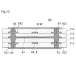
- FIG. 12 is a cross-sectional view of the multilayer board 80 according to the third example of the fourth embodiment.
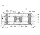
- FIG. 13 is a cross-sectional view of the multilayer board 90 according to the fifth embodiment.
- FIG. 14 is a cross-sectional view of the multilayer board 100 according to the sixth embodiment.
- FIG. 15 is a cross-sectional view of the multilayer board 110 according to the seventh embodiment.
- FIG. 16 is a plan view of the interlayer connection conductors 16a to 16c and the type 2 conductor patterns 94a to 94c in the stacking direction.
- FIG. 17 is a cross-sectional view of the multilayer board 110 according to the seventh embodiment.
- FIG. 18 is a top view of the thermoplastic resin layer 111.
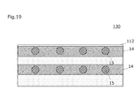
- FIG. 19 is a top view of the thermoplastic resin layer 112.
- FIG. 20 is a top view of the thermoplastic resin layer 112.
- FIG. 1 is an exploded perspective view of a part of the multilayer board 10 according to the first embodiment.
- FIG. 2 is a cross-sectional view of the multilayer board 10 according to the first embodiment.
- the multilayer board 10 is a signal transmission line.
- the multilayer substrate 10 includes a plurality of thermoplastic resin layers 111, 112, 113, 114, 115 including a thermoplastic resin layer 112 (first thermoplastic resin layer) and a thermoplastic resin layer 113 (second thermoplastic resin layer). It is made by stacking.
- the multilayer substrate 10 includes a plurality of laminated thermoplastic resin layers 111, 112, 113, 114, 115, a first-class conductor pattern 12, a second-class conductor pattern 14, and an interlayer connection conductor 15.
- the thermoplastic resin layer 112 is an example of the "first thermoplastic resin layer” of the present invention.
- the thermoplastic resin layer 113 is an example of the “second thermoplastic resin layer” of the present invention.
- the thermoplastic resin layer 113 is in contact with the other surface (second main surface M2) of the thermoplastic resin layer 112.
- the first-class conductor pattern 12 is formed of a conductor foil.
- the second-class conductor pattern 14 and the interlayer connection conductor 15 are formed of a conductive member of the same material including resin.
- the first-class conductor pattern 12 includes the first-class conductor pattern 13 formed on one surface (first main surface M1) of the thermoplastic resin layer 112.
- the interlayer connecting conductor 15 includes an interlayer connecting conductor 16 formed on the thermoplastic resin layer 112.
- the interlayer connecting conductor 16 is an example of the "first interlayer connecting conductor" of the present invention.
- One surface (first main surface m1) of the second type conductor pattern 14 is arranged so as to be in contact with the other surface (second main surface M2) of the thermoplastic resin layer 112.
- the interlayer connection conductor 16 is connected to the first-class conductor pattern 13 at one end face (first end face E1) and to the second-class conductor pattern 14 at the other end face (second end face E2).
- the area of the second end surface E2 of the interlayer connecting conductor 16 is larger than that of the first end surface E1 of the interlayer connecting conductor 16. There is no conductor pattern formed of the conductor foil between the other surface (second main surface m2) of the second type conductor pattern 14 and one surface (first main surface M11) of the thermoplastic resin layer 113.
- thermoplastic resin layers 111 to 115 are laminated in this order and are directly bonded by heating and pressurizing.
- the thermoplastic resin layers 111 to 115 are made of liquid crystal polymer (LCP) resin, polyether ether ketone (PEEK) resin, polyetherimide (PEI) resin, polyimide (PI) resin, fluororesin, and other thermoplastic resin materials. It is formed.
- the first-class conductor pattern 12 is arranged on the main surface of the thermoplastic resin layers 111 to 115.
- the first-class conductor pattern 12 is not formed on the second main surface M2 of the thermoplastic resin layer 112, and is therefore not formed between the thermoplastic resin layer 112 and the thermoplastic resin layer 113.
- the first-class conductor pattern 12 formed on the other surface of the thermoplastic resin 113 is a signal conductor layer 25a through which a high-frequency signal is transmitted.
- the first-class conductor pattern 12 formed on one surface of the thermoplastic resin 112 is a signal conductor layer 25b through which a high-frequency signal is transmitted.
- a ground potential is connected to the other type 1 conductor pattern 12.
- the first-class conductor pattern 12 is formed of, for example, a metal foil such as a copper foil.
- the interlayer connecting conductor 15 is formed on the thermoplastic resin layers 111 to 115. Each interlayer connecting conductor 15 penetrates one layer of the thermoplastic resin layers 111 to 115.
- the interlayer connecting conductor 15 has a tapered shape and is tapered in the stacking direction of the thermoplastic resin layers 111 to 115. The direction of tapering is opposite between the interlayer connecting conductors 15 arranged in the thermoplastic resin layers 111 and 112 and the interlayer connecting conductors 15 arranged in the thermoplastic resin layers 113 to 115.
- the interlayer connection conductor 15 is a solidified conductive paste by heating and pressurizing.
- the constituent material of the conductive paste is, for example, a metal powder containing Sn, Ni, Cu, Ag or an alloy thereof, a binder resin such as an epoxy resin, a solvent or the like.
- the interlayer connecting conductor 15 is formed of a conductive member containing a resin.
- the interlayer connection conductor 15 may be formed of a conductive member containing a metal having a melting point lower than that of the conductor foil.
- a conductive member is, for example, solder.
- the solder contains Pb and Sn. However, the solder does not have to contain Pb.
- the second-class conductor pattern 14 is arranged between the thermoplastic resin layer 112 and the thermoplastic resin layer 113.
- the second-class conductor pattern 14 is formed so as to cover a part of the second main surface M2 of the thermoplastic resin layer 112.
- the area of the portion of the Type 2 conductor pattern 14 that does not overlap with the interlayer connecting conductor 16 is larger than the area of the portion of the Type 2 conductor pattern 14 that overlaps with the interlayer connecting conductor 16 when viewed from the stacking direction of the thermoplastic resin layers 111 to 115. big.
- the second-class conductor pattern 14 is a solidified conductive paste by heating and pressurizing, similarly to the interlayer connecting conductor 15.
- the second-class conductor pattern 14 and the interlayer connection conductor 16 are connected to each other and are integrally formed of the same conductive member. Therefore, the second-class conductor pattern 14 may be formed of a conductive member containing a metal having a melting point lower than that of the conductor foil. A ground potential is connected to the second conductor pattern 14.
- the type 2 conductor pattern 14 is thinner than the type 1 conductor pattern 12, but may have the same thickness as the type 1 conductor pattern 12, or may be thicker than the type 1 conductor pattern 12.
- FIG. 3A is a plan view of the second type conductor pattern 14.
- 3 (B), 3 (C), 3 (D), and 3 (E) are plan views showing other examples of the type 2 conductor pattern formed on the multilayer substrate 10.
- the positions of the interlayer connecting conductors connected to the type 2 conductor pattern are shown by broken lines.
- the type 2 conductor pattern 14 is a wiring conductor pattern connecting the interlayer connection conductors 15.
- the type 2 conductor pattern formed on the multilayer substrate 10 is a spiral or coil-shaped inductor conductor pattern, a meander-shaped inductor conductor pattern, and the like.
- it may be a planar conductor pattern for a capacitor that is capacitively coupled at the end face.
- FIG. 4 is a cross-sectional view of the multilayer substrate 90 according to the modified example of the first embodiment.
- the multilayer board 90 differs from the multilayer board 10 in the following points. That is, the multilayer board 90 includes the thermoplastic resin layer 912 instead of the thermoplastic resin layer 112.
- the thermoplastic resin layer 912 is formed of a plurality of layers including the thermoplastic resin layers 9121 and 9122.
- the thermoplastic resin layers 111, 113 to 115, 9121 are LCP resin layers
- the thermoplastic resin layer 9122 is a fluororesin layer.
- the thermoplastic resin layer arranged between the type 1 conductor pattern 13 and the type 2 conductor pattern 14 may be formed of a plurality of layers.
- 5 (A), 5 (B), and 5 (C) are cross-sectional views showing a method of manufacturing the multilayer substrate 10 according to the first embodiment.
- a conductor foil is formed on one surface (first main surface M1) of the resin sheet 312 formed of a thermoplastic resin.
- the conductor foil is patterned by a photolithography technique to form a first-class conductor pattern 12.
- a hole 21 penetrating from the other surface (second main surface M2) of the resin sheet 312 to the conductor foil thereof is formed by, for example, laser processing.
- the hole 21 penetrates the resin sheet 312 but does not penetrate the first-class conductor pattern 12, and exposes the first-class conductor pattern 12 at the bottom thereof. Since the holes 21 are opened from the second main surface M2 side of the resin sheet 312, the holes 21 taper from the second main surface M2 side of the resin sheet 312 toward the first main surface M1 side.
- the step of patterning the conductor foil may be performed before or after the step of forming the hole 21, or may be performed in parallel with the step of forming the hole 21.
- the holes 21 are filled with the conductive paste to form the conductive paste body 35, and the conductive paste is used on the second main surface M2 of the resin sheet 312.
- the conductive paste body 34 is an example of the "conductive pattern" of the present invention.
- the conductive paste bodies 34 and 35 are formed by printing or spraying the conductive paste on the second main surface M2 of the resin sheet 312.
- the conductive paste body 34 is connected to at least one of the conductive paste bodies 35 and covers a part of the second main surface M2 of the resin sheet 312.
- the conductive paste bodies 34 and 35 are formed of the same conductive paste.
- the conductive paste body 34 is thinner than the first-class conductor pattern 12, it may have the same thickness as the first-class conductor pattern 12 or may be thicker than the first-class conductor pattern 12.
- the resin sheets 311, 313, 314, The first-class conductor pattern 12 and the conductive paste body 35 are formed on the 315.
- the conductive paste body 34 may be formed on the resin sheet 313 instead of the resin sheet 312. ..
- the materials of the resin sheets 313 to 315 are LCP resin, PEEK resin, PEI resin, PI resin, fluororesin, and other thermoplastic resins.
- the conductor foil is, for example, a metal foil such as a copper foil.
- the constituent material of the conductive paste is, for example, a metal powder containing Sn, Ni, Cu, Ag or an alloy thereof, a binder resin such as an epoxy resin, a solvent or the like.
- the metal body may be formed of a conductive member containing a metal having a melting point lower than that of the conductor foil.
- the conductive member containing a metal having a melting point lower than that of the conductor foil is, for example, solder.
- the main surface on which the first-class conductor pattern 12 is formed on the resin sheets 313 to 315 is the main surface on which the first-class conductor pattern 12 is formed on the resin sheets 311, 312.
- the resin sheets 311 to 315 are laminated in this order toward the side opposite to the surface. More simply, the resin sheets 311 to 315 are laminated by reversing the orientation of the resin sheets 313 to 315 with respect to the direction of the resin sheets 311, 312.
- the resin sheets 311 to 315 are thermocompression bonded together, and the conductive paste body 34 is solidified to form the second type conductor pattern 14, which is conductive.
- the sex paste body 35 is solidified to form the interlayer connecting conductor 15. As a result, the multilayer board 10 is obtained.
- individual multilayer boards 10 may be manufactured by separating the aggregated boards having the structure of the plurality of multilayer boards 10 into individual pieces.
- the type 2 conductor pattern 14 is formed of a conductive member made of the same material as the interlayer connecting conductor 16, the connection reliability between the conductor pattern and the interlayer connecting conductor is improved.
- a conductor pattern is formed at a portion where resin sheets whose lamination directions are reversed from each other are joined to each other (hereinafter referred to as an inverted portion). It's not easy to do.
- the second type conductor pattern 14 is formed from the same material as the interlayer connecting conductor 15 in the step of forming the interlayer connecting conductor 15. Therefore, it is possible to form a conductor pattern at the inverted portion without complicating the manufacturing process and suppressing an increase in the number of processes.
- the number of layers of the conductor pattern can be increased without changing the number of layers of the thermoplastic resin layer, and therefore the wiring density of the multilayer board can be increased.
- the number of layers of the thermoplastic resin layer in the conventional multilayer board is changed to the first embodiment.
- the number of layers of the thermoplastic resin layer in the multilayer board can be reduced.
- the type 2 conductor pattern 14 is thinner than the type 1 conductor pattern 12. This indicates that the conductive paste body 34 is formed thinner than the first-class conductor pattern 12. Therefore, in the steps of heating and pressurizing the laminated resin sheets 311 to 315, the exudation or flow of the conductive paste body 34 is relatively suppressed, and the dimensional error of the second-class conductor pattern 14 is relatively suppressed. Be done.
- the conductive pattern to be the second type conductor pattern is printed while filling the holes with the conductive paste or the metal cream.
- the metal cream is, for example, a mixture of metal and liquid flux.
- the interlayer connecting conductor 16 and the type 2 conductor pattern 14 can be formed at the same time.
- the conductive paste and the metal cream are difficult to fall off.
- the multilayer board 10 can be easily manufactured.
- the conductive paste or metal cream filled in the pores and the conductive pattern are simultaneously solidified by heating.
- the interlayer connection conductor 16 and the second-class conductor pattern 14 are simultaneously formed in a state where the conductive paste or metal cream filled in the pores and the conductive pattern are connected to each other. As a result, the connection reliability between the interlayer connection conductor 16 and the type 2 conductor pattern 14 is improved.
- thermoplastic resin layer has a recess for accommodating the second type conductor pattern.
- FIG. 6 is a cross-sectional view of the multilayer board 40 according to the second embodiment.
- the multilayer board 40 differs from the multilayer board 10 (see FIG. 2) according to the first embodiment in the following points. That is, the thermoplastic resin layer 112 of the multilayer board 40 has a recess (or groove) 22.
- the recess 22 is formed on the second main surface M2 of the thermoplastic resin layer 112.
- the recess 22 is formed along the type 2 conductor pattern 14 and accommodates the type 2 conductor pattern 14.
- the side surface S1 of the second-class conductor pattern 14 is in contact with the thermoplastic resin layer 112.
- the recess 22 accommodating the type 2 conductor pattern 14 may be formed not on the second main surface M2 of the thermoplastic resin layer 112 but on the main surface of the thermoplastic resin layer 113 in contact with the thermoplastic resin layer 112. ..
- the roughness of the bottom surface and the side surface of the recess 22 is different from the roughness of the portion of the second main surface M2 of the thermoplastic resin layer 112 where the recess is not formed.
- the roughness of the bottom surface and the side surface of the recess 22 is the roughness of the portion of the second main surface M2 of the thermoplastic resin layer 112 where the recess is not formed. Greater than degree.
- the arithmetic mean roughness is used as an index of roughness.
- 7 (A), 7 (B) and 7 (C) are cross-sectional views showing a method of manufacturing the multilayer substrate 40 according to the second embodiment.
- the first-class conductor pattern 12 and the holes 21 are formed on the resin sheet 312 by the same steps as the steps of the manufacturing method according to the first embodiment. Further, a recess 22 is formed in the second main surface M2 of the resin sheet 312. For example, the recess 22 is formed by etching, laser, or cutting.
- the holes 21 are filled with the conductive paste to form the conductive paste body 35, and the concave portions 22 are filled with the conductive paste to form the conductive paste body 34.
- the conductive paste bodies 34 and 35 are formed by printing or spraying the conductive paste on the second main surface M2 of the resin sheet 312.
- the first-class conductor pattern 12 and the conductive paste body 35 are formed on the resin sheets 311, 313 to 315 by the same steps as those of the manufacturing method according to the first embodiment. , And the resin sheets 311 to 315 are laminated and heated and pressed. As a result, the multilayer board 40 is obtained.
- the concave portion 22 of the resin sheet 312 is filled with the conductive paste to form the second type conductor pattern 14. Therefore, the crushing or squeezing of the conductive paste is suppressed in the heating and pressurizing steps.
- the dimensional error of the second type conductor pattern 14 can be suppressed. In other words, the migration of the second type conductor pattern 14 is suppressed.
- the type 2 conductor pattern 14 can be made thicker while suppressing the dimensional error of the type 2 conductor pattern 14.
- a conductor pattern constituting an element required to have a predetermined characteristic such as an inductor or a capacitor may be formed. Strict dimensional errors are required for such conductor patterns. Therefore, it is particularly effective to form such a conductor pattern by using the type 2 conductor pattern housed in the recess.
- Third Embodiment a wall portion surrounding the type 2 conductor pattern is provided.
- FIG. 8 is a cross-sectional view of the multilayer board 50 according to the third embodiment.
- the multilayer board 50 differs from the multilayer board 10 (see FIG. 2) according to the first embodiment in the following points. That is, the multilayer substrate 50 includes a wall portion 23 formed on the second main surface M2 of the thermoplastic resin layer 112.
- the wall portion 23 surrounds the type 2 conductor pattern 14 when viewed from the stacking direction of the thermoplastic resin layers 111 to 115.
- the wall portion 23 does not extend to the ends of the thermoplastic resin layers 111 to 115. In other words, the wall portion 23 is not exposed to the outside.
- the wall portion 23 may extend to the ends of the thermoplastic resin layers 111 to 115.
- the wall portion 23 may be formed of a magnetic material.
- the magnetic material can be placed inside the inductor by forming the wall portion 23, so that the inductance value increases.
- 9 (A), 9 (B) and 9 (C) are cross-sectional views showing a method of manufacturing the multilayer substrate 50 according to the third embodiment.
- the first-class conductor pattern 12 and the holes 21 are formed on the resin sheet 312 by the same steps as the steps of the manufacturing method according to the first embodiment. Further, the wall portion 23 is formed on the second main surface M2 of the resin sheet 312.
- the conductive paste body 35 is formed in the holes 21 and the wall portion 23 is formed.
- the conductive paste body 34 is formed in the space surrounded by.
- the first-class conductor pattern 12 and the conductive paste body 35 are formed on the resin sheets 311, 313 to 315 by the same steps as those of the manufacturing method according to the first embodiment. , And the resin sheets 311 to 315 are laminated and heated and pressed. As a result, the multilayer board 50 is obtained.
- the second type conductor pattern 14 is formed by filling the space surrounded by the wall portion 23 with the conductive paste. Therefore, in the heating and pressurizing steps, the crushing or squeezing of the conductive paste is suppressed, and the dimensional error of the type 2 conductor pattern 14 is suppressed.
- the wall portion 23 does not extend to the ends of the thermoplastic resin layers 111 to 115. Therefore, in the heating and pressurizing steps, the wall portion 23 is sandwiched between the resin sheet 312 and the resin sheet 313, so that the wall portion 23 is less likely to be peeled off from the resin sheet 312.
- the second type conductor pattern is used for the bridge wiring connecting the two signal conductors.
- the second type conductor pattern is utilized for the electrode of the capacitor.
- the second type conductor pattern is used as a shield conductor that electromagnetically shields the signal conductor from each other.
- FIG. 10 is a cross-sectional view of the multilayer board 60 according to the first example of the fourth embodiment.
- the multilayer board 60 includes thermoplastic resin layers 111 to 114, first-class conductor patterns 6211, 6212, 622, second-class conductor patterns 64, and interlayer connection conductors 651, 6521, 6522. These components make up two strip lines.
- the first-class conductor patterns 6211 and 6212 constitute the first and second signal conductors, respectively.
- the first-class conductor pattern 622 and the interlayer connecting conductor 651 constitute a ground conductor.
- the second-class conductor pattern 64 and the interlayer connection conductors 6521 and 6522 constitute a bridge wiring connecting the first signal conductor and the second signal conductor.
- the interlayer connecting conductors 6521 and 6522 are examples of the "first interlayer connecting conductor" and the "second interlayer connecting conductor" of the present invention, respectively.
- the resistivity of the type 1 conductor pattern is smaller than the resistivity of the type 2 conductor pattern. Therefore, it is preferable to use the first-class conductor pattern for the signal conductor.
- the first-class conductor patterns 6211 and 6212 are formed on the first main surface M1 of the thermoplastic resin layer 112.
- the interlayer connection conductors 6521 and 6522 are formed on the thermoplastic resin layer 112 and are connected to the first-class conductor patterns 6211 and 6212, respectively.
- the second-class conductor pattern 64 is formed on the second main surface M2 of the thermoplastic resin layer 112, and connects the interlayer connecting conductor 6521 and the interlayer connecting conductor 6522.
- the first-class conductor patterns 6211, 6212, 622 are formed of a conductor foil, and the second-class conductor pattern 64 and the interlayer connection conductors 651, 6521, 6522 are formed of a conductive member made of the same material.
- FIG. 11 is a cross-sectional view of the multilayer substrate 70 according to the second example of the fourth embodiment.
- the multilayer board 70 includes thermoplastic resin layers 111 to 115, a first-class conductor pattern 721, 722, a second-class conductor pattern 74, and an interlayer connection conductor 751, 752. These components make up the capacitor.
- the first-class conductor pattern 721, the second-class conductor pattern 74, and the interlayer connection conductor 751 constitute one electrode of the capacitor.
- the first-class conductor pattern 722 and the interlayer connection conductor 752 constitute the other electrode of the capacitor.
- the first-class conductor patterns 721 and 722 are formed of a conductor foil, and the second-class conductor pattern 74 and the interlayer connection conductors 751 and 752 are formed of a conductive member made of the same material.
- FIG. 12 is a cross-sectional view of the multilayer board 80 according to the third example of the fourth embodiment.
- the multilayer board 80 includes thermoplastic resin layers 111 to 114, a first-class conductor pattern 8211, 8212, 822, a second-class conductor pattern 84, and an interlayer connection conductor 85. These components make up two strip lines.
- the first-class conductor patterns 8211 and 8212 constitute the first and second signal conductors, respectively.
- the first-class conductor pattern 822, the second-class conductor pattern 84, and the interlayer connecting conductor 85 constitute a ground conductor.
- the type 2 conductor pattern 84 is arranged between the first signal conductor and the second signal conductor in the stacking direction of the thermoplastic resin layers 111 to 114, and constitutes a shield conductor.
- the first-class conductor pattern 8211, 8212, 822 is formed of a conductor foil
- the second-class conductor pattern 84 and the interlayer connection conductor 85 are formed of a conductive member made of the same material.
- the multilayer board 90 further includes interlayer connecting conductors 9523, 9524.
- FIG. 13 is a cross-sectional view of the multilayer board 90 according to the fifth embodiment.
- the interlayer connecting conductors 9523 and 9524 penetrate the thermoplastic resin layer 113.
- One end of the interlayer connection conductors 9523 and 9524 is connected to the type 2 conductor pattern 94.
- the other ends of the interlayer connection conductors 9523 and 9524 are connected to the first-class conductor pattern 922.
- the area of one end of the interlayer connecting conductors 9523, 9524 is larger than the area of the other end of the interlayer connecting conductors 9523, 9524.
- interlayer connecting conductor 9521 and the interlayer connecting conductor 9522 are adjacent to each other. More specifically, the interlayer connecting conductor 9521 is located closest to the interlayer connecting conductor 9522 in a direction orthogonal to the stacking direction.
- the interlayer connecting conductor 9523 and the interlayer connecting conductor 9524 are adjacent to each other. More specifically, the interlayer connecting conductor 9523 is located closest to the interlayer connecting conductor 9524 in a direction orthogonal to the stacking direction.
- thermoplastic resin layer 112 the conductive pattern formed on one surface of the thermoplastic resin layer 112 and the conductive pattern formed on one main surface of the thermoplastic resin layer 113 are overlapped with each other to form the second type.
- a conductor pattern 94 is formed.
- the multilayer substrate 100 further includes the second type conductor patterns 94a and 94b.
- FIG. 14 is a cross-sectional view of the multilayer board 100 according to the sixth embodiment.
- the type 2 conductor pattern 94 is separated into the interlayer connecting conductor 9521 and the type 2 conductor pattern 9522, and the interlayer connecting conductor 9521 and the type 2 conductor pattern 9522 are displaced in the direction orthogonal to the stacking direction. In that respect, it differs from the multilayer board 90.
- the other ends of the interlayer connecting conductors 9521 and 9522 are connected to the type 2 conductor pattern 94a formed on the other surface of the thermoplastic resin layer 112.
- Each of one ends of the interlayer connection conductors 9521 and 9522 are connected to the first-class conductor patterns 9211 and 9212.
- the area of the other end of the interlayer connecting conductors 9521 and 9522 is larger than the area of one end of the interlayer connecting conductors 9521 and 9522.
- One end of the interlayer connection conductors 9523 and 9524 is connected to the type 2 conductor pattern 94b formed on one surface of the thermoplastic resin layer 112.
- the other ends of the interlayer connection conductors 9523 and 9524 are connected to the first-class conductor pattern 922.
- the area of one end of the interlayer connecting conductors 9523, 9524 is larger than the area of the other end of the interlayer connecting conductors 9523, 9524.
- the type 2 conductor pattern 94b is displaced in the direction orthogonal to the stacking direction with respect to the type 2 conductor pattern 94a. Therefore, a step is formed at the boundary between the type 2 conductor pattern 94a and the type 2 conductor pattern 94b.
- the multilayer board 100 as described above has the same effect as that of the multilayer board 90.
- FIG. 15 is a cross-sectional view of the multilayer board 110 according to the seventh embodiment.
- the shield region A0 is located between the first-class conductor pattern 1000 provided on one surface of the multilayer board 110 and the first-class conductor pattern 1002 provided on the other surface of the multilayer board 110. is doing. Further, interlayer connection conductors 951 are provided on both sides of the shield region A0 in the direction orthogonal to the stacking direction. The first-class conductor patterns 1000 and 1002 and the interlayer connection conductor 951 are connected to the ground potential. As a result, the shield region A0 is surrounded by the first-class conductor patterns 1000 and 1002 connected to the ground potential and the interlayer connecting conductor 951.
- An electronic circuit that is not affected by noise is provided in the shield region A0 as described above.
- Such electronic circuits are, for example, high-frequency circuits, active elements, and ICs (Integrated Circuits).
- interlayer connection conductors 951 may be connected to both ends of the type 2 conductor pattern 94a from both sides in the stacking direction, and the interlayer connection conductors 951 may be connected to both ends of the type 2 conductor pattern 94a in the stacking direction.
- the interlayer connection conductor 951 may be connected from one side or the other side.
- interlayer connection conductors 951 may be connected to both ends of the type 2 conductor pattern 94b from both sides in the stacking direction, and one side or the other side in the stacking direction may be connected to both ends of the type 2 conductor pattern 94b.
- the interlayer connection conductor 951 may be connected from the above.
- a signal conductor layer may be provided in the shield region A0 as described above.
- the presence of the second-class conductor pattern 94a between the multilayer board 110 and the end thereof suppresses noise radiation to the outside of the multilayer board 110.
- the multilayer substrate 120 includes interlayer connecting conductors 16a to 16c and type 2 conductor patterns 14a to 14c.
- FIG. 16 is a plan view of the interlayer connection conductors 16a to 16c and the type 2 conductor patterns 14a to 14c in the stacking direction.
- the interlayer connection conductors 16a to 16c penetrate the thermoplastic resin layer 112 in the stacking direction.
- the second-class conductor patterns 14a to 14c are formed on the other surface of the thermoplastic resin layer 112.
- the second-class conductor patterns 14a to 14c connect the interlayer connection conductors 16a to 16c.
- the type 2 conductor pattern 14a connects the interlayer connecting conductor 16a (first interlayer connecting conductor) and the interlayer connecting conductor 16b (second interlayer connecting conductor).
- the type 2 conductor pattern 14b connects the interlayer connecting conductor 16b (second interlayer connecting conductor) and the interlayer connecting conductor 16c (third interlayer connecting conductor).
- the type 2 conductor pattern 14c connects the interlayer connecting conductor 16c (third interlayer connecting conductor) and the interlayer connecting conductor 16a (first interlayer connecting conductor).
- the ratio of the second type conductor patterns 14a to 14c to the multilayer board 120 becomes large when viewed in the stacking direction. Therefore, when the type 2 conductor patterns 14a to 14c are connected to the ground potential, the shielding property of the multilayer board 120 is improved.
- the type 2 conductor pattern 14a and the type 2 conductor pattern 14b are connected to one. As a result, when the type 2 conductor patterns 14a and 14b are connected to the ground potential, the shielding property of the multilayer board 120 is further improved.
- the multilayer board 130 includes signal conductors 200a and 200b.
- FIG. 17 is a cross-sectional view of the multilayer board 110 according to the seventh embodiment.
- FIG. 18 is a top view of the thermoplastic resin layer 111.
- FIG. 19 is a top view of the thermoplastic resin layer 112.
- the signal conductors 200a and 200b are formed on the other surface of the thermoplastic resin layer 111. Between the signal conductor layers 200a and 200b, a plurality of interlayer connecting conductors 15 are arranged along the signal conductor layers 200a and 200b. This improves the isolation of the signal conductor layers 200a and 200b.
- the plurality of interlayer connecting conductors 15 are connected by a type 2 conductor pattern 14 provided on the thermoplastic resin layer 112.
- FIG. 20 is a top view of the thermoplastic resin layer 112.
- the interlayer connecting conductor 15 not connected to the type 2 conductor pattern 14 is located. May be good.
- the second type conductor pattern can be used to realize various electrical functions.
- the type 2 conductor pattern is not limited to a pattern having functionality, but may be a pattern only for making an electrical connection.
- a diffusion layer may be formed between the type 1 conductor pattern and the interlayer connecting conductor.
- the diffusion layer is an alloy region formed by the metal in the type 1 conductor pattern diffusing into the interlayer connecting conductor and / or the metal in the interlayer connecting conductor diffusing into the type 1 conductor pattern.
- the type 1 conductor pattern may include a rust preventive layer.
- the rust preventive layer contains, for example, Ni and W.
- the rust preventive layer is provided on the surface of a copper foil, which is an example of a metal foil, for example.
- the rust preventive layer existing on the bottom surface of the hole may be completely removed. Further, a part of the rust preventive layer existing on the bottom surface of the hole may remain. When all the rust preventive layers are removed, the first-class conductor pattern and the interlayer connecting conductor are more reliably connected.
- the type 2 conductor pattern may be arranged between the first signal conductor and the second signal conductor. Therefore, the type 2 conductor pattern may be arranged between the first signal conductor and the second signal conductor in the stacking direction, or the first signal conductor and the second signal conductor in the direction orthogonal to the stacking direction. It may be arranged between.
Landscapes
- Engineering & Computer Science (AREA)
- Microelectronics & Electronic Packaging (AREA)
- Manufacturing & Machinery (AREA)
- Chemical & Material Sciences (AREA)
- Dispersion Chemistry (AREA)
- Production Of Multi-Layered Print Wiring Board (AREA)
Priority Applications (3)
| Application Number | Priority Date | Filing Date | Title |
|---|---|---|---|
| CN202190000490.9U CN219204859U (zh) | 2020-06-03 | 2021-06-03 | 多层基板 |
| JP2022528882A JP7338793B2 (ja) | 2020-06-03 | 2021-06-03 | 多層基板及びその製造方法 |
| US17/979,032 US12336093B2 (en) | 2020-06-03 | 2022-11-02 | Multilayer board and method of manufacturing the same |
Applications Claiming Priority (2)
| Application Number | Priority Date | Filing Date | Title |
|---|---|---|---|
| JP2020-096562 | 2020-06-03 | ||
| JP2020096562 | 2020-06-03 |
Related Child Applications (1)
| Application Number | Title | Priority Date | Filing Date |
|---|---|---|---|
| US17/979,032 Continuation US12336093B2 (en) | 2020-06-03 | 2022-11-02 | Multilayer board and method of manufacturing the same |
Publications (1)
| Publication Number | Publication Date |
|---|---|
| WO2021246467A1 true WO2021246467A1 (ja) | 2021-12-09 |
Family
ID=78831224
Family Applications (1)
| Application Number | Title | Priority Date | Filing Date |
|---|---|---|---|
| PCT/JP2021/021109 Ceased WO2021246467A1 (ja) | 2020-06-03 | 2021-06-03 | 多層基板及びその製造方法 |
Country Status (4)
| Country | Link |
|---|---|
| US (1) | US12336093B2 (https=) |
| JP (1) | JP7338793B2 (https=) |
| CN (1) | CN219204859U (https=) |
| WO (1) | WO2021246467A1 (https=) |
Cited By (3)
| Publication number | Priority date | Publication date | Assignee | Title |
|---|---|---|---|---|
| WO2024219282A1 (ja) * | 2023-04-20 | 2024-10-24 | 株式会社村田製作所 | 回路基板及び回路基板の製造方法 |
| US12148688B2 (en) | 2023-02-13 | 2024-11-19 | Dyi-chung Hu | Semiconductor substrate and manufacturing method thereof |
| TWI884561B (zh) * | 2023-02-13 | 2025-05-21 | 胡迪群 | 半導體基板及其製造方法 |
Families Citing this family (1)
| Publication number | Priority date | Publication date | Assignee | Title |
|---|---|---|---|---|
| WO2026048351A1 (ja) * | 2024-09-02 | 2026-03-05 | 日東電工株式会社 | フレキシブル多層回路基板 |
Citations (2)
| Publication number | Priority date | Publication date | Assignee | Title |
|---|---|---|---|---|
| JP2005251949A (ja) * | 2004-03-03 | 2005-09-15 | Sony Corp | 配線基板及びその製造方法 |
| JP2016213416A (ja) * | 2015-05-13 | 2016-12-15 | 株式会社村田製作所 | 樹脂多層基板およびその製造方法 |
Family Cites Families (11)
| Publication number | Priority date | Publication date | Assignee | Title |
|---|---|---|---|---|
| JP4186756B2 (ja) * | 2003-08-29 | 2008-11-26 | 松下電器産業株式会社 | 回路基板及びその製造方法 |
| US6908960B2 (en) * | 1999-12-28 | 2005-06-21 | Tdk Corporation | Composite dielectric material, composite dielectric substrate, prepreg, coated metal foil, molded sheet, composite magnetic substrate, substrate, double side metal foil-clad substrate, flame retardant substrate, polyvinylbenzyl ether resin composition, thermosettin |
| JP2002026520A (ja) | 2000-07-06 | 2002-01-25 | Matsushita Electric Ind Co Ltd | 多層配線基板及びその製造方法 |
| TW550997B (en) * | 2001-10-18 | 2003-09-01 | Matsushita Electric Industrial Co Ltd | Module with built-in components and the manufacturing method thereof |
| JP4181778B2 (ja) * | 2002-02-05 | 2008-11-19 | ソニー株式会社 | 配線基板の製造方法 |
| JP5293060B2 (ja) * | 2008-10-02 | 2013-09-18 | 株式会社デンソー | 多層回路基板およびその製造方法 |
| WO2011058938A1 (ja) * | 2009-11-10 | 2011-05-19 | 株式会社村田製作所 | 多層基板およびその製造方法 |
| CN103329637B (zh) | 2011-02-08 | 2016-04-13 | 株式会社村田制作所 | 树脂多层基板及其制造方法 |
| CN103430639B (zh) * | 2011-03-17 | 2016-09-28 | 株式会社村田制作所 | 树脂多层基板 |
| EP3926756A4 (en) * | 2019-02-13 | 2022-11-09 | The University of Tokyo | CIRCUIT SUBSTRATE, ANTENNA ELEMENT, MILLIMETER WAVE ABSORBER FOR INCORPORATION INTO A SUBSTRATE AND METHOD OF NOISE REDUCTION IN A CIRCUIT SUBSTRATE |
| JP7325891B2 (ja) * | 2019-10-24 | 2023-08-15 | エルジー・ケム・リミテッド | 多層印刷回路基板用絶縁層、これを含む多層印刷回路基板およびその製造方法 |
-
2021
- 2021-06-03 WO PCT/JP2021/021109 patent/WO2021246467A1/ja not_active Ceased
- 2021-06-03 JP JP2022528882A patent/JP7338793B2/ja active Active
- 2021-06-03 CN CN202190000490.9U patent/CN219204859U/zh active Active
-
2022
- 2022-11-02 US US17/979,032 patent/US12336093B2/en active Active
Patent Citations (2)
| Publication number | Priority date | Publication date | Assignee | Title |
|---|---|---|---|---|
| JP2005251949A (ja) * | 2004-03-03 | 2005-09-15 | Sony Corp | 配線基板及びその製造方法 |
| JP2016213416A (ja) * | 2015-05-13 | 2016-12-15 | 株式会社村田製作所 | 樹脂多層基板およびその製造方法 |
Cited By (3)
| Publication number | Priority date | Publication date | Assignee | Title |
|---|---|---|---|---|
| US12148688B2 (en) | 2023-02-13 | 2024-11-19 | Dyi-chung Hu | Semiconductor substrate and manufacturing method thereof |
| TWI884561B (zh) * | 2023-02-13 | 2025-05-21 | 胡迪群 | 半導體基板及其製造方法 |
| WO2024219282A1 (ja) * | 2023-04-20 | 2024-10-24 | 株式会社村田製作所 | 回路基板及び回路基板の製造方法 |
Also Published As
| Publication number | Publication date |
|---|---|
| JP7338793B2 (ja) | 2023-09-05 |
| US12336093B2 (en) | 2025-06-17 |
| CN219204859U (zh) | 2023-06-16 |
| JPWO2021246467A1 (https=) | 2021-12-09 |
| US20230053211A1 (en) | 2023-02-16 |
Similar Documents
| Publication | Publication Date | Title |
|---|---|---|
| WO2021246467A1 (ja) | 多層基板及びその製造方法 | |
| JP5333680B2 (ja) | 部品内蔵基板およびその製造方法 | |
| JP7001158B2 (ja) | 多層基板、電子機器および多層基板の製造方法 | |
| US10886057B2 (en) | Electronic component | |
| JP5652481B2 (ja) | 樹脂多層基板およびその製造方法 | |
| US9012785B2 (en) | Flexible multilayer substrate | |
| JPWO2012137626A1 (ja) | 部品内蔵樹脂基板およびその製造方法 | |
| WO2015033736A1 (ja) | 多層基板 | |
| JP2018186241A (ja) | 電子部品およびその製造方法 | |
| US20210065975A1 (en) | Method for producing multilayer coil component and multilayer coil component | |
| US20110108315A1 (en) | Process for fabricating circuit substrate, and circuit substrate | |
| US20200288574A1 (en) | Multilayer substrate, multilayer substrate mounting structure, method of manufacturing multilayer substrate, and method of manufacturing electronic device | |
| WO2019098011A1 (ja) | 樹脂多層基板、電子部品およびその実装構造 | |
| JP2005026313A (ja) | 配線基板の製造方法 | |
| JP2000151041A (ja) | プリント配線板 | |
| CN207124812U (zh) | 线圈内置基板 | |
| JP5741975B2 (ja) | 樹脂多層基板 | |
| JP2019021863A (ja) | 多層基板 | |
| WO2018037871A1 (ja) | 樹脂多層基板、伝送線路、モジュールおよびモジュールの製造方法 | |
| CN107889356B (zh) | 软硬复合线路板 | |
| JP2005123332A (ja) | 回路基板及びその製造方法 | |
| CN211828497U (zh) | 树脂多层基板以及电子设备 | |
| JP6438059B2 (ja) | アンテナ装置及びその製造方法 | |
| JP7197058B2 (ja) | 回路基板、回路基板の接続構造、および、回路基板の接続構造の製造方法 | |
| US7638882B2 (en) | Flip-chip package and method of forming thereof |
Legal Events
| Date | Code | Title | Description |
|---|---|---|---|
| 121 | Ep: the epo has been informed by wipo that ep was designated in this application |
Ref document number: 21818185 Country of ref document: EP Kind code of ref document: A1 |
|
| ENP | Entry into the national phase |
Ref document number: 2022528882 Country of ref document: JP Kind code of ref document: A |
|
| NENP | Non-entry into the national phase |
Ref country code: DE |
|
| 122 | Ep: pct application non-entry in european phase |
Ref document number: 21818185 Country of ref document: EP Kind code of ref document: A1 |