WO2021241208A1 - Lcフィルタ - Google Patents
Lcフィルタ Download PDFInfo
- Publication number
- WO2021241208A1 WO2021241208A1 PCT/JP2021/017900 JP2021017900W WO2021241208A1 WO 2021241208 A1 WO2021241208 A1 WO 2021241208A1 JP 2021017900 W JP2021017900 W JP 2021017900W WO 2021241208 A1 WO2021241208 A1 WO 2021241208A1
- Authority
- WO
- WIPO (PCT)
- Prior art keywords
- electrode
- inductor
- filter
- ground
- inductor via
- Prior art date
- Legal status (The legal status is an assumption and is not a legal conclusion. Google has not performed a legal analysis and makes no representation as to the accuracy of the status listed.)
- Ceased
Links
Images





Classifications
-
- H—ELECTRICITY
- H03—ELECTRONIC CIRCUITRY
- H03H—IMPEDANCE NETWORKS, e.g. RESONANT CIRCUITS; RESONATORS
- H03H7/00—Multiple-port networks comprising only passive electrical elements as network components
- H03H7/01—Frequency selective two-port networks
- H03H7/0115—Frequency selective two-port networks comprising only inductors and capacitors
-
- H—ELECTRICITY
- H03—ELECTRONIC CIRCUITRY
- H03H—IMPEDANCE NETWORKS, e.g. RESONANT CIRCUITS; RESONATORS
- H03H7/00—Multiple-port networks comprising only passive electrical elements as network components
- H03H7/01—Frequency selective two-port networks
- H03H7/03—Frequency selective two-port networks comprising means for compensation of loss
-
- H—ELECTRICITY
- H01—ELECTRIC ELEMENTS
- H01F—MAGNETS; INDUCTANCES; TRANSFORMERS; SELECTION OF MATERIALS FOR THEIR MAGNETIC PROPERTIES
- H01F27/00—Details of transformers or inductances, in general
-
- H—ELECTRICITY
- H01—ELECTRIC ELEMENTS
- H01G—CAPACITORS; CAPACITORS, RECTIFIERS, DETECTORS, SWITCHING DEVICES, LIGHT-SENSITIVE OR TEMPERATURE-SENSITIVE DEVICES OF THE ELECTROLYTIC TYPE
- H01G4/00—Fixed capacitors; Processes of their manufacture
- H01G4/40—Structural combinations of fixed capacitors with other electric elements, the structure mainly consisting of a capacitor, e.g. RC combinations
-
- H—ELECTRICITY
- H03—ELECTRONIC CIRCUITRY
- H03H—IMPEDANCE NETWORKS, e.g. RESONANT CIRCUITS; RESONATORS
- H03H1/00—Constructional details of impedance networks whose electrical mode of operation is not specified or applicable to more than one type of network
-
- H—ELECTRICITY
- H03—ELECTRONIC CIRCUITRY
- H03H—IMPEDANCE NETWORKS, e.g. RESONANT CIRCUITS; RESONATORS
- H03H7/00—Multiple-port networks comprising only passive electrical elements as network components
- H03H7/01—Frequency selective two-port networks
- H03H7/0138—Electrical filters or coupling circuits
-
- H—ELECTRICITY
- H03—ELECTRONIC CIRCUITRY
- H03H—IMPEDANCE NETWORKS, e.g. RESONANT CIRCUITS; RESONATORS
- H03H7/00—Multiple-port networks comprising only passive electrical elements as network components
- H03H7/01—Frequency selective two-port networks
- H03H7/0153—Electrical filters; Controlling thereof
- H03H7/0161—Bandpass filters
-
- H—ELECTRICITY
- H03—ELECTRONIC CIRCUITRY
- H03H—IMPEDANCE NETWORKS, e.g. RESONANT CIRCUITS; RESONATORS
- H03H7/00—Multiple-port networks comprising only passive electrical elements as network components
- H03H7/01—Frequency selective two-port networks
- H03H7/17—Structural details of sub-circuits of frequency selective networks
- H03H7/1741—Comprising typical LC combinations, irrespective of presence and location of additional resistors
-
- H—ELECTRICITY
- H03—ELECTRONIC CIRCUITRY
- H03H—IMPEDANCE NETWORKS, e.g. RESONANT CIRCUITS; RESONATORS
- H03H1/00—Constructional details of impedance networks whose electrical mode of operation is not specified or applicable to more than one type of network
- H03H2001/0021—Constructional details
- H03H2001/0085—Multilayer, e.g. LTCC, HTCC, green sheets
Definitions
- the present disclosure relates to an LC filter, and more specifically, to a technique for improving the characteristics of a laminated LC filter.
- Patent Document 1 discloses an LC filter in which a multi-stage resonator composed of an inductor and a capacitor is formed in a multilayer substrate.
- the resonator of each stage is magnetically coupled and / or capacitively coupled to other adjacent resonators to obtain desired filter characteristics. Has been realized.
- the LC filter as described above may be used in a portable communication device represented by a mobile phone or a smartphone.
- a portable communication device represented by a mobile phone or a smartphone.
- Patent Document 1 In an LC filter having a multi-stage resonator as disclosed in Japanese Patent Application Laid-Open No. 2000-165171 (Patent Document 1), the attenuation characteristic in the non-passband is improved by increasing the number of stages of the resonator. Is known to be possible. However, if the number of resonators formed in the laminate increases, the coupling between the resonators will be strengthened, and although the filter loss will decrease, the signal in the non-passband may not be sufficiently attenuated. There is.
- the present disclosure has been made to solve such a problem, and an object thereof is to improve the attenuation characteristics of a multi-stage laminated LC filter while suppressing an increase in filter loss.
- the LC filter according to the present disclosure includes an input terminal, an output terminal, a laminate including a plurality of dielectric layers, a first electrode and a second electrode, and a connection electrode connecting the first electrode and the second electrode.
- the first electrode and the second electrode are provided on different dielectric layers in the laminated body.
- the first capacitor electrode, the second capacitor electrode, the third capacitor electrode, and the fourth capacitor electrode face the second electrode.
- the first capacitor electrode is connected to the first inductor via.
- the second capacitor electrode is connected to the second inductor via.
- the third capacitor electrode is connected to the third inductor via.
- the fourth capacitor electrode is connected to the fourth inductor via.
- One end of the first inductor via is connected to the input terminal via the first capacitor electrode.
- the other end of the first inductor via is connected at a position on the connection electrode between the first electrode and the second electrode.
- the second inductor via is connected between the first electrode and the second capacitor electrode.
- the third inductor via is connected between the first electrode and the third capacitor electrode.
- One end of the fourth inductor via is connected to the output terminal via the fourth capacitor electrode.
- the other end of the fourth inductor via is connected at a position on the connection electrode between the first electrode and the second electrode.
- the resonant circuit connected to the input / output terminal is directly connected to the connecting electrode connecting the first electrode and the second electrode. .. This weakens the magnetic coupling due to the resonant circuit connected to the input / output terminals. Therefore, it is possible to improve the attenuation characteristics while suppressing the increase in the loss of the filter.
- FIG. 1 It is a perspective perspective view of the LC filter according to Embodiment 1.
- FIG. 2 It is a side perspective view of the LC filter of FIG. It is a top view for demonstrating the transmission path of the signal (current) in the plate electrode PG1 of the LC filter of FIG.
- FIG. 2 It is a perspective view of the LC filter of the modification 1.
- FIG. Modification 2 It is a top view of the LC filter.
- FIG. 2 It is a side perspective view of the LC filter of FIG.
- FIG. 3 is a perspective perspective view of an LC filter according to the third embodiment.
- FIG. 1 is a perspective perspective view of the LC filter 100.
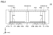
- FIG. 2 is a side perspective view of the LC filter 100.
- the LC filter 100 includes a rectangular parallelepiped or substantially rectangular parallelepiped laminated body 110 in which a plurality of dielectric layers are laminated in the stacking direction. Each dielectric layer of the laminate 110 is formed of, for example, ceramic. Inside the laminate 110, the inductor and the capacitor are composed of a plurality of wiring patterns and electrodes provided in each dielectric layer, and a plurality of vias provided between the dielectric layers. These inductors and capacitors form an LC resonant circuit.
- the stacking direction of the laminated body 110 is defined as the "Z-axis direction", and the direction perpendicular to the Z-axis direction and along the long side of the laminated body 110 is defined as the "X-axis direction” of the laminated body 110.
- the direction along the short side is defined as the "Y-axis direction”.
- the positive direction of the Z axis in each figure may be referred to as an upper side, and the negative direction may be referred to as a lower side.
- the dielectric of the laminated body 110 is omitted, and only the wiring pattern, vias, and conductors of the terminals formed inside are shown. ..
- FIG. 2 is a side perspective view of the LC filter 100 as viewed from the negative direction of the Y axis of FIG. 1.
- the laminate 110 has an upper surface 111 and a lower surface 112.
- An input terminal T1, an output terminal T2, and a ground terminal GND are provided on the lower surface 112 of the laminated body 110.
- the input terminal T1, the output terminal T2, and the ground terminal GND are external terminals for connecting the LC filter 100 and an external device, and are flat plate-shaped electrodes.
- the input terminal T1, the output terminal T2, and the ground terminal GND are LGA (Land Grid Array) terminals regularly arranged on the lower surface 112 of the laminated body 110.
- the flat plate electrode PG2 is provided on the dielectric layer close to the lower surface 112 of the laminated body 110. As shown in FIG. 2, the flat plate electrode PG2 is connected to the ground terminal GND via the via VGA and VGB. Further, the flat plate electrode PG1 is provided on the dielectric layer close to the upper surface 111 of the laminated body 110. In FIG. 1, the flat plate electrode PG1 is shown by a broken line.
- the flat plate electrode PG1 and the flat plate electrode PG2 are connected by ground vias VG11, VG12, and VG13 extending in the stacking direction of the laminated body 110.
- the ground vias VG11 and VG13 are arranged along the side surface 113 (first side surface) in the positive direction of the Y axis of the laminated body 110.
- the ground via VG11 is located in the negative corner of the X-axis and the ground via VG13 is located in the positive corner of the X-axis.
- the ground via VG12 is arranged along the negative side surface 114 (second side surface) of the laminated body 110 near the center in the X-axis direction.
- the side surface 113 and the side surface 114 face each other.
- a plurality of flat plate-shaped electrodes P11 to P15 are provided on the dielectric layer between the flat plate electrode PG1 and the flat plate electrode PG2. These plurality of electrodes P11 to P15 are arranged apart from the flat plate electrode PG2, and form a capacitor with the flat plate electrode PG2.
- the electrodes P11 to P15 are also referred to as “capacitor electrodes”.
- the capacitor electrodes P11 to P15 are arranged apart from each other and are capacitively coupled to each other.
- Inductor vias V11 to V15 constituting the LC resonance circuit are connected to the capacitor electrodes P11 to P15, respectively.
- the input terminal T1 is connected to the capacitor electrode P11 via the via V11A and the wiring electrode P11A.
- One end of the inductor via V11 is connected to the capacitor electrode P11, and the other end is connected to the wiring electrode PA1.
- the wiring electrode PA1 is provided in the dielectric layer between the flat plate electrode PG1 and the capacitor electrode P11, and connects the inductor via V11 and the ground via VG11. That is, the other end of the inductor via V11 is connected to the position between the flat plate electrode PG1 and the flat plate electrode PG2 in the ground via VG11 by the wiring electrode PA1.
- the inductor via V11 and the capacitor electrode P11 form an LC resonant circuit (first resonant circuit RC1) directly connected to the ground via VG11.
- the output terminal T2 is connected to the capacitor electrode P15 via the via V15A and the wiring electrode P15A.
- One end of the inductor via V15 is connected to the capacitor electrode P15, and the other end is connected to the wiring electrode PA2.
- the wiring electrode PA2 is provided in the dielectric layer between the flat plate electrode PG1 and the capacitor electrode P15, and connects the inductor via V15 and the ground via VG13. That is, the other end of the inductor via V15 is connected to the position between the flat plate electrode PG1 and the flat plate electrode PG2 in the ground via VG13 by the wiring electrode PA2. With such a configuration, the inductor via V15 and the capacitor electrode P15 form an LC resonant circuit (fifth resonant circuit RC5) directly connected to the ground via VG13.
- the inductor via V12 is arranged in the negative corner of the X-axis along the side surface 114.
- the inductor via V12 is connected to the flat plate electrode PG1 and the capacitor electrode P12, and constitutes an LC resonance circuit (second resonance circuit RC2).
- the inductor via V13 is arranged near the center of the X-axis along the side surface 113. That is, the inductor via V13 is arranged between the ground via VG11 and the ground via VG13 along the side surface 113.
- the inductor via V13 is connected to the flat plate electrode PG1 and the capacitor electrode P13, and constitutes an LC resonance circuit (third resonance circuit RC3).
- the inductor via V14 is arranged in the positive corner of the X-axis along the side surface 114.
- the inductor via V14 is connected to the flat plate electrode PG1 and the capacitor electrode P14, and constitutes an LC resonance circuit (fourth resonance circuit RC4).
- the LC filter 100 has a configuration in which a plurality of resonant circuits are adjacent to each other, and functions as a bandpass filter by the attenuation pole generated by the magnetic coupling and / or the capacitive coupling of the adjacent resonant circuits.
- the high frequency signal supplied to the input terminal T1 is output from the output terminal T2 via the first resonance circuit RC1, the second resonance circuit RC2, the third resonance circuit RC3, the fourth resonance circuit RC4, and the fifth resonance circuit RC5. Will be done.
- FIG. 3 is a plan view for explaining a signal (current) transmission path in the plate electrode PG1 of the LC filter 100 of FIG.
- the high frequency signal supplied to the input terminal T1 is transmitted from the first resonant circuit RC1 to the adjacent second resonant circuit RC2 by magnetic coupling, as shown by the arrow AR0.
- the signal transmitted to the second resonance circuit RC2 is transmitted to the adjacent third resonance circuit RC3 through the flat plate electrode PG1 as shown by the arrow AR1, and further adjacent to the third resonance circuit RC3 as shown by the arrow AR2. It is transmitted to the fourth resonant circuit RC4 (arrow AR2).
- the signal transmitted to the fourth resonant circuit RC4 is transmitted to the fifth resonant circuit RC5 by magnetic coupling as shown by the arrow AR3, and is output from the output terminal T2.
- the first resonance circuit RC1 and the fifth resonance which are resonance circuits connected to the input / output terminals, are used so that the degree of coupling between the resonance circuits does not become too high.
- the circuit RC5 is configured to be connected to the ground vias VG11 and VG13 by the wiring electrodes PA1 and PA2. More specifically, as shown in FIG. 1 and the like, the inductor vias V11 and V15 in the first resonant circuit RC1 and the fifth resonant circuit RC5 are not directly connected to the flat plate electrode PG1 unlike the other resonant circuits.
- the ground vias VG11 and VG13 are connected to the flat plate electrodes PG1 and PG2 via the wiring electrodes PA1 and PA2, respectively.
- the Q value of the resonant circuit arranged in the middle stage greatly contributes to the Q value of the entire filter device, and the Q of the resonant circuit near the end (input / output terminal). It is known that the value has a relatively small effect on the Q value of the entire filter. Therefore, as described above, by making the resonance circuit connected to the input / output terminal a circuit connected to the ground via, the degree of coupling between the resonance circuits does not become too high while maintaining the Q value of the entire filter. Can be done.
- the inductor vias V12, V13, V14 in the flat plate electrode PG1 Grand vias VG11, VG12, and VG13 are arranged on both sides of the signal transmission path (arrows AR1 and AR2) between them.
- the virtual line CL1 (first virtual line) connecting the inductor via V12 and the inductor via V13 and the virtual line CL2 (second virtual line) connecting the ground via VG11 and the ground via VG12 intersect.
- the virtual line CL3 connecting the inductor via V13 and the inductor via V14 and the virtual line CL4 connecting the ground via VG12 and the ground via VG13 intersect.
- Inductor vias so that the virtual line CL1 and the virtual line CL2 intersect each other at the midpoint, and the virtual line CL3 and the virtual line CL4 intersect each other at the midpoint in order to realize the symmetry of the characteristics in the filter. And it is preferable to arrange the ground vias symmetrically.
- the “plate electrode PG1" and “plate electrode PG2" in the first embodiment correspond to the “first electrode” and the “second electrode” in the present disclosure, respectively.
- the “grand vias VG11 to VG13” in the first embodiment correspond to the "first grand via” to the “third ground via” in the present disclosure, respectively, and comprehensively correspond to the "connection electrode” in the present disclosure.
- the “capacitor electrode P11”, “capacitor electrode P12”, “capacitor electrode P13”, “capacitor electrode P15”, and “capacitor electrode P14” in the first embodiment are the “first capacitor electrode” to the "fifth capacitor” in the present disclosure. Corresponds to each of the electrodes.
- the “inductor via V11”, “inductor via V12”, “inductor via V13”, “inductor via V15”, and “inductor via V14" in the first embodiment are the “first inductor via” to "fifth inductor” in the present disclosure. Corresponds to “via” respectively.
- FIG. 4 is a perspective perspective view of the LC filter 100 # of the comparative example.
- the first resonance circuit RC1 connected to the input terminal T1 and the fifth resonance circuit RC5 connected to the output terminal T2 are each first. It has a configuration that replaces the resonance circuit RC1 # and the fifth resonance circuit RC5 #.
- the wiring electrode PA1 in the first embodiment is deleted.
- the inductor via V11 # is connected to the flat plate electrode PG1 and the capacitor electrode P11.
- the wiring electrode PA2 in the first embodiment is deleted, and the inductor via V15 # is connected to the flat plate electrode PG1 and the capacitor electrode P15. That is, the first resonance circuit RC1 # and the fifth resonance circuit RC5 # are configured to be directly connected to the flat plate electrode PG1.
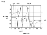
- FIG. 5 is a diagram for explaining the passing characteristics of the LC filter 100 of the first embodiment and the LC filter 100 # in the comparative example.
- the horizontal axis shows the frequency
- the vertical axis shows the insertion loss from the input terminal T1 to the output terminal T2.
- the solid lines LN10 and LN10A show the case of the LC filter 100 of the first embodiment
- the broken lines LN11 and LN11A show the case of the LC filter 100 # of the comparative example.
- the solid line LN10A and the broken line LN11A are magnified vertical axes of the solid line LN10 and the broken line LN11 (scale on the right axis).
- the specification of the pass band of the LC filter is 4400 MHz to 5000 MHz.
- the LC filter 100 of the first embodiment is the LC filter 100 of the comparative example.
- the insertion loss is larger than that of #. This is because, in the first embodiment, the degree of coupling is reduced by the configuration in which the first resonance circuit RC1 and the fifth resonance circuit RC5 are directly connected to the ground via as described above. There is. However, with respect to the frequency bandwidth in which the insertion loss is 3 dB or less, almost the same bandwidth can be realized in both cases.
- the attenuation is about 25 dB in the comparative example, whereas the attenuation up to about 60 dB can be realized in the first embodiment. Further, on the high frequency side of the pass band, although the amount of attenuation is almost the same, the first embodiment can realize steeper attenuation.
- the resonance circuit connected to the input / output terminal is directly connected to the ground via, so that the increase of the filter loss in the pass band is suppressed. , The attenuation characteristic in the non-passband can be improved.
- Modification example In the first embodiment, an example of the configuration of an LC filter having a five-stage resonant circuit has been described. In the following modification examples 1 to 3, an example of an LC filter having resonance circuits having different numbers of stages will be described.
- FIG. 6 is a plan view of the LC filter 100A of Modification 1.
- the LC filter 100A has a four-stage resonant circuit. More specifically, the LC filter 100A includes a first resonant circuit RC1A including an inductor via V21 and a wiring electrode PA21, a second resonant circuit RC2A including an inductor via V22, and a third resonant circuit RC3A including an inductor via V23. , A fourth resonant circuit RC4A including an inductor via V24 and a wiring electrode PA22.
- a capacitor electrode is connected to each inductor via as in the LC filter 100 of the first embodiment.
- the inductor vias V22 and V23 are arranged at one diagonal corner of the flat plate electrode PG1 on the rectangle. Further, the ground vias VG21 and VG22 are arranged at the other diagonal corners of the flat plate electrode PG1. In other words, the ground via VG21 and the inductor via V23 are arranged along the side surface 113 of the laminate 110. Further, the ground via VG22 and the inductor via V22 are arranged along the side surface 114 of the laminated body 110.
- the inductor vias V22, V23 and the ground vias VG21 and VG22 are arranged so that the virtual line connecting the inductor vias V22 and V23 and the virtual line connecting the ground vias VG21 and VG22 intersect.
- the inductor via V21 is arranged between the ground via VG21 and the inductor via V22.
- One end of the inductor via V21 is connected to an input terminal via a capacitor electrode.
- the other end of the inductor via V21 is connected to an intermediate position (position between the flat plate electrode PG1 and the flat plate electrode PG2) of the ground via VG21 via the wiring electrode PA21. That is, the first resonant circuit RC1A has a configuration in which it is directly connected to the ground via.
- the inductor via V24 is arranged between the ground via VG22 and the inductor via V23. One end of the inductor via V24 is connected to the output terminal via a capacitor electrode. Further, the other end of the inductor via V24 is connected to an intermediate position (position between the flat plate electrode PG1 and the flat plate electrode PG2) of the ground via VG22 via the wiring electrode PA22. That is, the fourth resonant circuit RC4A has a configuration in which it is directly connected to the ground via.
- the high frequency signal supplied to the input terminal is transmitted from the first resonance circuit RC1A to the second resonance circuit RC2A by magnetic coupling as shown by the arrow AR20.
- the signal transmitted to the second resonance circuit RC2A is transmitted to the third resonance circuit RC3A through the plate electrode PG1 as shown by the arrow AR21, and further, as shown by the arrow AR22, the fourth resonance by magnetic coupling. It is transmitted to the circuit RC4A and output from the output terminal.
- the LC filter 100A has a configuration in which the first resonant circuit RC1A connected to the input terminal and the fourth resonant circuit RC4A connected to the output terminal are directly connected to the ground via. Further, ground vias VG21 and VG22 are arranged on both sides of the signal (current) transmission path from the second resonance circuit RC2A to the third resonance circuit RC3A in the flat plate electrode PG1. With such a configuration, also in the LC filter 100A of the first modification, the degree of coupling between the resonance circuits is reduced while suppressing the decrease in the Q value of the entire filter as in the first embodiment. .. Therefore, it is possible to improve the attenuation characteristics while suppressing the decrease in the insertion loss of the filter.
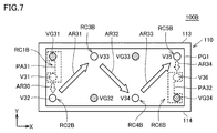
- FIG. 7 is a plan view of the LC filter 100B of the modification 2.
- the LC filter 100B has a configuration including a six-stage resonant circuit in which another one-stage resonant circuit is added to the configuration of the LC filter 100 of the first embodiment.
- the LC filter 100B includes a first resonant circuit RC1B including an inductor via V31 and a wiring electrode PA31, a second resonant circuit RC2B including an inductor via V32, and a third resonant circuit RC3B including an inductor via V33.
- a capacitor electrode is connected to each inductor via.
- the ground vias VG31 and VG33 and the inductor vias V33 and V35 are located along the side surface 113 of the laminate 110 in the positive direction of the X-axis, and the ground vias VG31 and the inductor vias V33.
- the ground via VG33 and the inductor via V35 are arranged in this order.
- ground vias VG32 and VG34 and the inductor vias V32 and V34 are arranged in the order of the inductor vias V32, the ground vias VG32, the inductor vias V34, and the ground vias VG34 in the positive direction of the X axis along the side surface 114 of the laminated body 110. Has been done.
- the first resonant circuit RC1B has a configuration in which it is directly connected to the intermediate position of the ground via VG31 by the wiring electrode PA31. Further, the sixth resonant circuit RC6B is configured to be directly connected to the intermediate position of the ground via VG34 by the wiring electrode PA32.
- the high frequency signals supplied to the input terminals are the first resonance circuit RC1B, the second resonance circuit RC2B, the third resonance circuit RC3B, the fourth resonance circuit RC4B, and the fifth resonance.
- the circuit RC5B and the sixth resonant circuit RC6B are transmitted in this order and output from the output terminal.
- the ground vias VG31 to VG34 are arranged on both sides of the signal transmission path (arrows AR31 to AR33) in the plate electrode PG1.
- the LC filter 100B has a configuration in which the first resonant circuit RC1B connected to the input terminal and the sixth resonant circuit RC6B connected to the output terminal are directly connected to the ground via. Further, in the flat plate electrode PG1, ground vias are arranged on both sides of the signal transmission path between adjacent resonance circuits. With such a configuration, even in the LC filter 100B of the second modification, the degree of coupling between the resonance circuits is reduced while suppressing the decrease in the Q value of the entire filter. Therefore, it is possible to improve the attenuation characteristics while suppressing the decrease in the insertion loss of the filter.
- the "grand vias VG31 to VG33" in the second modification correspond to the "first grand vias” to the “third grand vias” in the present disclosure, respectively.
- the “Grand Via VG31 to VG34” in the second modification comprehensively correspond to the "connection electrode” in the present disclosure.
- the "inductor via V31”, “inductor via V32”, “inductor via V33”, “inductor via V36”, and “inductor via V34" in the second modification are the “first inductor via” to "fifth inductor via” in the present disclosure. Corresponds to each.
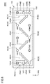
- FIG. 8 is a plan view of the LC filter 100C of the modification 3.
- the LC filter 100C has a configuration including a seven-stage resonant circuit in which another one-stage resonant circuit is added to the configuration of the LC filter 100B of the second modification.
- the LC filter 100C includes a first resonant circuit RC1C including an inductor via V41 and a wiring electrode PA41, a second resonant circuit RC2C including an inductor via V42, and a third resonant circuit RC3C including an inductor via V43.
- a capacitor electrode is connected to each inductor via.
- the ground vias VG41, VG43, VG45 and the inductor vias V43, V45 are in the positive direction of the X axis along the side surface 113 of the laminate 110, and the ground vias VG41 and the inductor vias.
- V43, ground via VG43, inductor via V45, and ground via VG45 are arranged in this order.
- the ground vias VG42, VG44 and the inductor vias V42, V44, V46 have the inductor vias V42, the ground vias VG42, the inductor vias V44, the ground vias VG44, and The inductor vias V46 are arranged in this order.
- the first resonant circuit RC1C has a configuration in which it is directly connected to the intermediate position of the ground via VG41 by the wiring electrode PA41. Further, the seventh resonant circuit RC7C has a configuration in which the wiring electrode PA42 is directly connected to the intermediate position of the ground via VG45.
- the high frequency signal supplied to the input terminal is the first resonance circuit RC1C, the second resonance circuit RC2C, the third resonance circuit RC3C, the fourth resonance circuit RC4C, and the fifth resonance.
- the circuit RC5C, the sixth resonant circuit RC6C, and the seventh resonant circuit RC7C are transmitted in this order and output from the output terminal.
- the ground vias VG41 to VG45 are arranged on both sides of the signal transmission path (arrows AR41 to AR44) in the plate electrode PG1.
- the LC filter 100C has a configuration in which the first resonant circuit RC1C connected to the input terminal and the seventh resonant circuit RC7C connected to the output terminal are directly connected to the ground via. Further, in the flat plate electrode PG1, ground vias are arranged on both sides of the signal transmission path between adjacent resonance circuits. With such a configuration, even in the LC filter 100C of the modified example 3, the degree of coupling between the resonance circuits is reduced while suppressing the decrease in the Q value of the entire filter. Therefore, it is possible to improve the attenuation characteristics while suppressing the decrease in the insertion loss of the filter.
- the "grand vias VG41 to VG43" in the modified example 3 correspond to the "first grand vias” to the “third grand vias” in the present disclosure, respectively.
- the “Grand Via VG41 to VG45” in the third modification comprehensively correspond to the "connection electrode” in the present disclosure.
- the "inductor via V41”, “inductor via V42”, “inductor via V46”, and “inductor via V47” in the third modification correspond to the "first inductor via” to the "fourth inductor via” in the present disclosure, respectively.
- FIG. 9 is a perspective perspective view of the LC filter 100D according to the second embodiment.
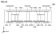
- FIG. 10 is a side perspective view of the LC filter 100D when viewed from the side surface 114 of the laminated body 110.
- the LC filter 100D has a configuration including a four-stage resonance circuit as in the modification 1 in the first embodiment described above.
- the LC filter 100D includes flat plate electrodes PG1 and PG2 provided on the laminated body 110, input terminals T1 and output terminals T2, inductor vias V51 to V54, and ground vias VG51 to VG54.
- the capacitor electrodes P51 to P54 and the wiring electrodes PA51 and PA52 are provided.
- the flat plate electrode PG1 is provided on the dielectric layer close to the upper surface 111 of the laminated body 110, and the flat plate electrode PG2 is provided on the dielectric layer close to the lower surface 112.
- the flat plate electrode PG2 is connected to the ground terminal GND provided on the lower surface 112 via the via VGA and VGB.
- the ground vias VG51 to VG54 are arranged at the four corners of the laminated body 110 when the laminated body 110 is viewed in a plan view from the laminated body direction (Z-axis direction). Specifically, the ground vias VG51 and VG53 are arranged in the order of the ground vias VG51 and the ground vias VG53 along the side surface 113 of the laminated body 110 in the X-axis direction. Further, the ground vias VG52 and VG54 are arranged in the order of the ground vias VG52 and the ground vias VG54 along the side surface 114 of the laminated body 110 in the X-axis direction. Each of the ground vias VG51 to VG54 connects the flat plate electrode PG1 and the flat plate electrode PG2.
- the dielectric layer between the flat plate electrode PG1 and the flat plate electrode PG2 is provided with flat plate-shaped capacitor electrodes P51 to P54.
- the capacitor electrodes P51 to P54 are arranged apart from the flat plate electrode PG2 and form a capacitor with the flat plate electrode PG2.
- the capacitor electrodes P52 and P53 are arranged apart from each other along the Y-axis near the center in the X-axis direction when the laminated body 110 is viewed in a plan view from the stacking direction.
- Inductor vias V52 and V53 having one end connected to the flat plate electrode PG1 are connected to the capacitor electrodes P52 and P53, respectively.
- the inductor via V52 is arranged between the ground via VG52 and the ground via VG54 along the side surface 114 of the laminated body 110.
- the inductor via V53 is arranged between the ground via VG51 and the ground via VG53 along the side surface 113 of the laminated body 110.
- An LC resonance circuit (second resonance circuit RC2D) is configured by the inductor via V52 and the capacitor electrode P52.
- An LC resonance circuit (third resonance circuit RC3D) is configured by the inductor via V53 and the capacitor electrode P53.
- the capacitor electrodes P51 and P54 are arranged apart from each other along the X-axis near the center in the Y-axis direction when the laminated body 110 is viewed in a plan view from the stacking direction. A part of the capacitor electrodes P52 and P53 is arranged between the capacitor electrode P51 and the capacitor electrode P54.
- the capacitor electrode P51 is connected to the input terminal T1 provided on the lower surface 112 of the laminated body 110 via the via V51A. Further, one end of the inductor via V51 is connected to the capacitor electrode P51. The other end of the inductor via V51 is connected to the wiring electrode PA51.
- the wiring electrode PA51 is provided on the dielectric layer between the flat plate electrode PG1 and the flat plate electrode PG2.
- the inductor via V51 is connected to an intermediate position (a position between the flat plate electrode PG1 and the flat plate electrode PG2) of the ground via VG51 by the wiring electrode PA51.
- the inductor via V51, the wiring electrode PA51, and the capacitor electrode P51 constitute an LC resonant circuit (first resonant circuit RC1D) directly connected to the ground via.
- the capacitor electrode P54 is connected to the output terminal T2 provided on the lower surface 112 of the laminated body 110 via the via V54A. Further, one end of the inductor via V54 is connected to the capacitor electrode P54. The other end of the inductor via V54 is connected to the wiring electrode PA52.
- the wiring electrode PA52 is provided on the dielectric layer between the flat plate electrode PG1 and the flat plate electrode PG2.
- the inductor via V54 is connected to the intermediate position (position between the flat plate electrode PG1 and the flat plate electrode PG2) of the ground via VG53 by the wiring electrode PA52.
- the inductor via V54, the wiring electrode PA52, and the capacitor electrode P54 constitute an LC resonant circuit (fourth resonant circuit RC4D) directly connected to the ground via.
- the LC filter 100D has a configuration in which a plurality of resonant circuits are adjacent to each other, and functions as a bandpass filter by the attenuation pole generated by the magnetic coupling and / or the capacitive coupling of the adjacent resonant circuits.
- the high frequency signal supplied to the input terminal T1 is output from the output terminal T2 via the first resonance circuit RC1D, the second resonance circuit RC2D, the third resonance circuit RC3D, and the fourth resonance circuit RC4D.
- the LC filter 100D has a configuration in which the first resonance circuit RC1D and the fourth resonance circuit RC4D connected to the input / output terminals are directly connected to the ground via in a plurality of stages of resonance circuits. Further, in the flat plate electrode PG1, the virtual line connecting the inductor via V52 and the inductor via V53 intersects with the virtual line connecting the ground via VG51 and the ground via VG54 or the virtual line connecting the ground via VG52 and the ground via VG53. doing. With such a configuration, as described in the first embodiment, the degree of coupling between the resonance circuits is reduced while suppressing the decrease in the Q value of the entire filter. Therefore, it is possible to improve the attenuation characteristics while suppressing the decrease in the insertion loss of the filter.
- the "grand vias VG51 to VG54" in the second embodiment correspond to the "first grand via", the “second grand via”, the “fifth grand via”, and the “sixth grand via” in the present disclosure, respectively. Comprehensively corresponds to the "connection electrode” in the present disclosure.
- the “capacitor electrodes P51 to P54” in the second embodiment correspond to the “first capacitor electrode” to the “fourth capacitor electrode” in the present disclosure, respectively.
- the “inductor vias V51 to V54” in the second embodiment correspond to the "first inductor via” to the "fourth inductor via” in the present disclosure, respectively.
- FIG. 11 is a perspective perspective view of the LC filter 100E according to the third embodiment.
- the flat plate electrode PG1 and the flat plate electrode PG2 are connected by a flat plate-shaped electrode provided on the side surface of the laminated body 110 instead of the ground via in the LC filter 100D of the second embodiment.
- the description of the element overlapping with the LC filter 100D of FIG. 10 is not repeated.
- a flat plate-shaped side electrode PGA is provided on the side surface 113 of the laminated body, and a flat plate-shaped side electrode PGB is provided on the side surface 114.
- the end faces of the flat plate electrodes PG1 and PG2 are connected to the side electrode PGA and PGB.
- the inductor via V51 connected to the input terminal T1 is connected to the side electrode PGA by the wiring electrode PA51A. Further, the inductor via V54 connected to the output terminal T2 is connected to the side electrode PGA by the wiring electrode PA52A.
- Each of the wiring electrodes PA51A and PA52A is provided in a dielectric layer between the flat plate electrode PG1 and the flat plate electrode PG2, and is connected at a position between the flat plate electrode PG1 and the flat plate electrode PG2 of the side electrode PGA.
- the inductor via V51, the capacitor electrode P51, and the wiring electrode PA51A form an LC resonant circuit (first resonant circuit RC1E) directly connected to the ground via.
- the inductor via V54, the capacitor electrode P54, and the wiring electrode PA54A constitute an LC resonant circuit (fourth resonant circuit RC4E) directly connected to the ground via.
- the wiring electrodes PA51A and PA52A may be connected to the side electrode PGB instead of the side electrode PGA.
- the high frequency signal supplied to the input terminal T1 is the first resonant circuit RC1E, the second resonant circuit RC2E formed by the inductor via V52 and the capacitor electrode P52, and the third resonant circuit RC3E formed by the inductor via V53 and the capacitor electrode P53. , And is transmitted via the fourth resonant circuit RC4E and output from the output terminal T2.
- the first resonant circuit RC1E connected to the input / output terminals and The fourth resonant circuit RC4E is configured to be directly connected to the ground via. Therefore, even in the LC filter 100E, the degree of coupling between the resonance circuits is reduced while suppressing the decrease in the Q value of the entire filter, so that the attenuation characteristics are improved while suppressing the decrease in the insertion loss of the filter. Can be done.
- the "side electrode PGA, PGB" in the third embodiment comprehensively corresponds to the "connection electrode” in the present disclosure.
Landscapes
- Engineering & Computer Science (AREA)
- Power Engineering (AREA)
- Manufacturing & Machinery (AREA)
- Microelectronics & Electronic Packaging (AREA)
- Filters And Equalizers (AREA)
- Coils Or Transformers For Communication (AREA)
Abstract
LCフィルタ(100)は、入力端子(T1)と、出力端子(T2)と、積層体(110)と、平板電極(PG1,PG2)と、平板電極を接続する接続電極(VG11~VG13)と、複数のキャパシタ電極と、複数のインダクタビアとを備える。各キャパシタ電極は、平板電極(PG2)と対向している。インダクタビア(V11)の一方端はキャパシタ電極(P1)を介して入力端子(T1)に接続される。インダクタビア(V11)の他方端は接続電極(VG11)の中間に接続される。インダクタビア(V12)は、平板電極(PG1)とキャパシタ電極(P12)との間に接続される。インダクタビア(V14)は、平板電極(PG1)とキャパシタ電極(P14)との間に接続される。インダクタビア(V15)の一方端はキャパシタ電極(P15)を介して出力端子(T2)に接続される。インダクタビア(V15)の他方端は接続電極(VG13)の中間に接続される。
Description
本開示はLCフィルタに関し、より特定的には、積層LCフィルタにおける特性を改善するための技術に関する。
特開2000-165171号公報(特許文献1)には、インダクタおよびキャパシタにより構成された複数段の共振器が多層基板内に形成されたLCフィルタが開示されている。特開2000-165171号公報(特許文献1)に開示されたLCフィルタにおいては、各段の共振器が、隣接する他の共振器と磁気結合および/または容量結合することによって、所望のフィルタ特性を実現している。
上記のようなLCフィルタは、携帯電話あるいはスマートフォンに代表される携帯用の通信機器に用いられる場合がある。このような携帯端末においては、小型化および薄型化のニーズが依然として高く、それに伴って内部に搭載される電子部品についても小型化が求められている。
特開2000-165171号公報(特許文献1)に開示されたような複数段の共振器を有するLCフィルタにおいては、共振器の段数を増加することによって、非通過帯域における減衰特性を改善することができることが知られている。しかしながら、積層体内に形成される共振器の数が増加すると、共振器同士の結合が強まってしまい、フィルタの損失は低下するものの、かえって非通過帯域の信号が十分に減衰できない状態となる可能性がある。
本開示は、このような課題を解決するためになされたものであって、その目的は、多段型の積層LCフィルタにおいて、フィルタ損失の増加を抑制しつつ、減衰特性を向上させることである。
本開示に係るLCフィルタは、入力端子と、出力端子と、複数の誘電体層を含む積層体と、第1電極および第2電極と、第1電極と第2電極とを接続する接続電極と、第1キャパシタ電極、第2キャパシタ電極、第3キャパシタ電極および第4キャパシタ電極と、第1インダクタビア、第2インダクタビア、第3インダクタビアおよび第4インダクタビアとを備える。第1電極および第2電極は、積層体において、互いに異なる誘電体層に設けられている。第1キャパシタ電極、第2キャパシタ電極、第3キャパシタ電極および第4キャパシタ電極は、第2電極と対向している。第1キャパシタ電極は第1インダクタビアに接続されている。第2キャパシタ電極は第2インダクタビアに接続されている。第3キャパシタ電極は第3インダクタビアに接続されている。第4キャパシタ電極は第4インダクタビアに接続されている。第1インダクタビアの一方端は、第1キャパシタ電極を介して入力端子に接続される。第1インダクタビアの他方端は、接続電極における第1電極と第2電極との間の位置に接続される。第2インダクタビアは、第1電極と第2キャパシタ電極との間に接続される。第3インダクタビアは、第1電極と第3キャパシタ電極との間に接続される。第4インダクタビアの一方端は、第4キャパシタ電極を介して出力端子に接続される。第4インダクタビアの他方端は、接続電極における第1電極と第2電極との間の位置に接続される。
本開示によるLCフィルタによれば、フィルタを構成する多段構成の共振回路のうち、入出力端子に接続される共振回路が、第1電極と第2電極とを接続する接続電極に直接接続される。これによって、入出力端子に接続される共振回路による磁気結合が弱まる。したがって、フィルタの損失の増加を抑制しつつ、減衰特性を向上させることができる。
以下、本開示の実施の形態について、図面を参照しながら詳細に説明する。なお、図中同一または相当部分には同一符号を付してその説明は繰り返さない。
[実施の形態1]
(フィルタの構成)
まず、図1および図2を用いて、実施の形態1に従うLCフィルタ100の構成について説明する。図1はLCフィルタ100の斜視透視図である。また、図2は、LCフィルタ100の側面透視図である。LCフィルタ100は、複数の誘電体層が積層方向に積層された、直方体または略直方体の積層体110を備えている。積層体110の各誘電体層は、たとえばセラミックにより形成されている。積層体110の内部において、各誘電体層に設けられた複数の配線パターンおよび電極、ならびに誘電体層間に設けられた複数のビアによってインダクタおよびキャパシタが構成されている。これらのインダクタおよびキャパシタにより、LC共振回路が構成される。
(フィルタの構成)
まず、図1および図2を用いて、実施の形態1に従うLCフィルタ100の構成について説明する。図1はLCフィルタ100の斜視透視図である。また、図2は、LCフィルタ100の側面透視図である。LCフィルタ100は、複数の誘電体層が積層方向に積層された、直方体または略直方体の積層体110を備えている。積層体110の各誘電体層は、たとえばセラミックにより形成されている。積層体110の内部において、各誘電体層に設けられた複数の配線パターンおよび電極、ならびに誘電体層間に設けられた複数のビアによってインダクタおよびキャパシタが構成されている。これらのインダクタおよびキャパシタにより、LC共振回路が構成される。
以下の説明においては、積層体110の積層方向を「Z軸方向」とし、Z軸方向に垂直であって積層体110の長辺に沿った方向を「X軸方向」とし、積層体110の短辺に沿った方向を「Y軸方向」とする。また、以下では、各図におけるZ軸の正方向を上側、負方向を下側と称する場合がある。
なお、図1および後述する図4,図9,図11においては、積層体110の誘電体は省略してあり、内部に形成される配線パターン、ビアおよび端子の導電体のみが示されている。
図2は、図1のY軸の負方向からLCフィルタ100を見た、LCフィルタ100の側面透視図である。図1および図2を参照して、積層体110は、上面111および下面112を有する。積層体110の下面112に、入力端子T1、出力端子T2および接地端子GNDが設けられている。入力端子T1、出力端子T2および接地端子GNDは、LCフィルタ100と外部機器とを接続するための外部端子であり、平板状の電極である。具体的には、入力端子T1、出力端子T2および接地端子GNDは、積層体110の下面112に規則的に配置されたLGA(Land Grid Array)端子である。
積層体110の下面112に近接した誘電体層に、平板電極PG2が設けられている。図2に示されるように、平板電極PG2はビアVGA,VGBを介して接地端子GNDに接続されている。また、積層体110の上面111に近接した誘電体層に、平板電極PG1が設けられている。なお、図1においては、平板電極PG1は破線で示されている。
平板電極PG1および平板電極PG2は、積層体110の積層方向に延在するグランドビアVG11、VG12,VG13によって接続されている。グランドビアVG11,VG13は、積層体110のY軸の正方向の側面113(第1側面)に沿って配置されている。グランドビアVG11はX軸の負方向の隅に配置され、グランドビアVG13はX軸の正方向の隅に配置されている。グランドビアVG12は、積層体110の負方向の側面114(第2側面)に沿って、X軸方向のほぼ中央付近に配置されている。側面113と側面114とは互いに対向している。
平板電極PG1と平板電極PG2との間の誘電体層には、複数の平板状の電極P11~P15が設けられている。これらの複数の電極P11~P15は、平板電極PG2から離間して配置されており、平板電極PG2との間でキャパシタを構成する。以下、電極P11~P15を「キャパシタ電極」とも称する。キャパシタ電極P11~P15は、互いに離間して配置されており、互いに容量結合している。キャパシタ電極P11~P15には、LC共振回路を構成するインダクタビアV11~V15がそれぞれ接続されている。
入力端子T1は、ビアV11Aおよび配線電極P11Aを介して、キャパシタ電極P11に接続されている。インダクタビアV11は、一方端がキャパシタ電極P11に接続されており、他方端が配線電極PA1に接続されている。配線電極PA1は、平板電極PG1とキャパシタ電極P11との間の誘電体層に設けられており、インダクタビアV11とグランドビアVG11とを接続している。すなわち、インダクタビアV11の他方端は、配線電極PA1によって、グランドビアVG11における平板電極PG1と平板電極PG2との間の位置に接続されている。このような構成によって、インダクタビアV11およびキャパシタ電極P11は、グランドビアVG11に直接接続されたLC共振回路(第1共振回路RC1)を構成する。
出力端子T2は、ビアV15Aおよび配線電極P15Aを介して、キャパシタ電極P15に接続されている。インダクタビアV15は、一方端がキャパシタ電極P15に接続されており、他方端が配線電極PA2に接続されている。配線電極PA2は、平板電極PG1とキャパシタ電極P15との間の誘電体層に設けられており、インダクタビアV15とグランドビアVG13とを接続している。すなわち、インダクタビアV15の他方端は、配線電極PA2によって、グランドビアVG13における平板電極PG1と平板電極PG2との間の位置に接続されている。このような構成によって、インダクタビアV15およびキャパシタ電極P15は、グランドビアVG13に直接接続されたLC共振回路(第5共振回路RC5)を構成する。
インダクタビアV12は、側面114に沿って、X軸の負方向の隅に配置されている。インダクタビアV12は、平板電極PG1およびキャパシタ電極P12に接続されており、LC共振回路(第2共振回路RC2)を構成する。
インダクタビアV13は、側面113に沿って、X軸の中央付近に配置されている。すなわち、インダクタビアV13は、側面113に沿って、グランドビアVG11とグランドビアVG13との間に配置されている。インダクタビアV13は、平板電極PG1およびキャパシタ電極P13に接続されており、LC共振回路(第3共振回路RC3)を構成する。
インダクタビアV14は、側面114に沿って、X軸の正方向の隅に配置されている。インダクタビアV14は、平板電極PG1およびキャパシタ電極P14に接続されており、LC共振回路(第4共振回路RC4)を構成する。
このように、LCフィルタ100は、複数の共振回路が隣接した構成を有しており、隣接する共振回路同士が磁気結合および/または容量結合することによって生じる減衰極によりバンドパスフィルタとして機能する。入力端子T1に供給された高周波信号は、第1共振回路RC1、第2共振回路RC2、第3共振回路RC3、第4共振回路RC4および第5共振回路RC5を経由して、出力端子T2から出力される。
図3は、図1のLCフィルタ100の平板電極PG1における信号(電流)の伝達経路を説明するための平面図である。図3を参照して、入力端子T1に供給された高周波信号は、矢印AR0で示すように、第1共振回路RC1から、磁気結合によって、隣接する第2共振回路RC2へ伝達される。第2共振回路RC2に伝達された信号は、矢印AR1で示すように、平板電極PG1を通して隣接する第3共振回路RC3へ伝達され、さらに、矢印AR2で示すように、第3共振回路RC3に隣接する第4共振回路RC4へと伝達される(矢印AR2)。そして、第4共振回路RC4に伝達された信号は、矢印AR3で示すように、第5共振回路RC5に磁気結合により伝達されて、出力端子T2から出力される。
ここで、各共振回路間において信号を伝達する場合、所望の通過帯域の信号の損失を低減させる観点からは、共振回路間の結合度を高くしてQ値を高めることが重要である。一方で、フィルタ装置の場合、非通過帯域の信号はできるだけ伝達されないようにすることが好ましい。すなわち、非通過帯域の信号を減衰させる観点からは、共振回路間の結合度を低減することも必要となる。
そこで、実施の形態1のLCフィルタ100においては、共振回路間の結合度が高くなり過ぎないようにするために、入出力端子に接続される共振回路である第1共振回路RC1,第5共振回路RC5が、配線電極PA1,PA2によってグランドビアVG11,VG13に接続されている構成としている。より詳細には、図1等に示されるように、第1共振回路RC1および第5共振回路RC5におけるインダクタビアV11,V15は、他の共振回路のように平板電極PG1に直接接続されておらず、配線電極PA1,PA2をそれぞれ介して、グランドビアVG11,VG13により平板電極PG1,PG2に接続されている。このような構成とすることによって、第1共振回路RC1と第2共振回路RC2との間の結合度、および、第4共振回路RC4と第5共振回路RC5との間の結合度を、第1共振回路RC1および第5共振回路RC5が平板電極PG1に直接接続される場合に比べて低減することができる。
なお、一般的に、多段型のLCフィルタにおいては、中段部に配置された共振回路のQ値がフィルタ装置全体のQ値に大きく寄与し、端部(入出力端子)に近い共振回路のQ値はフィルタ全体のQ値への影響が比較的小さいことが知られている。そのため、上記のように、入出力端子に接続された共振回路がグランドビアに接続された回路とすることで、フィルタ全体のQ値を維持しつつ、共振回路間の結合度が高くなり過ぎないようにすることができる。
また、実施の形態1のLCフィルタ100においては、図3に示されるように、積層体110を積層方向(Z軸方向)から平面視した場合に、平板電極PG1におけるインダクタビアV12,V13,V14間の信号伝達経路(矢印AR1,AR2)の両側にグランドビアVG11,VG12,VG13が配置されている。具体的には、インダクタビアV12とインダクタビアV13とを結ぶ仮想線CL1(第1仮想線)と、グランドビアVG11とグランドビアVG12とを結ぶ仮想線CL2(第2仮想線)とが交差している。同様に、インダクタビアV13とインダクタビアV14とを結ぶ仮想線CL3と、グランドビアVG12とグランドビアVG13とを結ぶ仮想線CL4とが交差している。
なお、フィルタにおける特性の対称性を実現するために、仮想線CL1と仮想線CL2とが互いに中点で交差し、仮想線CL3と仮想線CL4とが互いに中点で交差するように、インダクタビアおよびグランドビアを対称的に配置することが好ましい。
このようなビアの配置によって、平板電極PG1上において、インダクタビアV12からインダクタビアV13へ伝達される信号(電流)の一部が、矢印AR1A,矢印AR1BのようにグランドビアVG11,VG12へと漏洩する。同様に、インダクタビアV13からインダクタビアV14へ伝達される信号(電流)の一部が、矢印AR2A,矢印AR2BのようにグランドビアVG12,VG13へと漏洩する。これによって、第2共振回路RC2と第3共振回路RC3との間の結合度、および、第3共振回路RC3と第4共振回路RC4との間の結合度が若干低減される。
なお、実施の形態1における「平板電極PG1」および「平板電極PG2」は、本開示における「第1電極」および「第2電極」にそれぞれ対応する。実施の形態1における「グランドビアVG11~VG13」は、本開示における「第1グランドビア」~「第3グランドビア」にそれぞれ対応し、包括的に本開示における「接続電極」に対応する。実施の形態1における「キャパシタ電極P11」,「キャパシタ電極P12」,「キャパシタ電極P13」,「キャパシタ電極P15」,「キャパシタ電極P14」は、本開示における「第1キャパシタ電極」~「第5キャパシタ電極」にそれぞれ対応する。実施の形態1における「インダクタビアV11」,「インダクタビアV12」,「インダクタビアV13」,「インダクタビアV15」,「インダクタビアV14」は、本開示における「第1インダクタビア」~「第5インダクタビア」にそれぞれ対応する。
(フィルタ特性)
次に、実施の形態1のLCフィルタ100の通過特性を、比較例の場合と比較しつつ説明する。
次に、実施の形態1のLCフィルタ100の通過特性を、比較例の場合と比較しつつ説明する。
図4は、比較例のLCフィルタ100#の斜視透視図である。比較例のLCフィルタ100#においては、実施の形態1のLCフィルタ100において、入力端子T1に接続された第1共振回路RC1および出力端子T2に接続された第5共振回路RC5が、それぞれ第1共振回路RC1#および第5共振回路RC5#に置き換わった構成となっている。
具体的には、比較例における第1共振回路RC1#においては、実施の形態1における配線電極PA1が削除されている。そして、インダクタビアV11#は、平板電極PG1およびキャパシタ電極P11に接続されている。同様に、第5共振回路RC5#においては、実施の形態1における配線電極PA2が削除されており、インダクタビアV15#は、平板電極PG1およびキャパシタ電極P15に接続されている。すなわち、第1共振回路RC1#および第5共振回路RC5#は、平板電極PG1に直接接続された構成となっている。
図5は、実施の形態1のLCフィルタ100、および比較例におけるLCフィルタ100#の通過特性を説明するための図である。図5においては、横軸には周波数が示されており、縦軸には入力端子T1から出力端子T2への挿入損失が示されている。図5において、実線LN10、LN10Aは実施の形態1のLCフィルタ100の場合を示しており、破線LN11、LN11Aは比較例のLCフィルタ100#の場合を示している。なお、実線LN10Aおよび破線LN11Aは、実線LN10および破線LN11の縦軸を拡大したものである(右軸目盛)。なお、当該LCフィルタの通過帯域の仕様は4400MHz~5000MHzである。
図5を参照して、通過帯域における挿入損失については、実線LN10Aおよび破線LN11Aに示されるように、ピーク値で見ると、実施の形態1のLCフィルタ100の方が、比較例のLCフィルタ100#に比べて挿入損失が大きくなっている。これは、実施の形態1においては、上述のように第1共振回路RC1および第5共振回路RC5がグランドビアに直接接続された構成とすることによって結合度が減少していることに起因している。ただし、挿入損失が3dB以下となる周波数帯域幅については、両者ともほぼ同程度の帯域幅が実現できている。
減衰特性については、通過帯域よりも低周波数側については、比較例では約25dBの減衰であるのに対し、実施の形態1では約60dBまでの減衰が実現できている。また、通過帯域よりも高周波数側については、減衰量についてはほぼ同程度ではあるが、実施の形態1の方がより急峻な減衰を実現できている。
このように、実施の形態1のLCフィルタ100においては、入出力端子に接続される共振回路がグランドビアに直接接続された構成とすることによって、通過帯域におけるフィルタの損失の増加を抑制しつつ、非通過帯域における減衰特性を向上させることができる。
(変形例)
実施の形態1においては、5段の共振回路を有するLCフィルタの構成の例について説明した。以下の変形例1~3においては、異なる段数の共振回路を有するLCフィルタの例について説明する。
実施の形態1においては、5段の共振回路を有するLCフィルタの構成の例について説明した。以下の変形例1~3においては、異なる段数の共振回路を有するLCフィルタの例について説明する。
(a)変形例1
図6は、変形例1のLCフィルタ100Aの平面図である。LCフィルタ100Aは、4段の共振回路を有している。より具体的には、LCフィルタ100Aは、インダクタビアV21および配線電極PA21を含む第1共振回路RC1Aと、インダクタビアV22を含む第2共振回路RC2Aと、インダクタビアV23を含む第3共振回路RC3Aと、インダクタビアV24および配線電極PA22を含む第4共振回路RC4Aとを備えている。なお、図6には図示されていないが、各インダクタビアには、実施の形態1のLCフィルタ100と同様に、キャパシタ電極が接続されている。
図6は、変形例1のLCフィルタ100Aの平面図である。LCフィルタ100Aは、4段の共振回路を有している。より具体的には、LCフィルタ100Aは、インダクタビアV21および配線電極PA21を含む第1共振回路RC1Aと、インダクタビアV22を含む第2共振回路RC2Aと、インダクタビアV23を含む第3共振回路RC3Aと、インダクタビアV24および配線電極PA22を含む第4共振回路RC4Aとを備えている。なお、図6には図示されていないが、各インダクタビアには、実施の形態1のLCフィルタ100と同様に、キャパシタ電極が接続されている。
積層体110を積層方向から平面視した場合に、インダクタビアV22,V23は矩形上の平板電極PG1の一方の対角線の隅に配置されている。また、グランドビアVG21、VG22は、平板電極PG1の他方の対角線の隅に配置されている。言い換えれば、グランドビアVG21およびインダクタビアV23は、積層体110の側面113に沿って配置されている。また、グランドビアVG22およびインダクタビアV22は、積層体110の側面114に沿って配置されている。インダクタビアV22,V23を結ぶ仮想線と、グランドビアVG21、VG22を結ぶ仮想線とが交差するように、インダクタビアV22,V23およびグランドビアVG21、VG22が配置されている。
インダクタビアV21は、グランドビアVG21とインダクタビアV22との間に配置されている。インダクタビアV21の一方端は、キャパシタ電極を介して入力端子に接続されている。また、インダクタビアV21の他方端は、配線電極PA21を介して、グランドビアVG21の中間位置(平板電極PG1と平板電極PG2との間の位置)に接続されている。すなわち、第1共振回路RC1Aはグランドビアに直接接続された構成となっている。
インダクタビアV24は、グランドビアVG22とインダクタビアV23との間に配置されている。インダクタビアV24の一方端は、キャパシタ電極を介して出力端子に接続されている。また、インダクタビアV24の他方端は、配線電極PA22を介して、グランドビアVG22の中間位置(平板電極PG1と平板電極PG2との間の位置)に接続されている。すなわち、第4共振回路RC4Aはグランドビアに直接接続された構成となっている。
入力端子に供給された高周波信号は、矢印AR20で示すように、磁気結合により、第1共振回路RC1Aから第2共振回路RC2Aに伝達される。第2共振回路RC2Aに伝達された信号は、矢印AR21で示すように、平板電極PG1を通って第3共振回路RC3Aへと伝達され、さらに、矢印AR22で示すように、磁気結合により第4共振回路RC4Aに伝達されて、出力端子から出力される。
LCフィルタ100Aにおいては、入力端子に接続される第1共振回路RC1A、および、出力端子に接続される第4共振回路RC4Aがグランドビアに直接接続された構成となっている。さらに、平板電極PG1における第2共振回路RC2Aから第3共振回路RC3Aへの信号(電流)の伝達経路の両側に、グランドビアVG21,VG22が配置されている。このような構成とすることによって、変形例1のLCフィルタ100Aにおいても、実施の形態1と同様に、フィルタ全体のQ値の低下を抑制しながら、各共振回路間の結合度が低減される。したがって、フィルタの挿入損失の低下を抑制しつつ、減衰特性を向上させることができる。
なお、変形例1における「グランドビアVG21,VG22」は、本開示における「第1グランドビア」および「第2グランドビア」にそれぞれ対応し、包括的に本開示における「接続電極」に対応する。変形例1における「インダクタビアV21~V24」は、本開示における「第1インダクタビア」~「第4インダクタビア」にそれぞれ対応する。
(b)変形例2
図7は、変形例2のLCフィルタ100Bの平面図である。LCフィルタ100Bは、実施の形態1のLCフィルタ100の構成にさらにもう1段共振回路を追加した、6段の共振回路を含む構成を有している。
図7は、変形例2のLCフィルタ100Bの平面図である。LCフィルタ100Bは、実施の形態1のLCフィルタ100の構成にさらにもう1段共振回路を追加した、6段の共振回路を含む構成を有している。
より具体的には、LCフィルタ100Bは、インダクタビアV31および配線電極PA31を含む第1共振回路RC1Bと、インダクタビアV32を含む第2共振回路RC2Bと、インダクタビアV33を含む第3共振回路RC3Bと、インダクタビアV34を含む第4共振回路RC4Bと、インダクタビアV35を含む第5共振回路RC5Bと、インダクタビアV36および配線電極PA32を含む第6共振回路RC6Bとを備えている。なお、図7には図示されていないが、各インダクタビアには、キャパシタ電極が接続されている。
積層体110を積層方向から平面視した場合に、グランドビアVG31,VG33およびインダクタビアV33,V35は、積層体110の側面113に沿ってX軸の正方向に、グランドビアVG31、インダクタビアV33、グランドビアVG33、およびインダクタビアV35の順に配置されている。また、グランドビアVG32,VG34およびインダクタビアV32,V34は、積層体110の側面114に沿ってX軸の正方向に、インダクタビアV32、グランドビアVG32、インダクタビアV34、およびグランドビアVG34の順に配置されている。
第1共振回路RC1Bは、配線電極PA31によってグランドビアVG31の中間位置に直接接続された構成となっている。また、第6共振回路RC6Bは、配線電極PA32によってグランドビアVG34の中間位置に直接接続された構成となっている。
入力端子に供給された高周波信号は、図7における矢印AR30~AR34で示されるように、第1共振回路RC1B、第2共振回路RC2B、第3共振回路RC3B、第4共振回路RC4B、第5共振回路RC5Bおよび第6共振回路RC6Bの順に伝達されて、出力端子から出力される。グランドビアVG31~VG34は、平板電極PG1における信号の伝達経路(矢印AR31~AR33)の両側に配置されている。
LCフィルタ100Bにおいては、入力端子に接続される第1共振回路RC1B、および、出力端子に接続される第6共振回路RC6Bがグランドビアに直接接続された構成となっている。さらに、平板電極PG1において、隣接する共振回路間の信号伝達経路の両側にグランドビアが配置されている。このような構成とすることによって、変形例2のLCフィルタ100Bにおいても、フィルタ全体のQ値の低下を抑制しながら、各共振回路間の結合度が低減される。したがって、フィルタの挿入損失の低下を抑制しつつ、減衰特性を向上させることができる。
なお、変形例2における「グランドビアVG31~VG33」は、本開示における「第1グランドビア」~「第3グランドビア」にそれぞれ対応する。変形例2における「グランドビアVG31~VG34」は、包括的に本開示における「接続電極」に対応する。変形例2における「インダクタビアV31」,「インダクタビアV32」,「インダクタビアV33」,「インダクタビアV36」,「インダクタビアV34」は、本開示における「第1インダクタビア」~「第5インダクタビア」にそれぞれ対応する。
(c)変形例3
図8は、変形例3のLCフィルタ100Cの平面図である。LCフィルタ100Cは、変形例2のLCフィルタ100Bの構成にさらにもう1段共振回路を追加した、7段の共振回路を含む構成を有している。
図8は、変形例3のLCフィルタ100Cの平面図である。LCフィルタ100Cは、変形例2のLCフィルタ100Bの構成にさらにもう1段共振回路を追加した、7段の共振回路を含む構成を有している。
より具体的には、LCフィルタ100Cは、インダクタビアV41および配線電極PA41を含む第1共振回路RC1Cと、インダクタビアV42を含む第2共振回路RC2Cと、インダクタビアV43を含む第3共振回路RC3Cと、インダクタビアV44を含む第4共振回路RC4Cと、インダクタビアV45を含む第5共振回路RC5Cと、インダクタビアV46を含む第6共振回路RC6Cと、インダクタビアV47および配線電極PA42を含む第7共振回路RC7Cとを備えている。なお、図8には図示されていないが、各インダクタビアには、キャパシタ電極が接続されている。
積層体110を積層方向から平面視した場合に、グランドビアVG41,VG43,VG45およびインダクタビアV43,V45は、積層体110の側面113に沿ってX軸の正方向に、グランドビアVG41、インダクタビアV43、グランドビアVG43、インダクタビアV45、およびグランドビアVG45の順に配置されている。また、グランドビアVG42,VG44およびインダクタビアV42,V44,V46は、積層体110の側面114に沿ってX軸の正方向に、インダクタビアV42、グランドビアVG42、インダクタビアV44、グランドビアVG44、およびインダクタビアV46の順に配置されている。
第1共振回路RC1Cは、配線電極PA41によってグランドビアVG41の中間位置に直接接続された構成となっている。また、第7共振回路RC7Cは、配線電極PA42によってグランドビアVG45の中間位置に直接接続された構成となっている。
入力端子に供給された高周波信号は、図8における矢印AR40~AR45で示されるように、第1共振回路RC1C、第2共振回路RC2C、第3共振回路RC3C、第4共振回路RC4C、第5共振回路RC5C、第6共振回路RC6C、および第7共振回路RC7Cの順に伝達されて、出力端子から出力される。グランドビアVG41~VG45は、平板電極PG1における信号の伝達経路(矢印AR41~AR44)の両側に配置されている。
LCフィルタ100Cにおいては、入力端子に接続される第1共振回路RC1C、および、出力端子に接続される第7共振回路RC7Cがグランドビアに直接接続された構成となっている。さらに、平板電極PG1において、隣接する共振回路間の信号伝達経路の両側にグランドビアが配置されている。このような構成とすることによって、変形例3のLCフィルタ100Cにおいても、フィルタ全体のQ値の低下を抑制しながら、各共振回路間の結合度が低減される。したがって、フィルタの挿入損失の低下を抑制しつつ、減衰特性を向上させることができる。
なお、変形例3における「グランドビアVG41~VG43」は、本開示における「第1グランドビア」~「第3グランドビア」にそれぞれ対応する。変形例3における「グランドビアVG41~VG45」は、包括的に本開示における「接続電極」に対応する。変形例3における「インダクタビアV41」,「インダクタビアV42」,「インダクタビアV46」,「インダクタビアV47」は、本開示における「第1インダクタビア」~「第4インダクタビア」にそれぞれ対応する。
上記の実施の形態1および変形例においては、4段~7段の共振回路を有するLCフィルタの例について説明したが、さらに多くの段数を有するLCフィルタにおいても同様の構成を適用することができる。
[実施の形態2]
実施の形態2においては、インダクタビアおよびグランドビアを異なる配置としたLCフィルタの構成の例について説明する。
実施の形態2においては、インダクタビアおよびグランドビアを異なる配置としたLCフィルタの構成の例について説明する。
図9は、実施の形態2に従うLCフィルタ100Dの斜視透視図である。また、図10は、LCフィルタ100Dにおいて、積層体110の側面114から見たときの側面透視図である。LCフィルタ100Dは、上述の実施の形態1における変形例1と同様に、4段の共振回路を備えた構成を有している。
図9および図10を参照して、LCフィルタ100Dは、積層体110に設けられた平板電極PG1,PG2と、入力端子T1および出力端子T2と、インダクタビアV51~V54と、グランドビアVG51~VG54と、キャパシタ電極P51~P54と、配線電極PA51,PA52とを備える。
実施の形態1のLCフィルタ100と同様に、積層体110の上面111に近接した誘電体層に平板電極PG1が設けられ、下面112に近接した誘電体層に平板電極PG2が設けられている。平板電極PG2は、ビアVGA,VGBを介して下面112に設けられた接地端子GNDに接続されている。
グランドビアVG51~VG54は、積層体110を積層方向(Z軸方向)から平面視した場合に、積層体110の四隅にそれぞれ配置されている。具体的には、グランドビアVG51,VG53は、積層体110の側面113に沿ってX軸方向に、グランドビアVG51およびグランドビアVG53の順に配置されている。また、グランドビアVG52,VG54は、積層体110の側面114に沿ってX軸方向に、グランドビアVG52およびグランドビアVG54の順に配置されている。グランドビアVG51~VG54の各々は、平板電極PG1と平板電極PG2とを接続している。
平板電極PG1と平板電極PG2との間の誘電体層には、平板状のキャパシタ電極P51~P54が設けられている。キャパシタ電極P51~P54は、平板電極PG2から離間して配置されており、平板電極PG2との間でキャパシタを形成する。
キャパシタ電極P52,P53は、積層体110を積層方向から平面視した場合に、X軸方向の中央付近にY軸に沿って互いに離間して配置されている。キャパシタ電極P52,P53には、一方端が平板電極PG1に接続されたインダクタビアV52,V53がそれぞれ接続されている。インダクタビアV52は、積層体110の側面114に沿って、グランドビアVG52とグランドビアVG54との間に配置されている。インダクタビアV53は、積層体110の側面113に沿って、グランドビアVG51とグランドビアVG53との間に配置されている。インダクタビアV52およびキャパシタ電極P52によって、LC共振回路(第2共振回路RC2D)が構成される。インダクタビアV53およびキャパシタ電極P53によって、LC共振回路(第3共振回路RC3D)が構成される。
キャパシタ電極P51,P54は、積層体110を積層方向から平面視した場合に、Y軸方向の中央付近にX軸に沿って互いに離間して配置されている。キャパシタ電極P51とキャパシタ電極P54との間に、キャパシタ電極P52,P53の一部が配置されている。
キャパシタ電極P51は、ビアV51Aを介して、積層体110の下面112に設けられた入力端子T1に接続される。また、キャパシタ電極P51には、インダクタビアV51の一方端が接続される。インダクタビアV51の他方端は、配線電極PA51に接続されている。配線電極PA51は、平板電極PG1と平板電極PG2との間の誘電体層に設けられている。インダクタビアV51は、配線電極PA51によって、グランドビアVG51の中間位置(平板電極PG1と平板電極PG2との間の位置)に接続される。インダクタビアV51、配線電極PA51およびキャパシタ電極P51によって、グランドビアに直接接続されたLC共振回路(第1共振回路RC1D)が構成される。
キャパシタ電極P54は、ビアV54Aを介して、積層体110の下面112に設けられた出力端子T2に接続される。また、キャパシタ電極P54には、インダクタビアV54の一方端が接続される。インダクタビアV54の他方端は、配線電極PA52に接続されている。配線電極PA52は、平板電極PG1と平板電極PG2との間の誘電体層に設けられている。インダクタビアV54は、配線電極PA52によって、グランドビアVG53の中間位置(平板電極PG1と平板電極PG2との間の位置)に接続される。インダクタビアV54、配線電極PA52およびキャパシタ電極P54によって、グランドビアに直接接続されたLC共振回路(第4共振回路RC4D)が構成される。
このように、LCフィルタ100Dは、複数の共振回路が隣接した構成を有しており、隣接する共振回路同士が磁気結合および/または容量結合することによって生じる減衰極によりバンドパスフィルタとして機能する。入力端子T1に供給された高周波信号は、第1共振回路RC1D、第2共振回路RC2D、第3共振回路RC3D、および第4共振回路RC4Dを経由して、出力端子T2から出力される。
LCフィルタ100Dにおいては、複数段の共振回路において、入出力端子に接続される第1共振回路RC1Dおよび第4共振回路RC4Dが、グランドビアに直接接続された構成となっている。さらに、平板電極PG1において、インダクタビアV52とインダクタビアV53とを結ぶ仮想線が、グランドビアVG51とグランドビアVG54とを結ぶ仮想線、あるいは、グランドビアVG52とグランドビアVG53とを結ぶ仮想線と交差している。このような構成によって、実施の形態1で説明したように、フィルタ全体のQ値の低下を抑制しながら、各共振回路間の結合度が低減される。したがって、フィルタの挿入損失の低下を抑制しつつ、減衰特性を向上させることができる。
なお、実施の形態2における「グランドビアVG51~VG54」は、本開示における「第1グランドビア」,「第2グランドビア」,「第5グランドビア」,「第6グランドビア」にそれぞれ対応し、包括的に本開示における「接続電極」に対応する。実施の形態2における「キャパシタ電極P51~P54」は、本開示における「第1キャパシタ電極」~「第4キャパシタ電極」にそれぞれ対応する。実施の形態2における「インダクタビアV51~V54」は、本開示における「第1インダクタビア」~「第4インダクタビア」にそれぞれ対応する。
[実施の形態3]
実施の形態3においては、平板電極PG1と平板電極PG2との接続の他の構成例について説明する。
実施の形態3においては、平板電極PG1と平板電極PG2との接続の他の構成例について説明する。
図11は、実施の形態3に従うLCフィルタ100Eの斜視透視図である。LCフィルタ100Eにおいては、実施の形態2のLCフィルタ100Dにおけるグランドビアに代えて、積層体110の側面に設けられた平板状の電極によって、平板電極PG1および平板電極PG2が接続される。なお、図11において、図10のLCフィルタ100Dと重複する要素の説明は繰り返さない。
図11を参照して、LCフィルタ100Eにおいては、積層体の側面113に平板状の側面電極PGAが設けられており、側面114に平板状の側面電極PGBが設けられている。側面電極PGA,PGBには、平板電極PG1,PG2の端面が接続されている。
そして、入力端子T1に接続されるインダクタビアV51は、配線電極PA51Aによって、側面電極PGAに接続されている。また、出力端子T2に接続されるインダクタビアV54は、配線電極PA52Aによって、側面電極PGAに接続されている。配線電極PA51A,PA52Aの各々は、平板電極PG1と平板電極PG2との間の誘電体層に設けられており、側面電極PGAの平板電極PG1と平板電極PG2との間の位置において接続される。これにより、インダクタビアV51、キャパシタ電極P51および配線電極PA51Aによって、グランドビアに直接接続されたLC共振回路(第1共振回路RC1E)が構成される。また、インダクタビアV54、キャパシタ電極P54および配線電極PA54Aによって、グランドビアに直接接続されたLC共振回路(第4共振回路RC4E)が構成される。なお、配線電極PA51A,PA52Aの一方あるいは双方が、側面電極PGAに代えて側面電極PGBに接続される構成であってもよい。
入力端子T1に供給された高周波信号は、第1共振回路RC1E、インダクタビアV52およびキャパシタ電極P52で形成される第2共振回路RC2E、インダクタビアV53およびキャパシタ電極P53で形成される第3共振回路RC3E、および第4共振回路RC4Eを経由して伝達され、出力端子T2から出力される。
このように、グランドビアに代えて、側面電極PGA,PGBによって平板電極PG1,PG2が接続された構成を有する多段型のLCフィルタ100Eにおいては、入出力端子に接続される第1共振回路RC1Eおよび第4共振回路RC4Eがグランドビアに直接接続された構成とされている。そのため、LCフィルタ100Eにおいても、フィルタ全体のQ値の低下を抑制しながら、各共振回路間の結合度が低減されるので、フィルタの挿入損失の低下を抑制しつつ、減衰特性を向上させることができる。
実施の形態3における「側面電極PGA,PGB」は、包括的に本開示における「接続電極」に対応する。
今回開示された実施の形態は、すべての点で例示であって制限的なものではないと考えられるべきである。本開示の範囲は、上記した実施の形態の説明ではなくて請求の範囲によって示され、請求の範囲と均等の意味および範囲内でのすべての変更が含まれることが意図される。
100,100A~100E フィルタ、110 積層体、111 上面、112 下面、113,114 側面、GND 接地端子、P11~P15,P51~P54 キャパシタ電極、P11A,P15A,PA1,PA2,PA21,PA22,PA31,PA32,PA41,PA42,PA51,PA51A,PA52,PA52A,PA54A 配線電極、PG1,PG2 平板電極、PGA,PGB 側面電極、RC1,RC1A~RC1E,RC1#,RC2,RC2A~RC2E,RC3,RC3A~RC3E,RC4,RC4A~RC4E,RC5,RC5B,RC5C,RC5#,RC6B,RC6C,RC7C 共振回路、T1 入力端子、T2 出力端子、V11~V15,V21~V24,V31~V36,V41~V47,V51~V54,V11#,V15# インダクタビア、V11A,V15A,V51A,V54A,VGA,VGB ビア、VG11~VG13,VG21,VG22,VG31~VG34,VG41~VG45,VG51~VG54 グランドビア。
Claims (10)
- 入力端子と、
出力端子と、
複数の誘電体層を含む積層体と、
前記積層体において、互いに異なる誘電体層に設けられた第1電極および第2電極と、
前記第1電極と前記第2電極とを接続する接続電極と、
前記第2電極と対向する第1キャパシタ電極、第2キャパシタ電極、第3キャパシタ電極および第4キャパシタ電極と、
前記第1キャパシタ電極に接続された第1インダクタビアと、
前記第2キャパシタ電極に接続された第2インダクタビアと、
前記第3キャパシタ電極に接続された第3インダクタビアと、
前記第4キャパシタ電極に接続された第4インダクタビアとを備え、
前記第1インダクタビアの一方端は前記第1キャパシタ電極を介して前記入力端子に接続され、
前記第1インダクタビアの他方端は前記接続電極における前記第1電極と前記第2電極との間の位置に接続され、
前記第2インダクタビアは、前記第1電極と前記第2キャパシタ電極との間に接続され、
前記第3インダクタビアは、前記第1電極と前記第3キャパシタ電極との間に接続され、
前記第4インダクタビアの一方端は前記第4キャパシタ電極を介して前記出力端子に接続され、
前記第4インダクタビアの他方端は前記接続電極における前記第1電極と前記第2電極との間の位置に接続される、LCフィルタ。 - 接地端子をさらに備え、
前記第1電極および前記第2電極は、前記接地端子に接続されており、
前記積層体は、互いに対向する第1側面および第2側面を有する直方体に設けられており、
前記接続電極は、前記積層体の積層方向に延在する第1グランドビアおよび第2グランドビアを含み、
前記積層体の積層方向から平面視した場合に、
前記第1グランドビアおよび前記第3インダクタビアは、前記第1側面に沿って配置され、
前記第2グランドビアおよび前記第2インダクタビアは、前記第2側面に沿って配置される、請求項1に記載のLCフィルタ。 - 前記積層体の積層方向から平面視した場合に、前記第2インダクタビアと前記第3インダクタビアとを結ぶ第1仮想線と、前記第1グランドビアと前記第2グランドビアとを結ぶ第2仮想線とが交差する、請求項2に記載のLCフィルタ。
- 前記第2仮想線は、前記第1仮想線の中点において前記第1仮想線と交差する、請求項3に記載のLCフィルタ。
- 前記第2仮想線は、前記第2仮想線の中点において前記第1仮想線と交差する、請求項4に記載のLCフィルタ。
- 前記第2電極と対向する第5キャパシタ電極と、
前記第2側面に沿って配置され、前記第1電極および前記第5キャパシタ電極に接続された第5インダクタビアとをさらに備え、
前記積層体の積層方向から平面視した場合に、
前記接続電極は、前記第1側面に沿って配置され、前記第1電極と前記第2電極とを接続する第3グランドビアをさらに含み、
前記第2グランドビアは、前記第2インダクタビアと前記第5インダクタビアとの間に配置され、
前記第3インダクタビアは、前記第1グランドビアと前記第3グランドビアとの間に配置される、請求項2~5のいずれか1項に記載のLCフィルタ。 - 前記第1電極と前記第2電極とを接続する第5グランドビアおよび第6グランドビアをさらに備え、
前記積層体の積層方向から平面視した場合に、
前記第3インダクタビアは、前記第1側面に沿って、前記第1グランドビアと前記第5グランドビアとの間に配置され、
前記第2インダクタビアは、前記第2側面に沿って、前記第2グランドビアと前記第6グランドビアとの間に配置される、請求項2に記載のLCフィルタ。 - 前記積層体は、互いに対向する第1側面および第2側面を有する直方体であり、
前記接続電極は、前記第1側面および前記第2側面に設けられた平板状の電極である、請求項1に記載のLCフィルタ。 - 前記積層体は、セラミックで形成される、請求項1~8のいずれか1項に記載のLCフィルタ。
- 前記LCフィルタは、バンドパスフィルタである、請求項1~9のいずれか1項に記載のLCフィルタ。
Priority Applications (3)
| Application Number | Priority Date | Filing Date | Title |
|---|---|---|---|
| JP2022527655A JP7424483B2 (ja) | 2020-05-25 | 2021-05-11 | Lcフィルタ |
| CN202180032092.XA CN115461991B (zh) | 2020-05-25 | 2021-05-11 | Lc滤波器 |
| US17/970,648 US12191835B2 (en) | 2020-05-25 | 2022-10-21 | LC filter |
Applications Claiming Priority (2)
| Application Number | Priority Date | Filing Date | Title |
|---|---|---|---|
| JP2020090711 | 2020-05-25 | ||
| JP2020-090711 | 2020-05-25 |
Related Child Applications (1)
| Application Number | Title | Priority Date | Filing Date |
|---|---|---|---|
| US17/970,648 Continuation US12191835B2 (en) | 2020-05-25 | 2022-10-21 | LC filter |
Publications (1)
| Publication Number | Publication Date |
|---|---|
| WO2021241208A1 true WO2021241208A1 (ja) | 2021-12-02 |
Family
ID=78723384
Family Applications (1)
| Application Number | Title | Priority Date | Filing Date |
|---|---|---|---|
| PCT/JP2021/017900 Ceased WO2021241208A1 (ja) | 2020-05-25 | 2021-05-11 | Lcフィルタ |
Country Status (4)
| Country | Link |
|---|---|
| US (1) | US12191835B2 (ja) |
| JP (1) | JP7424483B2 (ja) |
| CN (1) | CN115461991B (ja) |
| WO (1) | WO2021241208A1 (ja) |
Cited By (2)
| Publication number | Priority date | Publication date | Assignee | Title |
|---|---|---|---|---|
| WO2023139901A1 (ja) * | 2022-01-19 | 2023-07-27 | 株式会社村田製作所 | フィルタ装置 |
| JP2024049210A (ja) * | 2022-09-28 | 2024-04-09 | Tdk株式会社 | 積層型電子部品 |
Families Citing this family (1)
| Publication number | Priority date | Publication date | Assignee | Title |
|---|---|---|---|---|
| JP7786409B2 (ja) * | 2023-02-17 | 2025-12-16 | 株式会社村田製作所 | フィルタ装置 |
Citations (5)
| Publication number | Priority date | Publication date | Assignee | Title |
|---|---|---|---|---|
| WO2007119356A1 (ja) * | 2006-04-14 | 2007-10-25 | Murata Manufacturing Co., Ltd. | 積層帯域通過フィルタ |
| WO2010018798A1 (ja) * | 2008-08-11 | 2010-02-18 | 日立金属株式会社 | バンドパスフィルタ、高周波部品及び通信装置 |
| JP2014027690A (ja) * | 2013-10-22 | 2014-02-06 | Murata Mfg Co Ltd | 帯域通過フィルタ |
| WO2018100923A1 (ja) * | 2016-12-02 | 2018-06-07 | 株式会社村田製作所 | Lc共振器およびlcフィルタ |
| JP2019012977A (ja) * | 2017-07-03 | 2019-01-24 | Tdk株式会社 | 積層型電子部品 |
Family Cites Families (11)
| Publication number | Priority date | Publication date | Assignee | Title |
|---|---|---|---|---|
| JP2000165171A (ja) | 1998-11-30 | 2000-06-16 | Murata Mfg Co Ltd | Lc共振器部品及びlcフィルタ |
| TWI268659B (en) * | 2005-07-15 | 2006-12-11 | Delta Electronics Inc | Dual-band bandpass filter |
| US7671706B2 (en) | 2006-04-14 | 2010-03-02 | Murata Manufacturing Co., Ltd | High frequency multilayer bandpass filter |
| US8106722B2 (en) | 2008-08-20 | 2012-01-31 | Panasonic Corporation | Multi-layered device and electronic equipment using thereof |
| JP2013128232A (ja) * | 2011-12-19 | 2013-06-27 | Murata Mfg Co Ltd | バンドパスフィルタ |
| JP6428917B2 (ja) * | 2015-03-25 | 2018-11-28 | 株式会社村田製作所 | ダイプレクサ |
| JP6547707B2 (ja) * | 2016-07-29 | 2019-07-24 | 株式会社村田製作所 | 積層フィルタ |
| CN109906553B (zh) * | 2016-11-07 | 2023-06-06 | 株式会社村田制作所 | 层叠型lc滤波器 |
| TWI656731B (zh) * | 2016-12-04 | 2019-04-11 | 日商村田製作所股份有限公司 | Multilayer LC filter |
| CN113939999B (zh) * | 2019-07-09 | 2025-09-09 | 株式会社村田制作所 | Lc滤波器 |
| CN210609090U (zh) * | 2019-11-25 | 2020-05-22 | 中国计量大学上虞高等研究院有限公司 | 一种小型化高抑制ltcc柱型电感带通滤波器 |
-
2021
- 2021-05-11 CN CN202180032092.XA patent/CN115461991B/zh active Active
- 2021-05-11 WO PCT/JP2021/017900 patent/WO2021241208A1/ja not_active Ceased
- 2021-05-11 JP JP2022527655A patent/JP7424483B2/ja active Active
-
2022
- 2022-10-21 US US17/970,648 patent/US12191835B2/en active Active
Patent Citations (5)
| Publication number | Priority date | Publication date | Assignee | Title |
|---|---|---|---|---|
| WO2007119356A1 (ja) * | 2006-04-14 | 2007-10-25 | Murata Manufacturing Co., Ltd. | 積層帯域通過フィルタ |
| WO2010018798A1 (ja) * | 2008-08-11 | 2010-02-18 | 日立金属株式会社 | バンドパスフィルタ、高周波部品及び通信装置 |
| JP2014027690A (ja) * | 2013-10-22 | 2014-02-06 | Murata Mfg Co Ltd | 帯域通過フィルタ |
| WO2018100923A1 (ja) * | 2016-12-02 | 2018-06-07 | 株式会社村田製作所 | Lc共振器およびlcフィルタ |
| JP2019012977A (ja) * | 2017-07-03 | 2019-01-24 | Tdk株式会社 | 積層型電子部品 |
Cited By (5)
| Publication number | Priority date | Publication date | Assignee | Title |
|---|---|---|---|---|
| WO2023139901A1 (ja) * | 2022-01-19 | 2023-07-27 | 株式会社村田製作所 | フィルタ装置 |
| JPWO2023139901A1 (ja) * | 2022-01-19 | 2023-07-27 | ||
| JP7666657B2 (ja) | 2022-01-19 | 2025-04-22 | 株式会社村田製作所 | フィルタ装置 |
| JP2024049210A (ja) * | 2022-09-28 | 2024-04-09 | Tdk株式会社 | 積層型電子部品 |
| JP7807351B2 (ja) | 2022-09-28 | 2026-01-27 | Tdk株式会社 | 積層型電子部品 |
Also Published As
| Publication number | Publication date |
|---|---|
| CN115461991B (zh) | 2025-12-12 |
| US12191835B2 (en) | 2025-01-07 |
| JPWO2021241208A1 (ja) | 2021-12-02 |
| JP7424483B2 (ja) | 2024-01-30 |
| US20230044859A1 (en) | 2023-02-09 |
| CN115461991A (zh) | 2022-12-09 |
Similar Documents
| Publication | Publication Date | Title |
|---|---|---|
| JP7424482B2 (ja) | Lcフィルタ | |
| US10944375B2 (en) | Multilayer band pass filter | |
| JP7424483B2 (ja) | Lcフィルタ | |
| CN106410357B (zh) | 定向耦合器 | |
| CN107666298B (zh) | 层叠滤波器 | |
| CN105830343A (zh) | 滤波元器件 | |
| US20220294410A1 (en) | Band-pass filter | |
| WO2022097492A1 (ja) | フィルタ装置およびそれを搭載した高周波フロントエンド回路 | |
| WO2021111761A1 (ja) | 積層フィルタ | |
| US10998876B2 (en) | Balun | |
| US12244285B2 (en) | LC filter, and diplexer and multiplexer using same | |
| TWI540850B (zh) | 無線通訊裝置與其濾波器 | |
| TWI736444B (zh) | 具有高品質因數之共振耦合濾波器 | |
| JP2022077784A (ja) | フィルタ装置およびそれを搭載した高周波フロントエンド回路 | |
| TWI703820B (zh) | 積層複合濾波器裝置 | |
| US11736083B2 (en) | Multilayered filter device | |
| JP7666657B2 (ja) | フィルタ装置 | |
| CN115811289A (zh) | 层叠型电子部件 | |
| US11139793B2 (en) | Diplexer | |
| JP2005286893A (ja) | 通過帯域平坦度補償回路およびフィルタ | |
| CN115967366A (zh) | 电子部件 | |
| JP7568070B2 (ja) | フィルタ装置およびそれを備えた高周波フロントエンド回路 | |
| JP2022116659A (ja) | 積層型電子部品 | |
| CN115811292A (zh) | 层叠型电子部件 | |
| CN115811291A (zh) | 层叠型电子部件 |
Legal Events
| Date | Code | Title | Description |
|---|---|---|---|
| 121 | Ep: the epo has been informed by wipo that ep was designated in this application |
Ref document number: 21814063 Country of ref document: EP Kind code of ref document: A1 |
|
| ENP | Entry into the national phase |
Ref document number: 2022527655 Country of ref document: JP Kind code of ref document: A |
|
| NENP | Non-entry into the national phase |
Ref country code: DE |
|
| 122 | Ep: pct application non-entry in european phase |
Ref document number: 21814063 Country of ref document: EP Kind code of ref document: A1 |