WO2021230215A1 - 高周波回路 - Google Patents
高周波回路 Download PDFInfo
- Publication number
- WO2021230215A1 WO2021230215A1 PCT/JP2021/017769 JP2021017769W WO2021230215A1 WO 2021230215 A1 WO2021230215 A1 WO 2021230215A1 JP 2021017769 W JP2021017769 W JP 2021017769W WO 2021230215 A1 WO2021230215 A1 WO 2021230215A1
- Authority
- WO
- WIPO (PCT)
- Prior art keywords
- layer
- dielectric layer
- holes
- shield
- conductor
- Prior art date
- Legal status (The legal status is an assumption and is not a legal conclusion. Google has not performed a legal analysis and makes no representation as to the accuracy of the status listed.)
- Ceased
Links
Images




Classifications
-
- H—ELECTRICITY
- H01—ELECTRIC ELEMENTS
- H01P—WAVEGUIDES; RESONATORS, LINES, OR OTHER DEVICES OF THE WAVEGUIDE TYPE
- H01P5/00—Coupling devices of the waveguide type
- H01P5/02—Coupling devices of the waveguide type with invariable factor of coupling
- H01P5/022—Transitions between lines of the same kind and shape, but with different dimensions
- H01P5/028—Transitions between lines of the same kind and shape, but with different dimensions between strip lines
-
- H—ELECTRICITY
- H05—ELECTRIC TECHNIQUES NOT OTHERWISE PROVIDED FOR
- H05K—PRINTED CIRCUITS; CASINGS OR CONSTRUCTIONAL DETAILS OF ELECTRIC APPARATUS; MANUFACTURE OF ASSEMBLAGES OF ELECTRICAL COMPONENTS
- H05K1/00—Printed circuits
- H05K1/02—Details
- H05K1/0213—Electrical arrangements not otherwise provided for
- H05K1/0237—High frequency adaptations
-
- H—ELECTRICITY
- H01—ELECTRIC ELEMENTS
- H01P—WAVEGUIDES; RESONATORS, LINES, OR OTHER DEVICES OF THE WAVEGUIDE TYPE
- H01P3/00—Waveguides; Transmission lines of the waveguide type
- H01P3/02—Waveguides; Transmission lines of the waveguide type with two longitudinal conductors
- H01P3/08—Microstrips; Strip lines
-
- H—ELECTRICITY
- H01—ELECTRIC ELEMENTS
- H01P—WAVEGUIDES; RESONATORS, LINES, OR OTHER DEVICES OF THE WAVEGUIDE TYPE
- H01P3/00—Waveguides; Transmission lines of the waveguide type
- H01P3/02—Waveguides; Transmission lines of the waveguide type with two longitudinal conductors
- H01P3/08—Microstrips; Strip lines
- H01P3/088—Stacked transmission lines
-
- H—ELECTRICITY
- H05—ELECTRIC TECHNIQUES NOT OTHERWISE PROVIDED FOR
- H05K—PRINTED CIRCUITS; CASINGS OR CONSTRUCTIONAL DETAILS OF ELECTRIC APPARATUS; MANUFACTURE OF ASSEMBLAGES OF ELECTRICAL COMPONENTS
- H05K1/00—Printed circuits
- H05K1/02—Details
- H05K1/0213—Electrical arrangements not otherwise provided for
- H05K1/0215—Grounding of printed circuits by connection to external grounding means
-
- H—ELECTRICITY
- H05—ELECTRIC TECHNIQUES NOT OTHERWISE PROVIDED FOR
- H05K—PRINTED CIRCUITS; CASINGS OR CONSTRUCTIONAL DETAILS OF ELECTRIC APPARATUS; MANUFACTURE OF ASSEMBLAGES OF ELECTRICAL COMPONENTS
- H05K1/00—Printed circuits
- H05K1/02—Details
- H05K1/0213—Electrical arrangements not otherwise provided for
- H05K1/0216—Reduction of cross-talk, noise or electromagnetic interference
- H05K1/0218—Reduction of cross-talk, noise or electromagnetic interference by printed shielding conductors, ground planes or power plane
- H05K1/0219—Printed shielding conductors for shielding around or between signal conductors, e.g. coplanar or coaxial printed shielding conductors
-
- H—ELECTRICITY
- H05—ELECTRIC TECHNIQUES NOT OTHERWISE PROVIDED FOR
- H05K—PRINTED CIRCUITS; CASINGS OR CONSTRUCTIONAL DETAILS OF ELECTRIC APPARATUS; MANUFACTURE OF ASSEMBLAGES OF ELECTRICAL COMPONENTS
- H05K3/00—Apparatus or processes for manufacturing printed circuits
- H05K3/40—Forming printed elements for providing electric connections to or between printed circuits
- H05K3/42—Plated through-holes or plated via connections
- H05K3/429—Plated through-holes specially for multilayer circuits, e.g. having connections to inner circuit layers
-
- H—ELECTRICITY
- H05—ELECTRIC TECHNIQUES NOT OTHERWISE PROVIDED FOR
- H05K—PRINTED CIRCUITS; CASINGS OR CONSTRUCTIONAL DETAILS OF ELECTRIC APPARATUS; MANUFACTURE OF ASSEMBLAGES OF ELECTRICAL COMPONENTS
- H05K9/00—Screening of apparatus or components against electric or magnetic fields
-
- H—ELECTRICITY
- H05—ELECTRIC TECHNIQUES NOT OTHERWISE PROVIDED FOR
- H05K—PRINTED CIRCUITS; CASINGS OR CONSTRUCTIONAL DETAILS OF ELECTRIC APPARATUS; MANUFACTURE OF ASSEMBLAGES OF ELECTRICAL COMPONENTS
- H05K1/00—Printed circuits
- H05K1/02—Details
- H05K1/0213—Electrical arrangements not otherwise provided for
- H05K1/0216—Reduction of cross-talk, noise or electromagnetic interference
-
- H—ELECTRICITY
- H05—ELECTRIC TECHNIQUES NOT OTHERWISE PROVIDED FOR
- H05K—PRINTED CIRCUITS; CASINGS OR CONSTRUCTIONAL DETAILS OF ELECTRIC APPARATUS; MANUFACTURE OF ASSEMBLAGES OF ELECTRICAL COMPONENTS
- H05K1/00—Printed circuits
- H05K1/02—Details
- H05K1/0213—Electrical arrangements not otherwise provided for
- H05K1/0216—Reduction of cross-talk, noise or electromagnetic interference
- H05K1/0218—Reduction of cross-talk, noise or electromagnetic interference by printed shielding conductors, ground planes or power plane
- H05K1/0224—Patterned shielding planes, ground planes or power planes
- H05K1/0225—Single or multiple openings in a shielding, ground or power plane
-
- H—ELECTRICITY
- H05—ELECTRIC TECHNIQUES NOT OTHERWISE PROVIDED FOR
- H05K—PRINTED CIRCUITS; CASINGS OR CONSTRUCTIONAL DETAILS OF ELECTRIC APPARATUS; MANUFACTURE OF ASSEMBLAGES OF ELECTRICAL COMPONENTS
- H05K1/00—Printed circuits
- H05K1/02—Details
- H05K1/0213—Electrical arrangements not otherwise provided for
- H05K1/0237—High frequency adaptations
- H05K1/025—Impedance arrangements, e.g. impedance matching, reduction of parasitic impedance
- H05K1/0251—Impedance arrangements, e.g. impedance matching, reduction of parasitic impedance related to vias or transitions between vias and transmission lines
-
- H—ELECTRICITY
- H05—ELECTRIC TECHNIQUES NOT OTHERWISE PROVIDED FOR
- H05K—PRINTED CIRCUITS; CASINGS OR CONSTRUCTIONAL DETAILS OF ELECTRIC APPARATUS; MANUFACTURE OF ASSEMBLAGES OF ELECTRICAL COMPONENTS
- H05K1/00—Printed circuits
- H05K1/02—Details
- H05K1/11—Printed elements for providing electric connections to or between printed circuits
-
- H—ELECTRICITY
- H05—ELECTRIC TECHNIQUES NOT OTHERWISE PROVIDED FOR
- H05K—PRINTED CIRCUITS; CASINGS OR CONSTRUCTIONAL DETAILS OF ELECTRIC APPARATUS; MANUFACTURE OF ASSEMBLAGES OF ELECTRICAL COMPONENTS
- H05K2201/00—Indexing scheme relating to printed circuits covered by H05K1/00
- H05K2201/09—Shape and layout
- H05K2201/09209—Shape and layout details of conductors
- H05K2201/095—Conductive through-holes or vias
- H05K2201/09609—Via grid, i.e. two-dimensional array of vias or holes in a single plane
-
- H—ELECTRICITY
- H05—ELECTRIC TECHNIQUES NOT OTHERWISE PROVIDED FOR
- H05K—PRINTED CIRCUITS; CASINGS OR CONSTRUCTIONAL DETAILS OF ELECTRIC APPARATUS; MANUFACTURE OF ASSEMBLAGES OF ELECTRICAL COMPONENTS
- H05K2201/00—Indexing scheme relating to printed circuits covered by H05K1/00
- H05K2201/09—Shape and layout
- H05K2201/09209—Shape and layout details of conductors
- H05K2201/095—Conductive through-holes or vias
- H05K2201/09618—Via fence, i.e. one-dimensional array of vias
-
- H—ELECTRICITY
- H05—ELECTRIC TECHNIQUES NOT OTHERWISE PROVIDED FOR
- H05K—PRINTED CIRCUITS; CASINGS OR CONSTRUCTIONAL DETAILS OF ELECTRIC APPARATUS; MANUFACTURE OF ASSEMBLAGES OF ELECTRICAL COMPONENTS
- H05K2201/00—Indexing scheme relating to printed circuits covered by H05K1/00
- H05K2201/09—Shape and layout
- H05K2201/09818—Shape or layout details not covered by a single group of H05K2201/09009 - H05K2201/09809
- H05K2201/09854—Hole or via having special cross-section, e.g. elliptical
Definitions
- the present disclosure relates to high frequency circuits.
- This application claims priority based on Japanese Patent Application No. 2020-084545 of the Japanese application dated May 13, 2020, and incorporates all the contents described in the Japanese application.
- Patent Document 1 discloses a structure including a large number of shield vias electrically connected to the front surface ground and the back surface ground of the dielectric substrate.
- the high-frequency circuit of the present disclosure includes a first dielectric layer and a circuit layer provided on the first dielectric layer and having a high-frequency signal transmission path and a ground pattern arranged around the transmission path.
- the first dielectric layer is provided between the second dielectric layer provided so that the circuit layer is located between the first dielectric layer and the circuit layer.
- a second conductor layer provided so that the second dielectric layer is located between the first conductor layer and the circuit layer, and an electromagnetic wave shield provided around the transmission path are provided.
- the electromagnetic wave shield is provided on the inner surface of the first dielectric layer, the ground pattern, the second dielectric layer, the first conductor layer, and a plurality of holes penetrating the second conductor layer.
- the plurality of holes are configured to include a body, and the plurality of holes are a plurality of elongated holes provided at intervals along a direction surrounding the transmission path, and each of the plurality of elongated holes has the transmission path.
- the longitudinal dimension along the enclosing direction is larger than the width dimension.
- FIG. 1 is a plan view of a high frequency circuit according to an embodiment.
- FIG. 2 is a cross-sectional view taken along the line BB of FIG.
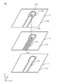
- FIG. 3 is an exploded perspective view of the first conductor layer, the circuit layer, and the second conductor layer.
- FIG. 4 is a diagram showing the first half of the manufacturing process of the high frequency circuit according to the embodiment.
- FIG. 5 is a diagram showing the latter half of the manufacturing process of the high frequency circuit according to the embodiment.
- FIG. 6 is a plan view showing a modified example of the high frequency circuit.
- FIG. 7 is a plan view of the high frequency circuit according to the comparative example.
- the shield via is formed by forming a large number of circular through holes in a plan view penetrating in the thickness direction of the dielectric substrate on the dielectric substrate and providing a conductor such as copper in the through holes.
- the shield via is used as an electromagnetic wave shield for preventing leakage of electromagnetic waves in a dielectric substrate.
- FIG. 7 shows an example of a structure in which a large number of shield vias 102 are formed so as to surround the signal transmission path 101 in the high frequency circuit 100 having the signal transmission path 101. Unnecessary electromagnetic waves are radiated from the high-frequency signal transmission line 101. Electromagnetic waves become noise for peripheral circuits and deteriorate the characteristics of peripheral circuits.
- the large number of shield vias 102 function as electromagnetic wave shields.
- the electromagnetic wave shield can shield the electromagnetic wave leaking from the signal transmission line 101.
- the high-frequency circuit has a first dielectric layer, a transmission path for high-frequency signals provided on the first dielectric layer, and a ground pattern arranged around the transmission path.
- the first dielectric layer is located between the second dielectric layer provided so that the circuit layer is located between the circuit layer provided and the first dielectric layer, and the circuit layer.
- a second conductor layer provided so that the second dielectric layer is located between the first conductor layer provided in the circuit layer and the circuit layer, and an electromagnetic wave shield provided around the transmission path. And. Since the circuit layer is sandwiched between the first conductor layer and the second conductor layer, leakage of electromagnetic waves from the transmission path in the thickness direction of the high frequency circuit is prevented.
- the electromagnetic wave shield has a ground conductor on the inner surface of the first dielectric layer, the ground pattern, the second dielectric layer, the first conductor layer, and a plurality of holes penetrating the second conductor layer. It is configured with.
- the plurality of holes are a plurality of elongated holes provided at intervals along the direction surrounding the transmission line, and each of the plurality of elongated holes has a width in a longitudinal dimension along the direction surrounding the transmission path. Larger than the dimensions. Since the holes through which the electromagnetic wave shield is formed are long along the direction surrounding the transmission path, electromagnetic wave leakage is efficient even if the number of holes is reduced compared to the case where a circular shield via is provided. Can be prevented.
- the longitudinal dimension is preferably larger than 5 times the width dimension.
- the longitudinal dimension is preferably larger than the interval.
- the longitudinal dimension is preferably larger than 5 times the interval.
- Each of the plurality of holes continuously penetrates the first dielectric layer, the ground pattern, the second dielectric layer, the first conductor layer, and the second conductor layer. Is preferable.
- the holes that penetrate continuously can prevent the leakage of electromagnetic waves more reliably.
- the electromagnetic wave shield includes at least a first shield provided around the transmission path and a second shield provided on the outer peripheral side of the first shield, and the first shield is the first shield.
- the ground conductor is provided on the inner surface of one dielectric layer, the ground pattern, the second dielectric layer, the first conductor layer, and a plurality of first holes penetrating the second conductor layer.
- the plurality of first holes are a plurality of first elongated holes provided at intervals along a direction surrounding the transmission path, and each of the plurality of first elongated holes is the transmission path.
- the longitudinal dimension along the direction surrounding the is larger than the width dimension, and the second shield has the first dielectric layer, the ground pattern, and the second dielectric layer on the outer peripheral side of the plurality of first holes.
- the ground conductor is provided on the inner surface of the first conductor layer and the plurality of second holes penetrating the second conductor layer, and the plurality of second holes have the transmission path.
- a plurality of second elongated holes provided at intervals along the surrounding direction, and each of the plurality of second elongated holes has a longitudinal dimension along the direction surrounding the transmission path larger than the width dimension.
- the second shield is preferably arranged so as to shield the leaked electromagnetic waves from between the plurality of first elongated holes. In this case, leakage of electromagnetic waves can be prevented more efficiently.
- the high frequency circuit further includes a cover film attached to at least one surface of the first conductor layer and the second conductor layer.
- the strength of the high frequency circuit in which the elongated holes are formed can be ensured by the cover film.
- the high frequency circuit 10 is configured as a flexible printed circuit (FPC) used for high frequency signal transmission.
- the FPC has a structure in which a conductor such as a copper foil is attached to a thin and soft insulator base film.
- the high frequency circuit 10 is not limited to the FPC, and may be a circuit formed on a rigid substrate.
- the high-frequency circuit 10 includes a first dielectric layer 11, a circuit layer 21, a second dielectric layer 12, a first conductor layer 31, a second conductor layer 32, and an electromagnetic wave shield. It is equipped with 150.
- the high frequency circuit 10 according to the embodiment has a multilayer structure having three conductor layers. The number of conductor layers is not particularly limited, and may be two layers, four layers, five layers, or more.
- the conductor layer arranged in the middle of the three conductor layers is a circuit layer 21 having a high-frequency transmission path 21A.
- a first conductor layer 31, which is one of the three conductor layers, is arranged on the lower side of FIG. 2, which is one side of the circuit layer 21 in the thickness direction.
- a second conductor layer 32, which is the remaining one of the three conductor layers, is arranged on the upper side of FIG. 2, which is the other side in the thickness direction of the circuit layer 21.
- the circuit layer 21 has a transmission line 21A and a ground pattern 21B located around the transmission line 21A.
- the space between the transmission line 21A and the ground pattern 21B is removed by etching, and the transmission line 21A and the ground pattern 21B are insulated from each other.
- the transmission line 21A is formed in a straight line in FIG. 3, it may be bent.
- a hole 21C that is a part of the hole 151 for the electromagnetic wave shield 150 described later is formed.
- a first dielectric layer 11 is provided between the circuit layer 21 and the first conductor layer 31. That is, the circuit layer 21 is provided on the first dielectric layer 11. In other words, the circuit layer 21 is provided above the first conductor layer 31 via the first dielectric layer 11. The circuit layer 21 and the first dielectric layer 11 are adhered to each other via an adhesive 60. As shown in FIG. 3, the first conductor layer 31 is substantially entirely formed of the ground pattern 31B except for the hole 31C which is a part of the hole 151 for the electromagnetic wave shield 150 described later. That is, the first conductor layer 31 is a ground layer.
- the adhesive 60 is preferably excellent in flexibility and heat resistance.
- the adhesive 60 is an adhesive of various resins such as a modified polyphenylene ether-based adhesive, a styrene resin-based adhesive, an epoxy resin-based adhesive, a butyral resin-based adhesive, and an acrylic resin-based adhesive.
- the main component of the adhesive 60 is preferably a thermosetting resin.
- the lower limit of the curing temperature of the thermosetting resin, which is the main component of the adhesive 60 is preferably 120 ° C, more preferably 150 ° C.
- the upper limit of the curing temperature of the thermosetting resin, which is the main component of the adhesive 60 is preferably 250 ° C, more preferably 230 ° C, and even more preferably 200 ° C.
- the curing temperature of the thermosetting resin, which is the main component of the adhesive 60 is higher than the above lower limit, the adhesive 60 can be easily handled.
- thermosetting resin which is the main component of the adhesive 60
- the curing temperature of the thermosetting resin which is the main component of the adhesive 60
- the lower limit of the relative permittivity of the adhesive 60 is preferably smaller, but in reality, 1.5 is considered to be the limit in order to satisfy other conditions such as insulation and mechanical strength.
- the upper limit of the relative permittivity of the adhesive 60 is, for example, 3, preferably 2.8, and more preferably 2.6. Further, when the relative permittivity of the adhesive 60 is smaller than the above upper limit, the dielectric loss can be suppressed when the high frequency signal is transmitted by the high frequency circuit 10.
- a second dielectric layer 12 is provided between the circuit layer 21 and the second conductor layer 32. That is, the second dielectric layer 12 is provided so that the circuit layer 21 is located between the second dielectric layer 12 and the first dielectric layer 11.
- the second conductor layer 32 is composed of the ground pattern 32B on almost the entire surface except for the transmission path 32A for the high frequency signal and the hole 32C which is a part of the hole 151 for the electromagnetic wave shield 150. Has been done. That is, the second conductor layer 32 is a ground layer.
- the first conductor layer 31 and the second conductor layer 32 that function as ground layers are provided on both the upper and lower sides of the circuit layer 21, that is, on both sides in the Z direction of FIG. Therefore, among the electromagnetic waves radiated from the transmission path 21A, the electromagnetic waves radiated on both sides in the thickness direction of the high frequency circuit 10, that is, on both sides in the Z direction in FIG. 2, are generated by the first conductor layer 31 and the second conductor layer 32. Be shielded.
- the high frequency circuit 10 of the embodiment includes an electromagnetic wave shield 150 for shielding electromagnetic waves radiated in a direction parallel to the XY plane.
- the XY plane is a plane perpendicular to the thickness direction of the high frequency circuit 10.
- the Z direction is the thickness direction of the high frequency circuit 10, and corresponds to the stacking direction in the above-mentioned multilayer structure of the conductor layer.
- the electromagnetic wave radiated in the Z direction is shielded by the first conductor layer 31 and the second conductor layer 32. Electromagnetic waves radiated in a direction parallel to the XY plane are shielded by the electromagnetic wave shield 150. Therefore, it is possible to effectively prevent the electromagnetic wave radiated from the transmission line 21A from leaking to the outside of the high frequency circuit 10. As a result, it is possible to suppress the influence of the leaked electromagnetic wave on other circuits in the vicinity.
- the electromagnetic wave shield 150 is configured to function as a shield wall that shields electromagnetic waves passing through the first dielectric layer 11 and the second dielectric layer 12 around the transmission line 21A. As shown in FIG. 1, the electromagnetic wave shield 150 is formed so as to surround the transmission line 21A in a plan view. In the embodiment, a plurality of electromagnetic wave shields 150 are provided at intervals D along the direction surrounding the transmission line 21A.
- the electromagnetic wave shield 150 penetrates the first dielectric layer 11, the ground pattern 21B of the circuit layer 21, the second dielectric layer 12, the first conductor layer 31, and the second conductor layer 32.
- a ground conductor 152 is provided on the inner surface of the hole 151.
- the ground conductor 152 is provided on the inner surface of the holes 151 formed in the ground patterns 31B and 32B. Since the ground conductor 152 exists so as to surround the transmission path 21A, it can shield electromagnetic waves passing through the first dielectric layer 11 and the second dielectric layer 12. On the lower side of FIG. 1, the transmission line 21A is not surrounded by the electromagnetic wave shield 150.
- the electromagnetic wave shield 150 can also surround the lower side of the transmission line 21A.
- the electromagnetic wave shield 150 has an elongated shape along the direction surrounding the transmission line 21A. That is, in each electromagnetic wave shield 150, the longitudinal dimension L along the direction surrounding the transmission path 21A is larger than the width dimension W. Therefore, the leaked electromagnetic wave can be effectively shielded by a smaller number of electromagnetic wave shields 150 as compared with the circular shield via 102.
- a fluororesin substrate with double-sided copper is prepared as an example of the substrate.
- the fluororesin substrate with double-sided copper includes a fluororesin substrate constituting the second dielectric layer 12, copper constituting the circuit layer 21, and copper constituting the second conductor layer 32.
- the material of the substrate is not limited to the fluororesin.
- step S12 through holes 41 penetrating the circuit layer 21, the second dielectric layer 12, and the second conductor layer 32 are formed at the positions of the transmission line 21A and the transmission line 32A.
- step S13 the inside of the through hole 41 is filled with a conductor by plating.
- a via 40 that electrically connects the transmission line 21A and the transmission line 32A is formed.
- the transmission line 32A functions as, for example, an external connection terminal for the transmission line 21A.
- the internal surface of the through hole 41 may be covered by plating, and the remaining space may be filled with synthetic resin.
- step S14 the circuit layer 21 and the second conductor layer 32 of the fluororesin substrate with double-sided copper are etched, and the transmission line 21A of the circuit layer 21 and the transmission line 32A of the second conductor layer 32 are subjected to etching processing. And are formed.
- a single-sided fluororesin substrate is bonded to the circuit layer 21 side.
- the single-sided fluororesin substrate includes a fluororesin substrate constituting the first dielectric layer 11 and copper constituting the first conductor layer 31.
- the first dielectric layer 11 and the circuit layer 21 are bonded to each other by the adhesive 60 so as to face each other.
- the adhesive 60 is, for example, a bonding sheet.
- the bonding sheet is used for bonding between layers of the substrate.
- the bonding sheet has insulating properties and adhesiveness.
- a plurality of holes 151 that continuously penetrate from the first conductor layer 31 to the second conductor layer 32 are formed by press punching.
- the method for forming the holes 151 is not limited to the press punching process, but it is advantageous to use the press punching process because a plurality of holes 151 can be formed at the same time.
- the hole 151 may be formed by laser processing.
- the plurality of holes 151 are provided at intervals D along the direction surrounding the transmission line 21A.
- Each of the plurality of holes 151 has a longitudinal dimension L along a direction surrounding the transmission line 21A and a width dimension W orthogonal to the direction of the longitudinal dimension L.
- Each of the plurality of holes 151 is an elongated hole. That is, each of the plurality of holes 151 has a longitudinal dimension L larger than a width dimension W.
- the longitudinal dimension L is preferably larger than 5 times the width dimension W, more preferably larger than 10 times the width dimension W, further preferably larger than 15 times the width dimension W, and the width dimension W. It is more preferably larger than 20 times.
- the longitudinal dimension L is larger than the interval D.
- the longitudinal dimension L is preferably larger than 5 times the interval D, preferably larger than 10 times the interval D, preferably larger than 15 times the interval D, and larger than 20 times the interval D. Is more preferable.
- the interval D is preferably smaller than 1/4 of the wavelength ⁇ of the high frequency transmitted by the transmission path 21A, and more preferably smaller than 1/8 of the wavelength ⁇ in order to suppress leakage of electromagnetic waves in the interval D. , It is more preferably smaller than 1/16 of the wavelength ⁇ . The smaller the interval D, the more the leakage of electromagnetic waves can be suppressed. By making the interval D smaller than 1/16 of the wavelength ⁇ , leakage of electromagnetic waves can be sufficiently reduced.
- the electromagnetic wave shield 150 becomes thicker, so that the allowable interval D becomes larger. That is, if the width dimension W is increased, the leakage of electromagnetic waves can be reduced even if the gap D between the plurality of holes 151 is the same.
- step S32 the conductor 152 is formed on the inner surface of the hole 151 by the plating process.
- FIG. 2 shows a case where the conductor 152 is provided in contact with the entire inner surface of the hole 151, and the conductor 152 is formed in a cylindrical shape having an outer peripheral shape corresponding to the inner peripheral shape of the hole 151.
- the conductor 152 may be formed only on the inner surface of the hole 151, or may be formed so as to completely fill the inside of the hole 151.
- the inside of the conductor 152 may be filled with a dielectric such as a synthetic resin, or may be filled with a conductor such as a conductive paste.
- the conductor 152 electrically connects the ground pattern 21B, the ground pattern 31B, and the ground pattern 32B. Therefore, the conductor 152 is a ground conductor 152.
- the ground conductor 152 is provided inside each of the plurality of holes 151 that surround the transmission path 21A. Therefore, the plurality of ground conductors 152 formed in the plurality of holes 151 function as the electromagnetic wave shield 150 surrounding the periphery of the transmission path 21A.
- the ground conductor 152 can shield electromagnetic waves radiated through the first dielectric layer 11 and the second dielectric layer 12.
- the conductor 152 electrically connects the ground pattern 21B of the circuit layer 21 and the ground pattern 31B of the first conductor layer 31. Therefore, since the conductor 152 has the same potential as the ground patterns 21B and 31B, it becomes the ground conductor 152. Since the ground conductor 152 is provided in the hole 151 surrounding the transmission line 21A, it functions as an electromagnetic wave shield 150 surrounding the transmission line 21A. The ground conductor 152 located in the first dielectric layer 11 can shield the electromagnetic waves radiated through the first dielectric layer 11.
- the conductor 152 electrically connects the ground pattern 21B of the circuit layer 21 and the ground pattern 32B of the second conductor layer 32. Therefore, since the conductor 152 has the same potential as the ground patterns 21B and 32B, it becomes the ground conductor 152. Since the ground conductor 152 is provided in the hole 151 surrounding the transmission line 21A, it functions as an electromagnetic wave shield 150 surrounding the transmission line 21A. The ground conductor 152 located in the second dielectric layer 12 can shield the electromagnetic waves radiated through the second dielectric layer 12.
- step S33 the cover films 71 and 72 are attached to the surfaces of the first conductor layer 31 and the second conductor layer 32, respectively, via the adhesives 81 and 82.
- the cover films 71 and 72 are made of polyimide, for example, and protect the first conductor layer 31 and the second conductor layer 32. By attaching the cover films 71 and 72, the strength of the high frequency circuit 10 in which the holes 151 are formed can be ensured.
- the plurality of electromagnetic wave shields 150 and holes 151 shown in FIG. 1 are formed so as to be surrounded by a single row around the transmission line 21A, but as shown in FIG. 6, even if they are formed so as to be surrounded by a plurality of rows. good.
- FIG. 6 shows a case where a plurality of electromagnetic wave shields 150 and holes 151 are arranged in two rows inside and outside.
- the electromagnetic wave shield 150 shown in FIG. 6 includes a first shield 150A provided around the transmission line 21A and a second shield 150B provided on the outer peripheral side of the first shield 150A. Another shield may be provided on the outer peripheral side of the second shield 150B.
- the first shield 150A is configured to include a ground conductor 152 on the inner surface of a plurality of first holes 151A that continuously penetrate from the first conductor layer 31 to the second conductor layer 32.
- Each of the plurality of first holes 151A is a long hole like the hole 151, and may be referred to as a first long hole here.
- the row consisting of the plurality of first holes 151A constitutes the first row provided at intervals along the direction surrounding the periphery of the transmission line 21A.
- each of the plurality of first elongated holes 151A has a longitudinal dimension L along the direction surrounding the transmission line 21A larger than the width dimension W.
- the second shield 150B is configured to include a ground conductor 152 on the inner surface of a plurality of second holes 151B that continuously penetrate from the first conductor layer 31 to the second conductor layer 32.
- Each of the plurality of second holes 151B is a long hole like the hole 151, and may be referred to as a second long hole here.
- the row consisting of the plurality of second holes 151B constitutes a second row provided at intervals along the direction surrounding the periphery of the transmission line 21A on the outer peripheral side of the plurality of first elongated holes 151A. ..
- each of the plurality of second elongated holes 151B has a longitudinal dimension L along the direction surrounding the transmission line 21A larger than the width dimension W.
- the second elongated hole 151B is arranged so as to exist at a corresponding position between the first elongated holes 151A. That is, the second elongated hole 151B is arranged so as to close the space between the first elongated holes 151A from the outer peripheral side of the first elongated hole 151A. Therefore, the second shield 150B composed of the ground conductor 152 in the second elongated hole 151B can shield the leakage electromagnetic wave from between the first shield 150A. As described above, in FIG. 6, the row of the second shield 150B, which is the outer electromagnetic wave shield, is arranged so as to shield the leaked electromagnetic wave from the row of the first shield 150A, which is the inner electromagnetic wave shield.
- the leaked electromagnetic waves can be efficiently shielded. Further, since the first hole 151A and the second hole 151B are elongated holes, the leaked electromagnetic wave can be efficiently shielded even with a small number of rows.
Landscapes
- Engineering & Computer Science (AREA)
- Microelectronics & Electronic Packaging (AREA)
- Physics & Mathematics (AREA)
- Electromagnetism (AREA)
- Manufacturing & Machinery (AREA)
- Shielding Devices Or Components To Electric Or Magnetic Fields (AREA)
Priority Applications (3)
| Application Number | Priority Date | Filing Date | Title |
|---|---|---|---|
| US17/783,138 US12389532B2 (en) | 2020-05-13 | 2021-05-10 | High-frequency circuit |
| CN202180007106.2A CN114788420B (zh) | 2020-05-13 | 2021-05-10 | 高频电路 |
| JP2022521913A JP7597800B2 (ja) | 2020-05-13 | 2021-05-10 | 高周波回路 |
Applications Claiming Priority (2)
| Application Number | Priority Date | Filing Date | Title |
|---|---|---|---|
| JP2020084545 | 2020-05-13 | ||
| JP2020-084545 | 2020-05-13 |
Publications (1)
| Publication Number | Publication Date |
|---|---|
| WO2021230215A1 true WO2021230215A1 (ja) | 2021-11-18 |
Family
ID=78524434
Family Applications (1)
| Application Number | Title | Priority Date | Filing Date |
|---|---|---|---|
| PCT/JP2021/017769 Ceased WO2021230215A1 (ja) | 2020-05-13 | 2021-05-10 | 高周波回路 |
Country Status (4)
| Country | Link |
|---|---|
| US (1) | US12389532B2 (https=) |
| JP (1) | JP7597800B2 (https=) |
| CN (1) | CN114788420B (https=) |
| WO (1) | WO2021230215A1 (https=) |
Cited By (2)
| Publication number | Priority date | Publication date | Assignee | Title |
|---|---|---|---|---|
| WO2023095797A1 (ja) * | 2021-11-24 | 2023-06-01 | 住友電気工業株式会社 | プリント配線板 |
| WO2023095798A1 (ja) * | 2021-11-24 | 2023-06-01 | 住友電気工業株式会社 | プリント配線板 |
Families Citing this family (2)
| Publication number | Priority date | Publication date | Assignee | Title |
|---|---|---|---|---|
| KR102908325B1 (ko) * | 2020-12-10 | 2026-01-05 | 삼성전기주식회사 | 인쇄회로기판 |
| US11758644B2 (en) * | 2021-05-13 | 2023-09-12 | Dell Products L.P. | Slotted vias for circuit boards |
Citations (5)
| Publication number | Priority date | Publication date | Assignee | Title |
|---|---|---|---|---|
| JP2003152292A (ja) * | 2001-11-19 | 2003-05-23 | Kyocera Corp | 配線基板 |
| JP2010506380A (ja) * | 2006-10-13 | 2010-02-25 | 日本電気株式会社 | 多層基板 |
| JP2014011528A (ja) * | 2012-06-28 | 2014-01-20 | Murata Mfg Co Ltd | 伝送線路 |
| JP2018200982A (ja) * | 2017-05-29 | 2018-12-20 | 東洋インキScホールディングス株式会社 | フレキシブルプリント配線板、フレキシブルプリント配線板の製造方法及び電子機器 |
| US20190269007A1 (en) * | 2018-02-28 | 2019-08-29 | Raytheon Company | Snap-rf interconnections |
Family Cites Families (20)
| Publication number | Priority date | Publication date | Assignee | Title |
|---|---|---|---|---|
| JPH04267586A (ja) | 1991-02-22 | 1992-09-24 | Nec Corp | 同軸配線パターンおよびその形成方法 |
| JP2605654B2 (ja) | 1995-03-31 | 1997-04-30 | 日本電気株式会社 | 複合マイクロ波回路モジュール及びその製造方法 |
| JP4195731B2 (ja) | 1996-07-25 | 2008-12-10 | 富士通株式会社 | 多層プリント板及びこれを利用した高周波回路装置 |
| JP3687041B2 (ja) * | 1997-04-16 | 2005-08-24 | 大日本印刷株式会社 | 配線基板、配線基板の製造方法、および半導体パッケージ |
| FI106585B (fi) * | 1997-10-22 | 2001-02-28 | Nokia Mobile Phones Ltd | Koaksiaalijohto, menetelmä koaksiaalijohdon valmistamiseksi ja langaton viestin |
| US6738598B2 (en) * | 2001-08-17 | 2004-05-18 | The Boeing Company | Multilayer radio frequency interconnect system |
| US20030188889A1 (en) * | 2002-04-09 | 2003-10-09 | Ppc Electronic Ag | Printed circuit board and method for producing it |
| JP3937433B2 (ja) * | 2002-09-17 | 2007-06-27 | 日本電気株式会社 | 平面回路−導波管接続構造 |
| JP2006067403A (ja) * | 2004-08-30 | 2006-03-09 | Kyocera Corp | 積層型開口面アンテナ |
| TWI248330B (en) * | 2005-01-14 | 2006-01-21 | Ind Tech Res Inst | High frequency and wide band impedance matching via |
| WO2007069789A1 (ja) * | 2005-12-16 | 2007-06-21 | Ibiden Co., Ltd. | 多層プリント配線板およびその製造方法 |
| JP4199796B2 (ja) * | 2006-10-30 | 2008-12-17 | 京セラ株式会社 | 高周波線路−導波管変換器 |
| JP2008244289A (ja) * | 2007-03-28 | 2008-10-09 | Mitsubishi Electric Corp | 電磁シールド構造 |
| CN101971327B (zh) * | 2008-03-17 | 2012-07-18 | 三菱电机株式会社 | 多层介质基板及半导体封装 |
| JP6537172B2 (ja) | 2015-06-01 | 2019-07-03 | 住友電工プリントサーキット株式会社 | プリント配線板 |
| US9992859B2 (en) * | 2015-09-25 | 2018-06-05 | Intel Corporation | Low loss and low cross talk transmission lines using shaped vias |
| KR102455653B1 (ko) * | 2015-12-08 | 2022-10-18 | 주식회사 기가레인 | 고주파 전송선로 |
| US11101533B2 (en) * | 2016-10-13 | 2021-08-24 | Win Semiconductors Corp. | Radio frequency device |
| JP2019029609A (ja) * | 2017-08-03 | 2019-02-21 | 日立化成株式会社 | 配線基板及びその製造方法 |
| JP2019197785A (ja) | 2018-05-08 | 2019-11-14 | 三菱電機株式会社 | プリント配線板 |
-
2021
- 2021-05-10 JP JP2022521913A patent/JP7597800B2/ja active Active
- 2021-05-10 WO PCT/JP2021/017769 patent/WO2021230215A1/ja not_active Ceased
- 2021-05-10 CN CN202180007106.2A patent/CN114788420B/zh active Active
- 2021-05-10 US US17/783,138 patent/US12389532B2/en active Active
Patent Citations (5)
| Publication number | Priority date | Publication date | Assignee | Title |
|---|---|---|---|---|
| JP2003152292A (ja) * | 2001-11-19 | 2003-05-23 | Kyocera Corp | 配線基板 |
| JP2010506380A (ja) * | 2006-10-13 | 2010-02-25 | 日本電気株式会社 | 多層基板 |
| JP2014011528A (ja) * | 2012-06-28 | 2014-01-20 | Murata Mfg Co Ltd | 伝送線路 |
| JP2018200982A (ja) * | 2017-05-29 | 2018-12-20 | 東洋インキScホールディングス株式会社 | フレキシブルプリント配線板、フレキシブルプリント配線板の製造方法及び電子機器 |
| US20190269007A1 (en) * | 2018-02-28 | 2019-08-29 | Raytheon Company | Snap-rf interconnections |
Cited By (2)
| Publication number | Priority date | Publication date | Assignee | Title |
|---|---|---|---|---|
| WO2023095797A1 (ja) * | 2021-11-24 | 2023-06-01 | 住友電気工業株式会社 | プリント配線板 |
| WO2023095798A1 (ja) * | 2021-11-24 | 2023-06-01 | 住友電気工業株式会社 | プリント配線板 |
Also Published As
| Publication number | Publication date |
|---|---|
| CN114788420A (zh) | 2022-07-22 |
| US12389532B2 (en) | 2025-08-12 |
| US20230019563A1 (en) | 2023-01-19 |
| JP7597800B2 (ja) | 2024-12-10 |
| JPWO2021230215A1 (https=) | 2021-11-18 |
| CN114788420B (zh) | 2025-03-18 |
Similar Documents
| Publication | Publication Date | Title |
|---|---|---|
| JP7597800B2 (ja) | 高周波回路 | |
| TWI778189B (zh) | 高頻傳輸用印刷線路板 | |
| US9692100B2 (en) | Multi-layer resin substrate having grounding conductors configured to form triplate line sections and microstrip sections | |
| JP5811306B1 (ja) | 信号伝送部品および電子機器 | |
| WO2016047492A1 (ja) | プリント配線板 | |
| CN111937230B (zh) | 多层传输线路 | |
| US9666925B2 (en) | Transmission line, a transmission line apparatus, and an electronic device | |
| CN110556198B (zh) | 屏蔽扁平电缆 | |
| US10219367B2 (en) | Multilayer resin substrate, and method of manufacturing multilayer resin substrate | |
| JPWO2020130010A1 (ja) | 伝送線路部材 | |
| JP4414365B2 (ja) | 高速伝送用基板 | |
| CN114846909B (zh) | 高频电路 | |
| CN106973483A (zh) | 柔性电路板及其制作方法 | |
| US11140769B1 (en) | Flexible circuit board and method for manufacturing the same | |
| JP2010170933A (ja) | フレキシブルフラットケーブル | |
| WO2021210297A1 (ja) | 多層基板 | |
| CN113273028B (zh) | 传输线路构造体 | |
| US20220077556A1 (en) | Transmission line and electronic device | |
| CN113131165B (zh) | 电路结构 | |
| JP2010016076A (ja) | フレキシブルプリント基板及びこれを備えたリジッドフレキシブルプリント基板 | |
| JP7827160B2 (ja) | アンテナモジュール | |
| JP7768019B2 (ja) | シールドフラットケーブル | |
| JP2011192709A (ja) | 半導体装置 | |
| WO2026048713A1 (ja) | 伝送線路及び電子機器 | |
| CN120711602A (zh) | 折叠式电路板及其制造方法 |
Legal Events
| Date | Code | Title | Description |
|---|---|---|---|
| 121 | Ep: the epo has been informed by wipo that ep was designated in this application |
Ref document number: 21802945 Country of ref document: EP Kind code of ref document: A1 |
|
| ENP | Entry into the national phase |
Ref document number: 2022521913 Country of ref document: JP Kind code of ref document: A |
|
| NENP | Non-entry into the national phase |
Ref country code: DE |
|
| 122 | Ep: pct application non-entry in european phase |
Ref document number: 21802945 Country of ref document: EP Kind code of ref document: A1 |
|
| WWG | Wipo information: grant in national office |
Ref document number: 202180007106.2 Country of ref document: CN |
|
| WWG | Wipo information: grant in national office |
Ref document number: 17783138 Country of ref document: US |