WO2021230215A1 - High frequency circuit - Google Patents
High frequency circuit Download PDFInfo
- Publication number
- WO2021230215A1 WO2021230215A1 PCT/JP2021/017769 JP2021017769W WO2021230215A1 WO 2021230215 A1 WO2021230215 A1 WO 2021230215A1 JP 2021017769 W JP2021017769 W JP 2021017769W WO 2021230215 A1 WO2021230215 A1 WO 2021230215A1
- Authority
- WO
- WIPO (PCT)
- Prior art keywords
- layer
- dielectric layer
- holes
- shield
- conductor
- Prior art date
Links
Images


Classifications
-
- H—ELECTRICITY
- H01—ELECTRIC ELEMENTS
- H01P—WAVEGUIDES; RESONATORS, LINES, OR OTHER DEVICES OF THE WAVEGUIDE TYPE
- H01P5/00—Coupling devices of the waveguide type
- H01P5/02—Coupling devices of the waveguide type with invariable factor of coupling
- H01P5/022—Transitions between lines of the same kind and shape, but with different dimensions
- H01P5/028—Transitions between lines of the same kind and shape, but with different dimensions between strip lines
-
- H—ELECTRICITY
- H05—ELECTRIC TECHNIQUES NOT OTHERWISE PROVIDED FOR
- H05K—PRINTED CIRCUITS; CASINGS OR CONSTRUCTIONAL DETAILS OF ELECTRIC APPARATUS; MANUFACTURE OF ASSEMBLAGES OF ELECTRICAL COMPONENTS
- H05K1/00—Printed circuits
- H05K1/02—Details
- H05K1/0213—Electrical arrangements not otherwise provided for
- H05K1/0237—High frequency adaptations
-
- H—ELECTRICITY
- H01—ELECTRIC ELEMENTS
- H01P—WAVEGUIDES; RESONATORS, LINES, OR OTHER DEVICES OF THE WAVEGUIDE TYPE
- H01P3/00—Waveguides; Transmission lines of the waveguide type
- H01P3/02—Waveguides; Transmission lines of the waveguide type with two longitudinal conductors
- H01P3/08—Microstrips; Strip lines
- H01P3/088—Stacked transmission lines
-
- H—ELECTRICITY
- H05—ELECTRIC TECHNIQUES NOT OTHERWISE PROVIDED FOR
- H05K—PRINTED CIRCUITS; CASINGS OR CONSTRUCTIONAL DETAILS OF ELECTRIC APPARATUS; MANUFACTURE OF ASSEMBLAGES OF ELECTRICAL COMPONENTS
- H05K1/00—Printed circuits
- H05K1/02—Details
- H05K1/0213—Electrical arrangements not otherwise provided for
- H05K1/0215—Grounding of printed circuits by connection to external grounding means
-
- H—ELECTRICITY
- H05—ELECTRIC TECHNIQUES NOT OTHERWISE PROVIDED FOR
- H05K—PRINTED CIRCUITS; CASINGS OR CONSTRUCTIONAL DETAILS OF ELECTRIC APPARATUS; MANUFACTURE OF ASSEMBLAGES OF ELECTRICAL COMPONENTS
- H05K1/00—Printed circuits
- H05K1/02—Details
- H05K1/0213—Electrical arrangements not otherwise provided for
- H05K1/0216—Reduction of cross-talk, noise or electromagnetic interference
- H05K1/0218—Reduction of cross-talk, noise or electromagnetic interference by printed shielding conductors, ground planes or power plane
- H05K1/0219—Printed shielding conductors for shielding around or between signal conductors, e.g. coplanar or coaxial printed shielding conductors
-
- H—ELECTRICITY
- H05—ELECTRIC TECHNIQUES NOT OTHERWISE PROVIDED FOR
- H05K—PRINTED CIRCUITS; CASINGS OR CONSTRUCTIONAL DETAILS OF ELECTRIC APPARATUS; MANUFACTURE OF ASSEMBLAGES OF ELECTRICAL COMPONENTS
- H05K3/00—Apparatus or processes for manufacturing printed circuits
- H05K3/40—Forming printed elements for providing electric connections to or between printed circuits
- H05K3/42—Plated through-holes or plated via connections
- H05K3/429—Plated through-holes specially for multilayer circuits, e.g. having connections to inner circuit layers
-
- H—ELECTRICITY
- H05—ELECTRIC TECHNIQUES NOT OTHERWISE PROVIDED FOR
- H05K—PRINTED CIRCUITS; CASINGS OR CONSTRUCTIONAL DETAILS OF ELECTRIC APPARATUS; MANUFACTURE OF ASSEMBLAGES OF ELECTRICAL COMPONENTS
- H05K9/00—Screening of apparatus or components against electric or magnetic fields
-
- H—ELECTRICITY
- H05—ELECTRIC TECHNIQUES NOT OTHERWISE PROVIDED FOR
- H05K—PRINTED CIRCUITS; CASINGS OR CONSTRUCTIONAL DETAILS OF ELECTRIC APPARATUS; MANUFACTURE OF ASSEMBLAGES OF ELECTRICAL COMPONENTS
- H05K1/00—Printed circuits
- H05K1/02—Details
- H05K1/0213—Electrical arrangements not otherwise provided for
- H05K1/0216—Reduction of cross-talk, noise or electromagnetic interference
- H05K1/0218—Reduction of cross-talk, noise or electromagnetic interference by printed shielding conductors, ground planes or power plane
- H05K1/0224—Patterned shielding planes, ground planes or power planes
- H05K1/0225—Single or multiple openings in a shielding, ground or power plane
-
- H—ELECTRICITY
- H05—ELECTRIC TECHNIQUES NOT OTHERWISE PROVIDED FOR
- H05K—PRINTED CIRCUITS; CASINGS OR CONSTRUCTIONAL DETAILS OF ELECTRIC APPARATUS; MANUFACTURE OF ASSEMBLAGES OF ELECTRICAL COMPONENTS
- H05K1/00—Printed circuits
- H05K1/02—Details
- H05K1/0213—Electrical arrangements not otherwise provided for
- H05K1/0237—High frequency adaptations
- H05K1/025—Impedance arrangements, e.g. impedance matching, reduction of parasitic impedance
- H05K1/0251—Impedance arrangements, e.g. impedance matching, reduction of parasitic impedance related to vias or transitions between vias and transmission lines
-
- H—ELECTRICITY
- H05—ELECTRIC TECHNIQUES NOT OTHERWISE PROVIDED FOR
- H05K—PRINTED CIRCUITS; CASINGS OR CONSTRUCTIONAL DETAILS OF ELECTRIC APPARATUS; MANUFACTURE OF ASSEMBLAGES OF ELECTRICAL COMPONENTS
- H05K1/00—Printed circuits
- H05K1/02—Details
- H05K1/11—Printed elements for providing electric connections to or between printed circuits
-
- H—ELECTRICITY
- H05—ELECTRIC TECHNIQUES NOT OTHERWISE PROVIDED FOR
- H05K—PRINTED CIRCUITS; CASINGS OR CONSTRUCTIONAL DETAILS OF ELECTRIC APPARATUS; MANUFACTURE OF ASSEMBLAGES OF ELECTRICAL COMPONENTS
- H05K2201/00—Indexing scheme relating to printed circuits covered by H05K1/00
- H05K2201/09—Shape and layout
- H05K2201/09209—Shape and layout details of conductors
- H05K2201/095—Conductive through-holes or vias
- H05K2201/09609—Via grid, i.e. two-dimensional array of vias or holes in a single plane
-
- H—ELECTRICITY
- H05—ELECTRIC TECHNIQUES NOT OTHERWISE PROVIDED FOR
- H05K—PRINTED CIRCUITS; CASINGS OR CONSTRUCTIONAL DETAILS OF ELECTRIC APPARATUS; MANUFACTURE OF ASSEMBLAGES OF ELECTRICAL COMPONENTS
- H05K2201/00—Indexing scheme relating to printed circuits covered by H05K1/00
- H05K2201/09—Shape and layout
- H05K2201/09209—Shape and layout details of conductors
- H05K2201/095—Conductive through-holes or vias
- H05K2201/09618—Via fence, i.e. one-dimensional array of vias
-
- H—ELECTRICITY
- H05—ELECTRIC TECHNIQUES NOT OTHERWISE PROVIDED FOR
- H05K—PRINTED CIRCUITS; CASINGS OR CONSTRUCTIONAL DETAILS OF ELECTRIC APPARATUS; MANUFACTURE OF ASSEMBLAGES OF ELECTRICAL COMPONENTS
- H05K2201/00—Indexing scheme relating to printed circuits covered by H05K1/00
- H05K2201/09—Shape and layout
- H05K2201/09818—Shape or layout details not covered by a single group of H05K2201/09009 - H05K2201/09809
- H05K2201/09854—Hole or via having special cross-section, e.g. elliptical
Definitions
- the present disclosure relates to high frequency circuits.
- This application claims priority based on Japanese Patent Application No. 2020-084545 of the Japanese application dated May 13, 2020, and incorporates all the contents described in the Japanese application.
- Patent Document 1 discloses a structure including a large number of shield vias electrically connected to the front surface ground and the back surface ground of the dielectric substrate.
- the high-frequency circuit of the present disclosure includes a first dielectric layer and a circuit layer provided on the first dielectric layer and having a high-frequency signal transmission path and a ground pattern arranged around the transmission path.
- the first dielectric layer is provided between the second dielectric layer provided so that the circuit layer is located between the first dielectric layer and the circuit layer.
- a second conductor layer provided so that the second dielectric layer is located between the first conductor layer and the circuit layer, and an electromagnetic wave shield provided around the transmission path are provided.
- the electromagnetic wave shield is provided on the inner surface of the first dielectric layer, the ground pattern, the second dielectric layer, the first conductor layer, and a plurality of holes penetrating the second conductor layer.
- the plurality of holes are configured to include a body, and the plurality of holes are a plurality of elongated holes provided at intervals along a direction surrounding the transmission path, and each of the plurality of elongated holes has the transmission path.
- the longitudinal dimension along the enclosing direction is larger than the width dimension.
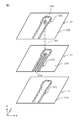
- FIG. 1 is a plan view of a high frequency circuit according to an embodiment.
- FIG. 2 is a cross-sectional view taken along the line BB of FIG.
- FIG. 3 is an exploded perspective view of the first conductor layer, the circuit layer, and the second conductor layer.
- FIG. 4 is a diagram showing the first half of the manufacturing process of the high frequency circuit according to the embodiment.
- FIG. 5 is a diagram showing the latter half of the manufacturing process of the high frequency circuit according to the embodiment.
- FIG. 6 is a plan view showing a modified example of the high frequency circuit.
- FIG. 7 is a plan view of the high frequency circuit according to the comparative example.
- the shield via is formed by forming a large number of circular through holes in a plan view penetrating in the thickness direction of the dielectric substrate on the dielectric substrate and providing a conductor such as copper in the through holes.
- the shield via is used as an electromagnetic wave shield for preventing leakage of electromagnetic waves in a dielectric substrate.
- FIG. 7 shows an example of a structure in which a large number of shield vias 102 are formed so as to surround the signal transmission path 101 in the high frequency circuit 100 having the signal transmission path 101. Unnecessary electromagnetic waves are radiated from the high-frequency signal transmission line 101. Electromagnetic waves become noise for peripheral circuits and deteriorate the characteristics of peripheral circuits.
- the large number of shield vias 102 function as electromagnetic wave shields.
- the electromagnetic wave shield can shield the electromagnetic wave leaking from the signal transmission line 101.
- the high-frequency circuit has a first dielectric layer, a transmission path for high-frequency signals provided on the first dielectric layer, and a ground pattern arranged around the transmission path.
- the first dielectric layer is located between the second dielectric layer provided so that the circuit layer is located between the circuit layer provided and the first dielectric layer, and the circuit layer.
- a second conductor layer provided so that the second dielectric layer is located between the first conductor layer provided in the circuit layer and the circuit layer, and an electromagnetic wave shield provided around the transmission path. And. Since the circuit layer is sandwiched between the first conductor layer and the second conductor layer, leakage of electromagnetic waves from the transmission path in the thickness direction of the high frequency circuit is prevented.
- the electromagnetic wave shield has a ground conductor on the inner surface of the first dielectric layer, the ground pattern, the second dielectric layer, the first conductor layer, and a plurality of holes penetrating the second conductor layer. It is configured with.
- the plurality of holes are a plurality of elongated holes provided at intervals along the direction surrounding the transmission line, and each of the plurality of elongated holes has a width in a longitudinal dimension along the direction surrounding the transmission path. Larger than the dimensions. Since the holes through which the electromagnetic wave shield is formed are long along the direction surrounding the transmission path, electromagnetic wave leakage is efficient even if the number of holes is reduced compared to the case where a circular shield via is provided. Can be prevented.
- the longitudinal dimension is preferably larger than 5 times the width dimension.
- the longitudinal dimension is preferably larger than the interval.
- the longitudinal dimension is preferably larger than 5 times the interval.
- Each of the plurality of holes continuously penetrates the first dielectric layer, the ground pattern, the second dielectric layer, the first conductor layer, and the second conductor layer. Is preferable.
- the holes that penetrate continuously can prevent the leakage of electromagnetic waves more reliably.
- the electromagnetic wave shield includes at least a first shield provided around the transmission path and a second shield provided on the outer peripheral side of the first shield, and the first shield is the first shield.
- the ground conductor is provided on the inner surface of one dielectric layer, the ground pattern, the second dielectric layer, the first conductor layer, and a plurality of first holes penetrating the second conductor layer.
- the plurality of first holes are a plurality of first elongated holes provided at intervals along a direction surrounding the transmission path, and each of the plurality of first elongated holes is the transmission path.
- the longitudinal dimension along the direction surrounding the is larger than the width dimension, and the second shield has the first dielectric layer, the ground pattern, and the second dielectric layer on the outer peripheral side of the plurality of first holes.
- the ground conductor is provided on the inner surface of the first conductor layer and the plurality of second holes penetrating the second conductor layer, and the plurality of second holes have the transmission path.
- a plurality of second elongated holes provided at intervals along the surrounding direction, and each of the plurality of second elongated holes has a longitudinal dimension along the direction surrounding the transmission path larger than the width dimension.
- the second shield is preferably arranged so as to shield the leaked electromagnetic waves from between the plurality of first elongated holes. In this case, leakage of electromagnetic waves can be prevented more efficiently.
- the high frequency circuit further includes a cover film attached to at least one surface of the first conductor layer and the second conductor layer.
- the strength of the high frequency circuit in which the elongated holes are formed can be ensured by the cover film.
- the high frequency circuit 10 is configured as a flexible printed circuit (FPC) used for high frequency signal transmission.
- the FPC has a structure in which a conductor such as a copper foil is attached to a thin and soft insulator base film.
- the high frequency circuit 10 is not limited to the FPC, and may be a circuit formed on a rigid substrate.
- the high-frequency circuit 10 includes a first dielectric layer 11, a circuit layer 21, a second dielectric layer 12, a first conductor layer 31, a second conductor layer 32, and an electromagnetic wave shield. It is equipped with 150.
- the high frequency circuit 10 according to the embodiment has a multilayer structure having three conductor layers. The number of conductor layers is not particularly limited, and may be two layers, four layers, five layers, or more.
- the conductor layer arranged in the middle of the three conductor layers is a circuit layer 21 having a high-frequency transmission path 21A.
- a first conductor layer 31, which is one of the three conductor layers, is arranged on the lower side of FIG. 2, which is one side of the circuit layer 21 in the thickness direction.
- a second conductor layer 32, which is the remaining one of the three conductor layers, is arranged on the upper side of FIG. 2, which is the other side in the thickness direction of the circuit layer 21.
- the circuit layer 21 has a transmission line 21A and a ground pattern 21B located around the transmission line 21A.
- the space between the transmission line 21A and the ground pattern 21B is removed by etching, and the transmission line 21A and the ground pattern 21B are insulated from each other.
- the transmission line 21A is formed in a straight line in FIG. 3, it may be bent.
- a hole 21C that is a part of the hole 151 for the electromagnetic wave shield 150 described later is formed.
- a first dielectric layer 11 is provided between the circuit layer 21 and the first conductor layer 31. That is, the circuit layer 21 is provided on the first dielectric layer 11. In other words, the circuit layer 21 is provided above the first conductor layer 31 via the first dielectric layer 11. The circuit layer 21 and the first dielectric layer 11 are adhered to each other via an adhesive 60. As shown in FIG. 3, the first conductor layer 31 is substantially entirely formed of the ground pattern 31B except for the hole 31C which is a part of the hole 151 for the electromagnetic wave shield 150 described later. That is, the first conductor layer 31 is a ground layer.
- the adhesive 60 is preferably excellent in flexibility and heat resistance.
- the adhesive 60 is an adhesive of various resins such as a modified polyphenylene ether-based adhesive, a styrene resin-based adhesive, an epoxy resin-based adhesive, a butyral resin-based adhesive, and an acrylic resin-based adhesive.
- the main component of the adhesive 60 is preferably a thermosetting resin.
- the lower limit of the curing temperature of the thermosetting resin, which is the main component of the adhesive 60 is preferably 120 ° C, more preferably 150 ° C.
- the upper limit of the curing temperature of the thermosetting resin, which is the main component of the adhesive 60 is preferably 250 ° C, more preferably 230 ° C, and even more preferably 200 ° C.
- the curing temperature of the thermosetting resin, which is the main component of the adhesive 60 is higher than the above lower limit, the adhesive 60 can be easily handled.
- thermosetting resin which is the main component of the adhesive 60
- the curing temperature of the thermosetting resin which is the main component of the adhesive 60
- the lower limit of the relative permittivity of the adhesive 60 is preferably smaller, but in reality, 1.5 is considered to be the limit in order to satisfy other conditions such as insulation and mechanical strength.
- the upper limit of the relative permittivity of the adhesive 60 is, for example, 3, preferably 2.8, and more preferably 2.6. Further, when the relative permittivity of the adhesive 60 is smaller than the above upper limit, the dielectric loss can be suppressed when the high frequency signal is transmitted by the high frequency circuit 10.
- a second dielectric layer 12 is provided between the circuit layer 21 and the second conductor layer 32. That is, the second dielectric layer 12 is provided so that the circuit layer 21 is located between the second dielectric layer 12 and the first dielectric layer 11.
- the second conductor layer 32 is composed of the ground pattern 32B on almost the entire surface except for the transmission path 32A for the high frequency signal and the hole 32C which is a part of the hole 151 for the electromagnetic wave shield 150. Has been done. That is, the second conductor layer 32 is a ground layer.
- the first conductor layer 31 and the second conductor layer 32 that function as ground layers are provided on both the upper and lower sides of the circuit layer 21, that is, on both sides in the Z direction of FIG. Therefore, among the electromagnetic waves radiated from the transmission path 21A, the electromagnetic waves radiated on both sides in the thickness direction of the high frequency circuit 10, that is, on both sides in the Z direction in FIG. 2, are generated by the first conductor layer 31 and the second conductor layer 32. Be shielded.
- the high frequency circuit 10 of the embodiment includes an electromagnetic wave shield 150 for shielding electromagnetic waves radiated in a direction parallel to the XY plane.
- the XY plane is a plane perpendicular to the thickness direction of the high frequency circuit 10.
- the Z direction is the thickness direction of the high frequency circuit 10, and corresponds to the stacking direction in the above-mentioned multilayer structure of the conductor layer.
- the electromagnetic wave radiated in the Z direction is shielded by the first conductor layer 31 and the second conductor layer 32. Electromagnetic waves radiated in a direction parallel to the XY plane are shielded by the electromagnetic wave shield 150. Therefore, it is possible to effectively prevent the electromagnetic wave radiated from the transmission line 21A from leaking to the outside of the high frequency circuit 10. As a result, it is possible to suppress the influence of the leaked electromagnetic wave on other circuits in the vicinity.
- the electromagnetic wave shield 150 is configured to function as a shield wall that shields electromagnetic waves passing through the first dielectric layer 11 and the second dielectric layer 12 around the transmission line 21A. As shown in FIG. 1, the electromagnetic wave shield 150 is formed so as to surround the transmission line 21A in a plan view. In the embodiment, a plurality of electromagnetic wave shields 150 are provided at intervals D along the direction surrounding the transmission line 21A.
- the electromagnetic wave shield 150 penetrates the first dielectric layer 11, the ground pattern 21B of the circuit layer 21, the second dielectric layer 12, the first conductor layer 31, and the second conductor layer 32.
- a ground conductor 152 is provided on the inner surface of the hole 151.
- the ground conductor 152 is provided on the inner surface of the holes 151 formed in the ground patterns 31B and 32B. Since the ground conductor 152 exists so as to surround the transmission path 21A, it can shield electromagnetic waves passing through the first dielectric layer 11 and the second dielectric layer 12. On the lower side of FIG. 1, the transmission line 21A is not surrounded by the electromagnetic wave shield 150.
- the electromagnetic wave shield 150 can also surround the lower side of the transmission line 21A.
- the electromagnetic wave shield 150 has an elongated shape along the direction surrounding the transmission line 21A. That is, in each electromagnetic wave shield 150, the longitudinal dimension L along the direction surrounding the transmission path 21A is larger than the width dimension W. Therefore, the leaked electromagnetic wave can be effectively shielded by a smaller number of electromagnetic wave shields 150 as compared with the circular shield via 102.
- a fluororesin substrate with double-sided copper is prepared as an example of the substrate.
- the fluororesin substrate with double-sided copper includes a fluororesin substrate constituting the second dielectric layer 12, copper constituting the circuit layer 21, and copper constituting the second conductor layer 32.
- the material of the substrate is not limited to the fluororesin.
- step S12 through holes 41 penetrating the circuit layer 21, the second dielectric layer 12, and the second conductor layer 32 are formed at the positions of the transmission line 21A and the transmission line 32A.
- step S13 the inside of the through hole 41 is filled with a conductor by plating.
- a via 40 that electrically connects the transmission line 21A and the transmission line 32A is formed.
- the transmission line 32A functions as, for example, an external connection terminal for the transmission line 21A.
- the internal surface of the through hole 41 may be covered by plating, and the remaining space may be filled with synthetic resin.
- step S14 the circuit layer 21 and the second conductor layer 32 of the fluororesin substrate with double-sided copper are etched, and the transmission line 21A of the circuit layer 21 and the transmission line 32A of the second conductor layer 32 are subjected to etching processing. And are formed.
- a single-sided fluororesin substrate is bonded to the circuit layer 21 side.
- the single-sided fluororesin substrate includes a fluororesin substrate constituting the first dielectric layer 11 and copper constituting the first conductor layer 31.
- the first dielectric layer 11 and the circuit layer 21 are bonded to each other by the adhesive 60 so as to face each other.
- the adhesive 60 is, for example, a bonding sheet.
- the bonding sheet is used for bonding between layers of the substrate.
- the bonding sheet has insulating properties and adhesiveness.
- a plurality of holes 151 that continuously penetrate from the first conductor layer 31 to the second conductor layer 32 are formed by press punching.
- the method for forming the holes 151 is not limited to the press punching process, but it is advantageous to use the press punching process because a plurality of holes 151 can be formed at the same time.
- the hole 151 may be formed by laser processing.
- the plurality of holes 151 are provided at intervals D along the direction surrounding the transmission line 21A.
- Each of the plurality of holes 151 has a longitudinal dimension L along a direction surrounding the transmission line 21A and a width dimension W orthogonal to the direction of the longitudinal dimension L.
- Each of the plurality of holes 151 is an elongated hole. That is, each of the plurality of holes 151 has a longitudinal dimension L larger than a width dimension W.
- the longitudinal dimension L is preferably larger than 5 times the width dimension W, more preferably larger than 10 times the width dimension W, further preferably larger than 15 times the width dimension W, and the width dimension W. It is more preferably larger than 20 times.
- the longitudinal dimension L is larger than the interval D.
- the longitudinal dimension L is preferably larger than 5 times the interval D, preferably larger than 10 times the interval D, preferably larger than 15 times the interval D, and larger than 20 times the interval D. Is more preferable.
- the interval D is preferably smaller than 1/4 of the wavelength ⁇ of the high frequency transmitted by the transmission path 21A, and more preferably smaller than 1/8 of the wavelength ⁇ in order to suppress leakage of electromagnetic waves in the interval D. , It is more preferably smaller than 1/16 of the wavelength ⁇ . The smaller the interval D, the more the leakage of electromagnetic waves can be suppressed. By making the interval D smaller than 1/16 of the wavelength ⁇ , leakage of electromagnetic waves can be sufficiently reduced.
- the electromagnetic wave shield 150 becomes thicker, so that the allowable interval D becomes larger. That is, if the width dimension W is increased, the leakage of electromagnetic waves can be reduced even if the gap D between the plurality of holes 151 is the same.
- step S32 the conductor 152 is formed on the inner surface of the hole 151 by the plating process.
- FIG. 2 shows a case where the conductor 152 is provided in contact with the entire inner surface of the hole 151, and the conductor 152 is formed in a cylindrical shape having an outer peripheral shape corresponding to the inner peripheral shape of the hole 151.
- the conductor 152 may be formed only on the inner surface of the hole 151, or may be formed so as to completely fill the inside of the hole 151.
- the inside of the conductor 152 may be filled with a dielectric such as a synthetic resin, or may be filled with a conductor such as a conductive paste.
- the conductor 152 electrically connects the ground pattern 21B, the ground pattern 31B, and the ground pattern 32B. Therefore, the conductor 152 is a ground conductor 152.
- the ground conductor 152 is provided inside each of the plurality of holes 151 that surround the transmission path 21A. Therefore, the plurality of ground conductors 152 formed in the plurality of holes 151 function as the electromagnetic wave shield 150 surrounding the periphery of the transmission path 21A.
- the ground conductor 152 can shield electromagnetic waves radiated through the first dielectric layer 11 and the second dielectric layer 12.
- the conductor 152 electrically connects the ground pattern 21B of the circuit layer 21 and the ground pattern 31B of the first conductor layer 31. Therefore, since the conductor 152 has the same potential as the ground patterns 21B and 31B, it becomes the ground conductor 152. Since the ground conductor 152 is provided in the hole 151 surrounding the transmission line 21A, it functions as an electromagnetic wave shield 150 surrounding the transmission line 21A. The ground conductor 152 located in the first dielectric layer 11 can shield the electromagnetic waves radiated through the first dielectric layer 11.
- the conductor 152 electrically connects the ground pattern 21B of the circuit layer 21 and the ground pattern 32B of the second conductor layer 32. Therefore, since the conductor 152 has the same potential as the ground patterns 21B and 32B, it becomes the ground conductor 152. Since the ground conductor 152 is provided in the hole 151 surrounding the transmission line 21A, it functions as an electromagnetic wave shield 150 surrounding the transmission line 21A. The ground conductor 152 located in the second dielectric layer 12 can shield the electromagnetic waves radiated through the second dielectric layer 12.
- step S33 the cover films 71 and 72 are attached to the surfaces of the first conductor layer 31 and the second conductor layer 32, respectively, via the adhesives 81 and 82.
- the cover films 71 and 72 are made of polyimide, for example, and protect the first conductor layer 31 and the second conductor layer 32. By attaching the cover films 71 and 72, the strength of the high frequency circuit 10 in which the holes 151 are formed can be ensured.
- the plurality of electromagnetic wave shields 150 and holes 151 shown in FIG. 1 are formed so as to be surrounded by a single row around the transmission line 21A, but as shown in FIG. 6, even if they are formed so as to be surrounded by a plurality of rows. good.
- FIG. 6 shows a case where a plurality of electromagnetic wave shields 150 and holes 151 are arranged in two rows inside and outside.
- the electromagnetic wave shield 150 shown in FIG. 6 includes a first shield 150A provided around the transmission line 21A and a second shield 150B provided on the outer peripheral side of the first shield 150A. Another shield may be provided on the outer peripheral side of the second shield 150B.
- the first shield 150A is configured to include a ground conductor 152 on the inner surface of a plurality of first holes 151A that continuously penetrate from the first conductor layer 31 to the second conductor layer 32.
- Each of the plurality of first holes 151A is a long hole like the hole 151, and may be referred to as a first long hole here.
- the row consisting of the plurality of first holes 151A constitutes the first row provided at intervals along the direction surrounding the periphery of the transmission line 21A.
- each of the plurality of first elongated holes 151A has a longitudinal dimension L along the direction surrounding the transmission line 21A larger than the width dimension W.
- the second shield 150B is configured to include a ground conductor 152 on the inner surface of a plurality of second holes 151B that continuously penetrate from the first conductor layer 31 to the second conductor layer 32.
- Each of the plurality of second holes 151B is a long hole like the hole 151, and may be referred to as a second long hole here.
- the row consisting of the plurality of second holes 151B constitutes a second row provided at intervals along the direction surrounding the periphery of the transmission line 21A on the outer peripheral side of the plurality of first elongated holes 151A. ..
- each of the plurality of second elongated holes 151B has a longitudinal dimension L along the direction surrounding the transmission line 21A larger than the width dimension W.
- the second elongated hole 151B is arranged so as to exist at a corresponding position between the first elongated holes 151A. That is, the second elongated hole 151B is arranged so as to close the space between the first elongated holes 151A from the outer peripheral side of the first elongated hole 151A. Therefore, the second shield 150B composed of the ground conductor 152 in the second elongated hole 151B can shield the leakage electromagnetic wave from between the first shield 150A. As described above, in FIG. 6, the row of the second shield 150B, which is the outer electromagnetic wave shield, is arranged so as to shield the leaked electromagnetic wave from the row of the first shield 150A, which is the inner electromagnetic wave shield.
- the leaked electromagnetic waves can be efficiently shielded. Further, since the first hole 151A and the second hole 151B are elongated holes, the leaked electromagnetic wave can be efficiently shielded even with a small number of rows.
Landscapes
- Engineering & Computer Science (AREA)
- Microelectronics & Electronic Packaging (AREA)
- Physics & Mathematics (AREA)
- Electromagnetism (AREA)
- Manufacturing & Machinery (AREA)
- Shielding Devices Or Components To Electric Or Magnetic Fields (AREA)
Abstract
Description
本開示は、高周波回路に関する。
本出願は、2020年05月13日付の日本国出願の特願2020-084545に基づく優先権を主張し、前記日本国出願に記載された全ての記載内容を援用するものである。
The present disclosure relates to high frequency circuits.
This application claims priority based on Japanese Patent Application No. 2020-084545 of the Japanese application dated May 13, 2020, and incorporates all the contents described in the Japanese application.
特許文献1は、誘電体基板の表面グランド及び裏面グランドに電気的に接続された多数のシールドビアを備えた構造を開示している。 Patent Document 1 discloses a structure including a large number of shield vias electrically connected to the front surface ground and the back surface ground of the dielectric substrate.
本開示のある側面は、高周波回路である。本開示の高周波回路は、第1誘電体層と、前記第1誘電体層上に設けられており、高周波信号の伝送路と前記伝送路の周囲に配置されたグランドパターンとを備える回路層と、前記第1誘電体層との間に前記回路層が位置するように設けられた第2誘電体層と、前記回路層との間に前記第1誘電体層が位置するように設けられた第1導電体層と、前記回路層との間に前記第2誘電体層が位置するように設けられた第2導電体層と、前記伝送路の周囲に設けられた電磁波シールドと、を備え、前記電磁波シールドは、前記第1誘電体層、前記グランドパターン、前記第2誘電体層、前記第1導電体層、及び前記第2導電体層を貫通した複数の孔の内面に、グランド導電体を備えて構成されており、前記複数の孔は、前記伝送路を囲む向きに沿って間隔をおいて設けられた複数の長孔であり、前記複数の長孔それぞれは、前記伝送路を囲む向きに沿った長手寸法が幅寸法よりも大きい。 One aspect of this disclosure is the high frequency circuit. The high-frequency circuit of the present disclosure includes a first dielectric layer and a circuit layer provided on the first dielectric layer and having a high-frequency signal transmission path and a ground pattern arranged around the transmission path. , The first dielectric layer is provided between the second dielectric layer provided so that the circuit layer is located between the first dielectric layer and the circuit layer. A second conductor layer provided so that the second dielectric layer is located between the first conductor layer and the circuit layer, and an electromagnetic wave shield provided around the transmission path are provided. The electromagnetic wave shield is provided on the inner surface of the first dielectric layer, the ground pattern, the second dielectric layer, the first conductor layer, and a plurality of holes penetrating the second conductor layer. The plurality of holes are configured to include a body, and the plurality of holes are a plurality of elongated holes provided at intervals along a direction surrounding the transmission path, and each of the plurality of elongated holes has the transmission path. The longitudinal dimension along the enclosing direction is larger than the width dimension.
[本開示が解決しようとする課題]
シールドビアは、誘電体基板の厚さ方向に貫通する平面視円形のスルーホールを誘電体基板に多数形成し、スルーホール内に銅などの導電体を設けることによって形成される。シールドビアは、誘電体基板における電磁波の漏洩を防止する電磁波シールドとして用いられる。
[Problems to be solved by this disclosure]
The shield via is formed by forming a large number of circular through holes in a plan view penetrating in the thickness direction of the dielectric substrate on the dielectric substrate and providing a conductor such as copper in the through holes. The shield via is used as an electromagnetic wave shield for preventing leakage of electromagnetic waves in a dielectric substrate.
図7は、信号伝送路101を有する高周波回路100において、信号伝送路101を囲むように多数のシールドビア102が形成された構造の例を示している。高周波の信号伝送路101からは、不要な電磁波が放射される。電磁波は、周辺の回路にとってノイズとなり、周辺の回路の特性を劣化させる。
FIG. 7 shows an example of a structure in which a large number of
信号伝送路101の周辺に多数のシールドビア102が設けられていると、多数のシールドビア102が、電磁波シールドとして機能する。この電磁波シールドによって信号伝送路101から漏洩する電磁波を遮蔽することができる。
When a large number of
ただし、シールドビア102同士の間からは、電磁波の漏洩が生じるおそれがある。電磁波の漏洩をより確実に防止するため、図7に示すように、信号伝送路101の周囲において複数列のシールドビア102を並列に配置することが考えられる。この場合、シールドビア102の数が非常に多くなるという問題が生じる。シールドビア102の数が多くなると、シールドビア102のための孔を大量に形成する必要があり、回路の製造効率を低下させる。
However, there is a risk of electromagnetic waves leaking between the
一方、回路の製造効率の観点から、シールドビア102の数を少なくすると、シールドビア102同士の間から、電磁波が漏洩し易くなり、電磁波の遮蔽性が損なわれる。
On the other hand, if the number of
したがって、電磁波の漏洩を効率的に防止することが望まれる。 Therefore, it is desired to efficiently prevent the leakage of electromagnetic waves.
[本開示の効果]
本開示によれば、電磁波の漏洩を効率的に防止できる。
[Effect of this disclosure]
According to the present disclosure, leakage of electromagnetic waves can be efficiently prevented.
[1.本開示の実施形態の説明] [1. Description of the Embodiments of the present disclosure]
(1)実施形態に係る高周波回路は、第1誘電体層と、前記第1誘電体層上に設けられており、高周波信号の伝送路と前記伝送路の周囲に配置されたグランドパターンとを備える回路層と、前記第1誘電体層との間に前記回路層が位置するように設けられた第2誘電体層と、前記回路層との間に前記第1誘電体層が位置するように設けられた第1導電体層と、前記回路層との間に前記第2誘電体層が位置するように設けられた第2導電体層と、前記伝送路の周囲に設けられた電磁波シールドと、を備える。回路層は、第1導電体層及び第2導電体層によって挟まれているため、伝送路から高周波回路の厚さ方向への電磁波の漏洩が防止される。前記電磁波シールドは、前記第1誘電体層、前記グランドパターン、前記第2誘電体層、前記第1導電体層、及び前記第2導電体層を貫通した複数の孔の内面に、グランド導電体を備えて構成されている。前記複数の孔は、前記伝送路を囲む向きに沿って間隔をおいて設けられた複数の長孔であり、前記複数の長孔それぞれは、前記伝送路を囲む向きに沿った長手寸法が幅寸法よりも大きい。電磁波シールドが形成される孔が伝送路を囲む向きに沿って長く形成されていることで、円形のシールドビアを設ける場合に比べて、孔の数を少なくしても、電磁波の漏洩を効率的に防止できる。 (1) The high-frequency circuit according to the embodiment has a first dielectric layer, a transmission path for high-frequency signals provided on the first dielectric layer, and a ground pattern arranged around the transmission path. The first dielectric layer is located between the second dielectric layer provided so that the circuit layer is located between the circuit layer provided and the first dielectric layer, and the circuit layer. A second conductor layer provided so that the second dielectric layer is located between the first conductor layer provided in the circuit layer and the circuit layer, and an electromagnetic wave shield provided around the transmission path. And. Since the circuit layer is sandwiched between the first conductor layer and the second conductor layer, leakage of electromagnetic waves from the transmission path in the thickness direction of the high frequency circuit is prevented. The electromagnetic wave shield has a ground conductor on the inner surface of the first dielectric layer, the ground pattern, the second dielectric layer, the first conductor layer, and a plurality of holes penetrating the second conductor layer. It is configured with. The plurality of holes are a plurality of elongated holes provided at intervals along the direction surrounding the transmission line, and each of the plurality of elongated holes has a width in a longitudinal dimension along the direction surrounding the transmission path. Larger than the dimensions. Since the holes through which the electromagnetic wave shield is formed are long along the direction surrounding the transmission path, electromagnetic wave leakage is efficient even if the number of holes is reduced compared to the case where a circular shield via is provided. Can be prevented.
(2)前記長手寸法は、前記幅寸法の5倍よりも大きいのが好ましい。孔の長手寸法を孔の幅寸法の5倍よりも大きくすることで、孔が十分に長くなり、電磁波の漏洩を効率的に防止できる。 (2) The longitudinal dimension is preferably larger than 5 times the width dimension. By making the longitudinal dimension of the hole larger than 5 times the width dimension of the hole, the hole becomes sufficiently long and the leakage of electromagnetic waves can be efficiently prevented.
(3)前記長手寸法は、前記間隔よりも大きいのが好ましい。孔の長手寸法を孔の間隔よりも大きくすることで、電磁波の漏洩を効率的に防止できる。 (3) The longitudinal dimension is preferably larger than the interval. By making the longitudinal dimension of the holes larger than the distance between the holes, it is possible to efficiently prevent the leakage of electromagnetic waves.
(4)前記長手寸法は、前記間隔の5倍よりも大きいのが好ましい。孔の長手寸法を孔の間隔の5倍よりも大きくすることで、電磁波の漏洩を効率的に防止できる。 (4) The longitudinal dimension is preferably larger than 5 times the interval. By making the longitudinal dimension of the holes larger than 5 times the distance between the holes, it is possible to efficiently prevent the leakage of electromagnetic waves.
(5)前記複数の孔それぞれは、前記第1誘電体層、前記グランドパターン、前記第2誘電体層、前記第1導電体層、及び前記第2導電体層を連続的に貫通しているのが好ましい。連続的に貫通した孔によって、電磁波の漏洩をより確実に防止できる。 (5) Each of the plurality of holes continuously penetrates the first dielectric layer, the ground pattern, the second dielectric layer, the first conductor layer, and the second conductor layer. Is preferable. The holes that penetrate continuously can prevent the leakage of electromagnetic waves more reliably.
(6)前記電磁波シールドは、前記伝送路の周囲に設けられた第1シールドと、前記第1シールドの外周側に設けられた第2シールドと、を少なくとも備え、前記第1シールドは、前記第1誘電体層、前記グランドパターン、前記第2誘電体層、前記第1導電体層、及び前記第2導電体層を貫通した複数の第1孔の内面に、前記グランド導電体を備えて構成されており、前記複数の第1孔は、前記伝送路を囲む向きに沿って間隔をおいて設けられた複数の第1長孔であり、前記複数の第1長孔それぞれは、前記伝送路を囲む向きに沿った長手寸法が幅寸法よりも大きく、前記第2シールドは、前記複数の第1孔の外周側において、前記第1誘電体層、前記グランドパターン、前記第2誘電体層、前記第1導電体層、及び前記第2導電体層を貫通した複数の第2孔の内面に、前記グランド導電体を備えて構成されており、前記複数の第2孔は、前記伝送路を囲む向きに沿って間隔をおいて設けられた複数の第2長孔であり、前記複数の第2長孔それぞれは、前記伝送路を囲む向きに沿った長手寸法が幅寸法よりも大きく、前記第2シールドは、前記複数の第1長孔の間からの漏洩電磁波を遮蔽するよう配置されているのが好ましい。この場合、電磁波の漏洩をより効率的に防止できる。 (6) The electromagnetic wave shield includes at least a first shield provided around the transmission path and a second shield provided on the outer peripheral side of the first shield, and the first shield is the first shield. The ground conductor is provided on the inner surface of one dielectric layer, the ground pattern, the second dielectric layer, the first conductor layer, and a plurality of first holes penetrating the second conductor layer. The plurality of first holes are a plurality of first elongated holes provided at intervals along a direction surrounding the transmission path, and each of the plurality of first elongated holes is the transmission path. The longitudinal dimension along the direction surrounding the is larger than the width dimension, and the second shield has the first dielectric layer, the ground pattern, and the second dielectric layer on the outer peripheral side of the plurality of first holes. The ground conductor is provided on the inner surface of the first conductor layer and the plurality of second holes penetrating the second conductor layer, and the plurality of second holes have the transmission path. A plurality of second elongated holes provided at intervals along the surrounding direction, and each of the plurality of second elongated holes has a longitudinal dimension along the direction surrounding the transmission path larger than the width dimension. The second shield is preferably arranged so as to shield the leaked electromagnetic waves from between the plurality of first elongated holes. In this case, leakage of electromagnetic waves can be prevented more efficiently.
(7)高周波回路は、前記第1導電体層及び前記第2導電体層の少なくとも一方の表面に貼付されたカバーフィルムを更に備えるのが好ましい。この場合、長孔が形成された高周波回路の強度をカバーフィルムによって確保できる。 (7) It is preferable that the high frequency circuit further includes a cover film attached to at least one surface of the first conductor layer and the second conductor layer. In this case, the strength of the high frequency circuit in which the elongated holes are formed can be ensured by the cover film.
[2.本開示の実施形態の詳細] [2. Details of Embodiments of the present disclosure]
以下、図面において同一符号は同一名称物を意味する。
図1から図6は、実施形態に係る高周波回路10を示している。実施形態に係る高周波回路10は、高周波信号伝送に用いられるフレキシブルプリントサーキット(FPC)として構成されている。FPCは、薄く柔らかい絶縁体ベースフィルムに銅箔などの導体が貼り付けられた構造を持つ。なお、高周波回路10は、FPCに限られず、リジット基板に形成された回路であってもよい。
Hereinafter, in the drawings, the same reference numerals mean the same names.
1 to 6 show a
図2に示すように、実施形態に係る高周波回路10は、第1誘電体層11と回路層21と第2誘電体層12と第1導電体層31と第2導電体層32と電磁波シールド150とを備える。実施形態に係る高周波回路10は、3層の導電体層を有する多層構造を持つ。なお、導電体層の数は、特に限定されず、2層、4層、5層、又はそれ以上であってもよい。図2において、3層の導電体層のうち中間に配置されている導電体層は、高周波の伝送路21Aを有する回路層21である。回路層21の厚さ方向の一方側である図2の下側には3層の導電体層のうちの一つである第1導電体層31が配置されている。回路層21の厚さ方向の他方側である図2の上側には3層の導電体層のうちの残り一つである第2導電体層32が配置されている。
As shown in FIG. 2, the high-
図3に示すように、回路層21は、伝送路21Aと、伝送路21Aの周囲に位置するグランドパターン21Bと、を有する。伝送路21Aとグランドパターン21Bとの間は、エッチングにより除去されており、伝送路21Aとグランドパターン21Bとは絶縁されている。なお、図3において、伝送路21Aは、直線状に形成されているが、屈曲形成されていてもよい。伝送路21Aの周囲には、後述の電磁波シールド150のための孔151の一部となる孔21Cが形成されている。
As shown in FIG. 3, the
図2に示すように回路層21と第1導電体層31との間には第1誘電体層11が設けられている。すなわち、回路層21は、第1誘電体層11上に設けられている。換言すると、回路層21は、第1誘電体層11を介して、第1導電体層31よりも上に設けられている。なお、回路層21と第1誘電体層11とは接着剤60を介して接着されている。図3に示すように第1導電体層31は、後述の電磁波シールド150のための孔151の一部となる孔31Cを除き、ほぼ全面がグランドパターン31Bによって構成されている。つまり、第1導電体層31は、グランド層である。
As shown in FIG. 2, a
接着剤60は、柔軟性や耐熱性に優れたものが好ましい。接着剤60は、例えば、変性ポリフェニレンエーテル系、スチレン樹脂系、エポキシ樹脂系、ブチラール樹脂系、アクリル樹脂系等、各種樹脂系の接着剤である。 The adhesive 60 is preferably excellent in flexibility and heat resistance. The adhesive 60 is an adhesive of various resins such as a modified polyphenylene ether-based adhesive, a styrene resin-based adhesive, an epoxy resin-based adhesive, a butyral resin-based adhesive, and an acrylic resin-based adhesive.
接着剤60の主成分は、熱硬化性樹脂が好ましい。接着剤60の主成分とされる熱硬化性樹脂の硬化温度の下限は、120℃が好ましく、150℃がより好ましい。接着剤60の主成分とされる熱硬化性樹脂の硬化温度の上限は、250℃が好ましく、230℃がより好ましく、200℃がさらに好ましい。接着剤60の主成分とされる熱硬化性樹脂の硬化温度が上記下限よりも大きいと、接着剤60の取り扱いが容易である。接着剤60の主成分とされる熱硬化性樹脂の硬化温度が上記上限よりも小さいと、接着剤60を硬化させる際に、接着剤60により接着される層の熱変形を抑制することができる。上記熱変形の抑制によって高周波回路10の寸法精度の低下を抑制することができる。
The main component of the adhesive 60 is preferably a thermosetting resin. The lower limit of the curing temperature of the thermosetting resin, which is the main component of the adhesive 60, is preferably 120 ° C, more preferably 150 ° C. The upper limit of the curing temperature of the thermosetting resin, which is the main component of the adhesive 60, is preferably 250 ° C, more preferably 230 ° C, and even more preferably 200 ° C. When the curing temperature of the thermosetting resin, which is the main component of the adhesive 60, is higher than the above lower limit, the adhesive 60 can be easily handled. When the curing temperature of the thermosetting resin, which is the main component of the adhesive 60, is smaller than the above upper limit, it is possible to suppress thermal deformation of the layer adhered by the adhesive 60 when the adhesive 60 is cured. .. By suppressing the thermal deformation, it is possible to suppress a decrease in the dimensional accuracy of the
接着剤60の比誘電率の下限は、小さいほど好ましいが、絶縁性、機械的強度等の他の条件を満たすために、現実的には1.5が限界と考えられる。接着剤60の比誘電率の上限は例えば3であり、2.8が好ましく、2.6がより好ましい。また、接着剤60の比誘電率が上記上限よりも小さいと、高周波回路10で高周波信号を伝送する場合に誘電損失を抑制することができる。
The lower limit of the relative permittivity of the adhesive 60 is preferably smaller, but in reality, 1.5 is considered to be the limit in order to satisfy other conditions such as insulation and mechanical strength. The upper limit of the relative permittivity of the adhesive 60 is, for example, 3, preferably 2.8, and more preferably 2.6. Further, when the relative permittivity of the adhesive 60 is smaller than the above upper limit, the dielectric loss can be suppressed when the high frequency signal is transmitted by the
図2に示すように回路層21と第2導電体層32との間には、第2誘電体層12が設けられている。すなわち、第2誘電体層12は、第1誘電体層11との間に回路層21が位置するように設けられている。図3に示すように第2導電体層32は、高周波信号の伝送路32Aと、電磁波シールド150のための孔151の一部となる孔32Cと、を除き、ほぼ全面がグランドパターン32Bによって構成されている。つまり、第2導電体層32は、グランド層である。
As shown in FIG. 2, a
図2に示すように、回路層21の上下両側、即ち図2のZ方向両側には、グランド層として機能する第1導電体層31及び第2導電体層32が設けられている。したがって、伝送路21Aから放射される電磁波のうち、高周波回路10の厚さ方向両側、即ち図2のZ方向両側に放射される電磁波は、第1導電体層31及び第2導電体層32によって遮蔽される。
As shown in FIG. 2, the
伝送路21Aから放射される電磁波には、図2のXY平面に平行な方向に放射されるものものある。XY平面に平行な方向に放射される電磁波は、第1導電体層31及び第2導電体層32では遮蔽できず、第1誘電体層11及び第2誘電体層12を通って、高周波回路10外へ漏洩するおそれがある。そこで、実施形態の高周波回路10は、XY平面に平行な方向に放射される電磁波を遮蔽するための電磁波シールド150を備える。なお、XY平面は、高周波回路10の厚さ方向に垂直な平面である。Z方向は、高周波回路10の厚さ方向であり、上述の導電体層の多層構造における積層方向に相当する。
Some of the electromagnetic waves radiated from the
実施形態に係る高周波回路10では、Z方向に放射される電磁波は第1導電体層31及び第2導電体層32によって遮蔽される。XY平面に平行な方向に放射される電磁波は電磁波シールド150によって遮蔽される。したがって、伝送路21Aから放射される電磁波が、高周波回路10外へ漏洩するのを効果的に防止できる。この結果、漏洩電磁波による、周辺の他の回路への影響を抑えることができる。
In the
電磁波シールド150は、伝送路21Aの周囲において、第1誘電体層11及び第2誘電体層12を通る電磁波を遮蔽するシールド壁として機能するよう構成されている。図1に示すように、電磁波シールド150は、平面視において、伝送路21Aを囲むように形成されている。実施形態においては、複数の電磁波シールド150が、伝送路21Aを囲む向きに沿って間隔Dをおいて設けられている。
The
図2に示すように電磁波シールド150は、第1誘電体層11、回路層21のグランドパターン21B、第2誘電体層12、第1導電体層31、及び第2導電体層32を貫通した孔151の内面にグランド導電体152を備えて構成されている。第1導電体層31及び第2導電体層32においては、グランドパターン31B,32Bに形成された孔151の内面にグランド導電体152が設けられている。グランド導電体152は、伝送路21Aを囲むように存在するため、第1誘電体層11,第2誘電体層12を通る電磁波を遮蔽できる。なお、図1の下側では、伝送路21Aが電磁波シールド150によって囲まれていない。これは、作図上、図1の下側において伝送路21Aの記載を省略したことに伴って、電磁波シールド150の記載も省略されているだけである。したがって、実際には、電磁波シールド150は、伝送路21Aの下側も囲むことができる。
As shown in FIG. 2, the
図7に示すように、従来のシールドビア102は、平面視円形であることが常識であった。このため、漏洩電磁波を遮蔽するには、信号伝送路101を囲むようにシールドビア102を、密に多数並べる必要があった。これに対して、図1に示すように実施形態においては、電磁波シールド150は、伝送路21Aを囲む向きに沿って長細い形状である。つまり、各電磁波シールド150は、伝送路21Aを囲む向きに沿った長手寸法Lが幅寸法Wよりも大きい。このため、円形のシールドビア102に比べて、少ない数の電磁波シールド150によって、漏洩電磁波を効果的に遮蔽することができる。
As shown in FIG. 7, it was common sense that the conventional shield via 102 had a circular shape in a plan view. Therefore, in order to shield the leaked electromagnetic wave, it is necessary to closely arrange a large number of shield vias 102 so as to surround the
図4及び図5は、実施形態に係る高周波回路10の製造方法を示している。図4に示すステップS11において、基板の一例として、両面銅付きのフッ素樹脂基板が準備される。両面銅付きのフッ素樹脂基板は、第2誘電体層12を構成するフッ素樹脂基板と、回路層21を構成する銅と、第2導電体層32を構成する銅と、を備える。なお、基板の材料は、フッ素樹脂に限定されない。
4 and 5 show a method of manufacturing the
ステップS12において、伝送路21A及び伝送路32Aの位置に、回路層21、第2誘電体層12、及び第2導電体層32を貫通するスルーホール41が形成される。
In step S12, through
ステップS13において、スルーホール41の内部が、めっき加工によって、導電体によって埋められる。これによって、伝送路21Aと伝送路32Aとを電気的に接続するビア40が形成される。伝送路32Aは、例えば、伝送路21Aのための外部接続端子として機能する。なお、スルーホール41の内部表面がめっき加工によって被覆され、残った空間が合成樹脂によって埋められてもよい。
In step S13, the inside of the through
ステップS14において、両面銅付きのフッ素樹脂基板の回路層21及び第2導電体層32に対してエッチング加工が施され、回路層21の伝送路21Aと、第2導電体層32の伝送路32Aと、が形成される。
In step S14, the
ステップS15において、回路層21側に、片面フッ素樹脂基板が貼り合わされる。片面フッ素樹脂基板は、第1誘電体層11を構成するフッ素樹脂基板と、第1導電体層31を構成する銅と、を備える。ステップS15では、第1誘電体層11と回路層21とが向かい合うように、接着剤60により貼り合わされる。接着剤60は、例えば、ボンディングシートである。ボンディングシートは、基板の層間の接着に用いられる。ボンディングシートは、絶縁性と接着性とを備える。
In step S15, a single-sided fluororesin substrate is bonded to the
ステップS15に続くステップS31において、電磁波シールド150を形成するため、第1導電体層31から第2導電体層32まで連続的に貫通する複数の孔151がプレス打ち抜き加工により形成される。孔151の形成方法は、プレス打ち抜き加工に限定されないが、プレス打ち抜き加工を利用すると、複数の孔151を同時に形成でき有利である。なお、孔151は、レーザ加工によって形成されてもよい。
In step S31 following step S15, in order to form the
複数の孔151は、伝送路21Aを囲む向きに沿って間隔Dをおいて設けられている。複数の孔151それぞれは、伝送路21Aを囲む向きに沿った長手寸法Lと、長手寸法Lの方向に対して直交する幅寸法Wと、を有する。複数の孔151それぞれは、長孔である。即ち複数の孔151それぞれは、長手寸法Lが幅寸法Wよりも大きい。長手寸法Lは、幅寸法Wの5倍よりも大きいのが好ましく、幅寸法Wの10倍よりも大きいのがより好ましく、幅寸法Wの15倍よりも大きいのが更に好ましく、幅寸法Wの20倍よりも大きいのが更に好ましい。長手寸法Lを幅寸法Wよりも十分に大きくすることで、孔151の数を少なくすることができる。また、幅寸法Wを長手寸法Lよりも十分に小さくすることで、伝送路21Aの周囲において電磁波シールド150を形成するために必要とする領域の面積を小さくすることができる。
The plurality of
長手寸法Lは、間隔Dよりも大きい。長手寸法Lは、間隔Dの5倍よりも大きいのが好ましく、間隔Dの10倍よりも大きいのが好ましく、間隔Dの15倍よりも大きいのが好ましく、間隔Dの20倍よりも大きいのが更に好ましい。間隔Dは、間隔Dにおける電磁波の漏洩を抑制するため、伝送路21Aによって伝送される高周波の波長λの1/4よりも小さいのが好ましく、波長λの1/8よりも小さいのがより好ましく、波長λの1/16よりも小さいのが更に好ましい。間隔Dを小さくするほど、電磁波の漏洩を抑制できる。間隔Dを波長λの1/16よりも小さくすることで、電磁波の漏洩を十分に少なくできる。
The longitudinal dimension L is larger than the interval D. The longitudinal dimension L is preferably larger than 5 times the interval D, preferably larger than 10 times the interval D, preferably larger than 15 times the interval D, and larger than 20 times the interval D. Is more preferable. The interval D is preferably smaller than 1/4 of the wavelength λ of the high frequency transmitted by the
複数の孔151間に間隔Dが設けられていることで、単一の孔151を長く連続的に形成する場合に比べて、高周波回路10の強度低下を抑えることができる。
By providing the interval D between the plurality of
幅寸法Wを大きくするほど、電磁波シールド150が厚くなるため、許容可能な間隔Dは大きくなる。つまり、幅寸法Wを大きくすると、複数の孔151間にある隙間の間隔Dが同じであっても、電磁波の漏洩を小さくできる。
As the width dimension W is increased, the
ステップS32において、めっき加工により、孔151の内面に導電体152が形成される。図2は導電体152が孔151の内面全体に接して設けられており、導電体152が孔151の内周形状に対応した外周形状を有する筒状に形成された場合を示す。導電体152は、孔151の内面の表面だけに形成されていてもよいし、孔151の内側を完全に充填するように形成されていてもよい。導電体152の内側は、合成樹脂などの誘電体によって埋められても良いし、導電ペーストなどの導電体で埋められてもよい。
In step S32, the
導電体152は、グランドパターン21B、グランドパターン31B、及びグランドパターン32Bを電気的に接続する。したがって、導電体152は、グランド導電体152である。グランド導電体152は、伝送路21Aの周囲を囲む複数の孔151それぞれの内部に設けられる。そのため、複数の孔151内に形成された複数のグランド導電体152は、伝送路21Aの周囲を囲む電磁波シールド150として機能する。グランド導電体152によって、第1誘電体層11及び第2誘電体層12を通って放射される電磁波を遮蔽することができる。
The
つまり、導電体152は、回路層21のグランドパターン21Bと第1導電体層31のグランドパターン31Bとを電気的に接続する。したがって、導電体152は、グランドパターン21B,31Bと同電位になるため、グランド導電体152となる。グランド導電体152は、伝送路21Aの周囲を囲む孔151内に設けられるため、伝送路21Aの周囲を囲む電磁波シールド150として機能する。第1誘電体層11内に位置するグランド導電体152によって、第1誘電体層11を通って放射される電磁波を遮蔽することができる。
That is, the
また、導電体152は、回路層21のグランドパターン21Bと第2導電体層32のグランドパターン32Bとを電気的に接続する。したがって、導電体152は、グランドパターン21B,32Bと同電位になるため、グランド導電体152となる。グランド導電体152は、伝送路21Aの周囲を囲む孔151内に設けられるため、伝送路21Aの周囲を囲む電磁波シールド150として機能する。第2誘電体層12内に位置するグランド導電体152によって、第2誘電体層12を通って放射される電磁波を遮蔽することができる。
Further, the
ステップS33において、第1導電体層31及び第2導電体層32それぞれの表面に、接着剤81,82を介して、カバーフィルム71,72が貼り付けられる。カバーフィルム71,72は、例えばポリイミド製であり、第1導電体層31及び第2導電体層32を保護する。カバーフィルム71,72の貼り付けによって、孔151が形成された高周波回路10の強度を確保することができる。
In step S33, the
図1に示す複数の電磁波シールド150及び孔151は、伝送路21Aの周囲において1列で囲むように形成されているが、図6に示すように、複数列で囲むように形成されていてもよい。図6は複数の電磁波シールド150及び孔151が内外に2列に並ぶ場合を示す。
The plurality of electromagnetic wave shields 150 and
すなわち、図6に示す電磁波シールド150は、伝送路21Aの周囲に設けられた第1シールド150Aと、第1シールド150Aの外周側に設けられた第2シールド150Bと、を備える。第2シールド150Bの外周側にさらに他のシールドが備わっていてもよい。
That is, the
第1シールド150Aは、孔151と同様に、第1導電体層31から第2導電体層32まで連続的に貫通した複数の第1孔151Aの内面にグランド導電体152を備えて構成されている。複数の第1孔151Aそれぞれは、孔151と同様に長孔であり、ここでは第1長孔と呼ぶことがある。複数の第1孔151Aからなる列は、伝送路21Aの周囲を囲む向きに沿って間隔をおいて設けられた第1の列を構成している。複数の第1長孔151Aそれぞれは、孔151と同様に伝送路21Aを囲む向きにそった長手寸法Lが幅寸法Wよりも大きい。
Similar to the
第2シールド150Bは、孔151と同様に、第1導電体層31から第2導電体層32まで連続的に貫通した複数の第2孔151Bの内面にグランド導電体152を備えて構成されている。複数の第2孔151Bそれぞれは、孔151と同様に長孔であり、ここでは第2長孔と呼ぶことがある。複数の第2孔151Bからなる列は、複数の第1長孔151Aの外周側において、伝送路21Aの周囲を囲む向きに沿って間隔をおいて設けられた第2の列を構成している。複数の第2長孔151Bそれぞれは、孔151と同様に伝送路21Aを囲む向きにそった長手寸法Lが幅寸法Wよりも大きい。
Similar to the
第2長孔151Bは、第1長孔151A同士の間に対応した位置に存在するように配置されている。即ち第2長孔151Bは第1長孔151A同士の間を第1長孔151Aの外周側から塞ぐように配置されている。したがって、第2長孔151B内のグランド導電体152によって構成される第2シールド150Bは、第1シールド150Aの間からの漏洩電磁波を遮蔽することができる。このように、図6では、外側の電磁波シールドである第2シールド150Bの列は、内側の電磁波シールドである第1シールド150Aの列からの漏洩電磁波を遮蔽するように配置される。電磁波シールド150を複数列設けることで、漏洩電磁波を効率的に遮蔽できる。また、第1孔151A及び第2孔151Bは、長孔であるため、少ない列数でも、効率的に漏洩電磁波を遮蔽できる。
The second
なお、今回開示された実施の形態はすべての点で例示であって制限的なものではないと考えられるべきである。本発明の範囲は、上記した意味ではなく、請求の範囲によって示され、請求の範囲と均等の意味、及び範囲内でのすべての変更が含まれることが意図される。 It should be considered that the embodiments disclosed this time are exemplary in all respects and are not restrictive. The scope of the present invention is shown by the scope of claims, not the above-mentioned meaning, and is intended to include the meaning equivalent to the scope of claims and all modifications within the scope.
10 :高周波回路
11 :第1誘電体層
12 :第2誘電体層
21 :回路層
21A :伝送路
21B :グランドパターン
21C :孔
31 :第1導電体層
31C :孔
31B :グランドパターン
32 :第2導電体層
32A :伝送路
32B :グランドパターン
32C :孔
40 :ビア
41 :スルーホール
60 :接着剤
71 :カバーフィルム
72 :カバーフィルム
81 :接着剤
82 :接着剤
100 :高周波回路
101 :信号伝送路
102 :シールドビア
150 :電磁波シールド
150A :第1シールド
150B :第2シールド
151 :孔
151A :第1孔、第1長孔
151B :第2孔、第2長孔
152 :導電体、グランド導電体
L :長手寸法
W :幅寸法
D :間隔
10: High frequency circuit 11: First dielectric layer 12: Second dielectric layer 21:
Claims (7)
前記第1誘電体層上に設けられており、高周波信号の伝送路と前記伝送路の周囲に配置されたグランドパターンとを備える回路層と、
前記第1誘電体層との間に前記回路層が位置するように設けられた第2誘電体層と、
前記回路層との間に前記第1誘電体層が位置するように設けられた第1導電体層と、
前記回路層との間に前記第2誘電体層が位置するように設けられた第2導電体層と、
前記伝送路の周囲に設けられた電磁波シールドと、
を備え、
前記電磁波シールドは、前記第1誘電体層、前記グランドパターン、前記第2誘電体層、前記第1導電体層、及び前記第2導電体層を貫通した複数の孔の内面に、グランド導電体を備えて構成されており、
前記複数の孔は、前記伝送路を囲む向きに沿って間隔をおいて設けられた複数の長孔であり、
前記複数の長孔それぞれは、前記伝送路を囲む向きに沿った長手寸法が幅寸法よりも大きい
高周波回路。 The first dielectric layer and
A circuit layer provided on the first dielectric layer and having a transmission path for high-frequency signals and a ground pattern arranged around the transmission path, and a circuit layer.
A second dielectric layer provided so that the circuit layer is located between the first dielectric layer and the first dielectric layer.
A first conductor layer provided so that the first dielectric layer is located between the circuit layer and the first conductor layer.
A second conductor layer provided so that the second dielectric layer is located between the circuit layer and the second conductor layer.
An electromagnetic wave shield provided around the transmission line and
Equipped with
The electromagnetic wave shield has a ground conductor on the inner surface of the first dielectric layer, the ground pattern, the second dielectric layer, the first conductor layer, and a plurality of holes penetrating the second conductor layer. Is configured with
The plurality of holes are a plurality of elongated holes provided at intervals along the direction surrounding the transmission line.
Each of the plurality of elongated holes is a high-frequency circuit having a longitudinal dimension along a direction surrounding the transmission line larger than a width dimension.
請求項1に記載の高周波回路。 The high frequency circuit according to claim 1, wherein the longitudinal dimension is larger than 5 times the width dimension.
請求項1又は請求項2に記載の高周波回路。 The high frequency circuit according to claim 1 or 2, wherein the longitudinal dimension is larger than the interval.
請求項3に記載の高周波回路。 The high frequency circuit according to claim 3, wherein the longitudinal dimension is larger than 5 times the interval.
請求項1から請求項4のいずれか1項に記載の高周波回路。 Claim 1 in which each of the plurality of holes continuously penetrates the first dielectric layer, the ground pattern, the second dielectric layer, the first conductor layer, and the second conductor layer. The high frequency circuit according to any one of claims 4.
前記第1シールドは、前記第1誘電体層、前記グランドパターン、前記第2誘電体層、前記第1導電体層、及び前記第2導電体層を貫通した複数の第1孔の内面に、前記グランド導電体を備えて構成されており、
前記複数の第1孔は、前記伝送路を囲む向きに沿って間隔をおいて設けられた複数の第1長孔であり、
前記複数の第1長孔それぞれは、前記伝送路を囲む向きに沿った長手寸法が幅寸法よりも大きく、
前記第2シールドは、前記複数の第1孔の外周側において、前記第1誘電体層、前記グランドパターン、前記第2誘電体層、前記第1導電体層、及び前記第2導電体層を貫通した複数の第2孔の内面に、前記グランド導電体を備えて構成されており、
前記複数の第2孔は、前記伝送路を囲む向きに沿って間隔をおいて設けられた複数の第2長孔であり、
前記複数の第2長孔それぞれは、前記伝送路を囲む向きに沿った長手寸法が幅寸法よりも大きく、
前記第2シールドは、前記複数の第1長孔の間からの漏洩電磁波を遮蔽するよう配置されている
請求項1から請求項5のいずれか1項に記載の高周波回路。 The electromagnetic wave shield includes at least a first shield provided around the transmission line and a second shield provided on the outer peripheral side of the first shield.
The first shield is formed on the inner surface of the first dielectric layer, the ground pattern, the second dielectric layer, the first conductor layer, and a plurality of first holes penetrating the second conductor layer. It is configured to include the ground conductor.
The plurality of first holes are a plurality of first elongated holes provided at intervals along the direction surrounding the transmission line.
Each of the plurality of first elongated holes has a longitudinal dimension along a direction surrounding the transmission line larger than a width dimension.
The second shield has the first dielectric layer, the ground pattern, the second dielectric layer, the first conductor layer, and the second conductor layer on the outer peripheral side of the plurality of first holes. The ground conductor is provided on the inner surface of the plurality of second holes that penetrate the hole.
The plurality of second holes are a plurality of second elongated holes provided at intervals along the direction surrounding the transmission line.
Each of the plurality of second elongated holes has a longitudinal dimension along the direction surrounding the transmission line larger than a width dimension.
The high frequency circuit according to any one of claims 1 to 5, wherein the second shield is arranged so as to shield electromagnetic waves leaking from between the plurality of first elongated holes.
請求項1から請求項6のいずれか1項に記載の高周波回路。 The high frequency circuit according to any one of claims 1 to 6, further comprising a cover film attached to at least one surface of the first conductor layer and the second conductor layer.
Priority Applications (3)
| Application Number | Priority Date | Filing Date | Title |
|---|---|---|---|
| JP2022521913A JP7597800B2 (en) | 2020-05-13 | 2021-05-10 | High Frequency Circuits |
| CN202180007106.2A CN114788420B (en) | 2020-05-13 | 2021-05-10 | High frequency circuit |
| US17/783,138 US20230019563A1 (en) | 2020-05-13 | 2021-05-10 | High-frequency circuit |
Applications Claiming Priority (2)
| Application Number | Priority Date | Filing Date | Title |
|---|---|---|---|
| JP2020-084545 | 2020-05-13 | ||
| JP2020084545 | 2020-05-13 |
Publications (1)
| Publication Number | Publication Date |
|---|---|
| WO2021230215A1 true WO2021230215A1 (en) | 2021-11-18 |
Family
ID=78524434
Family Applications (1)
| Application Number | Title | Priority Date | Filing Date |
|---|---|---|---|
| PCT/JP2021/017769 WO2021230215A1 (en) | 2020-05-13 | 2021-05-10 | High frequency circuit |
Country Status (4)
| Country | Link |
|---|---|
| US (1) | US20230019563A1 (en) |
| JP (1) | JP7597800B2 (en) |
| CN (1) | CN114788420B (en) |
| WO (1) | WO2021230215A1 (en) |
Cited By (2)
| Publication number | Priority date | Publication date | Assignee | Title |
|---|---|---|---|---|
| WO2023095798A1 (en) * | 2021-11-24 | 2023-06-01 | 住友電気工業株式会社 | Printed wiring board |
| WO2023095797A1 (en) * | 2021-11-24 | 2023-06-01 | 住友電気工業株式会社 | Printed wiring board |
Families Citing this family (2)
| Publication number | Priority date | Publication date | Assignee | Title |
|---|---|---|---|---|
| KR20220082600A (en) * | 2020-12-10 | 2022-06-17 | 삼성전기주식회사 | Printed circuit board |
| US11758644B2 (en) * | 2021-05-13 | 2023-09-12 | Dell Products L.P. | Slotted vias for circuit boards |
Citations (5)
| Publication number | Priority date | Publication date | Assignee | Title |
|---|---|---|---|---|
| JP2003152292A (en) * | 2001-11-19 | 2003-05-23 | Kyocera Corp | Wiring board |
| JP2010506380A (en) * | 2006-10-13 | 2010-02-25 | 日本電気株式会社 | Multilayer board |
| JP2014011528A (en) * | 2012-06-28 | 2014-01-20 | Murata Mfg Co Ltd | Transmission line |
| JP2018200982A (en) * | 2017-05-29 | 2018-12-20 | 東洋インキScホールディングス株式会社 | Flexible printed wiring board, manufacturing method for flexible printed wiring board, and electronic equipment |
| US20190269007A1 (en) * | 2018-02-28 | 2019-08-29 | Raytheon Company | Snap-rf interconnections |
Family Cites Families (17)
| Publication number | Priority date | Publication date | Assignee | Title |
|---|---|---|---|---|
| JPH04267586A (en) * | 1991-02-22 | 1992-09-24 | Nec Corp | Coaxial wiring pattern and formation thereof |
| JP4195731B2 (en) * | 1996-07-25 | 2008-12-10 | 富士通株式会社 | Multilayer printed board and high frequency circuit device using the same |
| US6353189B1 (en) * | 1997-04-16 | 2002-03-05 | Kabushiki Kaisha Toshiba | Wiring board, wiring board fabrication method, and semiconductor package |
| FI106585B (en) * | 1997-10-22 | 2001-02-28 | Nokia Mobile Phones Ltd | Coaxial line, method of manufacturing a coaxial line and wireless telephony |
| US6738598B2 (en) * | 2001-08-17 | 2004-05-18 | The Boeing Company | Multilayer radio frequency interconnect system |
| US20030188889A1 (en) * | 2002-04-09 | 2003-10-09 | Ppc Electronic Ag | Printed circuit board and method for producing it |
| JP3937433B2 (en) * | 2002-09-17 | 2007-06-27 | 日本電気株式会社 | Planar circuit-waveguide connection structure |
| JP2006067403A (en) * | 2004-08-30 | 2006-03-09 | Kyocera Corp | Multilayer aperture antenna |
| TWI248330B (en) * | 2005-01-14 | 2006-01-21 | Ind Tech Res Inst | High frequency and wide band impedance matching via |
| EP1962569A1 (en) * | 2005-12-16 | 2008-08-27 | Ibiden Co., Ltd. | Multilayer printed wiring plate, and method for fabricating the same |
| JP4199796B2 (en) * | 2006-10-30 | 2008-12-17 | 京セラ株式会社 | High frequency line-waveguide converter |
| JP2008244289A (en) * | 2007-03-28 | 2008-10-09 | Mitsubishi Electric Corp | Electromagnetic shielding structure |
| US8222976B2 (en) * | 2008-03-17 | 2012-07-17 | Mitsubishi Electric Corporation | Multilayer dielectric substrate and semiconductor package |
| US9992859B2 (en) * | 2015-09-25 | 2018-06-05 | Intel Corporation | Low loss and low cross talk transmission lines using shaped vias |
| KR102455653B1 (en) * | 2015-12-08 | 2022-10-18 | 주식회사 기가레인 | High frequency transmission line |
| US11101533B2 (en) * | 2016-10-13 | 2021-08-24 | Win Semiconductors Corp. | Radio frequency device |
| JP2019029609A (en) * | 2017-08-03 | 2019-02-21 | 日立化成株式会社 | Wiring board and manufacturing method thereof |
-
2021
- 2021-05-10 WO PCT/JP2021/017769 patent/WO2021230215A1/en active Application Filing
- 2021-05-10 CN CN202180007106.2A patent/CN114788420B/en active Active
- 2021-05-10 JP JP2022521913A patent/JP7597800B2/en active Active
- 2021-05-10 US US17/783,138 patent/US20230019563A1/en active Pending
Patent Citations (5)
| Publication number | Priority date | Publication date | Assignee | Title |
|---|---|---|---|---|
| JP2003152292A (en) * | 2001-11-19 | 2003-05-23 | Kyocera Corp | Wiring board |
| JP2010506380A (en) * | 2006-10-13 | 2010-02-25 | 日本電気株式会社 | Multilayer board |
| JP2014011528A (en) * | 2012-06-28 | 2014-01-20 | Murata Mfg Co Ltd | Transmission line |
| JP2018200982A (en) * | 2017-05-29 | 2018-12-20 | 東洋インキScホールディングス株式会社 | Flexible printed wiring board, manufacturing method for flexible printed wiring board, and electronic equipment |
| US20190269007A1 (en) * | 2018-02-28 | 2019-08-29 | Raytheon Company | Snap-rf interconnections |
Cited By (2)
| Publication number | Priority date | Publication date | Assignee | Title |
|---|---|---|---|---|
| WO2023095798A1 (en) * | 2021-11-24 | 2023-06-01 | 住友電気工業株式会社 | Printed wiring board |
| WO2023095797A1 (en) * | 2021-11-24 | 2023-06-01 | 住友電気工業株式会社 | Printed wiring board |
Also Published As
| Publication number | Publication date |
|---|---|
| CN114788420B (en) | 2025-03-18 |
| JPWO2021230215A1 (en) | 2021-11-18 |
| JP7597800B2 (en) | 2024-12-10 |
| US20230019563A1 (en) | 2023-01-19 |
| CN114788420A (en) | 2022-07-22 |
Similar Documents
| Publication | Publication Date | Title |
|---|---|---|
| WO2021230215A1 (en) | High frequency circuit | |
| US9692100B2 (en) | Multi-layer resin substrate having grounding conductors configured to form triplate line sections and microstrip sections | |
| WO2016047492A1 (en) | Printed wiring board | |
| EP1945010B1 (en) | Multi-layer substrate and electronic device having the same | |
| TWI778189B (en) | High-frequency printed circuit board | |
| JP5811306B1 (en) | Signal transmission parts and electronic equipment | |
| JP7000964B2 (en) | Multi-layer transmission line | |
| CN110556198B (en) | Shielded flat cable | |
| US9666925B2 (en) | Transmission line, a transmission line apparatus, and an electronic device | |
| TWI393495B (en) | Electrical impedance precision control of signal transmission line for circuit board | |
| US10219367B2 (en) | Multilayer resin substrate, and method of manufacturing multilayer resin substrate | |
| JPWO2020130010A1 (en) | Transmission line member | |
| JP4414365B2 (en) | High-speed transmission board | |
| CN106973483A (en) | Flexible PCB and preparation method thereof | |
| CN114846909B (en) | High frequency circuit | |
| JP2010170933A (en) | Flexible flat cable | |
| US20220077556A1 (en) | Transmission line and electronic device | |
| JP6383830B2 (en) | Printed wiring board | |
| US11140769B1 (en) | Flexible circuit board and method for manufacturing the same | |
| CN113131165B (en) | Circuit configuration | |
| US8274773B2 (en) | Multilayered board semiconductor device with BGA package | |
| JP2010016076A (en) | Flexible printed board and rigid flexible printed board provided therewith | |
| JP5787605B2 (en) | Multilayer board | |
| WO2024080043A1 (en) | Antenna module | |
| TW202410761A (en) | Circuit board and method for manufacturing the same |
Legal Events
| Date | Code | Title | Description |
|---|---|---|---|
| 121 | Ep: the epo has been informed by wipo that ep was designated in this application |
Ref document number: 21802945 Country of ref document: EP Kind code of ref document: A1 |
|
| ENP | Entry into the national phase |
Ref document number: 2022521913 Country of ref document: JP Kind code of ref document: A |
|
| NENP | Non-entry into the national phase |
Ref country code: DE |
|
| 122 | Ep: pct application non-entry in european phase |
Ref document number: 21802945 Country of ref document: EP Kind code of ref document: A1 |