WO2023095798A1 - Printed wiring board - Google Patents
Printed wiring board Download PDFInfo
- Publication number
- WO2023095798A1 WO2023095798A1 PCT/JP2022/043215 JP2022043215W WO2023095798A1 WO 2023095798 A1 WO2023095798 A1 WO 2023095798A1 JP 2022043215 W JP2022043215 W JP 2022043215W WO 2023095798 A1 WO2023095798 A1 WO 2023095798A1
- Authority
- WO
- WIPO (PCT)
- Prior art keywords
- holes
- ground pattern
- pattern
- wiring board
- printed wiring
- Prior art date
Links
Images


Classifications
-
- H—ELECTRICITY
- H01—ELECTRIC ELEMENTS
- H01P—WAVEGUIDES; RESONATORS, LINES, OR OTHER DEVICES OF THE WAVEGUIDE TYPE
- H01P3/00—Waveguides; Transmission lines of the waveguide type
- H01P3/02—Waveguides; Transmission lines of the waveguide type with two longitudinal conductors
- H01P3/08—Microstrips; Strip lines
-
- H—ELECTRICITY
- H05—ELECTRIC TECHNIQUES NOT OTHERWISE PROVIDED FOR
- H05K—PRINTED CIRCUITS; CASINGS OR CONSTRUCTIONAL DETAILS OF ELECTRIC APPARATUS; MANUFACTURE OF ASSEMBLAGES OF ELECTRICAL COMPONENTS
- H05K1/00—Printed circuits
- H05K1/02—Details
-
- H—ELECTRICITY
- H05—ELECTRIC TECHNIQUES NOT OTHERWISE PROVIDED FOR
- H05K—PRINTED CIRCUITS; CASINGS OR CONSTRUCTIONAL DETAILS OF ELECTRIC APPARATUS; MANUFACTURE OF ASSEMBLAGES OF ELECTRICAL COMPONENTS
- H05K3/00—Apparatus or processes for manufacturing printed circuits
- H05K3/46—Manufacturing multilayer circuits
Definitions
- Patent Document 1 A wiring board is described in Japanese Patent Application Laid-Open No. 2006-24618 (Patent Document 1).
- the wiring board described in Patent Document 1 includes a first dielectric layer, a first wiring pattern, a second wiring pattern and a coplanar ground pattern, a second dielectric layer, a first ground pattern and a second ground pattern. , and a conductor layer.
- the first dielectric layer has a first principal surface and a second principal surface opposite to the first principal surface.
- the first wiring pattern, the second wiring pattern and the coplanar ground pattern are arranged on the second main surface.
- the first wiring pattern, the second wiring pattern and the coplanar ground pattern extend along the first direction.
- the coplanar ground pattern is arranged between the first wiring pattern and the second wiring pattern in a second direction orthogonal to the first direction.
- the second dielectric layer is arranged on the second main surface so as to cover the first wiring pattern, the second wiring pattern and the coplanar ground pattern.
- the second dielectric layer has a third main surface facing the second main surface and a fourth main surface opposite to the third main surface.
- the first ground pattern and the second ground pattern are arranged on the first main surface and the fourth main surface, respectively.
- a plurality of through holes are formed in the wiring board described in Patent Document 1.
- the plurality of through holes are arranged along the first direction in plan view.
- the through hole penetrates the first dielectric layer, the second dielectric layer and the coplanar ground pattern.
- the through hole is circular in plan view.
- the through hole is filled with a conductor layer.
- the conductor layer electrically connects the coplanar ground pattern to the first ground pattern and the second ground pattern. In the wiring board described in Patent Document 1, crosstalk between the first wiring pattern and the second wiring pattern is suppressed by the conductor layer.
- a printed wiring board of the present disclosure includes a first insulating layer having a first main surface and a second main surface opposite to the first main surface; A first wiring pattern, a second wiring pattern, and a first ground pattern extending along one direction, and a second ground pattern, the first wiring pattern, and the second wiring, which are arranged on the first main surface.
- the first ground pattern is between the first wiring pattern and the second wiring pattern in a second direction orthogonal to the first direction and is separated from the first wiring pattern and the second wiring pattern.
- the ground pattern penetrates the first insulating layer and the second ground pattern in a thickness direction perpendicular to the first direction and the second direction, and is the same as the first ground pattern in plan view.
- a plurality of overlapping first through holes are formed. The plurality of first through-holes are arranged at intervals so as to form a row along the first direction.
- a plurality of third ground patterns that penetrate the adhesive layer, the second insulating layer and the third ground pattern in the thickness direction and overlap the first ground pattern in a plan view.
- 2 through holes are formed.
- the plurality of second through-holes are arranged at intervals so as to form a row along the first direction.
- the first conductor layer is arranged on the inner wall surface of each of the plurality of first through holes and electrically connected to the first ground pattern and the second ground pattern.
- the second conductor layer is arranged on the inner wall surface of each of the plurality of second through holes and electrically connected to the first ground pattern and the third ground pattern.
- Each of the plurality of first through holes and each of the plurality of second through holes has a width in the first direction greater than the width in the second direction.
- FIG. 1 is a plan view of a printed wiring board 100.
- FIG. FIG. 2 is a cross-sectional view along II-II in FIG. 3A to 3C are process diagrams showing a method for manufacturing printed wiring board 100.
- FIG. 4 is a cross-sectional view for explaining the preparation step S1.
- FIG. 5 is a cross-sectional view for explaining the patterning step S2.
- FIG. 6 is a cross-sectional view for explaining the bonding step S3.
- FIG. 7 is a cross-sectional view for explaining the through-hole forming step S4.
- FIG. 8 is a plan view of printed wiring board 200 .
- 9 is a cross-sectional view taken along line IX-IX in FIG. 8.
- FIG. 10 is a plan view of printed wiring board 100A.
- 11 is a cross-sectional view along XI-XI in FIG. 12 is a cross-sectional view taken along line XII-XII in FIG. 10.
- FIG. 13 is a plan view of printed wiring board 100B.
- FIG. 14 is a bottom view of printed wiring board 100B.
- FIG. 15 is a plan view of printed wiring board 100C.
- FIG. 16 is a bottom view of printed wiring board 100C.
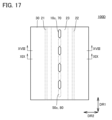
- FIG. 17 is a plan view of printed wiring board 100D.
- 18 is a cross-sectional view taken along line XVIII-XVIII of FIG. 17.
- FIG. 19 is a cross-sectional view taken along line XIX-XIX in FIG. 17.
- FIG. 20 is a plan view of a printed wiring board (100D) according to a modification.
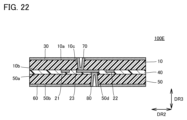
- FIG. 21 is a plan view of printed wiring board 100E.
- 22 is a cross-sectional view along XXII-XXII in FIG. 21.
- FIG. 23 is a cross-sectional view along XXIII-XXIII of FIG. 21.
- FIG. 24 is a plan view of printed wiring board 100F.
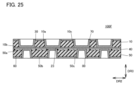
- 25 is a cross-sectional view along XXV-XXV of FIG. 24.
- FIG. 26 is a cross-sectional view along XXVI-XXVI in FIG. 24.
- the present disclosure has been made in view of the problems of the prior art as described above. More specifically, the present disclosure provides a printed wiring board capable of suppressing crosstalk between the first wiring pattern and the second wiring pattern.
- a printed wiring board includes a first insulating layer having a first main surface and a second main surface opposite to the first main surface, a first insulating layer disposed on the second main surface, and , a first wiring pattern, a second wiring pattern, and a first ground pattern extending along the first direction in plan view, a second ground pattern disposed on the first main surface, and the first wiring An adhesive layer arranged on the second main surface so as to cover the pattern, the second wiring pattern and the first ground pattern, and a third main surface arranged on the adhesive layer and facing the adhesive layer.
- the first ground pattern is between the first wiring pattern and the second wiring pattern in a second direction orthogonal to the first direction and is separated from the first wiring pattern and the second wiring pattern.
- the ground pattern penetrates the first insulating layer and the second ground pattern in a thickness direction perpendicular to the first direction and the second direction, and is the same as the first ground pattern in plan view.
- a plurality of overlapping first through holes are formed. The plurality of first through-holes are arranged at intervals so as to form a row along the first direction.
- a plurality of third ground patterns that penetrate the adhesive layer, the second insulating layer and the third ground pattern in the thickness direction and overlap the first ground pattern in a plan view.
- 2 through holes are formed.
- the plurality of second through-holes are arranged at intervals so as to form a row along the first direction.
- the first conductor layer is arranged on the inner wall surface of each of the plurality of first through holes and electrically connected to the first ground pattern and the second ground pattern.
- the second conductor layer is arranged on the inner wall surface of each of the plurality of second through holes and electrically connected to the first ground pattern and the third ground pattern.
- Each of the plurality of first through holes and each of the plurality of second through holes has a width in the first direction greater than the width in the second direction.
- each of the plurality of first through holes and each of the plurality of second through holes may extend along the first direction in plan view.
- the first insulating layer and the second ground pattern penetrate through the first insulating layer and the second ground pattern in the thickness direction, and the first ground pattern in plan view
- a plurality of third through-holes may be further formed to overlap with each other.
- the plurality of third through holes may be arranged at intervals so as to form a row along the first direction between the row of the plurality of first through holes and the second wiring pattern.
- the adhesive layer, the second insulating layer and the third ground pattern there are provided a plurality of third ground patterns that penetrate the adhesive layer, the second insulating layer and the third ground pattern in the thickness direction and overlap the first ground pattern in a plan view. 4 through holes may be further formed.
- the plurality of fourth through holes may be arranged at intervals so as to form a row along the first direction between the row of the plurality of second through holes and the second wiring pattern.
- Each of the plurality of third through holes may be displaced from each of the plurality of first through holes in the first direction.
- Each of the plurality of fourth through holes may be displaced from each of the plurality of second through holes in the first direction.
- the first conductor layer may be further arranged on the inner wall surface of each of the plurality of third through holes and electrically connected to the first ground pattern and the second ground pattern.
- the second conductor layer may be further arranged on the inner wall surface of each of the plurality of fourth through holes and electrically connected to the first ground pattern and the third ground pattern.
- Each of the plurality of third through holes and each of the plurality of fourth through holes may have a width in the first direction greater than a width in the second direction.
- each of the plurality of first through holes, each of the plurality of second through holes, each of the plurality of third through holes, and each of the plurality of fourth through holes In plan view, it may extend along the first direction.
- each of the plurality of first through holes, each of the plurality of second through holes, each of the plurality of third through holes, and each of the plurality of fourth through holes In plan view, it may have a first portion extending along the first direction and a second portion connected to a central portion of the first portion in the first direction.
- the second portion In each of the plurality of first through holes and each of the plurality of second through holes, the second portion extends from the first portion along the direction from the first wiring pattern side to the second wiring pattern side.
- the second portion extends from the first portion along the direction from the second wiring pattern side to the first wiring pattern side.
- each of the plurality of first through holes, each of the plurality of second through holes, each of the plurality of third through holes, and each of the plurality of fourth through holes Planar view WHEREIN: You may have the 3rd part and 4th part which extend linearly.
- One end of the third portion and one end of the fourth portion may be connected to each other.
- the one end of the third portion may be located on the one side in the first direction with respect to the other end of the third portion.
- the one end of the fourth portion may be on the other side in the first direction than the other end of the fourth portion.
- the other end of the third portion and the other end of the fourth portion are located further than the one end of the third portion and the one end of the fourth portion, respectively. It may be on the second wiring pattern side.
- the other end of the third portion and the other end of the fourth portion are positioned further than the one end of the third portion and the one end of the fourth portion, respectively. It may be on the side of the first wiring pattern.
- each of the plurality of first through holes and each of the plurality of second through holes may extend along the first direction in plan view.
- a position in the second direction of each of the plurality of first through holes may overlap a position in the second direction of each of the plurality of second through holes.
- Each of the plurality of first through holes may be between two of the plurality of adjacent second through holes in the first direction.
- the first insulating layer and the second ground pattern penetrate through the first insulating layer and the second ground pattern in the thickness direction, and the first ground pattern in plan view
- a plurality of third through-holes may be further formed to overlap with each other.
- the plurality of third through holes may be arranged at intervals so as to form a row along the first direction between the row of the plurality of first through holes and the second wiring pattern.
- the adhesive layer, the second insulating layer, and the third ground pattern have a plurality of fourth through holes that penetrate the second insulating layer and the adhesive layer in the thickness direction and overlap the first ground pattern in plan view. Further, it may be formed.
- the plurality of fourth through holes may be arranged at intervals so as to form a row along the first direction between the row of the plurality of second through holes and the second wiring pattern.
- Each of the plurality of third through holes and each of the plurality of fourth through holes may extend along the first direction in plan view.
- a position in the second direction of each of the plurality of third through holes may overlap a position in the second direction of each of the plurality of fourth through holes.
- Each of the plurality of third through holes may be between two of the plurality of adjacent fourth through holes in the first direction.
- the first conductor layer may be further arranged on the inner wall surface of each of the plurality of third through holes and electrically connected to the first ground pattern and the second ground pattern.
- the second conductor layer may be further arranged on the inner wall surface of each of the plurality of fourth through holes and electrically connected to the first ground pattern and the third ground pattern.
- the first ground pattern exposed from the first through hole, the first ground pattern exposed from the second through hole, and the first ground pattern exposed from the third through hole Damage to the first ground pattern exposed from the ground pattern and the fourth through hole can be suppressed.
- each of the plurality of third through holes may be displaced from each of the plurality of first through holes in the first direction.
- Each of the plurality of fourth through holes may be displaced from each of the plurality of second through holes in the first direction.
- each of the plurality of first through holes and each of the plurality of second through holes may extend along the first direction in plan view.
- a position of each of the plurality of first through holes may overlap a position of each of the plurality of second through holes in the first direction and the second direction.
- the length in the first direction of each of the plurality of first through holes may be greater than the length in the first direction of the plurality of second through holes.
- the first insulating layer and the second ground pattern penetrate through the first insulating layer and the second ground pattern in the thickness direction, and in plan view, the first ground pattern
- a plurality of overlapping third through holes may be further formed.
- the plurality of third through holes may be arranged at intervals so as to form a row along the first direction between the row of the plurality of first through holes and the second wiring pattern.
- the plurality of fourth through holes may be arranged at intervals so as to form a row along the first direction between the row of the plurality of second through holes and the second wiring pattern.
- Each of the plurality of third through holes and each of the plurality of fourth through holes may extend along the first direction in plan view.
- a position of each of the plurality of third through holes may overlap a position of each of the plurality of fourth through holes in the first direction and the second direction.
- a length in the first direction of each of the plurality of fourth through holes may be greater than a length in the first direction of the plurality of third through holes.
- the first conductor layer may be further arranged on the inner wall surface of each of the plurality of third through holes and electrically connected to the first ground pattern and the second ground pattern.
- the second conductor layer may be further arranged on the inner wall surface of each of the plurality of fourth through holes and electrically connected to the first ground pattern and the third ground pattern.
- the first ground pattern exposed from the first through hole and the second through hole and the first ground pattern exposed from the third through hole and the fourth through hole are damaged. can be suppressed.
- a printed wiring board according to the first embodiment will be described.
- the printed wiring board according to the first embodiment is referred to as printed wiring board 100 .
- FIG. 1 is a plan view of the printed wiring board 100.
- FIG. FIG. 2 is a cross-sectional view along II-II in FIG.
- printed wiring board 100 includes first insulating layer 10, first wiring pattern 21, second wiring pattern 22 and first ground pattern 23, and second ground pattern 30. , an adhesive layer 40 , a second insulating layer 50 , a third ground pattern 60 , a first conductor layer 70 and a second conductor layer 80 .
- the first insulating layer 10 is made of an electrically insulating material.
- the first insulating layer 10 is made of, for example, polyimide, fluorine resin, or the like.
- the first insulating layer 10 has a first major surface 10a and a second major surface 10b.
- the first main surface 10a and the second main surface 10b are end surfaces in the thickness direction of the first insulating layer 10 .
- the second principal surface 10b is the opposite surface of the first principal surface 10a.
- the first wiring pattern 21, the second wiring pattern 22 and the first ground pattern 23 are arranged on the second main surface 10b.
- the first wiring pattern 21, the second wiring pattern 22 and the first ground pattern 23 are made of an electrically conductive material.
- the first wiring pattern 21, the second wiring pattern 22 and the first ground pattern 23 are made of copper, for example.
- the first wiring pattern 21, the second wiring pattern 22, and the first ground pattern 23 extend along the first direction DR1 in plan view.
- the first ground pattern 23 is between the first wiring pattern 21 and the second wiring pattern 22 and is separated from the first wiring pattern 21 and the second wiring pattern 22 in the second direction DR2.
- the second direction DR2 is a direction orthogonal to the first direction DR1.
- the width of the first ground pattern 23 in the second direction DR2 is preferably larger than the width of the first wiring pattern 21 in the second direction DR2 and the width of the second wiring pattern 22 in the second direction DR2.
- the second ground pattern 30 is made of an electrically conductive material.
- the second ground pattern 30 is made of copper, for example.
- the second ground pattern 30 is arranged on the first main surface 10a.
- the second ground pattern 30 overlaps the first wiring pattern 21, the second wiring pattern 22 and the first ground pattern 23 in plan view.
- the second ground pattern 30 preferably covers the entire first main surface 10a.
- the adhesive layer 40 is made of, for example, a thermosetting resin material such as epoxy resin.
- the adhesive layer 40 is arranged on the second main surface 10 b so as to cover the first wiring pattern 21 , the second wiring pattern 22 and the first ground pattern 23 .
- the second insulating layer 50 is made of an electrically insulating material.
- the second insulating layer 50 is made of, for example, polyimide, fluorine resin, or the like.
- the second insulating layer 50 is preferably made of the same material as the first insulating layer 10 .
- the second insulating layer 50 has a third main surface 50a and a fourth main surface 50b.
- the third main surface 50a and the fourth main surface 50b are end surfaces in the thickness direction of the second insulating layer 50 .
- the third main surface 50a faces the adhesive layer 40 side.
- the fourth principal surface 50b is the opposite surface of the third principal surface 50a.
- the third ground pattern 60 is made of an electrically conductive material.
- the third ground pattern 60 is made of copper, for example.
- the third ground pattern 60 is arranged on the fourth main surface 50b.
- the third ground pattern 60 overlaps the first wiring pattern 21, the second wiring pattern 22 and the first ground pattern 23 in plan view.
- the third ground pattern 60 preferably covers the entire fourth main surface 50b.
- the first insulating layer 10 and the second ground pattern 30 are formed with a plurality of first through holes 10c.
- the first through hole 10c penetrates the first insulating layer 10 and the second ground pattern 30 in the thickness direction DR3.
- a thickness direction DR3 is a direction orthogonal to the first direction DR1 and the second direction DR2.
- the plurality of first through holes 10c are arranged in a row along the first direction DR1 at intervals in plan view.
- the interval between the first through holes 10c adjacent in the first direction DR1 is constant, for example.
- the first through hole 10c overlaps the first ground pattern 23 in plan view. That is, the first ground pattern 23 is exposed from the first through hole 10c.
- the width of the first through hole 10c in the first direction DR1 is greater than the width of the first through hole 10c in the second direction DR2.
- the first through hole 10c extends, for example, along the first direction DR1.
- the first through hole 10c preferably has an oval shape whose longitudinal direction is along the first direction DR1 in plan view.
- a plurality of second through holes 50 c are formed in the adhesive layer 40 , the second insulating layer 50 and the third ground pattern 60 .
- the second through hole 50c penetrates the adhesive layer 40, the second insulating layer 50 and the third ground pattern 60 in the thickness direction DR3.
- the plurality of second through holes 50c are arranged in a row along the first direction DR1 at intervals in plan view.
- the interval between the second through holes 50c adjacent in the first direction DR1 is constant, for example.
- the second through hole 50c overlaps the first ground pattern 23 in plan view. That is, the first ground pattern 23 is exposed from the second through hole 50c.
- the width of the second through hole 50c in the first direction DR1 is greater than the width of the second through hole 50c in the second direction DR2.
- the second through hole 50c extends, for example, along the first direction DR1.
- the second through hole 50c preferably has an oval shape whose longitudinal direction is along the first direction DR1 in plan view.
- the width of the first through hole 10c in the first direction DR1 is equal to the width of the second through hole 50c in the first direction DR1
- the width of the first through hole 10c in the second direction DR2 is the second direction of the second through hole 50c. Equal to the width in DR2.
- the position in the first direction DR1 and the position in the second direction DR2 of the first through hole 10c overlap the position in the first direction DR1 and the position in the second direction DR2 of the second through hole 50c, respectively.
- the first conductor layer 70 is, for example, a layer formed by plating.
- the first conductor layer 70 is made of copper, for example.
- the first conductor layer 70 is arranged on the inner wall surface of the first through hole 10c.
- the first conductor layer 70 may also be arranged on the first ground pattern 23 exposed from the first through hole 10c.
- the first ground pattern 23 exposed from the first through hole 10 c is electrically connected to the second ground pattern 30 by the first conductor layer 70 .
- the second conductor layer 80 is, for example, a layer formed by plating.
- the second conductor layer 80 is made of copper, for example.
- the second conductor layer 80 is arranged on the inner wall surface of the second through hole 50c.
- the second conductor layer 80 may also be arranged on the first ground pattern 23 exposed from the second through hole 50c.
- the first ground pattern 23 exposed from the second through hole 50 c is electrically connected to the third ground pattern 60 by the second conductor layer 80 .
- FIG. 3 is a process diagram showing a method for manufacturing the printed wiring board 100.
- the method for manufacturing printed wiring board 100 includes preparation step S1, patterning step S2, bonding step S3, through-hole forming step S4, and plating step S5. .
- FIG. 4 is a cross-sectional view explaining the preparation step S1.
- the first insulating layer 10 is prepared in the preparation step S1.
- a copper foil 31 and a copper foil 24 are respectively arranged on the first main surface 10a and the second main surface 10b of the first insulating layer 10 prepared in the preparation step S1. Note that the copper foil 31 becomes the second ground pattern 30 .
- FIG. 5 is a cross-sectional view explaining the patterning step S2. As shown in FIG. 5, in the patterning step S2, the copper foil 24 is patterned to form the first wiring pattern 21, the second wiring pattern 22 and the first ground pattern 23. As shown in FIG. 5, in the patterning step S2, the copper foil 24 is patterned to form the first wiring pattern 21, the second wiring pattern 22 and the first ground pattern 23. As shown in FIG. 5, in the patterning step S2, the copper foil 24 is patterned to form the first wiring pattern 21, the second wiring pattern 22 and the first ground pattern 23. As shown in FIG.
- the copper foil 24 In the patterning of the copper foil 24, first, for example, a dry film resist is attached on the copper foil 24. Second, the applied dry film resist is developed and exposed. Thirdly, the first wiring pattern 21, the second wiring pattern 22 and the first ground pattern 23 are formed by etching the copper foil 24 using the developed and exposed dry film resist as a mask.
- FIG. 6 is a cross-sectional view for explaining the bonding step S3.
- the second insulating layer 50 having the copper foil 61 disposed on the fourth main surface 50b is attached to the first insulating layer 10 using the adhesive layer 40. be.
- the copper foil 61 becomes the third ground pattern 60 .
- FIG. 7 is a cross-sectional view for explaining the through-hole forming step S4.
- the first through-hole 10c and the second through-hole 50c are formed. Formation of the first through-hole 10c and formation of the second through-hole 50c are performed, for example, by irradiating laser light.
- plating step S5 plating is performed to form the first conductor layer 70 on the inner wall surface of the first through hole 10c and on the first ground pattern 23 exposed from the first through hole 10c, A second conductor layer 80 is formed on the inner wall surface of the second through hole 50c and on the first ground pattern 23 exposed from the second through hole 50c.
- This plating is performed by an electroless plating method or an electrolytic plating method.
- the printed wiring board 100 having the structure shown in FIGS. 1 and 2 is manufactured.
- printed wiring board 100 The effect of printed wiring board 100 will be described below in comparison with a printed wiring board according to a comparative example.
- a printed wiring board according to the comparative example is referred to as printed wiring board 200 .
- FIG. 8 is a plan view of the printed wiring board 200.
- FIG. 9 is a cross-sectional view taken along line IX-IX in FIG. 8.
- printed wiring board 200 includes first insulating layer 10, first wiring pattern 21, second wiring pattern 22 and first ground pattern 23, and second ground pattern 30. , an adhesive layer 40 , a second insulating layer 50 , a third ground pattern 60 , a first conductor layer 70 and a second conductor layer 80 .
- the first through holes 10c and the second through holes 50c are circular in plan view. That is, in printed wiring board 200, the width of first through hole 10c in second direction DR2 and the width of second through hole 50c in second direction DR2 are respectively the width of first through hole 10c in first direction DR1 and It is equal to the width in the first direction DR1 of the second through hole 50c.
- the first wiring pattern 21 and the second wiring pattern 22 When signals are transmitted through the first wiring pattern 21 and the second wiring pattern 22 (when current flows through the first wiring pattern 21 and the second wiring pattern 22), the first wiring pattern 21 and the second wiring pattern 22 emits electromagnetic waves.
- the electromagnetic wave radiated from the first wiring pattern 21 becomes noise for the signal transmitted through the second wiring pattern 22, and the electromagnetic wave radiated from the second wiring pattern 22 becomes noise for the signal transmitted through the first wiring pattern 21. . That is, crosstalk occurs between the first wiring pattern 21 and the second wiring pattern 22 .
- the first conductor layer 70 electrically connects the first ground pattern 23 and the second ground pattern 30 .
- the second conductor layer 80 electrically connects the first ground pattern 23 and the third ground pattern 60 . Therefore, in the printed wiring board 200 , part of the electromagnetic waves radiated from the first wiring pattern 21 and directed to the second wiring pattern 22 and part of the electromagnetic waves radiated from the second wiring pattern 22 and directed to the first wiring pattern 21 A portion is shielded by the first conductor layer 70 and the second conductor layer 80 .
- the above electromagnetic waves may pass through between two adjacent first through holes 10c and between two adjacent second through holes 50c. Therefore, it is effective for shielding electromagnetic waves by the first conductor layer 70 and the second conductor layer 80 to form the first through holes 10c and the second through holes 50c densely in the first direction DR1.
- the first through holes 10c and the second through holes 50c are circular in plan view. , the distance between adjacent first through holes 10c and the distance between two adjacent second through holes 50c need to be reduced. However, from the viewpoint of processing accuracy of the first through-holes 10c and the second through-holes 50c, there is a limit to reducing the interval between the adjacent first through-holes 10c.
- the width of first through hole 10c in first direction DR1 and the width of second through hole 50c in first direction DR1 are respectively the width of first through hole 10c in second direction DR2 and the width of second through hole 50c in second direction DR2. Since it is larger than the width in the second direction DR2 of the two through-holes 50c, the interval between two adjacent first through-holes 10c and the interval between two adjacent second through-holes 50c are reduced.
- the first through holes 10c and the second through holes 50c can be formed densely in the first direction DR1.
- crosstalk between first wiring pattern 21 and second wiring pattern 22 is further suppressed as compared with printed wiring board 200 .
- a printed wiring board according to the second embodiment will be described.
- a printed wiring board according to the second embodiment is referred to as a printed wiring board 100A.
- points different from printed wiring board 100 will be mainly described, and redundant description will not be repeated.
- FIG. 10 is a plan view of the printed wiring board 100A.
- 11 is a cross-sectional view along XI-XI in FIG. 12 is a cross-sectional view taken along line XII-XII in FIG. 10.
- FIG. 10A includes first insulating layer 10, first wiring pattern 21, second wiring pattern 22 and first ground pattern 23, and second ground pattern. 30 , an adhesive layer 40 , a second insulating layer 50 , a third ground pattern 60 , a first conductor layer 70 and a second conductor layer 80 .
- the configuration of printed wiring board 100A is common to the configuration of printed wiring board 100 .
- a plurality of third through holes 10d are formed in the first insulating layer 10 and the second ground pattern 30 in the printed wiring board 100A.
- the third through hole 10d penetrates the first insulating layer 10 and the second ground pattern 30 in the thickness direction DR3.
- the third through hole 10d overlaps the first ground pattern 23 in plan view. That is, the first ground pattern 23 is exposed from the third through hole 10d.
- the plurality of third through holes 10d are arranged at intervals so as to form a row along the first direction DR1.
- the interval between two adjacent third through holes 10d is constant, for example.
- the row of the third through holes 10d is arranged between the row of the first through holes 10c and the second wiring pattern 22 in plan view.
- the position of the third through hole 10d in the first direction DR1 is shifted from the position of the first through hole 10c in the first direction DR1.
- the width of the third through hole 10d in the first direction DR1 is greater than the width of the third through hole 10d in the second direction DR2.
- the third through hole 10d extends, for example, along the first direction DR1.
- the third through hole 10d preferably has an oval shape whose longitudinal direction is along the first direction DR1 in plan view.
- a plurality of fourth through holes 50d are formed in the adhesive layer 40, the second insulating layer 50 and the third ground pattern 60 in the printed wiring board 100A.
- the fourth through hole 50d penetrates the adhesive layer 40, the second insulating layer 50 and the third ground pattern 60 in the thickness direction DR3.
- the fourth through hole 50d overlaps the first ground pattern 23 in plan view. That is, the first ground pattern 23 is exposed from the fourth through hole 50d.
- the plurality of fourth through holes 50d are arranged at intervals so as to form a row along the first direction DR1.
- the interval between two adjacent fourth through holes 50d is constant, for example.
- the row of the fourth through holes 50d is arranged between the row of the second through holes 50c and the second wiring pattern 22 in plan view.
- the position of the fourth through hole 50d in the first direction DR1 is shifted from the position of the second through hole 50c in the first direction DR1.
- the width of the fourth through hole 50d in the first direction DR1 is greater than the width of the fourth through hole 50d in the second direction DR2.
- the fourth through hole 50d extends, for example, along the first direction DR1.
- the fourth through hole 50d preferably has an oval shape whose longitudinal direction is along the first direction DR1 in plan view.
- the position of the third through hole 10d in the first direction DR1 and the position in the second direction DR2 respectively overlap the position of the fourth through hole 50d in the first direction DR1 and the position in the second direction DR2.
- the first conductor layer 70 is also arranged on the inner wall surface of the third through hole 10d.
- the first conductor layer 70 may also be arranged on the first ground pattern 23 exposed from the third through hole 10d.
- second conductor layer 80 is also arranged on the inner wall surface of fourth through hole 50d.
- the second conductor layer 80 may also be arranged on the first ground pattern 23 exposed from the fourth through hole 50d.
- the first ground pattern 23 exposed from the third through hole 10 d is electrically connected to the second ground pattern 30 by the first conductor layer 70 .
- the second conductor layer 80 electrically connects the first ground pattern 23 exposed from the fourth through hole 50 d to the third ground pattern 60 .
- the configuration of printed wiring board 100A differs from that of printed wiring board 100 in these respects.
- the method for manufacturing the printed wiring board 100A includes a preparation step S1, a patterning step S2, a bonding step S3, a through-hole forming step S4, and a plating step S5.
- the method for manufacturing printed wiring board 100A is common to the method for manufacturing printed wiring board 100.
- the third through-hole 10d and the fourth through-hole 50d are formed in addition to the first through-hole 10c and the second through-hole 50c.
- the first conductor layer 70 is also formed on the inner wall surfaces of the third through holes 10d and on the first ground pattern 23 exposed from the third through holes 10d. be done.
- the second conductor layer 80 is also formed on the inner wall surfaces of the fourth through holes 50d and on the first ground pattern 23 exposed from the fourth through holes 50d. be done. Regarding these points, the method for manufacturing printed wiring board 100A is different from the method for manufacturing printed wiring board 100 .
- the electromagnetic wave emitted from first wiring pattern 21 and the electromagnetic wave emitted from second wiring pattern 22 pass between two adjacent first through holes 10c and between adjacent second through holes 10c. It may pass through between the holes 50c.
- the position of third through hole 10d in first direction DR1 is displaced from the position of first through hole 10c in first direction DR1, and the position of fourth through hole 50d in first direction DR1 is displaced. It is shifted from the position of the second through hole 50c in the first direction DR1.
- the electromagnetic waves radiated from first wiring pattern 21 passed between two adjacent first through holes 10c and between two adjacent second through holes 50c. However, it is blocked by the first conductor layer 70 arranged on the inner wall surface of the third through hole 10d and the second conductor layer 80 arranged on the inner wall surface of the fourth through hole 50d.
- electromagnetic waves radiated from second wiring pattern 22 pass between two adjacent third through holes 10d and between two adjacent fourth through holes 50d. Even if it is, it is blocked by the first conductor layer 70 arranged on the inner wall surface of the first through hole 10c and the second conductor layer 80 arranged on the inner wall surface of the second through hole 50c.
- crosstalk between the first wiring pattern 21 and the second wiring pattern 22 is further suppressed as compared with the printed wiring board 100 .
- a printed wiring board according to the third embodiment will be described.
- a printed wiring board according to the third embodiment is referred to as a printed wiring board 100B.
- points different from printed wiring board 100A will be mainly described, and duplicate description will not be repeated.
- FIG. 13 is a plan view of the printed wiring board 100B.
- FIG. 14 is a bottom view of printed wiring board 100B.
- the printed wiring board 100B includes a first insulating layer 10, a first wiring pattern 21, a second wiring pattern 22 and a first ground pattern 23, a second ground pattern 30, It has an adhesive layer 40 , a second insulating layer 50 , a third ground pattern 60 , a first conductor layer 70 and a second conductor layer 80 .
- the configuration of printed wiring board 100B is common to the configuration of printed wiring board 100A.
- first through hole 10c and third through hole 10d have first portion 10e and second portion 10f
- second through hole 50c and fourth through hole 50d have first portion 50e. and a second portion 50f.
- the first portion 10e and the first portion 50e extend along the first direction DR1.
- the second portion 10f and the second portion 50f extend along the second direction DR2.
- the second portion 10f and the second portion 50f are respectively connected to the central portion of the first portion 10e in the first direction DR1 and the central portion of the first portion 50e in the first direction DR1.
- the second portion 10f extends from the first portion 10e along the direction from the first wiring pattern 21 toward the second wiring pattern 22.
- the second portion 10 f extends from the first portion 10 e along the direction from the second wiring pattern 22 toward the first wiring pattern 21 .
- the second portion 50f extends from the first portion 50e along the direction from the first wiring pattern 21 toward the second wiring pattern 22.
- the second portion 50 f extends from the first portion 50 e along the direction from the second wiring pattern 22 toward the first wiring pattern 21 .
- the configuration of printed wiring board 100B is different from that of printed wiring board 100A.
- the method for manufacturing the printed wiring board 100B includes a preparation step S1, a patterning step S2, a bonding step S3, a through-hole forming step S4, and a plating step S5.
- the method for manufacturing printed wiring board 100B is common to the method for manufacturing printed wiring board 100A.
- first through-hole 10c, second through-hole 50c, third through-hole 10d, and fourth through-hole 50d formed in through-hole forming step S4 are the same as those of printed wiring board 100A. It is different from the manufacturing method.
- the electromagnetic waves radiated from the first wiring pattern 21 and the electromagnetic waves radiated from the second wiring pattern 22 pass between two adjacent first through holes 10c and between two adjacent second through holes 10c. It passes through between two through holes 50c, between two adjacent third through holes 10d, and between two adjacent fourth through holes 50d along a direction inclined with respect to the second direction DR2.
- the electromagnetic waves radiated from the first wiring pattern 21 and the electromagnetic waves radiated from the second wiring pattern 22 pass between two adjacent first through holes 10c and between two adjacent second through holes 10c. It passes through between two through holes 50c, between two adjacent third through holes 10d, and between two adjacent fourth through holes 50d along a direction inclined with respect to the second direction DR2.
- third through hole 10d has second portion 10f and fourth through hole 50d has second portion 50f. , even if it passes between two adjacent first through-holes 10c and between adjacent second through-holes 50c, the first It is likely to be blocked by the conductor layer 70 and the second conductor layer 80 on the inner wall surface of the fourth through hole 50d in the second portion 50f.
- first through hole 10c has second portion 10f and second through hole 50c has second portion 50f. Even if the electromagnetic wave passes between the two adjacent third through holes 10d and between the adjacent fourth through holes 50d, it does not reach the inner wall surface of the first through hole 10c in the second portion 10f. and the second conductor layer 80 on the inner wall surface of the second through hole 50c in the second portion 50f.
- crosstalk between the first wiring pattern 21 and the second wiring pattern 22 is further suppressed as compared with the printed wiring board 100A.
- a printed wiring board according to the fourth embodiment will be described.
- a printed wiring board according to the fourth embodiment is referred to as a printed wiring board 100C.
- points different from printed wiring board 100A will be mainly described, and duplicate description will not be repeated.
- FIG. 15 is a plan view of the printed wiring board 100C.
- FIG. 16 is a bottom view of printed wiring board 100C.
- the printed wiring board 100C includes a first insulating layer 10, a first wiring pattern 21, a second wiring pattern 22, a first ground pattern 23, a second ground pattern 30, It has an adhesive layer 40 , a second insulating layer 50 , a third ground pattern 60 , a first conductor layer 70 and a second conductor layer 80 .
- the configuration of printed wiring board 100C is common to the configuration of printed wiring board 100A.
- the first through hole 10c and the third through hole 10d have a third portion 10g and a fourth portion 10h extending linearly in plan view.
- the second through hole 50c and the fourth through hole 50d have a third portion 50g and a fourth portion 50h extending linearly in plan view.
- One end of the third portion 10g and one end of the fourth portion 10h are connected to each other.
- One end of the third portion 10g is on one side in the first direction DR1 relative to the other end of the third portion 10g.
- One end of the fourth portion 10h is on the other side in the first direction DR1 than the other end of the fourth portion 10h.
- One end of the third portion 50g and one end of the fourth portion 50h are connected to each other.
- One end of the third portion 50g is on one side in the first direction DR1 relative to the other end of the third portion 50g.
- One end of the fourth portion 50h is on the other side in the first direction DR1 of the other end of the fourth portion 50h.
- the other end of the third portion 10g and the other end of the fourth portion 10h are closer to the second wiring pattern 22 than the one end of the third portion 10g and the one end of the fourth portion 10h, respectively. be.
- the third through hole 10d the other end of the third portion 10g and the other end of the fourth portion 10h are closer to the first wiring pattern 21 than the one end of the third portion 10g and the one end of the fourth portion 10h, respectively. be. That is, the first through hole 10c and the third through hole 10d are L-shaped in plan view.
- the other end of the third portion 50g and the other end of the fourth portion 50h are closer to the second wiring pattern 22 than the one end of the third portion 50g and the one end of the fourth portion 50h, respectively. be.
- the fourth through hole 50d the other end of the third portion 50g and the other end of the fourth portion 50h are closer to the first wiring pattern 21 than the one end of the third portion 50g and the one end of the fourth portion 50h, respectively. be. That is, the second through hole 50c and the fourth through hole 50d are L-shaped in plan view. In these respects, the configuration of printed wiring board 100C differs from that of printed wiring board 100A.
- the method for manufacturing the printed wiring board 100C includes a preparation step S1, a patterning step S2, a bonding step S3, a through-hole forming step S4, and a plating step S5.
- the method for manufacturing printed wiring board 100C is common to the method for manufacturing printed wiring board 100B.
- first through-hole 10c, second through-hole 50c, third through-hole 10d, and fourth through-hole 50d formed in through-hole forming step S4 are the same as those of printed wiring board 100A. It is different from the manufacturing method.
- the electromagnetic waves radiated from the first wiring pattern 21 and the electromagnetic waves radiated from the second wiring pattern 22 pass between two adjacent first through holes 10c and between two adjacent second through holes 10c. It passes through between two through holes 50c, between two adjacent third through holes 10d, and between two adjacent fourth through holes 50d along a direction inclined with respect to the second direction DR2.
- the electromagnetic waves radiated from the first wiring pattern 21 and the electromagnetic waves radiated from the second wiring pattern 22 pass between two adjacent first through holes 10c and between two adjacent second through holes 10c. It passes through between two through holes 50c, between two adjacent third through holes 10d, and between two adjacent fourth through holes 50d along a direction inclined with respect to the second direction DR2.
- third through hole 10d has third portion 10g and fourth portion 10h
- fourth through hole 50d has third portion 50g and fourth portion 50h. Even if an electromagnetic wave radiated from one wiring pattern 21 passes between two adjacent first through holes 10c and between adjacent second through holes 50c, the inner wall surface of the third through hole 10d It is easily blocked by the upper first conductor layer 70 and the second conductor layer 80 on the inner wall surface of the fourth through hole 50d.
- first through hole 10c has third portion 10g and fourth portion 10h
- second through hole 50c has third portion 50g and fourth portion 50h. Therefore, even if the electromagnetic wave radiated from the second wiring pattern 22 passes between the two adjacent third through holes 10d and between the adjacent fourth through holes 50d, and the second conductor layer 80 on the inner wall surface of the second through-hole 50c.
- crosstalk between the first wiring pattern 21 and the second wiring pattern 22 is further suppressed as compared with the printed wiring board 100A.
- a printed wiring board according to the fifth embodiment will be described.
- the printed wiring board according to the fifth embodiment is referred to as printed wiring board 100D.
- points different from printed wiring board 100 will be mainly described, and redundant description will not be repeated.
- FIG. 17 is a plan view of the printed wiring board 100D.
- 18 is a cross-sectional view taken along line XVIII-XVIII of FIG. 17.
- FIG. 19 is a cross-sectional view taken along line XIX-XIX in FIG. 17.
- printed wiring board 100D includes first insulating layer 10, first wiring pattern 21, second wiring pattern 22, first ground pattern 23, and second ground pattern. 30 , an adhesive layer 40 , a second insulating layer 50 , a third ground pattern 60 , a first conductor layer 70 and a second conductor layer 80 .
- the configuration of printed wiring board (100D) is common to the configuration of printed wiring board (100).
- first through hole 10c is between two adjacent second through holes 50c in first direction DR1. It differs from the 100 configuration.
- the method for manufacturing the printed wiring board 100D includes a preparation step S1, a patterning step S2, a bonding step S3, a through-hole forming step S4, and a plating step S5.
- the method for manufacturing printed wiring board (100D) is common to the method for manufacturing printed wiring board (100).
- the method for manufacturing printed wiring board 100D differs from the method for manufacturing printed wiring board 100 in the position of second through hole 50c formed in through hole forming step S4.
- first ground pattern 23 is exposed from both the first through hole 10c and the second through hole 50c. Therefore, in printed wiring board 100 , first ground pattern 23 may be damaged.
- the first ground pattern 23 is exposed only from either the first through hole 10c or the second through hole 50c.
- first ground pattern 23 exposed from first through hole 10c is supported by adhesive layer 40, second insulating layer 50 and third ground pattern 60.
- the first ground pattern 23 exposed from the second through hole 50 c is supported by the first insulating layer 10 and the second ground pattern 30 . Therefore, in printed wiring board 100 ⁇ /b>D, damage to first ground pattern 23 can be suppressed as compared with printed wiring board 100 .
- FIG. 20 is a plan view of a printed wiring board (100D) according to a modification.
- first through hole 10c and second through hole 50c are circular in plan view. That is, in the printed wiring board 100D, the width in the first direction DR1 and the width in the second direction DR2 of the first through hole 10c may be equal to each other, and the width in the first direction DR1 and the width in the second direction DR2 of the second through hole 50c may be equal to each other. The widths in the two directions DR2 may be equal to each other.
- FIG. 100E A printed wiring board according to the sixth embodiment will be described.
- the printed wiring board according to the sixth embodiment is referred to as printed wiring board 100E.
- points different from printed wiring board 100A will be mainly described, and duplicate description will not be repeated.
- FIG. 21 is a plan view of printed wiring board 100E.
- 22 is a cross-sectional view along XXII-XXII in FIG. 21.
- FIG. 23 is a cross-sectional view along XXIII-XXIII of FIG. 21.
- printed wiring board 100E includes first insulating layer 10, first wiring pattern 21, second wiring pattern 22, first ground pattern 23, and second ground pattern. 30 , an adhesive layer 40 , a second insulating layer 50 , a third ground pattern 60 , a first conductor layer 70 and a second conductor layer 80 .
- the configuration of printed wiring board 100E is common to the configuration of printed wiring board 100A.
- first through-hole 10c is located between two adjacent second through-holes 50c in first direction DR1
- third through-hole 10d is located between two adjacent second through-holes 50c in first direction DR1. between two fourth through holes 50d.
- the configuration of printed wiring board 100E is common to the configuration of printed wiring board 100A.
- the method for manufacturing the printed wiring board 100E includes a preparation step S1, a patterning step S2, a bonding step S3, a through-hole forming step S4, and a plating step S5.
- the method for manufacturing printed wiring board 100E is common to the method for manufacturing printed wiring board 100A.
- the method for manufacturing printed wiring board 100E differs from the method for manufacturing printed wiring board 100A in the positions of second through-hole 50c and fourth through-hole 50d formed in through-hole forming step S4.
- first ground pattern 23 is exposed from both first through hole 10c and second through hole 50c, and is exposed from both third through hole 10d and fourth through hole 50d. there is Therefore, in printed wiring board 100A, first ground pattern 23 may be damaged.
- first ground pattern 23 is exposed only from either first through hole 10c or second through hole 50c or from third through hole 10d or fourth through hole 50d. do not have.
- first ground pattern 23 exposed from first through-hole 10c or third through-hole 10d consists of adhesive layer 40, second insulating layer 50 and third ground pattern 23.
- the first ground pattern 23 supported by the ground pattern 60 and exposed from the second through hole 50 c or the fourth through hole 50 d is supported by the first insulating layer 10 and the second ground pattern 30 . Therefore, in printed wiring board 100E, damage to first ground pattern 23 can be suppressed as compared with printed wiring board 100A.
- a printed wiring board according to the seventh embodiment will be described.
- a printed wiring board according to the seventh embodiment is referred to as a printed wiring board 100F.
- points different from printed wiring board 100A will be mainly described, and duplicate description will not be repeated.
- FIG. 24 is a plan view of the printed wiring board 100F.
- 25 is a cross-sectional view along XXV-XXV of FIG. 24.
- FIG. 26 is a cross-sectional view along XXVI-XXVI in FIG. 24.
- printed wiring board 100F includes first insulating layer 10, first wiring pattern 21, second wiring pattern 22, first ground pattern 23, and second ground pattern. 30 , an adhesive layer 40 , a second insulating layer 50 , a third ground pattern 60 , a first conductor layer 70 and a second conductor layer 80 .
- the configuration of printed wiring board 100F is common to the configuration of printed wiring board 100A.
- the width of the first through hole 10c in the first direction DR1 and the width of the second through hole 50c in the first direction DR1 are different from each other. More specifically, the width of first through hole 10c in first direction DR1 is greater than the width of second through hole 50c in first direction DR1.
- the width of the third through hole 10d in the first direction DR1 and the width of the fourth through hole 50d in the first direction DR1 are different from each other. More specifically, the width of the fourth through hole 50d in the first direction DR1 is greater than the width of the third through hole 10d in the first direction DR1. Regarding these points, the configuration of printed wiring board 100F is common to the configuration of printed wiring board 100A.
- the method for manufacturing the printed wiring board 100F includes a preparation step S1, a patterning step S2, a bonding step S3, a through-hole forming step S4, and a plating step S5.
- the method for manufacturing printed wiring board (100F) is common to the method for manufacturing printed wiring board (100A).
- the method for manufacturing printed wiring board 100F differs from the method for manufacturing printed wiring board 100A in the positions of second through-hole 50c and fourth through-hole 50d formed in through-hole forming step S4.
- first ground pattern 23 is exposed from both first through hole 10c and second through hole 50c, and is exposed from both third through hole 10d and fourth through hole 50d. there is Therefore, in printed wiring board 100A, first ground pattern 23 may be damaged.
- the first ground pattern 23 is exposed from both the first through hole 10c and the second through hole 50c, and is also exposed from both the third through hole 10d and the fourth through hole 50d.
- the area of first ground pattern 23 exposed from second through hole 50c is smaller, and the area of first ground pattern 23 exposed from third through hole 10d is smaller.
- the area of the first ground pattern 23 is reduced. Therefore, in printed wiring board 100F, damage to first ground pattern 23 can be suppressed as compared with printed wiring board 100A.
Landscapes
- Engineering & Computer Science (AREA)
- Microelectronics & Electronic Packaging (AREA)
- Manufacturing & Machinery (AREA)
- Structure Of Printed Boards (AREA)
Abstract
This printed wiring board comprises: a first insulating layer having a first main surface and a second main surface opposite the first main surface; a first wiring pattern, a second wiring pattern, and a first ground pattern that are disposed on the second main surface and extend along a first direction in a plan view; a second ground pattern disposed on the first main surface; an adhesive layer disposed on the second main surface so as to cover the first wiring pattern, the second wiring pattern, and the first ground pattern; a second insulating layer disposed on the adhesive layer and having a third main surface facing the adhesive layer side and a fourth main surface opposite the third main surface; a third ground pattern disposed on the fourth main surface; and a first conductor layer and a second conductor layer.
Description
本開示は、プリント配線板に関する。本出願は、2021年11月24日に出願した日本特許出願である特願2021-190207号に基づく優先権を主張する。当該日本特許出願に記載された全ての記載内容は、参照によって本明細書に援用される。
The present disclosure relates to printed wiring boards. This application claims priority from Japanese Patent Application No. 2021-190207 filed on November 24, 2021. All the contents described in the Japanese patent application are incorporated herein by reference.
特開2006-24618号公報(特許文献1)には、配線基板が記載されている。特許文献1に記載の配線基板は、第1誘電体層と、第1配線パターン、第2配線パターン及びコプレナグランドパターンと、第2誘電体層と、第1グランドパターン及び第2グランドパターンと、導体層とを有している。
A wiring board is described in Japanese Patent Application Laid-Open No. 2006-24618 (Patent Document 1). The wiring board described in Patent Document 1 includes a first dielectric layer, a first wiring pattern, a second wiring pattern and a coplanar ground pattern, a second dielectric layer, a first ground pattern and a second ground pattern. , and a conductor layer.
第1誘電体層は、第1主面と、第1主面の反対面である第2主面とを有している。第1配線パターン、第2配線パターン及びコプレナグランドパターンは、第2主面上に配置されている。第1配線パターン、第2配線パターン及びコプレナグランドパターンは、第1方向に沿って延在している。コプレナグランドパターンは、第1方向に直交している第2方向において、第1配線パターンと第2配線パターンとの間に配置されている。
The first dielectric layer has a first principal surface and a second principal surface opposite to the first principal surface. The first wiring pattern, the second wiring pattern and the coplanar ground pattern are arranged on the second main surface. The first wiring pattern, the second wiring pattern and the coplanar ground pattern extend along the first direction. The coplanar ground pattern is arranged between the first wiring pattern and the second wiring pattern in a second direction orthogonal to the first direction.
第2誘電体層は、第1配線パターン、第2配線パターン及びコプレナグランドパターンを覆うように第2主面上に配置されている。第2誘電体層は、第2主面側を向いている第3主面と、第3主面の反対面である第4主面とを有している。第1グランドパターン及び第2グランドパターンは、それぞれ、第1主面上及び第4主面上に配置されている。
The second dielectric layer is arranged on the second main surface so as to cover the first wiring pattern, the second wiring pattern and the coplanar ground pattern. The second dielectric layer has a third main surface facing the second main surface and a fourth main surface opposite to the third main surface. The first ground pattern and the second ground pattern are arranged on the first main surface and the fourth main surface, respectively.
特許文献1に記載の配線基板には、複数の貫通穴が形成されている。複数の貫通穴は、平面視において、第1方向に沿って並んでいる。貫通穴は、第1誘電体層、第2誘電体層及びコプレナグランドパターンを貫通している。貫通穴は、平面視において、円形である。貫通穴には、導体層が充填されている。導体層により、コプレナグランドパターンは、第1グランドパターン及び第2グランドパターンに電気的に接続されている。特許文献1に記載の配線基板では、第1配線パターンと第2配線パターンとの間のクロストークが、導体層により抑制される。
A plurality of through holes are formed in the wiring board described in Patent Document 1. The plurality of through holes are arranged along the first direction in plan view. The through hole penetrates the first dielectric layer, the second dielectric layer and the coplanar ground pattern. The through hole is circular in plan view. The through hole is filled with a conductor layer. The conductor layer electrically connects the coplanar ground pattern to the first ground pattern and the second ground pattern. In the wiring board described in Patent Document 1, crosstalk between the first wiring pattern and the second wiring pattern is suppressed by the conductor layer.
本開示のプリント配線板は、第1主面及び第1主面の反対面である第2主面を有する第1絶縁層と、第2主面上に配置されており、かつ平面視において第1方向に沿って延在している第1配線パターン、第2配線パターン及び第1グランドパターンと、第1主面上に配置されている第2グランドパターンと、第1配線パターン、第2配線パターン及び第1グランドパターンを覆うように第2主面上に配置されている接着層と、接着層上に配置されており、かつ接着層側を向いている第3主面及び第3主面の反対面である第4主面を有する第2絶縁層と、第4主面上に配置されている第3グランドパターンと、第1導体層及び第2導体層とを備える。第1グランドパターンは、第1方向に直交している第2方向において第1配線パターンと第2配線パターンとの間にあり、かつ第1配線パターン及び第2配線パターンから離間している。第1絶縁層及び第2グランドパターンには、第1方向及び第2方向に直交している厚さ方向に第1絶縁層及び第2グランドパターンを貫通し、かつ平面視において第1グランドパターンと重なっている複数の第1貫通穴が形成されている。複数の第1貫通穴は、第1方向に沿って列をなすように間隔を空けて並んでいる。接着層、第2絶縁層及び第3グランドパターンには、厚さ方向に接着層、第2絶縁層及び第3グランドパターンを貫通し、かつ平面視において第1グランドパターンと重なっている複数の第2貫通穴が形成されている。複数の第2貫通穴は、第1方向に沿って列をなすように間隔を空けて並んでいる。第1導体層は、複数の第1貫通穴の各々の内壁面上に配置され、かつ、第1グランドパターン及び第2グランドパターンに電気的に接続されている。第2導体層は、複数の第2貫通穴の各々の内壁面上に配置され、かつ第1グランドパターン及び第3グランドパターンに電気的に接続されている。複数の第1貫通穴の各々及び複数の第2貫通穴の各々は、第1方向における幅が第2方向における幅よりも大きい。
A printed wiring board of the present disclosure includes a first insulating layer having a first main surface and a second main surface opposite to the first main surface; A first wiring pattern, a second wiring pattern, and a first ground pattern extending along one direction, and a second ground pattern, the first wiring pattern, and the second wiring, which are arranged on the first main surface. An adhesive layer arranged on the second main surface so as to cover the pattern and the first ground pattern, a third main surface arranged on the adhesive layer and facing the adhesive layer, and the third main surface a second insulating layer having a fourth main surface opposite to the second insulating layer; a third ground pattern disposed on the fourth main surface; and a first conductor layer and a second conductor layer. The first ground pattern is between the first wiring pattern and the second wiring pattern in a second direction orthogonal to the first direction and is separated from the first wiring pattern and the second wiring pattern. In the first insulating layer and the second ground pattern, the ground pattern penetrates the first insulating layer and the second ground pattern in a thickness direction perpendicular to the first direction and the second direction, and is the same as the first ground pattern in plan view. A plurality of overlapping first through holes are formed. The plurality of first through-holes are arranged at intervals so as to form a row along the first direction. In the adhesive layer, the second insulating layer and the third ground pattern, there are provided a plurality of third ground patterns that penetrate the adhesive layer, the second insulating layer and the third ground pattern in the thickness direction and overlap the first ground pattern in a plan view. 2 through holes are formed. The plurality of second through-holes are arranged at intervals so as to form a row along the first direction. The first conductor layer is arranged on the inner wall surface of each of the plurality of first through holes and electrically connected to the first ground pattern and the second ground pattern. The second conductor layer is arranged on the inner wall surface of each of the plurality of second through holes and electrically connected to the first ground pattern and the third ground pattern. Each of the plurality of first through holes and each of the plurality of second through holes has a width in the first direction greater than the width in the second direction.
[本開示が解決しようとする課題]
しかしながら、特許文献1に記載の配線基板では、第1配線パターンと第2配線パターンとの間のクロストークの抑制が不十分である。 [Problems to be Solved by the Present Disclosure]
However, in the wiring board described inPatent Document 1, suppression of crosstalk between the first wiring pattern and the second wiring pattern is insufficient.
しかしながら、特許文献1に記載の配線基板では、第1配線パターンと第2配線パターンとの間のクロストークの抑制が不十分である。 [Problems to be Solved by the Present Disclosure]
However, in the wiring board described in
本開示は、上記のような従来技術の問題点に鑑みてなされたものである。より具体的には、本開示は、第1配線パターンと第2配線パターンとの間のクロストークを抑制可能なプリント配線板を提供するものである。
The present disclosure has been made in view of the problems of the prior art as described above. More specifically, the present disclosure provides a printed wiring board capable of suppressing crosstalk between the first wiring pattern and the second wiring pattern.
[本開示の効果]
本開示のプリント配線板によると、第1配線パターンと第2配線パターンとの間のクロストークを抑制可能である。 [Effect of the present disclosure]
According to the printed wiring board of the present disclosure, crosstalk between the first wiring pattern and the second wiring pattern can be suppressed.
本開示のプリント配線板によると、第1配線パターンと第2配線パターンとの間のクロストークを抑制可能である。 [Effect of the present disclosure]
According to the printed wiring board of the present disclosure, crosstalk between the first wiring pattern and the second wiring pattern can be suppressed.
[本開示の実施形態の説明]
まず、本開示の実施形態を列記して説明する。 [Description of Embodiments of the Present Disclosure]
First, embodiments of the present disclosure will be listed and described.
まず、本開示の実施形態を列記して説明する。 [Description of Embodiments of the Present Disclosure]
First, embodiments of the present disclosure will be listed and described.
(1)実施形態に係るプリント配線板は、第1主面及び第1主面の反対面である第2主面を有する第1絶縁層と、第2主面上に配置されており、かつ、平面視において第1方向に沿って延在している第1配線パターン、第2配線パターン及び第1グランドパターンと、第1主面上に配置されている第2グランドパターンと、第1配線パターン、第2配線パターン及び第1グランドパターンを覆うように第2主面上に配置されている接着層と、接着層上に配置されており、かつ接着層側を向いている第3主面及び第3主面の反対面である第4主面を有する第2絶縁層と、第4主面上に配置されている第3グランドパターンと、第1導体層及び第2導体層とを備えている。第1グランドパターンは、第1方向に直交している第2方向において第1配線パターンと第2配線パターンとの間にあり、かつ第1配線パターン及び第2配線パターンから離間している。第1絶縁層及び第2グランドパターンには、第1方向及び第2方向に直交している厚さ方向に第1絶縁層及び第2グランドパターンを貫通し、かつ平面視において第1グランドパターンと重なっている複数の第1貫通穴が形成されている。複数の第1貫通穴は、第1方向に沿って列をなすように間隔を空けて並んでいる。接着層、第2絶縁層及び第3グランドパターンには、厚さ方向に接着層、第2絶縁層及び第3グランドパターンを貫通し、かつ平面視において第1グランドパターンと重なっている複数の第2貫通穴が形成されている。複数の第2貫通穴は、第1方向に沿って列をなすように間隔を空けて並んでいる。第1導体層は、複数の第1貫通穴の各々の内壁面上に配置され、かつ第1グランドパターン及び第2グランドパターンに電気的に接続されている。第2導体層は、複数の第2貫通穴の各々の内壁面上に配置され、かつ、第1グランドパターン及び第3グランドパターンに電気的に接続されている。複数の第1貫通穴の各々及び複数の第2貫通穴の各々は、第1方向における幅が第2方向における幅よりも大きい。
(1) A printed wiring board according to an embodiment includes a first insulating layer having a first main surface and a second main surface opposite to the first main surface, a first insulating layer disposed on the second main surface, and , a first wiring pattern, a second wiring pattern, and a first ground pattern extending along the first direction in plan view, a second ground pattern disposed on the first main surface, and the first wiring An adhesive layer arranged on the second main surface so as to cover the pattern, the second wiring pattern and the first ground pattern, and a third main surface arranged on the adhesive layer and facing the adhesive layer. and a second insulating layer having a fourth principal surface opposite to the third principal surface; a third ground pattern disposed on the fourth principal surface; and a first conductor layer and a second conductor layer. ing. The first ground pattern is between the first wiring pattern and the second wiring pattern in a second direction orthogonal to the first direction and is separated from the first wiring pattern and the second wiring pattern. In the first insulating layer and the second ground pattern, the ground pattern penetrates the first insulating layer and the second ground pattern in a thickness direction perpendicular to the first direction and the second direction, and is the same as the first ground pattern in plan view. A plurality of overlapping first through holes are formed. The plurality of first through-holes are arranged at intervals so as to form a row along the first direction. In the adhesive layer, the second insulating layer and the third ground pattern, there are provided a plurality of third ground patterns that penetrate the adhesive layer, the second insulating layer and the third ground pattern in the thickness direction and overlap the first ground pattern in a plan view. 2 through holes are formed. The plurality of second through-holes are arranged at intervals so as to form a row along the first direction. The first conductor layer is arranged on the inner wall surface of each of the plurality of first through holes and electrically connected to the first ground pattern and the second ground pattern. The second conductor layer is arranged on the inner wall surface of each of the plurality of second through holes and electrically connected to the first ground pattern and the third ground pattern. Each of the plurality of first through holes and each of the plurality of second through holes has a width in the first direction greater than the width in the second direction.
上記(1)のプリント配線板によると、第1配線パターンと第2配線パターンとの間のクロストークを抑制可能である。
According to the printed wiring board of (1) above, crosstalk between the first wiring pattern and the second wiring pattern can be suppressed.
(2)上記(1)のプリント配線板では、複数の第1貫通穴の各々及び複数の第2貫通穴の各々が、平面視において、第1方向に沿って延在していてもよい。
(2) In the printed wiring board of (1) above, each of the plurality of first through holes and each of the plurality of second through holes may extend along the first direction in plan view.
(3)上記(1)のプリント配線板では、第1絶縁層及び第2グランドパターンに、厚さ方向に第1絶縁層及び第2グランドパターンを貫通し、かつ、平面視において第1グランドパターンと重なっている複数の第3貫通穴がさらに形成されていてもよい。複数の第3貫通穴は、複数の第1貫通穴の列と第2配線パターンとの間において第1方向に沿って列をなすように間隔を空けて並んでいてもよい。接着層、第2絶縁層及び第3グランドパターンには、厚さ方向に接着層、第2絶縁層及び第3グランドパターンを貫通し、かつ平面視において第1グランドパターンと重なっている複数の第4貫通穴がさらに形成されていてもよい。複数の第4貫通穴は、複数の第2貫通穴の列と第2配線パターンとの間において第1方向に沿って列をなすように間隔を空けて並んでいてもよい。複数の第3貫通穴の各々は、第1方向における位置が、複数の第1貫通穴の各々とずれていてもよい。複数の第4貫通穴の各々は、第1方向における位置が、複数の第2貫通穴の各々とずれていてもよい。第1導体層は、複数の第3貫通穴の各々の内壁面上にさらに配置され、かつ第1グランドパターン及び第2グランドパターンに電気的に接続されていてもよい。第2導体層は、複数の第4貫通穴の各々の内壁面上にさらに配置され、かつ第1グランドパターン及び第3グランドパターンに電気的に接続されていてもよい。複数の第3貫通穴の各々及び複数の第4貫通穴の各々は、第1方向における幅が第2方向における幅よりも大きくてもよい。
(3) In the printed wiring board of (1) above, the first insulating layer and the second ground pattern penetrate through the first insulating layer and the second ground pattern in the thickness direction, and the first ground pattern in plan view A plurality of third through-holes may be further formed to overlap with each other. The plurality of third through holes may be arranged at intervals so as to form a row along the first direction between the row of the plurality of first through holes and the second wiring pattern. In the adhesive layer, the second insulating layer and the third ground pattern, there are provided a plurality of third ground patterns that penetrate the adhesive layer, the second insulating layer and the third ground pattern in the thickness direction and overlap the first ground pattern in a plan view. 4 through holes may be further formed. The plurality of fourth through holes may be arranged at intervals so as to form a row along the first direction between the row of the plurality of second through holes and the second wiring pattern. Each of the plurality of third through holes may be displaced from each of the plurality of first through holes in the first direction. Each of the plurality of fourth through holes may be displaced from each of the plurality of second through holes in the first direction. The first conductor layer may be further arranged on the inner wall surface of each of the plurality of third through holes and electrically connected to the first ground pattern and the second ground pattern. The second conductor layer may be further arranged on the inner wall surface of each of the plurality of fourth through holes and electrically connected to the first ground pattern and the third ground pattern. Each of the plurality of third through holes and each of the plurality of fourth through holes may have a width in the first direction greater than a width in the second direction.
上記(3)のプリント配線板によると、第1配線パターンと第2配線パターンとの間のクロストークをさらに抑制可能である。
According to the printed wiring board of (3) above, it is possible to further suppress crosstalk between the first wiring pattern and the second wiring pattern.
(4)上記(3)のプリント配線板では、複数の第1貫通穴の各々、複数の第2貫通穴の各々、複数の第3貫通穴の各々及び複数の第4貫通穴の各々が、平面視において、第1方向に沿って延在していてもよい。
(4) In the printed wiring board of (3) above, each of the plurality of first through holes, each of the plurality of second through holes, each of the plurality of third through holes, and each of the plurality of fourth through holes, In plan view, it may extend along the first direction.
(5)上記(3)のプリント配線板では、複数の第1貫通穴の各々、複数の第2貫通穴の各々、複数の第3貫通穴の各々及び複数の第4貫通穴の各々が、平面視において、第1方向に沿って延在している第1部分と、第1方向における第1部分の中央部に接続されている第2部分とを有していてもよい。複数の第1貫通穴の各々及び複数の第2貫通穴の各々において、第2部分は、第1配線パターン側から第2配線パターン側へ向かう方向に沿って、第1部分から延在していてもよい。複数の第3貫通穴の各々及び複数の第4貫通穴の各々において、第2部分は、第2配線パターン側から第1配線パターン側へ向かう方向に沿って、第1部分から延在していてもよい。
(5) In the printed wiring board of (3) above, each of the plurality of first through holes, each of the plurality of second through holes, each of the plurality of third through holes, and each of the plurality of fourth through holes, In plan view, it may have a first portion extending along the first direction and a second portion connected to a central portion of the first portion in the first direction. In each of the plurality of first through holes and each of the plurality of second through holes, the second portion extends from the first portion along the direction from the first wiring pattern side to the second wiring pattern side. may In each of the plurality of third through holes and each of the plurality of fourth through holes, the second portion extends from the first portion along the direction from the second wiring pattern side to the first wiring pattern side. may
上記(5)のプリント配線板によると、第1配線パターンと第2配線パターンとの間のクロストークをさらに抑制可能である。
According to the printed wiring board of (5) above, it is possible to further suppress crosstalk between the first wiring pattern and the second wiring pattern.
(6)上記(3)のプリント配線板では、複数の第1貫通穴の各々、複数の第2貫通穴の各々、複数の第3貫通穴の各々及び複数の第4貫通穴の各々が、平面視において、直線状に延在している第3部分及び第4部分を有していてもよい。第3部分の一方端及び第4部分の一方端は、互いに接続されていてもよい。第3部分の一方端は、第3部分の他方端よりも第1方向における一方側にあってもよい。第4部分の一方端は、第4部分の他方端よりも第1方向における他方側にあってもよい。複数の第1貫通穴の各々及び複数の第2貫通穴の各々において、第3部分の他方端及び第4部分の他方端が、それぞれ第3部分の一方端及び第4部分の一方端よりも第2配線パターン側にあってもよい。複数の第3貫通穴の各々及び複数の第4貫通穴の各々において、第3部分の他方端及び第4部分の他方端が、それぞれ第3部分の一方端及び第4部分の一方端よりも第1配線パターン側にあってもよい。
(6) In the printed wiring board of (3) above, each of the plurality of first through holes, each of the plurality of second through holes, each of the plurality of third through holes, and each of the plurality of fourth through holes, Planar view WHEREIN: You may have the 3rd part and 4th part which extend linearly. One end of the third portion and one end of the fourth portion may be connected to each other. The one end of the third portion may be located on the one side in the first direction with respect to the other end of the third portion. The one end of the fourth portion may be on the other side in the first direction than the other end of the fourth portion. In each of the plurality of first through-holes and each of the plurality of second through-holes, the other end of the third portion and the other end of the fourth portion are located further than the one end of the third portion and the one end of the fourth portion, respectively. It may be on the second wiring pattern side. In each of the plurality of third through-holes and each of the plurality of fourth through-holes, the other end of the third portion and the other end of the fourth portion are positioned further than the one end of the third portion and the one end of the fourth portion, respectively. It may be on the side of the first wiring pattern.
上記(6)のプリント配線板によると、第1配線パターンと第2配線パターンとの間のクロストークをさらに抑制可能である。
According to the printed wiring board of (6) above, it is possible to further suppress crosstalk between the first wiring pattern and the second wiring pattern.
(7)上記(1)のプリント配線板では、複数の第1貫通穴の各々及び複数の第2貫通穴の各々が、平面視において、第1方向に沿って延在していてもよい。複数の第1貫通穴の各々の第2方向における位置は、複数の第2貫通穴の各々の第2方向における位置と重なっていてもよい。複数の第1貫通穴の各々は、第1方向において、隣り合っている複数の第2貫通穴のうちの2つの間にあってもよい。
(7) In the printed wiring board of (1) above, each of the plurality of first through holes and each of the plurality of second through holes may extend along the first direction in plan view. A position in the second direction of each of the plurality of first through holes may overlap a position in the second direction of each of the plurality of second through holes. Each of the plurality of first through holes may be between two of the plurality of adjacent second through holes in the first direction.
上記(7)のプリント配線板によると、第1貫通穴から露出している第1グランドパターン及び第2貫通穴から露出している第1グランドパターンの破損を抑制可能である。
According to the printed wiring board of (7) above, damage to the first ground pattern exposed from the first through hole and the first ground pattern exposed from the second through hole can be suppressed.
(8)上記(7)のプリント配線板では、第1絶縁層及び第2グランドパターンには、厚さ方向に第1絶縁層及び第2グランドパターンを貫通し、かつ平面視において第1グランドパターンと重なっている複数の第3貫通穴がさらに形成されていてもよい。複数の第3貫通穴は、複数の第1貫通穴の列と第2配線パターンとの間において第1方向に沿って列をなすように間隔を空けて並んでいてもよい。接着層、第2絶縁層及び第3グランドパターンには、厚さ方向に第2絶縁層及び接着層を貫通し、かつ、平面視において第1グランドパターンと重なっている複数の第4貫通穴がさらに形成されていてもよい。複数の第4貫通穴は、複数の第2貫通穴の列と第2配線パターンとの間において第1方向に沿って列をなすように間隔を空けて並んでいてもよい。複数の第3貫通穴の各々及び複数の第4貫通穴の各々は、平面視において、第1方向に沿って延在していてもよい。複数の第3貫通穴の各々の第2方向における位置は、複数の第4貫通穴の各々の第2方向における位置と重なっていてもよい。複数の第3貫通穴の各々は、第1方向において、隣り合っている複数の第4貫通穴のうちの2つの間にあってもよい。第1導体層は、複数の第3貫通穴の各々の内壁面上にさらに配置されており、かつ第1グランドパターン及び第2グランドパターンに電気的に接続されていてもよい。第2導体層は、複数の第4貫通穴の各々の内壁面上にさらに配置されており、かつ第1グランドパターン及び第3グランドパターンに電気的に接続されていてもよい。
(8) In the printed wiring board of (7) above, the first insulating layer and the second ground pattern penetrate through the first insulating layer and the second ground pattern in the thickness direction, and the first ground pattern in plan view A plurality of third through-holes may be further formed to overlap with each other. The plurality of third through holes may be arranged at intervals so as to form a row along the first direction between the row of the plurality of first through holes and the second wiring pattern. The adhesive layer, the second insulating layer, and the third ground pattern have a plurality of fourth through holes that penetrate the second insulating layer and the adhesive layer in the thickness direction and overlap the first ground pattern in plan view. Further, it may be formed. The plurality of fourth through holes may be arranged at intervals so as to form a row along the first direction between the row of the plurality of second through holes and the second wiring pattern. Each of the plurality of third through holes and each of the plurality of fourth through holes may extend along the first direction in plan view. A position in the second direction of each of the plurality of third through holes may overlap a position in the second direction of each of the plurality of fourth through holes. Each of the plurality of third through holes may be between two of the plurality of adjacent fourth through holes in the first direction. The first conductor layer may be further arranged on the inner wall surface of each of the plurality of third through holes and electrically connected to the first ground pattern and the second ground pattern. The second conductor layer may be further arranged on the inner wall surface of each of the plurality of fourth through holes and electrically connected to the first ground pattern and the third ground pattern.
上記(8)のプリント配線板によると、第1貫通穴から露出している第1グランドパターン、第2貫通穴から露出している第1グランドパターン、第3貫通穴から露出している第1グランドパターン及び第4貫通穴から露出している第1グランドパターンの破損を抑制可能である。
According to the printed wiring board of (8) above, the first ground pattern exposed from the first through hole, the first ground pattern exposed from the second through hole, and the first ground pattern exposed from the third through hole Damage to the first ground pattern exposed from the ground pattern and the fourth through hole can be suppressed.
(9)上記(8)のプリント配線板では、複数の第3貫通穴の各々が、第1方向における位置が、複数の第1貫通穴の各々とずれていてもよい。複数の第4貫通穴の各々は、第1方向における位置が、複数の第2貫通穴の各々とずれていてもよい。
(9) In the printed wiring board of (8) above, each of the plurality of third through holes may be displaced from each of the plurality of first through holes in the first direction. Each of the plurality of fourth through holes may be displaced from each of the plurality of second through holes in the first direction.
上記(9)のプリント配線板によると、第1配線パターンと第2配線パターンとの間のクロストークをさらに抑制可能である。
According to the printed wiring board of (9) above, it is possible to further suppress crosstalk between the first wiring pattern and the second wiring pattern.
(10)上記(1)のプリント配線板では、複数の第1貫通穴の各々及び複数の第2貫通穴の各々が、平面視において第1方向に沿って延在していてもよい。複数の第1貫通穴の各々の位置は、第1方向及び第2方向において、複数の第2貫通穴の各々の位置と重なっていてもよい。複数の第1貫通穴の各々の第1方向における長さは、複数の第2貫通穴の第1方向における長さよりも大きくてもよい。
(10) In the printed wiring board of (1) above, each of the plurality of first through holes and each of the plurality of second through holes may extend along the first direction in plan view. A position of each of the plurality of first through holes may overlap a position of each of the plurality of second through holes in the first direction and the second direction. The length in the first direction of each of the plurality of first through holes may be greater than the length in the first direction of the plurality of second through holes.
上記(10)のプリント配線板によると、第1貫通穴及び第2貫通穴から露出している第1グランドパターンの破損を抑制可能である。
According to the printed wiring board of (10) above, damage to the first ground pattern exposed from the first through hole and the second through hole can be suppressed.
(11)上記(10)のプリント配線板では、第1絶縁層及び第2グランドパターンに、厚さ方向に第1絶縁層及び第2グランドパターンを貫通し、かつ平面視において第1グランドパターンと重なっている複数の第3貫通穴がさらに形成されていてもよい。複数の第3貫通穴は、複数の第1貫通穴の列と第2配線パターンとの間において第1方向に沿って列をなすように間隔を空けて並んでいてもよい。接着層、第2絶縁層及び第3グランドパターンには、厚さ方向に接着層、第2絶縁層及び第3グランドパターンを貫通し、かつ平面視において第1グランドパターンと重なっている複数の第4貫通穴がさらに形成されていてもよい。複数の第4貫通穴は、複数の第2貫通穴の列と第2配線パターンとの間において第1方向に沿って列をなすように間隔を空けて並んでいてもよい。複数の第3貫通穴の各々及び複数の第4貫通穴の各々は、平面視において、第1方向に沿って延在していてもよい。複数の第3貫通穴の各々の位置は、第1方向及び第2方向において、複数の第4貫通穴の各々の位置と重なっていてもよい。複数の第4貫通穴の各々の第1方向における長さは、複数の第3貫通穴の第1方向における長さよりも大きくてもよい。第1導体層は、複数の第3貫通穴の各々の内壁面上にさらに配置されており、かつ第1グランドパターン及び第2グランドパターンに電気的に接続されていてもよい。第2導体層は、複数の第4貫通穴の各々の内壁面上にさらに配置されており、かつ第1グランドパターン及び第3グランドパターンに電気的に接続されていてもよい。
(11) In the printed wiring board of (10) above, the first insulating layer and the second ground pattern penetrate through the first insulating layer and the second ground pattern in the thickness direction, and in plan view, the first ground pattern A plurality of overlapping third through holes may be further formed. The plurality of third through holes may be arranged at intervals so as to form a row along the first direction between the row of the plurality of first through holes and the second wiring pattern. In the adhesive layer, the second insulating layer and the third ground pattern, there are provided a plurality of third ground patterns that penetrate the adhesive layer, the second insulating layer and the third ground pattern in the thickness direction and overlap the first ground pattern in a plan view. 4 through holes may be further formed. The plurality of fourth through holes may be arranged at intervals so as to form a row along the first direction between the row of the plurality of second through holes and the second wiring pattern. Each of the plurality of third through holes and each of the plurality of fourth through holes may extend along the first direction in plan view. A position of each of the plurality of third through holes may overlap a position of each of the plurality of fourth through holes in the first direction and the second direction. A length in the first direction of each of the plurality of fourth through holes may be greater than a length in the first direction of the plurality of third through holes. The first conductor layer may be further arranged on the inner wall surface of each of the plurality of third through holes and electrically connected to the first ground pattern and the second ground pattern. The second conductor layer may be further arranged on the inner wall surface of each of the plurality of fourth through holes and electrically connected to the first ground pattern and the third ground pattern.
上記(11)のプリント配線板によると、第1貫通穴及び第2貫通穴から露出している第1グランドパターン並びに第3貫通穴及び第4貫通穴から露出している第1グランドパターンの破損を抑制可能である。
According to the printed wiring board of (11) above, the first ground pattern exposed from the first through hole and the second through hole and the first ground pattern exposed from the third through hole and the fourth through hole are damaged. can be suppressed.
[本開示の実施形態の詳細]
次に、本開示の実施形態の詳細を、図面を参照しながら説明する。以下の図面では、同一又は相当する部分に同一の参照符号を付し、重複する説明は繰り返さないものとする。 [Details of the embodiment of the present disclosure]
Next, details of embodiments of the present disclosure will be described with reference to the drawings. In the drawings below, the same or corresponding parts are denoted by the same reference numerals, and redundant description will not be repeated.
(第1実施形態)
第1実施形態に係るプリント配線板を説明する。第1実施形態に係るプリント配線板を、プリント配線板100とする。 (First embodiment)
A printed wiring board according to the first embodiment will be described. The printed wiring board according to the first embodiment is referred to as printedwiring board 100 .
第1実施形態に係るプリント配線板を説明する。第1実施形態に係るプリント配線板を、プリント配線板100とする。 (First embodiment)
A printed wiring board according to the first embodiment will be described. The printed wiring board according to the first embodiment is referred to as printed
<プリント配線板100の構成>
以下に、プリント配線板100の構成を説明する。 <Configuration of printedwiring board 100>
The configuration of printedwiring board 100 will be described below.
以下に、プリント配線板100の構成を説明する。 <Configuration of printed
The configuration of printed
図1は、プリント配線板100の平面図である。図2は、図1のII-IIにおける断面図である。図1及び図2に示されているように、プリント配線板100は、第1絶縁層10と、第1配線パターン21、第2配線パターン22及び第1グランドパターン23と、第2グランドパターン30と、接着層40と、第2絶縁層50と、第3グランドパターン60と、第1導体層70及び第2導体層80とを有している。
FIG. 1 is a plan view of the printed wiring board 100. FIG. FIG. 2 is a cross-sectional view along II-II in FIG. As shown in FIGS. 1 and 2, printed wiring board 100 includes first insulating layer 10, first wiring pattern 21, second wiring pattern 22 and first ground pattern 23, and second ground pattern 30. , an adhesive layer 40 , a second insulating layer 50 , a third ground pattern 60 , a first conductor layer 70 and a second conductor layer 80 .
第1絶縁層10は、電気絶縁性の材料により形成されている。第1絶縁層10は、例えば、ポリイミド、フッ素樹脂等により形成されている。第1絶縁層10は、第1主面10aと第2主面10bとを有している。第1主面10a及び第2主面10bは、第1絶縁層10の厚さ方向における端面である。第2主面10bは、第1主面10aの反対面である。
The first insulating layer 10 is made of an electrically insulating material. The first insulating layer 10 is made of, for example, polyimide, fluorine resin, or the like. The first insulating layer 10 has a first major surface 10a and a second major surface 10b. The first main surface 10a and the second main surface 10b are end surfaces in the thickness direction of the first insulating layer 10 . The second principal surface 10b is the opposite surface of the first principal surface 10a.
第1配線パターン21、第2配線パターン22及び第1グランドパターン23は、第2主面10b上に配置されている。第1配線パターン21、第2配線パターン22及び第1グランドパターン23は、電気伝導性の材料により形成されている。第1配線パターン21、第2配線パターン22及び第1グランドパターン23は、例えば、銅により形成されている。
The first wiring pattern 21, the second wiring pattern 22 and the first ground pattern 23 are arranged on the second main surface 10b. The first wiring pattern 21, the second wiring pattern 22 and the first ground pattern 23 are made of an electrically conductive material. The first wiring pattern 21, the second wiring pattern 22 and the first ground pattern 23 are made of copper, for example.
第1配線パターン21、第2配線パターン22及び第1グランドパターン23は、平面視において、第1方向DR1に沿って延在している。第1グランドパターン23は、第2方向DR2において、第1配線パターン21と第2配線パターン22との間にあり、かつ第1配線パターン21及び第2配線パターン22から離間している。第2方向DR2は、第1方向DR1に直交している方向である。
The first wiring pattern 21, the second wiring pattern 22, and the first ground pattern 23 extend along the first direction DR1 in plan view. The first ground pattern 23 is between the first wiring pattern 21 and the second wiring pattern 22 and is separated from the first wiring pattern 21 and the second wiring pattern 22 in the second direction DR2. The second direction DR2 is a direction orthogonal to the first direction DR1.
第1グランドパターン23の第2方向DR2における幅は、好ましくは、第1配線パターン21の第2方向DR2における幅及び第2配線パターン22の第2方向DR2における幅よりも大きい。
The width of the first ground pattern 23 in the second direction DR2 is preferably larger than the width of the first wiring pattern 21 in the second direction DR2 and the width of the second wiring pattern 22 in the second direction DR2.
第2グランドパターン30は、電気伝導性の材料により形成されている。第2グランドパターン30は、例えば、銅により形成されている。第2グランドパターン30は、第1主面10a上に配置されている。
The second ground pattern 30 is made of an electrically conductive material. The second ground pattern 30 is made of copper, for example. The second ground pattern 30 is arranged on the first main surface 10a.
第2グランドパターン30は、平面視において、第1配線パターン21、第2配線パターン22及び第1グランドパターン23に重なっている。第2グランドパターン30は、好ましくは、第1主面10aを全面にわたって覆っている。
The second ground pattern 30 overlaps the first wiring pattern 21, the second wiring pattern 22 and the first ground pattern 23 in plan view. The second ground pattern 30 preferably covers the entire first main surface 10a.
接着層40は、例えば、エポキシ樹脂等の熱硬化性の樹脂材料により形成されている。接着層40は、第1配線パターン21、第2配線パターン22及び第1グランドパターン23を覆うように、第2主面10b上に配置されている。
The adhesive layer 40 is made of, for example, a thermosetting resin material such as epoxy resin. The adhesive layer 40 is arranged on the second main surface 10 b so as to cover the first wiring pattern 21 , the second wiring pattern 22 and the first ground pattern 23 .
第2絶縁層50は、電気絶縁性の材料により形成されている。第2絶縁層50は、例えば、ポリイミド、フッ素樹脂等により形成されている。第2絶縁層50は、第1絶縁層10と同一の材料により形成されていることが好ましい。第2絶縁層50は、第3主面50aと第4主面50bとを有している。第3主面50a及び第4主面50bは、第2絶縁層50の厚さ方向における端面である。第3主面50aは、接着層40側を向いている。第4主面50bは、第3主面50aの反対面である。
The second insulating layer 50 is made of an electrically insulating material. The second insulating layer 50 is made of, for example, polyimide, fluorine resin, or the like. The second insulating layer 50 is preferably made of the same material as the first insulating layer 10 . The second insulating layer 50 has a third main surface 50a and a fourth main surface 50b. The third main surface 50a and the fourth main surface 50b are end surfaces in the thickness direction of the second insulating layer 50 . The third main surface 50a faces the adhesive layer 40 side. The fourth principal surface 50b is the opposite surface of the third principal surface 50a.
第3グランドパターン60は、電気伝導性の材料により形成されている。第3グランドパターン60は、例えば、銅により形成されている。第3グランドパターン60は、第4主面50b上に配置されている。
The third ground pattern 60 is made of an electrically conductive material. The third ground pattern 60 is made of copper, for example. The third ground pattern 60 is arranged on the fourth main surface 50b.
第3グランドパターン60は、平面視において、第1配線パターン21、第2配線パターン22及び第1グランドパターン23に重なっている。第3グランドパターン60は、好ましくは、第4主面50bを全面にわたって覆っている。
The third ground pattern 60 overlaps the first wiring pattern 21, the second wiring pattern 22 and the first ground pattern 23 in plan view. The third ground pattern 60 preferably covers the entire fourth main surface 50b.
第1絶縁層10及び第2グランドパターン30には、複数の第1貫通穴10cが形成されている。第1貫通穴10cは、厚さ方向DR3に、第1絶縁層10及び第2グランドパターン30を貫通している。厚さ方向DR3は、第1方向DR1及び第2方向DR2に直交している方向である。
The first insulating layer 10 and the second ground pattern 30 are formed with a plurality of first through holes 10c. The first through hole 10c penetrates the first insulating layer 10 and the second ground pattern 30 in the thickness direction DR3. A thickness direction DR3 is a direction orthogonal to the first direction DR1 and the second direction DR2.
複数の第1貫通穴10cは、平面視において、第1方向DR1に沿って列をなすように間隔を空けて並んでいる。第1方向DR1において隣り合っている第1貫通穴10cの間の間隔は、例えば、一定である。第1貫通穴10cは、平面視において、第1グランドパターン23と重なっている。すなわち、第1貫通穴10cからは、第1グランドパターン23が露出している。
The plurality of first through holes 10c are arranged in a row along the first direction DR1 at intervals in plan view. The interval between the first through holes 10c adjacent in the first direction DR1 is constant, for example. The first through hole 10c overlaps the first ground pattern 23 in plan view. That is, the first ground pattern 23 is exposed from the first through hole 10c.
第1貫通穴10cの第1方向DR1における幅は、第1貫通穴10cの第2方向DR2における幅よりも大きい。第1貫通穴10cは、例えば、第1方向DR1に沿って延在している。第1貫通穴10cは、好ましくは、平面視において、長手方向が第1方向DR1に沿っている長円状である。
The width of the first through hole 10c in the first direction DR1 is greater than the width of the first through hole 10c in the second direction DR2. The first through hole 10c extends, for example, along the first direction DR1. The first through hole 10c preferably has an oval shape whose longitudinal direction is along the first direction DR1 in plan view.
接着層40、第2絶縁層50及び第3グランドパターン60には、複数の第2貫通穴50cが形成されている。第2貫通穴50cは、厚さ方向DR3に、接着層40、第2絶縁層50及び第3グランドパターン60を貫通している。
A plurality of second through holes 50 c are formed in the adhesive layer 40 , the second insulating layer 50 and the third ground pattern 60 . The second through hole 50c penetrates the adhesive layer 40, the second insulating layer 50 and the third ground pattern 60 in the thickness direction DR3.
複数の第2貫通穴50cは、平面視において、第1方向DR1に沿って列をなすように間隔を空けて並んでいる。第1方向DR1において隣り合っている第2貫通穴50cの間の間隔は、例えば、一定である。第2貫通穴50cは、平面視において、第1グランドパターン23と重なっている。すなわち、第2貫通穴50cからは、第1グランドパターン23が露出している。
The plurality of second through holes 50c are arranged in a row along the first direction DR1 at intervals in plan view. The interval between the second through holes 50c adjacent in the first direction DR1 is constant, for example. The second through hole 50c overlaps the first ground pattern 23 in plan view. That is, the first ground pattern 23 is exposed from the second through hole 50c.
第2貫通穴50cの第1方向DR1における幅は、第2貫通穴50cの第2方向DR2における幅よりも大きい。第2貫通穴50cは、例えば、第1方向DR1に沿って延在している。第2貫通穴50cは、好ましくは、平面視において、長手方向が第1方向DR1に沿っている長円状である。
The width of the second through hole 50c in the first direction DR1 is greater than the width of the second through hole 50c in the second direction DR2. The second through hole 50c extends, for example, along the first direction DR1. The second through hole 50c preferably has an oval shape whose longitudinal direction is along the first direction DR1 in plan view.
第1貫通穴10cの第1方向DR1における幅は第2貫通穴50cの第1方向DR1における幅と等しく、第1貫通穴10cの第2方向DR2における幅は第2貫通穴50cの第2方向DR2における幅と等しい。第1貫通穴10cの第1方向DR1における位置及び第2方向DR2における位置は、それぞれ、第2貫通穴50cの第1方向DR1における位置及び第2方向DR2における位置と重なっている。
The width of the first through hole 10c in the first direction DR1 is equal to the width of the second through hole 50c in the first direction DR1, and the width of the first through hole 10c in the second direction DR2 is the second direction of the second through hole 50c. Equal to the width in DR2. The position in the first direction DR1 and the position in the second direction DR2 of the first through hole 10c overlap the position in the first direction DR1 and the position in the second direction DR2 of the second through hole 50c, respectively.
第1導体層70は、例えば、めっきにより形成されている層である。第1導体層70は、例えば、銅により形成されている。第1導体層70は、第1貫通穴10cの内壁面上に配置されている。第1導体層70は、第1貫通穴10cから露出している第1グランドパターン23上にも配置されていてもよい。第1導体層70により、第1貫通穴10cから露出している第1グランドパターン23は、第2グランドパターン30に電気的に接続されている。
The first conductor layer 70 is, for example, a layer formed by plating. The first conductor layer 70 is made of copper, for example. The first conductor layer 70 is arranged on the inner wall surface of the first through hole 10c. The first conductor layer 70 may also be arranged on the first ground pattern 23 exposed from the first through hole 10c. The first ground pattern 23 exposed from the first through hole 10 c is electrically connected to the second ground pattern 30 by the first conductor layer 70 .
第2導体層80は、例えば、めっきにより形成されている層である。第2導体層80は、例えば、銅により形成されている。第2導体層80は、第2貫通穴50cの内壁面上に配置されている。第2導体層80は、第2貫通穴50cから露出している第1グランドパターン23上にも配置されていてもよい。第2導体層80により、第2貫通穴50cから露出している第1グランドパターン23は、第3グランドパターン60に電気的に接続されている。
The second conductor layer 80 is, for example, a layer formed by plating. The second conductor layer 80 is made of copper, for example. The second conductor layer 80 is arranged on the inner wall surface of the second through hole 50c. The second conductor layer 80 may also be arranged on the first ground pattern 23 exposed from the second through hole 50c. The first ground pattern 23 exposed from the second through hole 50 c is electrically connected to the third ground pattern 60 by the second conductor layer 80 .
<プリント配線板100の製造方法>
以下に、プリント配線板100の製造方法を説明する。 <Method for Manufacturing PrintedWiring Board 100>
A method for manufacturing printedwiring board 100 will be described below.
以下に、プリント配線板100の製造方法を説明する。 <Method for Manufacturing Printed
A method for manufacturing printed
図3は、プリント配線板100の製造方法を示す工程図である。図3に示されるように、プリント配線板100の製造方法は、準備工程S1と、パターンニング工程S2と、貼り合わせ工程S3と、貫通穴形成工程S4と、めっき工程S5とを有している。
FIG. 3 is a process diagram showing a method for manufacturing the printed wiring board 100. FIG. As shown in FIG. 3, the method for manufacturing printed wiring board 100 includes preparation step S1, patterning step S2, bonding step S3, through-hole forming step S4, and plating step S5. .
図4は、準備工程S1を説明する断面図である。図4に示されるように、準備工程S1では、第1絶縁層10が準備される。準備工程S1において準備された第1絶縁層10の第1主面10a上及び第2主面10b上には、それぞれ、銅箔31及び銅箔24が配置されている。なお、銅箔31は、第2グランドパターン30となる。
FIG. 4 is a cross-sectional view explaining the preparation step S1. As shown in FIG. 4, the first insulating layer 10 is prepared in the preparation step S1. A copper foil 31 and a copper foil 24 are respectively arranged on the first main surface 10a and the second main surface 10b of the first insulating layer 10 prepared in the preparation step S1. Note that the copper foil 31 becomes the second ground pattern 30 .
図5は、パターンニング工程S2を説明する断面図である。図5に示されるように、パターンニング工程S2では、銅箔24がパターンニングされることにより、第1配線パターン21、第2配線パターン22及び第1グランドパターン23が形成される。
FIG. 5 is a cross-sectional view explaining the patterning step S2. As shown in FIG. 5, in the patterning step S2, the copper foil 24 is patterned to form the first wiring pattern 21, the second wiring pattern 22 and the first ground pattern 23. As shown in FIG.
銅箔24のパターンニングでは、第1に、銅箔24上に、例えばドライフィルムレジストが貼付される。第2に、貼付されたドライフィルムレジストが現像及び露光される。第3に、現像及び露光されたドライフィルムレジストをマスクとして銅箔24のエッチングが行われることにより、第1配線パターン21、第2配線パターン22及び第1グランドパターン23が形成される。
In the patterning of the copper foil 24, first, for example, a dry film resist is attached on the copper foil 24. Second, the applied dry film resist is developed and exposed. Thirdly, the first wiring pattern 21, the second wiring pattern 22 and the first ground pattern 23 are formed by etching the copper foil 24 using the developed and exposed dry film resist as a mask.
図6は、貼り合わせ工程S3を説明する断面図である。貼り合わせ工程S3では、図6に示されるように、第4主面50b上に銅箔61が配置されている第2絶縁層50が、接着層40を用いて第1絶縁層10に貼付される。なお、銅箔61は、第3グランドパターン60となる。
FIG. 6 is a cross-sectional view for explaining the bonding step S3. In the bonding step S3, as shown in FIG. 6, the second insulating layer 50 having the copper foil 61 disposed on the fourth main surface 50b is attached to the first insulating layer 10 using the adhesive layer 40. be. Note that the copper foil 61 becomes the third ground pattern 60 .
図7は、貫通穴形成工程S4を説明する断面図である。貫通穴形成工程S4では、図7に示されるように、第1貫通穴10c及び第2貫通穴50cが形成される。第1貫通穴10cの形成及び第2貫通穴50cの形成は、例えば、レーザ光を照射することにより形成される。
FIG. 7 is a cross-sectional view for explaining the through-hole forming step S4. In the through-hole forming step S4, as shown in FIG. 7, the first through-hole 10c and the second through-hole 50c are formed. Formation of the first through-hole 10c and formation of the second through-hole 50c are performed, for example, by irradiating laser light.
めっき工程S5では、めっきが行われることにより、第1貫通穴10cの内壁面上及び第1貫通穴10cから露出している第1グランドパターン23上に第1導体層70が形成されるとともに、第2貫通穴50cの内壁面上及び第2貫通穴50cから露出している第1グランドパターン23上に第2導体層80が形成される。このめっきは、無電解めっき法又は電解めっき法により行われる。以上により、図1及び図2に示される構造のプリント配線板100が製造される。
In the plating step S5, plating is performed to form the first conductor layer 70 on the inner wall surface of the first through hole 10c and on the first ground pattern 23 exposed from the first through hole 10c, A second conductor layer 80 is formed on the inner wall surface of the second through hole 50c and on the first ground pattern 23 exposed from the second through hole 50c. This plating is performed by an electroless plating method or an electrolytic plating method. As described above, the printed wiring board 100 having the structure shown in FIGS. 1 and 2 is manufactured.
<プリント配線板100の効果>
以下に、プリント配線板100の効果を、比較例に係るプリント配線板と対比しながら説明する。比較例に係るプリント配線板を、プリント配線板200とする。 <Effect of printedwiring board 100>
The effect of printedwiring board 100 will be described below in comparison with a printed wiring board according to a comparative example. A printed wiring board according to the comparative example is referred to as printed wiring board 200 .
以下に、プリント配線板100の効果を、比較例に係るプリント配線板と対比しながら説明する。比較例に係るプリント配線板を、プリント配線板200とする。 <Effect of printed
The effect of printed
図8は、プリント配線板200の平面図である。図9は、図8のIX-IXにおける断面図である。図8及び図9に示されているように、プリント配線板200は、第1絶縁層10と、第1配線パターン21、第2配線パターン22及び第1グランドパターン23と、第2グランドパターン30と、接着層40と、第2絶縁層50と、第3グランドパターン60と、第1導体層70及び第2導体層80とを有している。
FIG. 8 is a plan view of the printed wiring board 200. FIG. 9 is a cross-sectional view taken along line IX-IX in FIG. 8. FIG. As shown in FIGS. 8 and 9, printed wiring board 200 includes first insulating layer 10, first wiring pattern 21, second wiring pattern 22 and first ground pattern 23, and second ground pattern 30. , an adhesive layer 40 , a second insulating layer 50 , a third ground pattern 60 , a first conductor layer 70 and a second conductor layer 80 .
しかしながら、プリント配線板200では、第1貫通穴10c及び第2貫通穴50cが、平面視において円形である。すなわち、プリント配線板200では、第1貫通穴10cの第2方向DR2における幅及び第2貫通穴50cの第2方向DR2における幅が、それぞれ、第1貫通穴10cの第1方向DR1における幅及び第2貫通穴50cの第1方向DR1における幅と等しくなっている。
However, in the printed wiring board 200, the first through holes 10c and the second through holes 50c are circular in plan view. That is, in printed wiring board 200, the width of first through hole 10c in second direction DR2 and the width of second through hole 50c in second direction DR2 are respectively the width of first through hole 10c in first direction DR1 and It is equal to the width in the first direction DR1 of the second through hole 50c.
第1配線パターン21及び第2配線パターン22を通じて信号が伝送される際(第1配線パターン21及び第2配線パターン22に電流が流れる際)には、第1配線パターン21及び第2配線パターン22から、電磁波が放射される。
When signals are transmitted through the first wiring pattern 21 and the second wiring pattern 22 (when current flows through the first wiring pattern 21 and the second wiring pattern 22), the first wiring pattern 21 and the second wiring pattern 22 emits electromagnetic waves.
第1配線パターン21から放射された電磁波は第2配線パターン22を通じて伝送される信号に対するノイズとなり、第2配線パターン22から放射された電磁波は第1配線パターン21を通じて伝送される信号に対するノイズとなる。すなわち、第1配線パターン21と第2配線パターン22との間で、クロストークが生じることになる。
The electromagnetic wave radiated from the first wiring pattern 21 becomes noise for the signal transmitted through the second wiring pattern 22, and the electromagnetic wave radiated from the second wiring pattern 22 becomes noise for the signal transmitted through the first wiring pattern 21. . That is, crosstalk occurs between the first wiring pattern 21 and the second wiring pattern 22 .
第1導体層70は、第1グランドパターン23と第2グランドパターン30とを電気的に接続している。第2導体層80は、第1グランドパターン23と第3グランドパターン60とを電気的に接続している。そのため、プリント配線板200では、第1配線パターン21から放射され、第2配線パターン22へと向かう電磁波の一部及び第2配線パターン22から放射され、第1配線パターン21へと向かう電磁波の一部が、第1導体層70及び第2導体層80により、遮られる。
The first conductor layer 70 electrically connects the first ground pattern 23 and the second ground pattern 30 . The second conductor layer 80 electrically connects the first ground pattern 23 and the third ground pattern 60 . Therefore, in the printed wiring board 200 , part of the electromagnetic waves radiated from the first wiring pattern 21 and directed to the second wiring pattern 22 and part of the electromagnetic waves radiated from the second wiring pattern 22 and directed to the first wiring pattern 21 A portion is shielded by the first conductor layer 70 and the second conductor layer 80 .
上記の電磁波は、隣り合っている2つの第1貫通穴10cの間及び隣り合っている2つの第2貫通穴50cの間を通り抜けることがある。そのため、第1導体層70及び第2導体層80による電磁波の遮蔽は、第1貫通穴10c及び第2貫通穴50cを第1方向DR1において密に形成することが有効である。
The above electromagnetic waves may pass through between two adjacent first through holes 10c and between two adjacent second through holes 50c. Therefore, it is effective for shielding electromagnetic waves by the first conductor layer 70 and the second conductor layer 80 to form the first through holes 10c and the second through holes 50c densely in the first direction DR1.
プリント配線板200では、第1貫通穴10c及び第2貫通穴50cが平面視において円形であるため、第1貫通穴10c及び第2貫通穴50cを第1方向DR1において密に形成するためには、隣り合っている第1貫通穴10cの間の間隔及び隣り合っている2つの第2貫通穴50cの間の間隔を小さくすることが必要である。しかしながら、第1貫通穴10c及び第2貫通穴50cの加工精度等の観点から、隣り合っている第1貫通穴10cの間の間隔を小さくすることには限界がある。
In the printed wiring board 200, the first through holes 10c and the second through holes 50c are circular in plan view. , the distance between adjacent first through holes 10c and the distance between two adjacent second through holes 50c need to be reduced. However, from the viewpoint of processing accuracy of the first through-holes 10c and the second through-holes 50c, there is a limit to reducing the interval between the adjacent first through-holes 10c.
他方で、プリント配線板100では、第1貫通穴10cの第1方向DR1における幅及び第2貫通穴50cの第1方向DR1における幅がそれぞれ第1貫通穴10cの第2方向DR2における幅及び第2貫通穴50cの第2方向DR2における幅よりも大きいため、隣り合っている2つの第1貫通穴10cの間の間隔及び隣り合っている2つの第2貫通穴50cの間の間隔を小さくせずとも、第1貫通穴10c及び第2貫通穴50cを第1方向DR1において密に形成することができる。このように、プリント配線板100によると、プリント配線板200と比較して、第1配線パターン21と第2配線パターン22との間のクロストークがさらに抑制される。
On the other hand, in printed wiring board 100, the width of first through hole 10c in first direction DR1 and the width of second through hole 50c in first direction DR1 are respectively the width of first through hole 10c in second direction DR2 and the width of second through hole 50c in second direction DR2. Since it is larger than the width in the second direction DR2 of the two through-holes 50c, the interval between two adjacent first through-holes 10c and the interval between two adjacent second through-holes 50c are reduced. The first through holes 10c and the second through holes 50c can be formed densely in the first direction DR1. Thus, according to printed wiring board 100 , crosstalk between first wiring pattern 21 and second wiring pattern 22 is further suppressed as compared with printed wiring board 200 .
(第2実施形態)
第2実施形態に係るプリント配線板を説明する。第2実施形態に係るプリント配線板を、プリント配線板100Aとする。ここでは、プリント配線板100と異なる点を主に説明し、重複する説明は繰り返さないものとする。 (Second embodiment)
A printed wiring board according to the second embodiment will be described. A printed wiring board according to the second embodiment is referred to as a printedwiring board 100A. Here, points different from printed wiring board 100 will be mainly described, and redundant description will not be repeated.
第2実施形態に係るプリント配線板を説明する。第2実施形態に係るプリント配線板を、プリント配線板100Aとする。ここでは、プリント配線板100と異なる点を主に説明し、重複する説明は繰り返さないものとする。 (Second embodiment)
A printed wiring board according to the second embodiment will be described. A printed wiring board according to the second embodiment is referred to as a printed
<プリント配線板100Aの構成>
以下に、プリント配線板100Aの構成を説明する。 <Configuration of printedwiring board 100A>
The configuration of printedwiring board 100A will be described below.
以下に、プリント配線板100Aの構成を説明する。 <Configuration of printed
The configuration of printed
図10は、プリント配線板100Aの平面図である。図11は、図10のXI-XIにおける断面図である。図12は、図10のXII-XIIにおける断面図である。図10、図11及び図12に示されるように、プリント配線板100Aは、第1絶縁層10と、第1配線パターン21、第2配線パターン22及び第1グランドパターン23と、第2グランドパターン30と、接着層40と、第2絶縁層50と、第3グランドパターン60と、第1導体層70及び第2導体層80とを有している。この点に関して、プリント配線板100Aの構成は、プリント配線板100の構成と共通している。
FIG. 10 is a plan view of the printed wiring board 100A. 11 is a cross-sectional view along XI-XI in FIG. 12 is a cross-sectional view taken along line XII-XII in FIG. 10. FIG. As shown in FIGS. 10, 11 and 12, printed wiring board 100A includes first insulating layer 10, first wiring pattern 21, second wiring pattern 22 and first ground pattern 23, and second ground pattern. 30 , an adhesive layer 40 , a second insulating layer 50 , a third ground pattern 60 , a first conductor layer 70 and a second conductor layer 80 . In this regard, the configuration of printed wiring board 100A is common to the configuration of printed wiring board 100 .
プリント配線板100Aでは、複数の第3貫通穴10dが、第1絶縁層10及び第2グランドパターン30に形成されている。第3貫通穴10dは、厚さ方向DR3に、第1絶縁層10及び第2グランドパターン30を貫通している。第3貫通穴10dは、平面視において第1グランドパターン23に重なっている。すなわち、第3貫通穴10dからは、第1グランドパターン23が露出している。
A plurality of third through holes 10d are formed in the first insulating layer 10 and the second ground pattern 30 in the printed wiring board 100A. The third through hole 10d penetrates the first insulating layer 10 and the second ground pattern 30 in the thickness direction DR3. The third through hole 10d overlaps the first ground pattern 23 in plan view. That is, the first ground pattern 23 is exposed from the third through hole 10d.
複数の第3貫通穴10dは、第1方向DR1に沿って列をなすように間隔を空けて配置されている。隣り合っている2つの第3貫通穴10dの間の間隔は、例えば一定である。第3貫通穴10dの列は、平面視において、第1貫通穴10cの列と第2配線パターン22との間に配置されている。第3貫通穴10dの第1方向DR1における位置は、第1貫通穴10cの第1方向DR1における位置からずれている。
The plurality of third through holes 10d are arranged at intervals so as to form a row along the first direction DR1. The interval between two adjacent third through holes 10d is constant, for example. The row of the third through holes 10d is arranged between the row of the first through holes 10c and the second wiring pattern 22 in plan view. The position of the third through hole 10d in the first direction DR1 is shifted from the position of the first through hole 10c in the first direction DR1.
第3貫通穴10dの第1方向DR1における幅は、第3貫通穴10dの第2方向DR2における幅よりも大きい。第3貫通穴10dは、例えば、第1方向DR1に沿って延在している。第3貫通穴10dは、好ましくは、平面視において、長手方向が第1方向DR1に沿っている長円状である。
The width of the third through hole 10d in the first direction DR1 is greater than the width of the third through hole 10d in the second direction DR2. The third through hole 10d extends, for example, along the first direction DR1. The third through hole 10d preferably has an oval shape whose longitudinal direction is along the first direction DR1 in plan view.
プリント配線板100Aでは、複数の第4貫通穴50dが、接着層40、第2絶縁層50及び第3グランドパターン60に形成されている。第4貫通穴50dは、厚さ方向DR3に、接着層40、第2絶縁層50及び第3グランドパターン60を貫通している。第4貫通穴50dは、平面視において第1グランドパターン23に重なっている。すなわち、第4貫通穴50dからは、第1グランドパターン23が露出している。
A plurality of fourth through holes 50d are formed in the adhesive layer 40, the second insulating layer 50 and the third ground pattern 60 in the printed wiring board 100A. The fourth through hole 50d penetrates the adhesive layer 40, the second insulating layer 50 and the third ground pattern 60 in the thickness direction DR3. The fourth through hole 50d overlaps the first ground pattern 23 in plan view. That is, the first ground pattern 23 is exposed from the fourth through hole 50d.
複数の第4貫通穴50dは、第1方向DR1に沿って列をなすように間隔を空けて配置されている。隣り合っている2つの第4貫通穴50dの間の間隔は、例えば一定である。第4貫通穴50dの列は、平面視において、第2貫通穴50cの列と第2配線パターン22との間に配置されている。第4貫通穴50dの第1方向DR1における位置は、第2貫通穴50cの第1方向DR1における位置からずれている。
The plurality of fourth through holes 50d are arranged at intervals so as to form a row along the first direction DR1. The interval between two adjacent fourth through holes 50d is constant, for example. The row of the fourth through holes 50d is arranged between the row of the second through holes 50c and the second wiring pattern 22 in plan view. The position of the fourth through hole 50d in the first direction DR1 is shifted from the position of the second through hole 50c in the first direction DR1.
第4貫通穴50dの第1方向DR1における幅は、第4貫通穴50dの第2方向DR2における幅よりも大きい。第4貫通穴50dは、例えば、第1方向DR1に沿って延在している。第4貫通穴50dは、好ましくは、平面視において、長手方向が第1方向DR1に沿っている長円状である。
The width of the fourth through hole 50d in the first direction DR1 is greater than the width of the fourth through hole 50d in the second direction DR2. The fourth through hole 50d extends, for example, along the first direction DR1. The fourth through hole 50d preferably has an oval shape whose longitudinal direction is along the first direction DR1 in plan view.
第3貫通穴10dの第1方向DR1における位置及び第2方向DR2における位置は、それぞれ、第4貫通穴50dの第1方向DR1における位置及び第2方向DR2における位置と重なっている。
The position of the third through hole 10d in the first direction DR1 and the position in the second direction DR2 respectively overlap the position of the fourth through hole 50d in the first direction DR1 and the position in the second direction DR2.
プリント配線板100Aでは、第1導体層70が、第3貫通穴10dの内壁面上にも配置されている。第1導体層70は、第3貫通穴10dから露出している第1グランドパターン23上にも配置されていてもよい。プリント配線板100Aでは、第2導体層80が、第4貫通穴50dの内壁面上にも配置されている。第2導体層80は、第4貫通穴50dから露出している第1グランドパターン23上にも配置されていてもよい。
In the printed wiring board 100A, the first conductor layer 70 is also arranged on the inner wall surface of the third through hole 10d. The first conductor layer 70 may also be arranged on the first ground pattern 23 exposed from the third through hole 10d. In printed wiring board 100A, second conductor layer 80 is also arranged on the inner wall surface of fourth through hole 50d. The second conductor layer 80 may also be arranged on the first ground pattern 23 exposed from the fourth through hole 50d.
第1導体層70により、第3貫通穴10dから露出している第1グランドパターン23は、第2グランドパターン30に電気的に接続されている。第2導体層80により、第4貫通穴50dから露出している第1グランドパターン23は、第3グランドパターン60に電気的に接続されている。これらの点に関して、プリント配線板100Aの構成は、プリント配線板100の構成と異なっている。
The first ground pattern 23 exposed from the third through hole 10 d is electrically connected to the second ground pattern 30 by the first conductor layer 70 . The second conductor layer 80 electrically connects the first ground pattern 23 exposed from the fourth through hole 50 d to the third ground pattern 60 . The configuration of printed wiring board 100A differs from that of printed wiring board 100 in these respects.
<プリント配線板100Aの製造方法>
以下に、プリント配線板100Aの製造方法を説明する。 <Manufacturing Method of Printed WiringBoard 100A>
A method for manufacturing the printedwiring board 100A will be described below.
以下に、プリント配線板100Aの製造方法を説明する。 <Manufacturing Method of Printed Wiring
A method for manufacturing the printed
プリント配線板100Aの製造方法は、準備工程S1と、パターンニング工程S2と、貼り合わせ工程S3と、貫通穴形成工程S4と、めっき工程S5とを有している。この点に関して、プリント配線板100Aの製造方法は、プリント配線板100の製造方法と共通している。
The method for manufacturing the printed wiring board 100A includes a preparation step S1, a patterning step S2, a bonding step S3, a through-hole forming step S4, and a plating step S5. In this respect, the method for manufacturing printed wiring board 100A is common to the method for manufacturing printed wiring board 100. FIG.
プリント配線板100Aの製造方法では、貫通穴形成工程S4において、第1貫通穴10c及び第2貫通穴50cに加えて、第3貫通穴10d及び第4貫通穴50dも形成される。プリント配線板100Aの製造方法では、めっき工程S5において、第1導体層70が、第3貫通穴10dの内壁面上及び第3貫通穴10dから露出している第1グランドパターン23上にも形成される。プリント配線板100Aの製造方法では、めっき工程S5において、第2導体層80が、第4貫通穴50dの内壁面上及び第4貫通穴50dから露出している第1グランドパターン23上にも形成される。これらの点に関して、プリント配線板100Aの製造方法は、プリント配線板100の製造方法と異なっている。
In the method of manufacturing the printed wiring board 100A, in the through-hole forming step S4, the third through-hole 10d and the fourth through-hole 50d are formed in addition to the first through-hole 10c and the second through-hole 50c. In the method for manufacturing the printed wiring board 100A, in the plating step S5, the first conductor layer 70 is also formed on the inner wall surfaces of the third through holes 10d and on the first ground pattern 23 exposed from the third through holes 10d. be done. In the method for manufacturing the printed wiring board 100A, in the plating step S5, the second conductor layer 80 is also formed on the inner wall surfaces of the fourth through holes 50d and on the first ground pattern 23 exposed from the fourth through holes 50d. be done. Regarding these points, the method for manufacturing printed wiring board 100A is different from the method for manufacturing printed wiring board 100 .
<プリント配線板100Aの効果>
以下に、プリント配線板100Aの効果を説明する。 <Effect of printedwiring board 100A>
The effect of printedwiring board 100A will be described below.
以下に、プリント配線板100Aの効果を説明する。 <Effect of printed
The effect of printed
プリント配線板100では、第1配線パターン21から放射された電磁波及び第2配線パターン22から放射された電磁波が、隣り合っている2つの第1貫通穴10cの間及び隣り合っている第2貫通穴50cの間を通り抜けてしまうことがある。
In printed wiring board 100, the electromagnetic wave emitted from first wiring pattern 21 and the electromagnetic wave emitted from second wiring pattern 22 pass between two adjacent first through holes 10c and between adjacent second through holes 10c. It may pass through between the holes 50c.
プリント配線板100Aでは、第3貫通穴10dの第1方向DR1における位置が第1貫通穴10cの第1方向DR1における位置とずれているとともに、第4貫通穴50dの第1方向DR1における位置が第2貫通穴50cの第1方向DR1における位置とずれている。
In printed wiring board 100A, the position of third through hole 10d in first direction DR1 is displaced from the position of first through hole 10c in first direction DR1, and the position of fourth through hole 50d in first direction DR1 is displaced. It is shifted from the position of the second through hole 50c in the first direction DR1.
そのため、プリント配線板100Aでは、第1配線パターン21から放射された電磁波は、隣り合っている2つの第1貫通穴10cの間及び隣り合っている2つの第2貫通穴50cの間を通り抜けたとしても、第3貫通穴10dの内壁面上に配置されている第1導体層70及び第4貫通穴50dの内壁面上に配置されている第2導体層80により遮られる。
Therefore, in printed wiring board 100A, the electromagnetic waves radiated from first wiring pattern 21 passed between two adjacent first through holes 10c and between two adjacent second through holes 50c. However, it is blocked by the first conductor layer 70 arranged on the inner wall surface of the third through hole 10d and the second conductor layer 80 arranged on the inner wall surface of the fourth through hole 50d.
同様に、プリント配線板100Aでは、第2配線パターン22から放射された電磁波は、隣り合っている2つの第3貫通穴10dの間及び隣り合っている2つの第4貫通穴50dの間を通り抜けたとしても、第1貫通穴10cの内壁面上に配置されている第1導体層70及び第2貫通穴50cの内壁面上に配置されている第2導体層80により遮られる。
Similarly, in printed wiring board 100A, electromagnetic waves radiated from second wiring pattern 22 pass between two adjacent third through holes 10d and between two adjacent fourth through holes 50d. Even if it is, it is blocked by the first conductor layer 70 arranged on the inner wall surface of the first through hole 10c and the second conductor layer 80 arranged on the inner wall surface of the second through hole 50c.
そのため、プリント配線板100Aによると、プリント配線板100と比較して、第1配線パターン21と第2配線パターン22との間のクロストークがさらに抑制される。
Therefore, according to the printed wiring board 100</b>A, crosstalk between the first wiring pattern 21 and the second wiring pattern 22 is further suppressed as compared with the printed wiring board 100 .
(第3実施形態)
第3実施形態に係るプリント配線板を説明する。第3実施形態に係るプリント配線板を、プリント配線板100Bとする。ここでは、プリント配線板100Aと異なる点を主に説明し、重複する説明は繰り返さないものとする。 (Third embodiment)
A printed wiring board according to the third embodiment will be described. A printed wiring board according to the third embodiment is referred to as a printedwiring board 100B. Here, points different from printed wiring board 100A will be mainly described, and duplicate description will not be repeated.
第3実施形態に係るプリント配線板を説明する。第3実施形態に係るプリント配線板を、プリント配線板100Bとする。ここでは、プリント配線板100Aと異なる点を主に説明し、重複する説明は繰り返さないものとする。 (Third embodiment)
A printed wiring board according to the third embodiment will be described. A printed wiring board according to the third embodiment is referred to as a printed
<プリント配線板100Bの構成>
以下に、プリント配線板100Bの構成を説明する。 <Structure of Printed WiringBoard 100B>
The configuration of printedwiring board 100B will be described below.
以下に、プリント配線板100Bの構成を説明する。 <Structure of Printed Wiring
The configuration of printed
図13は、プリント配線板100Bの平面図である。図14は、プリント配線板100Bの底面図である。プリント配線板100Bは、図13及び図14に示されるように、第1絶縁層10と、第1配線パターン21、第2配線パターン22及び第1グランドパターン23と、第2グランドパターン30と、接着層40と、第2絶縁層50と、第3グランドパターン60と、第1導体層70及び第2導体層80とを有している。この点に関し、プリント配線板100Bの構成は、プリント配線板100Aの構成と共通している。
FIG. 13 is a plan view of the printed wiring board 100B. FIG. 14 is a bottom view of printed wiring board 100B. As shown in FIGS. 13 and 14, the printed wiring board 100B includes a first insulating layer 10, a first wiring pattern 21, a second wiring pattern 22 and a first ground pattern 23, a second ground pattern 30, It has an adhesive layer 40 , a second insulating layer 50 , a third ground pattern 60 , a first conductor layer 70 and a second conductor layer 80 . In this regard, the configuration of printed wiring board 100B is common to the configuration of printed wiring board 100A.
プリント配線板100Bでは、第1貫通穴10c及び第3貫通穴10dが第1部分10eと第2部分10fとを有しており、第2貫通穴50c及び第4貫通穴50dが第1部分50eと第2部分50fとを有している。第1部分10e及び第1部分50eは、第1方向DR1に沿って延在している。第2部分10f及び第2部分50fは、第2方向DR2に沿って延在している。第2部分10f及び第2部分50fは、それぞれ、第1方向DR1における第1部分10eの中央部及び第1方向DR1における第1部分50eの中央部に接続されている。
In printed wiring board 100B, first through hole 10c and third through hole 10d have first portion 10e and second portion 10f, and second through hole 50c and fourth through hole 50d have first portion 50e. and a second portion 50f. The first portion 10e and the first portion 50e extend along the first direction DR1. The second portion 10f and the second portion 50f extend along the second direction DR2. The second portion 10f and the second portion 50f are respectively connected to the central portion of the first portion 10e in the first direction DR1 and the central portion of the first portion 50e in the first direction DR1.
第1貫通穴10cにおいて、第2部分10fは、第1配線パターン21から第2配線パターン22に向かう方向に沿って、第1部分10eから延在している。第3貫通穴10dにおいて、第2部分10fは、第2配線パターン22から第1配線パターン21に向かう方向に沿って、第1部分10eから延在している。
In the first through hole 10c, the second portion 10f extends from the first portion 10e along the direction from the first wiring pattern 21 toward the second wiring pattern 22. In the third through hole 10 d , the second portion 10 f extends from the first portion 10 e along the direction from the second wiring pattern 22 toward the first wiring pattern 21 .
第2貫通穴50cにおいて、第2部分50fは、第1配線パターン21から第2配線パターン22に向かう方向に沿って、第1部分50eから延在している。第4貫通穴50dにおいて、第2部分50fは、第2配線パターン22から第1配線パターン21に向かう方向に沿って、第1部分50eから延在している。これらの点に関して、プリント配線板100Bの構成は、プリント配線板100Aの構成と異なっている。
In the second through hole 50c, the second portion 50f extends from the first portion 50e along the direction from the first wiring pattern 21 toward the second wiring pattern 22. In the fourth through hole 50 d , the second portion 50 f extends from the first portion 50 e along the direction from the second wiring pattern 22 toward the first wiring pattern 21 . In these respects, the configuration of printed wiring board 100B is different from that of printed wiring board 100A.
<プリント配線板100Bの製造方法>
以下に、プリント配線板100Bの製造方法を説明する。 <Manufacturing Method of Printed WiringBoard 100B>
A method for manufacturing printedwiring board 100B will be described below.
以下に、プリント配線板100Bの製造方法を説明する。 <Manufacturing Method of Printed Wiring
A method for manufacturing printed
プリント配線板100Bの製造方法は、準備工程S1と、パターンニング工程S2と、貼り合わせ工程S3と、貫通穴形成工程S4と、めっき工程S5とを有している。この点に関して、プリント配線板100Bの製造方法は、プリント配線板100Aの製造方法と共通している。
The method for manufacturing the printed wiring board 100B includes a preparation step S1, a patterning step S2, a bonding step S3, a through-hole forming step S4, and a plating step S5. In this respect, the method for manufacturing printed wiring board 100B is common to the method for manufacturing printed wiring board 100A.
プリント配線板100Bの製造方法では、貫通穴形成工程S4において形成される第1貫通穴10c、第2貫通穴50c、第3貫通穴10d及び第4貫通穴50dの形状が、プリント配線板100Aの製造方法と異なっている。
In the method for manufacturing printed wiring board 100B, the shapes of first through-hole 10c, second through-hole 50c, third through-hole 10d, and fourth through-hole 50d formed in through-hole forming step S4 are the same as those of printed wiring board 100A. It is different from the manufacturing method.
<プリント配線板100Bの効果>
以下に、プリント配線板100Bの効果を説明する。 <Effect of printedwiring board 100B>
The effects of printedwiring board 100B will be described below.
以下に、プリント配線板100Bの効果を説明する。 <Effect of printed
The effects of printed
プリント配線板100Aでは、第1配線パターン21から放射された電磁波及び第2配線パターン22から放射された電磁波は、隣り合っている2つの第1貫通穴10cの間及び隣り合っている2つの第2貫通穴50cの間並びに隣り合っている2つの第3貫通穴10dの間及び隣り合っている2つの第4貫通穴50dの間を、第2方向DR2に対して傾斜した方向に沿って通り抜けることがある。
In the printed wiring board 100A, the electromagnetic waves radiated from the first wiring pattern 21 and the electromagnetic waves radiated from the second wiring pattern 22 pass between two adjacent first through holes 10c and between two adjacent second through holes 10c. It passes through between two through holes 50c, between two adjacent third through holes 10d, and between two adjacent fourth through holes 50d along a direction inclined with respect to the second direction DR2. Sometimes.
プリント配線板100Bでは、第3貫通穴10dが第2部分10fを有しているとともに第4貫通穴50dが第2部分50fを有しているため、第1配線パターン21から放射された電磁波は、隣り合っている2つの第1貫通穴10cの間及び隣り合っている第2貫通穴50cの間を通過したとしても、第2部分10fにある第3貫通穴10dの内壁面上の第1導体層70及び第2部分50fにある第4貫通穴50dの内壁面上の第2導体層80により遮られやすい。
In printed wiring board 100B, third through hole 10d has second portion 10f and fourth through hole 50d has second portion 50f. , even if it passes between two adjacent first through-holes 10c and between adjacent second through-holes 50c, the first It is likely to be blocked by the conductor layer 70 and the second conductor layer 80 on the inner wall surface of the fourth through hole 50d in the second portion 50f.
同様に、プリント配線板100Bでは、第1貫通穴10cが第2部分10fを有しているとともに第2貫通穴50cが第2部分50fを有しているため、第2配線パターン22から放射された電磁波は、隣り合っている2つの第3貫通穴10dの間及び隣り合っている第4貫通穴50dの間を通過したとしても、第2部分10fにある第1貫通穴10cの内壁面上の第1導体層70及び第2部分50fにある第2貫通穴50cの内壁面上の第2導体層80により遮られやすい。
Similarly, in printed wiring board 100B, first through hole 10c has second portion 10f and second through hole 50c has second portion 50f. Even if the electromagnetic wave passes between the two adjacent third through holes 10d and between the adjacent fourth through holes 50d, it does not reach the inner wall surface of the first through hole 10c in the second portion 10f. and the second conductor layer 80 on the inner wall surface of the second through hole 50c in the second portion 50f.
このように、プリント配線板100Bによると、プリント配線板100Aと比較して、第1配線パターン21と第2配線パターン22との間のクロストークがさらに抑制される。
Thus, according to the printed wiring board 100B, crosstalk between the first wiring pattern 21 and the second wiring pattern 22 is further suppressed as compared with the printed wiring board 100A.
(第4実施形態)
第4実施形態に係るプリント配線板を説明する。第4実施形態に係るプリント配線板を、プリント配線板100Cとする。ここでは、プリント配線板100Aと異なる点を主に説明し、重複する説明は繰り返さないものとする。 (Fourth embodiment)
A printed wiring board according to the fourth embodiment will be described. A printed wiring board according to the fourth embodiment is referred to as a printedwiring board 100C. Here, points different from printed wiring board 100A will be mainly described, and duplicate description will not be repeated.
第4実施形態に係るプリント配線板を説明する。第4実施形態に係るプリント配線板を、プリント配線板100Cとする。ここでは、プリント配線板100Aと異なる点を主に説明し、重複する説明は繰り返さないものとする。 (Fourth embodiment)
A printed wiring board according to the fourth embodiment will be described. A printed wiring board according to the fourth embodiment is referred to as a printed
<プリント配線板100Cの構成>
以下に、プリント配線板100Cの構成を説明する。 <Structure of Printed WiringBoard 100C>
The configuration of the printedwiring board 100C will be described below.
以下に、プリント配線板100Cの構成を説明する。 <Structure of Printed Wiring
The configuration of the printed
図15は、プリント配線板100Cの平面図である。図16は、プリント配線板100Cの底面図である。プリント配線板100Cは、図15及び図16に示されるように、第1絶縁層10と、第1配線パターン21、第2配線パターン22及び第1グランドパターン23と、第2グランドパターン30と、接着層40と、第2絶縁層50と、第3グランドパターン60と、第1導体層70及び第2導体層80とを有している。この点に関し、プリント配線板100Cの構成は、プリント配線板100Aの構成と共通している。
FIG. 15 is a plan view of the printed wiring board 100C. FIG. 16 is a bottom view of printed wiring board 100C. 15 and 16, the printed wiring board 100C includes a first insulating layer 10, a first wiring pattern 21, a second wiring pattern 22, a first ground pattern 23, a second ground pattern 30, It has an adhesive layer 40 , a second insulating layer 50 , a third ground pattern 60 , a first conductor layer 70 and a second conductor layer 80 . In this regard, the configuration of printed wiring board 100C is common to the configuration of printed wiring board 100A.
プリント配線板100Cでは、第1貫通穴10c及び第3貫通穴10dが、平面視において直線状に延在している第3部分10g及び第4部分10hを有している。また、プリント配線板100Cでは、第2貫通穴50c及び第4貫通穴50dが、平面視において直線状に延在している第3部分50g及び第4部分50hを有している。
In the printed wiring board 100C, the first through hole 10c and the third through hole 10d have a third portion 10g and a fourth portion 10h extending linearly in plan view. Further, in the printed wiring board 100C, the second through hole 50c and the fourth through hole 50d have a third portion 50g and a fourth portion 50h extending linearly in plan view.
第3部分10gの一方端及び第4部分10hの一方端は、互いに接続されている。第3部分10gの一方端は、第3部分10gの他方端よりも第1方向DR1における一方側にある。第4部分10hの一方端は、第4部分10hの他方端よりも第1方向DR1における他方側にある。
One end of the third portion 10g and one end of the fourth portion 10h are connected to each other. One end of the third portion 10g is on one side in the first direction DR1 relative to the other end of the third portion 10g. One end of the fourth portion 10h is on the other side in the first direction DR1 than the other end of the fourth portion 10h.
第3部分50gの一方端及び第4部分50hの一方端は、互いに接続されている。第3部分50gの一方端は、第3部分50gの他方端よりも第1方向DR1における一方側にある。第4部分50hの一方端は、第4部分50hの他方端よりも第1方向DR1における他方側にある。
One end of the third portion 50g and one end of the fourth portion 50h are connected to each other. One end of the third portion 50g is on one side in the first direction DR1 relative to the other end of the third portion 50g. One end of the fourth portion 50h is on the other side in the first direction DR1 of the other end of the fourth portion 50h.
第1貫通穴10cにおいて、第3部分10gの他方端及び第4部分10hの他方端は、それぞれ、第3部分10gの一方端及び第4部分10hの一方端よりも第2配線パターン22側にある。第3貫通穴10dにおいて、第3部分10gの他方端及び第4部分10hの他方端が、それぞれ、第3部分10gの一方端及び第4部分10hの一方端よりも第1配線パターン21側にある。すなわち、第1貫通穴10c及び第3貫通穴10dは、平面視において、L字状である。
In the first through hole 10c, the other end of the third portion 10g and the other end of the fourth portion 10h are closer to the second wiring pattern 22 than the one end of the third portion 10g and the one end of the fourth portion 10h, respectively. be. In the third through hole 10d, the other end of the third portion 10g and the other end of the fourth portion 10h are closer to the first wiring pattern 21 than the one end of the third portion 10g and the one end of the fourth portion 10h, respectively. be. That is, the first through hole 10c and the third through hole 10d are L-shaped in plan view.
第2貫通穴50cにおいて、第3部分50gの他方端及び第4部分50hの他方端は、それぞれ、第3部分50gの一方端及び第4部分50hの一方端よりも第2配線パターン22側にある。第4貫通穴50dにおいて、第3部分50gの他方端及び第4部分50hの他方端が、それぞれ、第3部分50gの一方端及び第4部分50hの一方端よりも第1配線パターン21側にある。すなわち、第2貫通穴50c及び第4貫通穴50dは、平面視において、L字状である。これらの点に関して、プリント配線板100Cの構成は、プリント配線板100Aの構成と異なっている。
In the second through-hole 50c, the other end of the third portion 50g and the other end of the fourth portion 50h are closer to the second wiring pattern 22 than the one end of the third portion 50g and the one end of the fourth portion 50h, respectively. be. In the fourth through hole 50d, the other end of the third portion 50g and the other end of the fourth portion 50h are closer to the first wiring pattern 21 than the one end of the third portion 50g and the one end of the fourth portion 50h, respectively. be. That is, the second through hole 50c and the fourth through hole 50d are L-shaped in plan view. In these respects, the configuration of printed wiring board 100C differs from that of printed wiring board 100A.
<プリント配線板100Cの製造方法>
以下に、プリント配線板100Cの製造方法を説明する。 <Manufacturing Method of Printed WiringBoard 100C>
A method for manufacturing the printedwiring board 100C will be described below.
以下に、プリント配線板100Cの製造方法を説明する。 <Manufacturing Method of Printed Wiring
A method for manufacturing the printed
プリント配線板100Cの製造方法は、準備工程S1と、パターンニング工程S2と、貼り合わせ工程S3と、貫通穴形成工程S4と、めっき工程S5とを有している。この点に関して、プリント配線板100Cの製造方法は、プリント配線板100Bの製造方法と共通している。
The method for manufacturing the printed wiring board 100C includes a preparation step S1, a patterning step S2, a bonding step S3, a through-hole forming step S4, and a plating step S5. In this regard, the method for manufacturing printed wiring board 100C is common to the method for manufacturing printed wiring board 100B.
プリント配線板100Cの製造方法では、貫通穴形成工程S4において形成される第1貫通穴10c、第2貫通穴50c、第3貫通穴10d及び第4貫通穴50dの形状が、プリント配線板100Aの製造方法と異なっている。
In the method for manufacturing printed wiring board 100C, the shapes of first through-hole 10c, second through-hole 50c, third through-hole 10d, and fourth through-hole 50d formed in through-hole forming step S4 are the same as those of printed wiring board 100A. It is different from the manufacturing method.
<プリント配線板100Cの効果>
以下に、プリント配線板100Cの効果を説明する。 <Effect of printedwiring board 100C>
The effects of the printedwiring board 100C will be described below.
以下に、プリント配線板100Cの効果を説明する。 <Effect of printed
The effects of the printed
プリント配線板100Aでは、第1配線パターン21から放射された電磁波及び第2配線パターン22から放射された電磁波は、隣り合っている2つの第1貫通穴10cの間及び隣り合っている2つの第2貫通穴50cの間並びに隣り合っている2つの第3貫通穴10dの間及び隣り合っている2つの第4貫通穴50dの間を、第2方向DR2に対して傾斜した方向に沿って通り抜けることがある。
In the printed wiring board 100A, the electromagnetic waves radiated from the first wiring pattern 21 and the electromagnetic waves radiated from the second wiring pattern 22 pass between two adjacent first through holes 10c and between two adjacent second through holes 10c. It passes through between two through holes 50c, between two adjacent third through holes 10d, and between two adjacent fourth through holes 50d along a direction inclined with respect to the second direction DR2. Sometimes.
プリント配線板100Cでは、第3貫通穴10dが第3部分10g及び第4部分10hを有しているとともに第4貫通穴50dが第3部分50g及び第4部分50hを有しているため、第1配線パターン21から放射された電磁波は、隣り合っている2つの第1貫通穴10cの間及び隣り合っている第2貫通穴50cの間を通過したとしても、第3貫通穴10dの内壁面上の第1導体層70及び第4貫通穴50dの内壁面上の第2導体層80により遮られやすい。
In printed wiring board 100C, third through hole 10d has third portion 10g and fourth portion 10h, and fourth through hole 50d has third portion 50g and fourth portion 50h. Even if an electromagnetic wave radiated from one wiring pattern 21 passes between two adjacent first through holes 10c and between adjacent second through holes 50c, the inner wall surface of the third through hole 10d It is easily blocked by the upper first conductor layer 70 and the second conductor layer 80 on the inner wall surface of the fourth through hole 50d.
同様に、プリント配線板100Cでは、第1貫通穴10cが第3部分10g及び第4部分10hを有しているとともに第2貫通穴50cが第3部分50g及び第4部分50hを有しているため、第2配線パターン22から放射された電磁波は、隣り合っている2つの第3貫通穴10dの間及び隣り合っている第4貫通穴50dの間を通過したとしても、第1貫通穴10cの内壁面上の第1導体層70及び第2貫通穴50cの内壁面上の第2導体層80により遮られやすい。
Similarly, in printed wiring board 100C, first through hole 10c has third portion 10g and fourth portion 10h, and second through hole 50c has third portion 50g and fourth portion 50h. Therefore, even if the electromagnetic wave radiated from the second wiring pattern 22 passes between the two adjacent third through holes 10d and between the adjacent fourth through holes 50d, and the second conductor layer 80 on the inner wall surface of the second through-hole 50c.
このように、プリント配線板100Cによると、プリント配線板100Aと比較して、第1配線パターン21と第2配線パターン22との間のクロストークがさらに抑制される。
Thus, according to the printed wiring board 100C, crosstalk between the first wiring pattern 21 and the second wiring pattern 22 is further suppressed as compared with the printed wiring board 100A.
(第5実施形態)
第5実施形態に係るプリント配線板を説明する。第5実施形態に係るプリント配線板を、プリント配線板100Dとする。ここでは、プリント配線板100と異なる点を主に説明し、重複する説明は繰り返さないものとする。 (Fifth embodiment)
A printed wiring board according to the fifth embodiment will be described. The printed wiring board according to the fifth embodiment is referred to as printedwiring board 100D. Here, points different from printed wiring board 100 will be mainly described, and redundant description will not be repeated.
第5実施形態に係るプリント配線板を説明する。第5実施形態に係るプリント配線板を、プリント配線板100Dとする。ここでは、プリント配線板100と異なる点を主に説明し、重複する説明は繰り返さないものとする。 (Fifth embodiment)
A printed wiring board according to the fifth embodiment will be described. The printed wiring board according to the fifth embodiment is referred to as printed
<プリント配線板100Dの構成>
以下に、プリント配線板100Dの構成を説明する。 <Structure of Printed WiringBoard 100D>
The configuration of printedwiring board 100D will be described below.
以下に、プリント配線板100Dの構成を説明する。 <Structure of Printed Wiring
The configuration of printed
図17は、プリント配線板100Dの平面図である。図18は、図17のXVIII-XVIIIにおける断面図である。図19は、図17のXIX-XIXにおける断面図である。プリント配線板100Dは、図17、図18及び図19に示されるように、第1絶縁層10と、第1配線パターン21、第2配線パターン22及び第1グランドパターン23と、第2グランドパターン30と、接着層40と、第2絶縁層50と、第3グランドパターン60と、第1導体層70及び第2導体層80とを有している。この点に関して、プリント配線板100Dの構成は、プリント配線板100の構成と共通している。プリント配線板100Dでは、第1貫通穴10cが、第1方向DR1において、隣り合っている2つの第2貫通穴50cの間にある、この点に関して、プリント配線板100Dの構成は、プリント配線板100の構成と異なっている。
FIG. 17 is a plan view of the printed wiring board 100D. 18 is a cross-sectional view taken along line XVIII-XVIII of FIG. 17. FIG. 19 is a cross-sectional view taken along line XIX-XIX in FIG. 17. FIG. As shown in FIGS. 17, 18 and 19, printed wiring board 100D includes first insulating layer 10, first wiring pattern 21, second wiring pattern 22, first ground pattern 23, and second ground pattern. 30 , an adhesive layer 40 , a second insulating layer 50 , a third ground pattern 60 , a first conductor layer 70 and a second conductor layer 80 . In this regard, the configuration of printed wiring board (100D) is common to the configuration of printed wiring board (100). In printed wiring board 100D, first through hole 10c is between two adjacent second through holes 50c in first direction DR1. It differs from the 100 configuration.
<プリント配線板100Dの製造方法>
以下に、プリント配線板100Dの製造方法を説明する。 <Manufacturing Method of Printed WiringBoard 100D>
A method for manufacturing printedwiring board 100D will be described below.
以下に、プリント配線板100Dの製造方法を説明する。 <Manufacturing Method of Printed Wiring
A method for manufacturing printed
プリント配線板100Dの製造方法は、準備工程S1と、パターンニング工程S2と、貼り合わせ工程S3と、貫通穴形成工程S4と、めっき工程S5とを有している。この点に関し、プリント配線板100Dの製造方法は、プリント配線板100の製造方法と共通している。プリント配線板100Dの製造方法では、貫通穴形成工程S4において形成される第2貫通穴50cの位置が、プリント配線板100の製造方法と異なっている。
The method for manufacturing the printed wiring board 100D includes a preparation step S1, a patterning step S2, a bonding step S3, a through-hole forming step S4, and a plating step S5. In this regard, the method for manufacturing printed wiring board (100D) is common to the method for manufacturing printed wiring board (100). The method for manufacturing printed wiring board 100D differs from the method for manufacturing printed wiring board 100 in the position of second through hole 50c formed in through hole forming step S4.
<プリント配線板100Dの効果>
以下に、プリント配線板100Dの効果を説明する。 <Effect of printedwiring board 100D>
The effects of printedwiring board 100D will be described below.
以下に、プリント配線板100Dの効果を説明する。 <Effect of printed
The effects of printed
プリント配線板100では、第1グランドパターン23が、第1貫通穴10c及び第2貫通穴50cの双方から露出している。そのため、プリント配線板100では、第1グランドパターン23に破損が生じてしまうことがある。
In the printed wiring board 100, the first ground pattern 23 is exposed from both the first through hole 10c and the second through hole 50c. Therefore, in printed wiring board 100 , first ground pattern 23 may be damaged.
他方で、プリント配線板100Dでは、第1グランドパターン23が、第1貫通穴10c及び第2貫通穴50cのいずれかからしか露出していない。このことを別の観点から言えば、プリント配線板100Dでは、第1貫通穴10cから露出されている第1グランドパターン23は接着層40、第2絶縁層50及び第3グランドパターン60により支持されており、第2貫通穴50cから露出している第1グランドパターン23は第1絶縁層10及び第2グランドパターン30により支持されている。そのため、プリント配線板100Dでは、プリント配線板100と比較して、第1グランドパターン23の破損を抑制可能である。
On the other hand, in the printed wiring board 100D, the first ground pattern 23 is exposed only from either the first through hole 10c or the second through hole 50c. From another point of view, in printed wiring board 100D, first ground pattern 23 exposed from first through hole 10c is supported by adhesive layer 40, second insulating layer 50 and third ground pattern 60. The first ground pattern 23 exposed from the second through hole 50 c is supported by the first insulating layer 10 and the second ground pattern 30 . Therefore, in printed wiring board 100</b>D, damage to first ground pattern 23 can be suppressed as compared with printed wiring board 100 .
<変形例>
図20は、変形例に係るプリント配線板100Dの平面図である。図20に示されるように、プリント配線板100Dでは、第1貫通穴10c及び第2貫通穴50cが、平面視において円形である。すなわち、プリント配線板100Dでは、第1貫通穴10cの第1方向DR1における幅及び第2方向DR2における幅が互いに等しくなっていてもよく、第2貫通穴50cの第1方向DR1における幅及び第2方向DR2における幅が互いに等しくなっていてもよい。 <Modification>
FIG. 20 is a plan view of a printed wiring board (100D) according to a modification. As shown in FIG. 20, in printedwiring board 100D, first through hole 10c and second through hole 50c are circular in plan view. That is, in the printed wiring board 100D, the width in the first direction DR1 and the width in the second direction DR2 of the first through hole 10c may be equal to each other, and the width in the first direction DR1 and the width in the second direction DR2 of the second through hole 50c may be equal to each other. The widths in the two directions DR2 may be equal to each other.
図20は、変形例に係るプリント配線板100Dの平面図である。図20に示されるように、プリント配線板100Dでは、第1貫通穴10c及び第2貫通穴50cが、平面視において円形である。すなわち、プリント配線板100Dでは、第1貫通穴10cの第1方向DR1における幅及び第2方向DR2における幅が互いに等しくなっていてもよく、第2貫通穴50cの第1方向DR1における幅及び第2方向DR2における幅が互いに等しくなっていてもよい。 <Modification>
FIG. 20 is a plan view of a printed wiring board (100D) according to a modification. As shown in FIG. 20, in printed
(第6実施形態)
第6実施形態に係るプリント配線板を説明する。第6実施形態に係るプリント配線板を、プリント配線板100Eとする。ここでは、プリント配線板100Aと異なる点を主に説明し、重複する説明は繰り返さないものとする。 (Sixth embodiment)
A printed wiring board according to the sixth embodiment will be described. The printed wiring board according to the sixth embodiment is referred to as printedwiring board 100E. Here, points different from printed wiring board 100A will be mainly described, and duplicate description will not be repeated.
第6実施形態に係るプリント配線板を説明する。第6実施形態に係るプリント配線板を、プリント配線板100Eとする。ここでは、プリント配線板100Aと異なる点を主に説明し、重複する説明は繰り返さないものとする。 (Sixth embodiment)
A printed wiring board according to the sixth embodiment will be described. The printed wiring board according to the sixth embodiment is referred to as printed
<プリント配線板100Eの構成>
以下に、プリント配線板100Eの構成を説明する。 <Structure of Printed WiringBoard 100E>
The configuration of printedwiring board 100E will be described below.
以下に、プリント配線板100Eの構成を説明する。 <Structure of Printed Wiring
The configuration of printed
図21は、プリント配線板100Eの平面図である。図22は、図21のXXII-XXIIにおける断面図である。図23は、図21のXXIII-XXIIIにおける断面図である。プリント配線板100Eは、図21、図22及び図23に示されるように、第1絶縁層10と、第1配線パターン21、第2配線パターン22及び第1グランドパターン23と、第2グランドパターン30と、接着層40と、第2絶縁層50と、第3グランドパターン60と、第1導体層70及び第2導体層80とを有している。この点に関し、プリント配線板100Eの構成は、プリント配線板100Aの構成と共通している。
FIG. 21 is a plan view of printed wiring board 100E. 22 is a cross-sectional view along XXII-XXII in FIG. 21. FIG. 23 is a cross-sectional view along XXIII-XXIII of FIG. 21. FIG. As shown in FIGS. 21, 22 and 23, printed wiring board 100E includes first insulating layer 10, first wiring pattern 21, second wiring pattern 22, first ground pattern 23, and second ground pattern. 30 , an adhesive layer 40 , a second insulating layer 50 , a third ground pattern 60 , a first conductor layer 70 and a second conductor layer 80 . In this regard, the configuration of printed wiring board 100E is common to the configuration of printed wiring board 100A.
プリント配線板100Eでは、第1貫通穴10cが第1方向DR1において、隣り合っている2つの第2貫通穴50cの間にあり、第3貫通穴10dが第1方向DR1において隣り合っている2つの第4貫通穴50dの間にある。この点に関して、プリント配線板100Eの構成は、プリント配線板100Aの構成と共通している。
In printed wiring board 100E, first through-hole 10c is located between two adjacent second through-holes 50c in first direction DR1, and third through-hole 10d is located between two adjacent second through-holes 50c in first direction DR1. between two fourth through holes 50d. In this regard, the configuration of printed wiring board 100E is common to the configuration of printed wiring board 100A.
<プリント配線板100Eの製造方法>
以下に、プリント配線板100Eの製造方法を説明する。 <Manufacturing Method of Printed WiringBoard 100E>
A method for manufacturing printedwiring board 100E will be described below.
以下に、プリント配線板100Eの製造方法を説明する。 <Manufacturing Method of Printed Wiring
A method for manufacturing printed
プリント配線板100Eの製造方法は、準備工程S1と、パターンニング工程S2と、貼り合わせ工程S3と、貫通穴形成工程S4と、めっき工程S5とを有している。この点に関して、プリント配線板100Eの製造方法は、プリント配線板100Aの製造方法と共通している。プリント配線板100Eの製造方法では、貫通穴形成工程S4において形成される第2貫通穴50c及び第4貫通穴50dの位置が、プリント配線板100Aの製造方法と異なっている。
The method for manufacturing the printed wiring board 100E includes a preparation step S1, a patterning step S2, a bonding step S3, a through-hole forming step S4, and a plating step S5. In this regard, the method for manufacturing printed wiring board 100E is common to the method for manufacturing printed wiring board 100A. The method for manufacturing printed wiring board 100E differs from the method for manufacturing printed wiring board 100A in the positions of second through-hole 50c and fourth through-hole 50d formed in through-hole forming step S4.
<プリント配線板100Eの効果>
以下に、プリント配線板100Eの効果を説明する。 <Effect of printedwiring board 100E>
The effects of printedwiring board 100E will be described below.
以下に、プリント配線板100Eの効果を説明する。 <Effect of printed
The effects of printed
プリント配線板100Aでは、第1グランドパターン23が、第1貫通穴10c及び第2貫通穴50cの双方から露出しているとともに、第3貫通穴10d及び第4貫通穴50dの双方から露出している。そのため、プリント配線板100Aでは、第1グランドパターン23に破損が生じてしまうことがある。
In printed wiring board 100A, first ground pattern 23 is exposed from both first through hole 10c and second through hole 50c, and is exposed from both third through hole 10d and fourth through hole 50d. there is Therefore, in printed wiring board 100A, first ground pattern 23 may be damaged.
他方で、プリント配線板100Eでは、第1グランドパターン23が、第1貫通穴10c及び第2貫通穴50cのいずれか又は第3貫通穴10d及び第4貫通穴50dのいずれかからしか露出していない。
On the other hand, in printed wiring board 100E, first ground pattern 23 is exposed only from either first through hole 10c or second through hole 50c or from third through hole 10d or fourth through hole 50d. do not have.
このことを別の観点から言えば、プリント配線板100Eでは、第1貫通穴10c又は第3貫通穴10dから露出されている第1グランドパターン23は接着層40、第2絶縁層50及び第3グランドパターン60により支持されており、第2貫通穴50c又は第4貫通穴50dから露出している第1グランドパターン23は第1絶縁層10及び第2グランドパターン30により支持されている。そのため、プリント配線板100Eでは、プリント配線板100Aと比較して、第1グランドパターン23の破損を抑制可能である。
From another point of view, in printed wiring board 100E, first ground pattern 23 exposed from first through-hole 10c or third through-hole 10d consists of adhesive layer 40, second insulating layer 50 and third ground pattern 23. The first ground pattern 23 supported by the ground pattern 60 and exposed from the second through hole 50 c or the fourth through hole 50 d is supported by the first insulating layer 10 and the second ground pattern 30 . Therefore, in printed wiring board 100E, damage to first ground pattern 23 can be suppressed as compared with printed wiring board 100A.
(第7実施形態)
第7実施形態に係るプリント配線板を説明する。第7実施形態に係るプリント配線板を、プリント配線板100Fとする。ここでは、プリント配線板100Aと異なる点を主に説明し、重複する説明は繰り返さないものとする。 (Seventh embodiment)
A printed wiring board according to the seventh embodiment will be described. A printed wiring board according to the seventh embodiment is referred to as a printedwiring board 100F. Here, points different from printed wiring board 100A will be mainly described, and duplicate description will not be repeated.
第7実施形態に係るプリント配線板を説明する。第7実施形態に係るプリント配線板を、プリント配線板100Fとする。ここでは、プリント配線板100Aと異なる点を主に説明し、重複する説明は繰り返さないものとする。 (Seventh embodiment)
A printed wiring board according to the seventh embodiment will be described. A printed wiring board according to the seventh embodiment is referred to as a printed
<プリント配線板100Fの構成>
以下に、プリント配線板100Fの構成を説明する。 <Structure of PrintedWiring Board 100F>
The configuration of printedwiring board 100F will be described below.
以下に、プリント配線板100Fの構成を説明する。 <Structure of Printed
The configuration of printed
図24は、プリント配線板100Fの平面図である。図25は、図24のXXV-XXVにおける断面図である。図26は、図24のXXVI-XXVIにおける断面図である。プリント配線板100Fは、図24、図25及び図26に示されるように、第1絶縁層10と、第1配線パターン21、第2配線パターン22及び第1グランドパターン23と、第2グランドパターン30と、接着層40と、第2絶縁層50と、第3グランドパターン60と、第1導体層70及び第2導体層80とを有している。この点に関し、プリント配線板100Fの構成は、プリント配線板100Aの構成と共通している。
FIG. 24 is a plan view of the printed wiring board 100F. 25 is a cross-sectional view along XXV-XXV of FIG. 24. FIG. 26 is a cross-sectional view along XXVI-XXVI in FIG. 24. FIG. As shown in FIGS. 24, 25 and 26, printed wiring board 100F includes first insulating layer 10, first wiring pattern 21, second wiring pattern 22, first ground pattern 23, and second ground pattern. 30 , an adhesive layer 40 , a second insulating layer 50 , a third ground pattern 60 , a first conductor layer 70 and a second conductor layer 80 . In this regard, the configuration of printed wiring board 100F is common to the configuration of printed wiring board 100A.
プリント配線板100Fでは、第1貫通穴10cの第1方向DR1における幅及び第2貫通穴50cの第1方向DR1における幅が、互いに異なっている。より具体的には、第1貫通穴10cの第1方向DR1における幅が、第2貫通穴50cの第1方向DR1における幅よりも大きい。
In the printed wiring board 100F, the width of the first through hole 10c in the first direction DR1 and the width of the second through hole 50c in the first direction DR1 are different from each other. More specifically, the width of first through hole 10c in first direction DR1 is greater than the width of second through hole 50c in first direction DR1.
また、プリント配線板100Fでは、第3貫通穴10dの第1方向DR1における幅及び第4貫通穴50dの第1方向DR1における幅が、互いに異なっている。より具体的には、第4貫通穴50dの第1方向DR1における幅が、第3貫通穴10dの第1方向DR1における幅よりも大きい。これらの点に関し、プリント配線板100Fの構成は、プリント配線板100Aの構成と共通している。
Also, in the printed wiring board 100F, the width of the third through hole 10d in the first direction DR1 and the width of the fourth through hole 50d in the first direction DR1 are different from each other. More specifically, the width of the fourth through hole 50d in the first direction DR1 is greater than the width of the third through hole 10d in the first direction DR1. Regarding these points, the configuration of printed wiring board 100F is common to the configuration of printed wiring board 100A.
<プリント配線板100Fの製造方法>
以下に、プリント配線板100Fの製造方法を説明する。 <Manufacturing Method of PrintedWiring Board 100F>
A method for manufacturing printedwiring board 100F will be described below.
以下に、プリント配線板100Fの製造方法を説明する。 <Manufacturing Method of Printed
A method for manufacturing printed
プリント配線板100Fの製造方法は、準備工程S1と、パターンニング工程S2と、貼り合わせ工程S3と、貫通穴形成工程S4と、めっき工程S5とを有している。この点に関して、プリント配線板100Fの製造方法は、プリント配線板100Aの製造方法と共通している。プリント配線板100Fの製造方法では、貫通穴形成工程S4において形成される第2貫通穴50c及び第4貫通穴50dの位置が、プリント配線板100Aの製造方法と異なっている。
The method for manufacturing the printed wiring board 100F includes a preparation step S1, a patterning step S2, a bonding step S3, a through-hole forming step S4, and a plating step S5. In this regard, the method for manufacturing printed wiring board (100F) is common to the method for manufacturing printed wiring board (100A). The method for manufacturing printed wiring board 100F differs from the method for manufacturing printed wiring board 100A in the positions of second through-hole 50c and fourth through-hole 50d formed in through-hole forming step S4.
<プリント配線板100Fの効果>
以下に、プリント配線板100Fの効果を説明する。 <Effect of printedwiring board 100F>
The effect of printed wiring board (100F) will be described below.
以下に、プリント配線板100Fの効果を説明する。 <Effect of printed
The effect of printed wiring board (100F) will be described below.
プリント配線板100Aでは、第1グランドパターン23が、第1貫通穴10c及び第2貫通穴50cの双方から露出しているとともに、第3貫通穴10d及び第4貫通穴50dの双方から露出している。そのため、プリント配線板100Aでは、第1グランドパターン23に破損が生じてしまうことがある。
In printed wiring board 100A, first ground pattern 23 is exposed from both first through hole 10c and second through hole 50c, and is exposed from both third through hole 10d and fourth through hole 50d. there is Therefore, in printed wiring board 100A, first ground pattern 23 may be damaged.
プリント配線板100Fでも、第1グランドパターン23は、第1貫通穴10c及び第2貫通穴50cの双方から露出しているとともに、第3貫通穴10d及び第4貫通穴50dの双方から露出している。しかしながら、プリント配線板100Fでは、プリント配線板100Aと比較して、第2貫通穴50cから露出している第1グランドパターン23の面積が小さくなっており、第3貫通穴10dから露出している第1グランドパターン23の面積が小さくなっている。そのため、プリント配線板100Fでは、プリント配線板100Aと比較して、第1グランドパターン23の破損を抑制可能である。
Also in the printed wiring board 100F, the first ground pattern 23 is exposed from both the first through hole 10c and the second through hole 50c, and is also exposed from both the third through hole 10d and the fourth through hole 50d. there is However, in printed wiring board 100F, compared to printed wiring board 100A, the area of first ground pattern 23 exposed from second through hole 50c is smaller, and the area of first ground pattern 23 exposed from third through hole 10d is smaller. The area of the first ground pattern 23 is reduced. Therefore, in printed wiring board 100F, damage to first ground pattern 23 can be suppressed as compared with printed wiring board 100A.
今回開示された実施形態は全ての点で例示であって、制限的なものではないと考えられるべきである。本発明の範囲は上記の実施形態ではなく請求の範囲によって示され、請求の範囲と均等の意味及び範囲内での全ての変更が含まれることが意図される。
The embodiments disclosed this time are illustrative in all respects and should be considered not restrictive. The scope of the present invention is indicated by the scope of claims rather than the above-described embodiments, and is intended to include all modifications within the scope and meaning equivalent to the scope of the claims.
10 第1絶縁層、10a 第1主面、10b 第2主面、10c 第1貫通穴、10d 第3貫通穴、10e 第1部分、10f 第2部分、10g 第3部分、10h 第4部分、21 第1配線パターン、22 第2配線パターン、23 第1グランドパターン、24 銅箔、30 第2グランドパターン、31 銅箔、40 接着層、50 第2絶縁層、50a 第3主面、50b 第4主面、50c 第2貫通穴、50d 第4貫通穴、50e 第1部分、50f 第2部分、50g 第3部分、50h 第4部分、60 第3グランドパターン、61 銅箔、70 第1導体層、80 第2導体層、100 プリント配線板、100A,100B,100C,100D,100E,100F,200 プリント配線板、DR1 第1方向、DR2 第2方向、DR3 厚さ方向、S1 準備工程、S2 パターンニング工程、S3 貼り合わせ工程、S4 貫通穴形成工程、S5 めっき工程。
10 First insulating layer 10a First main surface 10b Second main surface 10c First through hole 10d Third through hole 10e First part 10f Second part 10g Third part 10h Fourth part 21 first wiring pattern, 22 second wiring pattern, 23 first ground pattern, 24 copper foil, 30 second ground pattern, 31 copper foil, 40 adhesive layer, 50 second insulating layer, 50a third main surface, 50b third 4 principal surfaces, 50c second through hole, 50d fourth through hole, 50e first part, 50f second part, 50g third part, 50h fourth part, 60 third ground pattern, 61 copper foil, 70 first conductor Layer 80 Second conductor layer 100 Printed wiring board 100A, 100B, 100C, 100D, 100E, 100F, 200 Printed wiring board DR1 First direction DR2 Second direction DR3 Thickness direction S1 Preparation step S2 Patterning process, S3 bonding process, S4 through-hole forming process, S5 plating process.
Claims (11)
- 第1主面及び前記第1主面の反対面である第2主面を有する第1絶縁層と、
前記第2主面上に配置されており、かつ平面視において第1方向に沿って延在している第1配線パターン、第2配線パターン及び第1グランドパターンと、
前記第1主面上に配置されている第2グランドパターンと、
前記第1配線パターン、前記第2配線パターン及び前記第1グランドパターンを覆うように前記第2主面上に配置されている接着層と、
前記接着層上に配置されており、かつ前記接着層側を向いている第3主面及び前記第3主面の反対面である第4主面を有する第2絶縁層と、
前記第4主面上に配置されている第3グランドパターンと、
第1導体層及び第2導体層とを備え、
前記第1グランドパターンは、前記第1方向に直交している第2方向において前記第1配線パターンと前記第2配線パターンとの間にあり、かつ前記第1配線パターン及び前記第2配線パターンから離間しており、
前記第1絶縁層及び前記第2グランドパターンには、前記第1方向及び前記第2方向に直交している厚さ方向に前記第1絶縁層及び前記第2グランドパターンを貫通し、かつ平面視において前記第1グランドパターンと重なっている複数の第1貫通穴が形成されており、
前記複数の第1貫通穴は、前記第1方向に沿って列をなすように間隔を空けて並んでおり、
前記接着層、前記第2絶縁層及び前記第3グランドパターンには、前記厚さ方向に前記接着層、前記第2絶縁層及び前記第3グランドパターンを貫通し、かつ平面視において前記第1グランドパターンと重なっている複数の第2貫通穴が形成されており、
前記複数の第2貫通穴は、前記第1方向に沿って列をなすように間隔を空けて並んでおり、
前記第1導体層は、前記複数の第1貫通穴の各々の内壁面上に配置され、かつ前記第1グランドパターン及び前記第2グランドパターンに電気的に接続されており、
前記第2導体層は、前記複数の第2貫通穴の各々の内壁面上に配置され、かつ前記第1グランドパターン及び前記第3グランドパターンに電気的に接続されており、
前記複数の第1貫通穴の各々及び前記複数の第2貫通穴の各々は、前記第1方向における幅が前記第2方向における幅よりも大きい、プリント配線板。 a first insulating layer having a first main surface and a second main surface opposite to the first main surface;
a first wiring pattern, a second wiring pattern, and a first ground pattern arranged on the second main surface and extending along the first direction in plan view;
a second ground pattern arranged on the first main surface;
an adhesive layer arranged on the second main surface so as to cover the first wiring pattern, the second wiring pattern and the first ground pattern;
a second insulating layer disposed on the adhesive layer and having a third main surface facing the adhesive layer and a fourth main surface opposite to the third main surface;
a third ground pattern arranged on the fourth main surface;
A first conductor layer and a second conductor layer,
The first ground pattern is between the first wiring pattern and the second wiring pattern in a second direction orthogonal to the first direction, and is located between the first wiring pattern and the second wiring pattern. are separated,
In the first insulating layer and the second ground pattern, the first insulating layer and the second ground pattern are penetrated in a thickness direction orthogonal to the first direction and the second direction, and in plan view A plurality of first through-holes overlapping the first ground pattern are formed in
The plurality of first through holes are arranged in a row along the first direction at intervals,
The adhesive layer, the second insulating layer and the third ground pattern have a structure that penetrates the adhesive layer, the second insulating layer and the third ground pattern in the thickness direction and has the first ground in plan view. forming a plurality of second through holes overlapping the pattern;
The plurality of second through holes are arranged in a row along the first direction at intervals,
the first conductor layer is arranged on the inner wall surface of each of the plurality of first through holes and electrically connected to the first ground pattern and the second ground pattern;
the second conductor layer is disposed on the inner wall surface of each of the plurality of second through holes and electrically connected to the first ground pattern and the third ground pattern;
A printed wiring board, wherein each of the plurality of first through holes and each of the plurality of second through holes has a width in the first direction greater than a width in the second direction. - 前記複数の第1貫通穴の各々及び前記複数の第2貫通穴の各々は、平面視において、前記第1方向に沿って延在している、請求項1に記載のプリント配線板。 The printed wiring board according to claim 1, wherein each of the plurality of first through holes and each of the plurality of second through holes extend along the first direction in plan view.
- 前記第1絶縁層及び前記第2グランドパターンには、前記厚さ方向に前記第1絶縁層及び前記第2グランドパターンを貫通し、かつ平面視において前記第1グランドパターンと重なっている複数の第3貫通穴がさらに形成されており、
前記複数の第3貫通穴は、前記複数の第1貫通穴の列と前記第2配線パターンとの間において前記第1方向に沿って列をなすように間隔を空けて並んでおり、
前記接着層、前記第2絶縁層及び前記第3グランドパターンには、前記厚さ方向に前記接着層、前記第2絶縁層及び前記第3グランドパターンを貫通し、かつ平面視において前記第1グランドパターンと重なっている複数の第4貫通穴がさらに形成されており、
前記複数の第4貫通穴は、前記複数の第2貫通穴の列と前記第2配線パターンとの間において前記第1方向に沿って列をなすように間隔を空けて並んでおり、
前記複数の第3貫通穴の各々は、前記第1方向における位置が、前記複数の第1貫通穴の各々とずれており、
前記複数の第4貫通穴の各々は、前記第1方向における位置が、前記複数の第2貫通穴の各々とずれており、
前記第1導体層は、前記複数の第3貫通穴の各々の内壁面上にさらに配置されており、かつ前記第1グランドパターン及び前記第2グランドパターンに電気的に接続されており、
前記第2導体層は、前記複数の第4貫通穴の各々の内壁面上にさらに配置されており、かつ前記第1グランドパターン及び前記第3グランドパターンに電気的に接続されており、
前記複数の第3貫通穴の各々及び前記複数の第4貫通穴の各々は、前記第1方向における幅が前記第2方向における幅よりも大きい、請求項1に記載のプリント配線板。 In the first insulating layer and the second ground pattern, there are provided a plurality of ground patterns which penetrate the first insulating layer and the second ground pattern in the thickness direction and overlap the first ground pattern in plan view. 3 through holes are further formed,
the plurality of third through holes are arranged in a row along the first direction between the row of the plurality of first through holes and the second wiring pattern, and
The adhesive layer, the second insulating layer and the third ground pattern have a structure that penetrates the adhesive layer, the second insulating layer and the third ground pattern in the thickness direction and has the first ground in plan view. further formed with a plurality of fourth through holes overlapping the pattern;
The plurality of fourth through holes are arranged in a row along the first direction between the row of the plurality of second through holes and the second wiring pattern, and
Each of the plurality of third through holes is displaced from each of the plurality of first through holes in the first direction,
Each of the plurality of fourth through holes is displaced from each of the plurality of second through holes in the first direction,
the first conductor layer is further disposed on the inner wall surface of each of the plurality of third through holes and electrically connected to the first ground pattern and the second ground pattern;
the second conductor layer is further disposed on the inner wall surface of each of the plurality of fourth through holes and electrically connected to the first ground pattern and the third ground pattern;
2. The printed wiring board according to claim 1, wherein each of said plurality of third through holes and each of said plurality of fourth through holes have a width in said first direction greater than a width in said second direction. - 前記複数の第1貫通穴の各々、前記複数の第2貫通穴の各々、前記複数の第3貫通穴の各々及び前記複数の第4貫通穴の各々は、平面視において、前記第1方向に沿って延在している、請求項3に記載のプリント配線板。 Each of the plurality of first through holes, each of the plurality of second through holes, each of the plurality of third through holes, and each of the plurality of fourth through holes extend in the first direction in plan view. 4. The printed wiring board of claim 3, extending along.
- 前記複数の第1貫通穴の各々、前記複数の第2貫通穴の各々、前記複数の第3貫通穴の各々及び前記複数の第4貫通穴の各々は、平面視において、前記第1方向に沿って延在している第1部分と、前記第1方向における前記第1部分の中央部に接続されている第2部分とを有し、
前記複数の第1貫通穴の各々及び前記複数の第2貫通穴の各々において、前記第2部分は、前記第1配線パターン側から前記第2配線パターン側へ向かう方向に沿って前記第1部分から延在しており、
前記複数の第3貫通穴の各々及び前記複数の第4貫通穴の各々において、前記第2部分は、前記第2配線パターン側から前記第1配線パターン側へ向かう方向に沿って前記第1部分から延在している、請求項3に記載のプリント配線板。 Each of the plurality of first through holes, each of the plurality of second through holes, each of the plurality of third through holes, and each of the plurality of fourth through holes extend in the first direction in plan view. a first portion extending along and a second portion connected to a central portion of said first portion in said first direction;
In each of the plurality of first through holes and each of the plurality of second through holes, the second portion extends along the direction from the first wiring pattern side to the second wiring pattern side. extends from
In each of the plurality of third through holes and each of the plurality of fourth through holes, the second portion extends along the direction from the second wiring pattern side to the first wiring pattern side. 4. The printed wiring board of claim 3, extending from. - 前記複数の第1貫通穴の各々、前記複数の第2貫通穴の各々、前記複数の第3貫通穴の各々及び前記複数の第4貫通穴の各々は、平面視において直線状に延在している第3部分及び第4部分を有し、
前記第3部分の一方端及び前記第4部分の一方端は、互いに接続されており、
前記第3部分の一方端は、前記第3部分の他方端よりも前記第1方向における一方側にあり、
前記第4部分の一方端は、前記第4部分の他方端よりも前記第1方向における他方側にあり、
前記複数の第1貫通穴の各々及び前記複数の第2貫通穴の各々において、前記第3部分の他方端及び前記第4部分の他方端が、それぞれ前記第3部分の一方端及び前記第4部分の一方端よりも前記第2配線パターン側にあり、
前記複数の第3貫通穴の各々及び前記複数の第4貫通穴の各々において、前記第3部分の他方端及び前記第4部分の他方端が、それぞれ前記第3部分の一方端及び前記第4部分の一方端よりも前記第1配線パターン側にある、請求項3に記載のプリント配線板。 Each of the plurality of first through holes, each of the plurality of second through holes, each of the plurality of third through holes, and each of the plurality of fourth through holes extend linearly in plan view. a third portion and a fourth portion comprising
one end of the third portion and one end of the fourth portion are connected to each other;
one end of the third portion is located on one side in the first direction relative to the other end of the third portion;
one end of the fourth portion is on the other side in the first direction than the other end of the fourth portion;
In each of the plurality of first through holes and each of the plurality of second through holes, the other end of the third portion and the other end of the fourth portion correspond to the one end of the third portion and the fourth portion, respectively. located closer to the second wiring pattern than one end of the portion,
In each of the plurality of third through holes and each of the plurality of fourth through holes, the other end of the third portion and the other end of the fourth portion correspond to the one end of the third portion and the fourth portion, respectively. 4. The printed wiring board according to claim 3, which is closer to said first wiring pattern than one end of said portion. - 前記複数の第1貫通穴の各々及び前記複数の第2貫通穴の各々は、平面視において、前記第1方向に沿って延在しており、
前記複数の第1貫通穴の各々の前記第2方向における位置は、前記複数の第2貫通穴の各々の前記第2方向における位置と重なっており、
前記複数の第1貫通穴の各々は、前記第1方向において、隣り合っている前記複数の第2貫通穴のうちの2つの間にある、請求項1に記載のプリント配線板。 each of the plurality of first through-holes and each of the plurality of second through-holes extends along the first direction in plan view,
a position of each of the plurality of first through holes in the second direction overlaps a position of each of the plurality of second through holes in the second direction;
2. The printed wiring board according to claim 1, wherein each of said plurality of first through holes is between two of said plurality of adjacent second through holes in said first direction. - 前記第1絶縁層及び前記第2グランドパターンには、前記厚さ方向に前記第1絶縁層及び前記第2グランドパターンを貫通し、かつ平面視において前記第1グランドパターンと重なっている複数の第3貫通穴がさらに形成されており、
前記複数の第3貫通穴は、前記複数の第1貫通穴の列と前記第2配線パターンとの間において前記第1方向に沿って列をなすように間隔を空けて並んでおり、
前記接着層、前記第2絶縁層及び前記第3グランドパターンには、前記厚さ方向に前記第2絶縁層及び前記接着層を貫通し、かつ平面視において前記第1グランドパターンと重なっている複数の第4貫通穴がさらに形成されており、
前記複数の第4貫通穴は、前記複数の第2貫通穴の列と前記第2配線パターンとの間において前記第1方向に沿って列をなすように間隔を空けて並んでおり、
前記複数の第3貫通穴の各々及び前記複数の第4貫通穴の各々は、平面視において、前記第1方向に沿って延在しており、
前記複数の第3貫通穴の各々の前記第2方向における位置は、前記複数の第4貫通穴の各々の前記第2方向における位置と重なっており、
前記複数の第3貫通穴の各々は、前記第1方向において、隣り合っている前記複数の第4貫通穴のうちの2つの間にあり、
前記第1導体層は、前記複数の第3貫通穴の各々の内壁面上にさらに配置されており、かつ前記第1グランドパターン及び前記第2グランドパターンに電気的に接続されており、
前記第2導体層は、前記複数の第4貫通穴の各々の内壁面上にさらに配置されており、かつ前記第1グランドパターン及び前記第3グランドパターンに電気的に接続されている、請求項7に記載のプリント配線板。 In the first insulating layer and the second ground pattern, there are provided a plurality of ground patterns which penetrate the first insulating layer and the second ground pattern in the thickness direction and overlap the first ground pattern in plan view. 3 through holes are further formed,
the plurality of third through holes are arranged in a row along the first direction between the row of the plurality of first through holes and the second wiring pattern, and
In the adhesive layer, the second insulating layer and the third ground pattern, there are provided a plurality of ground patterns penetrating the second insulating layer and the adhesive layer in the thickness direction and overlapping the first ground pattern in plan view. is further formed with a fourth through hole of
The plurality of fourth through holes are arranged in a row along the first direction between the row of the plurality of second through holes and the second wiring pattern, and
each of the plurality of third through-holes and each of the plurality of fourth through-holes extends along the first direction in plan view,
a position of each of the plurality of third through holes in the second direction overlaps a position of each of the plurality of fourth through holes in the second direction;
each of the plurality of third through holes is between two of the plurality of adjacent fourth through holes in the first direction;
the first conductor layer is further disposed on the inner wall surface of each of the plurality of third through holes and electrically connected to the first ground pattern and the second ground pattern;
3. The second conductor layer is further arranged on the inner wall surface of each of the plurality of fourth through holes and electrically connected to the first ground pattern and the third ground pattern. 8. The printed wiring board according to 7. - 前記複数の第3貫通穴の各々は、前記第1方向における位置が、前記複数の第1貫通穴の各々とずれており、
前記複数の第4貫通穴の各々は、前記第1方向における位置が、前記複数の第2貫通穴の各々とずれている、請求項8に記載のプリント配線板。 Each of the plurality of third through holes is displaced from each of the plurality of first through holes in the first direction,
9. The printed wiring board according to claim 8, wherein each of said plurality of fourth through holes is displaced from each of said plurality of second through holes in said first direction. - 前記複数の第1貫通穴の各々及び前記複数の第2貫通穴の各々は、平面視において、前記第1方向に沿って延在しており、
前記複数の第1貫通穴の各々の位置は、前記第1方向及び前記第2方向において、前記複数の第2貫通穴の各々の位置と重なっており、
前記複数の第1貫通穴の各々の前記第1方向における長さは、前記複数の第2貫通穴の前記第1方向における長さよりも大きい、請求項1に記載のプリント配線板。 each of the plurality of first through-holes and each of the plurality of second through-holes extends along the first direction in plan view,
a position of each of the plurality of first through holes overlaps a position of each of the plurality of second through holes in the first direction and the second direction;
2. The printed wiring board according to claim 1, wherein the length of each of said plurality of first through holes in said first direction is greater than the length of said plurality of second through holes in said first direction. - 前記第1絶縁層及び前記第2グランドパターンには、前記厚さ方向に前記第1絶縁層及び前記第2グランドパターンを貫通し、かつ平面視において前記第1グランドパターンと重なっている複数の第3貫通穴がさらに形成されており、
前記複数の第3貫通穴は、前記複数の第1貫通穴の列と前記第2配線パターンとの間において前記第1方向に沿って列をなすように間隔を空けて並んでおり、
前記接着層、前記第2絶縁層及び前記第3グランドパターンには、前記厚さ方向に前記接着層、前記第2絶縁層及び前記第3グランドパターンを貫通し、かつ平面視において前記第1グランドパターンと重なっている複数の第4貫通穴がさらに形成されており、
前記複数の第4貫通穴は、前記複数の第2貫通穴の列と前記第2配線パターンとの間において前記第1方向に沿って列をなすように間隔を空けて並んでおり、
前記複数の第3貫通穴の各々及び前記複数の第4貫通穴の各々は、平面視において、前記第1方向に沿って延在しており、
前記複数の第3貫通穴の各々の位置は、前記第1方向及び前記第2方向において、前記複数の第4貫通穴の各々の位置と重なっており、
前記複数の第4貫通穴の各々の前記第1方向における長さは、前記複数の第3貫通穴の前記第1方向における長さよりも大きく、
前記第1導体層は、前記複数の第3貫通穴の各々の内壁面上にさらに配置されており、かつ前記第1グランドパターン及び前記第2グランドパターンに電気的に接続されており、
前記第2導体層は、前記複数の第4貫通穴の各々の内壁面上にさらに配置されており、かつ前記第1グランドパターン及び前記第3グランドパターンに電気的に接続されている、請求項10に記載のプリント配線板。 In the first insulating layer and the second ground pattern, there are provided a plurality of ground patterns which penetrate the first insulating layer and the second ground pattern in the thickness direction and overlap the first ground pattern in plan view. 3 through holes are further formed,
the plurality of third through holes are arranged in a row along the first direction between the row of the plurality of first through holes and the second wiring pattern, and
The adhesive layer, the second insulating layer and the third ground pattern have a structure that penetrates the adhesive layer, the second insulating layer and the third ground pattern in the thickness direction and has the first ground in plan view. further formed with a plurality of fourth through holes overlapping the pattern;
The plurality of fourth through holes are arranged in a row along the first direction between the row of the plurality of second through holes and the second wiring pattern, and
each of the plurality of third through-holes and each of the plurality of fourth through-holes extends along the first direction in plan view,
a position of each of the plurality of third through holes overlaps a position of each of the plurality of fourth through holes in the first direction and the second direction;
Each of the plurality of fourth through holes has a length in the first direction greater than a length in the first direction of the plurality of third through holes,
the first conductor layer is further disposed on the inner wall surface of each of the plurality of third through holes and electrically connected to the first ground pattern and the second ground pattern;
3. The second conductor layer is further arranged on the inner wall surface of each of the plurality of fourth through holes and electrically connected to the first ground pattern and the third ground pattern. 11. The printed wiring board according to 10.
Applications Claiming Priority (2)
| Application Number | Priority Date | Filing Date | Title |
|---|---|---|---|
| JP2021-190207 | 2021-11-24 | ||
| JP2021190207 | 2021-11-24 |
Publications (1)
| Publication Number | Publication Date |
|---|---|
| WO2023095798A1 true WO2023095798A1 (en) | 2023-06-01 |
Family
ID=86539493
Family Applications (1)
| Application Number | Title | Priority Date | Filing Date |
|---|---|---|---|
| PCT/JP2022/043215 WO2023095798A1 (en) | 2021-11-24 | 2022-11-22 | Printed wiring board |
Country Status (1)
| Country | Link |
|---|---|
| WO (1) | WO2023095798A1 (en) |
Citations (3)
| Publication number | Priority date | Publication date | Assignee | Title |
|---|---|---|---|---|
| JP2010212439A (en) * | 2009-03-10 | 2010-09-24 | Sumitomo Bakelite Co Ltd | Circuit board |
| JP2018200982A (en) * | 2017-05-29 | 2018-12-20 | 東洋インキScホールディングス株式会社 | Flexible printed wiring board, manufacturing method for flexible printed wiring board, and electronic equipment |
| WO2021230215A1 (en) * | 2020-05-13 | 2021-11-18 | 住友電工プリントサーキット株式会社 | High frequency circuit |
-
2022
- 2022-11-22 WO PCT/JP2022/043215 patent/WO2023095798A1/en unknown
Patent Citations (3)
| Publication number | Priority date | Publication date | Assignee | Title |
|---|---|---|---|---|
| JP2010212439A (en) * | 2009-03-10 | 2010-09-24 | Sumitomo Bakelite Co Ltd | Circuit board |
| JP2018200982A (en) * | 2017-05-29 | 2018-12-20 | 東洋インキScホールディングス株式会社 | Flexible printed wiring board, manufacturing method for flexible printed wiring board, and electronic equipment |
| WO2021230215A1 (en) * | 2020-05-13 | 2021-11-18 | 住友電工プリントサーキット株式会社 | High frequency circuit |
Similar Documents
| Publication | Publication Date | Title |
|---|---|---|
| KR20030088357A (en) | Metal core substrate and process for manufacturing same | |
| JP5352019B1 (en) | Multilayer circuit board and high frequency circuit module | |
| KR20150046615A (en) | Muli Layer Printed Circuit Board | |
| KR102078009B1 (en) | Printed circuit board and manufacturing method of the same | |
| JP5311669B2 (en) | Wiring board | |
| JP5565958B2 (en) | Wiring board | |
| JP2007335455A (en) | Flexible printed wiring board | |
| WO2023095798A1 (en) | Printed wiring board | |
| WO2023095797A1 (en) | Printed wiring board | |
| JP6383830B2 (en) | Printed wiring board | |
| JP2012033529A (en) | Wiring board | |
| KR100744082B1 (en) | Multi layers printed circuit board and the method for producing the same | |
| JP2008235697A (en) | Wiring circuit board and manufacturing method thereof | |
| JPH04306507A (en) | Flat cable | |
| JP2003273516A (en) | Successive multilayer wiring board and method for manufacturing the same | |
| CN112654129B (en) | Anti-electromagnetic interference circuit board and manufacturing method thereof | |
| JP7051891B2 (en) | Multi-layer wiring board and its manufacturing method | |
| WO2023163034A1 (en) | Printed wiring board | |
| JP2019197785A (en) | Printed wiring board | |
| CN220173699U (en) | Circuit module | |
| TWI809624B (en) | Circuit board structure | |
| WO2022065246A1 (en) | Electronic component module, and method for manufacturing electronic component module | |
| JP2009088337A (en) | Printed circuit board and its manufacturing method | |
| JP2004063725A (en) | Multilayer interconnection circuit board incorporating coaxial line and its manufacturing method | |
| KR101926729B1 (en) | The printed circuit board |
Legal Events
| Date | Code | Title | Description |
|---|---|---|---|
| 121 | Ep: the epo has been informed by wipo that ep was designated in this application |
Ref document number: 22898581 Country of ref document: EP Kind code of ref document: A1 |