JP2007335455A - Flexible printed wiring board - Google Patents
Flexible printed wiring board Download PDFInfo
- Publication number
- JP2007335455A JP2007335455A JP2006162349A JP2006162349A JP2007335455A JP 2007335455 A JP2007335455 A JP 2007335455A JP 2006162349 A JP2006162349 A JP 2006162349A JP 2006162349 A JP2006162349 A JP 2006162349A JP 2007335455 A JP2007335455 A JP 2007335455A
- Authority
- JP
- Japan
- Prior art keywords
- layer
- printed wiring
- wiring board
- flexible printed
- signal line
- Prior art date
- Legal status (The legal status is an assumption and is not a legal conclusion. Google has not performed a legal analysis and makes no representation as to the accuracy of the status listed.)
- Pending
Links
Images


Abstract
Description
本発明は、プリント配線板に関し、特に電磁障害を防ぐフレキシブルプリント配線板に関する。 The present invention relates to a printed wiring board, and more particularly to a flexible printed wiring board that prevents electromagnetic interference.
近年、電子機器の高密度配線に、信号層、グラウンド層、及び電源層等を積層してなる多層構造のプリント配線板が用いられている。多層構造のプリント配線板には、絶縁層の片面に信号層として信号線を配線し、もう一方の面をグラウンド層とするものがある。フレキシブル基板を用いたプリント配線板のグラウンド層は、屈曲性を向上させるためにメッシュ構造にすることがある。グラウンド層のメッシュ構造として、信号線と平行な線及び垂直な線からなるメッシュ構造にしてインピーダンス制御を行うプリント配線板の開示がある(例えば、特許文献1参照。)。 In recent years, printed wiring boards having a multilayer structure in which a signal layer, a ground layer, a power supply layer, and the like are laminated are used for high-density wiring of electronic devices. Some printed wiring boards having a multilayer structure have a signal line as a signal layer on one side of an insulating layer and a ground layer on the other side. A ground layer of a printed wiring board using a flexible substrate may have a mesh structure in order to improve flexibility. As a mesh structure of a ground layer, there is a disclosure of a printed wiring board that performs impedance control using a mesh structure composed of lines parallel to signal lines and perpendicular lines (for example, see Patent Document 1).
インピーダンス制御とは、フレキシブルプリント配線板に接続されるプリント配線板やICとインピーダンスを整合するために、指定のインピーダンス値に特性インピーダンスや差動インピーダンスを設定することである。例えば特性インピーダンスを37.5Ω±15%、50Ω±10%、55Ω±10%、75Ω±10%と設定したり、差動インピーダンス値を90Ω±15%、100Ω±15%、110Ω±15%と設定する。特性インピーダンスや差動インピーダンスは、プリント配線板の導体幅、導体厚、絶縁層厚等の設計によって設定された値とする。 Impedance control is to set characteristic impedance or differential impedance to a specified impedance value in order to match impedance with a printed wiring board or IC connected to the flexible printed wiring board. For example, the characteristic impedance is set to 37.5Ω ± 15%, 50Ω ± 10%, 55Ω ± 10%, 75Ω ± 10%, and the differential impedance values are 90Ω ± 15%, 100Ω ± 15%, 110Ω ± 15%. Set. The characteristic impedance and differential impedance are values set by design such as the conductor width, conductor thickness, and insulating layer thickness of the printed wiring board.
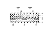
しかしながら、図6及び図7に示すフレキシブルプリント配線板では問題が生じる。図6に示すフレキシブルプリント配線板は、絶縁層110の片面に信号層として接着層125で接着した信号線120を配線し、もう一方の面を接着層135で接着したグラウンド層130とする。信号線120及びグラウンド層130の絶縁層110と反対の面は、それぞれ接着層125,135で可撓性を有する絶縁性のカバー層140,170が接着されている。図7に示すフレキシブルプリント配線板は、図6のフレキシブルプリント配線板と比してグラウンド層130がメッシュ構造となっている点がことなり、その他は実質的に同様である。図6及び図7に示すフレキシブルプリント配線板では、信号線120に高周波電流を流すと、信号線120から電磁放射が生じて、電磁障害(EMI)を起こすことにより、高速信号の伝達に悪影響を起こす問題が発生する。
本発明は、電磁放射を低減させることで、電磁障害を起こさないフレキシブルプリント配線板を提供することを目的とする。 An object of this invention is to provide the flexible printed wiring board which does not raise | generate an electromagnetic interference by reducing electromagnetic radiation.
本願発明の一態様によれば、可撓性を有する絶縁層と、絶縁層の一面に配線された信号線と、信号線が配線された絶縁層の他面に設けられたグラウンド層と、絶縁層と対向する信号線の面の反対の面側に設けられ、グラウンド層と導通するシールド層とを備えるフレキシブルプリント配線板であることを要旨とする。 According to one embodiment of the present invention, a flexible insulating layer, a signal line wired on one surface of the insulating layer, a ground layer provided on the other surface of the insulating layer wired with the signal line, and an insulating layer The gist of the invention is a flexible printed wiring board that is provided on the side opposite to the surface of the signal line facing the layer and includes a shield layer that is electrically connected to the ground layer.
本発明によれば、電磁放射を低減させることで、電磁障害を起こさないフレキシブルプリント配線板を提供することができる。 According to the present invention, it is possible to provide a flexible printed wiring board that does not cause electromagnetic interference by reducing electromagnetic radiation.
以下に図面を参照して、本発明の実施の形態を説明する。以下の図面の記載において、同一又は類似の部分には同一又は類似の符号で表している。但し、図面は模式的なものであり、厚みと平面寸法との関係、各層の厚みの比率等は現実のものとは異なる。したがって、具体的な厚みや寸法は以下の説明を照らし合わせて判断するべきものである。また、図面相互間においても互いの寸法の関係や比率が異なる部分が含まれていることは勿論である。 Embodiments of the present invention will be described below with reference to the drawings. In the following description of the drawings, the same or similar parts are denoted by the same or similar reference numerals. However, the drawings are schematic, and the relationship between the thickness and the planar dimensions, the ratio of the thickness of each layer, and the like are different from the actual ones. Therefore, specific thicknesses and dimensions should be determined in light of the following description. Moreover, it is a matter of course that portions having different dimensional relationships and ratios are included between the drawings.
(第1の実施の形態)
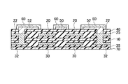
本発明の第1の実施の形態に係るフレキシブルプリント配線板は、図1に示すように、可撓性を有する絶縁層10と、絶縁層10の一面に配線された信号線20と、信号線20が配線された絶縁層10の他面に設けられたグラウンド層30と、絶縁層10と対向する信号線20の面の反対の面側に設けられ、グラウンド層30と導通するシールド層50とを備える。
(First embodiment)
As shown in FIG. 1, the flexible printed wiring board according to the first embodiment of the present invention includes a
絶縁層10としては、例えばポリイミド基板、ポリエチレンテレフタレート(PET)基板、ポリエチレンナフタレート(PEN)基板等の可撓性を有するフレキシブル基板を用いることができる。絶縁層10の厚さは、25μm、12.5μm、8μm、6μm等を採用することができる。
As the
信号線20は、圧延銅箔または電解銅箔等によりパターン加工して形成される。信号線20は、接着層25によって絶縁層10上に接着される。信号線20には、銅箔以外の金属箔を導体として使うことも可能である。信号線20のパターン幅は10〜500μmを採用することができ、好ましくは50〜300μm、更に好ましくは70〜150μmとする。信号線20の厚さは、35μm、33μm、18μm、12μm、9μm等を採用することができる。信号線20のピッチ幅は、10〜500μmを採用することができ、好ましくは、60〜300μm、更に好ましくは70〜150μmとする。信号線20が複数配線される場合、信号線20の信号層には、絶縁層10に設けられたスルーホールを介してグラウンド層30と電気的に導通する補助導線22が配線される。補助導線22は、信号線20間のノイズを防ぐ。
The
グラウンド層30は、接着層35によって絶縁層10上に接着される。グラウンド層30は、信号層の信号線20から電磁放射が発生することによって生じるEMIを防ぐために設けられている。グラウンド層30の厚さは、35μm、33μm、18μm、12μm、9μm等を採用することができる。
The
信号線20の接続端子部を除いた箇所、及びグラウンド層30上にはそれぞれ接着層25,35によって、接着後も優れた柔軟性を有する絶縁性のポリイミドフィルム等を基材にしたカバーレイやレジストの保護層40,70を配置する。保護層40で保護されていない信号線20の接続端子部等の露出している導体には、プリフラックス処理、ホットエアレベラ(HAL)、電解半田めっき、及び無電解半田めっき等で表面処理を行う。
A cover lay made of an insulating polyimide film or the like having excellent flexibility even after bonding is provided by
シールド層50は、保護層40に設けられたスルーホールを介して補助導線22と電気的に導通し、更にグラウンド層30とも電気的に導通している。シールド層50は、グラウンド層30と同様に、信号層の信号線20から電磁放射が発生することによって生じるEMIを防ぐために設けられている。シールド層50は、銀ペースト及び動ペースト等の導電性ペーストを印刷する、又は、導電性の導電性シールドテープを貼り付けて設けられる。シールド層50の厚さは、0.05〜100μmを採用することができ、好ましくは、0.1〜50μm、更に好ましくは0.2〜30μmとする。
The
導電カーボン層60は、導電性ペーストのイオンの移動によるマイグレーションを防ぐためにシールド層50上に設けられる。導電カーボン層60は、カーボンペースト等の印刷で設けられる。導電カーボン層60は、導電性であるので、シールド層50と導電カーボン層60でEMIを防ぐシールドの役割を果たす。導電カーボン層60の厚さは、3〜100μmを採用することができ、好ましくは、5〜50μm、更に好ましくは10〜30μmとする。
The
第1の実施の形態に係るフレキシブルプリント配線板によれば、信号線20に高周波電流を流した場合でも、信号線20を配置した面側にシールド層50を設けていることにより、信号線20から発する電磁放射を低減させて、EMI特性を向上させることができる。
According to the flexible printed wiring board according to the first embodiment, even when a high-frequency current is passed through the
(第2の実施の形態)
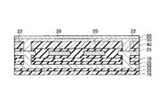
本発明の第2の実施の形態に係るフレキシブルプリント配線板は、図2に示すように、図1で示したフレキシブルプリント配線板と比して、グラウンド層30,32及びシールド層50,52がメッシュ構造になっている点が異なる。他は図1に示したフレキシブルプリント配線板と実質的に同様であるので、重複した記載を省略する。
(Second Embodiment)
As shown in FIG. 2, the flexible printed wiring board according to the second embodiment of the present invention has
グラウンド層30,32は、垂直及び所定の角度に交差することでメッシュ構造を形成する。グラウンド層32は、絶縁層10に設けられたスルーホールを介して信号層の補助導線22と電気的に導通している。グラウンド層30,32のパターン幅は10〜500μmを採用することができ、好ましくは50〜300μm、更に好ましくは70〜150μmとする。グラウンド層30,32のピッチ幅は、20〜2000μmを採用することができ、好ましくは、100〜950μm、更に好ましくは400〜900μmとする。グラウンド層30,32の厚さは、35μm、33μm、18μm、12μm、9μm等を採用することができる。
The
シールド層50,52は、垂直及び所定の角度に交差することでメッシュ構造を形成する。シールド層52は、保護層40に設けられたスルーホールを介して信号層の補助導線22と電気的に導通している。シールド層50,52の厚さは、0.05〜100μmを採用することができ、好ましくは、0.1〜50μm、更に好ましくは0.2〜30μmとする。
The
導電カーボン層60は、シールド層50,52を覆うように設けられているので、シールド層50,52と同様にメッシュ構造になっている。導電カーボン層60は、導電性であるのでシールド層50,52と共に、信号層の信号線20から電磁放射が発生することによって生じるEMIを防ぐシールドとして作用する。導電カーボン層60の厚さは、3〜100μmを採用することができ、好ましくは、5〜50μm、更に好ましくは10〜30μmとする。
Since the
第2の実施の形態に係るフレキシブルプリント配線板によれば、信号線20に高周波電流を流した場合でも、信号線20を配置した面側にシールド層50,52を設けていることにより、信号線20から発する電磁放射を低減させて、EMI特性を向上させることができる。
According to the flexible printed wiring board according to the second embodiment, even when a high-frequency current is passed through the
また、第2の実施の形態に係るフレキシブルプリント配線板によれば、グラウンド層30,32及びシールド層50,52がメッシュ構造であるので、フレキシブルプリント配線板の屈曲性を損なわない。 Moreover, according to the flexible printed wiring board which concerns on 2nd Embodiment, since the ground layers 30 and 32 and the shield layers 50 and 52 are mesh structures, the flexibility of a flexible printed wiring board is not impaired.
更に、第2の実施の形態に係るフレキシブルプリント配線板によれば、グラウンド層30,32及びシールド層50,52がメッシュ構造とすることにより回路のインピーダンスを所望の値とすることができる。 Furthermore, according to the flexible printed wiring board according to the second embodiment, the ground layers 30 and 32 and the shield layers 50 and 52 have a mesh structure, whereby the impedance of the circuit can be set to a desired value.
(第3の実施の形態)
本発明の第3の実施の形態に係るフレキシブルプリント配線板は、図3に示すように、図1で示したフレキシブルプリント配線板と比して、グラウンド層30,32及びシールド層50,52がメッシュ構造になっている点と、導電カーボン層60が絶縁性の絶縁カーボン層65になっている点が異なる。他は図1に示したフレキシブルプリント配線板と実質的に同様であるので、重複した記載を省略する。
(Third embodiment)
As shown in FIG. 3, the flexible printed wiring board according to the third embodiment of the present invention has ground layers 30 and 32 and shield layers 50 and 52 as compared with the flexible printed wiring board shown in FIG. The difference is that it has a mesh structure and the
絶縁カーボン層65は、導電性ペーストのイオンの移動によるマイグレーションを防ぐためにシールド層50,52上に設けられる。絶縁カーボン層65は、カーボンを含有するが絶縁性のカーボンペースト等を印刷することで設けられる。絶縁カーボン層65の厚さは、3〜100μmを採用することができ、好ましくは、5〜50μm、更に好ましくは10〜30μmとする。
The insulating
第3の実施の形態に係るフレキシブルプリント配線板によれば、信号線20に高周波電流を流した場合でも、信号線20を配置した面側にシールド層50,52を設けていることにより、信号線20から発する電磁放射を低減させて、EMI特性を向上させることができる。
According to the flexible printed wiring board according to the third embodiment, even when a high frequency current is passed through the
また、第3の実施の形態に係るフレキシブルプリント配線板によれば、グラウンド層30,32及びシールド層50,52がメッシュ構造であるので、フレキシブルプリント配線板の屈曲性を損なわない。 Moreover, according to the flexible printed wiring board concerning 3rd Embodiment, since the ground layers 30 and 32 and the shield layers 50 and 52 are mesh structures, the flexibility of a flexible printed wiring board is not impaired.
更に、第3の実施の形態に係るフレキシブルプリント配線板によれば、グラウンド層30,32及びシールド層50,52がメッシュ構造とすることにより回路のインピーダンスを所望の値とすることができる。 Furthermore, according to the flexible printed wiring board according to the third embodiment, the ground layers 30 and 32 and the shield layers 50 and 52 have a mesh structure, whereby the impedance of the circuit can be set to a desired value.
(実施例)
以下に、メッシュ構造のグラウンド層30,32のピッチ幅と差動回路の差動インピーダンスの関係を示すための実施例を記載する。
(Example)
In the following, an embodiment for showing the relationship between the pitch width of the ground layers 30 and 32 having a mesh structure and the differential impedance of the differential circuit will be described.
実施例としてのフレキシブルプリント配線板は、絶縁層10に厚さが25μmのポリイミド基板を用いる。信号線20、補助導線22、及びグラウンド層30,32は、絶縁層10の両面に接着剤厚20μmで接着した厚さ18μmの銅箔で形成する。保護層40,70には、接着剤厚35μmで接着した厚さ25μmのポリイミドフィルムをカバーレイとして用いる。
The flexible printed wiring board as an example uses a polyimide substrate having a thickness of 25 μm for the insulating
実施例における、信号線20とグラウンド層30,32のメッシュ構造の位置関係は、信号線20がグラウンド層30,32のメッシュ構造の交点で38°と52°に二分するように交わる位置関係とする。
In the embodiment, the positional relationship between the mesh structure of the
信号線20は、パターン幅を100μm、ピッチ幅を200μmとする。グラウンド層30,32は、パターン幅を150μmで固定する。そして、グラウンド層30,32のピッチ幅を、200μm、300μm、400μm、500μm、600μm、700μm、800μm、900μmと変化させる。
The
グラウンド層30,32のピッチ幅を変化させたときの、グラウンド層30,32のピッチ幅と差動インピーダンスの関係を図4及び図5に示す。図4のグラフに示す関係はシールド層50がメッシュ構造でない場合であり、図5のグラフに示す関係はシールド層50,52が上記のグラウンド層30,32のピッチ幅と同様に変化するメッシュ構造である場合である。
4 and 5 show the relationship between the pitch width of the ground layers 30 and 32 and the differential impedance when the pitch width of the ground layers 30 and 32 is changed. The relationship shown in the graph of FIG. 4 is when the
図4のグラフより、メッシュ構造であるグラウンド層30,32のピッチ幅を大きくする(メッシュの残銅が少なくなる)と、差動インピーダンスは上昇する。ピッチ幅(メッシュの残銅)を調整することにより、インピーダンスを所望の値に設計することが可能である。例えば、差動インピーダンスを100Ωに設計する場合は、グラウンド層30,32のピッチ幅を900μmにすればよい。 From the graph of FIG. 4, when the pitch width of the ground layers 30 and 32 having a mesh structure is increased (the remaining copper in the mesh is reduced), the differential impedance increases. By adjusting the pitch width (remaining copper of the mesh), it is possible to design the impedance to a desired value. For example, when the differential impedance is designed to be 100Ω , the pitch width of the ground layers 30 and 32 may be set to 900 μm.
次に、図5のグラフより、メッシュ構造であるグラウンド層30,32及びシールド層50,52のピッチ幅を大きくする(メッシュの残銅が少なくなる)と、差動インピーダンスは上昇する。ピッチ幅(メッシュの残銅)を調整することにより、インピーダンスを所望の値に設計することが可能である。例えば、差動インピーダンスを100Ωに設計する場合は、グラウンド層30,32及びシールド層50,52のピッチ幅を550μmにすればよい。 Next, from the graph of FIG. 5, when the pitch width of the ground layers 30 and 32 and the shield layers 50 and 52 having a mesh structure is increased (remaining copper in the mesh is reduced), the differential impedance increases. By adjusting the pitch width (remaining copper of the mesh), it is possible to design the impedance to a desired value. For example, when the differential impedance is designed to be 100Ω, the pitch width of the ground layers 30 and 32 and the shield layers 50 and 52 may be set to 550 μm.
(その他の実施の形態)
上記のように、本発明は実施の形態によって記載したが、この開示の一部をなす記述及び図面はこの発明を限定するものであると理解するべきではない。この開示から当業者には様々な代替実施の形態、実施例及び運用技術が明らかになるはずである。
(Other embodiments)
As described above, the present invention has been described according to the embodiment. However, it should not be understood that the description and drawings constituting a part of this disclosure limit the present invention. From this disclosure, various alternative embodiments, examples and operational techniques should be apparent to those skilled in the art.
例えば、第1の実施の形態で示したフレキシブルプリント配線板は、シールド層50上に導電性の導電カーボン層60を設けているが、絶縁性の絶縁カーボン層を設けてもよい。更に、絶縁カーボン層は、図2で示したように、シールド層50,52を覆ってメッシュ構造にしても構わない。
For example, in the flexible printed wiring board shown in the first embodiment, the
または、実施例において、グラウンド層30,32のピッチ幅とシールド層50,52のピッチ幅を同様に変化させることで、同じメッシュ構造のパターンとしたが、グラウンド層30,32のパターンとシールド層50,52のパターンは異なっても構わない。
Alternatively, in the embodiment, the same mesh structure pattern is obtained by changing the pitch width of the ground layers 30 and 32 and the pitch width of the shield layers 50 and 52 in the same manner, but the pattern of the ground layers 30 and 32 and the shield layer are the same. The
この様に、本発明はここでは記載していない様々な実施の形態等を包含するということを理解すべきである。したがって、本発明はこの開示から妥当な特許請求の範囲の発明特定事項によってのみ限定されるものである。 Thus, it should be understood that the present invention includes various embodiments and the like not described herein. Therefore, the present invention is limited only by the invention specifying matters in the scope of claims reasonable from this disclosure.
10…絶縁層
20…信号線
22…補助導線
25…接着層
30,32…グラウンド層
35…接着層
40,70…保護層
50,52…シールド層
60…導電カーボン層
65…絶縁カーボン層
110…絶縁層
120…信号線
125…接着層
125,135…接着層
130…グラウンド層
140,170…カバー層
DESCRIPTION OF
Claims (5)
前記絶縁層の一面に配線された信号線と、
前記信号線が配線された前記絶縁層の他面に設けられたグラウンド層と、
前記絶縁層と対向する前記信号線の面の反対の面側に設けられ、前記グラウンド層と導通するシールド層
とを備えることを特徴とするフレキシブルプリント配線板。 An insulating layer having flexibility;
A signal line wired on one surface of the insulating layer;
A ground layer provided on the other surface of the insulating layer to which the signal line is wired;
A flexible printed wiring board comprising: a shield layer provided on a surface opposite to the surface of the signal line facing the insulating layer and electrically connected to the ground layer.
Priority Applications (1)
| Application Number | Priority Date | Filing Date | Title |
|---|---|---|---|
| JP2006162349A JP2007335455A (en) | 2006-06-12 | 2006-06-12 | Flexible printed wiring board |
Applications Claiming Priority (1)
| Application Number | Priority Date | Filing Date | Title |
|---|---|---|---|
| JP2006162349A JP2007335455A (en) | 2006-06-12 | 2006-06-12 | Flexible printed wiring board |
Publications (1)
| Publication Number | Publication Date |
|---|---|
| JP2007335455A true JP2007335455A (en) | 2007-12-27 |
Family
ID=38934675
Family Applications (1)
| Application Number | Title | Priority Date | Filing Date |
|---|---|---|---|
| JP2006162349A Pending JP2007335455A (en) | 2006-06-12 | 2006-06-12 | Flexible printed wiring board |
Country Status (1)
| Country | Link |
|---|---|
| JP (1) | JP2007335455A (en) |
Cited By (7)
| Publication number | Priority date | Publication date | Assignee | Title |
|---|---|---|---|---|
| JP2010103537A (en) * | 2008-10-21 | 2010-05-06 | Ever Techno Co Ltd | Flexible printed circuit board for large-capacity signal transmission medium |
| KR100992323B1 (en) | 2008-06-27 | 2010-11-05 | 삼성전기주식회사 | Flexible circuit board and camera module using thereof |
| JP2010263031A (en) * | 2009-05-01 | 2010-11-18 | Nitto Denko Corp | Printed circuit board and magnetic head driving device including the same |
| WO2011016192A1 (en) * | 2009-08-07 | 2011-02-10 | 住友ベークライト株式会社 | Circuit board |
| JP2014509447A (en) * | 2011-01-05 | 2014-04-17 | トムソン ライセンシング | Controlled impedance flexible circuit |
| WO2018199133A1 (en) * | 2017-04-28 | 2018-11-01 | 日東電工株式会社 | Flexible wiring circuit board, manufacturing method thereof, and imaging device |
| CN110603905A (en) * | 2017-04-28 | 2019-12-20 | 日东电工株式会社 | Flexible printed circuit board, method for manufacturing flexible printed circuit board, and imaging device |
Citations (7)
| Publication number | Priority date | Publication date | Assignee | Title |
|---|---|---|---|---|
| JPH0415256U (en) * | 1990-05-28 | 1992-02-06 | ||
| JPH07106787A (en) * | 1993-09-29 | 1995-04-21 | Fuji Xerox Co Ltd | Shielding device of flexible printed wiring board |
| JPH07122882A (en) * | 1993-06-03 | 1995-05-12 | Sumitomo Electric Ind Ltd | Shielded flexible printed wiring board |
| JPH08125380A (en) * | 1994-10-19 | 1996-05-17 | Sumitomo Electric Ind Ltd | Shielded flexible wiring-board and manufacturing method thereof |
| JP2000114728A (en) * | 1998-09-30 | 2000-04-21 | Matsushita Electric Ind Co Ltd | Flexible printed board |
| JP2005251958A (en) * | 2004-03-04 | 2005-09-15 | Fujikura Ltd | Flexible printed wiring board and bracket cable |
| JP2006140346A (en) * | 2004-11-12 | 2006-06-01 | Hitachi Chem Co Ltd | Electromagnetic wave shielding member and its manufacturing method |
-
2006
- 2006-06-12 JP JP2006162349A patent/JP2007335455A/en active Pending
Patent Citations (7)
| Publication number | Priority date | Publication date | Assignee | Title |
|---|---|---|---|---|
| JPH0415256U (en) * | 1990-05-28 | 1992-02-06 | ||
| JPH07122882A (en) * | 1993-06-03 | 1995-05-12 | Sumitomo Electric Ind Ltd | Shielded flexible printed wiring board |
| JPH07106787A (en) * | 1993-09-29 | 1995-04-21 | Fuji Xerox Co Ltd | Shielding device of flexible printed wiring board |
| JPH08125380A (en) * | 1994-10-19 | 1996-05-17 | Sumitomo Electric Ind Ltd | Shielded flexible wiring-board and manufacturing method thereof |
| JP2000114728A (en) * | 1998-09-30 | 2000-04-21 | Matsushita Electric Ind Co Ltd | Flexible printed board |
| JP2005251958A (en) * | 2004-03-04 | 2005-09-15 | Fujikura Ltd | Flexible printed wiring board and bracket cable |
| JP2006140346A (en) * | 2004-11-12 | 2006-06-01 | Hitachi Chem Co Ltd | Electromagnetic wave shielding member and its manufacturing method |
Cited By (9)
| Publication number | Priority date | Publication date | Assignee | Title |
|---|---|---|---|---|
| KR100992323B1 (en) | 2008-06-27 | 2010-11-05 | 삼성전기주식회사 | Flexible circuit board and camera module using thereof |
| JP2010103537A (en) * | 2008-10-21 | 2010-05-06 | Ever Techno Co Ltd | Flexible printed circuit board for large-capacity signal transmission medium |
| JP2010263031A (en) * | 2009-05-01 | 2010-11-18 | Nitto Denko Corp | Printed circuit board and magnetic head driving device including the same |
| US8330054B2 (en) | 2009-05-01 | 2012-12-11 | Nitto Denko Corporation | Printed circuit board and magnetic head driving device including the same |
| WO2011016192A1 (en) * | 2009-08-07 | 2011-02-10 | 住友ベークライト株式会社 | Circuit board |
| JP2014509447A (en) * | 2011-01-05 | 2014-04-17 | トムソン ライセンシング | Controlled impedance flexible circuit |
| WO2018199133A1 (en) * | 2017-04-28 | 2018-11-01 | 日東電工株式会社 | Flexible wiring circuit board, manufacturing method thereof, and imaging device |
| CN110603905A (en) * | 2017-04-28 | 2019-12-20 | 日东电工株式会社 | Flexible printed circuit board, method for manufacturing flexible printed circuit board, and imaging device |
| CN110603905B (en) * | 2017-04-28 | 2023-07-18 | 日东电工株式会社 | Flexible wiring circuit board, method for manufacturing flexible wiring circuit board, and imaging device |
Similar Documents
| Publication | Publication Date | Title |
|---|---|---|
| JP6426067B2 (en) | Multilayer flexible printed wiring board and method of manufacturing the same | |
| CN104754855A (en) | Flexible circuit board and manufacturing method thereof | |
| JP2007335455A (en) | Flexible printed wiring board | |
| JP2016063188A (en) | Printed wiring board | |
| JP2008091635A (en) | Wiring circuit board | |
| JP4757079B2 (en) | Wiring circuit board and manufacturing method thereof | |
| US20110036619A1 (en) | Flex-rigid wiring board and method for manufacturing the same | |
| JP2009206188A (en) | Flexible printed wiring board | |
| JP4933318B2 (en) | Printed circuit board assembly and inverter using the printed circuit board assembly | |
| JP2006270026A (en) | Wiring structure, printed wiring board, integrated circuit, and electronic device | |
| KR20190099712A (en) | Printed Circuit Board and Electronic Device having the same | |
| JP2007073956A (en) | Printed circuit board assembly and electronic device utilizing it | |
| JP5092354B2 (en) | Double-sided printed wiring board, electronic device, and method for manufacturing double-sided printed wiring board | |
| JP2007234826A (en) | Flexible printed wiring board | |
| JP4838034B2 (en) | Printed wiring board and manufacturing method thereof | |
| KR200432681Y1 (en) | Shield layered FPCB | |
| JP2017120932A (en) | Printed Wiring Board | |
| JP2004228344A (en) | Multilayered fpc | |
| JP4838006B2 (en) | Flexible printed wiring board | |
| JP2008288516A (en) | Flexible substrate | |
| CN104284529A (en) | Rigid-flexible circuit board and manufacturing method thereof | |
| CN217849758U (en) | High-speed printed circuit board and electronic device | |
| CN212786019U (en) | Multilayer printed circuit board | |
| KR100779505B1 (en) | Printed circuit board comprising insert-hole for mounting electronic device | |
| CN112654129B (en) | Anti-electromagnetic interference circuit board and manufacturing method thereof |
Legal Events
| Date | Code | Title | Description |
|---|---|---|---|
| A621 | Written request for application examination |
Free format text: JAPANESE INTERMEDIATE CODE: A621 Effective date: 20081127 |
|
| A977 | Report on retrieval |
Free format text: JAPANESE INTERMEDIATE CODE: A971007 Effective date: 20101209 |
|
| A131 | Notification of reasons for refusal |
Effective date: 20101215 Free format text: JAPANESE INTERMEDIATE CODE: A131 |
|
| A521 | Written amendment |
Free format text: JAPANESE INTERMEDIATE CODE: A523 Effective date: 20110214 |
|
| A131 | Notification of reasons for refusal |
Free format text: JAPANESE INTERMEDIATE CODE: A131 Effective date: 20110308 |
|
| A02 | Decision of refusal |
Effective date: 20110726 Free format text: JAPANESE INTERMEDIATE CODE: A02 |