WO2021221055A1 - 半導体素子の製造方法 - Google Patents
半導体素子の製造方法 Download PDFInfo
- Publication number
- WO2021221055A1 WO2021221055A1 PCT/JP2021/016802 JP2021016802W WO2021221055A1 WO 2021221055 A1 WO2021221055 A1 WO 2021221055A1 JP 2021016802 W JP2021016802 W JP 2021016802W WO 2021221055 A1 WO2021221055 A1 WO 2021221055A1
- Authority
- WO
- WIPO (PCT)
- Prior art keywords
- semiconductor
- base substrate
- manufacturing
- substrate
- semiconductor element
- Prior art date
- Legal status (The legal status is an assumption and is not a legal conclusion. Google has not performed a legal analysis and makes no representation as to the accuracy of the status listed.)
- Ceased
Links
Images








Classifications
-
- H—ELECTRICITY
- H10—SEMICONDUCTOR DEVICES; ELECTRIC SOLID-STATE DEVICES NOT OTHERWISE PROVIDED FOR
- H10P—GENERIC PROCESSES OR APPARATUS FOR THE MANUFACTURE OR TREATMENT OF DEVICES COVERED BY CLASS H10
- H10P50/00—Etching of wafers, substrates or parts of devices
- H10P50/60—Wet etching
- H10P50/64—Wet etching of semiconductor materials
- H10P50/642—Chemical etching
- H10P50/646—Chemical etching of Group III-V materials
- H10P50/648—Anisotropic liquid etching
-
- H—ELECTRICITY
- H10—SEMICONDUCTOR DEVICES; ELECTRIC SOLID-STATE DEVICES NOT OTHERWISE PROVIDED FOR
- H10P—GENERIC PROCESSES OR APPARATUS FOR THE MANUFACTURE OR TREATMENT OF DEVICES COVERED BY CLASS H10
- H10P14/00—Formation of materials, e.g. in the shape of layers or pillars
- H10P14/20—Formation of materials, e.g. in the shape of layers or pillars of semiconductor materials
- H10P14/38—Formation of materials, e.g. in the shape of layers or pillars of semiconductor materials characterised by treatments done after the formation of the materials
-
- B—PERFORMING OPERATIONS; TRANSPORTING
- B23—MACHINE TOOLS; METAL-WORKING NOT OTHERWISE PROVIDED FOR
- B23K—SOLDERING OR UNSOLDERING; WELDING; CLADDING OR PLATING BY SOLDERING OR WELDING; CUTTING BY APPLYING HEAT LOCALLY, e.g. FLAME CUTTING; WORKING BY LASER BEAM
- B23K26/00—Working by laser beam, e.g. welding, cutting or boring
- B23K26/0006—Working by laser beam, e.g. welding, cutting or boring taking account of the properties of the material involved
-
- B—PERFORMING OPERATIONS; TRANSPORTING
- B23—MACHINE TOOLS; METAL-WORKING NOT OTHERWISE PROVIDED FOR
- B23K—SOLDERING OR UNSOLDERING; WELDING; CLADDING OR PLATING BY SOLDERING OR WELDING; CUTTING BY APPLYING HEAT LOCALLY, e.g. FLAME CUTTING; WORKING BY LASER BEAM
- B23K26/00—Working by laser beam, e.g. welding, cutting or boring
- B23K26/02—Positioning or observing the workpiece, e.g. with respect to the point of impact; Aligning, aiming or focusing the laser beam
- B23K26/06—Shaping the laser beam, e.g. by masks or multi-focusing
- B23K26/062—Shaping the laser beam, e.g. by masks or multi-focusing by direct control of the laser beam
- B23K26/0622—Shaping the laser beam, e.g. by masks or multi-focusing by direct control of the laser beam by shaping pulses
- B23K26/0624—Shaping the laser beam, e.g. by masks or multi-focusing by direct control of the laser beam by shaping pulses using ultrashort pulses, i.e. pulses of 1 ns or less
-
- B—PERFORMING OPERATIONS; TRANSPORTING
- B23—MACHINE TOOLS; METAL-WORKING NOT OTHERWISE PROVIDED FOR
- B23K—SOLDERING OR UNSOLDERING; WELDING; CLADDING OR PLATING BY SOLDERING OR WELDING; CUTTING BY APPLYING HEAT LOCALLY, e.g. FLAME CUTTING; WORKING BY LASER BEAM
- B23K26/00—Working by laser beam, e.g. welding, cutting or boring
- B23K26/50—Working by transmitting the laser beam through or within the workpiece
- B23K26/53—Working by transmitting the laser beam through or within the workpiece for modifying or reforming the material inside the workpiece, e.g. for producing break initiation cracks
-
- C—CHEMISTRY; METALLURGY
- C30—CRYSTAL GROWTH
- C30B—SINGLE-CRYSTAL GROWTH; UNIDIRECTIONAL SOLIDIFICATION OF EUTECTIC MATERIAL OR UNIDIRECTIONAL DEMIXING OF EUTECTOID MATERIAL; REFINING BY ZONE-MELTING OF MATERIAL; PRODUCTION OF A HOMOGENEOUS POLYCRYSTALLINE MATERIAL WITH DEFINED STRUCTURE; SINGLE CRYSTALS OR HOMOGENEOUS POLYCRYSTALLINE MATERIAL WITH DEFINED STRUCTURE; AFTER-TREATMENT OF SINGLE CRYSTALS OR A HOMOGENEOUS POLYCRYSTALLINE MATERIAL WITH DEFINED STRUCTURE; APPARATUS THEREFOR
- C30B25/00—Single-crystal growth by chemical reaction of reactive gases, e.g. chemical vapour-deposition growth
- C30B25/02—Epitaxial-layer growth
- C30B25/04—Pattern deposit, e.g. by using masks
-
- C—CHEMISTRY; METALLURGY
- C30—CRYSTAL GROWTH
- C30B—SINGLE-CRYSTAL GROWTH; UNIDIRECTIONAL SOLIDIFICATION OF EUTECTIC MATERIAL OR UNIDIRECTIONAL DEMIXING OF EUTECTOID MATERIAL; REFINING BY ZONE-MELTING OF MATERIAL; PRODUCTION OF A HOMOGENEOUS POLYCRYSTALLINE MATERIAL WITH DEFINED STRUCTURE; SINGLE CRYSTALS OR HOMOGENEOUS POLYCRYSTALLINE MATERIAL WITH DEFINED STRUCTURE; AFTER-TREATMENT OF SINGLE CRYSTALS OR A HOMOGENEOUS POLYCRYSTALLINE MATERIAL WITH DEFINED STRUCTURE; APPARATUS THEREFOR
- C30B25/00—Single-crystal growth by chemical reaction of reactive gases, e.g. chemical vapour-deposition growth
- C30B25/02—Epitaxial-layer growth
- C30B25/18—Epitaxial-layer growth characterised by the substrate
-
- C—CHEMISTRY; METALLURGY
- C30—CRYSTAL GROWTH
- C30B—SINGLE-CRYSTAL GROWTH; UNIDIRECTIONAL SOLIDIFICATION OF EUTECTIC MATERIAL OR UNIDIRECTIONAL DEMIXING OF EUTECTOID MATERIAL; REFINING BY ZONE-MELTING OF MATERIAL; PRODUCTION OF A HOMOGENEOUS POLYCRYSTALLINE MATERIAL WITH DEFINED STRUCTURE; SINGLE CRYSTALS OR HOMOGENEOUS POLYCRYSTALLINE MATERIAL WITH DEFINED STRUCTURE; AFTER-TREATMENT OF SINGLE CRYSTALS OR A HOMOGENEOUS POLYCRYSTALLINE MATERIAL WITH DEFINED STRUCTURE; APPARATUS THEREFOR
- C30B25/00—Single-crystal growth by chemical reaction of reactive gases, e.g. chemical vapour-deposition growth
- C30B25/02—Epitaxial-layer growth
- C30B25/18—Epitaxial-layer growth characterised by the substrate
- C30B25/20—Epitaxial-layer growth characterised by the substrate the substrate being of the same materials as the epitaxial layer
-
- C—CHEMISTRY; METALLURGY
- C30—CRYSTAL GROWTH
- C30B—SINGLE-CRYSTAL GROWTH; UNIDIRECTIONAL SOLIDIFICATION OF EUTECTIC MATERIAL OR UNIDIRECTIONAL DEMIXING OF EUTECTOID MATERIAL; REFINING BY ZONE-MELTING OF MATERIAL; PRODUCTION OF A HOMOGENEOUS POLYCRYSTALLINE MATERIAL WITH DEFINED STRUCTURE; SINGLE CRYSTALS OR HOMOGENEOUS POLYCRYSTALLINE MATERIAL WITH DEFINED STRUCTURE; AFTER-TREATMENT OF SINGLE CRYSTALS OR A HOMOGENEOUS POLYCRYSTALLINE MATERIAL WITH DEFINED STRUCTURE; APPARATUS THEREFOR
- C30B29/00—Single crystals or homogeneous polycrystalline material with defined structure characterised by the material or by their shape
- C30B29/10—Inorganic compounds or compositions
- C30B29/40—AIIIBV compounds wherein A is B, Al, Ga, In or Tl and B is N, P, As, Sb or Bi
- C30B29/403—AIII-nitrides
- C30B29/406—Gallium nitride
-
- C—CHEMISTRY; METALLURGY
- C30—CRYSTAL GROWTH
- C30B—SINGLE-CRYSTAL GROWTH; UNIDIRECTIONAL SOLIDIFICATION OF EUTECTIC MATERIAL OR UNIDIRECTIONAL DEMIXING OF EUTECTOID MATERIAL; REFINING BY ZONE-MELTING OF MATERIAL; PRODUCTION OF A HOMOGENEOUS POLYCRYSTALLINE MATERIAL WITH DEFINED STRUCTURE; SINGLE CRYSTALS OR HOMOGENEOUS POLYCRYSTALLINE MATERIAL WITH DEFINED STRUCTURE; AFTER-TREATMENT OF SINGLE CRYSTALS OR A HOMOGENEOUS POLYCRYSTALLINE MATERIAL WITH DEFINED STRUCTURE; APPARATUS THEREFOR
- C30B33/00—After-treatment of single crystals or homogeneous polycrystalline material with defined structure
- C30B33/06—Joining of crystals
-
- H—ELECTRICITY
- H10—SEMICONDUCTOR DEVICES; ELECTRIC SOLID-STATE DEVICES NOT OTHERWISE PROVIDED FOR
- H10D—INORGANIC ELECTRIC SEMICONDUCTOR DEVICES
- H10D84/00—Integrated devices formed in or on semiconductor substrates that comprise only semiconducting layers, e.g. on Si wafers or on GaAs-on-Si wafers
- H10D84/01—Manufacture or treatment
-
- H—ELECTRICITY
- H10—SEMICONDUCTOR DEVICES; ELECTRIC SOLID-STATE DEVICES NOT OTHERWISE PROVIDED FOR
- H10H—INORGANIC LIGHT-EMITTING SEMICONDUCTOR DEVICES HAVING POTENTIAL BARRIERS
- H10H20/00—Individual inorganic light-emitting semiconductor devices having potential barriers, e.g. light-emitting diodes [LED]
- H10H20/01—Manufacture or treatment
- H10H20/011—Manufacture or treatment of bodies, e.g. forming semiconductor layers
- H10H20/013—Manufacture or treatment of bodies, e.g. forming semiconductor layers having light-emitting regions comprising only Group III-V materials
- H10H20/0137—Manufacture or treatment of bodies, e.g. forming semiconductor layers having light-emitting regions comprising only Group III-V materials the light-emitting regions comprising nitride materials
-
- H—ELECTRICITY
- H10—SEMICONDUCTOR DEVICES; ELECTRIC SOLID-STATE DEVICES NOT OTHERWISE PROVIDED FOR
- H10P—GENERIC PROCESSES OR APPARATUS FOR THE MANUFACTURE OR TREATMENT OF DEVICES COVERED BY CLASS H10
- H10P14/00—Formation of materials, e.g. in the shape of layers or pillars
- H10P14/20—Formation of materials, e.g. in the shape of layers or pillars of semiconductor materials
- H10P14/27—Formation of materials, e.g. in the shape of layers or pillars of semiconductor materials using selective deposition, e.g. simultaneous growth of monocrystalline and non-monocrystalline semiconductor materials
- H10P14/271—Formation of materials, e.g. in the shape of layers or pillars of semiconductor materials using selective deposition, e.g. simultaneous growth of monocrystalline and non-monocrystalline semiconductor materials characterised by the preparation of substrate for selective deposition
- H10P14/272—Formation of materials, e.g. in the shape of layers or pillars of semiconductor materials using selective deposition, e.g. simultaneous growth of monocrystalline and non-monocrystalline semiconductor materials characterised by the preparation of substrate for selective deposition using mask materials other than SiO2 or SiN
-
- H—ELECTRICITY
- H10—SEMICONDUCTOR DEVICES; ELECTRIC SOLID-STATE DEVICES NOT OTHERWISE PROVIDED FOR
- H10P—GENERIC PROCESSES OR APPARATUS FOR THE MANUFACTURE OR TREATMENT OF DEVICES COVERED BY CLASS H10
- H10P14/00—Formation of materials, e.g. in the shape of layers or pillars
- H10P14/20—Formation of materials, e.g. in the shape of layers or pillars of semiconductor materials
- H10P14/27—Formation of materials, e.g. in the shape of layers or pillars of semiconductor materials using selective deposition, e.g. simultaneous growth of monocrystalline and non-monocrystalline semiconductor materials
- H10P14/276—Lateral overgrowth
-
- H—ELECTRICITY
- H10—SEMICONDUCTOR DEVICES; ELECTRIC SOLID-STATE DEVICES NOT OTHERWISE PROVIDED FOR
- H10P—GENERIC PROCESSES OR APPARATUS FOR THE MANUFACTURE OR TREATMENT OF DEVICES COVERED BY CLASS H10
- H10P14/00—Formation of materials, e.g. in the shape of layers or pillars
- H10P14/20—Formation of materials, e.g. in the shape of layers or pillars of semiconductor materials
- H10P14/29—Formation of materials, e.g. in the shape of layers or pillars of semiconductor materials characterised by the substrates
- H10P14/2901—Materials
- H10P14/2907—Materials being Group IIIA-VA materials
- H10P14/2908—Nitrides
-
- H—ELECTRICITY
- H10—SEMICONDUCTOR DEVICES; ELECTRIC SOLID-STATE DEVICES NOT OTHERWISE PROVIDED FOR
- H10P—GENERIC PROCESSES OR APPARATUS FOR THE MANUFACTURE OR TREATMENT OF DEVICES COVERED BY CLASS H10
- H10P14/00—Formation of materials, e.g. in the shape of layers or pillars
- H10P14/20—Formation of materials, e.g. in the shape of layers or pillars of semiconductor materials
- H10P14/34—Deposited materials, e.g. layers
- H10P14/3402—Deposited materials, e.g. layers characterised by the chemical composition
- H10P14/3414—Deposited materials, e.g. layers characterised by the chemical composition being group IIIA-VIA materials
- H10P14/3416—Nitrides
-
- H—ELECTRICITY
- H10—SEMICONDUCTOR DEVICES; ELECTRIC SOLID-STATE DEVICES NOT OTHERWISE PROVIDED FOR
- H10P—GENERIC PROCESSES OR APPARATUS FOR THE MANUFACTURE OR TREATMENT OF DEVICES COVERED BY CLASS H10
- H10P95/00—Generic processes or apparatus for manufacture or treatments not covered by the other groups of this subclass
- H10P95/11—Separation of active layers from substrates
- H10P95/112—Separation of active layers from substrates leaving a reusable substrate, e.g. epitaxial lift off
-
- B—PERFORMING OPERATIONS; TRANSPORTING
- B23—MACHINE TOOLS; METAL-WORKING NOT OTHERWISE PROVIDED FOR
- B23K—SOLDERING OR UNSOLDERING; WELDING; CLADDING OR PLATING BY SOLDERING OR WELDING; CUTTING BY APPLYING HEAT LOCALLY, e.g. FLAME CUTTING; WORKING BY LASER BEAM
- B23K2101/00—Articles made by soldering, welding or cutting
- B23K2101/36—Electric or electronic devices
- B23K2101/40—Semiconductor devices
-
- B—PERFORMING OPERATIONS; TRANSPORTING
- B23—MACHINE TOOLS; METAL-WORKING NOT OTHERWISE PROVIDED FOR
- B23K—SOLDERING OR UNSOLDERING; WELDING; CLADDING OR PLATING BY SOLDERING OR WELDING; CUTTING BY APPLYING HEAT LOCALLY, e.g. FLAME CUTTING; WORKING BY LASER BEAM
- B23K2103/00—Materials to be soldered, welded or cut
- B23K2103/50—Inorganic materials other than metals or composite materials
- B23K2103/56—Inorganic materials other than metals or composite materials being semiconducting
-
- H—ELECTRICITY
- H01—ELECTRIC ELEMENTS
- H01S—DEVICES USING THE PROCESS OF LIGHT AMPLIFICATION BY STIMULATED EMISSION OF RADIATION [LASER] TO AMPLIFY OR GENERATE LIGHT; DEVICES USING STIMULATED EMISSION OF ELECTROMAGNETIC RADIATION IN WAVE RANGES OTHER THAN OPTICAL
- H01S2304/00—Special growth methods for semiconductor lasers
- H01S2304/12—Pendeo epitaxial lateral overgrowth [ELOG], e.g. for growing GaN based blue laser diodes
-
- H—ELECTRICITY
- H01—ELECTRIC ELEMENTS
- H01S—DEVICES USING THE PROCESS OF LIGHT AMPLIFICATION BY STIMULATED EMISSION OF RADIATION [LASER] TO AMPLIFY OR GENERATE LIGHT; DEVICES USING STIMULATED EMISSION OF ELECTROMAGNETIC RADIATION IN WAVE RANGES OTHER THAN OPTICAL
- H01S5/00—Semiconductor lasers
- H01S5/02—Structural details or components not essential to laser action
- H01S5/0206—Substrates, e.g. growth, shape, material, removal or bonding
- H01S5/0217—Removal of the substrate
-
- H—ELECTRICITY
- H01—ELECTRIC ELEMENTS
- H01S—DEVICES USING THE PROCESS OF LIGHT AMPLIFICATION BY STIMULATED EMISSION OF RADIATION [LASER] TO AMPLIFY OR GENERATE LIGHT; DEVICES USING STIMULATED EMISSION OF ELECTROMAGNETIC RADIATION IN WAVE RANGES OTHER THAN OPTICAL
- H01S5/00—Semiconductor lasers
- H01S5/20—Structure or shape of the semiconductor body to guide the optical wave ; Confining structures perpendicular to the optical axis, e.g. index or gain guiding, stripe geometry, broad area lasers, gain tailoring, transverse or lateral reflectors, special cladding structures, MQW barrier reflection layers
- H01S5/22—Structure or shape of the semiconductor body to guide the optical wave ; Confining structures perpendicular to the optical axis, e.g. index or gain guiding, stripe geometry, broad area lasers, gain tailoring, transverse or lateral reflectors, special cladding structures, MQW barrier reflection layers having a ridge or stripe structure
-
- H—ELECTRICITY
- H01—ELECTRIC ELEMENTS
- H01S—DEVICES USING THE PROCESS OF LIGHT AMPLIFICATION BY STIMULATED EMISSION OF RADIATION [LASER] TO AMPLIFY OR GENERATE LIGHT; DEVICES USING STIMULATED EMISSION OF ELECTROMAGNETIC RADIATION IN WAVE RANGES OTHER THAN OPTICAL
- H01S5/00—Semiconductor lasers
- H01S5/30—Structure or shape of the active region; Materials used for the active region
- H01S5/32—Structure or shape of the active region; Materials used for the active region comprising PN junctions, e.g. hetero- or double- heterostructures
- H01S5/323—Structure or shape of the active region; Materials used for the active region comprising PN junctions, e.g. hetero- or double- heterostructures in AIIIBV compounds, e.g. AlGaAs-laser, InP-based laser
- H01S5/32308—Structure or shape of the active region; Materials used for the active region comprising PN junctions, e.g. hetero- or double- heterostructures in AIIIBV compounds, e.g. AlGaAs-laser, InP-based laser emitting light at a wavelength less than 900 nm
- H01S5/32341—Structure or shape of the active region; Materials used for the active region comprising PN junctions, e.g. hetero- or double- heterostructures in AIIIBV compounds, e.g. AlGaAs-laser, InP-based laser emitting light at a wavelength less than 900 nm blue laser based on GaN or GaP
-
- H—ELECTRICITY
- H01—ELECTRIC ELEMENTS
- H01S—DEVICES USING THE PROCESS OF LIGHT AMPLIFICATION BY STIMULATED EMISSION OF RADIATION [LASER] TO AMPLIFY OR GENERATE LIGHT; DEVICES USING STIMULATED EMISSION OF ELECTROMAGNETIC RADIATION IN WAVE RANGES OTHER THAN OPTICAL
- H01S5/00—Semiconductor lasers
- H01S5/40—Arrangement of two or more semiconductor lasers, not provided for in groups H01S5/02 - H01S5/30
- H01S5/4025—Array arrangements, e.g. constituted by discrete laser diodes or laser bar
-
- H—ELECTRICITY
- H10—SEMICONDUCTOR DEVICES; ELECTRIC SOLID-STATE DEVICES NOT OTHERWISE PROVIDED FOR
- H10H—INORGANIC LIGHT-EMITTING SEMICONDUCTOR DEVICES HAVING POTENTIAL BARRIERS
- H10H20/00—Individual inorganic light-emitting semiconductor devices having potential barriers, e.g. light-emitting diodes [LED]
- H10H20/01—Manufacture or treatment
-
- H—ELECTRICITY
- H10—SEMICONDUCTOR DEVICES; ELECTRIC SOLID-STATE DEVICES NOT OTHERWISE PROVIDED FOR
- H10H—INORGANIC LIGHT-EMITTING SEMICONDUCTOR DEVICES HAVING POTENTIAL BARRIERS
- H10H20/00—Individual inorganic light-emitting semiconductor devices having potential barriers, e.g. light-emitting diodes [LED]
- H10H20/01—Manufacture or treatment
- H10H20/011—Manufacture or treatment of bodies, e.g. forming semiconductor layers
- H10H20/013—Manufacture or treatment of bodies, e.g. forming semiconductor layers having light-emitting regions comprising only Group III-V materials
- H10H20/0133—Manufacture or treatment of bodies, e.g. forming semiconductor layers having light-emitting regions comprising only Group III-V materials with a substrate not being Group III-V materials
- H10H20/01335—Manufacture or treatment of bodies, e.g. forming semiconductor layers having light-emitting regions comprising only Group III-V materials with a substrate not being Group III-V materials the light-emitting regions comprising nitride materials
-
- H—ELECTRICITY
- H10—SEMICONDUCTOR DEVICES; ELECTRIC SOLID-STATE DEVICES NOT OTHERWISE PROVIDED FOR
- H10H—INORGANIC LIGHT-EMITTING SEMICONDUCTOR DEVICES HAVING POTENTIAL BARRIERS
- H10H20/00—Individual inorganic light-emitting semiconductor devices having potential barriers, e.g. light-emitting diodes [LED]
- H10H20/01—Manufacture or treatment
- H10H20/011—Manufacture or treatment of bodies, e.g. forming semiconductor layers
- H10H20/018—Bonding of wafers
-
- H—ELECTRICITY
- H10—SEMICONDUCTOR DEVICES; ELECTRIC SOLID-STATE DEVICES NOT OTHERWISE PROVIDED FOR
- H10P—GENERIC PROCESSES OR APPARATUS FOR THE MANUFACTURE OR TREATMENT OF DEVICES COVERED BY CLASS H10
- H10P34/00—Irradiation with electromagnetic or particle radiation of wafers, substrates or parts of devices
- H10P34/40—Irradiation with electromagnetic or particle radiation of wafers, substrates or parts of devices with high-energy radiation
- H10P34/42—Irradiation with electromagnetic or particle radiation of wafers, substrates or parts of devices with high-energy radiation with electromagnetic radiation, e.g. laser annealing
-
- H—ELECTRICITY
- H10—SEMICONDUCTOR DEVICES; ELECTRIC SOLID-STATE DEVICES NOT OTHERWISE PROVIDED FOR
- H10P—GENERIC PROCESSES OR APPARATUS FOR THE MANUFACTURE OR TREATMENT OF DEVICES COVERED BY CLASS H10
- H10P50/00—Etching of wafers, substrates or parts of devices
- H10P50/60—Wet etching
- H10P50/61—Electrolytic etching
- H10P50/617—Electrolytic etching of Group III-V materials
Definitions
- the present invention relates to a method for manufacturing a semiconductor device.
- Patent Document 1 In the method of manufacturing a semiconductor element, various techniques for separating a semiconductor layer formed on a substrate from the substrate have been proposed (see, for example, Patent Document 1 below).
- semiconductor layers adjacent to each other in the direction along the first surface are separated from each other at least partially in the direction along the first surface on the first surface of the base substrate.
- a separation step of separating the plurality of semiconductor layers from the base substrate is included.
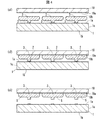
- step a shows a forming step
- step b shows a weakening step
- step c shows a separation step
- step a1 shows a mask forming step
- step “a2” shows a semiconductor layer forming step
- step a3 shows a mask removing step.
- step c1 indicates a preparation step
- step c2 indicates a joining step
- step c3 indicates a peeling step.
- the method for manufacturing a semiconductor device of the present embodiment includes a forming step a, a fragility step b, and a separation step c.
- the forming step a is one of epitaxial vapor deposition, for example, by the selective lateral growth (ELO) method, each of which is connected to the base substrate 1 by the connecting portion 2 on the base substrate 1.
- ELO selective lateral growth
- This is a step of forming a plurality of semiconductor layers 3.
- the weakening step b is a step of irradiating the connecting portion 2 with the laser beam 5 to weaken the connecting portion 2.
- the separation step c is a step of separating the plurality of semiconductor layers 3 from the base substrate 1.
- Each semiconductor layer 3 has, for example, a cleavage plane, and further, electrodes, wiring conductors, and the like are arranged to form one or a plurality of semiconductor elements S.
- the semiconductor element S include, but are not limited to, a light emitting diode (Light Emitting Diode; LED), a semiconductor laser (Laser Diode; LD), a photodiode (Photodiode; PD), and the like.
- the base substrate 1 has a flat one main surface (hereinafter, also referred to as a first surface) 1a including a starting point of growth of a semiconductor crystal, and a flat other main surface (hereinafter, also referred to as a second surface) opposite to the first surface 1a. It has 1b and a side surface (hereinafter, also referred to as a third surface) 1c connecting the first surface 1a and the second surface 1b. At least the first surface 1a of the base substrate 1 is made of a nitride semiconductor.
- the base substrate 1 may be, for example, a substrate made of a nitride semiconductor such as gallium nitride (GaN), aluminum gallium nitride (AlGaN), or indium gallium nitride (InGaN).
- a nitride semiconductor such as gallium nitride (GaN), aluminum gallium nitride (AlGaN), or indium gallium nitride (InGaN).
- the base substrate 1 used in the present embodiment is a GaN substrate cut out from a GaN single crystal ingot.
- the base substrate 1 is cut out from the single crystal ingot so that the first surface 1a including the starting point of the growth of the semiconductor crystal is in a predetermined surface direction.
- the base substrate 1 may be an n-type substrate in which impurities such as Si are doped in GaN, or may be a p-type substrate in which impurities such as Mg are doped in GaN.
- the impurity density in the base substrate 1 is, for example, about 1 ⁇ 10 19 cm -3 or less.
- the forming step a is a step of forming a plurality of semiconductor layers 3 on the first surface 1a of the base substrate 1 by the ELO method.
- a plurality of semiconductor layers 3 are formed so that the semiconductor layers 3 adjacent to each other in the direction along the first surface 1a are separated from each other at least partially in the direction along the first surface 1a.
- the forming step a includes a mask forming step a1, a semiconductor layer forming step a2, and a mask removing step a3, which are shown below.
- the mask forming step a1 is a step of forming a deposition suppressing mask (hereinafter, also simply referred to as a mask) 6 that suppresses the crystals of semiconductor crystals on the base substrate 1.
- a deposition suppressing mask hereinafter, also simply referred to as a mask
- silicon oxide for example, SiO 2 or the like
- PCVD plasma chemical vapor deposition
- the silicon oxide layer is then patterned using, for example, a photolithography method and wet etching with Buffered Hydrogen Fluoride (BHF). In this way, the mask 6 is formed on the first surface 1a in a predetermined pattern.
- the mask 6 may have, for example, a striped shape in which a plurality of strip-shaped portions 61 are arranged in parallel at predetermined intervals.
- the width of the opening 62, which is also called a mask window, between two adjacent strips 61 is, for example, about 2 ⁇ m to 20 ⁇ m.
- the width of the strip 61 is, for example, about 50 ⁇ m to 200 ⁇ m.
- the edge region near the third surface 1c on the first surface 1a of the base substrate 1 may also be covered with the mask 6. This makes it possible to cleanly and surely separate the semiconductor layer 3 that grows in the edge region of the first surface 1a from the base substrate 1. Further, it is possible to suppress the abnormal growth of the semiconductor crystal in the edge region of the first surface 1a.
- A2 Semiconductor layer forming step
- a GaN crystal is vapor-deposited from a region of the first surface 1a of the base substrate 1 that is not covered by the mask 6 and is exposed to the opening 62. Let me.
- VPE vapor phase deposition
- MOCVD Metalorganic Chemical Vapor Deposition
- the semiconductor layer 3 is formed into a light emitting diode (LED) or a semiconductor laser (Laser Diode;). It can be formed as a multilayer film that functions as an LD) or the like.
- the semiconductor crystal When the grown semiconductor crystal exceeds the opening 62 of the mask 6, the semiconductor crystal also grows laterally along the upper surface of the mask 6.
- the growth of the semiconductor crystal may be terminated before the semiconductor crystal grown from the first surface 1a overlaps with the adjacent semiconductor crystal.
- a plurality of semiconductor layers 3 are obtained, each of which is connected to the first surface 1a by the connecting portion 2.
- the connecting portion 2 is made of, for example, a GaN crystal.
- the connecting portion 2 has, for example, a width of about 2 ⁇ m to 20 ⁇ m and a height of about 100 nm to 500 nm.
- Each semiconductor layer 3 has, for example, a width of about 50 ⁇ m to 200 ⁇ m and a height of about 10 ⁇ m to 50 ⁇ m.
- the growth of the semiconductor crystal may continue until the semiconductor crystal that grows laterally along the upper surface of the mask 6 overlaps with the adjacent semiconductor crystal. In this case, a semiconductor layer connected to the first surface 1a by a plurality of connecting portions 2 is obtained.
- the mask removing step a3 is a step of removing the mask 6 after the completion of the semiconductor layer forming step a2.
- the base substrate 1 on which the semiconductor layer 3 is formed is taken out from the vapor phase growth apparatus (epitaxial apparatus), and the mask 6 is removed using an etchant that does not substantially invade the semiconductor layer 3.
- the mask 6 when the mask 6 is made of a silicon oxide film, the mask 6 is removed by performing wet etching using BHF. In this way, for example, as shown in FIG. 1, a plurality of semiconductor layers 3 are obtained, each of which is connected to the first surface 1a by a connecting portion 2.
- Each of the plurality of semiconductor layers 3 may extend in a predetermined direction in a plan view. Further, the plurality of semiconductor layers 3 may form a pattern as shown in FIG. 3, for example, in a plan view. The plurality of semiconductor layers 3 may form a striped pattern extending in a predetermined direction, for example, as shown in FIG. 3A. As shown in FIG. 3B, for example, the plurality of semiconductor layers 3 may be arranged in a staggered pattern to form a so-called repeat pattern. As shown in FIG. 3C, for example, the plurality of semiconductor layers 3 may form a grid-like pattern in which each semiconductor layer 3 is connected to adjacent semiconductor layers 3 at both ends thereof.
- the weakening step b is a step of irradiating the connecting portion 2 with the laser beam 5 to weaken the connecting portion 2.
- the connection portion 2 can be thermally denatured and the crystal structure of the connection portion 2 can be changed by irradiating the laser beam 5.
- the connection portion 2 may be completely or partially cut by the irradiation of the laser beam 5.
- the wavelength of the laser beam 5 may be, for example, 370 nm or less.
- a light source that outputs the laser beam 5 for example, an AlGAN-based semiconductor laser, a KrF excimer laser, an ArF excimer laser, a YAG laser (third harmonic), or the like can be used.
- the focal length and spot size of the laser beam 5 can be appropriately selected according to the dimensions of the base substrate 1, the connecting portion 2, the semiconductor layer 3, and the like.
- the laser beam 5 may be irradiated from the first surface 1a side of the base substrate 1 or may be irradiated from the second surface 1b side of the base substrate 1.
- the laser beam 5 may be irradiated from the third surface 1c side of the base substrate 1.
- the separation step c is a step of separating a plurality of semiconductor layers 3 from the base substrate 1.
- a force is applied to the weakened connecting portion 2 by, for example, bringing the blade into contact with the semiconductor layer 3 or irradiating the connecting portion 2 with ultrasonic waves.
- the connection portion 2 can be broken and the semiconductor layer 3 can be separated from the base substrate 1.
- the separation step c can be omitted.
- the plurality of semiconductor layers 3 formed on the first surface 1a of the base substrate 1 include semiconductor layers 3 adjacent to each other in the direction along the first surface 1a. It is at least partially separated in the direction along the first surface 1a. Therefore, the decomposition product gas or the evaporation gas generated by irradiating the connection portion 2 with the laser beam 5 and filling the space between the semiconductor layer 3 and the base substrate 1 can be discharged to the outside.
- the gas can be released to the outside through, for example, a gap (hereinafter, also referred to as a release path) G between adjacent semiconductor layers 3 as shown by an arrow in FIG.
- the base substrate 1 can be reused without polishing for removing the damaged portion or by performing only a small amount of polishing. As a result, it is possible to improve the production efficiency of the semiconductor element S, and it is possible to provide the semiconductor element S that can increase the number of times that the base substrate 1 can be reused.
- the method for manufacturing a semiconductor element of the present embodiment it is not necessary to irradiate the entire base substrate 1 with the laser beam 5, and it is sufficient to irradiate only the connecting portion 2 connecting each semiconductor layer 3 and the first surface 1a. .. Therefore, it is possible to suppress excessive heating of the semiconductor layer 3 and the base substrate 1, and it is possible to reduce thermal damage to the semiconductor layer 3 and the base substrate 1. As a result, it becomes possible to manufacture a high-quality semiconductor element S. Further, the base substrate 1 can be reused without polishing for removing the damaged portion or by performing only a small amount of polishing. This makes it possible to improve the production efficiency of the semiconductor element S and reduce the manufacturing cost of the semiconductor element S.
- the base substrate 1, the connecting portion 2, and the semiconductor layer 3 are made of GaN crystals, their refractive indexes are substantially the same. Thereby, the refraction and reflection of the laser beam 5 at the interface between the base substrate 1 and the connecting portion 2 and the interface between the connecting portion 2 and the semiconductor layer 3 can be reduced. As a result, the laser beam 5 can be irradiated to the connection portion 2 with high accuracy and high efficiency. As a result, it becomes possible to manufacture a high-quality semiconductor element S. Further, the production efficiency of the semiconductor element S can be improved.
- the fragility step b is performed. Before this is performed, a through hole may be formed in the semiconductor layer so as to penetrate in the thickness direction thereof. As a result, the decomposition product gas or the evaporation gas that fills the space between the semiconductor layer and the base substrate 1 can be discharged to the outside through the through holes. As a result, even when the semiconductor layer connected to the first surface 1a is formed by the plurality of connecting portions 2, it becomes possible to manufacture the high-quality semiconductor element S and the production efficiency of the semiconductor element S. Can be improved.
- the laser beam 5 may be irradiated from the second surface 1b side of the base substrate 1 and incident on the base substrate 1 from the second surface 1b. Since the base substrate 1 is not a dissimilar substrate formed by forming a GaN layer on the surface of a sapphire substrate, a SiC substrate, or the like, but a substrate made of substantially the same material, the refractive index of the base substrate 1 is substantially constant. Therefore, by incident the laser light 5 from the second surface 1b of the base substrate 1, the laser light 5 can be focused on the connection portion 2 with high accuracy.
- connection portion 2 may be irradiated with picosecond pulse laser light or femtosecond pulse laser light.
- picosecond pulse laser light or femtosecond pulse laser light.
- an ablation phenomenon due to multiphoton absorption can be induced at the connection portion 2 which is the condensing point of the laser beam 5. Therefore, the connection portion 2 can be fragile with high accuracy while suppressing the occurrence of thermal damage in the semiconductor layer 3 and the base substrate 1.
- connection portion 2 may be irradiated with a sub-nanosecond pulse laser beam or a nanosecond pulse laser beam.
- the material removal rate is higher than in the case where the pulse width of the laser beam 5 is picoseconds or femtoseconds, so that the processing efficiency in the weakening step b can be improved.
- the decomposition product gas and the evaporation gas can be effectively emitted to the outside even when the pulse width of the laser beam 5 is sub-nanoseconds or nanoseconds.
- the optimization of the emission path G may be to form each semiconductor layer 3 so as to have a cross-sectional shape in which the corners of the lower surface are rounded, as shown in FIG. 1, for example.
- a plurality of semiconductor layers 3 arranged in a staggered pattern are formed, and the distance between the adjacent semiconductor layers 3 is set in two different directions. It may be to adjust.
- a scanning path that improves the production efficiency of the semiconductor element S may be selected according to the pattern shape of the plurality of semiconductor layers 3 formed on the base substrate 1. ..
- the laser beam 5 may be scanned from the outer peripheral portion to the central portion of the base substrate 1 while rotating the base substrate 1 around the axis perpendicular to the first surface 1a.
- the atmosphere, pressure, etc. in the laser processing apparatus are suppressed. May be adjusted. As a result, damage to the base substrate 1 due to oxidation can be reduced. As a result, the base substrate 1 can be reused without polishing to remove the damaged portion or by polishing only a small amount. This makes it possible to improve the production efficiency of the semiconductor element S and reduce the manufacturing cost of the semiconductor element S. Further, since it is possible to prevent the oxidized Ga metal from adhering to the semiconductor layer 3, it is possible to reduce the possibility that the quality of the semiconductor layer 3 is deteriorated. As a result, it becomes possible to manufacture a high-quality semiconductor element S.
- the focus of the laser beam 5 may be aligned with the end portion 21 of the connecting portion 2 on the base substrate 1 side.
- undesired thermal denaturation of the semiconductor layer 3 due to irradiation with the laser beam 5 can be suppressed.
- polishing for removing the heat-denatured portion of the semiconductor layer 3 can be omitted, or the amount of polishing of the semiconductor layer 3 can be reduced. As a result, it becomes possible to improve the production efficiency of the semiconductor element S.
- the focus of the laser beam 5 may be aligned with the end portion 22 of the connection portion 2 on the semiconductor layer 3 side.
- undesired thermal denaturation of the base substrate 1 due to irradiation with the laser beam 5 can be suppressed.
- polishing for removing the heat-denatured portion of the base substrate 1 can be omitted, or the amount of polishing of the base substrate 1 can be reduced.
- the production efficiency of the semiconductor element S can be improved and the manufacturing cost of the semiconductor element S can be reduced.
- the focus of the laser beam 5 may be aligned with the intermediate portion 23 located between the end portion of the connecting portion 2 on the base substrate 1 side and the end portion 22 on the 21 semiconductor layer 3 side.
- the intermediate portion 23 located between the end portion of the connecting portion 2 on the base substrate 1 side and the end portion 22 on the 21 semiconductor layer 3 side.
- the joining step c2 is a step of joining the support substrate 10 to the upper surfaces of the plurality of semiconductor layers 3.
- the support substrate 10 is arranged on the plurality of semiconductor layers 3 formed on the base substrate 1 in the forming step a.
- the support substrate 10 is arranged so that the facing surface 10a faces the first surface 1a of the base substrate 1.
- the support substrate 10 is heated while being pressed toward the base substrate 1, and the support substrate 10 is bonded to the upper surfaces of the plurality of semiconductor layers 3.
- the peeling step c3 is a step of peeling a plurality of semiconductor layers 3 from the base substrate 1.
- the base substrate 1 and the support substrate 10 are relatively separated from each other.
- tensile stress is generated in the connecting portion 2 which is weakened by the irradiation of the laser beam 5, and the connecting portion 2 is broken, so that the plurality of semiconductor layers 3 can be peeled off from the base substrate 1.
- the peeling step c3 may include a step of forming a cleavage plane on the semiconductor layer 3 and a step of forming an electrode, a wiring conductor, or the like on the semiconductor layer 3.
- the preparation step c1 and the joining step c2 may be performed between the forming step a and the weakening step b.
- the decomposition-generated gas or evaporative gas generated by the irradiation of the laser beam 5 flows in the space between the semiconductor layer 3 and the base substrate 1 along the first surface 1a toward the outer edge portion of the base substrate 1. , Released to the outside.
- the support substrate 10 may be formed with a gas flow path (not shown) for promoting the release of the decomposition product gas or the evaporative gas to the outside.
- the gas flow path may be, for example, a through hole that penetrates the support substrate 10 in the thickness direction.
- the gas flow path may be, for example, a groove formed on the facing surface 10a of the support substrate 10.
- semiconductor layers adjacent to each other in the direction along the first surface are separated from each other at least partially in the direction along the first surface on the first surface of the base substrate.
- a forming process that forms multiple semiconductor layers by epitaxial growth A fragility step of irradiating a connection portion between each of the plurality of semiconductor layers and the first surface with a laser beam to weaken the connection portion.
- a separation step of separating the plurality of semiconductor layers from the base substrate is included.
- the method for manufacturing a semiconductor element of the present disclosure it is possible to reduce damage to the base substrate and the semiconductor layer when the semiconductor layer is separated from the base substrate. This makes it possible to manufacture high-quality semiconductor devices and improve the production efficiency of semiconductor devices.
- the method for manufacturing a semiconductor device of the present embodiment includes an element forming step S1, a light irradiation step S2 (also referred to as a weakening step), and a separation step S3.
- the element forming step S1 is a step of forming the semiconductor element 33 coupled by the connecting portion 2 on the base substrate 1 by the ELO method.
- the light irradiation step S2 is a step of bringing the connecting portion 2 into contact with the etching solution 4 and irradiating at least a part of the connecting portion 2 with light such as a laser beam 5 to melt or weaken the connecting portion 2.
- the separation step S3 is a step of separating the semiconductor element 33 whose connecting portion 2 has been weakened by the light irradiation step S2 from the base substrate 1.
- the element forming step S1 and the light irradiation step S2 may not be performed in this order, and for example, the element forming step S1 and the light irradiation step S2 may be performed in parallel. As a result, the process time can be shortened.
- the semiconductor element 33 include, but are not limited to, a light emitting diode (Light Emitting Diode; LED), a semiconductor laser (Laser Diode; LD), and a photodiode (Photodiode; PD).
- the base substrate 1 has a first surface 1a which is a flat one main surface which is a starting point of crystal growth of a semiconductor, and a second surface 1b which is a flat other main surface on the back side thereof. At least the surface of the first surface 1a is a nitride semiconductor.
- the base substrate 1 used in the embodiment is, for example, a GaN substrate cut out from a single crystal ingot of gallium nitride (GaN) so that the first surface 1a, which is a growth surface, is in a predetermined surface direction.
- the GaN substrate may be either an n-type substrate or a p-type substrate in which impurities such as Si are doped in the semiconductor.
- the impurity density of the GaN substrate for example, one having an impurity density of about 1 ⁇ 10 19 cm -3 or less can be used.
- the base substrate 1 in addition to the GaN substrate, a substrate in which a GaN layer is formed on the surface of a substrate other than GaN such as a sapphire substrate and a SiC substrate may be used.
- the surface of the base substrate 1 is not limited to the GaN layer, and any substrate made of a GaN-based semiconductor can be used.
- the term "nitride semiconductor" refers those are constituted by Al x Ga y In z N ( 0 ⁇ x ⁇ 1,0 ⁇ y ⁇ 1,0 ⁇ z ⁇ 1,1).
- a mask 6 is formed on the above-mentioned base substrate 1.
- silicon oxide for example, SiO 2
- PCVD Physical Vapor Deposition
- the SiO 2 layer is patterned by a photolithography method and wet etching with buffered hydrofluoric acid (BHF) to form the mask 6 shown in FIG. 6A.
- the mask 6 has a striped shape in which a plurality of strip-shaped portions 6a are arranged in parallel at predetermined intervals.
- the width of the opening 7, which is also called a mask window, between two adjacent strips 6a is, for example, about 2 ⁇ m to 20 ⁇ m.
- the width of the band-shaped portion 6a is, for example, about 50 ⁇ m to 200 ⁇ m.
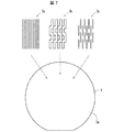
- FIG. 7 is a plan view showing the pattern shape of the mask.
- the mask material for forming the mask 6 may be a material other than SiO 2 , in which the semiconductor layer does not grow from the mask material due to vapor phase growth.
- Masking material for example, patterning can ZrO X, oxides such as TiO X or AlO X, or can be used transition metals such as W or Cr.
- a method suitable for the mask material such as a thin film deposition method, sputtering, or coating curing, can be appropriately used.
- a SiO 2 layer having a thickness of about 100 to 500 nm is formed.
- silicon oxide (SiO 2 ) which is a material for the mask 6, is laminated on the first surface 1a by a PCVD (Plasma Chemical Vapor Deposition) method or the like to have a thickness of about 100 to 500 nm.
- the mask pattern of the mask 6 may be a strip-shaped or striped shape indicated by reference numeral 7a in FIG. 7, or a grid pattern in which a plurality of strip-shaped bodies arranged so as to be orthogonal to each other in the vertical and horizontal directions shown by reference numeral 7b. Further, it may be a so-called repeat pattern (pattern) in which the openings 7 divided at regular intervals (repeat pitch), which are indicated by reference numerals 7c, are repeated a plurality of times.
- the edge region of the first surface 1a of the base substrate 1 near the end surface (side surface) 1c of the base substrate 1 is also covered with the above-mentioned mask 6 in consideration of the ease of peeling and separation of the semiconductor layer 3 described later. May be. As a result, the semiconductor layer near the edge located at the edge of the base substrate 1 can also be easily peeled off.
- the semiconductor device layer 8 obtained by growing the nitride semiconductor by the ELO method is obtained.
- the width of the semiconductor device layer 8 is, for example, about 50 ⁇ m to 200 ⁇ m, and the height is about 10 ⁇ m to 50 ⁇ m.
- the laser beam 5 may irradiate a region including a part of the base substrate 1 side or the base substrate 1 side of the connection portion 2.
- the laser beam 5 may be scanned in an arbitrary direction in the substrate surface of the substrate 1 by aligning the focus of the laser beam 5 with the position described above.
- another light source as described above may be used instead of the laser beam 5.
- the method of irradiating the connection portion 2 with the laser beam 5 in contact with the etching solution which is an electrolytic solution is a photoelectrochemical etching (also referred to as (Photo-electrochemical; PEC) etching).
- This PEC etching is a semiconductor.
- an "oxidation reaction” as represented by the following formula (1) and an “oxide film dissolution reaction” as represented by the formula (2) occur.
- "H + " in the formula (1) represents a hole.
- the connecting portion 2 When the connecting portion 2 is irradiated with the laser beam 5 in the etching solution 4 by the above-mentioned oxidation reaction and oxide film dissolution reaction, an electric field is generated from the inside of the connecting portion 2 toward the surface, and the connecting portion 2 is acid or alkaline from the surface. Dissolves or weakens in.
- the connecting portion 2 is weakened by irradiating the connecting portion 2 with a laser beam as described above.
- the base substrate 1 is taken out from the wafer bonding device, and the support substrate 10 is moved in a direction away from the base substrate 1.
- a large tensile stress is generated in the connecting portion 2 which is weakened by the irradiation of the laser beam 5, and the connecting portion 2 is broken as shown in FIG. 8C.
- the connection portion 2 since the connection portion 2 is in a fragile state or the like, the base substrate 1 can be easily separated. Separation can be done by an appropriate method. It is conceivable that the connection portion 2 remains on the base substrate 1 side, the semiconductor element 33 side, or both, depending on the vulnerable location. Therefore, after separation, the residue of the connecting portion 2 remaining on the semiconductor element 33 is removed by polishing or the like.
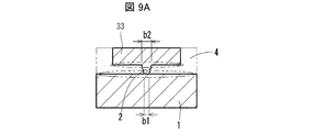
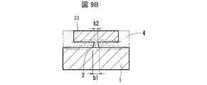
- FIGS. 9A to 9C are diagrams showing the etching shape of the connecting portion.
- the connecting portion 2 has a small width b1 on the base substrate 1 side, a large width b2 on the semiconductor element 33 side, and the cross section is etched in an inverted trapezoidal shape.
- the semiconductor device layer 8 is formed of a band-structured material that causes an energy barrier, for example, n-GaN / i-GaN / n-GaN. Then, a laser beam is irradiated to a selective region to cause photoexcitation, a current circuit, polarization due to electric field distortion, and the like. Thereby, the connection portion 2 or a part thereof can be selectively etched by an etchant such as KOH or TMAH which can accelerate the chemical etching reaction of the charge localized portion.
- an etchant such as KOH or TMAH which can accelerate the chemical etching reaction of the charge localized portion.
- the connecting portion 2 has a structure having pores by a VAS (Void-Assisted Separation) method, formation of a coarse initial nucleus, porosification by anodization, an In droplet method, or the like.
- VAS Vaid-Assisted Separation
- the surface area is increased and the rigidity is reduced as compared with the ELO structure having no pores.
- selective weakening is possible by increasing the etching rate.
- the width b2 on the semiconductor element 33 side of the connecting portion 2 is small, the width b1 on the base substrate 1 side is large, and the cross section can be etched into a trapezoidal shape.
- etching rate can be controlled by providing the above-mentioned multilayer structure inside the connecting portion 2.
- the method for manufacturing a semiconductor element of the present disclosure includes an element forming step of forming a semiconductor element located via a connecting portion on a base substrate, and irradiating light with the connecting portion in contact with an etching solution. It includes a light irradiation step of melting or weakening, and a separation step of separating the semiconductor element from the base substrate.
- the nitride semiconductor include GaN-based semiconductors, AlN (aluminum nitride), InAlN (indium nitride aluminum nitride), and InN (indium nitride).
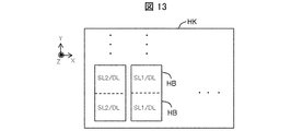
- the Z direction is the normal direction of the (0001) plane, which is the c-plane of the nitride semiconductor of the convex portion TS.
- the X direction is the normal direction of the (11-20) plane which is the a-plane of the nitride semiconductor of the convex portion TS, and the Y direction is the m-plane of the nitride semiconductor of the convex portion TS (1-100). The normal direction of the surface.
- the mask ML is located on the base substrate UK and includes the mask portions M1 and M2 and the openings K1 and K2 by the ELO (Epitaxial Lateral Overgrowth) method.
- the first semiconductor portion SL1 is formed, and then the mask portions M1 and M2 are etched and removed to form the hollow portion TK.
- the mask ML may be a mask layer.
- the convex portion TS is formed in the opening K1.
- the convex portion TS may have a shape in which the ⁇ 1-100> direction (Y direction) of the nitride semiconductor included therein is the longitudinal direction.
- the p-type semiconductor portion, the n-type semiconductor portion, the active portion, and the electrode portion are each formed in layers, and the device portion DL is formed by being laminated. That is, the device unit DL may be a device layer.
- the light emitting region can be formed so as to overlap the low dislocation portion WG in a plan view.
- FIG. 12 is a cross-sectional view showing a configuration example of the base substrate.
- the nitride semiconductor included in the convex portion TS is a GaN-based semiconductor
- the base substrate UK is on a dissimilar substrate MK having a lattice constant different from that of the GaN-based semiconductor of the convex portion TS and a dissimilar substrate MK. It may be configured to have a seed portion SD formed and containing a nitride semiconductor.
- the base substrate UK may be composed of a main substrate MK which is a silicon substrate and a seed portion SD (for example, an AlN portion), or a main substrate MK which is a silicon carbide substrate and a seed portion SD (for example, an AlN portion). , GaN-based semiconductor unit). Further, the base substrate UK includes a main substrate MK which is a silicon substrate, a buffer portion BF on the main substrate (including at least one of an AlN portion and a SiC portion), and a seed portion SD (for example, GaN) on the buffer portion. It may be composed of a system semiconductor unit). The base substrate UK may be a bulk type GaN substrate or a bulk type SiC substrate (hexagonal system) without being limited to these configurations. The seed portion SD may be the seed layer, and the buffer portion BF may be the buffer layer.
- the convex portion TS is irradiated with the laser beam LZ while the etching solution EH is brought into contact with the side surface of the convex portion TS, so that the anisotropy progresses from the side surface of the convex portion TS to the inside.
- Etching is performed.
- an oxide for example, Ga 2 O
- a nitride semiconductor for example, a GaN-based semiconductor
- an anion for example, hydroxide ion
- the step of separating the first semiconductor portion SL1 from the base substrate UK may be a step performed after the convex portion TS is weakened, or may be a step of crossing the convex portion TS.
- the laser beam LZ may be irradiated from the base substrate UK side or the support substrate SK side, but the latter is selected when the base substrate UK has a light-shielding property (for example, when a silicon substrate is included). ..
- the present disclosure has been described in detail above, but the present disclosure is not limited to the above-described embodiment, and various changes, improvements, etc. are made without departing from the gist of the present disclosure. Is possible.
- a base substrate having a material different from the semiconductor material contained in the semiconductor layer 3 is adopted. You may.
- the base substrate may be made of sapphire (Al 2 O 3 ), silicon carbide (SiC), silicon (Si), or the like.
- a buffer portion and a seed portion may be arranged on the base substrate.
- the example of irradiating the laser after removing the mask is described, but the mask may be removed after irradiating the laser and before peeling the semiconductor layer 3.
- Base substrate 1a One main surface (first surface) 1b The other main surface (second surface) 1c Side surface (third surface), end surface 2 Connection part 21 and 22 End part 23 Intermediate part 3
- Semiconductor layer 4 Etching solution 5 Laser light 6 Sedimentation suppression mask (mask) 6a Band 7 Opening 8 Semiconductor device layer 8a Top surface 8b Bottom surface 9
- Adhesive layer 10 Support substrate 10a Opposing surface 10b Bonding layer 33
- Semiconductor device 61 Opening G Gap (emission path) S semiconductor element a forming process a1 mask forming process a2 semiconductor layer forming process a3 mask removing process b weakening process c separation process c1 preparation process c2 joining process c3 peeling process S1 element forming process S2 light irradiation process S3 separation process
Landscapes
- Chemical & Material Sciences (AREA)
- Engineering & Computer Science (AREA)
- Physics & Mathematics (AREA)
- Optics & Photonics (AREA)
- Metallurgy (AREA)
- Organic Chemistry (AREA)
- Crystallography & Structural Chemistry (AREA)
- Materials Engineering (AREA)
- Chemical Kinetics & Catalysis (AREA)
- General Chemical & Material Sciences (AREA)
- Plasma & Fusion (AREA)
- Mechanical Engineering (AREA)
- Oil, Petroleum & Natural Gas (AREA)
- Inorganic Chemistry (AREA)
- Led Devices (AREA)
- Laser Beam Processing (AREA)
- Crystals, And After-Treatments Of Crystals (AREA)
- Mechanical Treatment Of Semiconductor (AREA)
- Recrystallisation Techniques (AREA)
- Semiconductor Lasers (AREA)
- Bipolar Transistors (AREA)
Priority Applications (5)
| Application Number | Priority Date | Filing Date | Title |
|---|---|---|---|
| EP21795307.4A EP4144896A4 (en) | 2020-04-28 | 2021-04-27 | METHOD FOR MANUFACTURING A SEMICONDUCTOR ELEMENT |
| US17/921,789 US20230170220A1 (en) | 2020-04-28 | 2021-04-27 | Manufacturing method of semiconductor element |
| JP2022518083A JPWO2021221055A1 (https=) | 2020-04-28 | 2021-04-27 | |
| CN202180030661.7A CN115443519B (zh) | 2020-04-28 | 2021-04-27 | 半导体元件的制造方法 |
| JP2024062912A JP7660742B2 (ja) | 2020-04-28 | 2024-04-09 | 半導体素子の製造方法および半導体デバイス |
Applications Claiming Priority (4)
| Application Number | Priority Date | Filing Date | Title |
|---|---|---|---|
| JP2020079547 | 2020-04-28 | ||
| JP2020-079547 | 2020-04-28 | ||
| JP2020110022 | 2020-06-25 | ||
| JP2020-110022 | 2020-06-25 |
Publications (1)
| Publication Number | Publication Date |
|---|---|
| WO2021221055A1 true WO2021221055A1 (ja) | 2021-11-04 |
Family
ID=78332095
Family Applications (1)
| Application Number | Title | Priority Date | Filing Date |
|---|---|---|---|
| PCT/JP2021/016802 Ceased WO2021221055A1 (ja) | 2020-04-28 | 2021-04-27 | 半導体素子の製造方法 |
Country Status (6)
| Country | Link |
|---|---|
| US (1) | US20230170220A1 (https=) |
| EP (1) | EP4144896A4 (https=) |
| JP (2) | JPWO2021221055A1 (https=) |
| CN (1) | CN115443519B (https=) |
| TW (1) | TWI813985B (https=) |
| WO (1) | WO2021221055A1 (https=) |
Cited By (5)
| Publication number | Priority date | Publication date | Assignee | Title |
|---|---|---|---|---|
| JPWO2022270309A1 (https=) * | 2021-06-21 | 2022-12-29 | ||
| JPWO2023153358A1 (https=) * | 2022-02-10 | 2023-08-17 | ||
| JPWO2023189872A1 (https=) * | 2022-03-28 | 2023-10-05 | ||
| WO2025070496A1 (ja) * | 2023-09-27 | 2025-04-03 | 京セラ株式会社 | 半導体基板並びにその製造方法および製造装置、半導体デバイス |
| WO2025095087A1 (ja) * | 2023-10-31 | 2025-05-08 | 京セラ株式会社 | 半導体基板、半導体基板の製造方法、半導体デバイスの製造方法、半導体デバイス、発光素子 |
Citations (7)
| Publication number | Priority date | Publication date | Assignee | Title |
|---|---|---|---|---|
| US20040014297A1 (en) * | 2002-07-17 | 2004-01-22 | National Chiao Tung University | Method for transferring epitaxy layer |
| JP2006060200A (ja) * | 2004-07-21 | 2006-03-02 | Nichia Chem Ind Ltd | 窒化物半導体ウエハ又は窒化物半導体素子の製造方法、それにより得られる窒化物半導体ウエハ又は窒化物半導体素子、並びにそれに用いるレーザ照射装置 |
| JP2007158100A (ja) * | 2005-12-06 | 2007-06-21 | Rohm Co Ltd | 窒化物半導体発光素子の製造方法 |
| JP4638958B1 (ja) | 2009-08-20 | 2011-02-23 | 株式会社パウデック | 半導体素子の製造方法 |
| JP2011079728A (ja) * | 2009-09-14 | 2011-04-21 | Sumitomo Electric Ind Ltd | 窒化物半導体エピタキシャル層の形成方法および窒化物半導体デバイスの製造方法 |
| JP2013021251A (ja) * | 2011-07-14 | 2013-01-31 | Toshiba Corp | 半導体発光素子の製造方法 |
| JP2019134101A (ja) * | 2018-01-31 | 2019-08-08 | 京セラ株式会社 | 半導体素子の製造方法 |
Family Cites Families (11)
| Publication number | Priority date | Publication date | Assignee | Title |
|---|---|---|---|---|
| EP0874405A3 (en) * | 1997-03-25 | 2004-09-15 | Mitsubishi Cable Industries, Ltd. | GaN group crystal base member having low dislocation density, use thereof and manufacturing methods thereof |
| JP4178936B2 (ja) * | 2002-12-11 | 2008-11-12 | 日本電気株式会社 | Iii族窒化物自立基板およびそれを用いた半導体素子ならびにそれらの製造方法 |
| JP4656410B2 (ja) * | 2005-09-05 | 2011-03-23 | 住友電気工業株式会社 | 窒化物半導体デバイスの製造方法 |
| JP2008311448A (ja) * | 2007-06-15 | 2008-12-25 | Mitsui Chemicals Inc | 有機トランジスタ |
| US8236583B2 (en) * | 2008-09-10 | 2012-08-07 | Tsmc Solid State Lighting Ltd. | Method of separating light-emitting diode from a growth substrate |
| JP5961557B2 (ja) * | 2010-01-27 | 2016-08-02 | イェイル ユニヴァーシティ | GaNデバイスのための導電率ベースの選択的エッチング及びその用途 |
| JP5146702B2 (ja) * | 2010-11-17 | 2013-02-20 | 住友電気工業株式会社 | 窒化物半導体デバイス |
| DE102012217644A1 (de) * | 2012-09-27 | 2014-03-27 | Osram Opto Semiconductors Gmbh | Optoelektronisches Bauelement |
| WO2019023281A1 (en) * | 2017-07-24 | 2019-01-31 | Microlink Devices, Inc. | DEEP PHOTOACTIVATED WET MATERIAL BURNING USING HIGH POWER ULTRAVIOLET LIGHT EMITTING DIODES |
| WO2019123954A1 (ja) * | 2017-12-21 | 2019-06-27 | パナソニックIpマネジメント株式会社 | 窒化物系薄膜複合構造体及びその製造方法 |
| CN112204754B (zh) * | 2018-05-30 | 2024-08-13 | 加利福尼亚大学董事会 | 从半导体衬底移除半导体层的方法 |
-
2021
- 2021-04-27 JP JP2022518083A patent/JPWO2021221055A1/ja active Pending
- 2021-04-27 EP EP21795307.4A patent/EP4144896A4/en active Pending
- 2021-04-27 US US17/921,789 patent/US20230170220A1/en active Pending
- 2021-04-27 CN CN202180030661.7A patent/CN115443519B/zh active Active
- 2021-04-27 WO PCT/JP2021/016802 patent/WO2021221055A1/ja not_active Ceased
- 2021-04-28 TW TW110115286A patent/TWI813985B/zh active
-
2024
- 2024-04-09 JP JP2024062912A patent/JP7660742B2/ja active Active
Patent Citations (7)
| Publication number | Priority date | Publication date | Assignee | Title |
|---|---|---|---|---|
| US20040014297A1 (en) * | 2002-07-17 | 2004-01-22 | National Chiao Tung University | Method for transferring epitaxy layer |
| JP2006060200A (ja) * | 2004-07-21 | 2006-03-02 | Nichia Chem Ind Ltd | 窒化物半導体ウエハ又は窒化物半導体素子の製造方法、それにより得られる窒化物半導体ウエハ又は窒化物半導体素子、並びにそれに用いるレーザ照射装置 |
| JP2007158100A (ja) * | 2005-12-06 | 2007-06-21 | Rohm Co Ltd | 窒化物半導体発光素子の製造方法 |
| JP4638958B1 (ja) | 2009-08-20 | 2011-02-23 | 株式会社パウデック | 半導体素子の製造方法 |
| JP2011079728A (ja) * | 2009-09-14 | 2011-04-21 | Sumitomo Electric Ind Ltd | 窒化物半導体エピタキシャル層の形成方法および窒化物半導体デバイスの製造方法 |
| JP2013021251A (ja) * | 2011-07-14 | 2013-01-31 | Toshiba Corp | 半導体発光素子の製造方法 |
| JP2019134101A (ja) * | 2018-01-31 | 2019-08-08 | 京セラ株式会社 | 半導体素子の製造方法 |
Non-Patent Citations (1)
| Title |
|---|
| See also references of EP4144896A4 |
Cited By (9)
| Publication number | Priority date | Publication date | Assignee | Title |
|---|---|---|---|---|
| JPWO2022270309A1 (https=) * | 2021-06-21 | 2022-12-29 | ||
| JP7637237B2 (ja) | 2021-06-21 | 2025-02-27 | 京セラ株式会社 | 半導体デバイスの製造方法および製造装置 |
| JPWO2023153358A1 (https=) * | 2022-02-10 | 2023-08-17 | ||
| WO2023153358A1 (ja) * | 2022-02-10 | 2023-08-17 | 京セラ株式会社 | レーザ素子の製造方法および製造装置 |
| EP4478563A4 (en) * | 2022-02-10 | 2025-06-11 | Kyocera Corporation | PRODUCTION DEVICE AND PRODUCTION METHOD FOR LASER ELEMENT |
| JP7813820B2 (ja) | 2022-02-10 | 2026-02-13 | 京セラ株式会社 | レーザ素子の製造方法および製造装置 |
| JPWO2023189872A1 (https=) * | 2022-03-28 | 2023-10-05 | ||
| WO2025070496A1 (ja) * | 2023-09-27 | 2025-04-03 | 京セラ株式会社 | 半導体基板並びにその製造方法および製造装置、半導体デバイス |
| WO2025095087A1 (ja) * | 2023-10-31 | 2025-05-08 | 京セラ株式会社 | 半導体基板、半導体基板の製造方法、半導体デバイスの製造方法、半導体デバイス、発光素子 |
Also Published As
| Publication number | Publication date |
|---|---|
| TWI813985B (zh) | 2023-09-01 |
| CN115443519B (zh) | 2025-09-02 |
| EP4144896A1 (en) | 2023-03-08 |
| EP4144896A4 (en) | 2024-07-10 |
| JPWO2021221055A1 (https=) | 2021-11-04 |
| JP7660742B2 (ja) | 2025-04-11 |
| JP2024118468A (ja) | 2024-08-30 |
| CN115443519A (zh) | 2022-12-06 |
| TW202205366A (zh) | 2022-02-01 |
| US20230170220A1 (en) | 2023-06-01 |
Similar Documents
| Publication | Publication Date | Title |
|---|---|---|
| JP7660742B2 (ja) | 半導体素子の製造方法および半導体デバイス | |
| TWI424588B (zh) | Semiconductor light emitting device manufacturing method | |
| JP4656410B2 (ja) | 窒化物半導体デバイスの製造方法 | |
| CN102326232B (zh) | 半导体元件的制造方法 | |
| US8163582B2 (en) | Method for fabricating a light emitting diode chip including etching by a laser beam | |
| TWI233216B (en) | Semiconductor element and method for producing the same | |
| JP5956604B2 (ja) | 発光ダイオード | |
| KR101454821B1 (ko) | 결정성막, 디바이스, 및, 결정성막 또는 디바이스의 제조방법 | |
| KR101087885B1 (ko) | 3족 질화물 반도체의 광전소자 제조방법 | |
| CN1965393A (zh) | 化合物半导体器件晶片的制造方法 | |
| JP2001085736A (ja) | 窒化物半導体チップの製造方法 | |
| JP2001176823A (ja) | 窒化物半導体チップの製造方法 | |
| JP2005109432A (ja) | Iii族窒化物系化合物半導体素子の製造方法 | |
| CN103548158A (zh) | 发光元件的制造方法以及发光元件 | |
| JP2025102870A (ja) | 大面積iii族窒化物結晶及び基板、その製造方法、並びにその使用方法 | |
| KR100788173B1 (ko) | 질화물 반도체 기판을 제조하는 방법 및 이를 이용한 3족질화물 반도체 발광소자를 제조하는 방법 | |
| JP2015144180A (ja) | Led素子製造用ウェハとその作製方法、およびled素子 | |
| KR20140014625A (ko) | 질화갈륨계 반도체 소자를 제조하는 방법 | |
| JP4834920B2 (ja) | 半導体素子の製造方法 | |
| JP2015144177A (ja) | Led素子製造用ウェハとその作製方法、およびled素子 | |
| JP5123331B2 (ja) | 窒化物半導体チップの製造方法および窒化物半導体チップ | |
| TW201914051A (zh) | 發光元件的製造方法 | |
| JP2008294343A (ja) | 窒化物系半導体レーザ素子の作製方法 |
Legal Events
| Date | Code | Title | Description |
|---|---|---|---|
| 121 | Ep: the epo has been informed by wipo that ep was designated in this application |
Ref document number: 21795307 Country of ref document: EP Kind code of ref document: A1 |
|
| ENP | Entry into the national phase |
Ref document number: 2022518083 Country of ref document: JP Kind code of ref document: A |
|
| NENP | Non-entry into the national phase |
Ref country code: DE |
|
| ENP | Entry into the national phase |
Ref document number: 2021795307 Country of ref document: EP Effective date: 20221128 |
|
| WWG | Wipo information: grant in national office |
Ref document number: 202180030661.7 Country of ref document: CN |