WO2021221055A1 - 半導体素子の製造方法 - Google Patents
半導体素子の製造方法 Download PDFInfo
- Publication number
- WO2021221055A1 WO2021221055A1 PCT/JP2021/016802 JP2021016802W WO2021221055A1 WO 2021221055 A1 WO2021221055 A1 WO 2021221055A1 JP 2021016802 W JP2021016802 W JP 2021016802W WO 2021221055 A1 WO2021221055 A1 WO 2021221055A1
- Authority
- WO
- WIPO (PCT)
- Prior art keywords
- semiconductor
- base substrate
- manufacturing
- substrate
- semiconductor element
- Prior art date
Links
Images


Classifications
-
- H—ELECTRICITY
- H01—ELECTRIC ELEMENTS
- H01L—SEMICONDUCTOR DEVICES NOT COVERED BY CLASS H10
- H01L21/00—Processes or apparatus adapted for the manufacture or treatment of semiconductor or solid state devices or of parts thereof
- H01L21/02—Manufacture or treatment of semiconductor devices or of parts thereof
- H01L21/02104—Forming layers
- H01L21/02365—Forming inorganic semiconducting materials on a substrate
- H01L21/02656—Special treatments
- H01L21/02664—Aftertreatments
-
- H—ELECTRICITY
- H01—ELECTRIC ELEMENTS
- H01L—SEMICONDUCTOR DEVICES NOT COVERED BY CLASS H10
- H01L21/00—Processes or apparatus adapted for the manufacture or treatment of semiconductor or solid state devices or of parts thereof
- H01L21/02—Manufacture or treatment of semiconductor devices or of parts thereof
- H01L21/04—Manufacture or treatment of semiconductor devices or of parts thereof the devices having at least one potential-jump barrier or surface barrier, e.g. PN junction, depletion layer or carrier concentration layer
- H01L21/18—Manufacture or treatment of semiconductor devices or of parts thereof the devices having at least one potential-jump barrier or surface barrier, e.g. PN junction, depletion layer or carrier concentration layer the devices having semiconductor bodies comprising elements of Group IV of the Periodic System or AIIIBV compounds with or without impurities, e.g. doping materials
- H01L21/30—Treatment of semiconductor bodies using processes or apparatus not provided for in groups H01L21/20 - H01L21/26
- H01L21/302—Treatment of semiconductor bodies using processes or apparatus not provided for in groups H01L21/20 - H01L21/26 to change their surface-physical characteristics or shape, e.g. etching, polishing, cutting
- H01L21/306—Chemical or electrical treatment, e.g. electrolytic etching
- H01L21/30604—Chemical etching
- H01L21/30612—Etching of AIIIBV compounds
- H01L21/30617—Anisotropic liquid etching
-
- B—PERFORMING OPERATIONS; TRANSPORTING
- B23—MACHINE TOOLS; METAL-WORKING NOT OTHERWISE PROVIDED FOR
- B23K—SOLDERING OR UNSOLDERING; WELDING; CLADDING OR PLATING BY SOLDERING OR WELDING; CUTTING BY APPLYING HEAT LOCALLY, e.g. FLAME CUTTING; WORKING BY LASER BEAM
- B23K26/00—Working by laser beam, e.g. welding, cutting or boring
- B23K26/0006—Working by laser beam, e.g. welding, cutting or boring taking account of the properties of the material involved
-
- B—PERFORMING OPERATIONS; TRANSPORTING
- B23—MACHINE TOOLS; METAL-WORKING NOT OTHERWISE PROVIDED FOR
- B23K—SOLDERING OR UNSOLDERING; WELDING; CLADDING OR PLATING BY SOLDERING OR WELDING; CUTTING BY APPLYING HEAT LOCALLY, e.g. FLAME CUTTING; WORKING BY LASER BEAM
- B23K26/00—Working by laser beam, e.g. welding, cutting or boring
- B23K26/02—Positioning or observing the workpiece, e.g. with respect to the point of impact; Aligning, aiming or focusing the laser beam
- B23K26/06—Shaping the laser beam, e.g. by masks or multi-focusing
- B23K26/062—Shaping the laser beam, e.g. by masks or multi-focusing by direct control of the laser beam
- B23K26/0622—Shaping the laser beam, e.g. by masks or multi-focusing by direct control of the laser beam by shaping pulses
- B23K26/0624—Shaping the laser beam, e.g. by masks or multi-focusing by direct control of the laser beam by shaping pulses using ultrashort pulses, i.e. pulses of 1ns or less
-
- B—PERFORMING OPERATIONS; TRANSPORTING
- B23—MACHINE TOOLS; METAL-WORKING NOT OTHERWISE PROVIDED FOR
- B23K—SOLDERING OR UNSOLDERING; WELDING; CLADDING OR PLATING BY SOLDERING OR WELDING; CUTTING BY APPLYING HEAT LOCALLY, e.g. FLAME CUTTING; WORKING BY LASER BEAM
- B23K26/00—Working by laser beam, e.g. welding, cutting or boring
- B23K26/50—Working by transmitting the laser beam through or within the workpiece
- B23K26/53—Working by transmitting the laser beam through or within the workpiece for modifying or reforming the material inside the workpiece, e.g. for producing break initiation cracks
-
- C—CHEMISTRY; METALLURGY
- C30—CRYSTAL GROWTH
- C30B—SINGLE-CRYSTAL GROWTH; UNIDIRECTIONAL SOLIDIFICATION OF EUTECTIC MATERIAL OR UNIDIRECTIONAL DEMIXING OF EUTECTOID MATERIAL; REFINING BY ZONE-MELTING OF MATERIAL; PRODUCTION OF A HOMOGENEOUS POLYCRYSTALLINE MATERIAL WITH DEFINED STRUCTURE; SINGLE CRYSTALS OR HOMOGENEOUS POLYCRYSTALLINE MATERIAL WITH DEFINED STRUCTURE; AFTER-TREATMENT OF SINGLE CRYSTALS OR A HOMOGENEOUS POLYCRYSTALLINE MATERIAL WITH DEFINED STRUCTURE; APPARATUS THEREFOR
- C30B25/00—Single-crystal growth by chemical reaction of reactive gases, e.g. chemical vapour-deposition growth
- C30B25/02—Epitaxial-layer growth
- C30B25/04—Pattern deposit, e.g. by using masks
-
- C—CHEMISTRY; METALLURGY
- C30—CRYSTAL GROWTH
- C30B—SINGLE-CRYSTAL GROWTH; UNIDIRECTIONAL SOLIDIFICATION OF EUTECTIC MATERIAL OR UNIDIRECTIONAL DEMIXING OF EUTECTOID MATERIAL; REFINING BY ZONE-MELTING OF MATERIAL; PRODUCTION OF A HOMOGENEOUS POLYCRYSTALLINE MATERIAL WITH DEFINED STRUCTURE; SINGLE CRYSTALS OR HOMOGENEOUS POLYCRYSTALLINE MATERIAL WITH DEFINED STRUCTURE; AFTER-TREATMENT OF SINGLE CRYSTALS OR A HOMOGENEOUS POLYCRYSTALLINE MATERIAL WITH DEFINED STRUCTURE; APPARATUS THEREFOR
- C30B25/00—Single-crystal growth by chemical reaction of reactive gases, e.g. chemical vapour-deposition growth
- C30B25/02—Epitaxial-layer growth
- C30B25/18—Epitaxial-layer growth characterised by the substrate
- C30B25/20—Epitaxial-layer growth characterised by the substrate the substrate being of the same materials as the epitaxial layer
-
- C—CHEMISTRY; METALLURGY
- C30—CRYSTAL GROWTH
- C30B—SINGLE-CRYSTAL GROWTH; UNIDIRECTIONAL SOLIDIFICATION OF EUTECTIC MATERIAL OR UNIDIRECTIONAL DEMIXING OF EUTECTOID MATERIAL; REFINING BY ZONE-MELTING OF MATERIAL; PRODUCTION OF A HOMOGENEOUS POLYCRYSTALLINE MATERIAL WITH DEFINED STRUCTURE; SINGLE CRYSTALS OR HOMOGENEOUS POLYCRYSTALLINE MATERIAL WITH DEFINED STRUCTURE; AFTER-TREATMENT OF SINGLE CRYSTALS OR A HOMOGENEOUS POLYCRYSTALLINE MATERIAL WITH DEFINED STRUCTURE; APPARATUS THEREFOR
- C30B29/00—Single crystals or homogeneous polycrystalline material with defined structure characterised by the material or by their shape
- C30B29/10—Inorganic compounds or compositions
- C30B29/40—AIIIBV compounds wherein A is B, Al, Ga, In or Tl and B is N, P, As, Sb or Bi
- C30B29/403—AIII-nitrides
- C30B29/406—Gallium nitride
-
- C—CHEMISTRY; METALLURGY
- C30—CRYSTAL GROWTH
- C30B—SINGLE-CRYSTAL GROWTH; UNIDIRECTIONAL SOLIDIFICATION OF EUTECTIC MATERIAL OR UNIDIRECTIONAL DEMIXING OF EUTECTOID MATERIAL; REFINING BY ZONE-MELTING OF MATERIAL; PRODUCTION OF A HOMOGENEOUS POLYCRYSTALLINE MATERIAL WITH DEFINED STRUCTURE; SINGLE CRYSTALS OR HOMOGENEOUS POLYCRYSTALLINE MATERIAL WITH DEFINED STRUCTURE; AFTER-TREATMENT OF SINGLE CRYSTALS OR A HOMOGENEOUS POLYCRYSTALLINE MATERIAL WITH DEFINED STRUCTURE; APPARATUS THEREFOR
- C30B33/00—After-treatment of single crystals or homogeneous polycrystalline material with defined structure
- C30B33/06—Joining of crystals
-
- H—ELECTRICITY
- H01—ELECTRIC ELEMENTS
- H01L—SEMICONDUCTOR DEVICES NOT COVERED BY CLASS H10
- H01L21/00—Processes or apparatus adapted for the manufacture or treatment of semiconductor or solid state devices or of parts thereof
- H01L21/02—Manufacture or treatment of semiconductor devices or of parts thereof
- H01L21/02104—Forming layers
- H01L21/02365—Forming inorganic semiconducting materials on a substrate
- H01L21/02367—Substrates
- H01L21/0237—Materials
- H01L21/02387—Group 13/15 materials
- H01L21/02389—Nitrides
-
- H—ELECTRICITY
- H01—ELECTRIC ELEMENTS
- H01L—SEMICONDUCTOR DEVICES NOT COVERED BY CLASS H10
- H01L21/00—Processes or apparatus adapted for the manufacture or treatment of semiconductor or solid state devices or of parts thereof
- H01L21/02—Manufacture or treatment of semiconductor devices or of parts thereof
- H01L21/02104—Forming layers
- H01L21/02365—Forming inorganic semiconducting materials on a substrate
- H01L21/02518—Deposited layers
- H01L21/02521—Materials
- H01L21/02538—Group 13/15 materials
- H01L21/0254—Nitrides
-
- H—ELECTRICITY
- H01—ELECTRIC ELEMENTS
- H01L—SEMICONDUCTOR DEVICES NOT COVERED BY CLASS H10
- H01L21/00—Processes or apparatus adapted for the manufacture or treatment of semiconductor or solid state devices or of parts thereof
- H01L21/02—Manufacture or treatment of semiconductor devices or of parts thereof
- H01L21/02104—Forming layers
- H01L21/02365—Forming inorganic semiconducting materials on a substrate
- H01L21/02612—Formation types
- H01L21/02617—Deposition types
- H01L21/02636—Selective deposition, e.g. simultaneous growth of mono- and non-monocrystalline semiconductor materials
- H01L21/02639—Preparation of substrate for selective deposition
- H01L21/02642—Mask materials other than SiO2 or SiN
-
- H—ELECTRICITY
- H01—ELECTRIC ELEMENTS
- H01L—SEMICONDUCTOR DEVICES NOT COVERED BY CLASS H10
- H01L21/00—Processes or apparatus adapted for the manufacture or treatment of semiconductor or solid state devices or of parts thereof
- H01L21/02—Manufacture or treatment of semiconductor devices or of parts thereof
- H01L21/02104—Forming layers
- H01L21/02365—Forming inorganic semiconducting materials on a substrate
- H01L21/02612—Formation types
- H01L21/02617—Deposition types
- H01L21/02636—Selective deposition, e.g. simultaneous growth of mono- and non-monocrystalline semiconductor materials
- H01L21/02647—Lateral overgrowth
-
- H—ELECTRICITY
- H01—ELECTRIC ELEMENTS
- H01L—SEMICONDUCTOR DEVICES NOT COVERED BY CLASS H10
- H01L21/00—Processes or apparatus adapted for the manufacture or treatment of semiconductor or solid state devices or of parts thereof
- H01L21/70—Manufacture or treatment of devices consisting of a plurality of solid state components formed in or on a common substrate or of parts thereof; Manufacture of integrated circuit devices or of parts thereof
- H01L21/77—Manufacture or treatment of devices consisting of a plurality of solid state components or integrated circuits formed in, or on, a common substrate
- H01L21/78—Manufacture or treatment of devices consisting of a plurality of solid state components or integrated circuits formed in, or on, a common substrate with subsequent division of the substrate into plural individual devices
- H01L21/7806—Manufacture or treatment of devices consisting of a plurality of solid state components or integrated circuits formed in, or on, a common substrate with subsequent division of the substrate into plural individual devices involving the separation of the active layers from a substrate
- H01L21/7813—Manufacture or treatment of devices consisting of a plurality of solid state components or integrated circuits formed in, or on, a common substrate with subsequent division of the substrate into plural individual devices involving the separation of the active layers from a substrate leaving a reusable substrate, e.g. epitaxial lift off
-
- H—ELECTRICITY
- H01—ELECTRIC ELEMENTS
- H01L—SEMICONDUCTOR DEVICES NOT COVERED BY CLASS H10
- H01L33/00—Semiconductor devices with at least one potential-jump barrier or surface barrier specially adapted for light emission; Processes or apparatus specially adapted for the manufacture or treatment thereof or of parts thereof; Details thereof
- H01L33/005—Processes
- H01L33/0062—Processes for devices with an active region comprising only III-V compounds
- H01L33/0075—Processes for devices with an active region comprising only III-V compounds comprising nitride compounds
-
- B—PERFORMING OPERATIONS; TRANSPORTING
- B23—MACHINE TOOLS; METAL-WORKING NOT OTHERWISE PROVIDED FOR
- B23K—SOLDERING OR UNSOLDERING; WELDING; CLADDING OR PLATING BY SOLDERING OR WELDING; CUTTING BY APPLYING HEAT LOCALLY, e.g. FLAME CUTTING; WORKING BY LASER BEAM
- B23K2101/00—Articles made by soldering, welding or cutting
- B23K2101/36—Electric or electronic devices
- B23K2101/40—Semiconductor devices
-
- B—PERFORMING OPERATIONS; TRANSPORTING
- B23—MACHINE TOOLS; METAL-WORKING NOT OTHERWISE PROVIDED FOR
- B23K—SOLDERING OR UNSOLDERING; WELDING; CLADDING OR PLATING BY SOLDERING OR WELDING; CUTTING BY APPLYING HEAT LOCALLY, e.g. FLAME CUTTING; WORKING BY LASER BEAM
- B23K2103/00—Materials to be soldered, welded or cut
- B23K2103/50—Inorganic material, e.g. metals, not provided for in B23K2103/02 – B23K2103/26
- B23K2103/56—Inorganic material, e.g. metals, not provided for in B23K2103/02 – B23K2103/26 semiconducting
-
- H—ELECTRICITY
- H01—ELECTRIC ELEMENTS
- H01L—SEMICONDUCTOR DEVICES NOT COVERED BY CLASS H10
- H01L21/00—Processes or apparatus adapted for the manufacture or treatment of semiconductor or solid state devices or of parts thereof
- H01L21/02—Manufacture or treatment of semiconductor devices or of parts thereof
- H01L21/04—Manufacture or treatment of semiconductor devices or of parts thereof the devices having at least one potential-jump barrier or surface barrier, e.g. PN junction, depletion layer or carrier concentration layer
- H01L21/18—Manufacture or treatment of semiconductor devices or of parts thereof the devices having at least one potential-jump barrier or surface barrier, e.g. PN junction, depletion layer or carrier concentration layer the devices having semiconductor bodies comprising elements of Group IV of the Periodic System or AIIIBV compounds with or without impurities, e.g. doping materials
- H01L21/26—Bombardment with radiation
- H01L21/263—Bombardment with radiation with high-energy radiation
- H01L21/268—Bombardment with radiation with high-energy radiation using electromagnetic radiation, e.g. laser radiation
-
- H—ELECTRICITY
- H01—ELECTRIC ELEMENTS
- H01L—SEMICONDUCTOR DEVICES NOT COVERED BY CLASS H10
- H01L21/00—Processes or apparatus adapted for the manufacture or treatment of semiconductor or solid state devices or of parts thereof
- H01L21/02—Manufacture or treatment of semiconductor devices or of parts thereof
- H01L21/04—Manufacture or treatment of semiconductor devices or of parts thereof the devices having at least one potential-jump barrier or surface barrier, e.g. PN junction, depletion layer or carrier concentration layer
- H01L21/18—Manufacture or treatment of semiconductor devices or of parts thereof the devices having at least one potential-jump barrier or surface barrier, e.g. PN junction, depletion layer or carrier concentration layer the devices having semiconductor bodies comprising elements of Group IV of the Periodic System or AIIIBV compounds with or without impurities, e.g. doping materials
- H01L21/30—Treatment of semiconductor bodies using processes or apparatus not provided for in groups H01L21/20 - H01L21/26
- H01L21/302—Treatment of semiconductor bodies using processes or apparatus not provided for in groups H01L21/20 - H01L21/26 to change their surface-physical characteristics or shape, e.g. etching, polishing, cutting
- H01L21/306—Chemical or electrical treatment, e.g. electrolytic etching
- H01L21/3063—Electrolytic etching
- H01L21/30635—Electrolytic etching of AIIIBV compounds
-
- H—ELECTRICITY
- H01—ELECTRIC ELEMENTS
- H01L—SEMICONDUCTOR DEVICES NOT COVERED BY CLASS H10
- H01L33/00—Semiconductor devices with at least one potential-jump barrier or surface barrier specially adapted for light emission; Processes or apparatus specially adapted for the manufacture or treatment thereof or of parts thereof; Details thereof
- H01L33/005—Processes
- H01L33/0062—Processes for devices with an active region comprising only III-V compounds
- H01L33/0066—Processes for devices with an active region comprising only III-V compounds with a substrate not being a III-V compound
- H01L33/007—Processes for devices with an active region comprising only III-V compounds with a substrate not being a III-V compound comprising nitride compounds
-
- H—ELECTRICITY
- H01—ELECTRIC ELEMENTS
- H01L—SEMICONDUCTOR DEVICES NOT COVERED BY CLASS H10
- H01L33/00—Semiconductor devices with at least one potential-jump barrier or surface barrier specially adapted for light emission; Processes or apparatus specially adapted for the manufacture or treatment thereof or of parts thereof; Details thereof
- H01L33/005—Processes
- H01L33/0093—Wafer bonding; Removal of the growth substrate
-
- H—ELECTRICITY
- H01—ELECTRIC ELEMENTS
- H01L—SEMICONDUCTOR DEVICES NOT COVERED BY CLASS H10
- H01L33/00—Semiconductor devices with at least one potential-jump barrier or surface barrier specially adapted for light emission; Processes or apparatus specially adapted for the manufacture or treatment thereof or of parts thereof; Details thereof
- H01L33/005—Processes
- H01L33/0095—Post-treatment of devices, e.g. annealing, recrystallisation or short-circuit elimination
-
- H—ELECTRICITY
- H01—ELECTRIC ELEMENTS
- H01S—DEVICES USING THE PROCESS OF LIGHT AMPLIFICATION BY STIMULATED EMISSION OF RADIATION [LASER] TO AMPLIFY OR GENERATE LIGHT; DEVICES USING STIMULATED EMISSION OF ELECTROMAGNETIC RADIATION IN WAVE RANGES OTHER THAN OPTICAL
- H01S2304/00—Special growth methods for semiconductor lasers
- H01S2304/12—Pendeo epitaxial lateral overgrowth [ELOG], e.g. for growing GaN based blue laser diodes
-
- H—ELECTRICITY
- H01—ELECTRIC ELEMENTS
- H01S—DEVICES USING THE PROCESS OF LIGHT AMPLIFICATION BY STIMULATED EMISSION OF RADIATION [LASER] TO AMPLIFY OR GENERATE LIGHT; DEVICES USING STIMULATED EMISSION OF ELECTROMAGNETIC RADIATION IN WAVE RANGES OTHER THAN OPTICAL
- H01S5/00—Semiconductor lasers
- H01S5/02—Structural details or components not essential to laser action
- H01S5/0206—Substrates, e.g. growth, shape, material, removal or bonding
- H01S5/0217—Removal of the substrate
-
- H—ELECTRICITY
- H01—ELECTRIC ELEMENTS
- H01S—DEVICES USING THE PROCESS OF LIGHT AMPLIFICATION BY STIMULATED EMISSION OF RADIATION [LASER] TO AMPLIFY OR GENERATE LIGHT; DEVICES USING STIMULATED EMISSION OF ELECTROMAGNETIC RADIATION IN WAVE RANGES OTHER THAN OPTICAL
- H01S5/00—Semiconductor lasers
- H01S5/20—Structure or shape of the semiconductor body to guide the optical wave ; Confining structures perpendicular to the optical axis, e.g. index or gain guiding, stripe geometry, broad area lasers, gain tailoring, transverse or lateral reflectors, special cladding structures, MQW barrier reflection layers
- H01S5/22—Structure or shape of the semiconductor body to guide the optical wave ; Confining structures perpendicular to the optical axis, e.g. index or gain guiding, stripe geometry, broad area lasers, gain tailoring, transverse or lateral reflectors, special cladding structures, MQW barrier reflection layers having a ridge or stripe structure
-
- H—ELECTRICITY
- H01—ELECTRIC ELEMENTS
- H01S—DEVICES USING THE PROCESS OF LIGHT AMPLIFICATION BY STIMULATED EMISSION OF RADIATION [LASER] TO AMPLIFY OR GENERATE LIGHT; DEVICES USING STIMULATED EMISSION OF ELECTROMAGNETIC RADIATION IN WAVE RANGES OTHER THAN OPTICAL
- H01S5/00—Semiconductor lasers
- H01S5/30—Structure or shape of the active region; Materials used for the active region
- H01S5/32—Structure or shape of the active region; Materials used for the active region comprising PN junctions, e.g. hetero- or double- heterostructures
- H01S5/323—Structure or shape of the active region; Materials used for the active region comprising PN junctions, e.g. hetero- or double- heterostructures in AIIIBV compounds, e.g. AlGaAs-laser, InP-based laser
- H01S5/32308—Structure or shape of the active region; Materials used for the active region comprising PN junctions, e.g. hetero- or double- heterostructures in AIIIBV compounds, e.g. AlGaAs-laser, InP-based laser emitting light at a wavelength less than 900 nm
- H01S5/32341—Structure or shape of the active region; Materials used for the active region comprising PN junctions, e.g. hetero- or double- heterostructures in AIIIBV compounds, e.g. AlGaAs-laser, InP-based laser emitting light at a wavelength less than 900 nm blue laser based on GaN or GaP
-
- H—ELECTRICITY
- H01—ELECTRIC ELEMENTS
- H01S—DEVICES USING THE PROCESS OF LIGHT AMPLIFICATION BY STIMULATED EMISSION OF RADIATION [LASER] TO AMPLIFY OR GENERATE LIGHT; DEVICES USING STIMULATED EMISSION OF ELECTROMAGNETIC RADIATION IN WAVE RANGES OTHER THAN OPTICAL
- H01S5/00—Semiconductor lasers
- H01S5/40—Arrangement of two or more semiconductor lasers, not provided for in groups H01S5/02 - H01S5/30
- H01S5/4025—Array arrangements, e.g. constituted by discrete laser diodes or laser bar
Definitions
- the present invention relates to a method for manufacturing a semiconductor device.
- Patent Document 1 In the method of manufacturing a semiconductor element, various techniques for separating a semiconductor layer formed on a substrate from the substrate have been proposed (see, for example, Patent Document 1 below).
- semiconductor layers adjacent to each other in the direction along the first surface are separated from each other at least partially in the direction along the first surface on the first surface of the base substrate.
- a separation step of separating the plurality of semiconductor layers from the base substrate is included.
- step a shows a forming step
- step b shows a weakening step
- step c shows a separation step
- step a1 shows a mask forming step
- step “a2” shows a semiconductor layer forming step
- step a3 shows a mask removing step.
- step c1 indicates a preparation step
- step c2 indicates a joining step
- step c3 indicates a peeling step.
- the method for manufacturing a semiconductor device of the present embodiment includes a forming step a, a fragility step b, and a separation step c.
- the forming step a is one of epitaxial vapor deposition, for example, by the selective lateral growth (ELO) method, each of which is connected to the base substrate 1 by the connecting portion 2 on the base substrate 1.
- ELO selective lateral growth
- This is a step of forming a plurality of semiconductor layers 3.
- the weakening step b is a step of irradiating the connecting portion 2 with the laser beam 5 to weaken the connecting portion 2.
- the separation step c is a step of separating the plurality of semiconductor layers 3 from the base substrate 1.
- Each semiconductor layer 3 has, for example, a cleavage plane, and further, electrodes, wiring conductors, and the like are arranged to form one or a plurality of semiconductor elements S.
- the semiconductor element S include, but are not limited to, a light emitting diode (Light Emitting Diode; LED), a semiconductor laser (Laser Diode; LD), a photodiode (Photodiode; PD), and the like.
- the base substrate 1 has a flat one main surface (hereinafter, also referred to as a first surface) 1a including a starting point of growth of a semiconductor crystal, and a flat other main surface (hereinafter, also referred to as a second surface) opposite to the first surface 1a. It has 1b and a side surface (hereinafter, also referred to as a third surface) 1c connecting the first surface 1a and the second surface 1b. At least the first surface 1a of the base substrate 1 is made of a nitride semiconductor.
- the base substrate 1 may be, for example, a substrate made of a nitride semiconductor such as gallium nitride (GaN), aluminum gallium nitride (AlGaN), or indium gallium nitride (InGaN).
- a nitride semiconductor such as gallium nitride (GaN), aluminum gallium nitride (AlGaN), or indium gallium nitride (InGaN).
- the base substrate 1 used in the present embodiment is a GaN substrate cut out from a GaN single crystal ingot.
- the base substrate 1 is cut out from the single crystal ingot so that the first surface 1a including the starting point of the growth of the semiconductor crystal is in a predetermined surface direction.
- the base substrate 1 may be an n-type substrate in which impurities such as Si are doped in GaN, or may be a p-type substrate in which impurities such as Mg are doped in GaN.
- the impurity density in the base substrate 1 is, for example, about 1 ⁇ 10 19 cm -3 or less.
- the forming step a is a step of forming a plurality of semiconductor layers 3 on the first surface 1a of the base substrate 1 by the ELO method.
- a plurality of semiconductor layers 3 are formed so that the semiconductor layers 3 adjacent to each other in the direction along the first surface 1a are separated from each other at least partially in the direction along the first surface 1a.
- the forming step a includes a mask forming step a1, a semiconductor layer forming step a2, and a mask removing step a3, which are shown below.
- the mask forming step a1 is a step of forming a deposition suppressing mask (hereinafter, also simply referred to as a mask) 6 that suppresses the crystals of semiconductor crystals on the base substrate 1.
- a deposition suppressing mask hereinafter, also simply referred to as a mask
- silicon oxide for example, SiO 2 or the like
- PCVD plasma chemical vapor deposition
- the silicon oxide layer is then patterned using, for example, a photolithography method and wet etching with Buffered Hydrogen Fluoride (BHF). In this way, the mask 6 is formed on the first surface 1a in a predetermined pattern.
- the mask 6 may have, for example, a striped shape in which a plurality of strip-shaped portions 61 are arranged in parallel at predetermined intervals.
- the width of the opening 62, which is also called a mask window, between two adjacent strips 61 is, for example, about 2 ⁇ m to 20 ⁇ m.
- the width of the strip 61 is, for example, about 50 ⁇ m to 200 ⁇ m.
- the edge region near the third surface 1c on the first surface 1a of the base substrate 1 may also be covered with the mask 6. This makes it possible to cleanly and surely separate the semiconductor layer 3 that grows in the edge region of the first surface 1a from the base substrate 1. Further, it is possible to suppress the abnormal growth of the semiconductor crystal in the edge region of the first surface 1a.
- A2 Semiconductor layer forming step
- a GaN crystal is vapor-deposited from a region of the first surface 1a of the base substrate 1 that is not covered by the mask 6 and is exposed to the opening 62. Let me.
- VPE vapor phase deposition
- MOCVD Metalorganic Chemical Vapor Deposition
- the semiconductor layer 3 is formed into a light emitting diode (LED) or a semiconductor laser (Laser Diode;). It can be formed as a multilayer film that functions as an LD) or the like.
- the semiconductor crystal When the grown semiconductor crystal exceeds the opening 62 of the mask 6, the semiconductor crystal also grows laterally along the upper surface of the mask 6.
- the growth of the semiconductor crystal may be terminated before the semiconductor crystal grown from the first surface 1a overlaps with the adjacent semiconductor crystal.
- a plurality of semiconductor layers 3 are obtained, each of which is connected to the first surface 1a by the connecting portion 2.
- the connecting portion 2 is made of, for example, a GaN crystal.
- the connecting portion 2 has, for example, a width of about 2 ⁇ m to 20 ⁇ m and a height of about 100 nm to 500 nm.
- Each semiconductor layer 3 has, for example, a width of about 50 ⁇ m to 200 ⁇ m and a height of about 10 ⁇ m to 50 ⁇ m.
- the growth of the semiconductor crystal may continue until the semiconductor crystal that grows laterally along the upper surface of the mask 6 overlaps with the adjacent semiconductor crystal. In this case, a semiconductor layer connected to the first surface 1a by a plurality of connecting portions 2 is obtained.
- the mask removing step a3 is a step of removing the mask 6 after the completion of the semiconductor layer forming step a2.
- the base substrate 1 on which the semiconductor layer 3 is formed is taken out from the vapor phase growth apparatus (epitaxial apparatus), and the mask 6 is removed using an etchant that does not substantially invade the semiconductor layer 3.
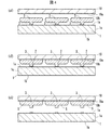
- the mask 6 when the mask 6 is made of a silicon oxide film, the mask 6 is removed by performing wet etching using BHF. In this way, for example, as shown in FIG. 1, a plurality of semiconductor layers 3 are obtained, each of which is connected to the first surface 1a by a connecting portion 2.
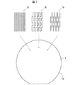
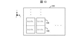
- Each of the plurality of semiconductor layers 3 may extend in a predetermined direction in a plan view. Further, the plurality of semiconductor layers 3 may form a pattern as shown in FIG. 3, for example, in a plan view. The plurality of semiconductor layers 3 may form a striped pattern extending in a predetermined direction, for example, as shown in FIG. 3A. As shown in FIG. 3B, for example, the plurality of semiconductor layers 3 may be arranged in a staggered pattern to form a so-called repeat pattern. As shown in FIG. 3C, for example, the plurality of semiconductor layers 3 may form a grid-like pattern in which each semiconductor layer 3 is connected to adjacent semiconductor layers 3 at both ends thereof.
- the weakening step b is a step of irradiating the connecting portion 2 with the laser beam 5 to weaken the connecting portion 2.
- the connection portion 2 can be thermally denatured and the crystal structure of the connection portion 2 can be changed by irradiating the laser beam 5.
- the connection portion 2 may be completely or partially cut by the irradiation of the laser beam 5.
- the wavelength of the laser beam 5 may be, for example, 370 nm or less.
- a light source that outputs the laser beam 5 for example, an AlGAN-based semiconductor laser, a KrF excimer laser, an ArF excimer laser, a YAG laser (third harmonic), or the like can be used.
- the focal length and spot size of the laser beam 5 can be appropriately selected according to the dimensions of the base substrate 1, the connecting portion 2, the semiconductor layer 3, and the like.
- the laser beam 5 may be irradiated from the first surface 1a side of the base substrate 1 or may be irradiated from the second surface 1b side of the base substrate 1.
- the laser beam 5 may be irradiated from the third surface 1c side of the base substrate 1.
- the separation step c is a step of separating a plurality of semiconductor layers 3 from the base substrate 1.
- a force is applied to the weakened connecting portion 2 by, for example, bringing the blade into contact with the semiconductor layer 3 or irradiating the connecting portion 2 with ultrasonic waves.
- the connection portion 2 can be broken and the semiconductor layer 3 can be separated from the base substrate 1.
- the separation step c can be omitted.
- the plurality of semiconductor layers 3 formed on the first surface 1a of the base substrate 1 include semiconductor layers 3 adjacent to each other in the direction along the first surface 1a. It is at least partially separated in the direction along the first surface 1a. Therefore, the decomposition product gas or the evaporation gas generated by irradiating the connection portion 2 with the laser beam 5 and filling the space between the semiconductor layer 3 and the base substrate 1 can be discharged to the outside.
- the gas can be released to the outside through, for example, a gap (hereinafter, also referred to as a release path) G between adjacent semiconductor layers 3 as shown by an arrow in FIG.
- the base substrate 1 can be reused without polishing for removing the damaged portion or by performing only a small amount of polishing. As a result, it is possible to improve the production efficiency of the semiconductor element S, and it is possible to provide the semiconductor element S that can increase the number of times that the base substrate 1 can be reused.
- the method for manufacturing a semiconductor element of the present embodiment it is not necessary to irradiate the entire base substrate 1 with the laser beam 5, and it is sufficient to irradiate only the connecting portion 2 connecting each semiconductor layer 3 and the first surface 1a. .. Therefore, it is possible to suppress excessive heating of the semiconductor layer 3 and the base substrate 1, and it is possible to reduce thermal damage to the semiconductor layer 3 and the base substrate 1. As a result, it becomes possible to manufacture a high-quality semiconductor element S. Further, the base substrate 1 can be reused without polishing for removing the damaged portion or by performing only a small amount of polishing. This makes it possible to improve the production efficiency of the semiconductor element S and reduce the manufacturing cost of the semiconductor element S.
- the base substrate 1, the connecting portion 2, and the semiconductor layer 3 are made of GaN crystals, their refractive indexes are substantially the same. Thereby, the refraction and reflection of the laser beam 5 at the interface between the base substrate 1 and the connecting portion 2 and the interface between the connecting portion 2 and the semiconductor layer 3 can be reduced. As a result, the laser beam 5 can be irradiated to the connection portion 2 with high accuracy and high efficiency. As a result, it becomes possible to manufacture a high-quality semiconductor element S. Further, the production efficiency of the semiconductor element S can be improved.
- the fragility step b is performed. Before this is performed, a through hole may be formed in the semiconductor layer so as to penetrate in the thickness direction thereof. As a result, the decomposition product gas or the evaporation gas that fills the space between the semiconductor layer and the base substrate 1 can be discharged to the outside through the through holes. As a result, even when the semiconductor layer connected to the first surface 1a is formed by the plurality of connecting portions 2, it becomes possible to manufacture the high-quality semiconductor element S and the production efficiency of the semiconductor element S. Can be improved.
- the laser beam 5 may be irradiated from the second surface 1b side of the base substrate 1 and incident on the base substrate 1 from the second surface 1b. Since the base substrate 1 is not a dissimilar substrate formed by forming a GaN layer on the surface of a sapphire substrate, a SiC substrate, or the like, but a substrate made of substantially the same material, the refractive index of the base substrate 1 is substantially constant. Therefore, by incident the laser light 5 from the second surface 1b of the base substrate 1, the laser light 5 can be focused on the connection portion 2 with high accuracy.
- connection portion 2 may be irradiated with picosecond pulse laser light or femtosecond pulse laser light.
- picosecond pulse laser light or femtosecond pulse laser light.
- an ablation phenomenon due to multiphoton absorption can be induced at the connection portion 2 which is the condensing point of the laser beam 5. Therefore, the connection portion 2 can be fragile with high accuracy while suppressing the occurrence of thermal damage in the semiconductor layer 3 and the base substrate 1.
- connection portion 2 may be irradiated with a sub-nanosecond pulse laser beam or a nanosecond pulse laser beam.
- the material removal rate is higher than in the case where the pulse width of the laser beam 5 is picoseconds or femtoseconds, so that the processing efficiency in the weakening step b can be improved.
- the decomposition product gas and the evaporation gas can be effectively emitted to the outside even when the pulse width of the laser beam 5 is sub-nanoseconds or nanoseconds.
- the optimization of the emission path G may be to form each semiconductor layer 3 so as to have a cross-sectional shape in which the corners of the lower surface are rounded, as shown in FIG. 1, for example.
- a plurality of semiconductor layers 3 arranged in a staggered pattern are formed, and the distance between the adjacent semiconductor layers 3 is set in two different directions. It may be to adjust.
- a scanning path that improves the production efficiency of the semiconductor element S may be selected according to the pattern shape of the plurality of semiconductor layers 3 formed on the base substrate 1. ..
- the laser beam 5 may be scanned from the outer peripheral portion to the central portion of the base substrate 1 while rotating the base substrate 1 around the axis perpendicular to the first surface 1a.
- the atmosphere, pressure, etc. in the laser processing apparatus are suppressed. May be adjusted. As a result, damage to the base substrate 1 due to oxidation can be reduced. As a result, the base substrate 1 can be reused without polishing to remove the damaged portion or by polishing only a small amount. This makes it possible to improve the production efficiency of the semiconductor element S and reduce the manufacturing cost of the semiconductor element S. Further, since it is possible to prevent the oxidized Ga metal from adhering to the semiconductor layer 3, it is possible to reduce the possibility that the quality of the semiconductor layer 3 is deteriorated. As a result, it becomes possible to manufacture a high-quality semiconductor element S.
- the focus of the laser beam 5 may be aligned with the end portion 21 of the connecting portion 2 on the base substrate 1 side.
- undesired thermal denaturation of the semiconductor layer 3 due to irradiation with the laser beam 5 can be suppressed.
- polishing for removing the heat-denatured portion of the semiconductor layer 3 can be omitted, or the amount of polishing of the semiconductor layer 3 can be reduced. As a result, it becomes possible to improve the production efficiency of the semiconductor element S.
- the focus of the laser beam 5 may be aligned with the end portion 22 of the connection portion 2 on the semiconductor layer 3 side.
- undesired thermal denaturation of the base substrate 1 due to irradiation with the laser beam 5 can be suppressed.
- polishing for removing the heat-denatured portion of the base substrate 1 can be omitted, or the amount of polishing of the base substrate 1 can be reduced.
- the production efficiency of the semiconductor element S can be improved and the manufacturing cost of the semiconductor element S can be reduced.
- the focus of the laser beam 5 may be aligned with the intermediate portion 23 located between the end portion of the connecting portion 2 on the base substrate 1 side and the end portion 22 on the 21 semiconductor layer 3 side.
- the intermediate portion 23 located between the end portion of the connecting portion 2 on the base substrate 1 side and the end portion 22 on the 21 semiconductor layer 3 side.
- the joining step c2 is a step of joining the support substrate 10 to the upper surfaces of the plurality of semiconductor layers 3.
- the support substrate 10 is arranged on the plurality of semiconductor layers 3 formed on the base substrate 1 in the forming step a.
- the support substrate 10 is arranged so that the facing surface 10a faces the first surface 1a of the base substrate 1.
- the support substrate 10 is heated while being pressed toward the base substrate 1, and the support substrate 10 is bonded to the upper surfaces of the plurality of semiconductor layers 3.
- the peeling step c3 is a step of peeling a plurality of semiconductor layers 3 from the base substrate 1.
- the base substrate 1 and the support substrate 10 are relatively separated from each other.
- tensile stress is generated in the connecting portion 2 which is weakened by the irradiation of the laser beam 5, and the connecting portion 2 is broken, so that the plurality of semiconductor layers 3 can be peeled off from the base substrate 1.
- the peeling step c3 may include a step of forming a cleavage plane on the semiconductor layer 3 and a step of forming an electrode, a wiring conductor, or the like on the semiconductor layer 3.
- the preparation step c1 and the joining step c2 may be performed between the forming step a and the weakening step b.
- the decomposition-generated gas or evaporative gas generated by the irradiation of the laser beam 5 flows in the space between the semiconductor layer 3 and the base substrate 1 along the first surface 1a toward the outer edge portion of the base substrate 1. , Released to the outside.
- the support substrate 10 may be formed with a gas flow path (not shown) for promoting the release of the decomposition product gas or the evaporative gas to the outside.
- the gas flow path may be, for example, a through hole that penetrates the support substrate 10 in the thickness direction.
- the gas flow path may be, for example, a groove formed on the facing surface 10a of the support substrate 10.
- semiconductor layers adjacent to each other in the direction along the first surface are separated from each other at least partially in the direction along the first surface on the first surface of the base substrate.
- a forming process that forms multiple semiconductor layers by epitaxial growth A fragility step of irradiating a connection portion between each of the plurality of semiconductor layers and the first surface with a laser beam to weaken the connection portion.
- a separation step of separating the plurality of semiconductor layers from the base substrate is included.
- the method for manufacturing a semiconductor element of the present disclosure it is possible to reduce damage to the base substrate and the semiconductor layer when the semiconductor layer is separated from the base substrate. This makes it possible to manufacture high-quality semiconductor devices and improve the production efficiency of semiconductor devices.
- the method for manufacturing a semiconductor device of the present embodiment includes an element forming step S1, a light irradiation step S2 (also referred to as a weakening step), and a separation step S3.
- the element forming step S1 is a step of forming the semiconductor element 33 coupled by the connecting portion 2 on the base substrate 1 by the ELO method.
- the light irradiation step S2 is a step of bringing the connecting portion 2 into contact with the etching solution 4 and irradiating at least a part of the connecting portion 2 with light such as a laser beam 5 to melt or weaken the connecting portion 2.
- the separation step S3 is a step of separating the semiconductor element 33 whose connecting portion 2 has been weakened by the light irradiation step S2 from the base substrate 1.
- the element forming step S1 and the light irradiation step S2 may not be performed in this order, and for example, the element forming step S1 and the light irradiation step S2 may be performed in parallel. As a result, the process time can be shortened.
- the semiconductor element 33 include, but are not limited to, a light emitting diode (Light Emitting Diode; LED), a semiconductor laser (Laser Diode; LD), and a photodiode (Photodiode; PD).
- the base substrate 1 has a first surface 1a which is a flat one main surface which is a starting point of crystal growth of a semiconductor, and a second surface 1b which is a flat other main surface on the back side thereof. At least the surface of the first surface 1a is a nitride semiconductor.
- the base substrate 1 used in the embodiment is, for example, a GaN substrate cut out from a single crystal ingot of gallium nitride (GaN) so that the first surface 1a, which is a growth surface, is in a predetermined surface direction.
- the GaN substrate may be either an n-type substrate or a p-type substrate in which impurities such as Si are doped in the semiconductor.
- the impurity density of the GaN substrate for example, one having an impurity density of about 1 ⁇ 10 19 cm -3 or less can be used.
- the base substrate 1 in addition to the GaN substrate, a substrate in which a GaN layer is formed on the surface of a substrate other than GaN such as a sapphire substrate and a SiC substrate may be used.
- the surface of the base substrate 1 is not limited to the GaN layer, and any substrate made of a GaN-based semiconductor can be used.
- the term "nitride semiconductor" refers those are constituted by Al x Ga y In z N ( 0 ⁇ x ⁇ 1,0 ⁇ y ⁇ 1,0 ⁇ z ⁇ 1,1).
- a mask 6 is formed on the above-mentioned base substrate 1.
- silicon oxide for example, SiO 2
- PCVD Physical Vapor Deposition
- the SiO 2 layer is patterned by a photolithography method and wet etching with buffered hydrofluoric acid (BHF) to form the mask 6 shown in FIG. 6A.
- the mask 6 has a striped shape in which a plurality of strip-shaped portions 6a are arranged in parallel at predetermined intervals.
- the width of the opening 7, which is also called a mask window, between two adjacent strips 6a is, for example, about 2 ⁇ m to 20 ⁇ m.
- the width of the band-shaped portion 6a is, for example, about 50 ⁇ m to 200 ⁇ m.
- FIG. 7 is a plan view showing the pattern shape of the mask.
- the mask material for forming the mask 6 may be a material other than SiO 2 , in which the semiconductor layer does not grow from the mask material due to vapor phase growth.
- Masking material for example, patterning can ZrO X, oxides such as TiO X or AlO X, or can be used transition metals such as W or Cr.
- a method suitable for the mask material such as a thin film deposition method, sputtering, or coating curing, can be appropriately used.
- a SiO 2 layer having a thickness of about 100 to 500 nm is formed.
- silicon oxide (SiO 2 ) which is a material for the mask 6, is laminated on the first surface 1a by a PCVD (Plasma Chemical Vapor Deposition) method or the like to have a thickness of about 100 to 500 nm.
- the mask pattern of the mask 6 may be a strip-shaped or striped shape indicated by reference numeral 7a in FIG. 7, or a grid pattern in which a plurality of strip-shaped bodies arranged so as to be orthogonal to each other in the vertical and horizontal directions shown by reference numeral 7b. Further, it may be a so-called repeat pattern (pattern) in which the openings 7 divided at regular intervals (repeat pitch), which are indicated by reference numerals 7c, are repeated a plurality of times.
- the edge region of the first surface 1a of the base substrate 1 near the end surface (side surface) 1c of the base substrate 1 is also covered with the above-mentioned mask 6 in consideration of the ease of peeling and separation of the semiconductor layer 3 described later. May be. As a result, the semiconductor layer near the edge located at the edge of the base substrate 1 can also be easily peeled off.
- the semiconductor device layer 8 obtained by growing the nitride semiconductor by the ELO method is obtained.
- the width of the semiconductor device layer 8 is, for example, about 50 ⁇ m to 200 ⁇ m, and the height is about 10 ⁇ m to 50 ⁇ m.
- the laser beam 5 may irradiate a region including a part of the base substrate 1 side or the base substrate 1 side of the connection portion 2.
- the laser beam 5 may be scanned in an arbitrary direction in the substrate surface of the substrate 1 by aligning the focus of the laser beam 5 with the position described above.
- another light source as described above may be used instead of the laser beam 5.
- the method of irradiating the connection portion 2 with the laser beam 5 in contact with the etching solution which is an electrolytic solution is a photoelectrochemical etching (also referred to as (Photo-electrochemical; PEC) etching).
- This PEC etching is a semiconductor.
- an "oxidation reaction” as represented by the following formula (1) and an “oxide film dissolution reaction” as represented by the formula (2) occur.
- "H + " in the formula (1) represents a hole.
- the connecting portion 2 When the connecting portion 2 is irradiated with the laser beam 5 in the etching solution 4 by the above-mentioned oxidation reaction and oxide film dissolution reaction, an electric field is generated from the inside of the connecting portion 2 toward the surface, and the connecting portion 2 is acid or alkaline from the surface. Dissolves or weakens in.
- the connecting portion 2 is weakened by irradiating the connecting portion 2 with a laser beam as described above.
- the base substrate 1 is taken out from the wafer bonding device, and the support substrate 10 is moved in a direction away from the base substrate 1.
- a large tensile stress is generated in the connecting portion 2 which is weakened by the irradiation of the laser beam 5, and the connecting portion 2 is broken as shown in FIG. 8C.
- the connection portion 2 since the connection portion 2 is in a fragile state or the like, the base substrate 1 can be easily separated. Separation can be done by an appropriate method. It is conceivable that the connection portion 2 remains on the base substrate 1 side, the semiconductor element 33 side, or both, depending on the vulnerable location. Therefore, after separation, the residue of the connecting portion 2 remaining on the semiconductor element 33 is removed by polishing or the like.
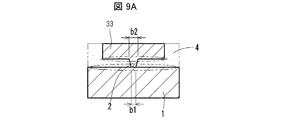
- FIGS. 9A to 9C are diagrams showing the etching shape of the connecting portion.
- the connecting portion 2 has a small width b1 on the base substrate 1 side, a large width b2 on the semiconductor element 33 side, and the cross section is etched in an inverted trapezoidal shape.
- the semiconductor device layer 8 is formed of a band-structured material that causes an energy barrier, for example, n-GaN / i-GaN / n-GaN. Then, a laser beam is irradiated to a selective region to cause photoexcitation, a current circuit, polarization due to electric field distortion, and the like. Thereby, the connection portion 2 or a part thereof can be selectively etched by an etchant such as KOH or TMAH which can accelerate the chemical etching reaction of the charge localized portion.
- an etchant such as KOH or TMAH which can accelerate the chemical etching reaction of the charge localized portion.
- the connecting portion 2 has a structure having pores by a VAS (Void-Assisted Separation) method, formation of a coarse initial nucleus, porosification by anodization, an In droplet method, or the like.
- VAS Vaid-Assisted Separation
- the surface area is increased and the rigidity is reduced as compared with the ELO structure having no pores.
- selective weakening is possible by increasing the etching rate.
- the width b2 on the semiconductor element 33 side of the connecting portion 2 is small, the width b1 on the base substrate 1 side is large, and the cross section can be etched into a trapezoidal shape.
- etching rate can be controlled by providing the above-mentioned multilayer structure inside the connecting portion 2.
- the method for manufacturing a semiconductor element of the present disclosure includes an element forming step of forming a semiconductor element located via a connecting portion on a base substrate, and irradiating light with the connecting portion in contact with an etching solution. It includes a light irradiation step of melting or weakening, and a separation step of separating the semiconductor element from the base substrate.
- the nitride semiconductor include GaN-based semiconductors, AlN (aluminum nitride), InAlN (indium nitride aluminum nitride), and InN (indium nitride).
- the Z direction is the normal direction of the (0001) plane, which is the c-plane of the nitride semiconductor of the convex portion TS.
- the X direction is the normal direction of the (11-20) plane which is the a-plane of the nitride semiconductor of the convex portion TS, and the Y direction is the m-plane of the nitride semiconductor of the convex portion TS (1-100). The normal direction of the surface.
- the mask ML is located on the base substrate UK and includes the mask portions M1 and M2 and the openings K1 and K2 by the ELO (Epitaxial Lateral Overgrowth) method.
- the first semiconductor portion SL1 is formed, and then the mask portions M1 and M2 are etched and removed to form the hollow portion TK.
- the mask ML may be a mask layer.
- the convex portion TS is formed in the opening K1.
- the convex portion TS may have a shape in which the ⁇ 1-100> direction (Y direction) of the nitride semiconductor included therein is the longitudinal direction.
- the p-type semiconductor portion, the n-type semiconductor portion, the active portion, and the electrode portion are each formed in layers, and the device portion DL is formed by being laminated. That is, the device unit DL may be a device layer.
- the light emitting region can be formed so as to overlap the low dislocation portion WG in a plan view.
- FIG. 12 is a cross-sectional view showing a configuration example of the base substrate.
- the nitride semiconductor included in the convex portion TS is a GaN-based semiconductor
- the base substrate UK is on a dissimilar substrate MK having a lattice constant different from that of the GaN-based semiconductor of the convex portion TS and a dissimilar substrate MK. It may be configured to have a seed portion SD formed and containing a nitride semiconductor.
- the base substrate UK may be composed of a main substrate MK which is a silicon substrate and a seed portion SD (for example, an AlN portion), or a main substrate MK which is a silicon carbide substrate and a seed portion SD (for example, an AlN portion). , GaN-based semiconductor unit). Further, the base substrate UK includes a main substrate MK which is a silicon substrate, a buffer portion BF on the main substrate (including at least one of an AlN portion and a SiC portion), and a seed portion SD (for example, GaN) on the buffer portion. It may be composed of a system semiconductor unit). The base substrate UK may be a bulk type GaN substrate or a bulk type SiC substrate (hexagonal system) without being limited to these configurations. The seed portion SD may be the seed layer, and the buffer portion BF may be the buffer layer.
- the convex portion TS is irradiated with the laser beam LZ while the etching solution EH is brought into contact with the side surface of the convex portion TS, so that the anisotropy progresses from the side surface of the convex portion TS to the inside.
- Etching is performed.
- an oxide for example, Ga 2 O
- a nitride semiconductor for example, a GaN-based semiconductor
- an anion for example, hydroxide ion
- the step of separating the first semiconductor portion SL1 from the base substrate UK may be a step performed after the convex portion TS is weakened, or may be a step of crossing the convex portion TS.
- the laser beam LZ may be irradiated from the base substrate UK side or the support substrate SK side, but the latter is selected when the base substrate UK has a light-shielding property (for example, when a silicon substrate is included). ..
- the present disclosure has been described in detail above, but the present disclosure is not limited to the above-described embodiment, and various changes, improvements, etc. are made without departing from the gist of the present disclosure. Is possible.
- a base substrate having a material different from the semiconductor material contained in the semiconductor layer 3 is adopted. You may.
- the base substrate may be made of sapphire (Al 2 O 3 ), silicon carbide (SiC), silicon (Si), or the like.
- a buffer portion and a seed portion may be arranged on the base substrate.
- the example of irradiating the laser after removing the mask is described, but the mask may be removed after irradiating the laser and before peeling the semiconductor layer 3.
- Base substrate 1a One main surface (first surface) 1b The other main surface (second surface) 1c Side surface (third surface), end surface 2 Connection part 21 and 22 End part 23 Intermediate part 3
- Semiconductor layer 4 Etching solution 5 Laser light 6 Sedimentation suppression mask (mask) 6a Band 7 Opening 8 Semiconductor device layer 8a Top surface 8b Bottom surface 9
- Adhesive layer 10 Support substrate 10a Opposing surface 10b Bonding layer 33
- Semiconductor device 61 Opening G Gap (emission path) S semiconductor element a forming process a1 mask forming process a2 semiconductor layer forming process a3 mask removing process b weakening process c separation process c1 preparation process c2 joining process c3 peeling process S1 element forming process S2 light irradiation process S3 separation process
Abstract
本開示の半導体素子の製造方法では、第1半導体部(SL1)が、下地基板(UK)に向けて突出する凸部(TS)を有し、凸部は窒化物半導体を含み、凸部と下地基板とが接合し、半導体基板(HK)は、下地基板および第1半導体部間に位置する中空部(TK)を有し、中空部は、凸部の側面に接し、かつ半導体基板の外部に通じており、第1半導体部を半導体基板から離隔する前に、凸部(TS)へのレーザ光(LZ)の照射を行う。
Description
本発明は、半導体素子の製造方法に関する。
半導体素子の製造方法において、基板上に形成された半導体層を基板から分離する技術が種々提案されている(例えば、下記の特許文献1を参照)。
本開示の半導体素子の製造方法は、下地基板の第1面に、前記第1面に沿った方向に隣り合う半導体層同士を前記第1面に沿った方向に少なくとも部分的に離隔させるように、エピタキシャル成長によって複数の半導体層を形成する形成工程と、前記複数の半導体層の各々と前記第1面との接続部にレーザ光を照射して、前記接続部を脆弱化する脆弱化工程と、前記複数の半導体層を前記下地基板から分離する分離工程と、を含む。
〔実施形態1〕
以下、本開示の実施形態1について、図面を参照しつつ説明する。図面は、図解を容易にするために、模式的に示されている。図1から図4を参照しながら説明する。
以下、本開示の実施形態1について、図面を参照しつつ説明する。図面は、図解を容易にするために、模式的に示されている。図1から図4を参照しながら説明する。
図1において、「工程a」は形成工程を示し、「工程b」は脆弱化工程を示し、「工程c」は分離工程を示す。図2において、「工程a1」はマスク形成工程を示し、工程「a2」は半導体層形成工程を示し、「工程a3」はマスク除去工程を示す。図4において、「工程c1」は準備工程を示し、「工程c2」は接合工程を示し、「工程c3」は剥離工程を示す。
本実施形態の半導体素子の製造方法は、形成工程aと、脆弱化工程bと、分離工程cと、を含む。形成工程aは、エピタキシャル気相成長の一つである、例えば選択横方向成長(Epitaxial Lateral Overgrowth;ELO)法によって、下地基板1上に、各々が接続部2によって下地基板1に接続された、複数の半導体層3を形成する工程である。また、脆弱化工程bは、接続部2にレーザ光5を照射して、接続部2を脆弱化する工程である。さらに、分離工程cは、複数の半導体層3を下地基板1から分離する工程である。
各半導体層3は、例えば、劈開面が形成され、さらに、電極、配線導体等が配置されて、1つまたは複数の半導体素子Sとなる。半導体素子Sとしては、例えば、発光ダイオード(Light Emitting Diode;LED)、半導体レーザ(Laser Diode;LD)、フォトダイオード(Photodiode;PD)等が挙げられるが、これらに限るものではない。
下地基板1は、半導体結晶の成長の起点を含む平坦な一方主面(以下、第1面ともいう)1a、第1面1aとは反対側の平坦な他方主面(以下、第2面ともいう)1b、および第1面1aと第2面1bとを接続する側面(以下、第3面ともいう)1cを有する。下地基板1は、少なくとも第1面1aが、窒化物半導体によって構成されている。下地基板1は、例えば、窒化ガリウム(GaN)、窒化アルミニウムガリウム(AlGaN)、窒化インジウムガリウム(InGaN)等の窒化物半導体から成る基板でよい。
本実施形態で使用する下地基板1は、GaN単結晶インゴットから切り出したGaN基板である。下地基板1は、半導体結晶の成長の起点を含む第1面1aが所定の面方向になるように、単結晶インゴットから切り出されている。下地基板1は、GaNにSiなどの不純物がドープされたn型基板であってもよく、GaNにMgなどの不純物がドープされたp型基板であってもよい。下地基板1における不純物密度は、例えば、1×1019cm-3程度以下である。
(a)形成工程
形成工程aは、ELO法によって、下地基板1の第1面1a上に複数の半導体層3を形成する工程である。形成工程aでは、第1面1aに沿った方向に隣り合う半導体層3同士を第1面1aに沿った方向に少なくとも部分的に離隔させるように、複数の半導体層3を形成する。
形成工程aは、ELO法によって、下地基板1の第1面1a上に複数の半導体層3を形成する工程である。形成工程aでは、第1面1aに沿った方向に隣り合う半導体層3同士を第1面1aに沿った方向に少なくとも部分的に離隔させるように、複数の半導体層3を形成する。
形成工程aは、以下に示す、マスク形成工程a1と、半導体層形成工程a2と、マスク除去工程a3とを含む。
(a1)マスク形成工程
マスク形成工程a1は、下地基板1上に、半導体結晶の結晶を抑制する堆積抑制マスク(以下、単に、マスクともいう)6を形成する工程である。マスク形成工程a1では、先ず、下地基板1の第1面1a上にマスク6の材料となる酸化シリコン(例えばSiO2等)を、プラズマ化学的気相成長(Plasma Chemical Vapor Deposition;PCVD)法等によって、第1面1a上に例えば100nm程度積層する。続いて、例えば、フォトリソグラフィー法とバッファードフッ酸(Buffered Hydrogen Fluoride;BHF)によるウェットエッチングとを用いて、酸化シリコン層をパターニングする。このようにして、第1面1a上にマスク6を所定のパターンで形成する。
マスク形成工程a1は、下地基板1上に、半導体結晶の結晶を抑制する堆積抑制マスク(以下、単に、マスクともいう)6を形成する工程である。マスク形成工程a1では、先ず、下地基板1の第1面1a上にマスク6の材料となる酸化シリコン(例えばSiO2等)を、プラズマ化学的気相成長(Plasma Chemical Vapor Deposition;PCVD)法等によって、第1面1a上に例えば100nm程度積層する。続いて、例えば、フォトリソグラフィー法とバッファードフッ酸(Buffered Hydrogen Fluoride;BHF)によるウェットエッチングとを用いて、酸化シリコン層をパターニングする。このようにして、第1面1a上にマスク6を所定のパターンで形成する。
マスク6は、例えば、帯状部61を所定の間隔で複数本平行に並べたストライプ状であってもよい。隣り合う2つの帯状部61の間の、マスクウィンドウとも称される開口部62の幅は、例えば2μmから20μm程度である。帯状部61の幅は、例えば50μmから200μm程度である。
下地基板1の第1面1aにおける、第3面1c近傍の縁部領域も、マスク6によって覆われていてもよい。これにより、第1面1aの縁部領域に成長する半導体層3を、下地基板1からきれいに確実に分離することが可能になる。さらに、第1面1aの縁部領域に半導体結晶が異常成長することを抑制できる。
(a2)半導体層形成工程
半導体層形成工程a2では、下地基板1の第1面1aにおける、マスク6に覆われておらず、開口部62に露出している領域から、GaN結晶を気相成長させる。
半導体層形成工程a2では、下地基板1の第1面1aにおける、マスク6に覆われておらず、開口部62に露出している領域から、GaN結晶を気相成長させる。
半導体結晶を成長させるための方法として、例えば、III族原料に塩化物を用いる塩化物輸送法による気相成長(Vapor Phase Epitaxy;VPE)、またはIII族原料に有機金属を用いる有機金属化学蒸着(Metal Organic Chemical Vapor Deposition;MOCVD)を用いることができる。例えば、GaN結晶の成長中にIII族元素の原料ガスの割合、不純物の原料ガスの割合等を変化させることによって、半導体層3を発光ダイオード(Light Emitting Diode;LED)または半導体レーザ(Laser Diode;LD)等として機能する多層膜として形成することができる。
成長した半導体結晶がマスク6の開口部62を超えると、マスク6の上面に沿って横方向にも半導体結晶が成長する。半導体結晶の成長は、第1面1aから成長した半導体結晶が、隣り合う半導体結晶と互いに重なる前に終了させてもよい。このようにして、例えば図1,2に示すように、各々が接続部2によって第1面1aに接続された、複数の半導体層3を得る。接続部2は、半導体層3と同様に、例えばGaN結晶から成る。接続部2は、例えば、幅が2μmから20μm程度であり、高さが100nmから500nm程度である。各半導体層3は、例えば、幅が50μmから200μm程度であり、高さが10μmから50μm程度である。半導体結晶の成長は、マスク6の上面に沿って横方向に成長する半導体結晶が、隣り合う半導体結晶と重なるまで継続してもよい。この場合、複数の接続部2によって第1面1aに接続された半導体層を得る。
(a3)マスク除去工程
マスク除去工程a3は、半導体層形成工程a2の完了後、マスク6を除去する工程である。マスク除去工程a3では、半導体層3が形成された下地基板1を気相成長装置(エピタキシャル装置)から取り出し、半導体層3を実質的に侵さないエッチャントを用いて、マスク6を除去する。
マスク除去工程a3は、半導体層形成工程a2の完了後、マスク6を除去する工程である。マスク除去工程a3では、半導体層3が形成された下地基板1を気相成長装置(エピタキシャル装置)から取り出し、半導体層3を実質的に侵さないエッチャントを用いて、マスク6を除去する。
例えば、マスク6が酸化シリコン膜から成る場合、BHFを用いたウェットエッチングを行って、マスク6を除去する。このようにして、例えば図1に示すように、各々が接続部2によって第1面1aと接続された、複数の半導体層3が得られる。
複数の半導体層3の各々は、平面視において、所定の方向に延びていてもよい。また、複数の半導体層3は、平面視において、例えば図3に示すようなパターンを形成してもよい。複数の半導体層3は、例えば図3(a)に示すように、所定の方向に延びるストライプ状のパターンを形成してもよい。複数の半導体層3は、例えば図3(b)に示すように、千鳥状に配列され、所謂、リピート柄パターンを形成してもよい。複数の半導体層3は、例えば図3(c)に示すように、各半導体層3が、その両端部において、隣り合う半導体層3と接続されている格子状のパターンを形成してもよい。
(b)脆弱化工程
脆弱化工程bは、接続部2にレーザ光5を照射して、接続部2を脆弱化する工程である。脆弱化工程bでは、レーザ光5の照射によって、例えば、接続部2を熱変性させ、接続部2の結晶構造を変化させることができる。これにより、例えば、接続部2にクラック、割れ等を生じさせ、接続部2の機械的強度を低下させることができる。脆弱化工程bでは、レーザ光5の照射によって、接続部2を完全に、または部分的に切断してもよい。
脆弱化工程bは、接続部2にレーザ光5を照射して、接続部2を脆弱化する工程である。脆弱化工程bでは、レーザ光5の照射によって、例えば、接続部2を熱変性させ、接続部2の結晶構造を変化させることができる。これにより、例えば、接続部2にクラック、割れ等を生じさせ、接続部2の機械的強度を低下させることができる。脆弱化工程bでは、レーザ光5の照射によって、接続部2を完全に、または部分的に切断してもよい。
レーザ光5の波長は、例えば、370nm以下であってもよい。レーザ光5を出力する光源としては、例えば、AlGAN系半導体レーザ、KrFエキシマレーザ、ArFエキシマレーザ、YAGレーザ(第三高調波)等を用いることができる。レーザ光5の焦点距離およびスポットサイズは、下地基板1、接続部2および半導体層3の寸法等に応じて、適宜選択することができる。
レーザ光5は、下地基板1の第1面1a側から照射されてもよく、下地基板1の第2面1b側から照射されてもよい。レーザ光5は、下地基板1の第3面1c側から照射されてもよい。
(c)分離工程
分離工程cは、複数の半導体層3を下地基板1から分離する工程である。分離工程cでは、例えば、半導体層3にブレードを当接させる、または接続部2に超音波を照射する等して、脆弱化された接続部2に力を加える。これにより、接続部2を破断し、半導体層3を下地基板1から分離することができる。
分離工程cは、複数の半導体層3を下地基板1から分離する工程である。分離工程cでは、例えば、半導体層3にブレードを当接させる、または接続部2に超音波を照射する等して、脆弱化された接続部2に力を加える。これにより、接続部2を破断し、半導体層3を下地基板1から分離することができる。
脆弱化工程bにおいて、接続部2をレーザ光5の照射によって完全に切断する場合には、分離工程cを省略することができる。
本実施形態の半導体素子の製造方法によれば、下地基板1の第1面1a上に形成される複数の半導体層3は、第1面1aに沿った方向に隣り合う半導体層3同士が、第1面1aに沿った方向に少なくとも部分的に離隔している。このため、接続部2へのレーザ光5の照射によって発生し、半導体層3と下地基板1との間の空間に充満する分解生成ガスまたは蒸発ガスなどを外部に放出することができる。ガスの外部への放出は、例えば図1において矢印で示すように、隣り合う半導体層3同士の間の間隙(以下、放出経路ともいう)Gを介して行うことができる。これにより、分解生成ガスまたは蒸発ガスなどの圧力による半導体層3および下地基板1の損傷を低減することができる。その結果、高品質の半導体素子Sを製造することが可能になる。また、下地基板1は、損傷した部位を除去するための研磨を行うことなく、あるいは、少量の研磨だけを行って、再使用することができる。これにより、半導体素子Sの生産効率を向上させることが可能になるとともに、下地基板1の再使用可能回数を増加させ得る半導体素子Sを提供できる。
また、本実施形態の半導体素子の製造方法では、レーザ光5を下地基板1全体に照射する必要はなく、各半導体層3と第1面1aとを接続する接続部2だけに照射すればよい。このため、半導体層3および下地基板1が過度に加熱されることを抑制でき、半導体層3および下地基板1の熱的損傷を低減することができる。その結果、高品質の半導体素子Sを製造することが可能になる。また、下地基板1は、損傷した部位を除去するための研磨を行うことなく、あるいは、少量の研磨だけを行って、再使用することができる。これにより、半導体素子Sの生産効率の向上および半導体素子Sの製造コストの低減が可能になる。
また、本実施形態の半導体素子の製造方法では、下地基板1、接続部2および半導体層3は、GaN結晶から成るため、それらの屈折率は、実質的に、同一である。これにより、下地基板1と接続部2との界面、および接続部2と半導体層3との界面におけるレーザ光5の屈折および反射を低減することができる。その結果、レーザ光5を高精度かつ高効率に接続部2に照射することができる。ひいては、高品質の半導体素子Sを製造することが可能になる。また、半導体素子Sの生産効率の向上が可能になる。
半導体層形成工程a2において、半導体結晶の成長を隣り合う半導体結晶同士が互いに重なるまで継続し、複数の接続部2によって第1面1aに接続された半導体層を形成する場合、脆弱化工程bを行う前に、該半導体層に、その厚み方向に貫通する貫通孔を形成しておいてもよい。これにより、半導体層と下地基板1との間の空間に充満する分解生成ガスまたは蒸発ガスを、貫通孔を介して、外部に放出することができる。その結果、複数の接続部2によって第1面1aに接続された半導体層を形成する場合であっても、高品質の半導体素子Sを製造することが可能になるとともに、半導体素子Sの生産効率の向上が可能になる。
脆弱化工程bでは、レーザ光5を、下地基板1の第2面1b側から照射し、第2面1bから下地基板1に入射させてもよい。下地基板1は、サファイア基板、SiC基板等の表面にGaN層を形成して成る異種基板ではなく、概略同一材料から成る基板であるため、下地基板1の屈折率が実質的に一定である。このため、レーザ光5を下地基板1の第2面1bから入射させることによって、レーザ光5を接続部2に高精度に集光することができる。また、レーザ光5を半導体層3が形成されていない第2面1b側から照射することによって、レーザ光5の照射が半導体層3を変性させる虞を低減できる。さらに、下地基板1の屈折率が実質的に一定であるため、レーザ光5を接続部2に集光するための光学系として、簡易な構成のレンズ光学系を使用することができる。これにより、半導体素子Sの生産効率を向上させることができる。なお、本記載は、本開示において、サファイア基板、SiC基板などの異種基板が、下地基板1として採用されることを排除するものではない。
脆弱化工程bでは、接続部2にピコ秒パルスレーザ光またはフェムト秒パルスレーザ光を照射してもよい。これにより、レーザ光5の集光点である接続部2において、多光子吸収によるアブレーション現象を誘起することができる。このため、半導体層3および下地基板1における熱的損傷の発生を抑制しつつ、接続部2を高精度に脆弱化することができる。
脆弱化工程bでは、接続部2にサブナノ秒パルスレーザ光またはナノ秒パルスレーザ光を照射してもよい。これにより、レーザ光5のパルス幅がピコ秒またはフェムト秒である場合と比較して、材料除去率が高くなるため、脆弱化工程bにおける加工効率を向上させることができる。
レーザ光5のパルス幅がサブナノ秒またはナノ秒である場合、レーザ光5のパルス幅がピコ秒またはフェムト秒である場合と比較して、多量の分解生成ガスまたは蒸発ガスが発生することがある。放出経路Gを最適化することによって、レーザ光5のパルス幅がサブナノ秒またはナノ秒である場合であっても、分解生成ガスおよび蒸発ガスを外部に効果的に放出することが可能になる。放出経路Gの最適化は、例えば図1に示すように、各半導体層3を、下面の角部が丸められている断面形状を有するように形成することであってもよい。放出経路Gの最適化は、例えば図3(b)に示すように、千鳥状に配列された複数の半導体層3を形成し、互いに異なる2つの方向において、隣り合う半導体層3同士の間隔を調整することであってもよい。
脆弱化工程bにおけるレーザ光5の走査経路は、下地基板1上に形成された複数の半導体層3のパターン形状等に応じて、半導体素子Sの生産効率が向上する走査経路を選択すればよい。脆弱化工程bでは、例えば、下地基板1を第1面1aに垂直な軸線の回りに回転させながら、レーザ光5を下地基板1の外周部から中央部に向かって走査してもよい。これにより、レーザ光5の集光点を複数回往復させる必要がなくなるため、脆弱化工程bに要する時間を短縮することができる。ひいては、半導体素子Sの生産効率を向上させることができる。
脆弱化工程bでは、下地基板1を加熱することによって、下地基板1の温度を所定の温度範囲内に維持してもよい。これにより、レーザ光5の照射により析出したGa金属を溶融状態とし、半導体層3に固着しにくくさせる。これにより、半導体層3の品質を維持することができる。所定の温度範囲は、例えば、室温付近(15℃から35℃程度)以上300℃以下であってよい。
脆弱化工程bでは、レーザ光5の照射により高温度となる下地基板1の酸化、およびレーザ光5の照射により析出したGa金属の酸化を抑制するために、レーザ加工装置内の雰囲気、圧力等を調整してもよい。これにより、酸化による下地基板1の損傷を低減することができる。その結果、下地基板1は、損傷した部位を除去するための研磨を行うことなく、あるいは、少量の研磨だけを行って、再使用することができる。これにより、半導体素子Sの生産効率の向上および半導体素子Sの製造コストの低減が可能になる。また、酸化したGa金属が半導体層3に付着することを抑制できるため、半導体層3の品質が低下する虞を低減することができる。その結果、高品質の半導体素子Sを製造することが可能になる。
脆弱化工程bでは、レーザ光5の焦点を、接続部2の下地基板1側の端部21に合わせてもよい。これにより、レーザ光5の照射による半導体層3の不所望な熱変性を抑制することができる。その結果、半導体層3における熱変性した部位を除去するための研磨を省略することができる、または、半導体層3を研磨する量を低減することができる。ひいては、半導体素子Sの生産効率を向上させることが可能になる。
脆弱化工程bでは、レーザ光5の焦点を、接続部2の半導体層3側の端部22に合わせてもよい。これにより、レーザ光5の照射による下地基板1の不所望な熱変性を抑制できる。その結果、下地基板1における熱変性した部位を除去するための研磨を省略することができる、または、下地基板1を研磨する量を低減することができる。ひいては、半導体素子Sの生産効率の向上および半導体素子Sの製造コストの低減が可能になる。
脆弱化工程bでは、レーザ光5の焦点を、接続部2の下地基板1側の端部と21半導体層3側の端部22との間に位置する中間部23に合わせてもよい。これにより、これにより、半導体層3および下地基板1の不所望な熱変性を抑制することができる。その結果、高品質の半導体素子Sを製造することが可能とともに、半導体素子Sの生産効率の向上および半導体素子Sの製造コストの低減が可能になる。
脆弱化工程bにおいて、接続部2を完全に切断しない場合、分離工程cは、準備工程c1と、接合工程c2と、剥離工程c3とを含んでもよい。
準備工程c1は、下地基板1の第1面1aと対向させる対向面10aを有する支持基板10を準備する工程である。支持基板10は、対向面10aに、AuSn等の材料を用いた半田からなる接合層10bを有している。
接合工程c2は、複数の半導体層3の上面に支持基板10を接合する工程である。接合工程c2では、先ず、形成工程aで下地基板1上に形成された複数の半導体層3の上に支持基板10を配置する。支持基板10は、対向面10aが下地基板1の第1面1aに対向するように配置される。続いて、支持基板10を下地基板1側に押圧しながら加熱し、複数の半導体層3の上面に支持基板10を接合する。
剥離工程c3は、複数の半導体層3を下地基板1から剥離する工程である。剥離工程c3では、下地基板1と支持基板10とを相対的に離隔させる。これにより、レーザ光5の照射によって脆弱化されている接続部2に引張応力が発生し、接続部2が破断するので、複数の半導体層3を下地基板1から剥離することができる。接続部2を脆弱化しておくことによって、複数の半導体層3を、それらを損傷させることなく、下地基板1から剥離することができる。剥離工程c3は、半導体層3に劈開面を形成する工程、および半導体層3に電極、配線導体等を形成する工程を含んでいてもよい。
なお、準備工程c1および接合工程c2は、形成工程aと脆弱化工程bとの間に行ってもよい。この場合、レーザ光5の照射によって生じる分解生成ガスまたは蒸発ガスは、半導体層3と下地基板1との間の空間を、第1面1aに沿って、下地基板1の外縁部に向かって流れ、外部に放出される。支持基板10には、分解生成ガスまたは蒸発ガスの外部への放出を促進するためのガス流路(図示せず)が形成されていてもよい。ガス流路は、例えば、支持基板10を厚み方向に貫通する貫通孔であってもよい。ガス流路は、例えば、支持基板10の対向面10aに形成される溝部であってもよい。
本開示の半導体素子の製造方法は、下地基板の第1面に、前記第1面に沿った方向に隣り合う半導体層同士を前記第1面に沿った方向に少なくとも部分的に離隔させるように、エピタキシャル成長によって複数の半導体層を形成する形成工程と、
前記複数の半導体層の各々と前記第1面との接続部にレーザ光を照射して、前記接続部を脆弱化する脆弱化工程と、
前記複数の半導体層を前記下地基板から分離する分離工程と、を含む。
前記複数の半導体層の各々と前記第1面との接続部にレーザ光を照射して、前記接続部を脆弱化する脆弱化工程と、
前記複数の半導体層を前記下地基板から分離する分離工程と、を含む。
品質の良好な半導体素子を製造するために、半導体層を基板から分離する方法には改善の余地がある。
本開示の半導体素子の製造方法によれば、半導体層を下地基板から分離する際の、下地基板および半導体層の損傷を低減することができる。これにより、高品質の半導体素子を製造することが可能になるとともに、半導体素子の生産効率の向上が可能になる。
〔実施形態2〕
以下、本開示に係る他の実施形態について、模式的に示した各図を参照しつつ説明する。
以下、本開示に係る他の実施形態について、模式的に示した各図を参照しつつ説明する。
本実施形態の半導体素子の製造方法は、図5に示されるように、素子形成工程S1と、光照射工程S2(または脆弱化工程ともいう)と、分離工程S3とを含む。また、図6A、図6Bおよび図6Cに示されるように、素子形成工程S1は、下地基板1上に、接続部2によって結合された半導体素子33をELO法によって形成する工程である。光照射工程S2は、接続部2をエッチング溶液4に接触させるとともに、接続部2の少なくとも一部に対してレーザ光5などの光を照射して、接続部2を溶かすかまたは脆弱化する工程である。分離工程S3は、光照射工程S2によって接続部2が脆弱化などされた半導体素子33を、下地基板1から分離する工程である。
素子形成工程S1および光照射工程S2は、この順に行わなくてもよく、例えば、素子形成工程S1と光照射工程S2とを並行して行ってもよい。これにより、工程時間を短縮できる。半導体素子33としては、例えば、発光ダイオード(Light Emitting Diode;LED)、半導体レーザ(Laser Diode;LD)、フォトダイオード(Photodiode;PD)などが挙げられるが、これらに限るものではない。
下地基板1は、半導体の結晶成長の起点となる平坦な一方主面である第1面1aと、その裏側の平坦な他方主面である第2面1bとを有する。第1面1aは、少なくとも表面が、窒化物半導体である。実施形態で使用する下地基板1は、例えば、成長面である第1面1aが所定の面方向になるように、窒化ガリウム(GaN)の単結晶インゴットから切り出したGaN基板である。GaN基板は、半導体中にSiなどの不純物がドープされたn型基板またはp型基板のいずれであってもよい。GaN基板の不純物密度は、例えば1×1019cm-3程度以下のものを使用することができる。
また、下地基板1としては、GaN基板のほか、サファイア基板、SiC基板等のGaN以外の基板の表面にGaN層を形成した基板を使用してもよい。下地基板1の表面は、GaN層に限定されることはなく、GaN系半導体で構成されている基板であれば使用可能である。ここでいう「窒化物半導体」は、AlxGayInzN(0≦x≦1、0≦y≦1、0≦z≦1、1)によって構成されるものいう。
前述の下地基板1上には、マスク6を形成する。マスク6は、例えば、下地基板1上にマスク6の材料となる酸化珪素(例えば、SiO2など)を、PCVD(Plasma Chemical Vapor Deposition)法などによって第1面1a上に100nm程度積層する。続いて、例えば、フォトリソグラフィー法と、バッファードフッ酸(BHF:Buffered Hydrofluoric acid)によるウェットエッチングとによって、SiO2層をパターニングして、図6Aに示されるマスク6を形成する。
マスク6は、帯状部6aを所定の間隔で複数本平行に並べたストライプ状である。隣り合う2つの帯状部6aの間の、マスクウィンドウとも称される開口部7の幅は、例えば2μmから20μm程度である。帯状部6aの幅は、例えば50μmから200μm程度である。
図7はマスクのパターン形状を示す平面図である。マスク6を形成するためのマスク材料としては、SiO2のほか、気相成長によって、マスク材料から半導体層が成長しない材料であればよい。マスク材料は、例えば、パターニングが可能なZrOX、TiOXもしくはAlOXなどの酸化物、または、WもしくはCrなどの遷移金属を使用することができる。また、マスク層の積層方法は、蒸着法、スパッタリング、または塗布硬化など、マスク材料に適合した方法を適宜用いることが可能である。具体的な例としては、マスク6として、厚さ100から500nm程度のSiO2層を形成する。SiO2層の形成は、まず、第1面1a上に、マスク6の材料となる酸化珪素(SiO2)を、PCVD(Plasma Chemical Vapor Deposition)法などによって、厚み100から500nm程度積層する。
マスク6のマスクパターンとしては、図7の参照符7aで示す帯状またはストライプ状のほか、参照符7bで示す、帯状体が縦横に直交するように複数配置した格子状であってもよい。また、参照符7cで示す、一定の間隔(リピートピッチ)で分断された開口部7が複数回繰り返される、いわゆるリピート柄(パターン)であってもよい。
下地基板1の第1面1aにおける、下地基板1の端面(側面)1c近傍の縁部領域も、後述の半導体層3の剥離・分離の容易さを考慮して、前述のマスク6で覆われていてもよい。これによって、下地基板1の端に位置する、縁部近傍の半導体層も、容易に剥離することができる。
続いて、図6Bに示されるように、開口部7から露出している第1面1aから半導体の結晶成長層である半導体素子層8を気相成長させる。半導体素子層8は、本実施形態では窒化物半導体層であるが、その他の材料を用いてもよい。
結晶成長方法は、III族原料に塩化物を用いる塩化物輸送法による気相成長VPE(Vapor Phase Epitaxy)または、III族原料に有機金属を用いるMOCVD(Metal Organic Chemical Vapor Deposition)を用いることが可能である。成長工程中にIII族元素の原料ガスの割合、不純物の原料ガスの割合などを変化させて、半導体素子層8をLEDまたはLDなどの半導体素子33として機能する多層膜として形成することも可能である。
成長した結晶がマスク6の開口部7を超えると、マスク6の上面に沿って横方向にも結晶が成長する。結晶成長は、第1面1aから成長した半導体結晶が、隣り合う半導体結晶と互いに重なる前に終了する。このようにして、窒化物半導体をELO法によって成長させた半導体素子層8を得る。半導体素子層8の幅は、例えば、50μmから200μm程度であり、高さは10μmから50μm程度である。
例えば金属層である接着層9を形成後、下地基板1、下地基板1上に形成したマスク6、半導体素子層8および接着層9をBHFに約10分間程度浸漬し、マスク6を除去する。これにより、図6Cに示されるように、下地基板1上に半導体素子33が形成される。半導体素子33と下地基板1とは、マスク6の開口部7に成長した半導体素子層8の一部である、柱状の接続部2を介して下地基板1に繋がっている。接着層9は、半導体素子33の電極として使用することができる。
ただし、半導体素子33の構成によっては、接着層9は、必ずしも電極として使用しなくてもよい。半導体素子層8は、上面8aと、その反対側に位置している下面8bとを有する。また、マスク6の除去は、後述する半導体素子33と支持基板10との接続前でも後でもよいが、接着層9は、少なくとも一部をBHFで腐食溶解するとよい。接着層9は支持基板10に対して半導体素子33の上面を接着させてもよい。または、接着層9はその腐食防止を行った上で、これを半導体素子33の電極を兼ねた金属層としてもよい。
次に、図6Cに示されるように、光照射工程においては、接続部2をエッチング溶液4に接触させるとともに、接続部2またはその周辺に光化学反応による溶解が生じる波長を含む光(この例ではレーザ光5)を照射することで接続部2を溶かすか脆弱化する。
ここで、レーザ光5の代わりに、例えば、LEDまたはハロゲンランプなどから発せられる光を用いてもよい。ただし、光化学反応の波長選択性と高い反応速度とを得るために、微小領域への高強度照射が可能なレーザ光5を用いるとよい。
レーザ光5は、接続部2の半導体素子33側または半導体素子33側の一部を含む領域に照射してもよい。この場合には、接続部2の半導体素子33側を下地基板1から分離する際に、半導体素子33側に突起構造などを残さずに分離が可能となり、この分離後の半導体素子33を実装する際の工程上の制約を低減できる。
また、レーザ光5は、接続部2の下地基板1側または下地基板1側の一部を含む領域に照射してもよい。このようにレーザ光5の照射領域を限定することで、半導体素子33側への熱衝撃などの影響を少なくすることができて、レーザ光5の焦点位置制御に対して高精度な位置合わせが不要となる。
また、レーザ光5は、接続部2の下地基板1側の端部と半導体素子33側の端部との間に位置する中間部に照射することもできる。このようにすることで、エッチング除去される領域を最小限にすることが可能になり、レーザ光5の低出力化ができたり、エッチング時間を短縮することができて、生産性を向上させることができる。
さらに、レーザ光5の焦点を上述した位置に合わせて、レーザ光5を下地基板1の基板面内における任意方向に走査(スキャン)してもよい。この場合においても、レーザ光5の代わりに、上述したような他の光源を用いてもよい。
接続部2に電解液であるエッチング溶液に接触させた状態でレーザ光5を照射する手法は、光電気化学エッチング((Photo-electrochemical;PEC)エッチングとも称される。)このPECエッチングは、半導体(GaN)にエッチング溶液中でレーザ光を照射すると、以下の式(1)で示されるような「酸化反応」と、式(2)で示されるような「酸化膜溶解反応」とを生じる。式(1)中の「h+」は正孔を表す。
<酸化反応>
2GaN+6OH-+6h+ → Ga2O3+3H2O+N2 …(1)
2GaN+6OH-+6h+ → Ga2O3+3H2O+N2 …(1)
<溶解反応>
Ga2O3+6OH- → 2GaO3 3-+3H2O …(2)
Ga2O3+6OH- → 2GaO3 3-+3H2O …(2)
上記の酸化反応および酸化膜溶解反応によって、接続部2にエッチング溶液4中でレーザ光5を照射すると、接続部2の内部から表面に向かって電界を生じ、接続部2が表面から酸またはアルカリに溶解するか脆弱化する。
このようなPECエッチングは、光生成キャリアを含んでいる層だけがエッチング可能な光誘導性エッチングであるので、半導体表面で起こる酸化反応によるエッチングの速度を、通過電荷量で制御することによって、低損傷性を担保することができる。
GaN層で生成した光キャリア(正孔)はエッチング溶液に流れ込み、上記のとおりエッチング反応に使われる。したがって、GaN層がエッチングによって薄層化すると、キャリアの数が減少し、半導体内の電流供給経路の空乏化によって反応電流経路が完全に遮断され、これによってエッチング反応が自己停止する。この自己停止によって、プロセスマージンが大きくなり、基板内およびロット間のプロセスのばらつきによる歩留まり低下が低減される。
図8A、図8Bおよび図8Cに示されるように、接続部2にレーザ光5が照射された半導体素子33には、図示しない基板接合装置を用いて支持基板10が接続される。支持基板10を半導体素子33に接続するに際しては、下地基板1の第1面1aと、支持基板10の対向面10aとが平行になるように、下地基板1と支持基板10とを基板接合装置に取付ける。
続いて、支持基板10の対向面10aと半導体素子33の上面(接着層9の上面)とを接触させる。支持基板10を加圧して、接着層9を支持基板10に密着加圧させた後、300℃に加熱して、例えばAuSn接合を行う。これにより、図8Aに示されるように、半導体素子33に支持基板10が接合される。この接合は、AuSn接合に限定されず、他の材料を用いた各種の接合方法が可能である。
図8Bに示されるように、接続部2に前述のようにレーザ光照射によって接続部2を脆弱化等させる。基板接合装置を冷却した後、基板接合装置から下地基板1を取り出し、支持基板10を下地基板1から離反する方向に移動させる。これにより、レーザ光5の照射によって脆弱化されている接続部2に大きな引張応力が発生して、図8Cに示されるように、接続部2が破断する。この際、接続部2は脆弱化等の状態になっているので、下地基板1を容易に分離することができる。分離は適宜の方法によることができる。接続部2は脆弱化された場所に応じて、下地基板1側、半導体素子33側またはその両方に残存することが考えられる。このため、分離後、半導体素子33に残った接続部2の残片は、研磨などで取り除く。
このように、半導体素子33と下地基板1との接続部2は、溶かされるか脆弱化されているので、分離工程に起因するクラックおよび結晶欠陥の生成リスクを低減させ、下地基板1の大口径化を実現し、分離工程の歩留まりを向上させることができる。また、分離工程において、半導体素子33および下地基板1の少なくとも一方に、複数の結晶面を有する粗面領域を形成してもよい。これによって、半導体素子33を下地基板1から分離する際、クラックの発生をしにくくしたり、クラックの進展をしにくくすることができる。
図9A~図9Cは接続部のエッチング形状を示す図である。接続部2に対してレーザ光5を側方から照射したとき、下地基板1から半導体素子33に向かって矢符E方向の電界が生じ、下地基板1の第1面1aはGa極面、下地基板1に臨む半導体素子33の対向面3aは、N極面として極性を帯びる。これにより、Ga極面である第1面1aの酸化が、N極面である対向面3aの酸化よりも促進され、エッチングが速く進行する。そのため、図9Aに示されるように、接続部2は下地基板1側の幅b1が小さく、半導体素子33側の幅b2が大きく、断面が逆台形状にエッチングされる。
電子密度が3×1017cm-3の場合、例えば、pH13のKOHのエッチング溶液にGaNの試験体を浸漬し、波長λ=325nmのHeCdレーザのレーザ光を照射したとき、エッチング速度が525nm/minのエッチング速度を得られることが本件発明者によって確認されている。
本実施形態において、エネルギー障壁を生じるバンド構造の材料、例えば、n-GaN/i-GaN/n-GaNによって半導体素子層8を形成する。そして、選択的な領域にレーザ光を照射して、光励起、電流回路、電界歪みによる分極などを生じさせる。これにより、電荷局在部分の化学エッチング反応を促進し得る、KOH、TMAHなどのエッチャントによって、接続部2またはその一部を選択的にエッチングすることができる。
また、本実施形態において、接続部2を、VAS(Void-Assisted Separation)法、粗な初期核の形成、陽極化成による多孔質化、Inドロップレット法などによって、空孔を有する構造とする。これにより、表面積が増加して、空孔を有さないELO構造に比べて、剛性を低下させる。また同時に、エッチング速度を増大させることによって、選択的な脆弱化が可能である。例えば、図9Bに示されるように、接続部2の半導体素子33側の幅b2が小さく、下地基板1側の幅b1が大きい、断面が台形状にエッチングすることができる。
接続部2の半導体素子33側と下地基板1側の空孔度(空孔密度)の制御を行うことで、エッチング速度の制御ができて、幅b1および幅b2の制御も可能になる。これにより、接続部2のエッチング速度を変えて、幅b1>幅b2にすることができる。また、特に接続部2と下地基板1との界面(ELO構造の初期成長層)の空孔化は、エピタキシャル成長条件、VAS法などによって、容易に実現可能である。
また、図9Cに示されるように、接続部2の、下地基板1側の端部と半導体素子33側の端部との間の中間部、さらに詳しくは中央部の幅b3が、接続部2の両端部の幅b1,b2よりも小さくすることもでき、脆弱化する部位の高い操作性を実現することができる。接続部2のエッチング速度を変えて、幅b1,幅b2>幅b3にするには、例えば、接続部2と、接続部2を挟んだ半導体素子33側と、下地基板1側との電子濃度差の制御を行うことによっても達成することができる。または、ヘテロエピタキシャル成長によるバンドギャップの異なる層の挿入をしてもよく、同じく接続部2の半導体素子33側もしくは下地基板1側の界面に歪が生じる応力層を挿入することによっても、エッチング速度の制御が可能である。または、接続部2の内部に上記のような多層構造を持たせてエッチング速度の制御が可能である。
前述のように、本実施形態の半導体素子の製造方法によれば、接続部が脆弱化等させることに加え、支持基板を利用する。このため、分離工程起因のクラックおよび結晶欠陥の生成リスクを低減させ、下地基板の大口径化と分離工程の歩留まりを向上することができる。
本開示の半導体素子の製造方法は、下地基板上に、接続部を介して位置する半導体素子を形成する素子形成工程と、前記接続部を、エッチング溶液に接触させた状態で光を照射して、溶かすか脆弱化させる光照射工程と、前記半導体素子を前記下地基板から分離する分離工程と、を含む。
特許文献1に記載のような従来技術において、半導体素子と下地基板との双方にクラックおよび結晶欠陥が発生する場合には、半導体素子の特性および製造上の歩留まりの低下を生じることが考えられる。このため、半導体素子および下地基板の双方に対し、クラックおよび結晶欠陥の発生を低減できて、半導体素子の特性および製造上の歩留まりの低下が生じにくい半導体素子の製造方法が望まれている。
本開示の半導体素子の製造方法によれば、分離工程に起因する、クラックおよび結晶欠陥の発生を低減させ、下地基板の大口径化を可能とする。これにより、分離工程の歩留まりを向上して、生産性を向上することができる。
〔実施形態3〕
図10および図11は、実施形態3にかかる半導体素子の製造方法の製造方法を示す断面図である。図10および図11に示すように、実施形態3にかかる半導体素子の製造方法は、下地基板UKと、下地基板UKに接合する層状の第1半導体部SL1とを有する半導体基板HKを形成する工程と、下地基板UKから第1半導体部SL1を離隔する工程とを含む。第1半導体部SL1は、窒化物半導体を含む。第1半導体部SL1は第1半導体層であってもよい。
図10および図11は、実施形態3にかかる半導体素子の製造方法の製造方法を示す断面図である。図10および図11に示すように、実施形態3にかかる半導体素子の製造方法は、下地基板UKと、下地基板UKに接合する層状の第1半導体部SL1とを有する半導体基板HKを形成する工程と、下地基板UKから第1半導体部SL1を離隔する工程とを含む。第1半導体部SL1は、窒化物半導体を含む。第1半導体部SL1は第1半導体層であってもよい。
第1半導体部SL1は、下地基板UKに向けて突出する凸部TSを有し、凸部TSは窒化物半導体を含む。凸部TSは、平面視で第1半導体部SL1の中央に位置し、長手形状である。凸部TSと下地基板UKとが接合し、半導体基板HKには、下地基板UKおよび第1半導体部SL1間に位置する中空部TKが形成される。中空部TKは、凸部TSの側面SFに接し、かつ半導体基板HKの外部に通じており、気体、液体の流路となりうる。
窒化物半導体の具体例として、GaN系半導体、AlN(窒化アルミニウム)、InAlN(窒化インジウムアルミニウム)、InN(窒化インジウム)を挙げることができる。Z方向は、凸部TSの窒化物半導体のc面である(0001)面の法線方向である。X方向は、凸部TSの窒化物半導体のa面である(11-20)面の法線方向であり、Y方向は、凸部TSの窒化物半導体のm面である(1-100)面の法線方向である。
図10では、第1半導体部SL1を下地基板UKから離隔する前に、凸部TSへのレーザ光の照射(レーザアブレーション)を行う。一方、図11では、第1半導体部SL1を離隔する前に、中空部TKへのエッチング液EHの注入と、凸部TSへのレーザ光の照射(光励起)とを行う。
実施形態3では、図10・図11に示すように、下地基板UK上に位置し、マスク部M1・M2および開口部K1・K2を含むマスクMLの上に、ELO(Epitaxial Lateral Overgrowth)法によって第1半導体部SL1を形成し、その後マスク部M1・M2をエッチング除去することで中空部TKを形成する。マスクMLはマスク層であってもよい。凸部TSは、開口部K1に形成される。凸部TSは、これに含まれる窒化物半導体の<1-100>方向(Y方向)を長手方向とする形状であってもよい。
第1半導体部SL1には、平面視で凸部TSと重ならず、貫通転位密度が凸部TSの1/5以下である低転位部WGが含まれる。半導体基板HKは第2半導体部SL2を含み、第1および第2半導体部SL1・SL2が窒化物半導体の<11-20>方向(X方向)に並ぶ。第2半導体部SL2は第2半導体層であってもよい。半導体基板HKは、第1半導体部SL1上に形成されたデバイス部DLを有する。デバイス部DLは、図示しないが、例えば、p型半導体部と、n型半導体部と、発光領域を含む活性部と、電極部とを有する。p型半導体部、n型半導体部、活性部および電極部は、それぞれ層状に形成されており、積層されることによってデバイス部DLを形成している。すなわち、デバイス部DLはデバイス層であってもよい。発光領域については、平面視で低転位部WGと重なるように形成することができる。
図10および図11に示すように、半導体基板HKは、下地基板UKと対向する支持基板SKを含み、下地基板UKと支持基板SKとの間に第1半導体部SL1が位置する構成でもよい。デバイス部DLの電極部と支持基板SKとが接合する構成でもよい。
図12は、下地基板の構成例を示す断面図である。図12に示すように、凸部TSに含まれる窒化物半導体がGaN系半導体であり、下地基板UKが、凸部TSのGaN系半導体と格子定数の異なる異種基板MKと、異種基板MK上に形成され、窒化物半導体を含むシード部SDとを有する構成でもよい。この場合、下地基板UKを、シリコン基板である主基板MKと、シード部SD(例えば、AlN部)とで構成してもよいし、炭化シリコン基板である主基板MKと、シード部SD(例えば、GaN系半導体部)とで構成してもよい。また、下地基板UKを、シリコン基板である主基板MKと、主基板上のバッファ部BF(例えば、AlN部、SiC部の少なくとも一方を含む)と、バッファ部上のシード部SD(例えば、GaN系半導体部)とで構成してもよい。なお、これらの構成に限定されず、下地基板UKが、バルク型のGaN基板あるいはバルク型のSiC基板(六方晶系)であってもよい。シード部SDがシード層であってもよく、バッファ部BFがバッファ層であってもよい。
図13は、半導体基板の構成例を示す平面図である。図13に示すように、半導体基板HKでは、第1半導体部SL1およびデバイス部DLが複数の半導体素子部HBに分割されていてもよい。半導体素子部HBは、例えば、LED(発光ダイオード)、半導体レーザとして機能する。
図10では、半導体基板HKの形成後に、レーザ光LZの照射によって、窒化物半導体を含む凸部TSにレーザアブレーションを生じさせ、これによって、凸部TSの脆弱化あるいは横切り(c面平行の切断)を行う。凸部TSの幅(X方向のサイズ)は、第1半導体部SL1の幅よりも小さいため、第1半導体部SL1を下地基板UKから離隔する際の工程(脆弱化あるいは切断)が容易である。レーザアブレーションによって生じる気体(分解生成物)は中空部TKを通って半導体基板HKの外部に放出される。レーザ光としては、例えばナノ秒パルスのレーザ光を利用することができる。
図11では、半導体基板HKの形成後に、凸部TSの側面にエッチング液EHを接触させながら凸部TSにレーザ光LZを照射することで、凸部TSの側面から内部へと進む異方性エッチングを行う。具体的には凸部TSの窒化物半導体(例えばGaN系半導体)を、光励起で生じた正孔およびエッチング溶液EHのアニオン(例えば、水酸化物イオン)を用いて酸化物(例えば、Ga2O3)とし、この酸化物をイオン化してエッチング溶液EHに溶解させることで、凸部TSの脆弱化あるいは横切り(c面平行の切断)を行う。凸部TSの幅は、第1半導体部SL1の幅よりも小さいため、第1半導体部SL1を下地基板UKから離隔する際の工程(脆弱化あるいは切断)が容易である。
レーザ光LZの照射によって凸部TSに電子正孔対が生じるが、正孔は窒化物半導体の酸化に用いられ、電子はエッチング溶液EH内の反応で消費される(エッチング溶液EH内に電極を設けてもよいが、これに限定されない)。図11のように異方性ウェットエッチングを行うことで、Z方向へのエッチング進行(低転位部WGへのダメージ)を抑えながら、凸部TSをエッチングすることができる。
レーザ光LZの照射によって凸部TSに電子正孔対が生じるが、正孔は窒化物半導体の酸化に用いられ、電子はエッチング溶液EH内の反応で消費される(エッチング溶液EH内に電極を設けてもよいが、これに限定されない)。図11のように異方性ウェットエッチングを行うことで、Z方向へのエッチング進行(低転位部WGへのダメージ)を抑えながら、凸部TSをエッチングすることができる。
図11では、凸部TSは、優先的にエッチングが進行するターゲット部TLを含んでいてもよい。ターゲット部TLはターゲット層であってもよい。ターゲット部TLに含まれる窒化物半導体(例えば、GaN系半導体)は、上側および下側に隣接する部分に含まれる窒化物半導体よりもバンドギャップを小さくすることができる。この場合、レーザ光LZは、ターゲット部TLに含まれる窒化物半導体のバンドギャップよりも大きなエネルギーを有するUV光とすることができる。このようなUVレーザとして、例えば、波長325nmのHeCdレーザが利用可能である。
ターゲット部TLは、インジウムおよびガリウムを含んでいてもよい(一例として、InGaN層)。ターゲット部TLは、上側および下側に隣接する部分よりも空隙率が高く、剛性が低くてもよい。ターゲット部TLは、凸部TSの中部に設ける必要はなく、凸部TSの付け根部分を含むように設けてもよいし、先端の部分(下地基板UKと結合する部分)を含むように設けてもよい。
実施形態3において、下地基板UKから第1半導体部SL1を離隔する工程は、凸部TSの脆弱化の後に行う工程でもよいし、凸部TSの横切りの工程であってもよい。レーザ光LZについては、下地基板UK側からの照射でも、支持基板SK側からの照射でもよいが、下地基板UKが遮光性である場合(例えば、シリコン基板を含む場合)には後者を選択する。
実施形態3では、下地基板UKと、下地基板UKに接合する第1半導体部(半導体層)SL1とを有する半導体基板HKを形成する工程と、下地基板UKから第1半導体部(半導体層)SL1を離隔する工程とを行うことができる。ここで、第1半導体部(半導体層)SL1は、下地基板UKに向けて突出する凸部TSを有し、凸部TSは窒化物半導体を含み、凸部TSと下地基板UKとが接合し、半導体基板HKには、下地基板UKおよび第1半導体部(半導体層)SL1間に位置する中空部TKが形成され、中空部TKは、凸部TSの側面に接し、かつ半導体基板HKの外部に通じている構成とすることできる。そして、第1半導体部(半導体層)SL1を離隔する前に、凸部TSへのレーザ光の照射と、中空部TKへのエッチング液の注入との少なくとも一方を行うことができる。
〔附記事項〕
以上、本開示に係る半導体素子の製造方法について詳細に説明したが、本開示は上述の実施の形態に限定されるものではなく、本開示の要旨を逸脱しない範囲内において種々の変更、改良等が可能である。
例えば、実施形態1においては、下地基板としてGaN基板を採用した例を記載したが、実施形態2、3に示すように、半導体層3に含まれる半導体材料とは異なる材料を有する下地基板を採用してもよい。この場合、例えば、下地基板は、サファイア(Al2O3)、炭化珪素(SiC)、シリコン(Si)などで形成されてもよい。また、この場合、下地基板上には、バッファ部、シード部が配されていてもよい。
また、例えば、上記の例では、マスクを除去した後に、レーザを照射する例を記載しているが、レーザを照射した後に、半導体層3を剥離する前に、マスクを除去してもよい。
1 下地基板
1a 一方主面(第1面)
1b 他方主面(第2面)
1c 側面(第3面)、端面
2 接続部
21,22 端部
23 中間部
3 半導体層
4 エッチング溶液
5 レーザ光
6 堆積抑制マスク(マスク)
6a 帯状部
7 開口部
8 半導体素子層
8a 上面
8b 下面
9 接着層
10 支持基板
10a 対向面
10b 接合層
33 半導体素子
61 帯状部
62 開口部
G 間隙(放出経路)
S 半導体素子
a 形成工程
a1 マスク形成工程
a2 半導体層形成工程
a3 マスク除去工程
b 脆弱化工程
c 分離工程
c1 準備工程
c2 接合工程
c3 剥離工程
S1 素子形成工程
S2 光照射工程
S3 分離工程
Claims (38)
- 下地基板の第1面に、前記第1面に沿った方向に隣り合う半導体層同士を前記第1面に沿った方向に少なくとも部分的に離隔させるように、結晶成長によって複数の半導体層を準備する工程と、
前記複数の半導体層の各々と前記第1面との接続部にレーザ光を照射する工程と、
前記複数の半導体層を前記下地基板から分離する工程と、を含む半導体素子の製造方法。 - 前記下地基板、前記接続部および前記複数の半導体層は、窒化物半導体を含んでいる、請求項1に記載の半導体素子の製造方法。
- 前記下地基板、前記接続部および前記複数の半導体層は、窒化ガリウム半導体を含んでいる、請求項2に記載の半導体素子の製造方法。
- 前記レーザ光を、前記第1面とは反対側の前記下地基板の第2面から入射させる、請求項1~3のいずれか1項に記載の半導体素子の製造方法。
- 前記接続部にピコ秒パルスレーザ光またはフェムト秒パルスレーザ光を照射する、請求項1~4のいずれか1項に記載の半導体素子の製造方法。
- 前記接続部にサブナノ秒パルスレーザ光またはナノ秒パルスレーザ光を照射する、請求項1~4のいずれか1項に記載の半導体素子の製造方法。
- 前記下地基板を前記第1面に垂直な軸線の回りに回転させながら、前記レーザ光を前記下地基板の外周部から中央部に向かって走査する、請求項1~6のいずれか1項に記載の半導体素子の製造方法。
- 前記下地基板を加熱または冷却し、前記下地基板の温度を所定の温度範囲内に維持する、請求項1~7のいずれか1項に記載の半導体素子の製造方法。
- 前記レーザ光の焦点を、前記接続部の前記下地基板側の端部に合わせる、請求項1~8のいずれか1項に記載の半導体素子の製造方法。
- 前記レーザ光の焦点を、前記接続部の前記半導体層側の端部に合わせる、請求項1~8のいずれか1項に記載の半導体素子の製造方法。
- 前記レーザ光の焦点を、前記接続部における、前記下地基板側の端部と前記半導体層側の端部との間に位置する中間部に合わせる、請求項1~8のいずれか1項に記載の半導体素子の製造方法。
- 前記複数の半導体層を前記下地基板から分離する工程は、
前記下地基板の前記第1面と対向させる第3面を有する支持基板を準備する工程と、
前記支持基板の前記第3面を、前記複数の半導体層の各々における、前記下地基板の前記第1面に対向する面とは反対側の第4面に接合する工程と、
前記下地基板と前記支持基板とを相対的に離隔させ、前記複数の半導体層を前記下地基板から剥離する工程と、を含む請求項1~11のいずれか1項に記載の半導体素子の製造方法。 - 下地基板上に、接続部を介して位置する半導体素子を形成する素子形成工程と、
前記接続部を、エッチング溶液に接触させた状態で光を照射する光照射工程と、
前記半導体素子を前記下地基板から分離する分離工程と、
を含む半導体素子の製造方法。 - 前記素子形成工程と前記光照射工程とを並行して行う、請求項13に記載の半導体素子の製造方法。
- 前記光照射工程において、前記光としてレーザ光を用い、前記接続部の少なくとも一部に前記レーザ光を照射する、請求項13または14に記載の半導体素子の製造方法。
- 前記光照射工程は、前記下地基板の基板面内における任意方向へ前記レーザ光を走査させる工程を含む、請求項15に記載の半導体素子の製造方法。
- 前記素子形成工程の前または後に、前記下地基板と対向させる対向面を有する支持基板を準備する準備工程と、
前記光照射工程の前に、前記素子形成工程で形成した前記半導体素子の上に、前記支持基板を、前記対向面が前記下地基板に対向するように配置した状態で、前記支持基板側と前記下地基板側との間に圧力がかかるように、前記支持基板および前記下地基板の少なくも一方を押圧しながら加熱または光の照射を行い、前記半導体素子に前記支持基板を接合する接合工程と、をさらに含む請求項13~16のいずれか1項に記載の半導体素子の製造方法。 - 前記分離工程は、半導体素子および前記下地基板の少なくとも一方に、複数の結晶面を有する粗面領域を形成する、請求項13~17のいずれか1項に記載の半導体素子の製造方法。
- 下地基板と、前記下地基板に一部で接続した第1半導体部とを有する半導体基板を準備する工程と、
前記下地基板から前記第1半導体部を離隔する工程と、を含み、
前記第1半導体部を剥離する以前に、前記第1半導体部の前記一部にレーザ光を照射する、半導体素子の製造方法。 - 前記第1半導体部を剥離する前に、前記下地基板および前記第1半導体部との間に、前記半導体基板の外部に通じている中空部を形成する、請求項19に記載の半導体素子の製造方法。
- 前記第1半導体部は、前記下地基板に向けて突出し、前記下地基板に接合した窒化物半導体を含む凸部を有し、
前記中空部は、前記凸部の側面に接しており、
前記第1半導体部を離隔する前に、前記中空部へのエッチング液の注入を行う、請求項20に記載の半導体素子の製造方法。 - 前記下地基板上に位置し、マスク部および開口部を含むマスクの上に、ELO法によって前記第1半導体部を形成し、その後前記マスク部を除去することで前記中空部を形成する、請求項21に記載の半導体素子の製造方法。
- 前記凸部が前記開口部に形成される、請求項22に記載の半導体素子の製造方法。
- 前記凸部は、前記窒化物半導体の<1-100>方向を長手方向とする形状である、請求項21~23のいずれか1項に記載の半導体素子の製造方法。
- 前記第1半導体部には、平面視で前記凸部と重ならず、貫通転位密度が前記凸部の1/5以下である低転位部が含まれる、請求項21~24のいずれか1項に記載の半導体素子の製造方法。
- 前記半導体基板は第2半導体部を含み、
前記第1および第2半導体部が前記窒化物半導体の<11-20>方向に並ぶ、請求項21~25のいずれか1項に記載のに記載の半導体素子の製造方法。 - 前記半導体基板は、前記第1半導体部上に形成されたデバイス部を有する、請求項19~26のいずれか1項に記載の半導体素子の製造方法。
- 前記半導体基板では、前記第1半導体部および前記デバイス部が複数の半導体素子部に分割されている、請求項27に記載の半導体素子の製造方法。
- 前記半導体基板は、前記下地基板と対向する支持基板を含み、前記下地基板と前記支持基板との間に前記第1半導体部が位置する、請求項19~28のいずれか1項に記載の半導体素子の製造方法。
- 前記窒化物半導体はGaN系半導体であり、
前記下地基板は、前記GaN系半導体と格子定数の異なる異種基板と、前記異種基板上に形成され、窒化物半導体を含むシード部とを有する、請求項21~26のいずれか1項に記載の半導体素子の製造方法。 - 前記レーザ光の照射によって、前記凸部にレーザアブレーションを生じさせ、
レーザアブレーションによって生じる気体が前記中空部を通って前記半導体基板の外部に放出される、請求項21~26のいずれか1項に記載の半導体素子の製造方法。 - 前記凸部の側面に前記エッチング液を接触させながら前記凸部にレーザ光を照射することで、前記凸部の側面から内部へと進む異方性エッチングを行う、請求項21~26のいずれか1項に記載の半導体素子の製造方法。
- 前記凸部の窒化物半導体を、光励起で生じた正孔および前記エッチング液のアニオンを用いて酸化物とし、前記酸化物を前記エッチング液に溶解させる、請求項32に記載の半導体素子の製造方法。
- 前記凸部は、優先的にエッチングが進行するターゲット部を含む、請求項32または33に記載の半導体素子の製造方法。
- 前記前記ターゲット部に含まれる窒化物半導体は、上側および下側の隣接部に含まれる窒化物半導体よりもバンドギャップが小さい、請求項34に記載の半導体素子の製造方法。
- 前記レーザ光は、前記ターゲット部に含まれる窒化物半導体のバンドギャップよりも大きなエネルギーを有するUV光である、請求項35に記載の半導体素子の製造方法。
- 前記ターゲット部は、インジウムおよびガリウムを含む、請求項35または36に記載の半導体素子の製造方法。
- 前記ターゲット部は、上側および下側の隣接部よりも空隙率が高い、請求項34に記載の半導体素子の製造方法。
Priority Applications (4)
| Application Number | Priority Date | Filing Date | Title |
|---|---|---|---|
| US17/921,789 US20230170220A1 (en) | 2020-04-28 | 2021-04-27 | Manufacturing method of semiconductor element |
| EP21795307.4A EP4144896A1 (en) | 2020-04-28 | 2021-04-27 | Method for manufacturing semiconductor element |
| JP2022518083A JPWO2021221055A1 (ja) | 2020-04-28 | 2021-04-27 | |
| CN202180030661.7A CN115443519A (zh) | 2020-04-28 | 2021-04-27 | 半导体元件的制造方法 |
Applications Claiming Priority (4)
| Application Number | Priority Date | Filing Date | Title |
|---|---|---|---|
| JP2020-079547 | 2020-04-28 | ||
| JP2020079547 | 2020-04-28 | ||
| JP2020-110022 | 2020-06-25 | ||
| JP2020110022 | 2020-06-25 |
Publications (1)
| Publication Number | Publication Date |
|---|---|
| WO2021221055A1 true WO2021221055A1 (ja) | 2021-11-04 |
Family
ID=78332095
Family Applications (1)
| Application Number | Title | Priority Date | Filing Date |
|---|---|---|---|
| PCT/JP2021/016802 WO2021221055A1 (ja) | 2020-04-28 | 2021-04-27 | 半導体素子の製造方法 |
Country Status (6)
| Country | Link |
|---|---|
| US (1) | US20230170220A1 (ja) |
| EP (1) | EP4144896A1 (ja) |
| JP (1) | JPWO2021221055A1 (ja) |
| CN (1) | CN115443519A (ja) |
| TW (1) | TWI813985B (ja) |
| WO (1) | WO2021221055A1 (ja) |
Cited By (1)
| Publication number | Priority date | Publication date | Assignee | Title |
|---|---|---|---|---|
| WO2023153358A1 (ja) * | 2022-02-10 | 2023-08-17 | 京セラ株式会社 | レーザ素子の製造方法および製造装置 |
Citations (7)
| Publication number | Priority date | Publication date | Assignee | Title |
|---|---|---|---|---|
| US20040014297A1 (en) * | 2002-07-17 | 2004-01-22 | National Chiao Tung University | Method for transferring epitaxy layer |
| JP2006060200A (ja) * | 2004-07-21 | 2006-03-02 | Nichia Chem Ind Ltd | 窒化物半導体ウエハ又は窒化物半導体素子の製造方法、それにより得られる窒化物半導体ウエハ又は窒化物半導体素子、並びにそれに用いるレーザ照射装置 |
| JP2007158100A (ja) * | 2005-12-06 | 2007-06-21 | Rohm Co Ltd | 窒化物半導体発光素子の製造方法 |
| JP4638958B1 (ja) | 2009-08-20 | 2011-02-23 | 株式会社パウデック | 半導体素子の製造方法 |
| JP2011079728A (ja) * | 2009-09-14 | 2011-04-21 | Sumitomo Electric Ind Ltd | 窒化物半導体エピタキシャル層の形成方法および窒化物半導体デバイスの製造方法 |
| JP2013021251A (ja) * | 2011-07-14 | 2013-01-31 | Toshiba Corp | 半導体発光素子の製造方法 |
| JP2019134101A (ja) * | 2018-01-31 | 2019-08-08 | 京セラ株式会社 | 半導体素子の製造方法 |
-
2021
- 2021-04-27 EP EP21795307.4A patent/EP4144896A1/en active Pending
- 2021-04-27 CN CN202180030661.7A patent/CN115443519A/zh active Pending
- 2021-04-27 US US17/921,789 patent/US20230170220A1/en active Pending
- 2021-04-27 JP JP2022518083A patent/JPWO2021221055A1/ja active Pending
- 2021-04-27 WO PCT/JP2021/016802 patent/WO2021221055A1/ja unknown
- 2021-04-28 TW TW110115286A patent/TWI813985B/zh active
Patent Citations (7)
| Publication number | Priority date | Publication date | Assignee | Title |
|---|---|---|---|---|
| US20040014297A1 (en) * | 2002-07-17 | 2004-01-22 | National Chiao Tung University | Method for transferring epitaxy layer |
| JP2006060200A (ja) * | 2004-07-21 | 2006-03-02 | Nichia Chem Ind Ltd | 窒化物半導体ウエハ又は窒化物半導体素子の製造方法、それにより得られる窒化物半導体ウエハ又は窒化物半導体素子、並びにそれに用いるレーザ照射装置 |
| JP2007158100A (ja) * | 2005-12-06 | 2007-06-21 | Rohm Co Ltd | 窒化物半導体発光素子の製造方法 |
| JP4638958B1 (ja) | 2009-08-20 | 2011-02-23 | 株式会社パウデック | 半導体素子の製造方法 |
| JP2011079728A (ja) * | 2009-09-14 | 2011-04-21 | Sumitomo Electric Ind Ltd | 窒化物半導体エピタキシャル層の形成方法および窒化物半導体デバイスの製造方法 |
| JP2013021251A (ja) * | 2011-07-14 | 2013-01-31 | Toshiba Corp | 半導体発光素子の製造方法 |
| JP2019134101A (ja) * | 2018-01-31 | 2019-08-08 | 京セラ株式会社 | 半導体素子の製造方法 |
Cited By (1)
| Publication number | Priority date | Publication date | Assignee | Title |
|---|---|---|---|---|
| WO2023153358A1 (ja) * | 2022-02-10 | 2023-08-17 | 京セラ株式会社 | レーザ素子の製造方法および製造装置 |
Also Published As
| Publication number | Publication date |
|---|---|
| US20230170220A1 (en) | 2023-06-01 |
| JPWO2021221055A1 (ja) | 2021-11-04 |
| TW202205366A (zh) | 2022-02-01 |
| EP4144896A1 (en) | 2023-03-08 |
| CN115443519A (zh) | 2022-12-06 |
| TWI813985B (zh) | 2023-09-01 |
Similar Documents
| Publication | Publication Date | Title |
|---|---|---|
| JP4656410B2 (ja) | 窒化物半導体デバイスの製造方法 | |
| US8163582B2 (en) | Method for fabricating a light emitting diode chip including etching by a laser beam | |
| TWI233216B (en) | Semiconductor element and method for producing the same | |
| TWI424588B (zh) | Semiconductor light emitting device manufacturing method | |
| JP5573832B2 (ja) | 半導体素子の製造方法 | |
| US9209596B1 (en) | Manufacturing a laser diode device from a plurality of gallium and nitrogen containing substrates | |
| JP5956604B2 (ja) | 発光ダイオード | |
| KR101087885B1 (ko) | 3족 질화물 반도체의 광전소자 제조방법 | |
| KR101454821B1 (ko) | 결정성막, 디바이스, 및, 결정성막 또는 디바이스의 제조방법 | |
| JP2001085736A (ja) | 窒化物半導体チップの製造方法 | |
| JP2001176823A (ja) | 窒化物半導体チップの製造方法 | |
| JP2005109432A (ja) | Iii族窒化物系化合物半導体素子の製造方法 | |
| JP2009164233A (ja) | 窒化物半導体レーザ素子およびその製造方法 | |
| JP2007116110A (ja) | 窒化物系半導体素子の製造方法 | |
| US7968430B2 (en) | Compound semiconductor device and method for manufacturing same | |
| JP6146455B2 (ja) | 発光素子の製造方法 | |
| WO2021221055A1 (ja) | 半導体素子の製造方法 | |
| KR100788173B1 (ko) | 질화물 반도체 기판을 제조하는 방법 및 이를 이용한 3족질화물 반도체 발광소자를 제조하는 방법 | |
| JP2007013191A (ja) | 半導体装置及びその製造方法 | |
| JP4834920B2 (ja) | 半導体素子の製造方法 | |
| JP2015144180A (ja) | Led素子製造用ウェハとその作製方法、およびled素子 | |
| JP2011097065A (ja) | 窒化物半導体デバイス | |
| JP5123331B2 (ja) | 窒化物半導体チップの製造方法および窒化物半導体チップ | |
| JP2015144177A (ja) | Led素子製造用ウェハとその作製方法、およびled素子 | |
| KR20140014625A (ko) | 질화갈륨계 반도체 소자를 제조하는 방법 |
Legal Events
| Date | Code | Title | Description |
|---|---|---|---|
| 121 | Ep: the epo has been informed by wipo that ep was designated in this application |
Ref document number: 21795307 Country of ref document: EP Kind code of ref document: A1 |
|
| ENP | Entry into the national phase |
Ref document number: 2022518083 Country of ref document: JP Kind code of ref document: A |
|
| NENP | Non-entry into the national phase |
Ref country code: DE |
|
| ENP | Entry into the national phase |
Ref document number: 2021795307 Country of ref document: EP Effective date: 20221128 |