WO2021187113A1 - Condensateur multicouche - Google Patents
Condensateur multicouche Download PDFInfo
- Publication number
- WO2021187113A1 WO2021187113A1 PCT/JP2021/008204 JP2021008204W WO2021187113A1 WO 2021187113 A1 WO2021187113 A1 WO 2021187113A1 JP 2021008204 W JP2021008204 W JP 2021008204W WO 2021187113 A1 WO2021187113 A1 WO 2021187113A1
- Authority
- WO
- WIPO (PCT)
- Prior art keywords
- layers
- conductor
- layer
- dielectric
- conductor layers
- Prior art date
Links
- 239000003990 capacitor Substances 0.000 title claims abstract description 83
- 239000004020 conductor Substances 0.000 claims abstract description 164
- 239000012212 insulator Substances 0.000 claims description 21
- 239000000463 material Substances 0.000 claims description 18
- 238000009413 insulation Methods 0.000 abstract description 7
- 238000010030 laminating Methods 0.000 abstract 1
- 239000010410 layer Substances 0.000 description 253
- 239000000919 ceramic Substances 0.000 description 4
- 239000011347 resin Substances 0.000 description 4
- 229920005989 resin Polymers 0.000 description 4
- 239000003985 ceramic capacitor Substances 0.000 description 3
- 239000002344 surface layer Substances 0.000 description 3
- 238000000576 coating method Methods 0.000 description 2
- 239000000470 constituent Substances 0.000 description 2
- 230000000694 effects Effects 0.000 description 2
- 229920006254 polymer film Polymers 0.000 description 2
- 230000008646 thermal stress Effects 0.000 description 2
- CHDVXKLFZBWKEN-UHFFFAOYSA-N C=C.F.F.F.Cl Chemical compound C=C.F.F.F.Cl CHDVXKLFZBWKEN-UHFFFAOYSA-N 0.000 description 1
- 239000012790 adhesive layer Substances 0.000 description 1
- 238000006243 chemical reaction Methods 0.000 description 1
- 239000011248 coating agent Substances 0.000 description 1
- 150000001875 compounds Chemical class 0.000 description 1
- 230000006378 damage Effects 0.000 description 1
- 238000009499 grossing Methods 0.000 description 1
- 239000011810 insulating material Substances 0.000 description 1
- 239000002184 metal Substances 0.000 description 1
- 229910044991 metal oxide Inorganic materials 0.000 description 1
- 150000004706 metal oxides Chemical class 0.000 description 1
- 230000000704 physical effect Effects 0.000 description 1
- 238000007747 plating Methods 0.000 description 1
- 238000000926 separation method Methods 0.000 description 1
- 230000035882 stress Effects 0.000 description 1
Images


Classifications
-
- H—ELECTRICITY
- H01—ELECTRIC ELEMENTS
- H01G—CAPACITORS; CAPACITORS, RECTIFIERS, DETECTORS, SWITCHING DEVICES OR LIGHT-SENSITIVE DEVICES, OF THE ELECTROLYTIC TYPE
- H01G4/00—Fixed capacitors; Processes of their manufacture
- H01G4/30—Stacked capacitors
-
- H—ELECTRICITY
- H01—ELECTRIC ELEMENTS
- H01G—CAPACITORS; CAPACITORS, RECTIFIERS, DETECTORS, SWITCHING DEVICES OR LIGHT-SENSITIVE DEVICES, OF THE ELECTROLYTIC TYPE
- H01G2/00—Details of capacitors not covered by a single one of groups H01G4/00-H01G11/00
- H01G2/02—Mountings
- H01G2/06—Mountings specially adapted for mounting on a printed-circuit support
-
- H—ELECTRICITY
- H01—ELECTRIC ELEMENTS
- H01G—CAPACITORS; CAPACITORS, RECTIFIERS, DETECTORS, SWITCHING DEVICES OR LIGHT-SENSITIVE DEVICES, OF THE ELECTROLYTIC TYPE
- H01G4/00—Fixed capacitors; Processes of their manufacture
- H01G4/002—Details
- H01G4/228—Terminals
- H01G4/232—Terminals electrically connecting two or more layers of a stacked or rolled capacitor
-
- H—ELECTRICITY
- H01—ELECTRIC ELEMENTS
- H01G—CAPACITORS; CAPACITORS, RECTIFIERS, DETECTORS, SWITCHING DEVICES OR LIGHT-SENSITIVE DEVICES, OF THE ELECTROLYTIC TYPE
- H01G4/00—Fixed capacitors; Processes of their manufacture
- H01G4/38—Multiple capacitors, i.e. structural combinations of fixed capacitors
- H01G4/385—Single unit multiple capacitors, e.g. dual capacitor in one coil
-
- H—ELECTRICITY
- H01—ELECTRIC ELEMENTS
- H01G—CAPACITORS; CAPACITORS, RECTIFIERS, DETECTORS, SWITCHING DEVICES OR LIGHT-SENSITIVE DEVICES, OF THE ELECTROLYTIC TYPE
- H01G4/00—Fixed capacitors; Processes of their manufacture
- H01G4/002—Details
- H01G4/005—Electrodes
- H01G4/012—Form of non-self-supporting electrodes
-
- H—ELECTRICITY
- H01—ELECTRIC ELEMENTS
- H01G—CAPACITORS; CAPACITORS, RECTIFIERS, DETECTORS, SWITCHING DEVICES OR LIGHT-SENSITIVE DEVICES, OF THE ELECTROLYTIC TYPE
- H01G4/00—Fixed capacitors; Processes of their manufacture
- H01G4/002—Details
- H01G4/228—Terminals
- H01G4/232—Terminals electrically connecting two or more layers of a stacked or rolled capacitor
- H01G4/2325—Terminals electrically connecting two or more layers of a stacked or rolled capacitor characterised by the material of the terminals
-
- H—ELECTRICITY
- H01—ELECTRIC ELEMENTS
- H01G—CAPACITORS; CAPACITORS, RECTIFIERS, DETECTORS, SWITCHING DEVICES OR LIGHT-SENSITIVE DEVICES, OF THE ELECTROLYTIC TYPE
- H01G4/00—Fixed capacitors; Processes of their manufacture
- H01G4/30—Stacked capacitors
- H01G4/304—Stacked capacitors obtained from a another capacitor
-
- H—ELECTRICITY
- H01—ELECTRIC ELEMENTS
- H01G—CAPACITORS; CAPACITORS, RECTIFIERS, DETECTORS, SWITCHING DEVICES OR LIGHT-SENSITIVE DEVICES, OF THE ELECTROLYTIC TYPE
- H01G4/00—Fixed capacitors; Processes of their manufacture
- H01G4/38—Multiple capacitors, i.e. structural combinations of fixed capacitors
Definitions
- This disclosure relates to multilayer capacitors.
- Patent Document 1 discloses a conventional multilayer capacitor.
- the multilayer capacitor described in Patent Document 1 includes a plurality of first internal electrodes, a plurality of second internal electrodes, a plurality of dielectric films, a plurality of insulating materials, and a pair of external electrodes.
- Each of the first internal electrodes and each of the second internal electrodes is a metal film.
- the plurality of first internal electrodes are connected by one of the pair of external electrodes, and the plurality of second internal electrodes are connected by the other of the pair of external electrodes.
- the plurality of first internal electrodes and the plurality of second internal electrodes have opposite polarities to each other when the multilayer capacitor is energized.
- Each insulating film is a plastic polymer film such as ethylene trifluoride chloride resin.
- each insulating film, each first internal electrode, each dielectric film, and each second internal electrode are laminated in this order, and a plurality of these laminated bodies are laminated. Therefore, each insulating film is sandwiched between each first internal electrode and each second internal electrode to insulate them.
- the dielectric strength of this laminated capacitor is limited to the lower of the dielectric strength of the dielectric layer and the dielectric strength of the insulating film. In particular, when the dielectric strength of the insulating film is lower than the dielectric strength of the dielectric layer, the dielectric strength of the multilayer capacitor is lowered.
- This disclosure was conceived in view of the above circumstances, and one of the problems is to provide a multilayer capacitor capable of suppressing a decrease in dielectric strength.
- the multilayer capacitor provided by the present disclosure has a main surface and a back surface that face each other in the first direction, and a first side surface and a back surface that face each other in the second direction orthogonal to the first direction. It includes a laminate having a second side surface, a first side surface electrode covering the first side surface, and a second side surface electrode covering the second side surface.
- a plurality of conductor layers, a plurality of dielectric layers, and a plurality of insulating layers are laminated in the first direction.
- the plurality of conductor layers include a plurality of first conductor layers and a plurality of second conductor layers separated from each other in the first direction, and each of the plurality of first conductor layers is connected to the first side electrode.
- Each of the plurality of second conductor layers is connected to the second side surface electrode and separated from the first side surface electrode.
- Each of the plurality of insulating layers has a lower dielectric strength than each of the plurality of dielectric layers.
- Each of the plurality of dielectric layers is sandwiched between each of the plurality of first conductor layers and each of the plurality of second conductor layers.
- the plurality of insulating layers include one sandwiched between the two first conductor layers between the two dielectric layers adjacent to the first direction and the two dielectric layers adjacent to the first direction. There is one sandwiched between the two second conductor layers between the body layers.
- each of the plurality of dielectric layers is in contact with both the first side electrode and the second side electrode.
- each of the plurality of dielectric layers is connected from one end edge to the other end edge of the laminate in the first direction and the third direction orthogonal to the second direction.
- an insulator made of the same material as the material of the plurality of insulating layers is arranged between each of the plurality of first conductor layers and the second side electrode.
- an insulator made of the same material as the material of the plurality of insulating layers is arranged between each of the plurality of second conductor layers and the first side electrode.
- the multilayer capacitor of the present disclosure it is possible to suppress a decrease in dielectric strength.
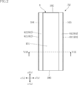
- FIG. 3 is a cross-sectional view taken along the line VIII-VIII of FIG.
- FIG. 6 is a cross-sectional view taken along the line XX-XX of FIG. It is a top view which shows the 1st conductor layer which concerns on 2nd Embodiment. It is a top view which shows the dielectric layer which concerns on 2nd Embodiment. It is a top view which shows the 2nd conductor layer which concerns on 2nd Embodiment. It is a top view which shows the insulating layer which concerns on 2nd Embodiment.
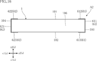
- the laminated capacitor A1 includes a laminated body 1 and a pair of external electrodes 61 and 62.
- the laminate 1 includes a plurality of first conductor layers 2, a plurality of second conductor layers 3, a plurality of dielectric layers 4, and a plurality of insulating layers 5.
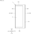
- FIG. 1 is a perspective view showing a multilayer capacitor A1.
- FIG. 2 is a plan view showing the multilayer capacitor A1.
- FIG. 3 is a bottom view showing the multilayer capacitor A1.
- FIG. 4 is a front view showing the multilayer capacitor A1.
- FIG. 5 is a rear view showing the multilayer capacitor A1.
- FIG. 6 is a left side view showing the multilayer capacitor A1.
- FIG. 7 is a right side view showing the multilayer capacitor A1.
- FIG. 8 is a cross-sectional view taken along the line VIII-VIII of FIG.
- FIG. 9 is a plan view showing each first conductor layer 2.
- FIG. 10 is a plan view showing each dielectric layer 4.
- FIG. 11 is a plan view showing each second conductor layer 3.
- FIG. 12 is a plan view showing each insulating layer 5.
- the three directions orthogonal to each other are the x direction, the y direction, and the z direction.
- the z direction is the thickness direction of the multilayer capacitor A1.
- the x direction is the left-right direction in the plan view (see FIG. 2) of the multilayer capacitor A1.
- the y direction is the vertical direction in the plan view (see FIG. 2) of the multilayer capacitor A1.
- One in the x direction is the x1 direction, and the other in the x direction is the x2 direction.
- one in the y direction is the y1 direction
- the other in the y direction is the y2 direction
- one in the z direction is the z1 direction
- the other in the z direction is the z2 direction.
- "planar view” means when viewed in the z direction.
- the z direction is an example of the "first direction”
- the x direction is an example of the "second direction”
- the y direction is an example of the "third direction”.
- the laminated body 1 is, for example, a substantially rectangular parallelepiped. As shown in FIG. 2, the laminated body 1 has a rectangular shape in a plan view in which the x direction is the lateral direction and the y direction is the longitudinal direction.
- the laminated body 1 has a main surface 101, a back surface 102, and a plurality of side surfaces 103 to 106.
- the main surface 101 and the back surface 102 are separated in the z direction as shown in FIGS. 4 to 8.
- the main surface 101 faces the z2 direction, and the back surface 102 faces the z1 direction.
- the plurality of side surfaces 103 to 106 are located between the main surface 101 and the back surface 102 in the z direction, and are connected to the main surface 101 and the back surface 102, respectively.
- the side surface 103 and the side surface 104 are separated in the x direction as shown in FIGS. 2 and 3.
- the side surface 103 faces the x2 direction, and the side surface 104 faces the x1 direction.
- the side surfaces 105 and 106 are separated in the y direction, as shown in FIGS. 2 and 3.
- the side surface 105 faces the y2 direction, and the side surface 106 faces the y1 direction.
- the side surface 103 is an example of the "first side surface”
- the side surface 104 is an example of the "second side surface”.
- the laminate 1 includes a plurality of first conductor layers 2, a plurality of second conductor layers 3, a plurality of dielectric layers 4, and a plurality of insulating layers 5.
- the laminate 1 has three first conductor layers 2a to 2c, three second conductor layers 3a to 3c, three dielectric layers 4a to 4c, and four insulations. It contains layers 5a-5d.
- the plurality of first conductor layers 2, the plurality of second conductor layers 3, the plurality of dielectric layers 4, and the plurality of insulating layers 5 are laminated in the z direction according to the configuration described in detail later.
- a combination of the plurality of first conductor layers 2 and the plurality of second conductor layers 3 is an example of the "plurality of conductor layers".
- Each of the plurality of first conductor layers 2 is made of, for example, Cu.
- the thickness of each first conductor layer 2 is, for example, 30 ⁇ m or more and 70 ⁇ m or less.
- each first conductor layer 2 has an edge on the x2 direction side exposed from the side surface 103.
- the plurality of first conductor layers 2 overlap each other in a plan view.
- each first conductor layer 2 extends from the edge of the laminated body 1 on the x2 direction side toward the x1 direction in a plan view.
- each first conductor layer 2 has an edge on the x2 direction side exposed from the side surface 103 and an edge on the x1 direction side not exposed from the side surface 104.
- each first conductor layer 2 on the x1 direction side is located inside the laminated body 1 with respect to the side surface 104. Further, as shown in FIG. 9, each first conductor layer 2 is not exposed from either the side surface 105 or the side surface 106 in a plan view. Therefore, in a plan view, the edge of each first conductor layer 2 on the y1 direction side is located inside the laminated body 1 with respect to the side surface 106, and the edge on the y2 direction side is the laminated body with respect to the side surface 105. It is located inside 1.
- an insulator 29 is formed around each first conductor layer 2 (excluding the edge on the x2 direction side). Specifically, the insulator 29 is provided between the first conductor layer 2 and the side surface 104, between the first conductor layer 2 and the side surface 105, and between the first conductor layer 2 and the side surface 106. Located in. The insulator 29 is made of the same material as the insulating layer 5 described later.
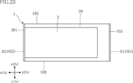
- Each of the plurality of second conductor layers 3 is made of, for example, Cu.
- the thickness of each second conductor layer 3 is, for example, 30 ⁇ m or more and 70 ⁇ m or less.
- each second conductor layer 3 has an edge on the x1 direction side exposed from the side surface 104.
- the plurality of second conductor layers 3 overlap each other in a plan view.
- each second conductor layer 3 extends from the edge of the laminated body 1 on the x1 direction side toward the x2 direction in a plan view.
- each second conductor layer 3 has an edge on the x1 direction side exposed from the side surface 104 and an edge on the x2 direction side not exposed from the side surface 103.
- each second conductor layer 3 on the x2 direction side is located inside the laminated body 1 with respect to the side surface 103. Further, as shown in FIG. 11, each second conductor layer 3 is not exposed from either the side surface 105 or the side surface 106 in a plan view. Therefore, in a plan view, the edge of each second conductor layer 3 on the y1 direction side is located inside the laminated body 1 with respect to the side surface 106, and the edge on the y2 direction side is the laminated body with respect to the side surface 105. It is located inside 1.
- an insulator 39 is formed around each second conductor layer 3 (excluding the edge on the x1 direction side). Specifically, the insulator 39 is provided between the second conductor layer 3 and the side surface 103, between the second conductor layer 3 and the side surface 105, and between the second conductor layer 3 and the side surface 106. Located in. The insulator 39 is made of the same material as the insulator 29. That is, the insulator 39 is the same material as the insulating layer 5 described later.
- the plurality of first conductor layers 2 and the plurality of second conductor layers 3 partially overlap in a plan view. Further, the plurality of first conductor layers 2 and the plurality of second conductor layers 3 have opposite polarities to each other when the laminated capacitor A1 is energized.
- each dielectric layer 4 is sandwiched between each first conductor layer 2 and each second conductor layer 3.
- the dielectric layer 4a is sandwiched between the first conductor layer 2a and the second conductor layer 3a.
- the dielectric layer 4b is sandwiched between the second conductor layer 3b and the first conductor layer 2b.
- the dielectric layer 4c is sandwiched between the first conductor layer 2c and the second conductor layer 3c.
- each dielectric layer 4 is connected from the edge of the laminate 1 on the x1 direction side to the edge on the x2 direction side of the laminate 1 in a plan view, and is on the y1 direction side of the laminate 1. It is connected from the edge to the edge on the y2 direction side.
- Each dielectric layer 4 is made of a film-like resin material such as a polymer film.
- the constituent material of each dielectric layer 4 is not limited to the film-shaped resin material, and may be any material having a relative permittivity of more than 1, for example. Examples of such a material include ceramics containing a metal oxide perovskite compound as a main component.
- the thickness of each dielectric layer 4 is, for example, 8 ⁇ m or more and 25 ⁇ m or less.
- Each of the plurality of insulating layers 5 is made of, for example, a prepreg.
- Each insulating layer 5 insulates two first conductor layers 2 and two second conductor layers 3 in contact with each of both surfaces in the z direction.
- Each insulating layer 5 has a lower dielectric strength than each dielectric layer 4.
- each insulating layer 5 also functions as an adhesive layer of two first conductor layers 2 and two second conductor layers 3 in contact with each of both sides in the z direction.
- the thickness of each insulating layer 5 is, for example, 40 ⁇ m or more and 100 ⁇ m or less.
- the plurality of insulating layers 5 are sandwiched between two first conductor layers 2 between two dielectric layers 4 adjacent to each other in the z direction, and two adjacent layers 5 in the z direction. Among the dielectric layers 4, the one sandwiched between the two second conductor layers 3 is included. Further, as shown in FIG. 8, the plurality of insulating layers 5 are a pair of external electrodes 61 and 62 (main surface covering portions 612 and 622 described later) and a first conductor layer formed on the main surface 101 of the laminated body 1.
- the insulating layer 5a is the surface layer of the laminated body 1 on the z2 direction side, and is sandwiched between the main surface covering portions 612 and 622 and the first conductor layer 2a, which will be described later.
- the insulating layer 5b is sandwiched between the second conductor layer 3a and the second conductor layer 3b between the two dielectric layers 4a and 4b.
- the insulating layer 5c is sandwiched between the first conductor layer 2b and the first conductor layer 2c between the two dielectric layers 4b and 4c.
- the insulating layer 5d is a surface layer of the laminate 1 on the z1 direction side, and is sandwiched between the back surface covering portions 613 and 623 and the second conductor layer 3c, which will be described later.
- the laminated body 1 includes a first unit in which the first conductor layer 2, the dielectric layer 4, and the second conductor layer 3 are laminated in this order in the z direction, and the second conductor layer 3 from the z2 direction to the z1 direction.
- the second unit in which the dielectric layer 4 and the first conductor layer 2 are laminated in this order are alternately overlapped with the insulating layer 5 interposed therebetween.
- the number of each of the first unit and the second unit is not particularly limited, and the numbers of the first unit and the second unit do not have to be the same. In the example shown in FIG. 8, the insulating layer 5, the first unit, the insulating layer 5, the second unit, the insulating layer 5, the first unit, and the insulating layer 5 are superposed in this order.
- each surface layer on both sides in the z direction may be configured to be a dielectric layer 4.
- the x-direction dimension, the y-direction dimension and the z-direction dimension (thickness) of each layer each first conductor layer 2, each second conductor layer 3, dielectric layer 4, and insulating layer 5
- the constituent materials of the above, the number of layers of each layer, and the like are not particularly limited, and can be appropriately changed based on the specifications (for example, capacitance, size, etc.) of the multilayer capacitor A1.
- ⁇ 0 is the dielectric constant of the vacuum
- ⁇ r is the relative permittivity of the dielectric (each dielectric layer 4)
- S is the internal electrode (each first conductor layer 2 and each second conductor layer 3 in plan view.
- d represents the distance between the electrodes (between each first conductor layer 2 and each second conductor layer 3)
- N represents the number of layers of the dielectric layer 4.
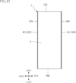
- the pair of external electrodes 61 and 62 are formed so as to cover a part of the main surface 101, a part of the back surface 102, and the side surfaces 103 and 104 of the laminated body 1.
- the pair of external electrodes 61 and 62 are terminals of the multilayer capacitor A1.
- the pair of external electrodes 61 and 62 are separated from each other and insulated from each other.
- the pair of external electrodes 61, 62 is made of, for example, Cu, but is not limited thereto.
- the pair of external electrodes 61, 62 is formed by, for example, plating, but is not limited thereto.
- the external electrode 61 is one terminal of the multilayer capacitor A1.
- the external electrode 61 includes a side covering portion 611, a main surface covering portion 612, and a back surface covering portion 613.
- the side surface covering portion 611 covers the side surface 103 as shown in FIGS. 1 to 5, 7 and 8.
- the main surface covering portion 612 covers a part of the main surface 101 as shown in FIGS. 1, 2, 4, 5, and 8. As shown in FIG. 2, the main surface covering portion 612 is formed on the portion of the main surface 101 on the x2 direction side.
- the main surface covering portion 612 is connected to the side covering portion 611.
- the back surface covering portion 613 covers a part of the back surface 102 as shown in FIGS. 3 to 5 and 8. As shown in FIG.
- the back surface covering portion 613 is formed on the back surface 102 on the x2 direction side.
- the back surface covering portion 613 is connected to the side surface covering portion 611.
- the main surface covering portion 612 and the back surface covering portion 613 do not overlap each of the second conductor layers 3 in a plan view.
- the external electrode 61 may further include a portion that is connected to the side surface covering portion 611, the main surface covering portion 612, and the back surface covering portion 613 and that partially covers the two side surfaces 105 and 106. Further, the external electrode 61 may not include the main surface covering portion 612 and the back surface covering portion 613.
- each insulator 39 is arranged between the side surface 103 and each of the second conductor layers 3, as shown in FIG. 11, the side surface covering portion 611 and each of the second conductor layers 3 are arranged in the x direction. Each insulator 39 is arranged between and. Therefore, each insulator 39 insulates the side surface covering portion 611 and each second conductor layer 3. Further, as shown in FIGS. 8 and 9, since the side surface covering portion 611 is in contact with the edge of each first conductor layer 2 on the x2 direction side, the side surface covering portion 611 is separated in the z direction. A plurality of arranged first conductor layers 2 are electrically connected. Therefore, the plurality of first conductor layers 2 have the same potential with each other via the side surface covering portion 611.
- the side surface covering portion 611 is an example of the “first side surface electrode”.
- the external electrode 62 is the other terminal of the multilayer capacitor A1.
- the external electrode 62 includes a side surface covering portion 621, a main surface covering portion 622, and a back surface covering portion 623.
- the side covering portion 621 covers the side surface 104 as shown in FIGS. 2 to 6 and 8.
- the main surface covering portion 622 covers a part of the main surface 101 as shown in FIGS. 2, 4, 5, and 8.
- the main surface covering portion 622 is formed on the portion of the main surface 101 on the x1 direction side, and is separated from the main surface covering portion 612 (external electrode 61).
- the main surface covering portion 622 is connected to the side covering portion 621.
- the back surface covering portion 623 covers a part of the back surface 102 as shown in FIGS.
- the back surface covering portion 623 is formed on the portion of the back surface 102 on the x1 direction side, and is separated from the back surface covering portion 613 (external electrode 61).
- the back surface covering portion 623 is connected to the side surface covering portion 621.
- the main surface covering portion 622 and the back surface covering portion 623 do not overlap each of the first conductor layers 2 in a plan view.
- the external electrode 62 may further include a portion connected to the side surface covering portion 621, the main surface covering portion 622, and the back surface covering portion 623, and further covering a part of the two side surfaces 105 and 106. Further, the external electrode 62 does not have to include the main surface covering portion 622 and the back surface covering portion 623.
- each insulator 29 is arranged between the side surface 104 and each of the first conductor layers 2, as shown in FIG. 9, the side surface covering portion 621 and each of the first conductor layers 2 are arranged in the x direction. Each insulator 29 is arranged between and. Therefore, each insulator 29 insulates the side surface covering portion 621 and each first conductor layer 2. Further, as shown in FIGS. 8 and 11, since the side surface covering portion 621 is in contact with the edge of each second conductor layer 3 on the x1 direction side, the side surface covering portion 621 is separated in the z direction. A plurality of arranged second conductor layers 3 are electrically connected. Therefore, the plurality of second conductor layers 3 have the same potential with each other via the side surface covering portion 621.
- the side surface covering portion 621 is an example of the “second side surface electrode”.
- the plurality of dielectric layers 4 are sandwiched between the first conductor layer 2 and the second conductor layer 3 in the z direction, respectively.
- the plurality of insulating layers 5 include two first conductor layers 2 (for example, first conductor layers 2b and 2c) between two dielectric layers 4 (for example, dielectric layers 4b and 4c) adjacent to each other in the z direction. It is sandwiched between two second conductor layers 3 (for example, second conductor layers 3a and 3b) between two dielectric layers 4 (for example, dielectric layers 4a and 4b) adjacent to each other in the z direction. There is something that has been done.
- Each insulating layer 5 has a lower dielectric strength than each dielectric layer 4.
- the dielectric layer 4 is sandwiched between two conductor layers (first conductor layer 2 and second conductor layer 3) having different potentials, and the insulating layer 5 is two conductor layers (two conductor layers) having the same potential.
- the structure is sandwiched between the first conductor layer 2 or two second conductor layers 3). Therefore, when a potential difference occurs between the plurality of first conductor layers 2 and the plurality of second conductor layers 3 when the multilayer capacitor A1 is energized, a voltage is applied to the thickness direction (z direction) of the dielectric layer 4. However, no voltage is applied in the thickness direction (z direction) of the insulating layer 5. Therefore, it is not necessary to guarantee the withstand voltage (dielectric strength) of the insulating layer 5. That is, the multilayer capacitor A1 can suppress a decrease in the dielectric strength.
- the dielectric layer 4 is a resin material
- the insulating layer 5 is a prepreg.
- Conventional multilayer capacitors include ceramic capacitors in which the dielectric layer 4 is made of ceramic. Due to its physical properties, ceramics are easily cracked by stress such as thermal stress. Therefore, in the ceramic capacitor, the dielectric layer 4 may be cracked or otherwise broken due to the heat generated when the ceramic capacitor is energized. Due to this destruction, the dielectric strength of the dielectric layer 4 is lowered.
- the multilayer capacitor A1 of the present disclosure since the dielectric layer 4 is not ceramic, the occurrence of cracks due to thermal stress can be suppressed. Therefore, the multilayer capacitor A1 can suppress a decrease in the dielectric strength.
- each of the first conductor layers 2 is covered with an insulator 29 at the edge on the y1 direction side and the edge on the y2 direction side, respectively. Further, in each of the second conductor layers 3, the edge on the y1 direction side and the edge on the y2 direction side are each covered with an insulator 39. According to this configuration, the first conductor layer 2 and the second conductor layer 3 are not exposed on the side surfaces 105 and 106 of the laminated body 1, respectively. Therefore, it is possible to prevent an unintended short circuit between the first conductor layer 2 and the second conductor layer 3 on the side surfaces 105 and 106.
- ⁇ Second Embodiment> 13 to 24 show the multilayer capacitor A2 according to the second embodiment.
- FIG. 13 is a perspective view showing the multilayer capacitor A2.
- FIG. 14 is a plan view showing the multilayer capacitor A2.
- FIG. 15 is a bottom view showing the multilayer capacitor A2.
- FIG. 16 is a front view showing the multilayer capacitor A2.
- FIG. 17 is a rear view showing the multilayer capacitor A2.
- FIG. 18 is a left side view showing the multilayer capacitor A2.
- FIG. 19 is a right side view showing the multilayer capacitor A2.
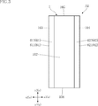
- FIG. 20 is a cross-sectional view taken along the line XX-XX of FIG.
- FIG. 21 is a plan view showing each of the first conductor layers 2 according to the second embodiment.
- FIG. 22 is a plan view showing each dielectric layer 4 according to the second embodiment.
- FIG. 23 is a plan view showing each of the second conductor layers 3 according to the second embodiment.
- FIG. 24 is a plan view showing each insulating layer 5 according to the second embodiment.
- the multilayer capacitor A2 is a substantially rectangular parallelepiped like the multilayer capacitor A1.
- the laminated capacitor A2 has a rectangular shape in the longitudinal direction in the x direction and the lateral direction in the y direction in a plan view.
- the laminate 1 (a plurality of first conductor layers 2, a plurality of second conductor layers 3, a plurality of dielectric layers 4 and a plurality of insulating layers 5), which are components of the multilayer capacitor A2, and the plurality of insulating layers 5
- the pair of external electrodes 61 and 62 are configured in the same manner as the multilayer capacitor A1.
- the plurality of dielectric layers 4 are sandwiched between the first conductor layer 2 and the second conductor layer in the z direction, respectively.
- the plurality of insulating layers 5 are sandwiched between two first conductor layers 2 (for example, first conductor layers 2b and 2c) and two second conductor layers 3 (for example, second conductor layers 3a and 3b). Some are sandwiched.
- the multilayer capacitor A2 can suppress a decrease in the dielectric strength.
- the multilayer capacitor A2 can exhibit the same effect as the above-mentioned multilayer capacitor A1.
- the multilayer capacitor according to the present disclosure is not limited to the above-described embodiment.
- the specific configuration of each part of the multilayer capacitor of the present disclosure can be freely redesigned.
Abstract
La présente invention concerne un condensateur multicouche comprenant un stratifié ayant une première surface latérale et une seconde surface latérale, une première partie de revêtement de surface latérale recouvrant la première surface latérale, et une seconde partie de revêtement de surface latérale recouvrant la seconde surface latérale. Le stratifié est obtenu par stratification, dans la direction z, d'une pluralité de premières couches conductrices, d'une pluralité de secondes couches conductrices, d'une pluralité de couches diélectriques et d'une pluralité de couches isolantes. Chaque couche de la pluralité de premières couches conductrices est reliée à la première partie de revêtement de surface latérale et espacée de la seconde partie de revêtement de surface latérale. Chaque couche de la pluralité de secondes couches conductrices est reliée à la seconde partie de revêtement de surface latérale et espacée de la première partie de revêtement de surface latérale. La pluralité de couches isolantes ont une résistance diélectrique inférieure à celle de la pluralité de couches diélectriques. Chaque couche de la pluralité de couches diélectriques est prise en sandwich par une première couche conductrice et une seconde couche conductrice 3. La pluralité de couches isolantes comprennent une couche isolante prise en sandwich par deux premières couches conductrices 2 et une couche isolante prise en sandwich par deux secondes couches conductrices 3.
Priority Applications (4)
| Application Number | Priority Date | Filing Date | Title |
|---|---|---|---|
| US17/905,385 US20230129081A1 (en) | 2020-03-19 | 2021-03-03 | Multilayer capacitor |
| CN202180022139.4A CN115335933A (zh) | 2020-03-19 | 2021-03-03 | 层叠型电容器 |
| DE112021001060.3T DE112021001060T5 (de) | 2020-03-19 | 2021-03-03 | Mehrschichtkondensator |
| JP2022508197A JPWO2021187113A1 (fr) | 2020-03-19 | 2021-03-03 |
Applications Claiming Priority (2)
| Application Number | Priority Date | Filing Date | Title |
|---|---|---|---|
| JP2020-048991 | 2020-03-19 | ||
| JP2020048991 | 2020-03-19 |
Publications (1)
| Publication Number | Publication Date |
|---|---|
| WO2021187113A1 true WO2021187113A1 (fr) | 2021-09-23 |
Family
ID=77768109
Family Applications (1)
| Application Number | Title | Priority Date | Filing Date |
|---|---|---|---|
| PCT/JP2021/008204 WO2021187113A1 (fr) | 2020-03-19 | 2021-03-03 | Condensateur multicouche |
Country Status (5)
| Country | Link |
|---|---|
| US (1) | US20230129081A1 (fr) |
| JP (1) | JPWO2021187113A1 (fr) |
| CN (1) | CN115335933A (fr) |
| DE (1) | DE112021001060T5 (fr) |
| WO (1) | WO2021187113A1 (fr) |
Citations (5)
| Publication number | Priority date | Publication date | Assignee | Title |
|---|---|---|---|---|
| JPS59127829A (ja) * | 1983-01-12 | 1984-07-23 | 松下電器産業株式会社 | チツプ状フイルムコンデンサ− |
| JPH0273614A (ja) * | 1988-09-08 | 1990-03-13 | Murata Mfg Co Ltd | 積層コンデンサ |
| JP2011135038A (ja) * | 2009-12-22 | 2011-07-07 | Samsung Electro-Mechanics Co Ltd | 積層セラミックキャパシタ |
| WO2012157300A1 (fr) * | 2011-05-19 | 2012-11-22 | 株式会社村田製作所 | Composant électronique en céramique stratifiée composite |
| JP2018182321A (ja) * | 2017-04-10 | 2018-11-15 | プレシディオ・コンポーネンツ・インコーポレイテッド | 内部エアギャップキャパシタンスを備える多層広帯域セラミックキャパシタ |
Family Cites Families (3)
| Publication number | Priority date | Publication date | Assignee | Title |
|---|---|---|---|---|
| JP3470830B2 (ja) | 1994-09-26 | 2003-11-25 | 株式会社村田製作所 | 積層コンデンサの製造方法 |
| JP2007042743A (ja) * | 2005-08-01 | 2007-02-15 | Tdk Corp | 積層電子部品 |
| KR102163418B1 (ko) * | 2018-11-02 | 2020-10-08 | 삼성전기주식회사 | 적층 세라믹 커패시터 |
-
2021
- 2021-03-03 US US17/905,385 patent/US20230129081A1/en active Pending
- 2021-03-03 DE DE112021001060.3T patent/DE112021001060T5/de active Pending
- 2021-03-03 CN CN202180022139.4A patent/CN115335933A/zh active Pending
- 2021-03-03 WO PCT/JP2021/008204 patent/WO2021187113A1/fr active Application Filing
- 2021-03-03 JP JP2022508197A patent/JPWO2021187113A1/ja active Pending
Patent Citations (5)
| Publication number | Priority date | Publication date | Assignee | Title |
|---|---|---|---|---|
| JPS59127829A (ja) * | 1983-01-12 | 1984-07-23 | 松下電器産業株式会社 | チツプ状フイルムコンデンサ− |
| JPH0273614A (ja) * | 1988-09-08 | 1990-03-13 | Murata Mfg Co Ltd | 積層コンデンサ |
| JP2011135038A (ja) * | 2009-12-22 | 2011-07-07 | Samsung Electro-Mechanics Co Ltd | 積層セラミックキャパシタ |
| WO2012157300A1 (fr) * | 2011-05-19 | 2012-11-22 | 株式会社村田製作所 | Composant électronique en céramique stratifiée composite |
| JP2018182321A (ja) * | 2017-04-10 | 2018-11-15 | プレシディオ・コンポーネンツ・インコーポレイテッド | 内部エアギャップキャパシタンスを備える多層広帯域セラミックキャパシタ |
Also Published As
| Publication number | Publication date |
|---|---|
| US20230129081A1 (en) | 2023-04-27 |
| CN115335933A (zh) | 2022-11-11 |
| DE112021001060T5 (de) | 2022-12-01 |
| JPWO2021187113A1 (fr) | 2021-09-23 |
Similar Documents
| Publication | Publication Date | Title |
|---|---|---|
| JP4450084B2 (ja) | 積層コンデンサ及び積層コンデンサの実装構造 | |
| US8526162B2 (en) | Feedthrough multilayer capacitor | |
| US7411775B2 (en) | Feedthrough multilayer capacitor array | |
| CN108364785B (zh) | 层叠电容器及电子部件装置 | |
| KR20190116173A (ko) | 적층형 전자 부품 | |
| TWI399770B (zh) | Laminated capacitors | |
| KR20190064938A (ko) | 적층형 커패시터 | |
| US8068330B2 (en) | Multilayer capacitor | |
| JP4475338B2 (ja) | 積層コンデンサ | |
| JP5170066B2 (ja) | 積層コンデンサ | |
| JP4483904B2 (ja) | 貫通型積層コンデンサ | |
| JP4428446B2 (ja) | 積層コンデンサ | |
| JPH0955335A (ja) | 積層型貫通コンデンサ | |
| WO2021187113A1 (fr) | Condensateur multicouche | |
| KR20180026932A (ko) | 커패시터 부품 | |
| US8107216B2 (en) | Multilayer capacitor | |
| JP2021015962A (ja) | 積層型キャパシタ及びその実装基板 | |
| JP5131263B2 (ja) | 積層コンデンサ | |
| KR100916480B1 (ko) | 적층 세라믹 캐패시터 | |
| JP4412386B2 (ja) | 貫通型積層コンデンサ | |
| JP7003496B2 (ja) | 電子部品装置 | |
| JP6930114B2 (ja) | 電子部品装置 | |
| JP2024051994A (ja) | 電子部品 | |
| JP5170065B2 (ja) | 積層コンデンサ | |
| KR20190121231A (ko) | 적층형 커패시터 |
Legal Events
| Date | Code | Title | Description |
|---|---|---|---|
| 121 | Ep: the epo has been informed by wipo that ep was designated in this application |
Ref document number: 21772126 Country of ref document: EP Kind code of ref document: A1 |
|
| ENP | Entry into the national phase |
Ref document number: 2022508197 Country of ref document: JP Kind code of ref document: A |
|
| 122 | Ep: pct application non-entry in european phase |
Ref document number: 21772126 Country of ref document: EP Kind code of ref document: A1 |