WO2021187113A1 - Multilayer capacitor - Google Patents
Multilayer capacitor Download PDFInfo
- Publication number
- WO2021187113A1 WO2021187113A1 PCT/JP2021/008204 JP2021008204W WO2021187113A1 WO 2021187113 A1 WO2021187113 A1 WO 2021187113A1 JP 2021008204 W JP2021008204 W JP 2021008204W WO 2021187113 A1 WO2021187113 A1 WO 2021187113A1
- Authority
- WO
- WIPO (PCT)
- Prior art keywords
- layers
- conductor
- layer
- dielectric
- conductor layers
- Prior art date
Links
- 239000003990 capacitor Substances 0.000 title claims abstract description 83
- 239000004020 conductor Substances 0.000 claims abstract description 164
- 239000012212 insulator Substances 0.000 claims description 21
- 239000000463 material Substances 0.000 claims description 18
- 238000009413 insulation Methods 0.000 abstract description 7
- 238000010030 laminating Methods 0.000 abstract 1
- 239000010410 layer Substances 0.000 description 253
- 239000000919 ceramic Substances 0.000 description 4
- 239000011347 resin Substances 0.000 description 4
- 229920005989 resin Polymers 0.000 description 4
- 239000003985 ceramic capacitor Substances 0.000 description 3
- 239000002344 surface layer Substances 0.000 description 3
- 238000000576 coating method Methods 0.000 description 2
- 239000000470 constituent Substances 0.000 description 2
- 230000000694 effects Effects 0.000 description 2
- 229920006254 polymer film Polymers 0.000 description 2
- 230000008646 thermal stress Effects 0.000 description 2
- CHDVXKLFZBWKEN-UHFFFAOYSA-N C=C.F.F.F.Cl Chemical compound C=C.F.F.F.Cl CHDVXKLFZBWKEN-UHFFFAOYSA-N 0.000 description 1
- 239000012790 adhesive layer Substances 0.000 description 1
- 238000006243 chemical reaction Methods 0.000 description 1
- 239000011248 coating agent Substances 0.000 description 1
- 150000001875 compounds Chemical class 0.000 description 1
- 230000006378 damage Effects 0.000 description 1
- 238000009499 grossing Methods 0.000 description 1
- 239000011810 insulating material Substances 0.000 description 1
- 239000002184 metal Substances 0.000 description 1
- 229910044991 metal oxide Inorganic materials 0.000 description 1
- 150000004706 metal oxides Chemical class 0.000 description 1
- 230000000704 physical effect Effects 0.000 description 1
- 238000007747 plating Methods 0.000 description 1
- 238000000926 separation method Methods 0.000 description 1
- 230000035882 stress Effects 0.000 description 1
Images


Classifications
-
- H—ELECTRICITY
- H01—ELECTRIC ELEMENTS
- H01G—CAPACITORS; CAPACITORS, RECTIFIERS, DETECTORS, SWITCHING DEVICES OR LIGHT-SENSITIVE DEVICES, OF THE ELECTROLYTIC TYPE
- H01G4/00—Fixed capacitors; Processes of their manufacture
- H01G4/30—Stacked capacitors
-
- H—ELECTRICITY
- H01—ELECTRIC ELEMENTS
- H01G—CAPACITORS; CAPACITORS, RECTIFIERS, DETECTORS, SWITCHING DEVICES OR LIGHT-SENSITIVE DEVICES, OF THE ELECTROLYTIC TYPE
- H01G2/00—Details of capacitors not covered by a single one of groups H01G4/00-H01G11/00
- H01G2/02—Mountings
- H01G2/06—Mountings specially adapted for mounting on a printed-circuit support
-
- H—ELECTRICITY
- H01—ELECTRIC ELEMENTS
- H01G—CAPACITORS; CAPACITORS, RECTIFIERS, DETECTORS, SWITCHING DEVICES OR LIGHT-SENSITIVE DEVICES, OF THE ELECTROLYTIC TYPE
- H01G4/00—Fixed capacitors; Processes of their manufacture
- H01G4/002—Details
- H01G4/228—Terminals
- H01G4/232—Terminals electrically connecting two or more layers of a stacked or rolled capacitor
-
- H—ELECTRICITY
- H01—ELECTRIC ELEMENTS
- H01G—CAPACITORS; CAPACITORS, RECTIFIERS, DETECTORS, SWITCHING DEVICES OR LIGHT-SENSITIVE DEVICES, OF THE ELECTROLYTIC TYPE
- H01G4/00—Fixed capacitors; Processes of their manufacture
- H01G4/38—Multiple capacitors, i.e. structural combinations of fixed capacitors
- H01G4/385—Single unit multiple capacitors, e.g. dual capacitor in one coil
-
- H—ELECTRICITY
- H01—ELECTRIC ELEMENTS
- H01G—CAPACITORS; CAPACITORS, RECTIFIERS, DETECTORS, SWITCHING DEVICES OR LIGHT-SENSITIVE DEVICES, OF THE ELECTROLYTIC TYPE
- H01G4/00—Fixed capacitors; Processes of their manufacture
- H01G4/002—Details
- H01G4/005—Electrodes
- H01G4/012—Form of non-self-supporting electrodes
-
- H—ELECTRICITY
- H01—ELECTRIC ELEMENTS
- H01G—CAPACITORS; CAPACITORS, RECTIFIERS, DETECTORS, SWITCHING DEVICES OR LIGHT-SENSITIVE DEVICES, OF THE ELECTROLYTIC TYPE
- H01G4/00—Fixed capacitors; Processes of their manufacture
- H01G4/002—Details
- H01G4/228—Terminals
- H01G4/232—Terminals electrically connecting two or more layers of a stacked or rolled capacitor
- H01G4/2325—Terminals electrically connecting two or more layers of a stacked or rolled capacitor characterised by the material of the terminals
-
- H—ELECTRICITY
- H01—ELECTRIC ELEMENTS
- H01G—CAPACITORS; CAPACITORS, RECTIFIERS, DETECTORS, SWITCHING DEVICES OR LIGHT-SENSITIVE DEVICES, OF THE ELECTROLYTIC TYPE
- H01G4/00—Fixed capacitors; Processes of their manufacture
- H01G4/30—Stacked capacitors
- H01G4/304—Stacked capacitors obtained from a another capacitor
-
- H—ELECTRICITY
- H01—ELECTRIC ELEMENTS
- H01G—CAPACITORS; CAPACITORS, RECTIFIERS, DETECTORS, SWITCHING DEVICES OR LIGHT-SENSITIVE DEVICES, OF THE ELECTROLYTIC TYPE
- H01G4/00—Fixed capacitors; Processes of their manufacture
- H01G4/38—Multiple capacitors, i.e. structural combinations of fixed capacitors
Definitions
- This disclosure relates to multilayer capacitors.
- Patent Document 1 discloses a conventional multilayer capacitor.
- the multilayer capacitor described in Patent Document 1 includes a plurality of first internal electrodes, a plurality of second internal electrodes, a plurality of dielectric films, a plurality of insulating materials, and a pair of external electrodes.
- Each of the first internal electrodes and each of the second internal electrodes is a metal film.
- the plurality of first internal electrodes are connected by one of the pair of external electrodes, and the plurality of second internal electrodes are connected by the other of the pair of external electrodes.
- the plurality of first internal electrodes and the plurality of second internal electrodes have opposite polarities to each other when the multilayer capacitor is energized.
- Each insulating film is a plastic polymer film such as ethylene trifluoride chloride resin.
- each insulating film, each first internal electrode, each dielectric film, and each second internal electrode are laminated in this order, and a plurality of these laminated bodies are laminated. Therefore, each insulating film is sandwiched between each first internal electrode and each second internal electrode to insulate them.
- the dielectric strength of this laminated capacitor is limited to the lower of the dielectric strength of the dielectric layer and the dielectric strength of the insulating film. In particular, when the dielectric strength of the insulating film is lower than the dielectric strength of the dielectric layer, the dielectric strength of the multilayer capacitor is lowered.
- This disclosure was conceived in view of the above circumstances, and one of the problems is to provide a multilayer capacitor capable of suppressing a decrease in dielectric strength.
- the multilayer capacitor provided by the present disclosure has a main surface and a back surface that face each other in the first direction, and a first side surface and a back surface that face each other in the second direction orthogonal to the first direction. It includes a laminate having a second side surface, a first side surface electrode covering the first side surface, and a second side surface electrode covering the second side surface.
- a plurality of conductor layers, a plurality of dielectric layers, and a plurality of insulating layers are laminated in the first direction.
- the plurality of conductor layers include a plurality of first conductor layers and a plurality of second conductor layers separated from each other in the first direction, and each of the plurality of first conductor layers is connected to the first side electrode.
- Each of the plurality of second conductor layers is connected to the second side surface electrode and separated from the first side surface electrode.
- Each of the plurality of insulating layers has a lower dielectric strength than each of the plurality of dielectric layers.
- Each of the plurality of dielectric layers is sandwiched between each of the plurality of first conductor layers and each of the plurality of second conductor layers.
- the plurality of insulating layers include one sandwiched between the two first conductor layers between the two dielectric layers adjacent to the first direction and the two dielectric layers adjacent to the first direction. There is one sandwiched between the two second conductor layers between the body layers.
- each of the plurality of dielectric layers is in contact with both the first side electrode and the second side electrode.
- each of the plurality of dielectric layers is connected from one end edge to the other end edge of the laminate in the first direction and the third direction orthogonal to the second direction.
- an insulator made of the same material as the material of the plurality of insulating layers is arranged between each of the plurality of first conductor layers and the second side electrode.
- an insulator made of the same material as the material of the plurality of insulating layers is arranged between each of the plurality of second conductor layers and the first side electrode.
- the multilayer capacitor of the present disclosure it is possible to suppress a decrease in dielectric strength.
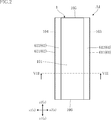
- FIG. 3 is a cross-sectional view taken along the line VIII-VIII of FIG.
- FIG. 6 is a cross-sectional view taken along the line XX-XX of FIG. It is a top view which shows the 1st conductor layer which concerns on 2nd Embodiment. It is a top view which shows the dielectric layer which concerns on 2nd Embodiment. It is a top view which shows the 2nd conductor layer which concerns on 2nd Embodiment. It is a top view which shows the insulating layer which concerns on 2nd Embodiment.
- the laminated capacitor A1 includes a laminated body 1 and a pair of external electrodes 61 and 62.
- the laminate 1 includes a plurality of first conductor layers 2, a plurality of second conductor layers 3, a plurality of dielectric layers 4, and a plurality of insulating layers 5.
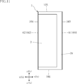
- FIG. 1 is a perspective view showing a multilayer capacitor A1.
- FIG. 2 is a plan view showing the multilayer capacitor A1.
- FIG. 3 is a bottom view showing the multilayer capacitor A1.
- FIG. 4 is a front view showing the multilayer capacitor A1.
- FIG. 5 is a rear view showing the multilayer capacitor A1.
- FIG. 6 is a left side view showing the multilayer capacitor A1.
- FIG. 7 is a right side view showing the multilayer capacitor A1.
- FIG. 8 is a cross-sectional view taken along the line VIII-VIII of FIG.
- FIG. 9 is a plan view showing each first conductor layer 2.
- FIG. 10 is a plan view showing each dielectric layer 4.
- FIG. 11 is a plan view showing each second conductor layer 3.
- FIG. 12 is a plan view showing each insulating layer 5.
- the three directions orthogonal to each other are the x direction, the y direction, and the z direction.
- the z direction is the thickness direction of the multilayer capacitor A1.
- the x direction is the left-right direction in the plan view (see FIG. 2) of the multilayer capacitor A1.
- the y direction is the vertical direction in the plan view (see FIG. 2) of the multilayer capacitor A1.
- One in the x direction is the x1 direction, and the other in the x direction is the x2 direction.
- one in the y direction is the y1 direction
- the other in the y direction is the y2 direction
- one in the z direction is the z1 direction
- the other in the z direction is the z2 direction.
- "planar view” means when viewed in the z direction.
- the z direction is an example of the "first direction”
- the x direction is an example of the "second direction”
- the y direction is an example of the "third direction”.
- the laminated body 1 is, for example, a substantially rectangular parallelepiped. As shown in FIG. 2, the laminated body 1 has a rectangular shape in a plan view in which the x direction is the lateral direction and the y direction is the longitudinal direction.
- the laminated body 1 has a main surface 101, a back surface 102, and a plurality of side surfaces 103 to 106.
- the main surface 101 and the back surface 102 are separated in the z direction as shown in FIGS. 4 to 8.
- the main surface 101 faces the z2 direction, and the back surface 102 faces the z1 direction.
- the plurality of side surfaces 103 to 106 are located between the main surface 101 and the back surface 102 in the z direction, and are connected to the main surface 101 and the back surface 102, respectively.
- the side surface 103 and the side surface 104 are separated in the x direction as shown in FIGS. 2 and 3.
- the side surface 103 faces the x2 direction, and the side surface 104 faces the x1 direction.
- the side surfaces 105 and 106 are separated in the y direction, as shown in FIGS. 2 and 3.
- the side surface 105 faces the y2 direction, and the side surface 106 faces the y1 direction.
- the side surface 103 is an example of the "first side surface”
- the side surface 104 is an example of the "second side surface”.
- the laminate 1 includes a plurality of first conductor layers 2, a plurality of second conductor layers 3, a plurality of dielectric layers 4, and a plurality of insulating layers 5.
- the laminate 1 has three first conductor layers 2a to 2c, three second conductor layers 3a to 3c, three dielectric layers 4a to 4c, and four insulations. It contains layers 5a-5d.
- the plurality of first conductor layers 2, the plurality of second conductor layers 3, the plurality of dielectric layers 4, and the plurality of insulating layers 5 are laminated in the z direction according to the configuration described in detail later.
- a combination of the plurality of first conductor layers 2 and the plurality of second conductor layers 3 is an example of the "plurality of conductor layers".
- Each of the plurality of first conductor layers 2 is made of, for example, Cu.
- the thickness of each first conductor layer 2 is, for example, 30 ⁇ m or more and 70 ⁇ m or less.
- each first conductor layer 2 has an edge on the x2 direction side exposed from the side surface 103.
- the plurality of first conductor layers 2 overlap each other in a plan view.
- each first conductor layer 2 extends from the edge of the laminated body 1 on the x2 direction side toward the x1 direction in a plan view.
- each first conductor layer 2 has an edge on the x2 direction side exposed from the side surface 103 and an edge on the x1 direction side not exposed from the side surface 104.
- each first conductor layer 2 on the x1 direction side is located inside the laminated body 1 with respect to the side surface 104. Further, as shown in FIG. 9, each first conductor layer 2 is not exposed from either the side surface 105 or the side surface 106 in a plan view. Therefore, in a plan view, the edge of each first conductor layer 2 on the y1 direction side is located inside the laminated body 1 with respect to the side surface 106, and the edge on the y2 direction side is the laminated body with respect to the side surface 105. It is located inside 1.
- an insulator 29 is formed around each first conductor layer 2 (excluding the edge on the x2 direction side). Specifically, the insulator 29 is provided between the first conductor layer 2 and the side surface 104, between the first conductor layer 2 and the side surface 105, and between the first conductor layer 2 and the side surface 106. Located in. The insulator 29 is made of the same material as the insulating layer 5 described later.
- Each of the plurality of second conductor layers 3 is made of, for example, Cu.
- the thickness of each second conductor layer 3 is, for example, 30 ⁇ m or more and 70 ⁇ m or less.
- each second conductor layer 3 has an edge on the x1 direction side exposed from the side surface 104.
- the plurality of second conductor layers 3 overlap each other in a plan view.
- each second conductor layer 3 extends from the edge of the laminated body 1 on the x1 direction side toward the x2 direction in a plan view.
- each second conductor layer 3 has an edge on the x1 direction side exposed from the side surface 104 and an edge on the x2 direction side not exposed from the side surface 103.
- each second conductor layer 3 on the x2 direction side is located inside the laminated body 1 with respect to the side surface 103. Further, as shown in FIG. 11, each second conductor layer 3 is not exposed from either the side surface 105 or the side surface 106 in a plan view. Therefore, in a plan view, the edge of each second conductor layer 3 on the y1 direction side is located inside the laminated body 1 with respect to the side surface 106, and the edge on the y2 direction side is the laminated body with respect to the side surface 105. It is located inside 1.
- an insulator 39 is formed around each second conductor layer 3 (excluding the edge on the x1 direction side). Specifically, the insulator 39 is provided between the second conductor layer 3 and the side surface 103, between the second conductor layer 3 and the side surface 105, and between the second conductor layer 3 and the side surface 106. Located in. The insulator 39 is made of the same material as the insulator 29. That is, the insulator 39 is the same material as the insulating layer 5 described later.
- the plurality of first conductor layers 2 and the plurality of second conductor layers 3 partially overlap in a plan view. Further, the plurality of first conductor layers 2 and the plurality of second conductor layers 3 have opposite polarities to each other when the laminated capacitor A1 is energized.
- each dielectric layer 4 is sandwiched between each first conductor layer 2 and each second conductor layer 3.
- the dielectric layer 4a is sandwiched between the first conductor layer 2a and the second conductor layer 3a.
- the dielectric layer 4b is sandwiched between the second conductor layer 3b and the first conductor layer 2b.
- the dielectric layer 4c is sandwiched between the first conductor layer 2c and the second conductor layer 3c.
- each dielectric layer 4 is connected from the edge of the laminate 1 on the x1 direction side to the edge on the x2 direction side of the laminate 1 in a plan view, and is on the y1 direction side of the laminate 1. It is connected from the edge to the edge on the y2 direction side.
- Each dielectric layer 4 is made of a film-like resin material such as a polymer film.
- the constituent material of each dielectric layer 4 is not limited to the film-shaped resin material, and may be any material having a relative permittivity of more than 1, for example. Examples of such a material include ceramics containing a metal oxide perovskite compound as a main component.
- the thickness of each dielectric layer 4 is, for example, 8 ⁇ m or more and 25 ⁇ m or less.
- Each of the plurality of insulating layers 5 is made of, for example, a prepreg.
- Each insulating layer 5 insulates two first conductor layers 2 and two second conductor layers 3 in contact with each of both surfaces in the z direction.
- Each insulating layer 5 has a lower dielectric strength than each dielectric layer 4.
- each insulating layer 5 also functions as an adhesive layer of two first conductor layers 2 and two second conductor layers 3 in contact with each of both sides in the z direction.
- the thickness of each insulating layer 5 is, for example, 40 ⁇ m or more and 100 ⁇ m or less.
- the plurality of insulating layers 5 are sandwiched between two first conductor layers 2 between two dielectric layers 4 adjacent to each other in the z direction, and two adjacent layers 5 in the z direction. Among the dielectric layers 4, the one sandwiched between the two second conductor layers 3 is included. Further, as shown in FIG. 8, the plurality of insulating layers 5 are a pair of external electrodes 61 and 62 (main surface covering portions 612 and 622 described later) and a first conductor layer formed on the main surface 101 of the laminated body 1.
- the insulating layer 5a is the surface layer of the laminated body 1 on the z2 direction side, and is sandwiched between the main surface covering portions 612 and 622 and the first conductor layer 2a, which will be described later.
- the insulating layer 5b is sandwiched between the second conductor layer 3a and the second conductor layer 3b between the two dielectric layers 4a and 4b.
- the insulating layer 5c is sandwiched between the first conductor layer 2b and the first conductor layer 2c between the two dielectric layers 4b and 4c.
- the insulating layer 5d is a surface layer of the laminate 1 on the z1 direction side, and is sandwiched between the back surface covering portions 613 and 623 and the second conductor layer 3c, which will be described later.
- the laminated body 1 includes a first unit in which the first conductor layer 2, the dielectric layer 4, and the second conductor layer 3 are laminated in this order in the z direction, and the second conductor layer 3 from the z2 direction to the z1 direction.
- the second unit in which the dielectric layer 4 and the first conductor layer 2 are laminated in this order are alternately overlapped with the insulating layer 5 interposed therebetween.
- the number of each of the first unit and the second unit is not particularly limited, and the numbers of the first unit and the second unit do not have to be the same. In the example shown in FIG. 8, the insulating layer 5, the first unit, the insulating layer 5, the second unit, the insulating layer 5, the first unit, and the insulating layer 5 are superposed in this order.
- each surface layer on both sides in the z direction may be configured to be a dielectric layer 4.
- the x-direction dimension, the y-direction dimension and the z-direction dimension (thickness) of each layer each first conductor layer 2, each second conductor layer 3, dielectric layer 4, and insulating layer 5
- the constituent materials of the above, the number of layers of each layer, and the like are not particularly limited, and can be appropriately changed based on the specifications (for example, capacitance, size, etc.) of the multilayer capacitor A1.
- ⁇ 0 is the dielectric constant of the vacuum
- ⁇ r is the relative permittivity of the dielectric (each dielectric layer 4)
- S is the internal electrode (each first conductor layer 2 and each second conductor layer 3 in plan view.
- d represents the distance between the electrodes (between each first conductor layer 2 and each second conductor layer 3)
- N represents the number of layers of the dielectric layer 4.
- the pair of external electrodes 61 and 62 are formed so as to cover a part of the main surface 101, a part of the back surface 102, and the side surfaces 103 and 104 of the laminated body 1.
- the pair of external electrodes 61 and 62 are terminals of the multilayer capacitor A1.
- the pair of external electrodes 61 and 62 are separated from each other and insulated from each other.
- the pair of external electrodes 61, 62 is made of, for example, Cu, but is not limited thereto.
- the pair of external electrodes 61, 62 is formed by, for example, plating, but is not limited thereto.
- the external electrode 61 is one terminal of the multilayer capacitor A1.
- the external electrode 61 includes a side covering portion 611, a main surface covering portion 612, and a back surface covering portion 613.
- the side surface covering portion 611 covers the side surface 103 as shown in FIGS. 1 to 5, 7 and 8.
- the main surface covering portion 612 covers a part of the main surface 101 as shown in FIGS. 1, 2, 4, 5, and 8. As shown in FIG. 2, the main surface covering portion 612 is formed on the portion of the main surface 101 on the x2 direction side.
- the main surface covering portion 612 is connected to the side covering portion 611.
- the back surface covering portion 613 covers a part of the back surface 102 as shown in FIGS. 3 to 5 and 8. As shown in FIG.
- the back surface covering portion 613 is formed on the back surface 102 on the x2 direction side.
- the back surface covering portion 613 is connected to the side surface covering portion 611.
- the main surface covering portion 612 and the back surface covering portion 613 do not overlap each of the second conductor layers 3 in a plan view.
- the external electrode 61 may further include a portion that is connected to the side surface covering portion 611, the main surface covering portion 612, and the back surface covering portion 613 and that partially covers the two side surfaces 105 and 106. Further, the external electrode 61 may not include the main surface covering portion 612 and the back surface covering portion 613.
- each insulator 39 is arranged between the side surface 103 and each of the second conductor layers 3, as shown in FIG. 11, the side surface covering portion 611 and each of the second conductor layers 3 are arranged in the x direction. Each insulator 39 is arranged between and. Therefore, each insulator 39 insulates the side surface covering portion 611 and each second conductor layer 3. Further, as shown in FIGS. 8 and 9, since the side surface covering portion 611 is in contact with the edge of each first conductor layer 2 on the x2 direction side, the side surface covering portion 611 is separated in the z direction. A plurality of arranged first conductor layers 2 are electrically connected. Therefore, the plurality of first conductor layers 2 have the same potential with each other via the side surface covering portion 611.
- the side surface covering portion 611 is an example of the “first side surface electrode”.
- the external electrode 62 is the other terminal of the multilayer capacitor A1.
- the external electrode 62 includes a side surface covering portion 621, a main surface covering portion 622, and a back surface covering portion 623.
- the side covering portion 621 covers the side surface 104 as shown in FIGS. 2 to 6 and 8.
- the main surface covering portion 622 covers a part of the main surface 101 as shown in FIGS. 2, 4, 5, and 8.
- the main surface covering portion 622 is formed on the portion of the main surface 101 on the x1 direction side, and is separated from the main surface covering portion 612 (external electrode 61).
- the main surface covering portion 622 is connected to the side covering portion 621.
- the back surface covering portion 623 covers a part of the back surface 102 as shown in FIGS.
- the back surface covering portion 623 is formed on the portion of the back surface 102 on the x1 direction side, and is separated from the back surface covering portion 613 (external electrode 61).
- the back surface covering portion 623 is connected to the side surface covering portion 621.
- the main surface covering portion 622 and the back surface covering portion 623 do not overlap each of the first conductor layers 2 in a plan view.
- the external electrode 62 may further include a portion connected to the side surface covering portion 621, the main surface covering portion 622, and the back surface covering portion 623, and further covering a part of the two side surfaces 105 and 106. Further, the external electrode 62 does not have to include the main surface covering portion 622 and the back surface covering portion 623.
- each insulator 29 is arranged between the side surface 104 and each of the first conductor layers 2, as shown in FIG. 9, the side surface covering portion 621 and each of the first conductor layers 2 are arranged in the x direction. Each insulator 29 is arranged between and. Therefore, each insulator 29 insulates the side surface covering portion 621 and each first conductor layer 2. Further, as shown in FIGS. 8 and 11, since the side surface covering portion 621 is in contact with the edge of each second conductor layer 3 on the x1 direction side, the side surface covering portion 621 is separated in the z direction. A plurality of arranged second conductor layers 3 are electrically connected. Therefore, the plurality of second conductor layers 3 have the same potential with each other via the side surface covering portion 621.
- the side surface covering portion 621 is an example of the “second side surface electrode”.
- the plurality of dielectric layers 4 are sandwiched between the first conductor layer 2 and the second conductor layer 3 in the z direction, respectively.
- the plurality of insulating layers 5 include two first conductor layers 2 (for example, first conductor layers 2b and 2c) between two dielectric layers 4 (for example, dielectric layers 4b and 4c) adjacent to each other in the z direction. It is sandwiched between two second conductor layers 3 (for example, second conductor layers 3a and 3b) between two dielectric layers 4 (for example, dielectric layers 4a and 4b) adjacent to each other in the z direction. There is something that has been done.
- Each insulating layer 5 has a lower dielectric strength than each dielectric layer 4.
- the dielectric layer 4 is sandwiched between two conductor layers (first conductor layer 2 and second conductor layer 3) having different potentials, and the insulating layer 5 is two conductor layers (two conductor layers) having the same potential.
- the structure is sandwiched between the first conductor layer 2 or two second conductor layers 3). Therefore, when a potential difference occurs between the plurality of first conductor layers 2 and the plurality of second conductor layers 3 when the multilayer capacitor A1 is energized, a voltage is applied to the thickness direction (z direction) of the dielectric layer 4. However, no voltage is applied in the thickness direction (z direction) of the insulating layer 5. Therefore, it is not necessary to guarantee the withstand voltage (dielectric strength) of the insulating layer 5. That is, the multilayer capacitor A1 can suppress a decrease in the dielectric strength.
- the dielectric layer 4 is a resin material
- the insulating layer 5 is a prepreg.
- Conventional multilayer capacitors include ceramic capacitors in which the dielectric layer 4 is made of ceramic. Due to its physical properties, ceramics are easily cracked by stress such as thermal stress. Therefore, in the ceramic capacitor, the dielectric layer 4 may be cracked or otherwise broken due to the heat generated when the ceramic capacitor is energized. Due to this destruction, the dielectric strength of the dielectric layer 4 is lowered.
- the multilayer capacitor A1 of the present disclosure since the dielectric layer 4 is not ceramic, the occurrence of cracks due to thermal stress can be suppressed. Therefore, the multilayer capacitor A1 can suppress a decrease in the dielectric strength.
- each of the first conductor layers 2 is covered with an insulator 29 at the edge on the y1 direction side and the edge on the y2 direction side, respectively. Further, in each of the second conductor layers 3, the edge on the y1 direction side and the edge on the y2 direction side are each covered with an insulator 39. According to this configuration, the first conductor layer 2 and the second conductor layer 3 are not exposed on the side surfaces 105 and 106 of the laminated body 1, respectively. Therefore, it is possible to prevent an unintended short circuit between the first conductor layer 2 and the second conductor layer 3 on the side surfaces 105 and 106.
- ⁇ Second Embodiment> 13 to 24 show the multilayer capacitor A2 according to the second embodiment.
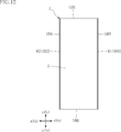
- FIG. 13 is a perspective view showing the multilayer capacitor A2.
- FIG. 14 is a plan view showing the multilayer capacitor A2.
- FIG. 15 is a bottom view showing the multilayer capacitor A2.
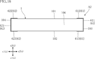
- FIG. 16 is a front view showing the multilayer capacitor A2.
- FIG. 17 is a rear view showing the multilayer capacitor A2.
- FIG. 18 is a left side view showing the multilayer capacitor A2.
- FIG. 19 is a right side view showing the multilayer capacitor A2.
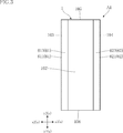
- FIG. 20 is a cross-sectional view taken along the line XX-XX of FIG.
- FIG. 21 is a plan view showing each of the first conductor layers 2 according to the second embodiment.
- FIG. 22 is a plan view showing each dielectric layer 4 according to the second embodiment.
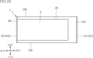
- FIG. 23 is a plan view showing each of the second conductor layers 3 according to the second embodiment.
- FIG. 24 is a plan view showing each insulating layer 5 according to the second embodiment.
- the multilayer capacitor A2 is a substantially rectangular parallelepiped like the multilayer capacitor A1.
- the laminated capacitor A2 has a rectangular shape in the longitudinal direction in the x direction and the lateral direction in the y direction in a plan view.
- the laminate 1 (a plurality of first conductor layers 2, a plurality of second conductor layers 3, a plurality of dielectric layers 4 and a plurality of insulating layers 5), which are components of the multilayer capacitor A2, and the plurality of insulating layers 5
- the pair of external electrodes 61 and 62 are configured in the same manner as the multilayer capacitor A1.
- the plurality of dielectric layers 4 are sandwiched between the first conductor layer 2 and the second conductor layer in the z direction, respectively.
- the plurality of insulating layers 5 are sandwiched between two first conductor layers 2 (for example, first conductor layers 2b and 2c) and two second conductor layers 3 (for example, second conductor layers 3a and 3b). Some are sandwiched.
- the multilayer capacitor A2 can suppress a decrease in the dielectric strength.
- the multilayer capacitor A2 can exhibit the same effect as the above-mentioned multilayer capacitor A1.
- the multilayer capacitor according to the present disclosure is not limited to the above-described embodiment.
- the specific configuration of each part of the multilayer capacitor of the present disclosure can be freely redesigned.
Abstract
A multilayer capacitor is provided with a laminate having a first side surface and a second side surface, a first side surface covering part covering the first side surface, and a second side surface covering part covering the second side surface. The laminate is obtained by laminating, in the z-direction, a plurality of first conductor layers, a plurality of second conductor layers, a plurality of dielectric layers, and a plurality of insulation layers. Each of the plurality of first conductor layers is linked to the first side surface covering part and set away from the second side surface covering part. Each of the plurality of second conductor layers is linked to the second side surface covering part and set away from the first side surface covering part. The plurality of insulation layers has a lower dielectric strength than each of the plurality of dielectric layers. Each of the plurality of dielectric layers is sandwiched by a first conductor layer and a second conductor layer 3. The plurality of insulation layers include an insulation layer sandwiched by two first conductor layers 2 and an insulation layer sandwiched by two second conductor layers 3.
Description
本開示は、積層型コンデンサに関する。
This disclosure relates to multilayer capacitors.
従来、車両や産業用機械等に組み込まれている電力変換装置(インバータ等)の電子回路が知られている。このような電子回路には、たとえば電圧の平滑化等を目的として、コンデンサが利用される。特許文献1には、従来の積層型コンデンサが開示されている。特許文献1に記載の積層型コンデンサは、複数の第1の内部電極、複数の第2の内部電極、複数の誘電体膜、複数の絶縁材、および、一対の外部電極を備えている。各第1の内部電極および各第2の内部電極はそれぞれ、金属膜である。複数の第1の内部電極は、一対の外部電極の一方で繋がっており、複数の第2の内部電極は、一対の外部電極の他方で繋がっている。複数の第1の内部電極と複数の第2の内部電極とは、積層型コンデンサの通電時に、互いに逆極性となる。各絶縁膜は、たとえば3フッ化塩化エチレン樹脂などの可塑性高分子膜である。この積層型コンデンサにおいて、各絶縁膜、各第1の内部電極、各誘電体膜、および、各第2の内部電極の順に積層され、この積層体が複数重ねられて構成されている。よって、各絶縁膜は、各第1の内部電極と各第2の内部電極とに挟まれて、これらを絶縁している。
Conventionally, electronic circuits of power conversion devices (inverters, etc.) incorporated in vehicles, industrial machines, etc. are known. Capacitors are used in such electronic circuits, for example, for the purpose of voltage smoothing. Patent Document 1 discloses a conventional multilayer capacitor. The multilayer capacitor described in Patent Document 1 includes a plurality of first internal electrodes, a plurality of second internal electrodes, a plurality of dielectric films, a plurality of insulating materials, and a pair of external electrodes. Each of the first internal electrodes and each of the second internal electrodes is a metal film. The plurality of first internal electrodes are connected by one of the pair of external electrodes, and the plurality of second internal electrodes are connected by the other of the pair of external electrodes. The plurality of first internal electrodes and the plurality of second internal electrodes have opposite polarities to each other when the multilayer capacitor is energized. Each insulating film is a plastic polymer film such as ethylene trifluoride chloride resin. In this laminated capacitor, each insulating film, each first internal electrode, each dielectric film, and each second internal electrode are laminated in this order, and a plurality of these laminated bodies are laminated. Therefore, each insulating film is sandwiched between each first internal electrode and each second internal electrode to insulate them.
特許文献1に記載の積層型コンデンサにおいては、第1の内部電極と第2の内部電極とに電位差が生じたとき、誘電体層だけでなく、絶縁膜にも電圧がかかる。そのため、この積層型コンデンサの絶縁耐力は、誘電体層の絶縁耐力あるいは絶縁膜の絶縁耐力のいずれか低いほうに制限される。特に、絶縁膜の絶縁耐力が誘電体層の絶縁耐力よりも低い場合においては、積層型コンデンサの絶縁耐力を低下させていた。
In the multilayer capacitor described in Patent Document 1, when a potential difference occurs between the first internal electrode and the second internal electrode, a voltage is applied not only to the dielectric layer but also to the insulating film. Therefore, the dielectric strength of this laminated capacitor is limited to the lower of the dielectric strength of the dielectric layer and the dielectric strength of the insulating film. In particular, when the dielectric strength of the insulating film is lower than the dielectric strength of the dielectric layer, the dielectric strength of the multilayer capacitor is lowered.
本開示は、上記事情に鑑みて考え出されたものであり、絶縁耐力の低下を抑制可能な積層型コンデンサを提供することを一の課題とする。
This disclosure was conceived in view of the above circumstances, and one of the problems is to provide a multilayer capacitor capable of suppressing a decrease in dielectric strength.
本開示によって提供される積層型コンデンサは、第1方向において互いに反対側を向く主面および裏面を有し、かつ、前記第1方向に直交する第2方向において互いに反対側を向く第1側面および第2側面を有する積層体と、前記第1側面を覆う第1側面電極と、前記第2側面を覆う第2側面電極と、を備えている。前記積層体は、複数の導体層と、複数の誘電体層と、複数の絶縁層とが前記第1方向に積層されている。前記複数の導体層は、互いに前記第1方向に離隔した複数の第1導体層および複数の第2導体層を含み、前記複数の第1導体層の各々は、前記第1側面電極に繋がり、かつ、前記第2側面電極から離隔する。前記複数の第2導体層の各々は、前記第2側面電極に繋がり、かつ、前記第1側面電極から離隔する。前記複数の絶縁層の各々は、前記複数の誘電体層の各々よりも絶縁耐力が低い。前記複数の誘電体層の各々は、前記複数の第1導体層の各々と前記複数の第2導体層の各々とに挟まれている。前記複数の絶縁層には、前記第1方向に隣接する2つの前記誘電体層の間において、2つの前記第1導体層に挟まれたものと、前記第1方向に隣接する2つの前記誘電体層の間において、2つの前記第2導体層に挟まれたものとがある。
The multilayer capacitor provided by the present disclosure has a main surface and a back surface that face each other in the first direction, and a first side surface and a back surface that face each other in the second direction orthogonal to the first direction. It includes a laminate having a second side surface, a first side surface electrode covering the first side surface, and a second side surface electrode covering the second side surface. In the laminated body, a plurality of conductor layers, a plurality of dielectric layers, and a plurality of insulating layers are laminated in the first direction. The plurality of conductor layers include a plurality of first conductor layers and a plurality of second conductor layers separated from each other in the first direction, and each of the plurality of first conductor layers is connected to the first side electrode. And, it is separated from the second side electrode. Each of the plurality of second conductor layers is connected to the second side surface electrode and separated from the first side surface electrode. Each of the plurality of insulating layers has a lower dielectric strength than each of the plurality of dielectric layers. Each of the plurality of dielectric layers is sandwiched between each of the plurality of first conductor layers and each of the plurality of second conductor layers. The plurality of insulating layers include one sandwiched between the two first conductor layers between the two dielectric layers adjacent to the first direction and the two dielectric layers adjacent to the first direction. There is one sandwiched between the two second conductor layers between the body layers.
好ましくは、前記複数の誘電体層の各々は、前記第1側面電極および前記第2側面電極の両方に接している。
Preferably, each of the plurality of dielectric layers is in contact with both the first side electrode and the second side electrode.
好ましくは、前記複数の誘電体層の各々は、前記第1方向および前記第2方向に直交する第3方向において、前記積層体の一方側の端縁から他方側の端縁まで繋がる。
Preferably, each of the plurality of dielectric layers is connected from one end edge to the other end edge of the laminate in the first direction and the third direction orthogonal to the second direction.
好ましくは、前記第2方向において、前記複数の第1導体層の各々と前記第2側面電極との間には、前記複数の絶縁層の材料と同じ材料の絶縁体が配置されている。
Preferably, in the second direction, an insulator made of the same material as the material of the plurality of insulating layers is arranged between each of the plurality of first conductor layers and the second side electrode.
好ましくは、前記第2方向において、前記複数の第2導体層の各々と前記第1側面電極との間には、前記複数の絶縁層の材料と同じ材料の絶縁体が配置されている。
Preferably, in the second direction, an insulator made of the same material as the material of the plurality of insulating layers is arranged between each of the plurality of second conductor layers and the first side electrode.
本開示の積層型コンデンサによれば、絶縁耐力の低下を抑制することができる。
According to the multilayer capacitor of the present disclosure, it is possible to suppress a decrease in dielectric strength.
本開示の積層型コンデンサの好ましい実施の形態について、図面を参照して、以下に説明する。以下の説明において、同一あるいは類似の構成要素には、同じ符号を付して、重複する説明を省略する。
A preferred embodiment of the multilayer capacitor of the present disclosure will be described below with reference to the drawings. In the following description, the same or similar components will be designated by the same reference numerals, and duplicate description will be omitted.
<第1実施形態>
図1~図12は、第1実施形態にかかる積層型コンデンサA1を示している。積層型コンデンサA1は、積層体1および一対の外部電極61,62を備えている。積層体1は、複数の第1導体層2、複数の第2導体層3、複数の誘電体層4および複数の絶縁層5を含んでいる。 <First Embodiment>
1 to 12 show the multilayer capacitor A1 according to the first embodiment. The laminated capacitor A1 includes a laminatedbody 1 and a pair of external electrodes 61 and 62. The laminate 1 includes a plurality of first conductor layers 2, a plurality of second conductor layers 3, a plurality of dielectric layers 4, and a plurality of insulating layers 5.
図1~図12は、第1実施形態にかかる積層型コンデンサA1を示している。積層型コンデンサA1は、積層体1および一対の外部電極61,62を備えている。積層体1は、複数の第1導体層2、複数の第2導体層3、複数の誘電体層4および複数の絶縁層5を含んでいる。 <First Embodiment>
1 to 12 show the multilayer capacitor A1 according to the first embodiment. The laminated capacitor A1 includes a laminated
図1は、積層型コンデンサA1を示す斜視図である。図2は、積層型コンデンサA1を示す平面図である。図3は、積層型コンデンサA1を示す底面図である。図4は積層型コンデンサA1を示す正面図である。図5は、積層型コンデンサA1を示す背面図である。図6は、積層型コンデンサA1を示す左側面図である。図7は、積層型コンデンサA1を示す右側面図である。図8は、図2のVIII-VIII線に沿う断面図である。図9は、各第1導体層2を示す平面図である。図10は、各誘電体層4を示す平面図である。図11は、各第2導体層3を示す平面図である。図12は、各絶縁層5を示す平面図である。
FIG. 1 is a perspective view showing a multilayer capacitor A1. FIG. 2 is a plan view showing the multilayer capacitor A1. FIG. 3 is a bottom view showing the multilayer capacitor A1. FIG. 4 is a front view showing the multilayer capacitor A1. FIG. 5 is a rear view showing the multilayer capacitor A1. FIG. 6 is a left side view showing the multilayer capacitor A1. FIG. 7 is a right side view showing the multilayer capacitor A1. FIG. 8 is a cross-sectional view taken along the line VIII-VIII of FIG. FIG. 9 is a plan view showing each first conductor layer 2. FIG. 10 is a plan view showing each dielectric layer 4. FIG. 11 is a plan view showing each second conductor layer 3. FIG. 12 is a plan view showing each insulating layer 5.
説明の便宜上、互いに直交する3つの方向を、x方向、y方向、z方向とする。z方向は、積層型コンデンサA1の厚さ方向である。x方向は、積層型コンデンサA1の平面図(図2参照)における左右方向である。y方向は、積層型コンデンサA1の平面図(図2参照)における上下方向である。x方向の一方をx1方向、x方向の他方をx2方向とする。同様に、y方向の一方をy1方向、y方向の他方をy2方向とし、z方向の一方をz1方向、z方向の他方をz2方向とする。以下の説明において、「平面視」とは、z方向に見たときをいう。z方向が、「第1方向」の一例であり、x方向が、「第2方向」の一例であり、y方向が、「第3方向」の一例である。
For convenience of explanation, the three directions orthogonal to each other are the x direction, the y direction, and the z direction. The z direction is the thickness direction of the multilayer capacitor A1. The x direction is the left-right direction in the plan view (see FIG. 2) of the multilayer capacitor A1. The y direction is the vertical direction in the plan view (see FIG. 2) of the multilayer capacitor A1. One in the x direction is the x1 direction, and the other in the x direction is the x2 direction. Similarly, one in the y direction is the y1 direction, the other in the y direction is the y2 direction, one in the z direction is the z1 direction, and the other in the z direction is the z2 direction. In the following description, "planar view" means when viewed in the z direction. The z direction is an example of the "first direction", the x direction is an example of the "second direction", and the y direction is an example of the "third direction".
積層体1は、たとえば略直方体である。積層体1は、図2に示すように、平面視において、x方向が短手方向、y方向が長手方向の矩形状である。積層体1は、主面101、裏面102、および、複数の側面103~106を有している。
The laminated body 1 is, for example, a substantially rectangular parallelepiped. As shown in FIG. 2, the laminated body 1 has a rectangular shape in a plan view in which the x direction is the lateral direction and the y direction is the longitudinal direction. The laminated body 1 has a main surface 101, a back surface 102, and a plurality of side surfaces 103 to 106.
主面101および裏面102は、図4~図8に示すように、z方向に離隔している。主面101は、z2方向を向き、裏面102は、z1方向を向く。複数の側面103~106はそれぞれ、図4~図8に示すように、z方向において主面101と裏面102との間に位置し、かつ、主面101および裏面102にそれぞれ繋がっている。側面103および側面104は、図2および図3に示すように、x方向に離隔する。側面103は、x2方向を向き、側面104は、x1方向を向く。側面105および側面106は、図2および図3に示すように、y方向に離隔する。側面105は、y2方向を向き、側面106は、y1方向を向く。側面103が、「第1側面」の一例であり、側面104が、「第2側面」の一例である。
The main surface 101 and the back surface 102 are separated in the z direction as shown in FIGS. 4 to 8. The main surface 101 faces the z2 direction, and the back surface 102 faces the z1 direction. As shown in FIGS. 4 to 8, the plurality of side surfaces 103 to 106 are located between the main surface 101 and the back surface 102 in the z direction, and are connected to the main surface 101 and the back surface 102, respectively. The side surface 103 and the side surface 104 are separated in the x direction as shown in FIGS. 2 and 3. The side surface 103 faces the x2 direction, and the side surface 104 faces the x1 direction. The side surfaces 105 and 106 are separated in the y direction, as shown in FIGS. 2 and 3. The side surface 105 faces the y2 direction, and the side surface 106 faces the y1 direction. The side surface 103 is an example of the "first side surface", and the side surface 104 is an example of the "second side surface".
積層体1は、上述の通り、複数の第1導体層2、複数の第2導体層3、複数の誘電体層4および複数の絶縁層5を含んでいる。本実施形態においては、図8に示すように、積層体1は、3つの第1導体層2a~2c、3つの第2導体層3a~3c、3つの誘電体層4a~4cおよび4つの絶縁層5a~5dを含んでいる。複数の第1導体層2、複数の第2導体層3、複数の誘電体層4および複数の絶縁層5は、後に詳説する構成により、z方向に積層されている。複数の第1導体層2と複数の第2導体層3とを合わせたものが、「複数の導体層」の一例である。
As described above, the laminate 1 includes a plurality of first conductor layers 2, a plurality of second conductor layers 3, a plurality of dielectric layers 4, and a plurality of insulating layers 5. In the present embodiment, as shown in FIG. 8, the laminate 1 has three first conductor layers 2a to 2c, three second conductor layers 3a to 3c, three dielectric layers 4a to 4c, and four insulations. It contains layers 5a-5d. The plurality of first conductor layers 2, the plurality of second conductor layers 3, the plurality of dielectric layers 4, and the plurality of insulating layers 5 are laminated in the z direction according to the configuration described in detail later. A combination of the plurality of first conductor layers 2 and the plurality of second conductor layers 3 is an example of the "plurality of conductor layers".
複数の第1導体層2はそれぞれ、たとえばCuからなる。各第1導体層2の厚さは、たとえば30μm以上70μm以下である。各第1導体層2は、図8に示すように、x2方向側の端縁が側面103から露出している。複数の第1導体層2は、平面視において、互 いに重なる。各第1導体層2は、図9に示すように、平面視において、積層体1のx2方向側の端縁からx1方向に向かって延びている。各第1導体層2は、図9に示すように、x2方向側の端縁が側面103から露出しており、x1方向側の端縁が側面104から露出していない。よって、平面視において、各第1導体層2は、x1方向側の端縁が、側面104よりも積層体1の内方に位置する。また、各第1導体層2は、図9に示すように、平面視において、側面105および側面106のいずれからも露出していない。よって、平面視において、各第1導体層2は、y1方向側の端縁が、側面106よりも積層体1の内方に位置し、y2方向側の端縁が、側面105よりも積層体1の内方に位置する。
Each of the plurality of first conductor layers 2 is made of, for example, Cu. The thickness of each first conductor layer 2 is, for example, 30 μm or more and 70 μm or less. As shown in FIG. 8, each first conductor layer 2 has an edge on the x2 direction side exposed from the side surface 103. The plurality of first conductor layers 2 overlap each other in a plan view. As shown in FIG. 9, each first conductor layer 2 extends from the edge of the laminated body 1 on the x2 direction side toward the x1 direction in a plan view. As shown in FIG. 9, each first conductor layer 2 has an edge on the x2 direction side exposed from the side surface 103 and an edge on the x1 direction side not exposed from the side surface 104. Therefore, in a plan view, the edge of each first conductor layer 2 on the x1 direction side is located inside the laminated body 1 with respect to the side surface 104. Further, as shown in FIG. 9, each first conductor layer 2 is not exposed from either the side surface 105 or the side surface 106 in a plan view. Therefore, in a plan view, the edge of each first conductor layer 2 on the y1 direction side is located inside the laminated body 1 with respect to the side surface 106, and the edge on the y2 direction side is the laminated body with respect to the side surface 105. It is located inside 1.
図9に示すように、平面視において、各第1導体層2の周囲(x2方向側の端縁を除く)には、絶縁体29が形成されている。具体的には、絶縁体29は、各第1導体層2と側面104との間、各第1導体層2と側面105との間、および、各第1導体層2と側面106との間に位置する。絶縁体29は、後述する絶縁層5と同じ材料である。
As shown in FIG. 9, in a plan view, an insulator 29 is formed around each first conductor layer 2 (excluding the edge on the x2 direction side). Specifically, the insulator 29 is provided between the first conductor layer 2 and the side surface 104, between the first conductor layer 2 and the side surface 105, and between the first conductor layer 2 and the side surface 106. Located in. The insulator 29 is made of the same material as the insulating layer 5 described later.
複数の第2導体層3はそれぞれ、たとえばCuからなる。各第2導体層3の厚さは、たとえば30μm以上70μm以下である。各第2導体層3は、図8に示すように、x1方向側の端縁が側面104から露出している。複数の第2導体層3は、平面視において、互いに重なる。各第2導体層3は、図11に示すように、平面視において、積層体1のx1方向側の端縁からx2方向に向かって延びている。各第2導体層3は、図11に示すように、x1方向側の端縁が側面104から露出しており、x2方向側の端縁が側面103から露出していない。よって、平面視において、各第2導体層3は、x2方向側の端縁が、側面103よりも積層体1の内方に位置する。また、各第2導体層3は、図11に示すように、平面視において、側面105および側面106のいずれからも露出していない。よって、平面視において、各第2導体層3は、y1方向側の端縁が、側面106よりも積層体1の内方に位置し、y2方向側の端縁が、側面105よりも積層体1の内方に位置する。
Each of the plurality of second conductor layers 3 is made of, for example, Cu. The thickness of each second conductor layer 3 is, for example, 30 μm or more and 70 μm or less. As shown in FIG. 8, each second conductor layer 3 has an edge on the x1 direction side exposed from the side surface 104. The plurality of second conductor layers 3 overlap each other in a plan view. As shown in FIG. 11, each second conductor layer 3 extends from the edge of the laminated body 1 on the x1 direction side toward the x2 direction in a plan view. As shown in FIG. 11, each second conductor layer 3 has an edge on the x1 direction side exposed from the side surface 104 and an edge on the x2 direction side not exposed from the side surface 103. Therefore, in a plan view, the edge of each second conductor layer 3 on the x2 direction side is located inside the laminated body 1 with respect to the side surface 103. Further, as shown in FIG. 11, each second conductor layer 3 is not exposed from either the side surface 105 or the side surface 106 in a plan view. Therefore, in a plan view, the edge of each second conductor layer 3 on the y1 direction side is located inside the laminated body 1 with respect to the side surface 106, and the edge on the y2 direction side is the laminated body with respect to the side surface 105. It is located inside 1.
図11に示すように、平面視において、各第2導体層3の周囲(x1方向側の端縁を除く)には、絶縁体39が形成されている。具体的には、絶縁体39は、各第2導体層3と側面103との間、各第2導体層3と側面105との間、および、各第2導体層3と側面106との間に位置する。絶縁体39は、絶縁体29と同じ材料である。つまり、絶縁体39は、後述する絶縁層5と同じ材料である。
As shown in FIG. 11, in a plan view, an insulator 39 is formed around each second conductor layer 3 (excluding the edge on the x1 direction side). Specifically, the insulator 39 is provided between the second conductor layer 3 and the side surface 103, between the second conductor layer 3 and the side surface 105, and between the second conductor layer 3 and the side surface 106. Located in. The insulator 39 is made of the same material as the insulator 29. That is, the insulator 39 is the same material as the insulating layer 5 described later.
複数の第1導体層2と複数の第2導体層3とは、平面視において、部分的に重なる。また、複数の第1導体層2と複数の第2導体層3とは、積層型コンデンサA1の通電時において、互いに逆極性となる。
The plurality of first conductor layers 2 and the plurality of second conductor layers 3 partially overlap in a plan view. Further, the plurality of first conductor layers 2 and the plurality of second conductor layers 3 have opposite polarities to each other when the laminated capacitor A1 is energized.
各誘電体層4は、各第1導体層2と各第2導体層3とに挟まれている。図8に示す例では、誘電体層4aは、第1導体層2aと第2導体層3aとに挟まれている。誘電体層4bは、第2導体層3bと第1導体層2bとに挟まれている。誘電体層4cは、第1導体層2cと第2導体層3cとに挟まれている。図10に示すように、各誘電体層4は、平面視において、積層体1のx1方向側の端縁からx2方向側の端縁まで繋がっており、かつ、積層体1のy1方向側の端縁からy2方向側の端縁まで繋がっている。各誘電体層4は、たとえばポリマーフィルムなどのフィルム状の樹脂材料からなる。各誘電体層4の構成材料は、フィルム状の樹脂材料に限定されず、たとえば比誘電率が1より大きい材料であればよい。このような材料としては金属酸化物ペロブスカイト化合物などを主成分とするセラミックなどが挙げられる。各誘電体層4の厚さは、たとえば8μm以上25μm以下である。
Each dielectric layer 4 is sandwiched between each first conductor layer 2 and each second conductor layer 3. In the example shown in FIG. 8, the dielectric layer 4a is sandwiched between the first conductor layer 2a and the second conductor layer 3a. The dielectric layer 4b is sandwiched between the second conductor layer 3b and the first conductor layer 2b. The dielectric layer 4c is sandwiched between the first conductor layer 2c and the second conductor layer 3c. As shown in FIG. 10, each dielectric layer 4 is connected from the edge of the laminate 1 on the x1 direction side to the edge on the x2 direction side of the laminate 1 in a plan view, and is on the y1 direction side of the laminate 1. It is connected from the edge to the edge on the y2 direction side. Each dielectric layer 4 is made of a film-like resin material such as a polymer film. The constituent material of each dielectric layer 4 is not limited to the film-shaped resin material, and may be any material having a relative permittivity of more than 1, for example. Examples of such a material include ceramics containing a metal oxide perovskite compound as a main component. The thickness of each dielectric layer 4 is, for example, 8 μm or more and 25 μm or less.
複数の絶縁層5はそれぞれ、たとえばプリプレグからなる。各絶縁層5は、z方向の両 面のそれぞれに接する2つの第1導体層2や2つの第2導体層3を絶縁する。各絶縁層5は、各誘電体層4よりも絶縁耐力が低い。また、各絶縁層5は、z方向の両面のそれぞれに接する2つの第1導体層2や2つの第2導体層3の接着層としても機能する。各絶縁層5の厚さは、たとえば40μm以上100μm以下である。
Each of the plurality of insulating layers 5 is made of, for example, a prepreg. Each insulating layer 5 insulates two first conductor layers 2 and two second conductor layers 3 in contact with each of both surfaces in the z direction. Each insulating layer 5 has a lower dielectric strength than each dielectric layer 4. In addition, each insulating layer 5 also functions as an adhesive layer of two first conductor layers 2 and two second conductor layers 3 in contact with each of both sides in the z direction. The thickness of each insulating layer 5 is, for example, 40 μm or more and 100 μm or less.
複数の絶縁層5は、図8に示すように、z方向に隣り合う2つの誘電体層4の間において、2つの第1導体層2に挟まれたものと、z方向に隣り合う2つの誘電体層4の間において、2つの第2導体層3に挟まれたものとを含む。また、複数の絶縁層5は、図8に示すように、積層体1の主面101に形成された一対の外部電極61,62(後述の主面被覆部612,622)と第1導体層2とに挟まれたものと、積層体1の裏面102に形成された一対の外部電極61,62(後述の裏面被覆部613,623)と第2導体層3とに挟まれたものとをさらに含む。図8に示す例では、絶縁層5aは、積層体1のz2方向側の表層であり、後述の主面被覆部612,622と第1導体層2aとに挟まれている。絶縁層5bは、2つの誘電体層4a,4bの間において、第2導体層3aと第2導体層3bとに挟まれている。絶縁層5cは、2つの誘電体層4b,4cの間において、第1導体層2bと第1導体層2cとに挟まれている。絶縁層5dは、積層体1のz1方向側の表層であり、後述の裏面被覆部613,623と第2導体層3cとに挟まれている。
As shown in FIG. 8, the plurality of insulating layers 5 are sandwiched between two first conductor layers 2 between two dielectric layers 4 adjacent to each other in the z direction, and two adjacent layers 5 in the z direction. Among the dielectric layers 4, the one sandwiched between the two second conductor layers 3 is included. Further, as shown in FIG. 8, the plurality of insulating layers 5 are a pair of external electrodes 61 and 62 (main surface covering portions 612 and 622 described later) and a first conductor layer formed on the main surface 101 of the laminated body 1. The one sandwiched between the two and the pair of external electrodes 61, 62 (described later, the back surface covering portions 613 and 623) formed on the back surface 102 of the laminated body 1 and the second conductor layer 3 are sandwiched between the two. Including further. In the example shown in FIG. 8, the insulating layer 5a is the surface layer of the laminated body 1 on the z2 direction side, and is sandwiched between the main surface covering portions 612 and 622 and the first conductor layer 2a, which will be described later. The insulating layer 5b is sandwiched between the second conductor layer 3a and the second conductor layer 3b between the two dielectric layers 4a and 4b. The insulating layer 5c is sandwiched between the first conductor layer 2b and the first conductor layer 2c between the two dielectric layers 4b and 4c. The insulating layer 5d is a surface layer of the laminate 1 on the z1 direction side, and is sandwiched between the back surface covering portions 613 and 623 and the second conductor layer 3c, which will be described later.
積層体1は、z方向において、第1導体層2、誘電体層4、第2導体層3の順に積層された第1ユニットと、z2方向からz1方向に向かって、第2導体層3、誘電体層4、第1導体層2の順に積層された第2ユニットとが、絶縁層5を挟んで交互に重ね合わせられている。第1ユニットと第2ユニットのそれぞれの数は、特に限定されず、第1ユニットと第2ユニットとの数が同じでなくてもよい。図8に示す例では、絶縁層5、第1ユニット、絶縁層5、第2ユニット、絶縁層5、第1ユニット、絶縁層5の順に重ね合せられている。つまり、図8に示す例では、2つの第1ユニットと、1つの第2ユニットとが、絶縁層5を挟んで、交互に重ね合わせられている。積層体1の積層構造については、上記した例に限定されず、z方向両側の各表層が誘電体層4となるように構成されていてもよい。
The laminated body 1 includes a first unit in which the first conductor layer 2, the dielectric layer 4, and the second conductor layer 3 are laminated in this order in the z direction, and the second conductor layer 3 from the z2 direction to the z1 direction. The second unit in which the dielectric layer 4 and the first conductor layer 2 are laminated in this order are alternately overlapped with the insulating layer 5 interposed therebetween. The number of each of the first unit and the second unit is not particularly limited, and the numbers of the first unit and the second unit do not have to be the same. In the example shown in FIG. 8, the insulating layer 5, the first unit, the insulating layer 5, the second unit, the insulating layer 5, the first unit, and the insulating layer 5 are superposed in this order. That is, in the example shown in FIG. 8, two first units and one second unit are alternately overlapped with the insulating layer 5 interposed therebetween. The laminated structure of the laminated body 1 is not limited to the above-mentioned example, and each surface layer on both sides in the z direction may be configured to be a dielectric layer 4.
積層体1において、各層(各第1導体層2、各第2導体層3、誘電体層4、および、絶縁層5)のx方向寸法、y方向寸法およびz方向寸法(厚さ)、各層の構成材料、各層の積層数などは、特に限定されず、積層型コンデンサA1の仕様(たとえば静電容量やサイズなど)に基づいて、適宜変更されうる。積層型コンデンサA1の静電容量Cは、C=ε0・εr・(S/d)・N[F]で算出される。この式において、ε0は真空の誘電率、εrは誘電体(各誘電体層4)の比誘電率、Sは内部電極(各第1導体層2および各第2導体層3が平面視において重なる領域)の面積、dは電極間(各第1導体層2と各第2導体層3との間)の距離、Nは誘電体層4の積層数を表す。たとえば、上記式から、各第1導体層2と各第2導体層3とのz方向の離隔距離(誘電体層4の厚さ)が大きいほど、静電容量は小さい。また、誘電体層4の比誘電率が大きいほど、静電容量は大きい。また、各第1導体層2と各第2導体層3の平面視面積が大きいほど、静電容量は大きい。また、各層の積層数(上記ユニットの数)が多いほど、静電容量は大きい。
In the laminated body 1, the x-direction dimension, the y-direction dimension and the z-direction dimension (thickness) of each layer (each first conductor layer 2, each second conductor layer 3, dielectric layer 4, and insulating layer 5), each layer. The constituent materials of the above, the number of layers of each layer, and the like are not particularly limited, and can be appropriately changed based on the specifications (for example, capacitance, size, etc.) of the multilayer capacitor A1. The capacitance C of the multilayer capacitor A1 is calculated by C = ε 0 · ε r · (S / d) · N [F]. In this equation, ε 0 is the dielectric constant of the vacuum, ε r is the relative permittivity of the dielectric (each dielectric layer 4), and S is the internal electrode (each first conductor layer 2 and each second conductor layer 3 in plan view. In, d represents the distance between the electrodes (between each first conductor layer 2 and each second conductor layer 3), and N represents the number of layers of the dielectric layer 4. For example, from the above equation, the larger the separation distance (thickness of the dielectric layer 4) in the z direction between each first conductor layer 2 and each second conductor layer 3, the smaller the capacitance. Further, the larger the relative permittivity of the dielectric layer 4, the larger the capacitance. Further, the larger the plan-view area of each of the first conductor layers 2 and each of the second conductor layers 3, the larger the capacitance. Further, the larger the number of laminated layers (the number of the above units), the larger the capacitance.
一対の外部電極61,62は、積層体1の、主面101の一部と、裏面102の一部と、各側面103,104とを覆うように形成されている。一対の外部電極61,62は、積層型コンデンサA1の端子である。一対の外部電極61,62は、互いに離隔し、互いに絶縁する。一対の外部電極61,62は、たとえばCuからなるが、これに限定されない。一対の外部電極61,62は、たとえばめっき処理により形成されるが、これに限定されない。
The pair of external electrodes 61 and 62 are formed so as to cover a part of the main surface 101, a part of the back surface 102, and the side surfaces 103 and 104 of the laminated body 1. The pair of external electrodes 61 and 62 are terminals of the multilayer capacitor A1. The pair of external electrodes 61 and 62 are separated from each other and insulated from each other. The pair of external electrodes 61, 62 is made of, for example, Cu, but is not limited thereto. The pair of external electrodes 61, 62 is formed by, for example, plating, but is not limited thereto.
外部電極61は、積層型コンデンサA1の一方の端子である。外部電極61は、側面被 覆部611、主面被覆部612および裏面被覆部613を含む。側面被覆部611は、図1~図5、図7および図8に示すように、側面103を覆う。主面被覆部612は、図1、図2、図4、図5および図8に示すように、主面101の一部を覆う。主面被覆部612は、図2に示すように、主面101のうちx2方向側の部分に形成されている。主面被覆部612は、側面被覆部611に繋がる。裏面被覆部613は、図3~図5および図8に示すように、裏面102の一部を覆う。裏面被覆部613は、図3に示すように、裏面102のうちx2方向側の部分に形成されている。裏面被覆部613は、側面被覆部611に繋がる。図8に示す例では、主面被覆部612および裏面被覆部613は、平面視において、各第2導体層3には重ならない。なお、外部電極61は、側面被覆部611、主面被覆部612および裏面被覆部613に繋がり、かつ、2つの側面105,106の一部を覆う部分をさらに含んでいてもよい。また、外部電極61は、主面被覆部612および裏面被覆部613を含んでいなくてもよい。
The external electrode 61 is one terminal of the multilayer capacitor A1. The external electrode 61 includes a side covering portion 611, a main surface covering portion 612, and a back surface covering portion 613. The side surface covering portion 611 covers the side surface 103 as shown in FIGS. 1 to 5, 7 and 8. The main surface covering portion 612 covers a part of the main surface 101 as shown in FIGS. 1, 2, 4, 5, and 8. As shown in FIG. 2, the main surface covering portion 612 is formed on the portion of the main surface 101 on the x2 direction side. The main surface covering portion 612 is connected to the side covering portion 611. The back surface covering portion 613 covers a part of the back surface 102 as shown in FIGS. 3 to 5 and 8. As shown in FIG. 3, the back surface covering portion 613 is formed on the back surface 102 on the x2 direction side. The back surface covering portion 613 is connected to the side surface covering portion 611. In the example shown in FIG. 8, the main surface covering portion 612 and the back surface covering portion 613 do not overlap each of the second conductor layers 3 in a plan view. The external electrode 61 may further include a portion that is connected to the side surface covering portion 611, the main surface covering portion 612, and the back surface covering portion 613 and that partially covers the two side surfaces 105 and 106. Further, the external electrode 61 may not include the main surface covering portion 612 and the back surface covering portion 613.
上述の通り、側面103と各第2導体層3との間に絶縁体39が配置されていることから、図11に示すように、x方向において、側面被覆部611と各第2導体層3との間には、各絶縁体39が配置されている。よって、各絶縁体39により、側面被覆部611と各第2導体層3とが絶縁される。また、図8および図9に示すように、側面被覆部611は、各第1導体層2のx2方向側の端縁に接していることから、側面被覆部611は、z方向に離隔して配置された複数の第1導体層2を電気的に繋いでいる。よって、側面被覆部611を介して、複数の第1導体層2が互いに同電位となる。側面被覆部611が、「第1側面電極」の一例である。
As described above, since the insulator 39 is arranged between the side surface 103 and each of the second conductor layers 3, as shown in FIG. 11, the side surface covering portion 611 and each of the second conductor layers 3 are arranged in the x direction. Each insulator 39 is arranged between and. Therefore, each insulator 39 insulates the side surface covering portion 611 and each second conductor layer 3. Further, as shown in FIGS. 8 and 9, since the side surface covering portion 611 is in contact with the edge of each first conductor layer 2 on the x2 direction side, the side surface covering portion 611 is separated in the z direction. A plurality of arranged first conductor layers 2 are electrically connected. Therefore, the plurality of first conductor layers 2 have the same potential with each other via the side surface covering portion 611. The side surface covering portion 611 is an example of the “first side surface electrode”.
外部電極62は、積層型コンデンサA1の他方の端子である。外部電極62は、側面被覆部621、主面被覆部622および裏面被覆部623を含む。側面被覆部621は、図2~図6および図8に示すように、側面104を覆う。主面被覆部622は、図2、図4、図5および図8に示すように、主面101の一部を覆う。主面被覆部622は、図2に示すように、主面101のうちx1方向側の部分に形成されており、主面被覆部612(外部電極61)から離隔する。主面被覆部622は、側面被覆部621に繋がる。裏面被覆部623は、図3~図5および図8に示すように、裏面102の一部を覆う。裏面被覆部623は、裏面102のうちx1方向側の部分に形成されており、裏面被覆部613(外部電極61)から離隔する。裏面被覆部623は、側面被覆部621に繋がる。図8に示す例では、主面被覆部622および裏面被覆部623は、平面視において、各第1導体層2には重ならない。なお、外部電極62は、側面被覆部621、主面被覆部622および裏面被覆部623に繋がり、かつ、2つの側面105,106の一部を覆う部分をさらに含んでいてもよい。また、外部電極62は、主面被覆部622および裏面被覆部623を含んでいなくてもよい。
The external electrode 62 is the other terminal of the multilayer capacitor A1. The external electrode 62 includes a side surface covering portion 621, a main surface covering portion 622, and a back surface covering portion 623. The side covering portion 621 covers the side surface 104 as shown in FIGS. 2 to 6 and 8. The main surface covering portion 622 covers a part of the main surface 101 as shown in FIGS. 2, 4, 5, and 8. As shown in FIG. 2, the main surface covering portion 622 is formed on the portion of the main surface 101 on the x1 direction side, and is separated from the main surface covering portion 612 (external electrode 61). The main surface covering portion 622 is connected to the side covering portion 621. The back surface covering portion 623 covers a part of the back surface 102 as shown in FIGS. 3 to 5 and 8. The back surface covering portion 623 is formed on the portion of the back surface 102 on the x1 direction side, and is separated from the back surface covering portion 613 (external electrode 61). The back surface covering portion 623 is connected to the side surface covering portion 621. In the example shown in FIG. 8, the main surface covering portion 622 and the back surface covering portion 623 do not overlap each of the first conductor layers 2 in a plan view. The external electrode 62 may further include a portion connected to the side surface covering portion 621, the main surface covering portion 622, and the back surface covering portion 623, and further covering a part of the two side surfaces 105 and 106. Further, the external electrode 62 does not have to include the main surface covering portion 622 and the back surface covering portion 623.
上述の通り、側面104と各第1導体層2との間に絶縁体29が配置されていることから、図9に示すように、x方向において、側面被覆部621と各第1導体層2との間には、各絶縁体29が配置されている。よって、各絶縁体29により、側面被覆部621と各第1導体層2とが絶縁される。また、図8および図11に示すように、側面被覆部621は、各第2導体層3のx1方向側の端縁に接していることから、側面被覆部621は、z方向に離隔して配置された複数の第2導体層3を電気的に繋いでいる。よって、側面被覆部621を介して、複数の第2導体層3が互いに同電位となる。側面被覆部621が、「第2側面電極」の一例である。
As described above, since the insulator 29 is arranged between the side surface 104 and each of the first conductor layers 2, as shown in FIG. 9, the side surface covering portion 621 and each of the first conductor layers 2 are arranged in the x direction. Each insulator 29 is arranged between and. Therefore, each insulator 29 insulates the side surface covering portion 621 and each first conductor layer 2. Further, as shown in FIGS. 8 and 11, since the side surface covering portion 621 is in contact with the edge of each second conductor layer 3 on the x1 direction side, the side surface covering portion 621 is separated in the z direction. A plurality of arranged second conductor layers 3 are electrically connected. Therefore, the plurality of second conductor layers 3 have the same potential with each other via the side surface covering portion 621. The side surface covering portion 621 is an example of the “second side surface electrode”.
積層型コンデンサA1の作用および効果は、次の通りである。
The actions and effects of the multilayer capacitor A1 are as follows.
積層型コンデンサA1では、複数の誘電体層4はそれぞれ、z方向において、各第1導体層2と各第2導体層3とに挟まれている。複数の絶縁層5には、z方向に隣接する2つ の誘電体層4(たとえば誘電体層4b,4c)の間において、2つの第1導体層2(たとえば第1導体層2b,2c)に挟まれたものと、z方向に隣接する2つの誘電体層4(たとえば誘電体層4a,4b)の間において、2つの第2導体層3(たとえば第2導体層3a,3b)に挟まれたものとがある。各絶縁層5は、各誘電体層4よりも絶縁耐力が低い。この構成によると、誘電体層4は、電位の異なる2つの導体層(第1導体層2と第2導体層3)に挟まれ、絶縁層5は、電位が同じ2つの導体層(2つの第1導体層2、あるいは、2つの第2導体層3)に挟まれた構成となる。したがって、積層型コンデンサA1の通電時に、複数の第1導体層2と複数の第2導体層3とに電位差が生じたとき、誘電体層4の厚さ方向(z方向)には電圧がかかるが、絶縁層5の厚さ方向(z方向)には電圧がかからない。そのため、絶縁層5の耐電圧(絶縁耐力)を保証しなくてもよい。つまり、積層型コンデンサA1は、絶縁耐力の低下を抑制することができる。
In the laminated capacitor A1, the plurality of dielectric layers 4 are sandwiched between the first conductor layer 2 and the second conductor layer 3 in the z direction, respectively. The plurality of insulating layers 5 include two first conductor layers 2 (for example, first conductor layers 2b and 2c) between two dielectric layers 4 (for example, dielectric layers 4b and 4c) adjacent to each other in the z direction. It is sandwiched between two second conductor layers 3 (for example, second conductor layers 3a and 3b) between two dielectric layers 4 (for example, dielectric layers 4a and 4b) adjacent to each other in the z direction. There is something that has been done. Each insulating layer 5 has a lower dielectric strength than each dielectric layer 4. According to this configuration, the dielectric layer 4 is sandwiched between two conductor layers (first conductor layer 2 and second conductor layer 3) having different potentials, and the insulating layer 5 is two conductor layers (two conductor layers) having the same potential. The structure is sandwiched between the first conductor layer 2 or two second conductor layers 3). Therefore, when a potential difference occurs between the plurality of first conductor layers 2 and the plurality of second conductor layers 3 when the multilayer capacitor A1 is energized, a voltage is applied to the thickness direction (z direction) of the dielectric layer 4. However, no voltage is applied in the thickness direction (z direction) of the insulating layer 5. Therefore, it is not necessary to guarantee the withstand voltage (dielectric strength) of the insulating layer 5. That is, the multilayer capacitor A1 can suppress a decrease in the dielectric strength.
積層型コンデンサA1では、たとえば、誘電体層4は、樹脂材料であり、絶縁層5は、プリプレグである。従来の積層型コンデンサには、誘電体層4がセラミックで構成されたセラミックコンデンサがある。セラミックは、その物性上、熱応力などのストレスにより割れやすい。そのため、セラミックコンデンサは、その通電時に生じる発熱により、誘電体層4にクラックなどの破壊が生じる可能性がある。この破壊により、誘電体層4の絶縁耐力が低下する。一方、本開示の積層型コンデンサA1においては、誘電体層4が、セラミックではないため、熱応力によるクラックなどの発生を抑制できる。したがって、積層型コンデンサA1は、絶縁耐力の低下を抑制することができる。
In the multilayer capacitor A1, for example, the dielectric layer 4 is a resin material, and the insulating layer 5 is a prepreg. Conventional multilayer capacitors include ceramic capacitors in which the dielectric layer 4 is made of ceramic. Due to its physical properties, ceramics are easily cracked by stress such as thermal stress. Therefore, in the ceramic capacitor, the dielectric layer 4 may be cracked or otherwise broken due to the heat generated when the ceramic capacitor is energized. Due to this destruction, the dielectric strength of the dielectric layer 4 is lowered. On the other hand, in the multilayer capacitor A1 of the present disclosure, since the dielectric layer 4 is not ceramic, the occurrence of cracks due to thermal stress can be suppressed. Therefore, the multilayer capacitor A1 can suppress a decrease in the dielectric strength.
積層型コンデンサA1では、各第1導体層2は、y1方向側の端縁およびy2方向側の端縁がそれぞれ、絶縁体29で覆われている。また、各第2導体層3は、y1方向側の端縁およびy2方向側の端縁がそれぞれ、絶縁体39で覆われている。この構成によると、各第1導体層2および各第2導体層3はそれぞれ、積層体1の各側面105,106において露出しない。したがって、各側面105,106で、各第1導体層2と各第2導体層3とが意図せぬ短絡が発生することを抑制できる。
In the laminated capacitor A1, each of the first conductor layers 2 is covered with an insulator 29 at the edge on the y1 direction side and the edge on the y2 direction side, respectively. Further, in each of the second conductor layers 3, the edge on the y1 direction side and the edge on the y2 direction side are each covered with an insulator 39. According to this configuration, the first conductor layer 2 and the second conductor layer 3 are not exposed on the side surfaces 105 and 106 of the laminated body 1, respectively. Therefore, it is possible to prevent an unintended short circuit between the first conductor layer 2 and the second conductor layer 3 on the side surfaces 105 and 106.
<第2実施形態>
図13~図24は、第2実施形態にかかる積層型コンデンサA2を示している。 <Second Embodiment>
13 to 24 show the multilayer capacitor A2 according to the second embodiment.
図13~図24は、第2実施形態にかかる積層型コンデンサA2を示している。 <Second Embodiment>
13 to 24 show the multilayer capacitor A2 according to the second embodiment.
図13は、積層型コンデンサA2を示す斜視図である。図14は、積層型コンデンサA2を示す平面図である。図15は、積層型コンデンサA2を示す底面図である。図16は積層型コンデンサA2を示す正面図である。図17は、積層型コンデンサA2を示す背面図である。図18は、積層型コンデンサA2を示す左側面図である。図19は、積層型コンデンサA2を示す右側面図である。図20は、図14のXX-XX線に沿う断面図である。図21は、第2実施形態にかかる各第1導体層2を示す平面図である。図22は、第2実施形態にかかる各誘電体層4を示す平面図である。図23は、第2実施形態にかかる各第2導体層3を示す平面図である。図24は、第2実施形態にかかる各絶縁層5を示す平面図である。
FIG. 13 is a perspective view showing the multilayer capacitor A2. FIG. 14 is a plan view showing the multilayer capacitor A2. FIG. 15 is a bottom view showing the multilayer capacitor A2. FIG. 16 is a front view showing the multilayer capacitor A2. FIG. 17 is a rear view showing the multilayer capacitor A2. FIG. 18 is a left side view showing the multilayer capacitor A2. FIG. 19 is a right side view showing the multilayer capacitor A2. FIG. 20 is a cross-sectional view taken along the line XX-XX of FIG. FIG. 21 is a plan view showing each of the first conductor layers 2 according to the second embodiment. FIG. 22 is a plan view showing each dielectric layer 4 according to the second embodiment. FIG. 23 is a plan view showing each of the second conductor layers 3 according to the second embodiment. FIG. 24 is a plan view showing each insulating layer 5 according to the second embodiment.
図13に示すように、積層型コンデンサA2は、積層型コンデンサA1と同様に略直方体である。ただし、図13~図24に示すように、積層型コンデンサA2は、積層型コンデンサA1と異なり、平面視において、x方向が長手方向、y方向が短手方向の矩形状である。この点を除いて、積層型コンデンサA2の各構成要素である積層体1(複数の第1導体層2、複数の第2導体層3、複数の誘電体層4および複数の絶縁層5)および一対の外部電極61,62は、積層型コンデンサA1と同様に構成されている。
As shown in FIG. 13, the multilayer capacitor A2 is a substantially rectangular parallelepiped like the multilayer capacitor A1. However, as shown in FIGS. 13 to 24, unlike the laminated capacitor A1, the laminated capacitor A2 has a rectangular shape in the longitudinal direction in the x direction and the lateral direction in the y direction in a plan view. Except for this point, the laminate 1 (a plurality of first conductor layers 2, a plurality of second conductor layers 3, a plurality of dielectric layers 4 and a plurality of insulating layers 5), which are components of the multilayer capacitor A2, and the plurality of insulating layers 5 The pair of external electrodes 61 and 62 are configured in the same manner as the multilayer capacitor A1.
積層型コンデンサA2においても、積層型コンデンサA1と同様に、複数の誘電体層4はそれぞれ、z方向において、各第1導体層2と各第2導体層とに挟まれている。複数の 絶縁層5には、2つの第1導体層2(たとえば第1導体層2b,2c)に挟まれたものと、2つの第2導体層3(たとえば第2導体層3a,3b)に挟まれたものとがある。したがって、複数の第1導体層2と複数の第2導体層3とに電位差が生じたとき、誘電体層4の厚さ方向(z方向)には電圧がかかるが、絶縁層5の厚さ方向(z方向)には電圧がかからないため、絶縁層5の耐電圧(絶縁耐力)を保証しなくてもよい。つまり、積層型コンデンサA2は、絶縁耐力の低下を抑制することができる。その他、積層型コンデンサA2は、上述した積層型コンデンサA1と同様の効果を奏することができる。
Also in the laminated capacitor A2, similarly to the laminated capacitor A1, the plurality of dielectric layers 4 are sandwiched between the first conductor layer 2 and the second conductor layer in the z direction, respectively. The plurality of insulating layers 5 are sandwiched between two first conductor layers 2 (for example, first conductor layers 2b and 2c) and two second conductor layers 3 (for example, second conductor layers 3a and 3b). Some are sandwiched. Therefore, when a potential difference occurs between the plurality of first conductor layers 2 and the plurality of second conductor layers 3, a voltage is applied in the thickness direction (z direction) of the dielectric layer 4, but the thickness of the insulating layer 5 Since no voltage is applied in the direction (z direction), it is not necessary to guarantee the withstand voltage (dielectric strength) of the insulating layer 5. That is, the multilayer capacitor A2 can suppress a decrease in the dielectric strength. In addition, the multilayer capacitor A2 can exhibit the same effect as the above-mentioned multilayer capacitor A1.
本開示にかかる積層型コンデンサは、上記した実施形態に限定されるものではない。本開示の積層型コンデンサの各部の具体的な構成は、種々に設計変更自在である。
The multilayer capacitor according to the present disclosure is not limited to the above-described embodiment. The specific configuration of each part of the multilayer capacitor of the present disclosure can be freely redesigned.
A1,A2:積層型コンデンサ
1 :積層体
101 :主面
102 :裏面
103,104,105,106:側面
2,2a,2b,2c:第1導体層
3,3a,3b,3c:第2導体層
29,39:絶縁体
4,4a,4b,4c:誘電体層
5,5a,5b,5c,5d:絶縁層
61,62:外部電極
611,621:側面被覆部
612,622:主面被覆部
613,623:裏面被覆部 A1, A2: Multilayer capacitor 1: Laminated body 101: Main surface 102: Back surface 103, 104, 105, 106: Side surfaces 2, 2a, 2b, 2c: First conductor layer 3,3a, 3b, 3c: Second conductor Layers 29, 39: Insulators 4, 4a, 4b, 4c: Dielectric layers 5, 5a, 5b, 5c, 5d: Insulation layers 61, 62: External electrodes 611, 621: Side coatings 612, 622: Main surface coating Parts 613,623: Back surface covering part
1 :積層体
101 :主面
102 :裏面
103,104,105,106:側面
2,2a,2b,2c:第1導体層
3,3a,3b,3c:第2導体層
29,39:絶縁体
4,4a,4b,4c:誘電体層
5,5a,5b,5c,5d:絶縁層
61,62:外部電極
611,621:側面被覆部
612,622:主面被覆部
613,623:裏面被覆部 A1, A2: Multilayer capacitor 1: Laminated body 101: Main surface 102: Back
Claims (5)
- 第1方向において互いに反対側を向く主面および裏面を有し、かつ、前記第1方向に直交する第2方向において互いに反対側を向く第1側面および第2側面を有する積層体と、
前記第1側面を覆う第1側面電極と、
前記第2側面を覆う第2側面電極と、
を備えており、
前記積層体は、複数の導体層と、複数の誘電体層と、複数の絶縁層とが前記第1方向に積層されており、
前記複数の導体層は、互いに前記第1方向に離隔した複数の第1導体層および複数の第2導体層を含み、
前記複数の第1導体層の各々は、前記第1側面電極に繋がり、かつ、前記第2側面電極から離隔し、
前記複数の第2導体層の各々は、前記第2側面電極に繋がり、かつ、前記第1側面電極から離隔し、
前記複数の絶縁層の各々は、前記複数の誘電体層の各々よりも絶縁耐力が低く、
前記複数の誘電体層の各々は、前記複数の第1導体層の各々と前記複数の第2導体層の各々とに挟まれており、
前記複数の絶縁層には、前記第1方向に隣接する2つの前記誘電体層の間において、2つの前記第1導体層に挟まれたものと、前記第1方向に隣接する2つの前記誘電体層の間において、2つの前記第2導体層に挟まれたものとがある、積層型コンデンサ。 A laminate having a main surface and a back surface facing each other in the first direction and having a first side surface and a second side surface facing each other in the second direction orthogonal to the first direction.
The first side surface electrode covering the first side surface and
The second side surface electrode covering the second side surface and
Is equipped with
In the laminated body, a plurality of conductor layers, a plurality of dielectric layers, and a plurality of insulating layers are laminated in the first direction.
The plurality of conductor layers include a plurality of first conductor layers and a plurality of second conductor layers separated from each other in the first direction.
Each of the plurality of first conductor layers is connected to the first side surface electrode and separated from the second side surface electrode.
Each of the plurality of second conductor layers is connected to the second side surface electrode and separated from the first side surface electrode.
Each of the plurality of insulating layers has a lower dielectric strength than each of the plurality of dielectric layers.
Each of the plurality of dielectric layers is sandwiched between each of the plurality of first conductor layers and each of the plurality of second conductor layers.
The plurality of insulating layers include one sandwiched between the two first conductor layers between the two dielectric layers adjacent to the first direction and the two dielectric layers adjacent to the first direction. A multilayer capacitor in which there is one sandwiched between the two second conductor layers between the body layers. - 前記複数の誘電体層の各々は、前記第1側面電極および前記第2側面電極の両方に接している、請求項1に記載の積層型コンデンサ。 The multilayer capacitor according to claim 1, wherein each of the plurality of dielectric layers is in contact with both the first side electrode and the second side electrode.
- 前記複数の誘電体層の各々は、前記第1方向および前記第2方向に直交する第3方向において、前記積層体の一方側の端縁から他方側の端縁まで繋がる、請求項2に記載の積層型コンデンサ。 The second aspect of the present invention, wherein each of the plurality of dielectric layers is connected from one end edge of the laminated body to the other end edge of the laminated body in the first direction and the third direction orthogonal to the second direction. Multilayer capacitor.
- 前記第2方向において、前記複数の第1導体層の各々と前記第2側面電極との間には、前記複数の絶縁層の材料と同じ材料の絶縁体が配置されている、請求項1ないし請求項3のいずれか一項に記載の積層型コンデンサ。 In the second direction, an insulator made of the same material as the material of the plurality of insulating layers is arranged between each of the plurality of first conductor layers and the second side electrode. The multilayer capacitor according to any one of claims 3.
- 前記第2方向において、前記複数の第2導体層の各々と前記第1側面電極との間には、前記複数の絶縁層の材料と同じ材料の絶縁体が配置されている、請求項1ないし請求項4のいずれか一項に記載の積層型コンデンサ。 In the second direction, an insulator made of the same material as the material of the plurality of insulating layers is arranged between each of the plurality of second conductor layers and the first side electrode. The multilayer capacitor according to any one of claims 4.
Priority Applications (4)
| Application Number | Priority Date | Filing Date | Title |
|---|---|---|---|
| CN202180022139.4A CN115335933A (en) | 2020-03-19 | 2021-03-03 | Multilayer capacitor |
| US17/905,385 US20230129081A1 (en) | 2020-03-19 | 2021-03-03 | Multilayer capacitor |
| JP2022508197A JPWO2021187113A1 (en) | 2020-03-19 | 2021-03-03 | |
| DE112021001060.3T DE112021001060T5 (en) | 2020-03-19 | 2021-03-03 | MULTI-LAYER CAPACITOR |
Applications Claiming Priority (2)
| Application Number | Priority Date | Filing Date | Title |
|---|---|---|---|
| JP2020-048991 | 2020-03-19 | ||
| JP2020048991 | 2020-03-19 |
Publications (1)
| Publication Number | Publication Date |
|---|---|
| WO2021187113A1 true WO2021187113A1 (en) | 2021-09-23 |
Family
ID=77768109
Family Applications (1)
| Application Number | Title | Priority Date | Filing Date |
|---|---|---|---|
| PCT/JP2021/008204 WO2021187113A1 (en) | 2020-03-19 | 2021-03-03 | Multilayer capacitor |
Country Status (5)
| Country | Link |
|---|---|
| US (1) | US20230129081A1 (en) |
| JP (1) | JPWO2021187113A1 (en) |
| CN (1) | CN115335933A (en) |
| DE (1) | DE112021001060T5 (en) |
| WO (1) | WO2021187113A1 (en) |
Citations (5)
| Publication number | Priority date | Publication date | Assignee | Title |
|---|---|---|---|---|
| JPS59127829A (en) * | 1983-01-12 | 1984-07-23 | 松下電器産業株式会社 | Chip film capacitor |
| JPH0273614A (en) * | 1988-09-08 | 1990-03-13 | Murata Mfg Co Ltd | Laminated capacitor |
| JP2011135038A (en) * | 2009-12-22 | 2011-07-07 | Samsung Electro-Mechanics Co Ltd | Multilayer ceramic capacitor |
| WO2012157300A1 (en) * | 2011-05-19 | 2012-11-22 | 株式会社村田製作所 | Composite laminate ceramic electronic component |
| JP2018182321A (en) * | 2017-04-10 | 2018-11-15 | プレシディオ・コンポーネンツ・インコーポレイテッド | Multilayer broadband ceramic capacitor with internal air gap capacitance |
Family Cites Families (3)
| Publication number | Priority date | Publication date | Assignee | Title |
|---|---|---|---|---|
| JP3470830B2 (en) | 1994-09-26 | 2003-11-25 | 株式会社村田製作所 | Manufacturing method of multilayer capacitor |
| JP2007042743A (en) * | 2005-08-01 | 2007-02-15 | Tdk Corp | Laminated electronic part |
| KR102163418B1 (en) * | 2018-11-02 | 2020-10-08 | 삼성전기주식회사 | Multi-layered ceramic capacitor |
-
2021
- 2021-03-03 DE DE112021001060.3T patent/DE112021001060T5/en active Pending
- 2021-03-03 US US17/905,385 patent/US20230129081A1/en active Pending
- 2021-03-03 WO PCT/JP2021/008204 patent/WO2021187113A1/en active Application Filing
- 2021-03-03 CN CN202180022139.4A patent/CN115335933A/en active Pending
- 2021-03-03 JP JP2022508197A patent/JPWO2021187113A1/ja active Pending
Patent Citations (5)
| Publication number | Priority date | Publication date | Assignee | Title |
|---|---|---|---|---|
| JPS59127829A (en) * | 1983-01-12 | 1984-07-23 | 松下電器産業株式会社 | Chip film capacitor |
| JPH0273614A (en) * | 1988-09-08 | 1990-03-13 | Murata Mfg Co Ltd | Laminated capacitor |
| JP2011135038A (en) * | 2009-12-22 | 2011-07-07 | Samsung Electro-Mechanics Co Ltd | Multilayer ceramic capacitor |
| WO2012157300A1 (en) * | 2011-05-19 | 2012-11-22 | 株式会社村田製作所 | Composite laminate ceramic electronic component |
| JP2018182321A (en) * | 2017-04-10 | 2018-11-15 | プレシディオ・コンポーネンツ・インコーポレイテッド | Multilayer broadband ceramic capacitor with internal air gap capacitance |
Also Published As
| Publication number | Publication date |
|---|---|
| US20230129081A1 (en) | 2023-04-27 |
| CN115335933A (en) | 2022-11-11 |
| JPWO2021187113A1 (en) | 2021-09-23 |
| DE112021001060T5 (en) | 2022-12-01 |
Similar Documents
| Publication | Publication Date | Title |
|---|---|---|
| JP4450084B2 (en) | Multilayer capacitor and multilayer capacitor mounting structure | |
| US8526162B2 (en) | Feedthrough multilayer capacitor | |
| US7411775B2 (en) | Feedthrough multilayer capacitor array | |
| CN108364785B (en) | Multilayer capacitor and electronic component device | |
| KR20190116173A (en) | Mutilayered electronic component | |
| TWI399770B (en) | Laminated capacitors | |
| US8068330B2 (en) | Multilayer capacitor | |
| KR20190064938A (en) | Multilayered capacitor | |
| JP4475338B2 (en) | Multilayer capacitor | |
| JP5170066B2 (en) | Multilayer capacitor | |
| JP4483904B2 (en) | Feed-through multilayer capacitor | |
| JP4428446B2 (en) | Multilayer capacitor | |
| JPH0955335A (en) | Laminated type through capacitor | |
| WO2021187113A1 (en) | Multilayer capacitor | |
| KR20180026932A (en) | Capacitor Component | |
| US20100039750A1 (en) | Multilayer capacitor | |
| JP5131263B2 (en) | Multilayer capacitor | |
| KR100916480B1 (en) | Laminated ceramic capacitor | |
| JP2021015962A (en) | Multilayer capacitor and mounting board thereof | |
| JP4412386B2 (en) | Feed-through multilayer capacitor | |
| JP7003496B2 (en) | Electronic component equipment | |
| JP6930114B2 (en) | Electronic component equipment | |
| JP2024051994A (en) | Electronic Components | |
| JP5170065B2 (en) | Multilayer capacitor | |
| KR20190121231A (en) | Multilayered capacitor |
Legal Events
| Date | Code | Title | Description |
|---|---|---|---|
| 121 | Ep: the epo has been informed by wipo that ep was designated in this application |
Ref document number: 21772126 Country of ref document: EP Kind code of ref document: A1 |
|
| ENP | Entry into the national phase |
Ref document number: 2022508197 Country of ref document: JP Kind code of ref document: A |
|
| 122 | Ep: pct application non-entry in european phase |
Ref document number: 21772126 Country of ref document: EP Kind code of ref document: A1 |