WO2021172154A1 - 成膜用霧化装置およびこれを用いた成膜装置 - Google Patents
成膜用霧化装置およびこれを用いた成膜装置 Download PDFInfo
- Publication number
- WO2021172154A1 WO2021172154A1 PCT/JP2021/006048 JP2021006048W WO2021172154A1 WO 2021172154 A1 WO2021172154 A1 WO 2021172154A1 JP 2021006048 W JP2021006048 W JP 2021006048W WO 2021172154 A1 WO2021172154 A1 WO 2021172154A1
- Authority
- WO
- WIPO (PCT)
- Prior art keywords
- raw material
- film
- ultrasonic
- film forming
- generation source
- Prior art date
Links
- 238000000889 atomisation Methods 0.000 title abstract description 6
- 239000002994 raw material Substances 0.000 claims abstract description 67
- 239000007788 liquid Substances 0.000 claims abstract description 31
- 230000001902 propagating effect Effects 0.000 claims abstract description 4
- 239000003595 mist Substances 0.000 claims description 32
- 230000015572 biosynthetic process Effects 0.000 claims description 29
- 239000000758 substrate Substances 0.000 claims description 20
- 230000001678 irradiating effect Effects 0.000 claims description 4
- 239000012528 membrane Substances 0.000 claims description 2
- 239000002245 particle Substances 0.000 abstract description 32
- 239000010409 thin film Substances 0.000 abstract description 5
- 239000010408 film Substances 0.000 description 126
- 239000000243 solution Substances 0.000 description 24
- 239000000203 mixture Substances 0.000 description 13
- 239000012159 carrier gas Substances 0.000 description 10
- 230000000052 comparative effect Effects 0.000 description 10
- 239000000446 fuel Substances 0.000 description 10
- 239000000463 material Substances 0.000 description 10
- IJGRMHOSHXDMSA-UHFFFAOYSA-N Atomic nitrogen Chemical compound N#N IJGRMHOSHXDMSA-UHFFFAOYSA-N 0.000 description 7
- 229910001873 dinitrogen Inorganic materials 0.000 description 7
- 239000007789 gas Substances 0.000 description 7
- 238000010438 heat treatment Methods 0.000 description 6
- 239000010453 quartz Substances 0.000 description 6
- 239000004065 semiconductor Substances 0.000 description 6
- VYPSYNLAJGMNEJ-UHFFFAOYSA-N silicon dioxide Inorganic materials O=[Si]=O VYPSYNLAJGMNEJ-UHFFFAOYSA-N 0.000 description 6
- 229910005191 Ga 2 O 3 Inorganic materials 0.000 description 5
- 238000002441 X-ray diffraction Methods 0.000 description 5
- 239000013078 crystal Substances 0.000 description 5
- 229910052751 metal Inorganic materials 0.000 description 5
- 239000002184 metal Substances 0.000 description 5
- 238000005229 chemical vapour deposition Methods 0.000 description 4
- 238000011156 evaluation Methods 0.000 description 4
- 229920003023 plastic Polymers 0.000 description 4
- 239000004033 plastic Substances 0.000 description 4
- VEXZGXHMUGYJMC-UHFFFAOYSA-N Hydrochloric acid Chemical compound Cl VEXZGXHMUGYJMC-UHFFFAOYSA-N 0.000 description 2
- 229910052782 aluminium Inorganic materials 0.000 description 2
- XAGFODPZIPBFFR-UHFFFAOYSA-N aluminium Chemical compound [Al] XAGFODPZIPBFFR-UHFFFAOYSA-N 0.000 description 2
- 238000010586 diagram Methods 0.000 description 2
- 230000000694 effects Effects 0.000 description 2
- 229910001195 gallium oxide Inorganic materials 0.000 description 2
- 239000011521 glass Substances 0.000 description 2
- 238000007689 inspection Methods 0.000 description 2
- 238000000034 method Methods 0.000 description 2
- -1 polyethylene Polymers 0.000 description 2
- 229920005989 resin Polymers 0.000 description 2
- 239000011347 resin Substances 0.000 description 2
- 229920002803 thermoplastic polyurethane Polymers 0.000 description 2
- XLYOFNOQVPJJNP-UHFFFAOYSA-N water Substances O XLYOFNOQVPJJNP-UHFFFAOYSA-N 0.000 description 2
- ZVYYAYJIGYODSD-LNTINUHCSA-K (z)-4-bis[[(z)-4-oxopent-2-en-2-yl]oxy]gallanyloxypent-3-en-2-one Chemical compound [Ga+3].C\C([O-])=C\C(C)=O.C\C([O-])=C\C(C)=O.C\C([O-])=C\C(C)=O ZVYYAYJIGYODSD-LNTINUHCSA-K 0.000 description 1
- 239000004698 Polyethylene Substances 0.000 description 1
- 239000004743 Polypropylene Substances 0.000 description 1
- XUIMIQQOPSSXEZ-UHFFFAOYSA-N Silicon Chemical compound [Si] XUIMIQQOPSSXEZ-UHFFFAOYSA-N 0.000 description 1
- BZHJMEDXRYGGRV-UHFFFAOYSA-N Vinyl chloride Chemical compound ClC=C BZHJMEDXRYGGRV-UHFFFAOYSA-N 0.000 description 1
- 150000001298 alcohols Chemical class 0.000 description 1
- 238000004458 analytical method Methods 0.000 description 1
- 239000007864 aqueous solution Substances 0.000 description 1
- 238000000149 argon plasma sintering Methods 0.000 description 1
- 239000005388 borosilicate glass Substances 0.000 description 1
- 239000011248 coating agent Substances 0.000 description 1
- 238000000576 coating method Methods 0.000 description 1
- 230000001747 exhibiting effect Effects 0.000 description 1
- 238000004519 manufacturing process Methods 0.000 description 1
- 239000003921 oil Substances 0.000 description 1
- 229920000573 polyethylene Polymers 0.000 description 1
- 229920001155 polypropylene Polymers 0.000 description 1
- 239000002243 precursor Substances 0.000 description 1
- 230000000644 propagated effect Effects 0.000 description 1
- 229910052594 sapphire Inorganic materials 0.000 description 1
- 239000010980 sapphire Substances 0.000 description 1
- 229910052710 silicon Inorganic materials 0.000 description 1
- 239000010703 silicon Substances 0.000 description 1
- HBMJWWWQQXIZIP-UHFFFAOYSA-N silicon carbide Chemical compound [Si+]#[C-] HBMJWWWQQXIZIP-UHFFFAOYSA-N 0.000 description 1
- 229910010271 silicon carbide Inorganic materials 0.000 description 1
- 229910001220 stainless steel Inorganic materials 0.000 description 1
- 239000010935 stainless steel Substances 0.000 description 1
Images


Classifications
-
- C—CHEMISTRY; METALLURGY
- C23—COATING METALLIC MATERIAL; COATING MATERIAL WITH METALLIC MATERIAL; CHEMICAL SURFACE TREATMENT; DIFFUSION TREATMENT OF METALLIC MATERIAL; COATING BY VACUUM EVAPORATION, BY SPUTTERING, BY ION IMPLANTATION OR BY CHEMICAL VAPOUR DEPOSITION, IN GENERAL; INHIBITING CORROSION OF METALLIC MATERIAL OR INCRUSTATION IN GENERAL
- C23C—COATING METALLIC MATERIAL; COATING MATERIAL WITH METALLIC MATERIAL; SURFACE TREATMENT OF METALLIC MATERIAL BY DIFFUSION INTO THE SURFACE, BY CHEMICAL CONVERSION OR SUBSTITUTION; COATING BY VACUUM EVAPORATION, BY SPUTTERING, BY ION IMPLANTATION OR BY CHEMICAL VAPOUR DEPOSITION, IN GENERAL
- C23C16/00—Chemical coating by decomposition of gaseous compounds, without leaving reaction products of surface material in the coating, i.e. chemical vapour deposition [CVD] processes
- C23C16/44—Chemical coating by decomposition of gaseous compounds, without leaving reaction products of surface material in the coating, i.e. chemical vapour deposition [CVD] processes characterised by the method of coating
- C23C16/448—Chemical coating by decomposition of gaseous compounds, without leaving reaction products of surface material in the coating, i.e. chemical vapour deposition [CVD] processes characterised by the method of coating characterised by the method used for generating reactive gas streams, e.g. by evaporation or sublimation of precursor materials
- C23C16/4486—Chemical coating by decomposition of gaseous compounds, without leaving reaction products of surface material in the coating, i.e. chemical vapour deposition [CVD] processes characterised by the method of coating characterised by the method used for generating reactive gas streams, e.g. by evaporation or sublimation of precursor materials by producing an aerosol and subsequent evaporation of the droplets or particles
-
- B—PERFORMING OPERATIONS; TRANSPORTING
- B05—SPRAYING OR ATOMISING IN GENERAL; APPLYING FLUENT MATERIALS TO SURFACES, IN GENERAL
- B05B—SPRAYING APPARATUS; ATOMISING APPARATUS; NOZZLES
- B05B17/00—Apparatus for spraying or atomising liquids or other fluent materials, not covered by the preceding groups
- B05B17/04—Apparatus for spraying or atomising liquids or other fluent materials, not covered by the preceding groups operating with special methods
- B05B17/06—Apparatus for spraying or atomising liquids or other fluent materials, not covered by the preceding groups operating with special methods using ultrasonic or other kinds of vibrations
- B05B17/0607—Apparatus for spraying or atomising liquids or other fluent materials, not covered by the preceding groups operating with special methods using ultrasonic or other kinds of vibrations generated by electrical means, e.g. piezoelectric transducers
- B05B17/0615—Apparatus for spraying or atomising liquids or other fluent materials, not covered by the preceding groups operating with special methods using ultrasonic or other kinds of vibrations generated by electrical means, e.g. piezoelectric transducers spray being produced at the free surface of the liquid or other fluent material in a container and subjected to the vibrations
-
- C—CHEMISTRY; METALLURGY
- C23—COATING METALLIC MATERIAL; COATING MATERIAL WITH METALLIC MATERIAL; CHEMICAL SURFACE TREATMENT; DIFFUSION TREATMENT OF METALLIC MATERIAL; COATING BY VACUUM EVAPORATION, BY SPUTTERING, BY ION IMPLANTATION OR BY CHEMICAL VAPOUR DEPOSITION, IN GENERAL; INHIBITING CORROSION OF METALLIC MATERIAL OR INCRUSTATION IN GENERAL
- C23C—COATING METALLIC MATERIAL; COATING MATERIAL WITH METALLIC MATERIAL; SURFACE TREATMENT OF METALLIC MATERIAL BY DIFFUSION INTO THE SURFACE, BY CHEMICAL CONVERSION OR SUBSTITUTION; COATING BY VACUUM EVAPORATION, BY SPUTTERING, BY ION IMPLANTATION OR BY CHEMICAL VAPOUR DEPOSITION, IN GENERAL
- C23C16/00—Chemical coating by decomposition of gaseous compounds, without leaving reaction products of surface material in the coating, i.e. chemical vapour deposition [CVD] processes
- C23C16/22—Chemical coating by decomposition of gaseous compounds, without leaving reaction products of surface material in the coating, i.e. chemical vapour deposition [CVD] processes characterised by the deposition of inorganic material, other than metallic material
- C23C16/30—Deposition of compounds, mixtures or solid solutions, e.g. borides, carbides, nitrides
- C23C16/40—Oxides
-
- C—CHEMISTRY; METALLURGY
- C23—COATING METALLIC MATERIAL; COATING MATERIAL WITH METALLIC MATERIAL; CHEMICAL SURFACE TREATMENT; DIFFUSION TREATMENT OF METALLIC MATERIAL; COATING BY VACUUM EVAPORATION, BY SPUTTERING, BY ION IMPLANTATION OR BY CHEMICAL VAPOUR DEPOSITION, IN GENERAL; INHIBITING CORROSION OF METALLIC MATERIAL OR INCRUSTATION IN GENERAL
- C23C—COATING METALLIC MATERIAL; COATING MATERIAL WITH METALLIC MATERIAL; SURFACE TREATMENT OF METALLIC MATERIAL BY DIFFUSION INTO THE SURFACE, BY CHEMICAL CONVERSION OR SUBSTITUTION; COATING BY VACUUM EVAPORATION, BY SPUTTERING, BY ION IMPLANTATION OR BY CHEMICAL VAPOUR DEPOSITION, IN GENERAL
- C23C16/00—Chemical coating by decomposition of gaseous compounds, without leaving reaction products of surface material in the coating, i.e. chemical vapour deposition [CVD] processes
- C23C16/44—Chemical coating by decomposition of gaseous compounds, without leaving reaction products of surface material in the coating, i.e. chemical vapour deposition [CVD] processes characterised by the method of coating
- C23C16/448—Chemical coating by decomposition of gaseous compounds, without leaving reaction products of surface material in the coating, i.e. chemical vapour deposition [CVD] processes characterised by the method of coating characterised by the method used for generating reactive gas streams, e.g. by evaporation or sublimation of precursor materials
-
- C—CHEMISTRY; METALLURGY
- C23—COATING METALLIC MATERIAL; COATING MATERIAL WITH METALLIC MATERIAL; CHEMICAL SURFACE TREATMENT; DIFFUSION TREATMENT OF METALLIC MATERIAL; COATING BY VACUUM EVAPORATION, BY SPUTTERING, BY ION IMPLANTATION OR BY CHEMICAL VAPOUR DEPOSITION, IN GENERAL; INHIBITING CORROSION OF METALLIC MATERIAL OR INCRUSTATION IN GENERAL
- C23C—COATING METALLIC MATERIAL; COATING MATERIAL WITH METALLIC MATERIAL; SURFACE TREATMENT OF METALLIC MATERIAL BY DIFFUSION INTO THE SURFACE, BY CHEMICAL CONVERSION OR SUBSTITUTION; COATING BY VACUUM EVAPORATION, BY SPUTTERING, BY ION IMPLANTATION OR BY CHEMICAL VAPOUR DEPOSITION, IN GENERAL
- C23C16/00—Chemical coating by decomposition of gaseous compounds, without leaving reaction products of surface material in the coating, i.e. chemical vapour deposition [CVD] processes
- C23C16/44—Chemical coating by decomposition of gaseous compounds, without leaving reaction products of surface material in the coating, i.e. chemical vapour deposition [CVD] processes characterised by the method of coating
- C23C16/455—Chemical coating by decomposition of gaseous compounds, without leaving reaction products of surface material in the coating, i.e. chemical vapour deposition [CVD] processes characterised by the method of coating characterised by the method used for introducing gases into reaction chamber or for modifying gas flows in reaction chamber
-
- H—ELECTRICITY
- H01—ELECTRIC ELEMENTS
- H01L—SEMICONDUCTOR DEVICES NOT COVERED BY CLASS H10
- H01L21/00—Processes or apparatus adapted for the manufacture or treatment of semiconductor or solid state devices or of parts thereof
- H01L21/02—Manufacture or treatment of semiconductor devices or of parts thereof
- H01L21/02104—Forming layers
- H01L21/02107—Forming insulating materials on a substrate
- H01L21/02109—Forming insulating materials on a substrate characterised by the type of layer, e.g. type of material, porous/non-porous, pre-cursors, mixtures or laminates
- H01L21/02112—Forming insulating materials on a substrate characterised by the type of layer, e.g. type of material, porous/non-porous, pre-cursors, mixtures or laminates characterised by the material of the layer
- H01L21/02172—Forming insulating materials on a substrate characterised by the type of layer, e.g. type of material, porous/non-porous, pre-cursors, mixtures or laminates characterised by the material of the layer the material containing at least one metal element, e.g. metal oxides, metal nitrides, metal oxynitrides or metal carbides
- H01L21/02175—Forming insulating materials on a substrate characterised by the type of layer, e.g. type of material, porous/non-porous, pre-cursors, mixtures or laminates characterised by the material of the layer the material containing at least one metal element, e.g. metal oxides, metal nitrides, metal oxynitrides or metal carbides characterised by the metal
-
- H—ELECTRICITY
- H01—ELECTRIC ELEMENTS
- H01L—SEMICONDUCTOR DEVICES NOT COVERED BY CLASS H10
- H01L21/00—Processes or apparatus adapted for the manufacture or treatment of semiconductor or solid state devices or of parts thereof
- H01L21/02—Manufacture or treatment of semiconductor devices or of parts thereof
- H01L21/02104—Forming layers
- H01L21/02107—Forming insulating materials on a substrate
- H01L21/02225—Forming insulating materials on a substrate characterised by the process for the formation of the insulating layer
- H01L21/0226—Forming insulating materials on a substrate characterised by the process for the formation of the insulating layer formation by a deposition process
- H01L21/02263—Forming insulating materials on a substrate characterised by the process for the formation of the insulating layer formation by a deposition process deposition from the gas or vapour phase
- H01L21/02271—Forming insulating materials on a substrate characterised by the process for the formation of the insulating layer formation by a deposition process deposition from the gas or vapour phase deposition by decomposition or reaction of gaseous or vapour phase compounds, i.e. chemical vapour deposition
-
- H—ELECTRICITY
- H01—ELECTRIC ELEMENTS
- H01L—SEMICONDUCTOR DEVICES NOT COVERED BY CLASS H10
- H01L21/00—Processes or apparatus adapted for the manufacture or treatment of semiconductor or solid state devices or of parts thereof
- H01L21/02—Manufacture or treatment of semiconductor devices or of parts thereof
- H01L21/02104—Forming layers
- H01L21/02365—Forming inorganic semiconducting materials on a substrate
- H01L21/02367—Substrates
- H01L21/0237—Materials
- H01L21/0242—Crystalline insulating materials
-
- H—ELECTRICITY
- H01—ELECTRIC ELEMENTS
- H01L—SEMICONDUCTOR DEVICES NOT COVERED BY CLASS H10
- H01L21/00—Processes or apparatus adapted for the manufacture or treatment of semiconductor or solid state devices or of parts thereof
- H01L21/02—Manufacture or treatment of semiconductor devices or of parts thereof
- H01L21/02104—Forming layers
- H01L21/02365—Forming inorganic semiconducting materials on a substrate
- H01L21/02518—Deposited layers
- H01L21/02521—Materials
- H01L21/02565—Oxide semiconducting materials not being Group 12/16 materials, e.g. ternary compounds
-
- H—ELECTRICITY
- H01—ELECTRIC ELEMENTS
- H01L—SEMICONDUCTOR DEVICES NOT COVERED BY CLASS H10
- H01L21/00—Processes or apparatus adapted for the manufacture or treatment of semiconductor or solid state devices or of parts thereof
- H01L21/02—Manufacture or treatment of semiconductor devices or of parts thereof
- H01L21/02104—Forming layers
- H01L21/02365—Forming inorganic semiconducting materials on a substrate
- H01L21/02612—Formation types
- H01L21/02617—Deposition types
- H01L21/0262—Reduction or decomposition of gaseous compounds, e.g. CVD
-
- H—ELECTRICITY
- H01—ELECTRIC ELEMENTS
- H01L—SEMICONDUCTOR DEVICES NOT COVERED BY CLASS H10
- H01L21/00—Processes or apparatus adapted for the manufacture or treatment of semiconductor or solid state devices or of parts thereof
- H01L21/02—Manufacture or treatment of semiconductor devices or of parts thereof
- H01L21/02104—Forming layers
- H01L21/02365—Forming inorganic semiconducting materials on a substrate
- H01L21/02612—Formation types
- H01L21/02617—Deposition types
- H01L21/02623—Liquid deposition
- H01L21/02628—Liquid deposition using solutions
-
- B—PERFORMING OPERATIONS; TRANSPORTING
- B05—SPRAYING OR ATOMISING IN GENERAL; APPLYING FLUENT MATERIALS TO SURFACES, IN GENERAL
- B05B—SPRAYING APPARATUS; ATOMISING APPARATUS; NOZZLES
- B05B17/00—Apparatus for spraying or atomising liquids or other fluent materials, not covered by the preceding groups
- B05B17/04—Apparatus for spraying or atomising liquids or other fluent materials, not covered by the preceding groups operating with special methods
- B05B17/06—Apparatus for spraying or atomising liquids or other fluent materials, not covered by the preceding groups operating with special methods using ultrasonic or other kinds of vibrations
- B05B17/0607—Apparatus for spraying or atomising liquids or other fluent materials, not covered by the preceding groups operating with special methods using ultrasonic or other kinds of vibrations generated by electrical means, e.g. piezoelectric transducers
- B05B17/0653—Details
- B05B17/0669—Excitation frequencies
-
- B—PERFORMING OPERATIONS; TRANSPORTING
- B05—SPRAYING OR ATOMISING IN GENERAL; APPLYING FLUENT MATERIALS TO SURFACES, IN GENERAL
- B05B—SPRAYING APPARATUS; ATOMISING APPARATUS; NOZZLES
- B05B7/00—Spraying apparatus for discharge of liquids or other fluent materials from two or more sources, e.g. of liquid and air, of powder and gas
- B05B7/0012—Apparatus for achieving spraying before discharge from the apparatus
Definitions
- the present invention relates to a film forming atomizer and a film forming device using the same.
- mist CVD method An oxide chemical vapor deposition method (Mist Chemical Vapor Deposition: Mist CVD, hereinafter also referred to as "mist CVD method") has been developed in which a thin film is formed on a substrate using an atomized mist-like raw material. It is used for manufacturing semiconductor films and the like (Patent Documents 1 and 2). In film formation by the mist CVD method, a method of obtaining mist by ultrasonic waves is common.
- the present invention has been made to solve the above problems, and is an atomizing device for film formation capable of efficiently forming a high-quality thin film in which particle adhesion is suppressed, and a high-quality film using the atomizing device for film formation. It is an object of the present invention to provide a film forming apparatus for forming a film with high productivity.
- the present invention has been made to achieve the above object, and the raw material container for accommodating the raw material solution and the inside and the outside of the raw material container are spatially connected, and the lower end thereof is described in the raw material container.
- a tubular member installed so as not to touch the liquid surface of the raw material solution, an ultrasonic generator having one or more ultrasonic generation sources for irradiating ultrasonic waves, and the ultrasonic waves being passed through an intermediate solution to the raw material solution.
- An atomizer for film formation having a liquid tank for propagating the ultrasonic waves, the ultrasonic source is outside the liquid tank, and the center of the ultrasonic source is an extension inside the side wall of the raw material container.
- the center line u is the tubular shape, where u is the center line of the ultrasonic emission surface of the ultrasonic source, which is located between the surface formed by the surface and the surface formed by the outer extension of the side wall of the tubular member.
- a film forming atomizer provided with an ultrasonic source so as not to intersect the side wall of the member.
- the ultrasonic wave generation source is provided so that the distance d between the straight line passing through the center of the ultrasonic wave generation source and parallel to the outer wall of the tubular member and the outer wall of the tubular member is 5 mm or more. It is preferable to have.
- a film forming apparatus comprising at least an atomizing means for atomizing a raw material solution to form a raw material mist and a film forming means for supplying the mist to a substrate to form a film on the substrate.
- a film forming apparatus including the above-mentioned film forming atomizing apparatus is provided.
- the present invention it is possible to provide an atomizing apparatus for film formation capable of stably obtaining high-quality and high-density mist. Further, according to the present invention, it is possible to provide a film forming apparatus capable of producing a high-quality film with high productivity.
- the present inventors spatially connect the raw material container containing the raw material solution and the inside and the outside of the raw material container, and the lower end thereof is the raw material in the raw material container.
- a tubular member installed so as not to touch the liquid surface of the solution, an ultrasonic generator having one or more ultrasonic generation sources for irradiating ultrasonic waves, and the ultrasonic waves being passed through an intermediate solution to the raw material solution.
- An atomizer for film formation having a liquid tank for propagation, the ultrasonic source is outside the liquid tank, and the center of the ultrasonic source is an extension inside the side wall of the raw material container.
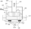
- FIG. 1 shows a film forming atomizer 100 according to the present invention.
- the film forming atomizer 100 spatially connects the raw material container 111 containing the raw material solution 114 and the inside and the outside of the raw material container 111, and the lower end thereof is on the liquid surface of the raw material solution 114 in the raw material container 111.
- a tubular member 113 installed so as not to touch, an ultrasonic generator 120 having one or more ultrasonic generation sources (ultrasonic vibrating plates) 121 for irradiating ultrasonic waves, and an intermediate liquid in which ultrasonic waves are added to a raw material solution 114.
- the raw material container 111 is provided with a carrier gas introduction port 112 for introducing the carrier gas 131.
- the shapes of the raw material container 111 and the tubular member 113 are not particularly limited, but the cylindrical shape allows the air-fuel mixture 133 in which the carrier gas 131 and the mist 132 are mixed to flow smoothly.
- the carrier gas introduction port 112 is preferably provided above the lower end of the tubular member 113 inside the raw material container 111. By doing so, the carrier gas 131 and the mist 132 can be sufficiently mixed.
- the raw material container 111 may be provided with a mechanism for replenishing the raw material solution 114 according to consumption.
- the members constituting the film-forming atomizer are not particularly limited as long as they are materials and structures that are chemically stable with respect to the raw material solution 114 and have sufficient mechanical strength.
- metal or plastic materials for example, metal or plastic materials. , Glass, metal surface coated with plastic material, etc. can be used.
- the ultrasonic generator 120 includes at least an ultrasonic generation source 121. Further, the ultrasonic wave generator 120 can drive the ultrasonic wave generation source 121 by including an oscillator or the like. Further, the liquid tank 122 accommodates an intermediate liquid 123 for propagating the ultrasonic waves irradiated from the ultrasonic wave generation source 121 to the raw material solution 114.
- the ultrasonic wave emitting surface of the ultrasonic wave source 121 has a flat shape, and the irradiation direction may be fixed by inclining this emitting surface, or may be changed by inclining it by the angle adjusting mechanism 121a. You may.
- the ultrasonic wave generation source 121 may be provided with at least one ultrasonic diaphragm, may be a single diaphragm, or may be configured in combination with means for controlling the irradiation direction of ultrasonic waves. You may. Further, the ultrasonic wave generation source 121 may be provided alone or in plurality depending on the desired mist density, the size of the raw material container 111, and the like. The frequency of the ultrasonic waves emitted from the ultrasonic wave generation source 121 is not limited as long as it generates mist 132 having a desired particle size and particle size, but for example, 1.5 MHz to 4.0 MHz may be used. As a result, the raw material solution 114 is mistized into micron-sized droplets suitable for film formation.
- the ultrasonic wave generation source 121 is located on the outside of the liquid tank 122, and the center of the ultrasonic wave generation source 121 is formed by an extension of the inside of the side wall of the raw material container 111 and an extension of the outside of the side wall of the tubular member 113. Install so that it is located between the surface.
- d be the distance between the straight line passing through the center of the ultrasonic wave generation source 121 and parallel to the outer wall of the tubular member 113 and the outer wall of the tubular member 113.
- the distance d is preferably 5 mm or more, and more preferably 10 mm or more. In this way, a higher density mist can be obtained more stably.
- the upper limit of d can be set within a range of less than the distance between the outer wall of the tubular member 113 and the inner wall of the raw material container 111, but can be, for example, 100 mm or less.
- the intermediate liquid 123 contained in the liquid tank 122 is not particularly limited as long as it does not interfere with ultrasonic waves, and for example, water, alcohols, oils, or the like may be used.
- the liquid tank 122 and the like are not particularly limited as long as they are made of a material and structure that are chemically stable with respect to the intermediate liquid 123 and have a certain degree of mechanical strength.
- a metal or plastic material, glass, a material obtained by coating a metal surface with a plastic material, or the like can be used.
- the liquid tank 122 may further include means for detecting and controlling the liquid amount and temperature of the intermediate liquid 123.
- FIG. 2 is a diagram illustrating a mist generating portion of the film forming atomizer according to the present invention, and is in the vicinity of the liquid level of the raw material solution when ultrasonic waves are being irradiated at the dotted frame portion A in FIG. It is an enlarged view which showed the state schematically.
- Let u be the center line of the ultrasonic emission surface of the ultrasonic source 221.
- a liquid column 214p is generated in the raw material solution 214 along the ultrasonic irradiation direction, and at the same time, mist is formed.
- the ultrasonic wave generation source 221 is tilted by the angle adjusting mechanism 221a so that the center line u does not intersect the side wall of the tubular member 213. Further, the center line u and the line c passing through the center of the tubular member 213 may intersect at any point or may be in a twisted position. Further, at this time, it is preferable that the distance D from the center of the ultrasonic source 221 to the surface formed by the extension of the side wall of the raw material container 211 is such that the liquid column 214p is not significantly blocked by the side wall of the raw material container 211.
- the “particles” in the present invention include those that are incorporated into the semiconductor film and integrated with the film and those that adhere to the surface of the semiconductor film as foreign matter, and are observed as particles when the surface of the film is observed. Point to.
- the particle diameter is a value based on the size of the particles measured by a light scattering type particle measuring machine. Particle size is determined by calibrating the instrument with standard particles of multiple sizes. That is, it is a value classified by comparing the measured value when measuring particles with a measuring machine and the measured value when measuring standard particles. Particles on the surface of the semiconductor film can be measured using, for example, a laser scattering type particle counter.
- the present invention further provides a film forming apparatus using the film forming atomizing apparatus described with reference to FIGS. 1 and 2.
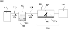
- FIG. 3 is a diagram illustrating one form of the configuration of the film forming apparatus according to the present invention.
- the film forming apparatus 300 according to the present invention has at least an atomizing means 320 for atomizing the raw material solution 321 to form a raw material mist 322 and a film forming device for supplying the mist 322 to the substrate 334 to form a film on the substrate 334.
- the means 330 and the like are provided.
- the film forming apparatus 300 includes the film forming atomizing apparatus 100 of the present invention described with reference to FIGS. 1 and 2 as the atomizing means 320. Further, the carrier gas supply unit 311 and the atomizing means 320 and the film forming means 330 are connected by pipes 313 and 324.
- the carrier gas supply unit 311 may be, for example, an air compressor, various gas cylinders, a nitrogen gas separator, or the like, or may be provided with a mechanism for controlling the gas supply flow rate.
- the pipes 313 and 324 are not particularly limited as long as they have sufficient stability with respect to the temperature in the vicinity of the raw material solution 321 and the film forming means 330, and quartz, polyethylene, polypropylene, vinyl chloride, silicon resin, urethane resin, etc.
- a general resin pipe such as fluororesin can be widely used.
- a pipe that does not pass through the atomizing means 320 may be separately connected to the pipe 324 from the carrier gas supply unit 311 so that the diluted gas can be supplied to the air-fuel mixture 352.
- a plurality of atomizing means 320 may be provided depending on the material to be formed and the like. Further, in this case, the air-fuel mixture 352 supplied from the plurality of atomizing means 320 to the film forming means 330 may be independently supplied to the film forming means 330, in the pipe 324, or in the mixing container ( (Not shown) or the like may be separately provided and mixed.
- the film forming means 330 may include a film forming chamber 331, a susceptor 332 installed in the film forming chamber 331 and holding the substrate 334 forming the film, and a heating means 333 for heating the substrate 334.
- the structure of the film forming chamber 331 is not particularly limited, and for example, a metal such as aluminum or stainless steel may be used, or quartz or silicon carbide may be used when the film is formed at a higher temperature.
- the heating means 333 may be selected according to the material and structure of the substrate 334, the susceptor 332, and the film forming chamber 331. For example, a resistance heating heater or a lamp heater is preferably used.
- the carrier gas 351 is mixed with the mist 322 formed in the atomizing means 320 to form an air-fuel mixture 352, which is conveyed to the film forming means 330 to form a film.
- the film forming apparatus may further include an exhaust means 340.
- the exhaust means 340 may be connected to the film forming means 330 by a pipe or the like, or may be installed with a gap.
- the structure and configuration of the exhaust means 340 are not particularly limited as long as they are made of a material that is stable against heat, gas, and products discharged from the film forming means 330, and a known general exhaust fan or the like. Exhaust pump can be used. Further, depending on the nature of the discharged gas and the product, for example, a mist trap, a wet scrubber, a bag filter, an abatement device and the like may be provided.
- FIG. 3 the form of the film forming means 330 in which the substrate 334 is installed inside the film forming chamber 331 has been described, but the film forming apparatus according to the present invention is not limited to this, and the film forming means 430 is as shown in FIG.
- a film forming apparatus 400 may be used as a film forming apparatus 400 in which the air-fuel mixture 452 is directly sprayed onto the substrate 434 installed on the susceptor 432 using a nozzle 431 that discharges the air-fuel mixture 452 containing the mist 422.
- one or both of the nozzle 431 and the susceptor 432 may be provided with a driving means for driving in the horizontal direction, and the film may be formed while changing the relative positions of the substrate 434 and the nozzle 431 in the horizontal direction.
- the susceptor 432 may be provided with a heating means 433 for heating the substrate 434.
- the film forming means 430 may include an exhaust means 435. The exhaust means 435 may be integrated with the nozzle 431 or may be installed separately. The same items as those in FIGS. 1 to 3 will be omitted as appropriate.
- Example 1 The film formation of ⁇ -gallium oxide was carried out using the film forming atomizer shown in FIGS. 1 and 2 and the film forming apparatus shown in FIG.
- a raw material container made of borosilicate glass and a tubular member were used for the atomizing device for film formation, and a quartz film forming chamber was prepared.
- a gas cylinder filled with nitrogen gas was used to supply the carrier gas.
- the gas cylinder and the film-forming atomizer were connected by a urethane resin tube, and the film-forming atomizer and the film-forming chamber were connected by a quartz pipe.
- a raw material solution 1% by volume of hydrochloric acid having a concentration of 34% was added to an aqueous solution of gallium acetylacetonate 0.02 mol / L, and the mixture was stirred with a stirrer for 60 minutes, and this was filled in a raw material container.
- a device equipped with two ultrasonic diaphragms (frequency 2.4 MHz, irradiation angle 80 °) was used.
- the center of the ultrasonic diaphragm was set at a position 10 mm outward from the side wall of the tubular member, and the ultrasonic diaphragm was installed so that the center line u did not intersect the side wall of the tubular member as shown in FIG.
- a c-plane sapphire substrate with a thickness of 0.6 mm and a diameter of 4 inches (about 10 cm) was placed on a quartz susceptor installed in the film formation chamber and heated so that the substrate temperature became 500 ° C.
- the ultrasonic vibration was propagated to the precursor in the raw material container through water through an ultrasonic diaphragm to atomize (mist) the raw material solution.
- nitrogen gas was added to the raw material container at a flow rate of 5 L / min, and a mixture of mist and nitrogen gas was supplied to the film forming chamber for 60 minutes to perform film formation. Immediately after this, the supply of nitrogen gas was stopped, and the supply of the air-fuel mixture to the film forming chamber was stopped.
- the film thickness of the prepared film was measured by light reflectance analysis, and the growth rate was calculated. Further, the density of particles (diameter 0.5 ⁇ m or more) on the film was evaluated by a substrate inspection machine (KLA candela-CS10).
- Example 2 The film was formed in the same manner as in Example 1 except that the nitrogen gas flow rate was set to 10 L / min.
- Example 3 ⁇ -Gallium oxide was deposited using the same apparatus and raw material solution as in Example 1 except that the film forming apparatus shown in FIG. 4 was used as the film forming apparatus.
- a quartz mist discharge nozzle was used.
- An aluminum hot plate was used as the susceptor, and the substrate was heated to 450 ° C.
- the susceptor was reciprocated in the horizontal direction under the mist discharge nozzle at a speed of 10 mm / s, and 5 L / min of air-fuel mixture was supplied from the mist discharge nozzle to the substrate on the susceptor to form a film for 60 minutes.
- Example 1 A film was formed in the same manner as in Example 1 except that the ultrasonic waves were irradiated toward the side wall of the tubular member.
- Example 2 A film was formed in the same manner as in Example 2 except that the ultrasonic wave was irradiated toward the side wall of the tubular member.
- Table 1 shows the growth rate and the particle density of the obtained film in Examples 1, 2 and 3 and Comparative Examples 1 and 2.
- the film forming apparatus according to the present invention is an excellent one capable of producing a high-quality film having a high growth rate and few particles. You can see that. On the other hand, in Comparative Examples 1 and 2 using the conventional atomizing apparatus for film formation, the growth rate was low and many particles were attached.
- Example 4 The film was formed under the same conditions as in Example 1 except that the film forming time, that is, the time for supplying the mixture of mist and nitrogen gas to the film forming chamber was 120 minutes, to form a semiconductor film having a film thickness of 1 ⁇ m or more.
- the membrane was made. Then, the density of particles (diameter 0.3 ⁇ m or more) on the surface of the film obtained by film formation was evaluated by a substrate inspection machine (KLA candela-CS10).
- Example 5 The film was formed under the same conditions as in Example 2 except that the film formation time was 120 minutes, and the evaluation was performed under the same conditions as in Example 4.
- Example 6 The film was formed under the same conditions as in Example 3 except that the film formation time was 120 minutes, and the evaluation was performed under the same conditions as in Example 4.
- Comparative Example 3 The film was formed under the same conditions as in Comparative Example 1 except that the film formation time was 120 minutes, and the evaluation was performed under the same conditions as in Example 4.
- Comparative Example 4 The film was formed under the same conditions as in Comparative Example 2 except that the film formation time was 120 minutes, and the evaluation was performed under the same conditions as in Example 4.
- Table 2 shows the growth rate and the particle density of the obtained film in Examples 4, 5 and 6 and Comparative Examples 3 and 4.
- the present invention is not limited to the above embodiment.
- the above-described embodiment is an example, and any object having substantially the same configuration as the technical idea described in the claims of the present invention and exhibiting the same effect and effect is the present invention. Is included in the technical scope of.
Landscapes
- Chemical & Material Sciences (AREA)
- Engineering & Computer Science (AREA)
- Microelectronics & Electronic Packaging (AREA)
- Condensed Matter Physics & Semiconductors (AREA)
- Power Engineering (AREA)
- Computer Hardware Design (AREA)
- Manufacturing & Machinery (AREA)
- General Physics & Mathematics (AREA)
- Physics & Mathematics (AREA)
- Materials Engineering (AREA)
- Chemical Kinetics & Catalysis (AREA)
- Metallurgy (AREA)
- Organic Chemistry (AREA)
- Mechanical Engineering (AREA)
- General Chemical & Material Sciences (AREA)
- Inorganic Chemistry (AREA)
- Dispersion Chemistry (AREA)
- Crystallography & Structural Chemistry (AREA)
- Chemical Vapour Deposition (AREA)
- Liquid Deposition Of Substances Of Which Semiconductor Devices Are Composed (AREA)
- Special Spraying Apparatus (AREA)
Abstract
本発明は、原料溶液を収容する原料容器と、前記原料容器の内部と外部を空間的に接続し、且つその下端が前記原料容器内において前記原料溶液の液面に触れないように設置された筒状部材と、超音波を照射する超音波発生源を一つ以上有する超音波発生器と、前記超音波を前記原料溶液に中間液を介して伝播させる液槽とを有する成膜用霧化装置であって、前記超音波発生源は、前記液槽の外側にあり、前記超音波発生源の中心が前記原料容器の側壁の内側の延長がなす面と前記筒状部材の側壁の外側の延長がなす面との間にあり、前記超音波発生源の超音波射出面の中心線をuとしたとき、前記中心線uが前記筒状部材の側壁と交わらないように超音波発生源が設けられている成膜用霧化装置である。これにより、パーティクル付着が抑制された高品質な薄膜を形成可能とする成膜用霧化装置を提供する。
Description
本発明は、成膜用霧化装置およびこれを用いた成膜装置に関する。
霧化されたミスト状の原料を用いて、基板上に薄膜を形成させるミスト化学気相成長法(Mist Chemical Vapor Deposition:Mist CVD。以下、「ミストCVD法」ともいう)が開発され、酸化物半導体膜などの作製に用いられている(特許文献1、2)。ミストCVD法での膜形成では超音波によりミストを得る方式が一般的である。
しかしながら、これまで高品質な膜を形成するための原料霧化手法は確立されておらず、原料ミストの品質に起因したパーティクルが、作製した膜に多数付着する問題があった。また、成膜速度を高める場合などにミスト供給量を増加させると、このようなパーティクル付着がより顕著になることが知られており、膜品質と生産性の両立が課題であった。
本発明は、上記問題を解決するためになされたものであり、パーティクル付着が抑制された高品質な薄膜を効率良く形成可能とする成膜用霧化装置、およびこれを用いて高品質な膜を高い生産性で形成するための成膜装置を提供することを目的とする。
本発明は、上記目的を達成するためになされたものであり、原料溶液を収容する原料容器と、前記原料容器の内部と外部を空間的に接続し、且つその下端が前記原料容器内において前記原料溶液の液面に触れないように設置された筒状部材と、超音波を照射する超音波発生源を一つ以上有する超音波発生器と、前記超音波を前記原料溶液に中間液を介して伝播させる液槽とを有する成膜用霧化装置であって、前記超音波発生源は、前記液槽の外側にあり、前記超音波発生源の中心が前記原料容器の側壁の内側の延長がなす面と前記筒状部材の側壁の外側の延長がなす面との間にあり、前記超音波発生源の超音波射出面の中心線をuとしたとき、前記中心線uが前記筒状部材の側壁と交わらないように超音波発生源が設けられている成膜用霧化装置を提供する。
このような成膜用霧化装置であれば、成膜に適した、高品質で良好な高密度ミストを安定して得ることができるものとなるため、パーティクルの少ない高品質な膜を効率良く形成可能な成膜用霧化装置となる。
このとき、前記超音波発生源の中心を通り、前記筒状部材の外壁と平行な直線と前記筒状部材の外壁との距離dが、5mm以上となるように超音波発生源が設けられていることが好ましい。
このようにすれば、より高密度のミストをより安定して得ることができるものとなる。
また、原料溶液を霧化して原料ミストを形成する霧化手段と、前記ミストを基体に供給して前記基体上に膜を形成する成膜手段とを少なくとも具備する成膜装置であって、前記霧化手段として上記の成膜用霧化装置を具備する成膜装置を提供する。
このような装置とすれば、高品質な膜を高い生産性で製造することができるものとなる。
以上のように、本発明によれば、高品質で高密度なミストが安定して得られる成膜用霧化装置を提供できる。また、本発明によれば、高い生産性で高品質な膜を製造可能な成膜装置を提供できる。
以下、本発明を詳細に説明するが、本発明はこれらに限定されるものではない。
上述のように、パーティクル付着が抑制された高品質な薄膜を形成可能とする成膜用霧化装置、およびこれを用いて高品質な膜を高い生産性で形成するための成膜装置が求められていた。
本発明者らは、上記課題について鋭意検討を重ねた結果、原料溶液を収容する原料容器と、前記原料容器の内部と外部を空間的に接続し、且つその下端が前記原料容器内において前記原料溶液の液面に触れないように設置された筒状部材と、超音波を照射する超音波発生源を一つ以上有する超音波発生器と、前記超音波を前記原料溶液に中間液を介して伝播させる液槽とを有する成膜用霧化装置であって、前記超音波発生源は、前記液槽の外側にあり、前記超音波発生源の中心が前記原料容器の側壁の内側の延長がなす面と前記筒状部材の側壁の外側の延長がなす面との間にあり、前記超音波発生源の超音波射出面の中心線をuとしたとき、前記中心線uが前記筒状部材の側壁と交わらないように超音波発生源が設けられている成膜用霧化装置により、パーティクル付着が抑制された高品質な薄膜を高い生産性で形成できるものとなることを見出し、本発明を完成した。
以下、図面を参照して説明する。
(成膜用霧化装置)
図1に、本発明に係る成膜用霧化装置100を示す。成膜用霧化装置100は、原料溶液114を収容する原料容器111と、原料容器111の内部と外部を空間的に接続し、且つその下端が原料容器111内において原料溶液114の液面に触れないように設置された筒状部材113と、超音波を照射する超音波発生源(超音波振動板)121を一つ以上有する超音波発生器120と、超音波を原料溶液114に中間液123を介して伝播させる液槽122とを具備する。
図1に、本発明に係る成膜用霧化装置100を示す。成膜用霧化装置100は、原料溶液114を収容する原料容器111と、原料容器111の内部と外部を空間的に接続し、且つその下端が原料容器111内において原料溶液114の液面に触れないように設置された筒状部材113と、超音波を照射する超音波発生源(超音波振動板)121を一つ以上有する超音波発生器120と、超音波を原料溶液114に中間液123を介して伝播させる液槽122とを具備する。
原料容器111にはキャリアガス131を導入するためのキャリアガス導入口112が設置されている。原料容器111および筒状部材113の形状は特に限定されないが、円柱状とすることでキャリアガス131とミスト132が混合した混合気133を円滑に流すことができる。キャリアガス導入口112は筒状部材113の原料容器111内部における下端よりも上方に設けられることが好ましい。このようにすることで、キャリアガス131とミスト132を十分に混合することができる。また原料容器111は、図には示していないが、原料溶液114の消費に応じて補充する機構を備えていても良い。
成膜用霧化装置を構成する部材は、原料溶液114に対して化学的に安定かつ十分な機械的強度をもつ材質および構造であれば特に限定されるものではなく、例えば、金属やプラスチック材料、ガラス、金属表面にプラスチック材料をコーティングした材料等が利用できる。
超音波発生器120は、少なくとも、超音波発生源121を備えている。また、超音波発生器120は発振器等を備えることで、超音波発生源121を駆動させることができる。また、液槽122は、超音波発生源121から照射された超音波を原料溶液114に伝播するための中間液123を収容するものである。超音波発生源121の超音波の射出面は平坦な形状をしており、照射方向はこの射出面を傾斜させて固定しても良いし、角度調節機構121aにより傾斜させることで変えられるようにしても良い。また、超音波発生源121は、少なくとも1つの超音波振動板を備えていればよく、振動板単体であっても良いし、超音波の照射方向を制御するための手段と組み合わせて構成されていても良い。また、超音波発生源121は、所望のミスト密度や原料容器111のサイズなどに応じて単一または複数設けて良い。超音波発生源121から照射される超音波の周波数は、所望の粒径と粒度のミスト132を発生するものであれば限定されないが、例えば、1.5MHzから4.0MHzを用いると良い。これにより原料溶液114が成膜に適したミクロンサイズの液滴にミスト化される。
また、超音波発生源121は、液槽122の外側にあり、超音波発生源121の中心が原料容器111の側壁の内側の延長がなす面と筒状部材113の側壁の外側の延長がなす面との間に位置するように設置する。このとき、超音波発生源121の中心を通り、筒状部材113の外壁と平行な直線と、筒状部材113の外壁との距離をdとする。距離dは5mm以上とするのが好ましく、10mm以上とするのがより好ましい。このようにすれば、より高密度のミストをより安定して得ることができるものとなる。なお、dの上限値は、筒状部材113の外壁と原料容器111の内壁との距離未満の範囲で定めることができるが、例えば、100mm以下とすることができる。
液槽122に収容されている中間液123は、超音波を阻害しなければ特に限定されず、例えば、水やアルコール類およびオイル類などを用いて良い。液槽122等は、中間液123に対して化学的に安定で、ある程度の機械的強度をもつ材質および構造であれば特に限定されるものではない。例えば、金属やプラスチック材料、ガラス、金属表面にプラスチック材料をコーティングした材料等が利用できる。また液槽122は、図には示していないが、中間液123の液量や温度を検知および制御する手段をさらに備えていても良い。
図2は、本発明に係る成膜用霧化装置のミスト発生部を説明する図であり、図1の点線枠箇所Aにおいて、超音波を照射しているときの原料溶液の液面近傍における状態を模式的に示した拡大図である。超音波発生源221の超音波射出面の中心線をuとする。超音波発生源221から原料溶液214の下方より中心線u方向に超音波が照射されると、原料溶液214には超音波照射方向に沿って液柱214pが生じ、同時にミスト化される。
このとき、中心線uは筒状部材213の側壁と交わらないように角度調節機構221aにより超音波発生源221を傾ける。また中心線uと筒状部材213の中心を通る線cは任意の点で交わっても良いし、ねじれの位置にあっても良い。また、このとき、超音波発生源221の中心から原料容器211の側壁の延長がなす面までの距離Dは、液柱214pが原料容器211の側壁に著しく遮られない程度とすることが好ましい。これにより混合気の流れが阻害されずに成膜用霧化装置外部へ供給されるようになり、より効率的な成膜が可能となる。また、同時に、未反応生成物やパーティクルの原因となる比較的大きな粒径の液滴が混合気に混入することが抑制されるので、より高品質な膜の形成が可能になる。尚、図1と同じものについては適宜説明を省略する。
なお、本発明における「パーティクル」とは、半導体膜中に取り込まれ膜と一体化したもの及び半導体膜表面に異物として付着したものを含み、膜の表面を観察したときにパーティクルとして観察されるものを指す。また、パーティクルの直径は、光散乱式のパーティクル測定機により測定されたパーティクルのサイズに基づく値である。パーティクルのサイズは、測定機を複数のサイズの標準粒子で校正することで判定される。即ち、測定機でパーティクルを測定した際の測定値と標準粒子を測定した際の測定値を照らし合わせることにより分類される値である。半導体膜の表面におけるパーティクルは、例えばレーザー散乱式のパーティクルカウンタを用いて測定することができる。
(成膜装置)
本発明は、さらに図1および図2で説明した成膜用霧化装置を用いた成膜装置を提供する。
本発明は、さらに図1および図2で説明した成膜用霧化装置を用いた成膜装置を提供する。
図3は、本発明に係る成膜装置の構成の一形態を説明する図である。本発明に係る成膜装置300は、少なくとも、原料溶液321を霧化して原料ミスト322を形成する霧化手段320と、ミスト322を基体334に供給して基体334上に膜を形成する成膜手段330とを具備する。成膜装置300は、霧化手段320として、図1および図2で説明した本発明の成膜用霧化装置100を備えている。さらに、キャリアガス供給部311や、霧化手段320と成膜手段330は配管313、324で接続されている。
キャリアガス供給部311は、例えば、空気圧縮機や各種ガスボンベまたは窒素ガス分離機などでもよく、また、ガスの供給流量を制御する機構を備えていて良い。
配管313、324は原料溶液321や成膜手段330付近における温度などに対して十分な安定性を持つものであれば特に限定されず、石英やポリエチレン、ポリプロピレン、塩化ビニル、シリコン樹脂、ウレタン樹脂、フッ素樹脂などといった一般的な樹脂製の配管を広く用いることができる。
また、図には示していないが、キャリアガス供給部311から霧化手段320を介さない配管を別途配管324に接続し、混合気352に希釈ガスを供給できるようにしても良い。
霧化手段320は、成膜する材料などに応じて複数台を備えていても良い。またこの場合、複数の霧化手段320から成膜手段330へ供給される混合気352は、それぞれ独立して成膜手段330に供給されても良いし、配管324中、あるいは混合用の容器(不図示)などを別途設けて混合しても良い。
成膜手段330は、成膜室331と、成膜室331内に設置され、膜を形成する基体334を保持するサセプター332と、基体334を加熱する加熱手段333を備えていて良い。
成膜室331の構造等は特に限定されるものではなく、例えば、アルミニウムやステンレスなどの金属を用いて良いし、より高温で成膜を行う場合には石英や炭化シリコンを用いても良い。
加熱手段333は基体334、サセプター332および成膜室331の材質や構造によって選定されればよく、例えば、抵抗加熱ヒーターやランプヒーターが好適に用いられる。
キャリアガス351は、霧化手段320内で形成されたミスト322と混合されて混合気352となり、成膜手段330へと搬送されて成膜が行われる。
また本発明に係る成膜装置は、さらに排気手段340を備えていて良い。排気手段340は成膜手段330に配管などで接続されていても良いし、間隙を置いて設置されていても良い。また排気手段340は成膜手段330から排出される熱およびガスや生成物に対して安定な素材で構成されてさえいれば、特に構造や構成は限定されず、公知の一般的な排気ファンや排気ポンプが使用できる。また排出されるガスや生成物の性質に応じて、例えば、ミストトラップ、ウェットスクラバー、バグフィルター、除害装置などを備えていても良い。
図3では、基体334が成膜室331内部に設置される成膜手段330の形態を説明したが、本発明に係る成膜装置ではこれに限らず、図4に示すように成膜手段430として、ミスト422を含む混合気452を吐出するノズル431を用い、サセプター432の上に設置された基体434へ混合気452を直接吹き付けて成膜する成膜装置400としても良い。
この場合、ノズル431とサセプター432のうち、いずれかまたは両方が水平方向に駆動する駆動手段を備え、基体434とノズル431の水平方向における相対位置を変化させながら成膜が行われて良い。またサセプター432は基板434を加熱する加熱手段433を備えていて良い。また成膜手段430は、排気手段435を備えていて良い。排気手段435はノズル431と一体化していても良いし、別々に設置されていても良い。尚、図1から3と同じものについては適宜説明を省略する。
以下、実施例を挙げて本発明について詳細に説明するが、これは本発明を限定するものではない。
(実施例1)
図1および図2に示した成膜用霧化装置と、図3に示した成膜装置を用いて、α-酸化ガリウムの成膜を行った。
図1および図2に示した成膜用霧化装置と、図3に示した成膜装置を用いて、α-酸化ガリウムの成膜を行った。
成膜用霧化装置にはいずれも硼珪酸ガラス製の原料容器と筒状部材を使用し、また、石英製の成膜室を用意した。キャリアガス供給には窒素ガスが充填されたガスボンベを使用した。ガスボンベと成膜用霧化装置をウレタン樹脂製チューブで接続し、さらに成膜用霧化装置と成膜室を石英製の配管で接続した。
原料溶液として、ガリウムアセチルアセトナート0.02mol/Lの水溶液に濃度34%の塩酸を体積比で1%加え、スターラーで60分間攪拌したものを用意し、これを原料容器に充填した。成膜用霧化装置は2基の超音波振動板(周波数2.4MHz、照射角度80°)を備えたものを使用した。超音波振動板の中心を筒状部材の側壁から外側に10mm離れた位置とし、図2のように、中心線uが筒状部材の側壁と交わらないように超音波振動板を設置した。
次に、厚さ0.6mm、直径4インチ(約10cm)のc面サファイア基板を、成膜室内に設置した石英製のサセプターに載置し、基板温度が500℃になるように加熱した。
次に、超音波振動板により水を通じて原料容器内の前駆体に超音波振動を伝播させて、原料溶液を霧化(ミスト化)した。
次に、原料容器に窒素ガスを5L/minの流量で加え、成膜室にミストと窒素ガスの混合気を60分間供給して成膜を行った。この直後、窒素ガスの供給を停止し、成膜室への混合気供給を停止した。
作製した積層体の結晶層は、X線回折測定で2θ=40.3°にピークが現れたことから、α相のGa2O3であることが確認された。
この後、作製した膜の膜厚を光反射率解析で測定し、成長速度を算出した。また、膜上のパーティクル(直径0.5μm以上)密度を基板検査機(KLA candela-CS10)で評価した。
(実施例2)
窒素ガス流量を10L/minとした以外は実施例1と同様に成膜を行った。
窒素ガス流量を10L/minとした以外は実施例1と同様に成膜を行った。
作製した積層体の結晶層は、X線回折測定で2θ=40.3°にピークが現れたことから、α相のGa2O3であることが確認された。
この後、実施例1と同様に膜を評価した。
(実施例3)
成膜装置に図4で示した成膜装置を用いた他は、実施例1と同様の装置および原料溶液を使用してα-酸化ガリウムの成膜を行った。ミスト吐出ノズルには石英製のものを使用した。サセプターにはアルミ製ホットプレートを使用し、基板を450℃に加熱した。次にサセプターを10mm/sの速度でミスト吐出ノズルの下を水平方向に往復駆動させ、さらにミスト吐出ノズルからサセプター上の基板へ混合気を5L/min供給して60分間成膜を行った。
成膜装置に図4で示した成膜装置を用いた他は、実施例1と同様の装置および原料溶液を使用してα-酸化ガリウムの成膜を行った。ミスト吐出ノズルには石英製のものを使用した。サセプターにはアルミ製ホットプレートを使用し、基板を450℃に加熱した。次にサセプターを10mm/sの速度でミスト吐出ノズルの下を水平方向に往復駆動させ、さらにミスト吐出ノズルからサセプター上の基板へ混合気を5L/min供給して60分間成膜を行った。
作製した積層体の結晶層は、X線回折測定で2θ=40.3°にピークが現れたことから、α相のGa2O3であることが確認された。この後、実施例1と同様に膜を評価した。
(比較例1)
超音波を、筒状部材の側壁に向けて照射した他は、実施例1と同様に成膜を行った。
超音波を、筒状部材の側壁に向けて照射した他は、実施例1と同様に成膜を行った。
作製した積層体の結晶層は、X線回折測定で2θ=40.3°にピークが現れたことから、α相のGa2O3であることが確認された。この後、実施例1と同様に膜を評価した。
(比較例2)
超音波を、筒状部材の側壁に向けて照射した他は、実施例2と同様に成膜を行った。
超音波を、筒状部材の側壁に向けて照射した他は、実施例2と同様に成膜を行った。
作製した積層体の結晶層は、X線回折測定で2θ=40.3°にピークが現れたことから、α相のGa2O3であることが確認された。この後、実施例1と同様に膜を評価した。
実施例1、2、3及び比較例1、2における成長速度および得られた膜のパーティクル密度を表1に示す。

表1より、実施例1、2、3に示されるように、本発明に係る成膜装置は、高い成長速度で、かつパーティクルが少ない高品質な膜を作製することのできる優れたものであることが分かる。一方、従来技術の成膜用霧化装置を用いた比較例1、2では、成長速度が低く、また多くのパーティクルが付着していた。
(実施例4)
成膜時間、すなわち、成膜室にミストと窒素ガスの混合気を供給する時間を120分間としたこと以外は実施例1と同じ条件で成膜を行い、膜厚1μm以上の半導体膜の成膜を行った。そして、成膜して得た膜の表面のパーティクル(直径0.3μm以上)密度を、基板検査機(KLA candela-CS10)で評価した。
成膜時間、すなわち、成膜室にミストと窒素ガスの混合気を供給する時間を120分間としたこと以外は実施例1と同じ条件で成膜を行い、膜厚1μm以上の半導体膜の成膜を行った。そして、成膜して得た膜の表面のパーティクル(直径0.3μm以上)密度を、基板検査機(KLA candela-CS10)で評価した。
(実施例5)
成膜時間を120分間としたこと以外は実施例2と同条件で成膜し、実施例4と同条件で評価を行った。
成膜時間を120分間としたこと以外は実施例2と同条件で成膜し、実施例4と同条件で評価を行った。
(実施例6)
成膜時間を120分間としたこと以外は実施例3と同条件で成膜し、実施例4と同条件で評価を行った。
成膜時間を120分間としたこと以外は実施例3と同条件で成膜し、実施例4と同条件で評価を行った。
(比較例3)
成膜時間を120分間としたこと以外は比較例1と同条件で成膜し、実施例4と同条件で評価を行った。
成膜時間を120分間としたこと以外は比較例1と同条件で成膜し、実施例4と同条件で評価を行った。
(比較例4)
成膜時間を120分間としたこと以外は比較例2と同条件で成膜し、実施例4と同条件で評価を行った。
成膜時間を120分間としたこと以外は比較例2と同条件で成膜し、実施例4と同条件で評価を行った。
実施例4、5、6及び比較例3、4における成長速度および得られた膜のパーティクル密度を表2に示す。

表2より、実施例4、5、6に示されるように、本発明に係る成膜装置を用いて成膜を行った場合、高い成長速度で、かつパーティクルが少ない高品質な膜を作製することができることが分かる。特に、直径0.3μm以上のパーティクル密度が50個/cm2以下である半導体膜を得ることができた。一方、従来技術の成膜用霧化装置を用いた比較例3、4では、成長速度が低く、また多くのパーティクルが付着していた。
なお、本発明は、上記実施形態に限定されるものではない。上記実施形態は例示であり、本発明の特許請求の範囲に記載された技術的思想と実質的に同一な構成を有し、同様な作用効果を奏するものは、いかなるものであっても本発明の技術的範囲に包含される。
Claims (3)
- 原料溶液を収容する原料容器と、前記原料容器の内部と外部を空間的に接続し、且つその下端が前記原料容器内において前記原料溶液の液面に触れないように設置された筒状部材と、超音波を照射する超音波発生源を一つ以上有する超音波発生器と、前記超音波を前記原料溶液に中間液を介して伝播させる液槽とを有する成膜用霧化装置であって、
前記超音波発生源は、前記液槽の外側にあり、
前記超音波発生源の中心が前記原料容器の側壁の内側の延長がなす面と前記筒状部材の側壁の外側の延長がなす面との間にあり、
前記超音波発生源の超音波射出面の中心線をuとしたとき、前記中心線uが前記筒状部材の側壁と交わらないように超音波発生源が設けられていることを特徴とする成膜用霧化装置。 - 前記超音波発生源の中心を通り、前記筒状部材の外壁と平行な直線と前記筒状部材の外壁との距離dが、5mm以上となるように超音波発生源が設けられていることを特徴とする請求項1に記載の成膜用霧化装置。
- 原料溶液を霧化して原料ミストを形成する霧化手段と、前記ミストを基体に供給して前記基体上に膜を形成する成膜手段とを少なくとも具備する成膜装置であって、
前記霧化手段が請求項1又は請求項2に記載の霧化装置であることを特徴とする成膜装置。
Priority Applications (4)
| Application Number | Priority Date | Filing Date | Title |
|---|---|---|---|
| EP21760747.2A EP4112185A4 (en) | 2020-02-27 | 2021-02-18 | ATOMIZING DEVICE FOR FILM FORMATION AND FILM FORMATION DEVICE USING SAME |
| KR1020227029172A KR20220143046A (ko) | 2020-02-27 | 2021-02-18 | 성막용 무화장치 및 이것을 이용한 성막장치 |
| US17/801,485 US20220410199A1 (en) | 2020-02-27 | 2021-02-18 | Atomizing apparatus for film formation and film forming apparatus using the same |
| CN202180016328.0A CN115175769A (zh) | 2020-02-27 | 2021-02-18 | 成膜用雾化装置及使用了该成膜用雾化装置的成膜装置 |
Applications Claiming Priority (2)
| Application Number | Priority Date | Filing Date | Title |
|---|---|---|---|
| JP2020032307 | 2020-02-27 | ||
| JP2020-032307 | 2020-02-27 |
Publications (1)
| Publication Number | Publication Date |
|---|---|
| WO2021172154A1 true WO2021172154A1 (ja) | 2021-09-02 |
Family
ID=77491513
Family Applications (1)
| Application Number | Title | Priority Date | Filing Date |
|---|---|---|---|
| PCT/JP2021/006048 WO2021172154A1 (ja) | 2020-02-27 | 2021-02-18 | 成膜用霧化装置およびこれを用いた成膜装置 |
Country Status (7)
| Country | Link |
|---|---|
| US (1) | US20220410199A1 (ja) |
| EP (1) | EP4112185A4 (ja) |
| JP (1) | JP6975417B2 (ja) |
| KR (1) | KR20220143046A (ja) |
| CN (1) | CN115175769A (ja) |
| TW (1) | TW202209502A (ja) |
| WO (1) | WO2021172154A1 (ja) |
Families Citing this family (2)
| Publication number | Priority date | Publication date | Assignee | Title |
|---|---|---|---|---|
| JP6994694B2 (ja) * | 2020-02-27 | 2022-01-14 | 信越化学工業株式会社 | 成膜用霧化装置及びこれを用いた成膜装置 |
| CN117912931A (zh) * | 2024-03-19 | 2024-04-19 | 宁波华仪宁创智能科技有限公司 | 非接触样品雾化进样装置和方法 |
Citations (10)
| Publication number | Priority date | Publication date | Assignee | Title |
|---|---|---|---|---|
| JPH10140356A (ja) * | 1996-11-12 | 1998-05-26 | Matsushita Electric Ind Co Ltd | 気化装置及びcvd装置 |
| JP2005305233A (ja) * | 2004-04-19 | 2005-11-04 | Shizuo Fujita | 成膜用霧化装置 |
| JP2013028480A (ja) | 2011-07-27 | 2013-02-07 | Kochi Univ Of Technology | ドーパントを添加した結晶性の高い導電性α型酸化ガリウム薄膜およびその生成方法 |
| JP2014063973A (ja) | 2012-08-26 | 2014-04-10 | Kumamoto Univ | 酸化亜鉛結晶層の製造方法及び酸化亜鉛結晶層並びにミスト化学気相成長装置 |
| WO2015019468A1 (ja) * | 2013-08-08 | 2015-02-12 | 東芝三菱電機産業システム株式会社 | 霧化装置 |
| JP2016187764A (ja) * | 2015-03-30 | 2016-11-04 | 本多電子株式会社 | 超音波霧化装置 |
| JP2018070422A (ja) * | 2016-11-01 | 2018-05-10 | 国立大学法人 和歌山大学 | 酸化ガリウムの製造方法及び結晶成長装置 |
| JP2018142637A (ja) * | 2017-02-28 | 2018-09-13 | 株式会社Flosfia | 処理方法 |
| JP2020188170A (ja) * | 2019-05-15 | 2020-11-19 | トヨタ自動車株式会社 | ミスト生成装置及び成膜装置 |
| JP2020196930A (ja) * | 2019-06-03 | 2020-12-10 | トヨタ自動車株式会社 | ミスト生成装置、成膜装置、及び成膜装置を用いた成膜方法 |
Family Cites Families (4)
| Publication number | Priority date | Publication date | Assignee | Title |
|---|---|---|---|---|
| JP4990707B2 (ja) * | 2007-07-24 | 2012-08-01 | パナソニック株式会社 | 超音波霧発生装置 |
| JP5470514B2 (ja) * | 2009-12-22 | 2014-04-16 | ナノミストテクノロジーズ株式会社 | 超音波霧化方法と霧化装置 |
| KR102151325B1 (ko) * | 2015-12-11 | 2020-09-02 | 도시바 미쓰비시덴키 산교시스템 가부시키가이샤 | 미스트 도포 성막 장치 및 미스트 도포 성막 방법 |
| JP6760709B2 (ja) * | 2017-05-31 | 2020-09-23 | 東芝三菱電機産業システム株式会社 | ミスト塗布成膜装置の塗布ヘッドおよびそのメンテナンス方法 |
-
2021
- 2021-02-04 JP JP2021016942A patent/JP6975417B2/ja active Active
- 2021-02-18 CN CN202180016328.0A patent/CN115175769A/zh active Pending
- 2021-02-18 US US17/801,485 patent/US20220410199A1/en active Pending
- 2021-02-18 EP EP21760747.2A patent/EP4112185A4/en active Pending
- 2021-02-18 WO PCT/JP2021/006048 patent/WO2021172154A1/ja unknown
- 2021-02-18 KR KR1020227029172A patent/KR20220143046A/ko unknown
- 2021-02-23 TW TW110106245A patent/TW202209502A/zh unknown
Patent Citations (10)
| Publication number | Priority date | Publication date | Assignee | Title |
|---|---|---|---|---|
| JPH10140356A (ja) * | 1996-11-12 | 1998-05-26 | Matsushita Electric Ind Co Ltd | 気化装置及びcvd装置 |
| JP2005305233A (ja) * | 2004-04-19 | 2005-11-04 | Shizuo Fujita | 成膜用霧化装置 |
| JP2013028480A (ja) | 2011-07-27 | 2013-02-07 | Kochi Univ Of Technology | ドーパントを添加した結晶性の高い導電性α型酸化ガリウム薄膜およびその生成方法 |
| JP2014063973A (ja) | 2012-08-26 | 2014-04-10 | Kumamoto Univ | 酸化亜鉛結晶層の製造方法及び酸化亜鉛結晶層並びにミスト化学気相成長装置 |
| WO2015019468A1 (ja) * | 2013-08-08 | 2015-02-12 | 東芝三菱電機産業システム株式会社 | 霧化装置 |
| JP2016187764A (ja) * | 2015-03-30 | 2016-11-04 | 本多電子株式会社 | 超音波霧化装置 |
| JP2018070422A (ja) * | 2016-11-01 | 2018-05-10 | 国立大学法人 和歌山大学 | 酸化ガリウムの製造方法及び結晶成長装置 |
| JP2018142637A (ja) * | 2017-02-28 | 2018-09-13 | 株式会社Flosfia | 処理方法 |
| JP2020188170A (ja) * | 2019-05-15 | 2020-11-19 | トヨタ自動車株式会社 | ミスト生成装置及び成膜装置 |
| JP2020196930A (ja) * | 2019-06-03 | 2020-12-10 | トヨタ自動車株式会社 | ミスト生成装置、成膜装置、及び成膜装置を用いた成膜方法 |
Non-Patent Citations (1)
| Title |
|---|
| See also references of EP4112185A4 |
Also Published As
| Publication number | Publication date |
|---|---|
| TW202209502A (zh) | 2022-03-01 |
| KR20220143046A (ko) | 2022-10-24 |
| EP4112185A1 (en) | 2023-01-04 |
| EP4112185A4 (en) | 2024-04-10 |
| JP2021133363A (ja) | 2021-09-13 |
| JP6975417B2 (ja) | 2021-12-01 |
| US20220410199A1 (en) | 2022-12-29 |
| CN115175769A (zh) | 2022-10-11 |
Similar Documents
| Publication | Publication Date | Title |
|---|---|---|
| WO2021172154A1 (ja) | 成膜用霧化装置およびこれを用いた成膜装置 | |
| JP7357301B2 (ja) | 半導体膜及び半導体膜の製造方法 | |
| US6193936B1 (en) | Reactant delivery apparatuses | |
| JP5124760B2 (ja) | 成膜方法及び成膜装置 | |
| CN105986246A (zh) | 成膜装置和成膜方法 | |
| JP2005305233A (ja) | 成膜用霧化装置 | |
| JP2006200013A (ja) | 成膜方法及び成膜装置 | |
| US20060222779A1 (en) | Glow discharge-generated chemical vapor deposition | |
| WO2022030187A1 (ja) | 製膜用霧化装置、製膜装置及び製膜方法 | |
| CN108046612A (zh) | 一种制备镀膜玻璃的方法及装置 | |
| US20240124973A1 (en) | Method for forming film, film-forming apparatus, and laminate | |
| WO2023210381A1 (ja) | 成膜方法、成膜装置、及び積層体 | |
| WO2023132174A1 (ja) | 成膜装置および成膜方法 | |
| JPH07126852A (ja) | ネブライザー式cvd装置 |
Legal Events
| Date | Code | Title | Description |
|---|---|---|---|
| 121 | Ep: the epo has been informed by wipo that ep was designated in this application |
Ref document number: 21760747 Country of ref document: EP Kind code of ref document: A1 |
|
| NENP | Non-entry into the national phase |
Ref country code: DE |
|
| ENP | Entry into the national phase |
Ref document number: 2021760747 Country of ref document: EP Effective date: 20220927 |