WO2021171736A1 - 固体電池の製造方法及び固体電池 - Google Patents
固体電池の製造方法及び固体電池 Download PDFInfo
- Publication number
- WO2021171736A1 WO2021171736A1 PCT/JP2020/046115 JP2020046115W WO2021171736A1 WO 2021171736 A1 WO2021171736 A1 WO 2021171736A1 JP 2020046115 W JP2020046115 W JP 2020046115W WO 2021171736 A1 WO2021171736 A1 WO 2021171736A1
- Authority
- WO
- WIPO (PCT)
- Prior art keywords
- layer
- electrode layer
- electrode
- solid
- state battery
- Prior art date
Links
Images


Classifications
-
- H—ELECTRICITY
- H01—ELECTRIC ELEMENTS
- H01M—PROCESSES OR MEANS, e.g. BATTERIES, FOR THE DIRECT CONVERSION OF CHEMICAL ENERGY INTO ELECTRICAL ENERGY
- H01M10/00—Secondary cells; Manufacture thereof
- H01M10/05—Accumulators with non-aqueous electrolyte
- H01M10/056—Accumulators with non-aqueous electrolyte characterised by the materials used as electrolytes, e.g. mixed inorganic/organic electrolytes
- H01M10/0561—Accumulators with non-aqueous electrolyte characterised by the materials used as electrolytes, e.g. mixed inorganic/organic electrolytes the electrolyte being constituted of inorganic materials only
- H01M10/0562—Solid materials
-
- H—ELECTRICITY
- H01—ELECTRIC ELEMENTS
- H01M—PROCESSES OR MEANS, e.g. BATTERIES, FOR THE DIRECT CONVERSION OF CHEMICAL ENERGY INTO ELECTRICAL ENERGY
- H01M10/00—Secondary cells; Manufacture thereof
- H01M10/05—Accumulators with non-aqueous electrolyte
- H01M10/052—Li-accumulators
- H01M10/0525—Rocking-chair batteries, i.e. batteries with lithium insertion or intercalation in both electrodes; Lithium-ion batteries
-
- H—ELECTRICITY
- H01—ELECTRIC ELEMENTS
- H01M—PROCESSES OR MEANS, e.g. BATTERIES, FOR THE DIRECT CONVERSION OF CHEMICAL ENERGY INTO ELECTRICAL ENERGY
- H01M10/00—Secondary cells; Manufacture thereof
- H01M10/05—Accumulators with non-aqueous electrolyte
- H01M10/058—Construction or manufacture
- H01M10/0585—Construction or manufacture of accumulators having only flat construction elements, i.e. flat positive electrodes, flat negative electrodes and flat separators
-
- H—ELECTRICITY
- H01—ELECTRIC ELEMENTS
- H01M—PROCESSES OR MEANS, e.g. BATTERIES, FOR THE DIRECT CONVERSION OF CHEMICAL ENERGY INTO ELECTRICAL ENERGY
- H01M4/00—Electrodes
- H01M4/02—Electrodes composed of, or comprising, active material
- H01M4/04—Processes of manufacture in general
-
- H—ELECTRICITY
- H01—ELECTRIC ELEMENTS
- H01M—PROCESSES OR MEANS, e.g. BATTERIES, FOR THE DIRECT CONVERSION OF CHEMICAL ENERGY INTO ELECTRICAL ENERGY
- H01M4/00—Electrodes
- H01M4/02—Electrodes composed of, or comprising, active material
- H01M4/13—Electrodes for accumulators with non-aqueous electrolyte, e.g. for lithium-accumulators; Processes of manufacture thereof
-
- H—ELECTRICITY
- H01—ELECTRIC ELEMENTS
- H01M—PROCESSES OR MEANS, e.g. BATTERIES, FOR THE DIRECT CONVERSION OF CHEMICAL ENERGY INTO ELECTRICAL ENERGY
- H01M4/00—Electrodes
- H01M4/02—Electrodes composed of, or comprising, active material
- H01M4/04—Processes of manufacture in general
- H01M4/0402—Methods of deposition of the material
- H01M4/0414—Methods of deposition of the material by screen printing
-
- H—ELECTRICITY
- H01—ELECTRIC ELEMENTS
- H01M—PROCESSES OR MEANS, e.g. BATTERIES, FOR THE DIRECT CONVERSION OF CHEMICAL ENERGY INTO ELECTRICAL ENERGY
- H01M4/00—Electrodes
- H01M4/02—Electrodes composed of, or comprising, active material
- H01M4/13—Electrodes for accumulators with non-aqueous electrolyte, e.g. for lithium-accumulators; Processes of manufacture thereof
- H01M4/139—Processes of manufacture
-
- Y—GENERAL TAGGING OF NEW TECHNOLOGICAL DEVELOPMENTS; GENERAL TAGGING OF CROSS-SECTIONAL TECHNOLOGIES SPANNING OVER SEVERAL SECTIONS OF THE IPC; TECHNICAL SUBJECTS COVERED BY FORMER USPC CROSS-REFERENCE ART COLLECTIONS [XRACs] AND DIGESTS
- Y02—TECHNOLOGIES OR APPLICATIONS FOR MITIGATION OR ADAPTATION AGAINST CLIMATE CHANGE
- Y02E—REDUCTION OF GREENHOUSE GAS [GHG] EMISSIONS, RELATED TO ENERGY GENERATION, TRANSMISSION OR DISTRIBUTION
- Y02E60/00—Enabling technologies; Technologies with a potential or indirect contribution to GHG emissions mitigation
- Y02E60/10—Energy storage using batteries
-
- Y—GENERAL TAGGING OF NEW TECHNOLOGICAL DEVELOPMENTS; GENERAL TAGGING OF CROSS-SECTIONAL TECHNOLOGIES SPANNING OVER SEVERAL SECTIONS OF THE IPC; TECHNICAL SUBJECTS COVERED BY FORMER USPC CROSS-REFERENCE ART COLLECTIONS [XRACs] AND DIGESTS
- Y02—TECHNOLOGIES OR APPLICATIONS FOR MITIGATION OR ADAPTATION AGAINST CLIMATE CHANGE
- Y02P—CLIMATE CHANGE MITIGATION TECHNOLOGIES IN THE PRODUCTION OR PROCESSING OF GOODS
- Y02P70/00—Climate change mitigation technologies in the production process for final industrial or consumer products
- Y02P70/50—Manufacturing or production processes characterised by the final manufactured product
Definitions
- the present invention relates to a method for manufacturing a solid-state battery and a solid-state battery.
- a solid-state battery including a structure in which an electrolyte layer is provided between a pair of electrodes of a positive electrode and a negative electrode is known.
- the electrode and the electrolyte layer are pressurized by covering one or both ends of them with an insulating material, and the ends are deformed or dropped, and the electrolyte layer is formed.
- Patent Document 2 describes a technique for suppressing breakage and film breakage of a laminate cell by a hydrostatic pressure pressing method by continuously increasing the thickness of an electrode from an end to the center.
- the electrodes are subjected to misalignment of the electrode pair sandwiching the electrolyte layer, deformation during thermal crimping, poor crimping, deformation during firing, etc. in the manufacturing process. It is possible that the pairs will come into contact with each other and a short circuit will occur.
- the present invention aims to realize a solid-state battery in which the occurrence of short circuits is suppressed.
- the first electrode includes a first electrode layer and a second electrode layer facing the first electrode layer, and is between the first electrode layer and the second electrode layer and said to be the first electrode.
- a method for manufacturing a solid-state battery which comprises a step of forming the first electrode in which a first embedded layer is provided around a first portion in contact with the first electrode layer and the second electrode layer.
- a first electrode having a first region and a second region around the first region, and a second region provided in the second region excluding a part of the side end surface of the first electrode.
- a solid state battery including one embedded layer is provided.
- a lithium ion battery generally has a positive electrode containing a positive electrode active material, a negative electrode containing a negative electrode active material, and an electrolyte layer provided between them.
- a positive electrode containing a positive electrode active material a negative electrode containing a negative electrode active material
- an electrolyte layer provided between them.
- safety measures assuming liquid leakage, short circuit, overcharging, etc. are indispensable.
- lithium-ion batteries with high capacity and high energy density further improvement in safety is required. Therefore, research and development of solid-state batteries using oxide-based solid electrolytes and sulfide-based solid electrolytes as electrolytes are being carried out.
- a doctor blade method As one step of the solid-state battery manufacturing method, there are a doctor blade method and a screen printing method.
- ceramic powder such as an inorganic oxide before firing is mixed with a binder such as polyvinyl alcohol (PVA), polyvinyl butyral (PVB), polyvinylylene polyfluoride (PVDF), an acrylic resin or ethyl methyl cellulose, and a solvent.
- PVA polyvinyl alcohol
- PVB polyvinyl butyral
- PVDF polyvinylylene polyfluoride
- acrylic resin or ethyl methyl cellulose ethyl methyl cellulose
- solvent a solvent
- a positive electrode sheet, a negative electrode sheet, and a solid electrolyte sheet are produced by such a method, and these are laminated and sintered.
- a paste is prepared by mixing ceramic powder such as inorganic oxide before firing with a binder such as PVA, PVB, PVDF, acrylic resin or ethyl methyl cellulose, and a solvent. Place the screen mask on the object to be printed and place the paste on it. When the paste is spread from the edge of the screen mask with a squeegee and pressed against the object to be printed, the hole portion not closed by the screen mask is filled with the paste and the paste is transferred onto the object to be printed.
- a binder such as PVA, PVB, PVDF, acrylic resin or ethyl methyl cellulose
- a solid-state battery can be manufactured, for example, by laminating a positive electrode and a negative electrode, an electrolyte layer using a solid electrolyte, or a current collector layer, heat-pressing them, and simultaneously firing them.
- a solid-state battery that utilizes the conduction of lithium ions
- lithium ions are conducted and taken in from the positive electrode to the negative electrode via the electrolyte layer during charging, and lithium is transferred from the negative electrode to the positive electrode via the electrolyte layer during discharge. Ions are conducted and taken up.
- charge / discharge operation is realized by such lithium ion conduction.
- the parameters of the positive electrode and the negative electrode that contribute to the performance of the manufactured solid-state battery include lithium ion conductivity and electron conductivity, and the parameters of the electrolyte layer include lithium ion conductivity.
- a solid-state battery including a laminate of an electrolyte layer and a positive electrode and a negative electrode sandwiching the electrolyte layer
- the position shift between each layer of the laminate or the internal components of each layer during its manufacture, deformation during thermal bonding, and the like Phenomena such as poor crimping and deformation during firing may occur.
- the positive electrode and the negative electrode may come into contact with each other, resulting in a short circuit inside the solid-state battery.
- Such a short circuit causes deterioration of the performance and quality of the solid-state battery.
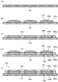
- FIG. 1 is a diagram illustrating one step of a method for manufacturing a solid-state battery.
- FIGS. 1 (A) to 1 (D) schematically show a cross-sectional view of a main part of each step of electrode formation in solid-state battery manufacturing.
- the first electrode layer 10 is formed.
- the first electrode layer 10 is formed, for example, in a cross-sectional view in which the thickness of the inner portion 10b is thicker than the thickness of the end portion 10a.
- the paste prepared for the electrode layer 10 is printed on a predetermined print object (not shown) such as an electrolyte layer by using a screen printing method, and dried. It is formed by that.
- the paste for the first electrode layer 10 includes, for example, an active material, a solid electrolyte, a conductive additive, a binder, a solvent, and the like.
- the first embedded layer 11 is formed at the end portion 10a of the first electrode layer 10 as shown in FIG. 1 (B).
- the first embedded layer 11 is formed so as to embed an end portion 10a thinner than the inner portion 10b of the first electrode layer 10 in a cross-sectional view, for example.
- the embedded layer 11 of the first layer contains a material having an electron conductivity lower than that of the active material contained in the electrode layer 10 of the first layer (and the electrode layer 20 of the second layer described later), for example, an insulating material or a solid electrolyte. Is used. As an example, a material having an electron conductivity of 1 ⁇ 10 -2 S / cm to 1 ⁇ 10-5 S / cm is used for the first electrode layer 10, and the first embedded layer 11 is used as an embedded layer 11. A material having an electron conductivity of 1 ⁇ 10 -9 S / cm to 1 ⁇ 10 -10 S / cm is used.
- the first embedded layer 11 is, for example, a paste prepared for the embedded layer 11 on a region (on the end portion 10a or on the end portion 10a) other than the inner portion 10b of the first layer electrode layer 10 by using a screen printing method. It is formed by printing on the edge 10a and its outer region) and drying.
- the paste for the first embedded layer 11 contains, for example, a solid electrolyte, a binder, a plasticizer, a dispersant, a diluent and the like.
- the second electrode layer 20 is formed as shown in FIG. 1 (C).
- the second electrode layer 20 is formed, for example, in a cross-sectional view in which the thickness of the inner portion 20b is thicker than the thickness of the end portion 20a.
- the paste prepared for the electrode layer 20 is formed on the inner portion 10b of the first electrode layer 10 and at the end portion 10a thereof by using a screen printing method. It is formed by printing on the first embedded layer 11 and drying.
- the paste for the second electrode layer 20 includes, for example, an active material, a solid electrolyte, a conductive additive, a binder, a solvent, and the like.
- the first-layer electrode layer 10 and the second-layer electrode layer 20 are both electrode layers that are part of the positive electrode of the solid-state battery, or both are part of the negative electrode of the solid-state battery. It is an electrode layer. That is, the electrode layer 10 of the first layer and the electrode layer 20 of the second layer both contain a positive electrode active material, or both contain a negative electrode active material.
- the first-layer electrode layer 10 and the second-layer electrode layer 20 are provided so as to be in contact with each other at the inner portion 10b and the inner portion 20b.
- the first embedded layer 11 is provided around the portion 3 where the first electrode layer 10 and the second electrode layer 20 are in contact with each other.
- the second embedded layer 21 is formed at the end portion 20a of the second electrode layer 20 as shown in FIG. 1 (D).
- the second embedded layer 21 is formed so as to embed an end portion 20a thinner than the inner portion 20b of the second electrode layer 20 in a cross-sectional view, for example.
- the second embedded layer 21 contains a material having an electron conductivity lower than that of the active material contained in the second electrode layer 20 (and the third electrode layer described later), for example, an insulating material or a solid electrolyte. Used. As an example, a material having an electron conductivity of 1 ⁇ 10 -2 S / cm to 1 ⁇ 10-5 S / cm is used for the second electrode layer 20, and the second embedded layer 21 is used for the second embedded layer 21. A material having an electron conductivity of 1 ⁇ 10 -9 S / cm to 1 ⁇ 10 -10 S / cm is used.
- the second embedded layer 21 is, for example, a paste prepared for the embedded layer 21 on a region (on the end portion 20a or on the end portion 20a) of the second layer electrode layer 20 excluding the inner portion 20b by using a screen printing method. It is formed by printing on the edge 20a and its outer region) and drying.
- the paste for the second embedded layer 21 includes, for example, a solid electrolyte, a binder, a plasticizer, a dispersant, a diluent and the like.
- Electrodes The number of layers required for the above steps as the positive electrode or the negative electrode of the solid-state battery (hereinafter, one or both of them are simply referred to as “electrodes"), for example, the amount of active material and the film required for the electrode of the solid-state battery to be manufactured. It is repeated for the number of thick layers. For example, when a third electrode layer (not shown) is formed on the second electrode layer 20 so as to be in contact with the inner portion 20b thereof, the second layer is around the portion in contact with them.
- the embedded layer 21 of the above will be provided.
- the electrode 1 of the solid-state battery (in FIG. 1 (D), two electrode layers 10 and 20 are shown as an example) is formed.
- the positive electrode and the negative electrode which are formed by the above steps, are laminated and heat-bonded with an electrolyte layer (for example, a base of the first electrode layer 10) interposed therebetween.
- an electrolyte layer for example, a base of the first electrode layer 10.
- the first embedded layer 11 is provided at the end portion 10a of the first electrode layer 10, and the second electrode layer 20 is provided on the first embedded layer 11.
- the gap between the end 10a of the first electrode layer 10 and the end 20a of the second electrode layer 20 is embedded in the first embedded layer 11 and the second electrode layer is formed.
- the end portion 20a of 20 is supported by the first embedded layer 11.
- the gap between the end portion 20a of the second layer electrode layer 20 and the end portion of the third layer electrode layer is the gap of the second layer electrode layer 20. It is embedded by the second embedded layer 21 provided at the end 20a, and the end of the third electrode layer is supported by the second embedded layer 21.
- the end of the upper electrode layer is supported by the embedded layer embedded in the end of the lower electrode layer, so that the electrode Deformation of the electrode layer group in each electrode during lamination and thermal pressure bonding after formation is suppressed.
- the deformation of each electrode and its electrode layer group at the time of thermal pressure bonding contact between the electrode pairs laminated with the electrolyte layer interposed therebetween, that is, the contact between the positive electrode and the negative electrode is suppressed.
- the occurrence of a short circuit inside the solid-state battery is effectively suppressed.
- the electrode including the laminated body of the electrode layer group as described above has a recess (a portion corresponding to the above gap) between the end portion of the lower layer side electrode layer and the end portion of the upper layer side electrode layer.
- the recess has a structure in which an embedded layer having a lower electron conductivity than the lower layer side and upper layer side electrode layers is provided.
- a solid-state battery having an electrode having such a structure as a positive electrode or a negative electrode it becomes difficult for a current to flow to a side end portion (end portion of each electrode layer of the laminated body) of the electrode where electrical conductivity tends to vary. As a result, the performance variation among the manufactured solid-state battery groups can be suppressed.
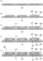
- FIG. 2 is a diagram illustrating an example of electrodes of a solid-state battery.
- 2 (A) and 2 (B) schematically show a cross-sectional view of a main part of an example of an electrode of a solid-state battery.
- the electrodes 1 (each of the positive electrode and the negative electrode) of the solid-state battery formed by using the steps shown in FIGS. 1 (A) to 1 (D) are shown in FIG. 2 (A), for example.
- the first layer LY1 and the second layer LY2 are included.
- the first layer LY1 includes the first electrode layer 10 and the first embedded layer 11 provided at the end portion 10a thereof.
- the second layer LY2 includes a second electrode layer 20 and a second embedded layer 21 provided at the end portion 20a thereof.
- the electrodes 1 (each of the positive electrode and the negative electrode) of the solid-state battery formed by using the steps shown in FIGS. 1 (A) to 1 (D) are, for example, FIG. 2 (B).
- the first region AR1 and the second region AR2 are included.
- the first region AR1 includes an inner portion 10b of the first electrode layer 10 and an inner portion 20b of the second electrode layer 20.
- the portion 3 in which the first electrode layer 10 and the second electrode layer 20 are in contact with each other exists in the first region AR1.
- the second region AR2 is a region around the first region AR1. In the second region AR2, the end portion 10a of the first layer electrode layer 10 and the first embedded layer 11 provided therein, and the end portion 20a of the second layer electrode layer 20 and the end portion 20a provided therein are provided.
- a second embedded layer 21 is included.
- a recess 4 recessed on the first region AR1 side is formed between the end portion 10a of the first layer electrode layer 10 and the end portion 20a of the second layer electrode layer 20 of the second region AR2. It is formed, and the first embedded layer 11 is formed in the recess 4.
- a recess 4 is formed between the end 20a of the second electrode layer 20 and the end of the third electrode layer, and the second layer is embedded in the recess 4.
- Layer 21 is formed.
- the electrode 1 of such a solid-state battery in the second region AR2 including the embedded layer 11 and the embedded layer 21, deformation of the electrode layer 10 and the electrode layer 20 during lamination and heat bonding is suppressed, and the solid caused by the deformation. The occurrence of battery short circuit is suppressed. Further, in the electrode 1, it becomes difficult for a current to flow in the second region AR2 in which the electrical conductivity tends to vary as compared with the first region AR1, and the performance variation among the solid-state battery groups including the electrode 1 can be suppressed.
- FIGS. 2 (A) and 2 (B) illustrate the boundary between the inner portion 10b of the first electrode layer 10 and the inner portion 20b of the second electrode layer 20.
- firing can be performed.
- the inner portion 10b of the first electrode layer 10 and the inner portion 20b of the second electrode layer 20 are sintered and integrated by such firing at the portion 3 in contact with them. May be.
- the first electrode layer 10, the first embedded layer 11, the second electrode layer 20, and the second embedded layer 21 are mentioned.
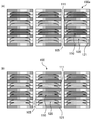
- the electrodes 1 are formed in order, the order of formation is not limited to the above example. This point will be described with reference to FIG. 3 below.
- FIG. 3 is a diagram illustrating another example of electrodes of a solid-state battery. 3 (A) and 3 (B), respectively, schematically show a cross-sectional view of a main part of an example of an electrode.
- the first embedded layer 11 is formed by using, for example, a screen printing method, and then the first electrode layer 10 is formed, for example.
- the first layer LY1 is formed by being formed by using the screen printing method.
- the second embedded layer 21 is formed by using, for example, a screen printing method, and then the second electrode layer 20 is formed by using, for example, a screen printing method, whereby the second layer LY2 is formed. It is formed. It is also possible to form each layer in such an order to obtain the electrode 1a as shown in FIG. 3 (A).
- the first electrode layer 10 is first formed, then the first embedded layer 11 is formed, and the first layer LY1 is formed. NS.
- the second embedded layer 21 is formed, then the second electrode layer 20 is formed, and the second layer LY2 is formed.
- an embedded layer 31 is formed on the outside of the first layer LY1 and the second layer LY2.
- a screen printing method is used to form each layer. It is also possible to form each layer in such an order to obtain the electrode 1b as shown in FIG. 3 (B).
- Example Examples of the solid-state battery and its manufacturing method will be described in detail below. First, an example of forming an electrolyte sheet, a paste for a positive electrode layer, a paste for a negative electrode layer, and a paste for an embedded layer will be described.
- a paste containing a solid electrolyte, a binder, a plasticizer, a dispersant and a diluent is used to form the electrolyte sheet.
- the solid electrolyte of the paste for the electrolyte sheet includes, for example, Li 1.5 Al 0.5 Ge 1.5 (PO 4 ) 3 (hereinafter, one of the NASICON type oxide-based solid electrolytes). "LAGP”) is used. LAGP is also referred to as aluminum-substituted germanium lithium phosphate or the like.
- the paste for an electrolyte sheet contains 29.0 wt% (% by weight) of amorphous LAGP (hereinafter referred to as “LAGPg”) and 3 of crystalline LAGP (hereinafter referred to as “LAGPc”) as solid electrolytes. .2 wt%, PVB 6.5 wt% as binder, 2.2 wt% plasticizer, 0.3 wt% first dispersant, 16.1 wt% second dispersant, 43.4 wt% ethanol as diluent % Is used.
- One kind of material may be used for each of the binder, the plasticizer, the dispersant and the diluent of the paste for the electrolyte sheet, or two or more kinds of materials may be used.
- the component material of the electrolyte sheet paste as described above is mixed and dispersed, for example, mixed and dispersed in a ball mill for 48 hours to form the electrolyte sheet paste.
- the formed electrolyte sheet paste is coated and dried, for example, coated using a sheet molding machine such as a doctor blade, and dried at a temperature of 100 ° C. for 10 minutes to form an electrolyte sheet.
- paste for positive electrode layer As the paste for the positive electrode layer, a paste containing a positive electrode active material, a solid electrolyte, a conductive auxiliary agent, a binder, a plasticizer, a dispersant and a diluent is used.
- lithium cobalt pyrophosphate Li 2 CoP 2 O 7 , hereinafter referred to as “LCPO”
- LCPO lithium cobalt pyrophosphate
- the cathode active material lithium cobalt oxide (LiCoPO 4 ), lithium vanadium phosphate (Li 3 V 2 (PO 4 ) 3 ) (hereinafter referred to as “LVP”) and the like may be used.
- LVP lithium vanadium phosphate
- the positive electrode active material one kind of material may be used, or two or more kinds of materials may be used.
- LAGP is used as the solid electrolyte of the paste for the positive electrode layer.
- the conductive auxiliary agent for the positive electrode layer paste for example, a carbon material such as carbon nanofiber, carbon black, graphite, graphene, or carbon nanotube is used.
- the paste for the positive electrode layer contains 11.8 wt% of LCPO as the positive electrode active material, 17.7 wt% of LAGPg as the solid electrolyte, 2.7 wt% of carbon nanofibers as the conductive auxiliary agent, and 7.V B as the binder.
- Those containing 9 wt%, 0.3 wt% of plasticizer, 0.6 wt% of first dispersant, and 59.1 wt% of tarpineol as a diluent are used.
- One kind of material may be used for each of the binder, the plasticizer, the dispersant and the diluent of the paste for the positive electrode layer, or two or more kinds of materials may be used.
- the component materials of the above-mentioned positive electrode layer paste are mixed and dispersed, for example, for 72 hours in a ball mill and mixed and dispersed in a three-roll mill, and mixed and dispersed using a grain gauge until the aggregate becomes 1 ⁇ m or less. Then, the paste for the positive electrode layer is formed.
- paste for negative electrode layer As the paste for the negative electrode layer, a paste containing a negative electrode active material, a solid electrolyte, a conductive auxiliary agent, a binder, a plasticizer, a dispersant and a diluent is used.
- anatase-type titanium oxide (TiO 2 ) is used as the negative electrode active material of the negative electrode layer paste.
- the negative electrode active material Li 1.3 Al 0.3 Ti 1.7 (PO 4 ) 3 (hereinafter referred to as “LATP”), LVP, etc., which are one of the NASICON type oxide-based solid electrolytes, are used. You may.
- LATP Li 1.3 Al 0.3 Ti 1.7 (PO 4 ) 3
- LVP LVP
- the negative electrode active material one kind of material may be used, or two or more kinds of materials may be used.
- LAGP is used as the solid electrolyte of the paste for the negative electrode layer.
- the conductive auxiliary agent of the paste for the negative electrode layer for example, a carbon material such as carbon nanofiber, carbon black, graphite, graphene, and carbon nanotube is used.
- the paste for the negative electrode layer contains 11.8 wt% of TiO 2 as the negative electrode active material, 17.7 wt% of LAGPg as the solid electrolyte, 2.7 wt% of carbon nanofibers as the conductive auxiliary agent, and 7 PVB as the binder. .9 wt%, 0.3 wt% plasticizer, 0.6 wt% first dispersant, and 59.1 wt% tarpineol as a diluent are used.
- One kind of material may be used for each of the binder, the plasticizer, the dispersant and the diluent of the paste for the negative electrode layer, or two or more kinds of materials may be used.
- the constituent materials of the paste for the negative electrode layer as described above are mixed and dispersed, for example, mixed and dispersed in a ball mill for 72 hours and in a three-roll mill, and mixed and dispersed using a grain gauge until the aggregate becomes 1 ⁇ m or less. Then, the paste for the negative electrode layer is formed.
- paste for embedded layer As the paste for the embedded layer, a paste containing a solid electrolyte, a binder, a plasticizer, a dispersant and a diluent is used.
- LAGP is used as the solid electrolyte of the paste for the embedded layer.
- the paste for the embedded layer contains 25.4 wt% of LAGPg and 2.8 wt% of LAGPc as the solid electrolyte, 8.5 wt% of PVB as the binder, 0.2 wt% of the plasticizer, and the first dispersion.
- An agent containing 1.9 wt% and a diluent containing 61.2 wt% of tarpineol are used.
- One kind of material may be used for each of the binder, the plasticizer, the dispersant, and the diluent of the paste for the embedded layer, or two or more kinds of materials may be used.
- the component materials of the paste for the embedded layer as described above are mixed and dispersed, for example, for 72 hours in a ball mill and mixed and dispersed in a three-roll mill, and mixed and dispersed using a grain gauge until the aggregate becomes 1 ⁇ m or less. Then, the paste for the embedded layer is formed.
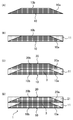
- FIG. 4 is a diagram illustrating an example of a method for forming the positive electrode parts.
- FIG. 4A schematically shows a plan view of a main part of an example of the positive electrode layer forming step.
- FIG. 4B schematically shows a plan view of a main part of an example of the embedded layer forming step.
- the positive electrode layer paste is applied onto the electrolyte sheet 101, and the applied positive electrode layer paste is dried to form the first positive electrode layer 110.
- the coating of the positive electrode layer paste is performed, for example, by using a screen printing method.
- the coated positive electrode layer paste is dried, for example, at a temperature of 90 ° C. for 5 minutes.
- the positive electrode layer 110 (paste for the positive electrode layer) is provided in a plurality of solid-state battery forming regions on one electrolyte sheet 101.
- FIG. 4A shows, as an example, positive electrode layers 110 of two sizes, large and small, in which the small size positive electrode layer 110 is used as the positive electrode layer of one solid-state battery, and the large size positive electrode layer is used. 110 is used as the positive electrode layer of two solid-state batteries.
- each portion (three locations for convenience) used as the positive electrode layer of one solid-state battery is illustrated by a dotted line frame.
- an embedded layer paste is applied around the positive electrode layer 110 on the electrolyte sheet 101, and the applied embedded layer paste is applied. Is dried to form the first embedded layer 111 of the positive electrode part.
- the embedded layer 111 (paste for embedded layer) is formed so as to cover (cover the end) the end of the positive electrode layer 110.
- the coating of the paste for the embedded layer is performed, for example, by using a screen printing method.
- the coated paste for the embedded layer is dried, for example, at a temperature of 90 ° C. for 5 minutes.
- the steps shown in FIGS. 4 (A) and 4 (B) have a predetermined number of layers, for example, the number of layers required to function as a positive electrode of a solid-state battery and the thickness of the active material. This is repeated to form the positive electrode parts.
- FIG. 5 is a diagram illustrating an example of a method for forming the negative electrode parts.
- FIG. 5A schematically shows a plan view of a main part of an example of the negative electrode layer forming step.
- FIG. 5B schematically shows a plan view of a main part of an example of the embedded layer forming step.
- the negative electrode layer paste is applied onto the electrolyte sheet 101, and the applied negative electrode layer paste is dried to form the first negative electrode layer 120.
- the coating of the negative electrode layer paste is performed, for example, by using a screen printing method.
- the coated negative electrode layer paste is dried, for example, at a temperature of 90 ° C. for 5 minutes.
- the negative electrode layer 120 (paste for the negative electrode layer) is provided in a plurality of solid-state battery forming regions on one electrolyte sheet 101.
- FIG. 5A shows a negative electrode layer 120 having one type of size, which is used as a negative electrode layer for two solid-state batteries.
- each portion (three locations for convenience) used as the negative electrode layer of one solid-state battery in the negative electrode layer 120 is shown by a dotted line frame.
- the paste for the embedded layer is coated around the negative electrode layer 120 on the electrolyte sheet 101, and the applied paste for the embedded layer is applied. Is dried to form the first embedded layer 121 of the negative electrode part.
- the embedded layer 121 (paste for embedded layer) is formed so as to cover (cover the end) the end of the negative electrode layer 120.
- the coating of the paste for the embedded layer is performed, for example, by using a screen printing method.
- the coated paste for the embedded layer is dried, for example, at a temperature of 90 ° C. for 5 minutes.
- the steps shown in FIGS. 5 (A) and 5 (B) have a predetermined number of layers, for example, the number of layers required to function as a negative electrode of a solid-state battery and the thickness of the active material. This is repeated to form the negative electrode parts.
- the negative electrode parts, which are formed by repeating the above steps for a predetermined number of layers, are alternately laminated and heat-bonded by a uniaxial press.
- Thermal pressure bonding is performed under the conditions of, for example, a pressure of 20 MPa and a temperature of 45 ° C.
- the formed laminated green is cut at a predetermined position using a cutting machine, and then degreased by heat treatment under the condition of holding at a temperature of 500 ° C. for 10 hours in an oxygen-containing atmosphere, and further contains nitrogen. Sintering is performed by heat treatment under the condition of holding at 600 ° C. for 2 hours in an atmosphere. As a result, a solid-state battery is obtained.
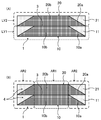
- FIG. 6 and 7 are diagrams for explaining a configuration example of a solid-state battery.
- FIG. 6 (A) schematically shows an external perspective view of the solid-state battery
- FIG. 6 (B) schematically shows an example of a cut surface along the surface P1 as shown in FIG. 6 (A).
- FIG. 6C schematically shows an external perspective view of a solid-state battery provided with an external terminal.
- FIG. 7 (A) schematically shows an external perspective view of the solid-state battery
- FIG. 7 (B) schematically shows an example of a cut surface along the surface P2 as shown in FIG. 7 (A). Shown.
- the solid-state battery 100 shown in FIGS. 6 (A) and 7 (A) is manufactured by cutting the laminated green body using a cutting machine and performing heat treatment.
- the laminated body green has a structure in which positive electrode parts 115 and negative electrode parts 125 are alternately laminated and heat-bonded as shown in FIGS. 6 (B) and 7 (B).
- the positive electrode component 115 includes an electrolyte sheet 101 (electrolyte layer 105) and a plurality of layers (for example, two layers) of positive electrode layers 110 and embedded layers 111 provided on the electrolyte sheet 101.
- the negative electrode component part 125 includes an electrolyte sheet 101 (electrolyte layer 105) and a plurality of layers (for example, two layers) of negative electrode layers 120 and an embedded layer 121 provided on the electrolyte sheet 101.
- Such a laminated green is cut as shown in FIGS. 6 (B) and 7 (B), and at that time, as shown in FIG. 6 (B), the positive electrode layer 110 is exposed on one end surface.
- the solid-state battery 100 is obtained by cutting the other end surface at a position where the negative electrode layer 120 is exposed and further performing heat treatment.
- the positive electrode layers 110 of the plurality of layers (two layers as an example) of each positive electrode part 115 and the negative electrode layers 120 of the multiple layers (two layers as an example) of each negative electrode part 125 are, for example, lined after cutting. It is sintered and integrated by the heat treatment. A part of the embedded layer 111 is interposed between the ends 110a of the positive electrode layers 110 of each positive electrode part 115, and a part of the embedded layer 121 is interposed between the ends 120a of the negative electrode layers 120 of each of the negative electrode parts 125. Will be done.
- the positive electrode terminal surface 130 includes a side end surface of the positive electrode layer 110 of the positive electrode part 115, a side end surface of the electrolyte layer 105 obtained by cutting the electrolyte sheet 101, and a side end surface of the embedded layer 121 of the negative electrode part 125. It is exposed and the negative electrode layer 120 is not exposed.
- the side end surface of the negative electrode layer 120 of the negative electrode part 125, the side end surface of the electrolyte layer 105, and the side end surface of the embedded layer 111 of the positive electrode part 115 are exposed on the negative electrode terminal surface 140, and the positive electrode layer 110 is not exposed.
- the positive electrode layer 110 of the positive electrode component 115 And the negative electrode layer 120 of the negative electrode component 125 are alternately laminated via the electrolyte layer 105.
- Positive electrode terminal 131 and negative electrode terminal 141 are formed as external terminals.
- the positive electrode terminal 131 is formed so as to be connected to the side end surface of the positive electrode layer 110 exposed on the positive electrode terminal surface 130
- the negative electrode terminal 141 is connected to the side end surface of the negative electrode layer 120 exposed to the negative electrode terminal surface 140. Is formed in.
- a chip-type solid-state battery 100 is realized in which a plurality of battery cells including a pair of a positive electrode layer 110 and a negative electrode layer 120 and an electrolyte layer 105 between them are electrically connected in parallel.
- terminal surface vertical direction the cut surface along the surface P1 of FIG. 6A, that is, the direction perpendicular to the positive electrode terminal surface 130 and the negative electrode terminal surface 140
- terminal surface parallel direction the cut surface along the surface P2 of FIG. 7 (A), that is, the direction parallel to the positive electrode terminal surface 130 and the negative electrode terminal surface 140
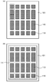
- FIG. 8 is a diagram showing an example of a process of forming a positive electrode part in a cross section in the vertical direction of the terminal surface
- FIG. 9 is a diagram showing an example of a process of forming a negative electrode component in a cross section in the vertical direction of the terminal surface
- FIG. FIG. 11 is a diagram showing an example of a layered green forming step in a cross section in the direction
- FIG. 11 is a diagram showing an example of a cutting step and a heat treatment step in the cross section in the direction perpendicular to the terminal surface.
- FIG. 12 is a diagram showing an example of a process of forming a positive electrode part in a cross section parallel to the terminal surface
- FIG. 13 is a diagram showing an example of a process of forming a negative electrode part in a cross section parallel to the terminal surface
- FIG. 14 is a diagram showing an example of a process of forming a negative electrode part in a cross section parallel to the terminal surface
- FIG. 15 is a diagram showing an example of a layered green forming step in a cross section in the direction
- FIG. 15 is a diagram showing an example of a cutting step and a heat treatment step in the cross section in the direction parallel to the terminal surface. 12 (A) to 12 (E), 13 (A) to 13 (E), 14 (A) to 14 (C), and 15 (A) and 15 (B).
- the cross-sectional view of the main part of each process is schematically shown.
- a paste for the positive electrode layer was applied to a predetermined region (region for forming a plurality of solid-state batteries) on the electrolyte sheet 101 by using a screen printing method.
- the first positive electrode layer 110 is formed.
- the first positive electrode layer 110 formed in each region by the screen printing method has a shape such that the thickness of the inner portion 110b is thicker than the thickness of the end portion 110a on the entire circumference thereof, and is an electrolyte sheet. Formed on 101.
- an embedding layer paste is applied around the positive electrode layer 110 of the first layer on the electrolyte sheet 101 by a screen printing method. Is dried to form the first embedded layer 111.
- the first embedded layer 111 is formed so as to cover the end 110a of the first positive electrode layer 110 and expose the inner portion 110b thereof.
- a positive electrode layer paste is applied onto the positive electrode layer 110 of the first layer by a screen printing method, and the paste is dried.
- the second positive electrode layer 110 is formed so as to be laminated on the first positive electrode layer 110.
- the second positive electrode layer 110 is also formed in such a shape that the thickness of the inner portion 110b is thicker than the thickness of the end portion 110a on the entire circumference thereof. ..
- a part of the first embedded layer 111 formed so as to cover the end 110a of the first positive electrode layer 110 between the end 110a of the first layer and the second positive electrode layer 110. Intervenes.
- an embedding layer paste is applied around the positive electrode layer 110 of the second layer by a screen printing method, and the paste is dried. Then, the second embedded layer 111 is formed. The second embedded layer 111 is formed so as to cover the end 110a of the second positive electrode layer 110 and expose the inner portion 110b thereof.
- a plurality of layers (two layers in this example) of the positive electrode layers 110 are laminated by the steps shown in FIGS. 8 (A) to 8 (E) and FIGS. 12 (A) to 12 (E).
- a positive electrode part 115 having a structure in which the end portions 110a of the above are each covered with an embedded layer 111 is formed.
- a paste for the negative electrode layer is applied to a predetermined region (region for forming a plurality of solid-state batteries) on the electrolyte sheet 101 by using a screen printing method.
- the first negative electrode layer 120 is formed.
- the first negative electrode layer 120 formed in each region by the screen printing method has a shape such that the thickness of the inner portion 120b is thicker than the thickness of the end portion 120a on the entire circumference thereof, and is an electrolyte sheet. Formed on 101.
- an embedding layer paste is applied around the negative electrode layer 120 of the first layer on the electrolyte sheet 101 by a screen printing method. Is dried to form the first embedded layer 121.
- the first embedded layer 121 is formed so as to cover the end portion 120a of the first negative electrode layer 120 and expose the inner portion 120b thereof.
- a paste for the negative electrode layer is applied onto the negative electrode layer 120 of the first layer by a screen printing method, and the paste is dried.
- the second negative electrode layer 120 is formed so as to be laminated on the first negative electrode layer 120.
- the second negative electrode layer 120 is also formed in such a shape that the thickness of the inner portion 120b is thicker than the thickness of the end portion 120a on the entire circumference thereof. ..
- a part of the first embedded layer 121 formed so as to cover the end 120a of the first negative electrode layer 120 between the ends 120a of the first and second negative electrode layers 120. Intervenes.
- the paste for the embedded layer is applied around the negative electrode layer 120 of the second layer by a screen printing method, and the paste for the embedded layer is dried. Then, the second embedded layer 121 is formed. The second embedded layer 121 is formed so as to cover the end portion 120a of the second negative electrode layer 120 and expose the inner portion 120b thereof.
- a plurality of layers (two layers in this example) of the negative electrode layers 120 are laminated by the steps shown in FIGS. 9 (A) to 9 (E) and 13 (A) to 13 (E).
- a negative electrode part 125 having a structure in which each end portion 120a of the above is covered with an embedded layer 121 is formed.
- the positive electrode parts 115 and the negative electrode parts 125 obtained as described above are alternately laminated and heat-bonded to form a laminated green.
- the positive electrode part 115 of the first layer is laminated on the negative electrode part 125 of the first layer, and further, the positive electrode part 115 of FIG. 10B and FIG. 14
- the second layer negative electrode part 125 is laminated on the first layer positive electrode part 115.
- the second-layer positive electrode part 115 is laminated on the second-layer negative electrode part 125, and the electrolyte sheet 101 is further formed on the uppermost layer. Stacked. By heat-bonding these, the laminated body green 150 is formed.
- FIGS. 10 (A) to 10 (C) the cross section in the direction perpendicular to the terminal surface (cross section along the plane P1 of FIG. 6 (A)) is shown in FIGS. 10 (A) to 10 (C).
- the negative electrode part 125 and the positive electrode part 115 are laminated so that the opposing negative electrode layers 120 and the positive electrode layers 110 partially overlap each other. That is, in a cross-sectional view in the direction perpendicular to the terminal surface, the upper positive electrode layer 110 is located so as to straddle the adjacent negative electrode layers 120 of the lower layer, and the upper negative electrode layer 120 straddles the adjacent positive electrode layers 110 of the lower layer.
- the negative electrode part 125 and the positive electrode part 115 are laminated so as to be located.
- the negative electrode layer 120 and the positive electrode layer 110 have a positional relationship that partially overlaps in the cross section in the direction perpendicular to the terminal surface. As described above, screen printing is performed.
- each negative electrode layer 120 and each positive electrode layer 110 are laminated so as to overlap with each other as a whole.
- the negative electrode layer 120 and the positive electrode layer 110 have a positional relationship that overlaps as a whole in the cross section in the direction parallel to the terminal plane. As described above, screen printing is performed.
- the laminate green 150 obtained as described above is cut at the position DL1 as shown by the chain line in FIGS. 10 (C) and 14 (C) above using a cutting machine. As a result, a plurality of individual pieces 150a of the laminated green 150 as shown in FIGS. 11 (A) and 15 (A) are formed. Further, by performing heat treatment for degreasing and firing, the individual solid-state batteries 100 as shown in FIGS. 11 (B) and 15 (B) (and FIGS. 6 (B) and 7 (B)). Is formed.
- Each solid-state battery 100 includes a plurality of battery cells in which a cut electrolyte sheet 101 is provided as an electrolyte layer 105, and a positive electrode layer 110 and a negative electrode layer 120 are provided via the electrolyte layer 105.
- the negative electrode layers 120 laminated in each negative electrode part 125 are integrated by sintering, and the positive electrode layers 110 laminated in each positive electrode part 115 are burnt.
- the structure is integrated by the connection.
- the side end surface of the positive electrode layer 110 is exposed on one end surface of each solid-state battery 100 in the vertical direction of the terminal surface, and the other end surface of each solid-state battery 100 in the vertical direction of the terminal surface is exposed.
- the side end face of the negative electrode layer 120 is exposed. That is, in the direction perpendicular to the terminal surface, the side where the side end surface of the positive electrode layer 110 is exposed is the positive electrode terminal surface 130, and the side where the side end surface of the negative electrode layer 120 is exposed is the negative electrode terminal surface 140.
- the chip-shaped solid-state battery 100 is realized by forming the positive electrode terminal 131 and the negative electrode terminal 141 as shown in FIG. 6C above on the positive electrode terminal surface 130 and the negative electrode terminal surface 140, respectively.
- the positive electrode layer 110 when a plurality of positive electrode layers 110 are laminated to obtain a positive electrode component part 115, the positive electrode layer 110 is embedded in an end portion 110a thinner than the inner portion 110b thereof. After covering with, stack. Similarly, when a plurality of negative electrode layers 120 are laminated to obtain a negative electrode component part 125, the negative electrode layer 120 is laminated after covering the end portion 120a thinner than the inner portion 120b with the embedded layer 121.
- the positive electrode layer 110 is heat-bonded as compared with the case where the embedded layer 111 is not provided at the end 110a. Deformation of time is suppressed.
- the negative electrode layer 120 is suppressed from being deformed during thermal pressure bonding as compared with the case where the embedded layer 121 is not provided at the end portion 120a thereof. Further, the deformation of the positive electrode layer 110 and the negative electrode layer 120 during the subsequent heat treatment can be suppressed, and further, the deformation of the electrolyte layer 105 located between them can be suppressed. By suppressing the deformation of the positive electrode layer 110, the negative electrode layer 120, and the like, the occurrence of a short circuit in the solid-state battery 100 due to the deformation is effectively suppressed.
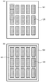
- FIG. 16 is a diagram illustrating an electrode configuration of a solid-state battery.
- FIG. 16A schematically shows a cross-sectional view of a main part of the solid-state battery
- FIG. 16B schematically shows a partially enlarged view of the Q part (one electrode layer) of FIG. 16A.
- 16 (C) schematically shows a perspective view of the Q portion of FIG. 16 (A).
- a solid-state battery 160 having a structure as shown in FIG. 16 (A) is used for the investigation.
- 10 electrode layers 170 corresponding to the positive electrode layer 110 or the negative electrode layer 120
- an embedded layer 180 embedded layer 111 or the embedded layer 121 described above
- FIG. 16A shows only one layer of the electrolyte layer 105 and 10 layers of the electrode layer 170 and the embedded layer 180 provided on one surface side thereof.
- 16 (B) and 16 (C) show the region (Q part) including the electrode layer 170 for one layer in such a solid-state battery 160.
- the distance from the side end of the electrode layer 170 of the embedded layer 180 overlaid on the end 170a of the electrode layer 170 as shown in FIG. 16B is defined as the “covering distance d”.
- the thickness of the inner portion 170b of the electrode layer 170 is defined as “electrode thickness t1”, and the thickness of the side edge of the electrode layer 170 is defined as “end thickness t2”. ..
- the five types of solid-state batteries 160 having structures A to E with different covering distances d were formed, and investigations were conducted on them.
- the five types of solid-state batteries 160 have a larger covering distance d in the order of structures A, B, C, D, and E.
- the covering distance d was 15.6 ⁇ m on average, and the covering ratio y was 1.4% on average (Table 1).
- the covering distance d was 24.1 ⁇ m on average, and the covering ratio y was 2.2% on average (Table 1).
- the covering distance d was 34.2 ⁇ m on average, and the covering ratio y was 3.2% on average (Table 1).
- the covering distance d was 61.9 ⁇ m on average, and the covering ratio y was 5.7% on average (Table 2).
- the covering distance d was 77.4 ⁇ m on average, and the covering ratio y was 7.1% on average (Table 2).
- FIG. 17 (A) to 17 (E) are simulated cross-sectional photographs obtained for each of the solid-state batteries 160 of the structures A to E.
- FIGS. 17A to 17C in the structures A, B, and C in which the covering ratio y (average) of the embedded layer 180 covering the end 170a of the electrode layer 170 is relatively small, the electrode layer is used. A large electrode deformation was observed at the end 170a of 170.
- FIGS. 17D and 17E in the structures D and E in which the covering ratio y (average) of the embedded layer 180 covering the end 170a of the electrode layer 170 is relatively large, No large electrode deformation was observed at the end 170a of the electrode layer 170.
- the minimum covering ratio y in the structure D and the structure E in which no large electrode deformation is observed is 4.9% (measurement No. 6 in the structure D), and the maximum covering ratio y is 7.8% (measurement No. 6 in the structure E). Met.
- the covering ratio y is set to be in the range of 4.9% ⁇ y ⁇ 7.8%, which is the minimum and maximum range of the structure D.
- the covering distance d can be specified.
- Solid-state battery defect rate For each solid-state battery 160 of structures A to E, the defect rate [%] due to an internal short circuit was investigated from the initial battery voltage.
- the initial potential is about minus several mV to minus 100 mV, but here, the initial potential is measured and the value is 0 V to ⁇ .
- the solid-state battery 160 having a potential of 0.1 mV was regarded as defective due to an internal short circuit.
- Arbitrarily 30 solid-state batteries 160 formed in each of the structures A to E were extracted and the voltage was measured with a tester. Calculated as. The results are shown in Tables 3 and 4.
- the defect rate of structure A was 93.3%
- the defect rate of structure B was 83.3%
- the defect rate of structure C was 70.0%.
- the defective rate was 6.7% (Table 4). It can be said that by adopting the covering distance d and the covering ratio y such as the structures D and E for the solid-state battery 160, it is possible to realize the solid-state battery 160 in which the electrode deformation and the defect rate are suppressed.
- the thickness difference ratio x [%] was investigated.
- the electrode thickness t1 is the thickness of the inner portion 170b of the electrode layer 170
- the end thickness t2 is the thickness of the side edge of the electrode layer 170 (FIG. 16B).
- the minimum thickness difference ratio x is 7.5% and the maximum thickness difference ratio x is 79.9% in the structure A, and the minimum thickness difference ratio x is in the structure B.
- the maximum thickness difference ratio x was 66.1%
- the minimum thickness difference ratio x was 1.0%
- the maximum thickness difference ratio x was 80.9% (Table 5).
- the minimum thickness difference ratio x was 0.0%
- the maximum thickness difference ratio x was 9.4% in the structure D
- the minimum in the structure E was 1.0% and the maximum thickness difference ratio x was 6.2% (Table 6).
- the electrode layer 170 is adopted so that the thickness difference ratio x between the electrode thickness t1 and the end thickness t2 is in the range of 0% ⁇ x ⁇ 9.4%. It can be said that it is possible to realize the solid-state battery 160 in which the electrode deformation and the defect rate are suppressed by adopting the covering distance d and the covering ratio y such as the structures D and E.
- Electrodes 3 Contact parts 4 Recesses 10, 20, 170 Electrode layers 10a, 20a, 110a, 120a, 170a Ends 10b, 20b, 110b, 120b, 170b Inner parts 11,21,31,111,121, 180 Embedded layer 100, 160 Solid cell 101 Electrode sheet 105 Electrode layer 110 Positive electrode layer 115 Positive electrode parts 120 Negative electrode layer 125 Negative electrode parts 130 Positive electrode terminal surface 131 Positive electrode terminal 140 Negative electrode terminal surface 141 Negative electrode terminal 150 Laminated green 150a Piece AR1 1st region AR2 2nd region LY1 1st layer LY2 2nd layer P1, P2 Surface DL1 Position S0, S1 Area t1 Electrode thickness t2 Edge thickness x Thickness difference ratio d Covering distance y Covering ratio
Landscapes
- Chemical & Material Sciences (AREA)
- Engineering & Computer Science (AREA)
- General Chemical & Material Sciences (AREA)
- Chemical Kinetics & Catalysis (AREA)
- Electrochemistry (AREA)
- Manufacturing & Machinery (AREA)
- Materials Engineering (AREA)
- General Physics & Mathematics (AREA)
- Inorganic Chemistry (AREA)
- Condensed Matter Physics & Semiconductors (AREA)
- Physics & Mathematics (AREA)
- Secondary Cells (AREA)
- Battery Electrode And Active Subsutance (AREA)
Priority Applications (4)
| Application Number | Priority Date | Filing Date | Title |
|---|---|---|---|
| KR1020227025927A KR20220147580A (ko) | 2020-02-26 | 2020-12-10 | 고체 전지의 제조 방법 및 고체 전지 |
| EP20922385.8A EP4113649A1 (en) | 2020-02-26 | 2020-12-10 | Solid-state battery manufacturing method and solid-state battery |
| CN202080093208.6A CN115039251B (zh) | 2020-02-26 | 2020-12-10 | 固态电池的制造方法和固态电池 |
| US17/854,106 US20220344633A1 (en) | 2020-02-26 | 2022-06-30 | Method of manufacturing solid-state battery and solid-state battery |
Applications Claiming Priority (2)
| Application Number | Priority Date | Filing Date | Title |
|---|---|---|---|
| JP2020030269A JP2021136112A (ja) | 2020-02-26 | 2020-02-26 | 固体電池の製造方法及び固体電池 |
| JP2020-030269 | 2020-02-26 |
Related Child Applications (1)
| Application Number | Title | Priority Date | Filing Date |
|---|---|---|---|
| US17/854,106 Continuation US20220344633A1 (en) | 2020-02-26 | 2022-06-30 | Method of manufacturing solid-state battery and solid-state battery |
Publications (1)
| Publication Number | Publication Date |
|---|---|
| WO2021171736A1 true WO2021171736A1 (ja) | 2021-09-02 |
Family
ID=77490893
Family Applications (1)
| Application Number | Title | Priority Date | Filing Date |
|---|---|---|---|
| PCT/JP2020/046115 WO2021171736A1 (ja) | 2020-02-26 | 2020-12-10 | 固体電池の製造方法及び固体電池 |
Country Status (7)
| Country | Link |
|---|---|
| US (1) | US20220344633A1 (zh) |
| EP (1) | EP4113649A1 (zh) |
| JP (1) | JP2021136112A (zh) |
| KR (1) | KR20220147580A (zh) |
| CN (1) | CN115039251B (zh) |
| TW (1) | TWI741923B (zh) |
| WO (1) | WO2021171736A1 (zh) |
Cited By (1)
| Publication number | Priority date | Publication date | Assignee | Title |
|---|---|---|---|---|
| WO2023047845A1 (ja) * | 2021-09-27 | 2023-03-30 | 太陽誘電株式会社 | 全固体電池 |
Citations (7)
| Publication number | Priority date | Publication date | Assignee | Title |
|---|---|---|---|---|
| JPS6313264A (ja) * | 1986-07-02 | 1988-01-20 | Hitachi Maxell Ltd | 非水電解質二次電池 |
| WO1998038688A1 (en) * | 1997-02-28 | 1998-09-03 | Asahi Kasei Kogyo Kabushiki Kaisha | Nonaqueous secondary battery and method for manufacturing the same |
| JP2009038016A (ja) * | 2007-07-09 | 2009-02-19 | Panasonic Corp | 非水電解質二次電池用電極板およびそれを用いた非水電解質二次電池 |
| JP2012023044A (ja) * | 2011-08-26 | 2012-02-02 | Dainippon Printing Co Ltd | 触媒層−電解質膜積層体の製造方法 |
| JP2012038425A (ja) | 2010-08-03 | 2012-02-23 | Toyota Motor Corp | 電極体の製造方法及び電極体 |
| JP2014116136A (ja) | 2012-12-07 | 2014-06-26 | Samsung R&D Institute Japan Co Ltd | 全固体二次電池 |
| WO2019167559A1 (ja) * | 2018-02-28 | 2019-09-06 | パナソニック株式会社 | 二次電池用の電極、及び、これを用いた二次電池 |
Family Cites Families (14)
| Publication number | Priority date | Publication date | Assignee | Title |
|---|---|---|---|---|
| JP2004241690A (ja) * | 2003-02-07 | 2004-08-26 | Oki Electric Ind Co Ltd | スタック型セル及びその製造方法 |
| JP4352016B2 (ja) * | 2005-03-18 | 2009-10-28 | 株式会社東芝 | 無機固体電解質電池及び無機固体電解質電池の製造方法 |
| JP5492686B2 (ja) * | 2010-07-07 | 2014-05-14 | 大日本スクリーン製造株式会社 | 電池用電極の製造方法、電池の製造方法、電池、車両および電子機器 |
| KR101577881B1 (ko) * | 2011-05-27 | 2015-12-15 | 도요타 지도샤(주) | 바이폴라 전고체 전지 |
| JP5918019B2 (ja) * | 2012-05-18 | 2016-05-18 | 株式会社オハラ | 全固体二次電池 |
| US20150325834A1 (en) * | 2012-07-11 | 2015-11-12 | Toyota Jidosha Kabushiki Kaisha | Method for manufacturing all-solid-state battery |
| JP2014116156A (ja) * | 2012-12-07 | 2014-06-26 | Mitsubishi Electric Corp | 全固体電池及びその製造方法並びにこれを用いた回路基板 |
| JP5929748B2 (ja) * | 2012-12-27 | 2016-06-08 | トヨタ自動車株式会社 | 全固体電池の製造方法 |
| JP2015095350A (ja) * | 2013-11-12 | 2015-05-18 | 三菱電機株式会社 | 積層形全固体電池及びその製造方法 |
| JP6522494B2 (ja) * | 2015-12-24 | 2019-05-29 | アルプスアルパイン株式会社 | 全固体蓄電デバイスおよびその製造方法 |
| JP2017168429A (ja) * | 2016-03-11 | 2017-09-21 | 日立金属株式会社 | バイポーラ積層型全固体リチウム二次電池およびその製造方法 |
| JP2018195523A (ja) * | 2017-05-22 | 2018-12-06 | アルプス電気株式会社 | 全固体型二次電池及び全固体型二次電池の製造方法 |
| KR102440680B1 (ko) * | 2017-05-24 | 2022-09-05 | 현대자동차주식회사 | 쇼트 방지형 전고체 전지의 제조 방법 |
| JP7154847B2 (ja) * | 2018-07-06 | 2022-10-18 | Fdk株式会社 | 全固体電池の製造方法 |
-
2020
- 2020-02-26 JP JP2020030269A patent/JP2021136112A/ja active Pending
- 2020-12-10 KR KR1020227025927A patent/KR20220147580A/ko unknown
- 2020-12-10 EP EP20922385.8A patent/EP4113649A1/en active Pending
- 2020-12-10 CN CN202080093208.6A patent/CN115039251B/zh active Active
- 2020-12-10 WO PCT/JP2020/046115 patent/WO2021171736A1/ja unknown
- 2020-12-28 TW TW109146392A patent/TWI741923B/zh active
-
2022
- 2022-06-30 US US17/854,106 patent/US20220344633A1/en active Pending
Patent Citations (7)
| Publication number | Priority date | Publication date | Assignee | Title |
|---|---|---|---|---|
| JPS6313264A (ja) * | 1986-07-02 | 1988-01-20 | Hitachi Maxell Ltd | 非水電解質二次電池 |
| WO1998038688A1 (en) * | 1997-02-28 | 1998-09-03 | Asahi Kasei Kogyo Kabushiki Kaisha | Nonaqueous secondary battery and method for manufacturing the same |
| JP2009038016A (ja) * | 2007-07-09 | 2009-02-19 | Panasonic Corp | 非水電解質二次電池用電極板およびそれを用いた非水電解質二次電池 |
| JP2012038425A (ja) | 2010-08-03 | 2012-02-23 | Toyota Motor Corp | 電極体の製造方法及び電極体 |
| JP2012023044A (ja) * | 2011-08-26 | 2012-02-02 | Dainippon Printing Co Ltd | 触媒層−電解質膜積層体の製造方法 |
| JP2014116136A (ja) | 2012-12-07 | 2014-06-26 | Samsung R&D Institute Japan Co Ltd | 全固体二次電池 |
| WO2019167559A1 (ja) * | 2018-02-28 | 2019-09-06 | パナソニック株式会社 | 二次電池用の電極、及び、これを用いた二次電池 |
Cited By (1)
| Publication number | Priority date | Publication date | Assignee | Title |
|---|---|---|---|---|
| WO2023047845A1 (ja) * | 2021-09-27 | 2023-03-30 | 太陽誘電株式会社 | 全固体電池 |
Also Published As
| Publication number | Publication date |
|---|---|
| EP4113649A1 (en) | 2023-01-04 |
| TWI741923B (zh) | 2021-10-01 |
| TW202133482A (zh) | 2021-09-01 |
| KR20220147580A (ko) | 2022-11-03 |
| CN115039251A (zh) | 2022-09-09 |
| US20220344633A1 (en) | 2022-10-27 |
| CN115039251B (zh) | 2024-02-06 |
| JP2021136112A (ja) | 2021-09-13 |
Similar Documents
| Publication | Publication Date | Title |
|---|---|---|
| CN112005420B (zh) | 固体电池 | |
| US11349146B2 (en) | All-solid lithium ion secondary battery | |
| JPWO2018181667A1 (ja) | 全固体リチウムイオン二次電池 | |
| US20220006068A1 (en) | Solid-state battery | |
| CN114616697B (zh) | 全固体电池 | |
| JPWO2018062079A1 (ja) | 活物質及び全固体リチウムイオン二次電池 | |
| WO2014042083A1 (ja) | 全固体電池、全固体電池用未焼成積層体、および全固体電池の製造方法 | |
| CN111313079B (zh) | 全固体电池 | |
| CN113508487A (zh) | 全固体电池 | |
| CN113544891A (zh) | 全固体二次电池 | |
| JP6992802B2 (ja) | 全固体リチウムイオン二次電池 | |
| WO2021171736A1 (ja) | 固体電池の製造方法及び固体電池 | |
| US12080847B2 (en) | All-solid-state battery | |
| CN112805863B (zh) | 固体电池 | |
| CN113273015B (zh) | 全固体电池 | |
| US12074277B2 (en) | All-solid-state battery | |
| CN113169375B (zh) | 全固体电池 | |
| WO2013035526A1 (ja) | 全固体電池用積層成形体、全固体電池およびその製造方法 | |
| CN113937349B (zh) | 全固体电池 | |
| CN218918943U (zh) | 电极片、电芯及电池 | |
| WO2024070051A1 (ja) | 固体電池およびその製造方法 | |
| WO2024005181A1 (ja) | 全固体二次電池 | |
| WO2022270042A1 (ja) | 電池の製造方法 | |
| JP2020155288A (ja) | 直列型全固体組電池の製造方法 |
Legal Events
| Date | Code | Title | Description |
|---|---|---|---|
| 121 | Ep: the epo has been informed by wipo that ep was designated in this application |
Ref document number: 20922385 Country of ref document: EP Kind code of ref document: A1 |
|
| NENP | Non-entry into the national phase |
Ref country code: DE |
|
| ENP | Entry into the national phase |
Ref document number: 2020922385 Country of ref document: EP Effective date: 20220926 |