WO2021161526A1 - 半導体装置 - Google Patents
半導体装置 Download PDFInfo
- Publication number
- WO2021161526A1 WO2021161526A1 PCT/JP2020/005878 JP2020005878W WO2021161526A1 WO 2021161526 A1 WO2021161526 A1 WO 2021161526A1 JP 2020005878 W JP2020005878 W JP 2020005878W WO 2021161526 A1 WO2021161526 A1 WO 2021161526A1
- Authority
- WO
- WIPO (PCT)
- Prior art keywords
- conductor
- semiconductor element
- semiconductor device
- electrode
- conductor plate
- Prior art date
- Legal status (The legal status is an assumption and is not a legal conclusion. Google has not performed a legal analysis and makes no representation as to the accuracy of the status listed.)
- Ceased
Links
Images








Classifications
-
- H—ELECTRICITY
- H10—SEMICONDUCTOR DEVICES; ELECTRIC SOLID-STATE DEVICES NOT OTHERWISE PROVIDED FOR
- H10W—GENERIC PACKAGES, INTERCONNECTIONS, CONNECTORS OR OTHER CONSTRUCTIONAL DETAILS OF DEVICES COVERED BY CLASS H10
- H10W40/00—Arrangements for thermal protection or thermal control
- H10W40/20—Arrangements for cooling
- H10W40/25—Arrangements for cooling characterised by their materials
- H10W40/255—Arrangements for cooling characterised by their materials having a laminate or multilayered structure, e.g. direct bond copper [DBC] ceramic substrates
-
- H—ELECTRICITY
- H10—SEMICONDUCTOR DEVICES; ELECTRIC SOLID-STATE DEVICES NOT OTHERWISE PROVIDED FOR
- H10D—INORGANIC ELECTRIC SEMICONDUCTOR DEVICES
- H10D80/00—Assemblies of multiple devices comprising at least one device covered by this subclass
- H10D80/20—Assemblies of multiple devices comprising at least one device covered by this subclass the at least one device being covered by groups H10D1/00 - H10D48/00, e.g. assemblies comprising capacitors, power FETs or Schottky diodes
-
- H—ELECTRICITY
- H10—SEMICONDUCTOR DEVICES; ELECTRIC SOLID-STATE DEVICES NOT OTHERWISE PROVIDED FOR
- H10W—GENERIC PACKAGES, INTERCONNECTIONS, CONNECTORS OR OTHER CONSTRUCTIONAL DETAILS OF DEVICES COVERED BY CLASS H10
- H10W70/00—Package substrates; Interposers; Redistribution layers [RDL]
- H10W70/60—Insulating or insulated package substrates; Interposers; Redistribution layers
- H10W70/62—Insulating or insulated package substrates; Interposers; Redistribution layers characterised by their interconnections
- H10W70/65—Shapes or dispositions of interconnections
-
- H—ELECTRICITY
- H10—SEMICONDUCTOR DEVICES; ELECTRIC SOLID-STATE DEVICES NOT OTHERWISE PROVIDED FOR
- H10W—GENERIC PACKAGES, INTERCONNECTIONS, CONNECTORS OR OTHER CONSTRUCTIONAL DETAILS OF DEVICES COVERED BY CLASS H10
- H10W40/00—Arrangements for thermal protection or thermal control
-
- H—ELECTRICITY
- H10—SEMICONDUCTOR DEVICES; ELECTRIC SOLID-STATE DEVICES NOT OTHERWISE PROVIDED FOR
- H10W—GENERIC PACKAGES, INTERCONNECTIONS, CONNECTORS OR OTHER CONSTRUCTIONAL DETAILS OF DEVICES COVERED BY CLASS H10
- H10W70/00—Package substrates; Interposers; Redistribution layers [RDL]
- H10W70/01—Manufacture or treatment
- H10W70/05—Manufacture or treatment of insulating or insulated package substrates, or of interposers, or of redistribution layers
-
- H—ELECTRICITY
- H10—SEMICONDUCTOR DEVICES; ELECTRIC SOLID-STATE DEVICES NOT OTHERWISE PROVIDED FOR
- H10W—GENERIC PACKAGES, INTERCONNECTIONS, CONNECTORS OR OTHER CONSTRUCTIONAL DETAILS OF DEVICES COVERED BY CLASS H10
- H10W70/00—Package substrates; Interposers; Redistribution layers [RDL]
- H10W70/01—Manufacture or treatment
- H10W70/05—Manufacture or treatment of insulating or insulated package substrates, or of interposers, or of redistribution layers
- H10W70/093—Connecting or disconnecting other interconnections thereto or therefrom, e.g. connecting bond wires or bumps
-
- H—ELECTRICITY
- H10—SEMICONDUCTOR DEVICES; ELECTRIC SOLID-STATE DEVICES NOT OTHERWISE PROVIDED FOR
- H10W—GENERIC PACKAGES, INTERCONNECTIONS, CONNECTORS OR OTHER CONSTRUCTIONAL DETAILS OF DEVICES COVERED BY CLASS H10
- H10W70/00—Package substrates; Interposers; Redistribution layers [RDL]
- H10W70/60—Insulating or insulated package substrates; Interposers; Redistribution layers
- H10W70/611—Insulating or insulated package substrates; Interposers; Redistribution layers for connecting multiple chips together
-
- H—ELECTRICITY
- H10—SEMICONDUCTOR DEVICES; ELECTRIC SOLID-STATE DEVICES NOT OTHERWISE PROVIDED FOR
- H10W—GENERIC PACKAGES, INTERCONNECTIONS, CONNECTORS OR OTHER CONSTRUCTIONAL DETAILS OF DEVICES COVERED BY CLASS H10
- H10W70/00—Package substrates; Interposers; Redistribution layers [RDL]
- H10W70/60—Insulating or insulated package substrates; Interposers; Redistribution layers
- H10W70/611—Insulating or insulated package substrates; Interposers; Redistribution layers for connecting multiple chips together
- H10W70/614—Insulating or insulated package substrates; Interposers; Redistribution layers for connecting multiple chips together the multiple chips being integrally enclosed
-
- H—ELECTRICITY
- H10—SEMICONDUCTOR DEVICES; ELECTRIC SOLID-STATE DEVICES NOT OTHERWISE PROVIDED FOR
- H10W—GENERIC PACKAGES, INTERCONNECTIONS, CONNECTORS OR OTHER CONSTRUCTIONAL DETAILS OF DEVICES COVERED BY CLASS H10
- H10W72/00—Interconnections or connectors in packages
- H10W72/30—Die-attach connectors
-
- H—ELECTRICITY
- H10—SEMICONDUCTOR DEVICES; ELECTRIC SOLID-STATE DEVICES NOT OTHERWISE PROVIDED FOR
- H10W—GENERIC PACKAGES, INTERCONNECTIONS, CONNECTORS OR OTHER CONSTRUCTIONAL DETAILS OF DEVICES COVERED BY CLASS H10
- H10W72/00—Interconnections or connectors in packages
- H10W72/90—Bond pads, in general
-
- H—ELECTRICITY
- H10—SEMICONDUCTOR DEVICES; ELECTRIC SOLID-STATE DEVICES NOT OTHERWISE PROVIDED FOR
- H10W—GENERIC PACKAGES, INTERCONNECTIONS, CONNECTORS OR OTHER CONSTRUCTIONAL DETAILS OF DEVICES COVERED BY CLASS H10
- H10W90/00—Package configurations
-
- H—ELECTRICITY
- H10—SEMICONDUCTOR DEVICES; ELECTRIC SOLID-STATE DEVICES NOT OTHERWISE PROVIDED FOR
- H10W—GENERIC PACKAGES, INTERCONNECTIONS, CONNECTORS OR OTHER CONSTRUCTIONAL DETAILS OF DEVICES COVERED BY CLASS H10
- H10W90/00—Package configurations
- H10W90/701—Package configurations characterised by the relative positions of pads or connectors relative to package parts
-
- H—ELECTRICITY
- H10—SEMICONDUCTOR DEVICES; ELECTRIC SOLID-STATE DEVICES NOT OTHERWISE PROVIDED FOR
- H10W—GENERIC PACKAGES, INTERCONNECTIONS, CONNECTORS OR OTHER CONSTRUCTIONAL DETAILS OF DEVICES COVERED BY CLASS H10
- H10W40/00—Arrangements for thermal protection or thermal control
- H10W40/70—Fillings or auxiliary members in containers or in encapsulations for thermal protection or control
- H10W40/77—Auxiliary members characterised by their shape
- H10W40/778—Auxiliary members characterised by their shape in encapsulations
-
- H—ELECTRICITY
- H10—SEMICONDUCTOR DEVICES; ELECTRIC SOLID-STATE DEVICES NOT OTHERWISE PROVIDED FOR
- H10W—GENERIC PACKAGES, INTERCONNECTIONS, CONNECTORS OR OTHER CONSTRUCTIONAL DETAILS OF DEVICES COVERED BY CLASS H10
- H10W70/00—Package substrates; Interposers; Redistribution layers [RDL]
- H10W70/40—Leadframes
- H10W70/464—Additional interconnections in combination with leadframes
- H10W70/468—Circuit boards
-
- H—ELECTRICITY
- H10—SEMICONDUCTOR DEVICES; ELECTRIC SOLID-STATE DEVICES NOT OTHERWISE PROVIDED FOR
- H10W—GENERIC PACKAGES, INTERCONNECTIONS, CONNECTORS OR OTHER CONSTRUCTIONAL DETAILS OF DEVICES COVERED BY CLASS H10
- H10W70/00—Package substrates; Interposers; Redistribution layers [RDL]
- H10W70/40—Leadframes
- H10W70/481—Leadframes for devices being provided for in groups H10D8/00 - H10D48/00
-
- H—ELECTRICITY
- H10—SEMICONDUCTOR DEVICES; ELECTRIC SOLID-STATE DEVICES NOT OTHERWISE PROVIDED FOR
- H10W—GENERIC PACKAGES, INTERCONNECTIONS, CONNECTORS OR OTHER CONSTRUCTIONAL DETAILS OF DEVICES COVERED BY CLASS H10
- H10W72/00—Interconnections or connectors in packages
- H10W72/01—Manufacture or treatment
- H10W72/013—Manufacture or treatment of die-attach connectors
-
- H—ELECTRICITY
- H10—SEMICONDUCTOR DEVICES; ELECTRIC SOLID-STATE DEVICES NOT OTHERWISE PROVIDED FOR
- H10W—GENERIC PACKAGES, INTERCONNECTIONS, CONNECTORS OR OTHER CONSTRUCTIONAL DETAILS OF DEVICES COVERED BY CLASS H10
- H10W72/00—Interconnections or connectors in packages
- H10W72/01—Manufacture or treatment
- H10W72/013—Manufacture or treatment of die-attach connectors
- H10W72/01351—Changing the shapes of die-attach connectors
- H10W72/01357—Changing the shapes of die-attach connectors by reflowing or heating
-
- H—ELECTRICITY
- H10—SEMICONDUCTOR DEVICES; ELECTRIC SOLID-STATE DEVICES NOT OTHERWISE PROVIDED FOR
- H10W—GENERIC PACKAGES, INTERCONNECTIONS, CONNECTORS OR OTHER CONSTRUCTIONAL DETAILS OF DEVICES COVERED BY CLASS H10
- H10W72/00—Interconnections or connectors in packages
- H10W72/071—Connecting or disconnecting
- H10W72/072—Connecting or disconnecting of bump connectors
-
- H—ELECTRICITY
- H10—SEMICONDUCTOR DEVICES; ELECTRIC SOLID-STATE DEVICES NOT OTHERWISE PROVIDED FOR
- H10W—GENERIC PACKAGES, INTERCONNECTIONS, CONNECTORS OR OTHER CONSTRUCTIONAL DETAILS OF DEVICES COVERED BY CLASS H10
- H10W72/00—Interconnections or connectors in packages
- H10W72/071—Connecting or disconnecting
- H10W72/072—Connecting or disconnecting of bump connectors
- H10W72/07231—Techniques
- H10W72/07236—Soldering or alloying
-
- H—ELECTRICITY
- H10—SEMICONDUCTOR DEVICES; ELECTRIC SOLID-STATE DEVICES NOT OTHERWISE PROVIDED FOR
- H10W—GENERIC PACKAGES, INTERCONNECTIONS, CONNECTORS OR OTHER CONSTRUCTIONAL DETAILS OF DEVICES COVERED BY CLASS H10
- H10W72/00—Interconnections or connectors in packages
- H10W72/071—Connecting or disconnecting
- H10W72/073—Connecting or disconnecting of die-attach connectors
-
- H—ELECTRICITY
- H10—SEMICONDUCTOR DEVICES; ELECTRIC SOLID-STATE DEVICES NOT OTHERWISE PROVIDED FOR
- H10W—GENERIC PACKAGES, INTERCONNECTIONS, CONNECTORS OR OTHER CONSTRUCTIONAL DETAILS OF DEVICES COVERED BY CLASS H10
- H10W72/00—Interconnections or connectors in packages
- H10W72/071—Connecting or disconnecting
- H10W72/073—Connecting or disconnecting of die-attach connectors
- H10W72/07331—Connecting techniques
- H10W72/07336—Soldering or alloying
-
- H—ELECTRICITY
- H10—SEMICONDUCTOR DEVICES; ELECTRIC SOLID-STATE DEVICES NOT OTHERWISE PROVIDED FOR
- H10W—GENERIC PACKAGES, INTERCONNECTIONS, CONNECTORS OR OTHER CONSTRUCTIONAL DETAILS OF DEVICES COVERED BY CLASS H10
- H10W72/00—Interconnections or connectors in packages
- H10W72/071—Connecting or disconnecting
- H10W72/073—Connecting or disconnecting of die-attach connectors
- H10W72/07351—Connecting or disconnecting of die-attach connectors characterised by changes in properties of the die-attach connectors during connecting
- H10W72/07354—Connecting or disconnecting of die-attach connectors characterised by changes in properties of the die-attach connectors during connecting changes in dispositions
-
- H—ELECTRICITY
- H10—SEMICONDUCTOR DEVICES; ELECTRIC SOLID-STATE DEVICES NOT OTHERWISE PROVIDED FOR
- H10W—GENERIC PACKAGES, INTERCONNECTIONS, CONNECTORS OR OTHER CONSTRUCTIONAL DETAILS OF DEVICES COVERED BY CLASS H10
- H10W72/00—Interconnections or connectors in packages
- H10W72/20—Bump connectors, e.g. solder bumps or copper pillars; Dummy bumps; Thermal bumps
-
- H—ELECTRICITY
- H10—SEMICONDUCTOR DEVICES; ELECTRIC SOLID-STATE DEVICES NOT OTHERWISE PROVIDED FOR
- H10W—GENERIC PACKAGES, INTERCONNECTIONS, CONNECTORS OR OTHER CONSTRUCTIONAL DETAILS OF DEVICES COVERED BY CLASS H10
- H10W72/00—Interconnections or connectors in packages
- H10W72/30—Die-attach connectors
- H10W72/341—Dispositions of die-attach connectors, e.g. layouts
- H10W72/347—Dispositions of multiple die-attach connectors
-
- H—ELECTRICITY
- H10—SEMICONDUCTOR DEVICES; ELECTRIC SOLID-STATE DEVICES NOT OTHERWISE PROVIDED FOR
- H10W—GENERIC PACKAGES, INTERCONNECTIONS, CONNECTORS OR OTHER CONSTRUCTIONAL DETAILS OF DEVICES COVERED BY CLASS H10
- H10W72/00—Interconnections or connectors in packages
- H10W72/851—Dispositions of multiple connectors or interconnections
-
- H—ELECTRICITY
- H10—SEMICONDUCTOR DEVICES; ELECTRIC SOLID-STATE DEVICES NOT OTHERWISE PROVIDED FOR
- H10W—GENERIC PACKAGES, INTERCONNECTIONS, CONNECTORS OR OTHER CONSTRUCTIONAL DETAILS OF DEVICES COVERED BY CLASS H10
- H10W72/00—Interconnections or connectors in packages
- H10W72/851—Dispositions of multiple connectors or interconnections
- H10W72/853—On the same surface
- H10W72/856—Bump connectors and die-attach connectors
-
- H—ELECTRICITY
- H10—SEMICONDUCTOR DEVICES; ELECTRIC SOLID-STATE DEVICES NOT OTHERWISE PROVIDED FOR
- H10W—GENERIC PACKAGES, INTERCONNECTIONS, CONNECTORS OR OTHER CONSTRUCTIONAL DETAILS OF DEVICES COVERED BY CLASS H10
- H10W72/00—Interconnections or connectors in packages
- H10W72/851—Dispositions of multiple connectors or interconnections
- H10W72/874—On different surfaces
- H10W72/877—Bump connectors and die-attach connectors
-
- H—ELECTRICITY
- H10—SEMICONDUCTOR DEVICES; ELECTRIC SOLID-STATE DEVICES NOT OTHERWISE PROVIDED FOR
- H10W—GENERIC PACKAGES, INTERCONNECTIONS, CONNECTORS OR OTHER CONSTRUCTIONAL DETAILS OF DEVICES COVERED BY CLASS H10
- H10W72/00—Interconnections or connectors in packages
- H10W72/90—Bond pads, in general
- H10W72/921—Structures or relative sizes of bond pads
- H10W72/926—Multiple bond pads having different sizes
-
- H—ELECTRICITY
- H10—SEMICONDUCTOR DEVICES; ELECTRIC SOLID-STATE DEVICES NOT OTHERWISE PROVIDED FOR
- H10W—GENERIC PACKAGES, INTERCONNECTIONS, CONNECTORS OR OTHER CONSTRUCTIONAL DETAILS OF DEVICES COVERED BY CLASS H10
- H10W72/00—Interconnections or connectors in packages
- H10W72/90—Bond pads, in general
- H10W72/931—Shapes of bond pads
- H10W72/932—Plan-view shape, i.e. in top view
-
- H—ELECTRICITY
- H10—SEMICONDUCTOR DEVICES; ELECTRIC SOLID-STATE DEVICES NOT OTHERWISE PROVIDED FOR
- H10W—GENERIC PACKAGES, INTERCONNECTIONS, CONNECTORS OR OTHER CONSTRUCTIONAL DETAILS OF DEVICES COVERED BY CLASS H10
- H10W72/00—Interconnections or connectors in packages
- H10W72/90—Bond pads, in general
- H10W72/931—Shapes of bond pads
- H10W72/936—Multiple bond pads having different shapes
-
- H—ELECTRICITY
- H10—SEMICONDUCTOR DEVICES; ELECTRIC SOLID-STATE DEVICES NOT OTHERWISE PROVIDED FOR
- H10W—GENERIC PACKAGES, INTERCONNECTIONS, CONNECTORS OR OTHER CONSTRUCTIONAL DETAILS OF DEVICES COVERED BY CLASS H10
- H10W72/00—Interconnections or connectors in packages
- H10W72/90—Bond pads, in general
- H10W72/941—Dispositions of bond pads
- H10W72/944—Dispositions of multiple bond pads
-
- H—ELECTRICITY
- H10—SEMICONDUCTOR DEVICES; ELECTRIC SOLID-STATE DEVICES NOT OTHERWISE PROVIDED FOR
- H10W—GENERIC PACKAGES, INTERCONNECTIONS, CONNECTORS OR OTHER CONSTRUCTIONAL DETAILS OF DEVICES COVERED BY CLASS H10
- H10W72/00—Interconnections or connectors in packages
- H10W72/90—Bond pads, in general
- H10W72/941—Dispositions of bond pads
- H10W72/944—Dispositions of multiple bond pads
- H10W72/9445—Top-view layouts, e.g. mirror arrays
-
- H—ELECTRICITY
- H10—SEMICONDUCTOR DEVICES; ELECTRIC SOLID-STATE DEVICES NOT OTHERWISE PROVIDED FOR
- H10W—GENERIC PACKAGES, INTERCONNECTIONS, CONNECTORS OR OTHER CONSTRUCTIONAL DETAILS OF DEVICES COVERED BY CLASS H10
- H10W74/00—Encapsulations, e.g. protective coatings
-
- H—ELECTRICITY
- H10—SEMICONDUCTOR DEVICES; ELECTRIC SOLID-STATE DEVICES NOT OTHERWISE PROVIDED FOR
- H10W—GENERIC PACKAGES, INTERCONNECTIONS, CONNECTORS OR OTHER CONSTRUCTIONAL DETAILS OF DEVICES COVERED BY CLASS H10
- H10W74/00—Encapsulations, e.g. protective coatings
- H10W74/10—Encapsulations, e.g. protective coatings characterised by their shape or disposition
- H10W74/111—Encapsulations, e.g. protective coatings characterised by their shape or disposition the semiconductor body being completely enclosed
-
- H—ELECTRICITY
- H10—SEMICONDUCTOR DEVICES; ELECTRIC SOLID-STATE DEVICES NOT OTHERWISE PROVIDED FOR
- H10W—GENERIC PACKAGES, INTERCONNECTIONS, CONNECTORS OR OTHER CONSTRUCTIONAL DETAILS OF DEVICES COVERED BY CLASS H10
- H10W90/00—Package configurations
- H10W90/701—Package configurations characterised by the relative positions of pads or connectors relative to package parts
- H10W90/721—Package configurations characterised by the relative positions of pads or connectors relative to package parts of bump connectors
- H10W90/724—Package configurations characterised by the relative positions of pads or connectors relative to package parts of bump connectors between a chip and a stacked insulating package substrate, interposer or RDL
-
- H—ELECTRICITY
- H10—SEMICONDUCTOR DEVICES; ELECTRIC SOLID-STATE DEVICES NOT OTHERWISE PROVIDED FOR
- H10W—GENERIC PACKAGES, INTERCONNECTIONS, CONNECTORS OR OTHER CONSTRUCTIONAL DETAILS OF DEVICES COVERED BY CLASS H10
- H10W90/00—Package configurations
- H10W90/701—Package configurations characterised by the relative positions of pads or connectors relative to package parts
- H10W90/731—Package configurations characterised by the relative positions of pads or connectors relative to package parts of die-attach connectors
- H10W90/734—Package configurations characterised by the relative positions of pads or connectors relative to package parts of die-attach connectors between a chip and a stacked insulating package substrate, interposer or RDL
-
- H—ELECTRICITY
- H10—SEMICONDUCTOR DEVICES; ELECTRIC SOLID-STATE DEVICES NOT OTHERWISE PROVIDED FOR
- H10W—GENERIC PACKAGES, INTERCONNECTIONS, CONNECTORS OR OTHER CONSTRUCTIONAL DETAILS OF DEVICES COVERED BY CLASS H10
- H10W90/00—Package configurations
- H10W90/811—Multiple chips on leadframes
-
- H—ELECTRICITY
- H10—SEMICONDUCTOR DEVICES; ELECTRIC SOLID-STATE DEVICES NOT OTHERWISE PROVIDED FOR
- H10W—GENERIC PACKAGES, INTERCONNECTIONS, CONNECTORS OR OTHER CONSTRUCTIONAL DETAILS OF DEVICES COVERED BY CLASS H10
- H10W99/00—Subject matter not provided for in other groups of this subclass
Definitions
- the technology disclosed herein relates to semiconductor devices.
- a semiconductor device is disclosed in Japanese Patent Application Laid-Open No. 2016-46497.
- This semiconductor device includes a semiconductor element provided with a first electrode and a second electrode on one surface, and a conductor plate electrically connected to the first electrode of the semiconductor element facing one surface of the semiconductor element. ing.
- a metal wire is connected to the second electrode of the semiconductor element.
- a first electrode and a second electrode are provided on the same surface of the semiconductor element, and two different conductor members are connected to the first electrode and the second electrode, respectively.
- the semiconductor device may become large in size.
- the present specification provides a novel structure for a semiconductor device in which a semiconductor device has two electrodes on the same surface.
- the semiconductor device disclosed in the present specification includes a first semiconductor element, a first conductor plate, a first insulating layer, and a conductor circuit pattern.
- the first semiconductor element has one surface provided with the first electrode and the second electrode, and another surface located on the opposite side of the one surface.
- the first conductor plate has a first surface facing one surface of the first semiconductor element, and is electrically connected to the first electrode of the first semiconductor element on the first surface.
- the first insulating layer is provided on the first surface of the first conductor plate and covers a part of the first surface.
- the conductor circuit pattern is provided on the first insulating layer.
- the conductor circuit pattern has at least one first conductor line electrically connected to the first semiconductor element, and at least one first conductor line includes a conductor line electrically connected to the second electrode. ..
- a conductor circuit pattern is provided on the first surface of the first conductor plate via the first insulating layer.
- the first electrode of the first semiconductor element is electrically connected to the first surface of the first conductor plate
- the second electrode of the first semiconductor element is electrically connected to the first conductor line of the conductor circuit pattern. It is connected to the.
- the first conductor plate electrically connected to the first electrode and the first conductor line electrically connected to the second electrode are interposed between them. Insulated by an insulating layer.
- FIG. FIG. 2 is a cross-sectional view taken along the line II-II of FIG. 1, showing the internal structure of the semiconductor device 10. Only the outer shape of the sealing body 11 is shown. It is a top view on the lower surface 30b of the 2nd insulation circuit board 30. It is a top view 20a of the 1st insulation circuit board 20. It is a top view on the lower surface of the 1st semiconductor element 12. It is sectional drawing in the VI-VI line of FIG. The sealing body 11 is shown by a broken line. It is an electronic circuit diagram which shows the structure of the semiconductor device 10. It is sectional drawing which shows the internal structure of the semiconductor device 10A of the modification 1. FIG.
- FIGS. 9-11, 18 and 19 are also shown in the same manner as in FIG. It is sectional drawing which shows the internal structure of the semiconductor device 10B of the modification 2. It is sectional drawing which shows the internal structure of the semiconductor device 10C of the modification 3. It is sectional drawing which shows the internal structure of the semiconductor device 10D of the modification 4.
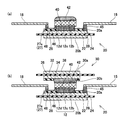
- 12 (a)-FIG. 12 (d) are cross-sectional views illustrating the first step in the method for manufacturing the semiconductor device 10.
- FIG. 12A shows a step of preparing the first insulated circuit board 20.
- FIG. 12B shows a step of forming the resin layer 50 on the first inner conductor plate 24 of the first insulating circuit board 20.
- FIG. 12A shows a step of preparing the first insulated circuit board 20.
- FIG. 12B shows a step of forming the resin layer 50 on the first inner conductor plate 24 of the first insulating circuit board 20.
- FIG. 12C shows a step of exposing the formed resin layer 50.
- FIG. 12D shows a step of developing the exposed resin layer 50.
- 13 (a)-FIG. 13 (e) are cross-sectional views illustrating a second step in the method of manufacturing the semiconductor device 10.
- FIG. 13A shows a step of forming the seed layer 52 on the first insulating layer 26 formed in the first step.
- FIG. 13B shows a step of forming a patterned resist layer 54 on the seed layer 52.
- FIG. 13C shows a step of forming the plating layer 56 on the seed layer 52 masked by the resist layer 54.
- FIG. 13D shows a step of removing the resist layer 54 from the seed layer 52.
- FIG. 13E shows a step of removing the seed layer 52.
- FIG. 14 (b) are cross-sectional views illustrating a third step in the method for manufacturing the semiconductor device 10.
- FIG. 14A shows a first reflow process.
- FIG. 14B shows a second reflow process.
- 15 (a)-FIG. 15 (c) are cross-sectional views illustrating a modified example of the second step in the method for manufacturing the semiconductor device 10.
- FIG. 15A shows a step of forming the patterned resist layer 55 on the first insulating layer 26 formed in the first step.
- FIG. 15B shows a step of forming the plating layer 57 on the first insulating layer 26 masked by the resist layer 55.
- FIG. 15C shows a step of removing the resist layer 55 from the first insulating layer 26.
- FIG. 10E It is sectional drawing which shows the internal structure of the semiconductor device 10E of the modification 5.
- This cross-sectional view shows a cross section perpendicular to the thickness direction of the semiconductor device 10E.
- This cross-sectional view shows a cross section perpendicular to the thickness direction of the semiconductor device 10F.
- FIG. It is a top view 20a of the 1st insulation circuit board 20 in Example 2.
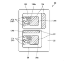
- FIG. 8 is a cross-sectional view taken along the line XXII-XXII of FIG. It is an electronic circuit diagram which shows the structure of the semiconductor device 100. It is a top view on the lower surface 30b of the 2nd insulation circuit board 30 in another embodiment of Example 2. FIG. It is a top view 20a of the 1st insulation circuit board 20 in another embodiment of Example 2. FIG. It is sectional drawing which shows the internal structure of another Embodiment of Example 2. FIG.
- the thickness of the conductor circuit pattern may be smaller than the thickness of the first conductor plate.
- the thickness of the conductor circuit pattern is small, it becomes easy to form a fine conductor circuit pattern by patterning processing such as etching.
- the semiconductor device may further include a first connection terminal electrically connected to the first conductor line.
- the first connection terminal may be joined to the first conductor line via a conductive bonding layer such as a solder layer.
- the first connection terminal may be connected to the first conductor line via a flexible and conductive connecting member such as a wire.
- a flexible connecting member for example, it is possible to allow a relative displacement between the first connecting terminal and the first conductor line due to thermal deformation.
- the connecting member such as a wire may be made of a metal material such as copper.
- the first conductor line may have one end electrically connected to the first semiconductor element and the other end electrically connected to the first connection terminal.
- the width dimension at the other end of the first conductor line may be larger than the width dimension at one end of the first conductor line. According to such a configuration, even when the size of the first semiconductor element is relatively small, the first connection terminal can be easily connected to the first conductor line.
- the at least one first conductor line described above may include two conductor lines running in parallel with each other, and each of the two conductor lines running in parallel is the first at one end. It may be electrically connected to the semiconductor element.
- the center-to-center distance at the other end of the two parallel conductor lines may be larger than the center-to-center distance at one end of the two parallel conductor lines. According to such a configuration, one end of the two conductor lines is connected to the first semiconductor element having a relatively small size, while the other end of the two conductor lines is easily connected to, for example, another member. be able to.
- the first insulating layer may have an opening that exposes the first surface of the first conductor plate, and the first electrode of the first semiconductor element passes through the opening of the first insulating layer. It may be joined to the first surface of the first conductor plate. According to such a configuration, it is possible to prevent the first electrode from being joined beyond the intended region on the first conductor plate. Therefore, it is possible to reduce the short circuit between the first electrode and the second electrode due to this joining.
- the first electrode may be the power electrode of the first semiconductor element
- the second electrode may be the signal electrode of the first semiconductor element.
- a power semiconductor element having a vertical structure can be adopted as the first semiconductor element.
- the semiconductor device may further include an insulating cover that partially covers the first conductor line.
- the first insulating layer of the first conductor plate may be provided with a mark for positioning the first semiconductor element at a position corresponding to the peripheral edge of the first semiconductor element.
- the first semiconductor element can be accurately positioned on the first conductor plate at the time of manufacturing the semiconductor device.
- the specific configuration of the mark is not particularly limited, but the mark may be configured to be identifiable by, for example, image processing.
- the semiconductor device may further include electrical components located on the first insulating layer.
- the conductor circuit pattern may further have at least one conductor line connected to the electrical component.
- any electric component can be incorporated into the semiconductor device by utilizing the surplus region on the first insulating layer.
- the electrical component may include a thermistor. According to such a configuration, the temperature of the first semiconductor element can be measured relatively accurately. For example, since it is not necessary to provide a temperature sensor on the first semiconductor element, the first semiconductor element can be made relatively small or the active region of the first semiconductor element can be increased accordingly.
- the electrical component may be a drive circuit for driving the first semiconductor element.
- the semiconductor device may further include an insulator substrate provided with a first conductor plate.
- the insulator substrate referred to in the present specification is a plate-shaped member made of an insulator.
- the insulator substrate may be constructed using, for example, a ceramic material.
- the first conductor plate and the insulator substrate may be a part of a so-called DBC (Direct Bonded Copper) substrate, a DBA (Direct Bonded Aluminum) substrate, or an AMB substrate.
- the AMB substrate referred to here broadly means an insulating circuit board manufactured by using active metal brazing (Active Metal Brazing), and examples thereof include an active metal brazing copper (Active Metal Brazing Copper) circuit board.
- the semiconductor device may further include a second conductor plate having a second surface facing the other surface of the first semiconductor element.
- the first semiconductor element may further have a third electrode provided on another surface and electrically connected to the second surface of the second conductor plate.
- the semiconductor device may further include a second insulating layer that is provided on the second surface of the second conductor plate and covers a part of the second surface.
- the semiconductor device may further include a first connection terminal electrically connected to the first conductor line.
- one end of the first connection terminal may be located between the first conductor line and the second insulating layer and may be joined to the first conductor line.
- a spacer provided integrally or separately from the first connection terminal may be arranged between one end of the first connection terminal and the second insulating layer. According to such a configuration, a spacer provided between one end of the first connection terminal and the second insulating layer allows a semiconductor between the first conductor plate and the second conductor plate without using a jig. The positioning of the devices in the stacking direction can be made accurate.
- the semiconductor device may further include a conductor film provided on the second insulating layer.
- the spacer may be bonded to the conductor membrane via a bonding layer.
- the semiconductor device further comprises a second semiconductor device having one surface provided with the fourth and fifth electrodes and another surface located on the opposite side of the fifth surface. May be good.
- the first surface of the first conductor plate may face one surface of the second semiconductor element and may be electrically connected to the fourth electrode of the second semiconductor element.
- the conductor circuit pattern may further have at least one second conductor line electrically connected to the second semiconductor device.
- at least one second conductor line may include a conductor line electrically connected to the fifth electrode.
- the semiconductor device may have two or more semiconductor elements, and the semiconductor elements may be connected in parallel with each other.
- the second conductor line may be common with at least a part of the first conductor line.
- the first conductor line may branch or merge from the middle of the second conductor line, or the second conductor line may branch or merge from the middle of the first conductor line.
- one or a plurality of conductor lines can be shared between the first semiconductor element and the second semiconductor element, and the configuration of the conductor circuit pattern is relatively simple with respect to the number of semiconductor elements. can do. This makes it possible to reduce the size of the semiconductor device, for example.
- the common conductor line may be, for example, one that transmits a common control signal (for example, a gate drive signal) to the first semiconductor element and the second semiconductor element.
- the semiconductor device further comprises a second semiconductor element, a third conductor plate, a fourth conductor plate, a third insulating layer, a joint member, and a second conductor circuit pattern. good.
- the second semiconductor element may have one surface provided with the fourth electrode and the fifth electrode, and another surface located on the opposite side of the one surface and provided with the sixth electrode.
- the third conductor plate has a third surface facing one surface of the second semiconductor element, and may be electrically connected to the fourth electrode of the second semiconductor element on the third surface.
- the fourth conductor plate has a fourth surface facing the other surface of the first semiconductor element, and may be electrically connected to the sixth electrode of the second semiconductor element on the fourth surface.
- the joint member is located between the first conductor plate and the fourth conductor plate, and the first conductor plate and the fourth conductor plate may be electrically connected to each other.
- the second conductor circuit pattern may be provided on the third insulating layer, which is provided on the third surface of the third conductor plate and covers a part of the third surface, and the third insulating layer.
- the second conductor circuit pattern may have at least one second conductor line electrically connected to the second semiconductor element, and at least one second conductor line is electrically connected to the fifth electrode. It may include connected conductor lines.
- the semiconductor device may have two or more semiconductor elements, and the semiconductor elements may be connected in series with each other.
- the semiconductor device may further include an insulator substrate provided with a first conductor plate and a third conductor plate.
- the semiconductor device may further include a second conductor plate and another insulator substrate provided with a fourth conductor plate.
- the semiconductor device 10 of the first embodiment will be described with reference to FIGS. 1 to 7.
- the semiconductor device 10 is adopted in, for example, a power control device for an electric vehicle, and can form at least a part of a power conversion circuit such as a converter or an inverter.
- the term "electric vehicle” as used herein broadly means a vehicle having a motor for driving wheels. For example, an electric vehicle charged by external electric power, a hybrid vehicle having an engine in addition to the motor, and a fuel cell-powered fuel. Including battery cars, etc.
- the semiconductor device 10 includes a first semiconductor element 12 and a sealing body 11.
- the sealing body 11 is constructed by using an insulating material.
- the encapsulant 11 can be formed using, for example, an epoxy resin.
- the sealing body 11 generally has a plate shape, and has an upper surface 11a and a lower surface 11b located on the opposite side of the upper surface 11a. Further, the sealing body 11 has a first side surface 11c, a second side surface 11d, a first end surface 11e, and a second end surface 11f, and these four surfaces are between the upper surface 11a and the lower surface 11b. It is extending.
- the first side surface 11c and the second side surface 11d are located on opposite sides of each other, and the first end surface 11e and the second end surface 11f are located on opposite sides of each other.
- the semiconductor device 10 includes a plurality of connection terminals 14, 15 and 18 whose other ends project from the sealing body 11. One end of each of the plurality of connection terminals 14, 15 and 18 is electrically connected to the first semiconductor element 12 inside the sealing body 11.
- the plurality of connection terminals 14, 15, and 18 include a first power terminal 14 and a second power terminal 15, and a plurality of first signal terminals 18.
- the first power terminal 14 and the second power terminal 15 project from the first end surface 11e of the encapsulant 11, and each first signal terminal 18 projects from the second end surface 11f of the encapsulant 11.
- the first power terminal 14 can be connected to the positive electrode of the external DC power supply, and the second power terminal 15 can be connected to the negative electrode of the external DC power supply.
- the first signal terminal 18 is connected to an external device such as a control board to control the first semiconductor element 12, for example.
- the connection terminals 14, 15 and 18 are formed by using a conductive material such as copper or another metal material.
- the first semiconductor element 12 is a power semiconductor element and has a semiconductor substrate 12a and a plurality of electrodes 12b, 12c, 12d.
- the plurality of electrodes 12b, 12c, 12d include a collector electrode 12b and an emitter electrode 12c connected to the power circuit, and a plurality of signal electrodes 12d connected to the signal circuit.
- the first semiconductor element 12 is a switching element, and can conduct and cut off between the collector electrode 12b and the emitter electrode 12c.
- the first semiconductor element 12 is a power semiconductor element having a vertical structure
- the collector electrode 12b is located on the upper surface side of the semiconductor substrate 12a
- the emitter electrode 12c and the plurality of signal electrodes 12d are It is located on the lower surface side of the semiconductor substrate 12a.
- the emitter electrode 12c and the signal electrode 12d are examples of the first electrode and the second electrode in the technique disclosed in the present specification, respectively
- the collector electrode 12b is the third electrode in the technique disclosed in the present specification. This is an example.
- the first semiconductor element 12 in this embodiment is an RC-IGBT (Reverse Conducting-Insulated Gate Bipolar Transistor). Therefore, the first semiconductor element 12 has an IGBT structure 12e and a diode structure 12f connected in parallel with the IGBT structure 12e.
- the collector electrode 12b is connected to the collector of the IGBT structure 12e
- the emitter electrode 12c is connected to the emitter of the IGBT structure 12e
- the signal electrode 12d is connected to the gate of the IGBT structure 12e.
- the collector electrode 12b is connected to the cathode of the diode structure 12f
- the emitter electrode 12c is connected to the anode of the diode structure 12f.
- the first semiconductor element 12 may have a MOSFET (Metal-Oxide-Semiconductor Field-Effect Transistor) structure.
- the first semiconductor element 12 may have a drain electrode and a source electrode instead of the collector electrode 12b and the emitter electrode 12c, the drain electrode is connected to the drain of the MOSFET structure, and the source electrode is the MOSFET. It may be connected to the source of the structure. Further, in this case, the signal electrode 12d may be connected to the gate of the MOSFET structure.
- MOSFET Metal-Oxide-Semiconductor Field-Effect Transistor
- the specific configuration of the first semiconductor element 12 is not particularly limited, and various semiconductor elements can be adopted for the first semiconductor element 12.
- the material constituting the semiconductor substrate 12a of the first semiconductor element 12 is not particularly limited, and various semiconductor materials such as silicon (Si), silicon carbide (SiC), and gallium nitride (GaN) can be adopted.
- the semiconductor device 10 includes a first insulated circuit board 20 and a second insulated circuit board 30.
- the two insulating circuit boards 20 and 30 face each other with the first semiconductor element 12 interposed therebetween.
- the first insulated circuit board 20 has an upper surface 20a located inside the sealing body 11 and a lower surface 20b located on the opposite side of the upper surface 20a.
- the first insulating circuit board 20 faces the lower surface of the first semiconductor element 12 on the upper surface 20a, and is bonded to the emitter electrode 12c of the first semiconductor element 12 via the solder layer 40.
- the second insulating circuit board 30 has a lower surface 30b located inside the sealing body 11 and an upper surface 30a located on the opposite side of the lower surface 30b.
- the second insulating circuit board 30 faces the upper surface of the first semiconductor element 12 on the lower surface 30b, and is bonded to the collector electrode 12b of the first semiconductor element 12 via the solder layer 42.
- the first insulated circuit board 20 and the second insulated circuit board 30 are electrically and thermally connected to the first semiconductor element 12 inside the encapsulant 11, and form a part of the power circuit. do.
- the first insulated circuit board 20 has a first ceramic board 22.
- the first ceramic substrate 22 is a plate-like member of an insulator made of ceramic.
- a first inner conductor plate 24 is provided on the upper surface of the first ceramic substrate 22, and a first outer conductor plate 28 is provided on the lower surface of the first ceramic substrate 22.
- the first inner conductor plate 24 and the first outer conductor plate 28 are made of a conductor material.
- the first inner conductor plate 24 and the first outer conductor plate 28 are electrically insulated by a ceramic substrate 22.
- the first inner conductor plate 24 is bonded to the emitter electrode 12c of the first semiconductor element 12 via a solder layer 40.
- the first insulating circuit board 20 is electrically connected to the emitter electrode 12c of the first semiconductor element 12 in the first inner conductor plate 24.
- the second insulated circuit board 30 has a second ceramic substrate 32.
- the second ceramic substrate 32 is a plate-like member of an insulator made of ceramic.
- a second outer conductor plate 38 is provided on the upper surface of the second ceramic substrate 32, and a second inner conductor plate 34 is provided on the lower surface of the second ceramic substrate 32.
- the second inner conductor plate 34 and the second outer conductor plate 38 are made of a conductor material.
- the second inner conductor plate 34 and the second outer conductor plate 38 are electrically insulated by the second ceramic substrate 32.
- the second inner conductor plate 34 is bonded to the collector electrode 12b of the first semiconductor element 12 via the solder layer 42.
- the second insulating circuit board 30 is electrically connected to the collector electrode 12b of the first semiconductor element 12 in the second inner conductor plate 34.
- the upper surface 30a of the second insulated circuit board 30 (that is, the second outer conductor plate 38) is exposed on the upper surface 11a of the sealing body 11, and the lower surface 20b of the first insulated circuit board 20 (that is, the first one).
- the outer conductor plate 28) is exposed on the lower surface 11b of the sealing body 11.
- the two insulating circuit boards 20 and 30 also function as heat radiating plates that dissipate heat generated by the first semiconductor element 12 on both sides 11a and 11b of the sealing body 11.
- a second insulating layer 36 is provided on the second inner conductor plate 34 of the second insulating circuit board 30.
- the second insulating layer 36 covers a part of the second inner conductor plate 34.
- the second insulating layer 36 has an opening 36a that exposes the second inner conductor plate 34. Therefore, the collector electrode 12b of the first semiconductor element 12 is joined to the second inner conductor plate 34 via the solder layer 42 through the opening 36a of the second insulating layer 36. Further, one end of the first power terminal 14 is joined to the second inner conductor plate 34 via the solder layer 44.
- the second insulating layer 36 may be provided on the second inner conductor plate 34 in a portion other than the joint region.
- a first insulating layer 26 is provided on the first inner conductor plate 24 of the first insulating circuit board 20.
- the first insulating layer 26 covers a part of the first inner conductor plate 24.
- the first insulating layer 26 has an opening 26a that exposes the first inner conductor plate 24.
- the emitter electrode 12c of the first semiconductor element 12 is joined to the first inner conductor plate 24 via the solder layer 40 through the opening 26a of the first insulating layer 26.
- one end of the second power terminal 15 is joined to the first inner conductor plate 24 via the solder layer 45.
- the first insulating layer 26 may be provided on the first inner conductor plate 24 in a portion other than the joint region.
- the first insulating layer 26 and the second insulating layer 36 described above are made of a material having an insulating property, and are made of a resin material such as polyimide.
- the first insulated circuit board 20 further has a first conductor circuit pattern 27.
- the first conductor circuit pattern 27 is provided on the first insulating layer 26. Although not particularly limited, the conductor circuit pattern is located inside the encapsulant 11. Further, the first conductor circuit pattern 27 includes a plurality of first conductor lines 27a. The plurality of first conductor lines 27a are electrically connected to the first semiconductor element 12. Each first conductor line 27a has an end portion close to the first semiconductor element and an other end portion away from the first semiconductor element 12. One end of the first conductor line 27a is joined to the signal electrode 12d of the first semiconductor element 12 via the solder layer 46. The other end of the first conductor line 27a is joined to one end of the first signal terminal 18 via a solder layer 48. Therefore, each of the first signal terminals 18 is electrically connected to the signal electrode 12d of the first semiconductor element 12 via the first conductor line 27a.
- the thickness t2 of the first conductor circuit pattern 27 is smaller than the thickness t1 of the first inner conductor plate 24 of the first insulating circuit board 20.
- the first conductor circuit pattern 27 is made of a conductor material such as copper or other metal material.
- the distance between the signal electrode 12d and the first conductor line 27a, and between the first conductor line 27a and the first signal terminal 18, is not limited to the solder layers 46 and 48, and has conductivity. It may be bonded through the bonding layer of.
- the first semiconductor element 12 in order to position the first semiconductor element 12 on the first insulating layer 26 of the first insulating circuit board 20 at a position corresponding to the peripheral edge of the first semiconductor element 12.
- Mark M is provided. According to such a configuration, the first semiconductor element 12 can be accurately positioned on the first inner conductor plate 24 at the time of manufacturing the semiconductor device 10.
- the specific configuration of the mark is not particularly limited, but the mark M may be configured to be identifiable by, for example, image processing.
- the first insulated circuit board 20 and the second insulated circuit board 30 are DBC boards.
- the first insulated circuit board 20 and the second insulated circuit board 30 are not limited to the DBC substrate, and may be a DBA substrate or an AMB substrate.
- each of the ceramic substrates 22 and 32 is an insulator member made of ceramic as described above.
- Each of the ceramic substrates 22 and 32 is made of a ceramic material such as aluminum oxide, silicon nitride, or aluminum nitride.
- the ceramic substrates 22 and 32 are examples of insulator substrates in the technology disclosed in the present specification.
- the insulator substrate is not limited to the ceramic material, and may be made of an insulating material such as a resin material.
- the first conductor circuit pattern 27 is provided on the first inner conductor plate 24 via the first insulating layer 26.
- the emitter electrode 12c of the first semiconductor element 12 is electrically connected to the first inner conductor plate 24, and each of the plurality of signal electrodes 12d of the first semiconductor element 12 has a first conductor circuit pattern 27. It is electrically connected to the first conductor line 27a.
- the first inner conductor plate 24 electrically connected to the emitter electrode 12c and the first conductor line 27a electrically connected to the signal electrode 12d are interposed between them. It is insulated by the first insulating layer 26.
- the thickness t2 of the first conductor circuit pattern 27 is smaller than the thickness t1 of the first inner conductor plate 24.
- the thickness t2 of the first conductor circuit pattern 27 is small, it becomes easy to form a fine first conductor circuit pattern 27 by patterning processing such as etching.
- the voltage applied to the first conductor circuit pattern 27 is the first inner conductor plate which is a part of the power circuit. It becomes smaller than the voltage applied to 24. Therefore, the thickness t2 of the first conductor circuit pattern 27 can be made relatively small by that amount.
- the thickness t2 of the conductor circuit pattern may be several tens of micrometers.
- the signal electrode 12d of the first semiconductor element 12 is an example of the second electrode disclosed in the present specification, and the second electrode may be, for example, a collector electrode of a power electrode.
- the first semiconductor element 12 may be a power semiconductor element having a horizontal structure.
- the first insulating layer 26 has an opening 26a that exposes the upper surface 20a (that is, the first inner conductor plate 24) of the first insulating circuit board 20.
- the emitter electrode 12c of the first semiconductor element 12 is bonded to the upper surface 20a of the first inner conductor plate 24 via the opening 26a of the first insulating layer 26 via the solder layer 40. According to such a configuration, it is possible to prevent the emitter electrode 12c from being joined beyond the intended region on the first inner conductor plate 24. Therefore, it is possible to reduce short-circuiting between the emitter electrode 12c and each of the plurality of signal electrodes 12d due to this bonding.
- the first inner conductor plate 24 and the emitter electrode 12c are not limited to the solder layer 40, and may be bonded via another bonding layer having conductivity.
- the semiconductor device 10 of the present embodiment includes a second insulating layer 36 provided on the lower surface 30b (that is, the second inner conductor plate 34) of the second insulating circuit board 30 and covering a part of the lower surface 30b. ing. According to such a configuration, it is possible to prevent the second inner conductor plate 34 from being unintentionally short-circuited with the first inner conductor plate 24 or other members of the first insulating circuit board 20. That is, a short circuit between the collector and the emitter of the semiconductor device 10 is prevented.
- the first conductor line 27a is electrically connected to one end portion electrically connected to the first semiconductor element 12 and to the first signal terminal 18. It has the other end.
- the width dimension w2 at the other end of the first conductor line 27a may be larger than the width dimension w1 at one end of the first conductor line 27a. According to such a configuration, even when the size of the first semiconductor element 12, particularly the width dimension of the signal electrode 12d, is relatively small, for example, the first signal terminal 18 having a width dimension larger than that of the first signal electrode 12d is first. It can be easily connected to the conductor line 27a.
- the distance d2 is larger than the distance d1 between the centers at one end of two parallel first conductor lines 27a.
- the semiconductor device 10 of this embodiment can be deformed in various ways. Other modifications will be described with reference to FIGS. 8-11.
- Modification Example 1 The semiconductor device 10A of Modification 1 will be described with reference to FIG. As shown in FIG. 8, in the semiconductor device 10A of the first modification, the first signal terminal 18 is connected to the first conductor line 27a via a wire 49 instead of the solder layer 48 in the first embodiment. In the semiconductor device 10A of the first modification, the parts other than the wire 49 can be configured in the same manner as the semiconductor device 10 of the first embodiment. In the first modification, the same components as those in the first embodiment are displayed with the same reference numbers, and duplicate description will be omitted.
- the wire 49 connects the first signal terminal 18 and the first conductor line 27a, and is made of a metal material such as copper.
- the connecting member connecting the first signal terminal 18 and the first conductor line 27a is not limited to the wire 49, and may be, for example, a connecting member having flexibility and conductivity. By using the wire 49 having such flexibility, it is possible to allow a relative displacement between the first signal terminal 18 and the first conductor line 27a due to, for example, thermal deformation. Not only between the first signal terminal 18 and the first conductor line 27a, but also between the first conductor line 27a and the signal electrode 12d may be connected via, for example, a wire.
- Modification 2 The semiconductor device 10B of Modification 2 will be described with reference to FIG.
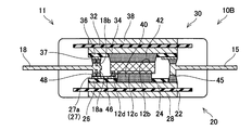
- the semiconductor device 10B of the second modification includes a conductor film 37 in addition to the configuration of the semiconductor device 10 of the first embodiment. Further, the shapes of the first signal terminal 18 and the second power terminal 15 in the first embodiment have been partially changed.
- other parts other than these parts can be configured in the same manner as the semiconductor device 10 of the first embodiment.
- the same components as those in the first embodiment are displayed with the same reference numbers, and duplicate description will be omitted.
- the conductor film 37 is provided on the second insulating layer 36 of the second insulating circuit board 30.
- the conductor film 37 is made of a conductor material such as copper or other metal material.
- a plurality of first convex portions 18a extending toward the first conductor line 27a are provided.
- the first signal terminal 18 is joined to the other end of the first conductor line 27a at each of the first convex portions 18a via the solder layer 48.
- each first signal terminal 18 a plurality of second convex portions 18b extending toward the conductor film 37 are provided at positions opposite to the plurality of first convex portions 18a. ing.
- the first signal terminal 18 is joined to the conductor film 37 via a solder layer at each of the second convex portions 18b.
- the first signal terminal 18 is fixed to the first insulating circuit board 20 via the first convex portion 18a
- the first signal terminal 18 is fixed to the first insulating circuit board 20 via the first convex portion 18a and the second insulating circuit board 30 via the second convex portion 18b. Is fixed to. Therefore, changes in the relative positions and orientations of the first insulated circuit board 20 and the second insulated circuit board 30 of the first signal terminal 18 are suppressed.
- a third convex portion 15a extending toward the first inner conductor plate 24 is provided at one end of the second power terminal 15, and the third convex portion 15a is provided.
- a fourth convex portion 15b that is located on the opposite side of the conductor film 37 and extends toward the conductor film 37 is provided.
- the second power terminal 15 is joined to the first inner conductor plate 24 via the solder layer 45 at the third convex portion 15a, and is joined to the conductor film 37 via the solder layer at the fourth convex portion 15b. Be joined.
- the semiconductor device 10B has a plurality of convex portions 18a, 18b, 15a, and 15b of the first insulated circuit board 20 and the second insulated circuit board 30 at both the first signal terminal 18 and the second power terminal 15. Can be fixed via.
- the first insulated circuit board 20 and the second insulated circuit board 30 can be stably supported. Therefore, even when the semiconductor device 10B is assembled, the positioning of the semiconductor device 10B between the insulating circuit board 20 and the second insulating circuit board 30 in the stacking direction can be accurately performed without using a jig.
- the number of convex portions 18a, 18b, 15a, 15b in the first signal terminal 18 and the second power terminal 15 is not limited to the number shown in FIG.
- Each of the first signal terminal 18 and the second power terminal 15 may be provided with one or more convex portions 18a, 18b, 15a, 15b.
- each of the convex portions 18a, 18b, 15a, and 15b is integrally formed with the first signal terminal 18 or the second power terminal 15, but the first signal terminal 18 is not limited thereto.
- it may be provided as a member (for example, a spacer) separate from the second power terminal 15.
- the spacer may be formed using the same or different material as the first signal terminal 18 or the second power terminal 15.
- the second convex portion 18b and / or the fourth convex portion 15b may be formed integrally with the second insulating layer 36 or may be formed separately.
- the semiconductor device 10B of the modified example 2 does not have to include the second insulating layer 36.
- the convex portions 18a, 18b, 15a, 15b may be provided in all of the plurality of connection terminals 14, 15, 18 or at least one of the plurality of connection terminals 14, 15, 18. It may have been.
- the semiconductor device 10C of Modification 3 includes an insulating cover 29 in addition to the configuration of the semiconductor device 10 of the first embodiment.
- the parts other than the insulating cover 29 can be configured in the same manner as the semiconductor device 10 of the first embodiment.
- the same components as those in the first embodiment are displayed with the same reference numbers, and duplicate description will be omitted.
- the insulating cover 29 is provided on the first conductor line 27a of the first insulating circuit board 20. The insulating cover 29 partially covers the first conductor line 27a.
- the insulating cover 29 is made of a material having an insulating property, and can be made of a resin material such as polyimide. According to such a configuration, it is possible to prevent the first conductor line 27a from being unintentionally short-circuited with another member.
- the semiconductor device 10D of Modification 4 will be described with reference to FIG.
- the semiconductor device 10D of the modified example 4 is a ceramic substrate 22, 32 instead of the first insulated circuit board 20 and the second insulated circuit board 30 as compared with the semiconductor device 10 of the first embodiment.
- the first conductor plate 25 and the second conductor plate 35 are provided.
- the first conductor plate 25 corresponds to the one in which the first inner conductor plate 24 and the first outer conductor plate 28 in the first embodiment are integrated.
- the second conductor plate 35 corresponds to the one in which the second inner conductor plate 34 and the second outer conductor plate 38 in the first embodiment are integrated.
- the semiconductor device 10D of the modified example 4 can be configured in the same manner as the semiconductor device 10 of the first embodiment except that the ceramic substrates 22 and 32 are not provided.
- the same components as those in the first embodiment are displayed with the same reference numbers, and duplicate description will be omitted. Even with such a configuration, between the first conductor plate 25 electrically connected to the emitter electrode 12c and the first conductor line 27a electrically connected to the signal electrode 12d, between them. It is insulated by an intervening first insulating layer 26. This prevents unintended contact between the first conductor plate 25 and the first conductor line 27a.
- the manufacturing method is roughly divided into the following three steps.
- the three steps are a first step of forming the first insulating layer 26 on the first inner conductor plate 24 of the first insulating circuit board 20, and a second step of forming the first conductor line 27a on the first insulating layer 26.
- the steps other than those described here can be manufactured by using known techniques.
- the first step will be described with reference to FIGS. 12 (a) and 12 (d).
- the first insulated circuit board 20 is prepared.
- the resin layer 50 is formed on the upper surface 20a of the prepared first insulating circuit board 20 (that is, the first inner conductor plate 24).
- the resin layer 50 is made of a photosensitive resin material, and is formed by using a resin material such as polyimide.
- the formed resin layer 50 is exposed. Specifically, the surface of the resin layer 50 is irradiated with light through the photomask P to expose a predetermined range of the resin layer 50.
- the exposed resin layer 50 is developed.
- an unnecessary portion of the exposed resin layer 50 (a portion serving as a bonding region such as the inside of the opening 26a of the first insulating layer 26) is removed and washed. As a result, the first insulating layer 26 is formed on the first insulating circuit board 20.
- the seed layer 52 is formed on the first insulating layer 26 formed in the first step.
- the seed layer 52 is formed by, for example, a sputtering method.
- the seed layer 52 is constructed using a conductor material such as copper or another metal material.
- the thickness dimension of the seed layer 52 may be about 0.1-5 micrometers.
- a patterned resist layer 54 is formed on the seed layer 52. Specifically, after forming the resist layer, the exposed resist layer is removed by exposure and development processing. As a result, the patterned resist layer 54 is formed. Therefore, the seed layer 52 is masked by the patterned resist layer 54.
- the plating layer 56 is formed on the seed layer 52 masked by the resist layer 54.
- the plating layer 56 is formed by a plating process.
- the resist layer 54 is removed from the seed layer 52.
- the resist layer 54 is decomposed and removed by, for example, an ashing treatment.
- the seed layer 52 other than the seed layer 52 formed under the plating layer 56 is removed.
- the seed layer 52 is removed by, for example, a dry etching method.
- the first conductor line 27a is provided on the first insulating layer 26.
- a second insulating circuit board 30, a first semiconductor element 12, and a plurality of connection terminals 15 and 18 are prepared.
- the illustration of the first power terminal 14 is omitted.
- the first semiconductor element 12 and the plurality of connection terminals 15 and 18 may be prepared as one member (for example, a lead frame) integrally formed with the first semiconductor element 12.
- the second insulated circuit board 30 can be produced with reference to the first step of the first insulated circuit board 20, and the description of the manufacturing method thereof is omitted.
- the first reflow step is carried out.
- the first semiconductor element 12 and the plurality of connection terminals 15 and 18 are soldered at predetermined positions on the upper surface 20a of the first insulating circuit board 20 provided with the first conductor line 27a in the second step. Attach. Specifically, the emitter electrode 12c of the first semiconductor element 12 is bonded to the first inner conductor plate 24 of the first insulating circuit board 20 via the solder layer 40, and the first signal electrode 12d of the first semiconductor element 12 Is joined to one end of the first conductor line 27a of the first insulating circuit board 20 via the solder layer 46.
- the second reflow step is carried out.
- the second insulating circuit board 30 is soldered to the lower surface of the first semiconductor element 12.
- the second inner conductor plate 34 of the second insulating circuit board 30 is joined to the collector electrode 12b of the first semiconductor element 12 via the solder layer 42.
- the semiconductor device 10 can be manufactured by the above manufacturing method. However, the manufacturing method of the semiconductor device 10 is not limited to the above-mentioned method. The second step of the semiconductor device 10 illustrated in FIGS. 13 (a) to 13 (e) may be replaced with another method. Other manufacturing methods will be described below with reference to FIGS. 15 (a)-(c).
- a patterned resist layer 55 is formed on the first insulating layer 26 formed in the first step. Specifically, after forming the resist layer, the exposed resist layer is removed by exposure and development processing. As a result, the patterned resist layer 55 is formed. Therefore, the first insulating layer 26 is masked by the patterned resist layer 55.
- the plating layer 57 is formed on the first insulating layer 26 masked by the resist layer 55.
- the plating layer 57 is formed by a plating process.
- the resist layer 55 is removed from the first insulating layer 26.
- the resist layer 55 is decomposed and removed by, for example, an ashing treatment. In this ashing treatment, it is required to sufficiently remove the resist layer 55 while leaving the first insulating layer 26 remaining. Therefore, as the ashing solution used for the ashing treatment, it is preferable to select a solution that reacts well with the material constituting the resist layer 55 and does not react with the material constituting the first insulating layer 26, is difficult to react, or reacts relatively slowly. ..
- the method for manufacturing the semiconductor device 10 described above can be applied to the modified examples 5 and 6 described later in addition to the modified examples 1-4 described above.
- the semiconductor device 10E of Modification 5 will be described with reference to FIG. As shown in FIG. 16, the semiconductor device 10E of the modified example 5 further includes a second semiconductor element 13 in addition to the configuration of the semiconductor device 10 of the first embodiment. Along with this change, the configuration of the first conductor circuit pattern 27 of the first insulating circuit board 20 is partially changed, and the first conductor circuit pattern 27 further has a second conductor line 27b. In the semiconductor device 10E of the modified example 5, the parts other than the second semiconductor element 13 and the second conductor line 27b can be configured in the same manner as the semiconductor device 10 of the first embodiment. In the fifth modification, the same components as those in the first embodiment are displayed with the same reference numbers, and duplicate description will be omitted.
- the second semiconductor element 13 is a power semiconductor element and can be configured in the same manner as the first semiconductor element 12, and the second semiconductor element 13 includes a semiconductor substrate and a plurality of electrodes 13c and 13d.
- the plurality of electrodes 13c and 13d include a collector electrode and an emitter electrode 13c connected to the power circuit, and a plurality of signal electrodes 13d connected to the signal circuit.
- the second semiconductor element 13 is a switching element, and can conduct and cut off between the collector electrode and the emitter electrode 13c.
- the collector electrode is located on the upper surface side of the semiconductor substrate, and the emitter electrode 13c and the plurality of signal electrodes 13d are located on the lower surface side of the semiconductor substrate.
- the first insulated circuit board 20 and the second insulated circuit board 30 face each other with the first semiconductor element 12 and the second semiconductor element 13 interposed therebetween.
- the first insulating circuit board 20 faces the lower surfaces of the first semiconductor element 12 and the second semiconductor element 13 on the upper surface 20a. Therefore, the first inner conductor plate 24 of the first insulating circuit board 20 is bonded to the emitter electrode 12c of the first semiconductor element 12 and to the emitter electrode 13c of the second semiconductor element 13.
- the second insulating circuit board 30 faces the upper surfaces of the first semiconductor element 12 and the second semiconductor element 13 on the lower surface 30b.
- the second inner conductor plate 34 of the second insulating circuit board 30 is bonded to the collector electrode 12b of the first semiconductor element 12 and to the collector electrode of the second semiconductor element 13. As a result, the first semiconductor element 12 and the second semiconductor element 13 are connected in parallel.
- first conductor circuit pattern 27 of the first insulating circuit board 20 further includes a second conductor line 27b in addition to the plurality of first conductor lines 27a.
- the second conductor line 27b is electrically connected to the second semiconductor element 13.
- the second conductor line 27b has one end portion close to the second semiconductor element 13 and the other end portion away from the second semiconductor element 13.
- One end of the second conductor line 27b is joined to the second semiconductor element 13, and the other end of the second conductor line 27b is joined to one end of the first signal terminal 18.
- first inner conductor plate 24 electrically connected to the emitter electrode 12c of the first semiconductor element 12 and the first conductor line 27a electrically connected to the signal electrode 12d.
- Insulated by a first insulating layer 26 interposed between them. This prevents unintended contact between the first inner conductor plate 24 and the first conductor line 27a.
- the first inner conductor plate 24 electrically connected to the emitter electrode 13c of the second semiconductor element 13 and the second conductor line 27b electrically connected to the signal electrode 13d are interposed between them. It is insulated by the first insulating layer 26. This prevents unintended contact between the first inner conductor plate 24 and the second conductor line 27b.
- the second conductor line 27b in the modified example 5 is common with a part of the first conductor line 27a.
- one or a plurality of conductor lines can be shared between the first semiconductor element 12 and the second semiconductor element 13, and the conductor circuit pattern can be configured with respect to the number of the semiconductor elements 12 and 13. It can be relatively simple. Thereby, for example, the semiconductor device 10E can be miniaturized.
- the common conductor line may be, for example, one that transmits a common control signal (for example, a gate drive signal) to the first semiconductor element 12 and the second semiconductor element 13.
- the other end of the first conductor line 27a and the other end of the second conductor line 27b are shared.
- the structure in which the first conductor line 27a and the second conductor line 27b are shared is not limited to this. At least a part of the second conductor line 27b may be common to at least a part of the first conductor line 27a.
- the semiconductor device 10F of Modification 6 will be described with reference to FIG.
- the semiconductor device 10E of the modification 6 includes a thermistor 60 and a second signal terminal 19 electrically connected to the thermistor 60, in addition to the configuration of the semiconductor device 10E of the modification 5.
- the configuration of the conductor circuit pattern of the first insulating circuit board 20 is partially changed.
- the conductor circuit pattern further has a plurality of third conductor lines 27c.
- the parts other than the second signal terminal 19 and the third conductor line 27c can be configured in the same manner as the semiconductor device 10 of the modification 5.
- the same components as the modified example 5 are displayed with the same reference numbers, and duplicate description will be omitted.
- the semiconductor device 10F of the modification 6 includes a thermistor 60.
- the thermistor 60 measures the temperatures of the semiconductor elements 12 and 13 by passing a current through the thermistor 60 and measuring the resistance values of both ends 60a and 60b of the thermistor 60.
- the conductor circuit pattern of the first insulating circuit board 20 has a plurality of (here, two) third conductor lines 27c. Each third conductor line 27c is electrically insulated from the first semiconductor element 12 and the second semiconductor element 13. One end of the third conductor line 27c is connected to one end 60a of the thermistor, and one end of the other third conductor line 27c is connected to the other end 60b of the thermistor 60.
- the semiconductor device 10E includes a plurality of second signal terminals 19.
- the other end of one third conductor line 27c is connected to the second signal terminal 19, and the other end of the other third conductor line 27c is connected to the second signal terminal 19. Therefore, each second signal terminal 19 is electrically connected to the thermistor 60 via a third conductor line 27c.
- the semiconductor device 10F the average temperature of the two semiconductor elements 12 and 13 can be measured relatively accurately. For example, since it is not necessary to provide a temperature sensor on each of the semiconductor elements 12 and 13, the respective semiconductor elements 12 and 13 can be made relatively small, or the active region of each of the semiconductor elements 12 and 13 can be increased accordingly. You can also do it.
- the thermistor 60 is an example of an electric component in the technology disclosed in the present specification. Therefore, the semiconductor device 10F may include other electrical components in place of or in addition to the thermistor 60. According to such a configuration, any electric component can be incorporated into the semiconductor device 10F by utilizing the surplus region on the first insulating layer 26. Further, as another embodiment, the electric component may be a drive circuit for driving each semiconductor element 12.
- Example 2 The semiconductor device 100 of the second embodiment will be described with reference to FIGS. 18 to 23.
- the semiconductor device 100 has a second semiconductor element 113, a joint member 158, and a plurality of connection terminals 14, 15, 116, 18 as compared with the semiconductor device 10 of the first embodiment. 119 and 119 are further provided.
- a part of the configurations of the first insulated circuit board 20 and the second insulated circuit board 30 has also been changed.
- other parts other than the above-mentioned components can be configured in the same manner as the semiconductor device 10 of the first embodiment.
- the same components as those in the first embodiment are displayed with the same reference numbers, and duplicate description will be omitted.
- the semiconductor device 100 includes a plurality of connection terminals 14, 15, 116, 18, and 119 whose other ends project from the sealing body 11.
- One end of each of the plurality of connection terminals 14, 15, 116, 18, and 119 is electrically connected to the first semiconductor element 12 or the second semiconductor element 113 inside the sealing body 11.
- the plurality of connection terminals 14, 15, 116, 18 and 119 include a first power terminal 14, a second power terminal 15 and a third power terminal 116, and a plurality of first signal terminals 18 and a plurality of second signal terminals 119. including.
- the first power terminal 14 and the second power terminal 15 project from the first end surface 11e of the sealant 11, and the third power terminal 116 and the respective first signal terminals 18 and second signal terminals 119 are sealed.
- the first power terminal 14 can be connected to the positive electrode of the external DC power supply, and the second power terminal 15 can be connected to the negative electrode of the external DC power supply.
- the third power terminal 116 can be connected to a load connected to the power circuit.
- the first signal terminal 18 and the second signal terminal 119 are connected to an external device such as a control board for controlling the first semiconductor element 12 and the second semiconductor element 113, for example.
- the second semiconductor element 113 can be configured in the same manner as the first semiconductor element 12.
- the second semiconductor element 113 includes a semiconductor substrate 113a and a plurality of electrodes 113b, 113c, 113d.
- the plurality of electrodes 113b, 113c, 113d include a collector electrode 113b and an emitter electrode 113c connected to the power circuit, and a plurality of signal electrodes 113d connected to the signal circuit.
- the collector electrode 113b is located on the upper surface side of the semiconductor substrate 113a, and the emitter electrode 113c and the plurality of signal electrodes 113d are located on the lower surface side of the semiconductor substrate 113a.
- the second semiconductor element 113 is an RC-IGBT, and the second semiconductor element 113 has an IGBT structure 113e and a diode structure 113f connected in parallel with the IGBT structure 113e.
- the emitter electrode 113c and the signal electrode 113d are examples of the fourth electrode and the fifth electrode in the technique disclosed in the present specification, respectively, and the collector electrode 113b is the sixth electrode in the technique disclosed in the present specification. This is an example.
- the first insulated circuit board 20 and the second insulated circuit board 30 face each other with the first semiconductor element 12 and the second semiconductor element 113 interposed therebetween.
- the first insulating circuit board 20 faces the lower surface of the second semiconductor element 113 on the upper surface 20a, and is bonded to the emitter electrode 113c of the second semiconductor element 113 via the solder layer 180.
- the second insulating circuit board 30 faces the upper surface of the second semiconductor element 113 on the lower surface 30b, and is bonded to the collector electrode 113b of the second semiconductor element 113 via the solder layer 182.
- the first insulated circuit board 20 and the second insulated circuit board 30 are electrically and thermally connected to the first semiconductor element 12 and the second semiconductor element 113 inside the encapsulant 11, and the power is increased. It constitutes a part of the circuit.
- a third inner conductor plate 164 is provided on the upper surface of the first ceramic substrate 22 in addition to the first inner conductor plate 24, and a first one is provided on the lower surface of the first ceramic substrate 22.
- a third outer conductor plate 168 is provided in addition to the outer conductor plate 28 .
- the third inner conductor plate 164 and the third outer conductor plate 168 are made of a conductor material.
- the third inner conductor plate 164 and the third outer conductor plate 168 are electrically insulated by a ceramic substrate 22. Further, the third inner conductor plate 164 is electrically insulated from the adjacent first inner conductor plate 24 on the first ceramic substrate 22.
- the third inner conductor plate 164 is bonded to the emitter electrode 113c of the second semiconductor element 113 via the solder layer 180. As a result, the first insulating circuit board 20 is electrically connected to the emitter electrode 113c of the second semiconductor element 113 in the third inner conductor plate 164.
- a fourth outer conductor plate 178 is provided on the upper surface of the second ceramic substrate 32 in addition to the second outer conductor plate 38, and a second inner conductor plate 34 is provided on the lower surface of the second ceramic substrate 32.
- a fourth inner conductor plate 174 is provided.
- the fourth inner conductor plate 174 and the fourth outer conductor plate 178 are made of a conductor material.
- the fourth inner conductor plate 174 and the fourth outer conductor plate 178 are electrically insulated by the second ceramic substrate 32.
- the fourth inner conductor plate 174 is electrically insulated from the adjacent second inner conductor plate 34 on the second ceramic substrate 32.
- the fourth inner conductor plate 174 is bonded to the collector electrode 113b of the second semiconductor element 113 via the solder layer 182.
- the second insulating circuit board 30 is electrically connected to the collector electrode 113b of the second semiconductor element 113 in the fourth inner conductor plate 174.
- the semiconductor device 100 further includes a joint member 158.
- the joint member 158 is interposed between the first semiconductor element 12 and the second semiconductor element 113.
- the joint member 158 electrically connects the first inner conductor plate 24 and the fourth inner conductor plate 174.
- the first semiconductor element 12 and the second semiconductor element 113 are connected in series.
- the joint member 158 of the present embodiment has a first portion 158a joined to the first inner conductor plate 24 and a second portion 158b joined to the fourth inner conductor plate 174.
- the first portion 158a of the joint member 158 is joined to the first inner conductor plate 24 via the solder layer 184.
- the second portion 158b of the joint member 158 is joined to the fourth inner conductor plate 174 via the solder layer 186.
- the joint member 158 is formed as a member integrated with the third power terminal 116.
- the space between the joint member 158 and the first inner conductor plate 24 and between the joint member 158 and the fourth inner conductor plate 174 is not limited to the solder layers 184 and 186, and other conductive joint layers may be provided. It may be joined through.
- a fourth insulating layer 176 is provided on the fourth inner conductor plate 174 of the second insulating circuit board 30.
- the fourth insulating layer 176 covers a part of the fourth inner conductor plate 174.
- the fourth insulating layer 176 has two openings 176a and 176b that expose the fourth insulating layer 176 of the second insulating circuit board 30.
- the collector electrode 113b of the second semiconductor element 113 is joined to the fourth inner conductor plate 174 via the solder layer 182 through one opening 176a of the fourth insulating layer 176.
- the second portion 158b of the joint member 158 is joined to the fourth inner conductor plate 174 via the solder layer 186 through the other opening 176b of the fourth insulating layer 176.
- one end of the first power terminal 14 is joined to the second inner conductor plate 34 of the second insulating circuit board 30 via the solder layer 144.
- a second insulating layer 36 or a fourth insulating layer 176 may be provided on the second inner conductor plate 34 and the fourth inner conductor plate 174 in a portion other than the joint region.
- a third insulating layer 166 is provided on the third inner conductor plate 164 of the first insulating circuit board 20.
- the third insulating layer 166 covers a part of the third inner conductor plate 164.
- the third insulating layer 166 has an opening 166a that exposes the third inner conductor plate 164.
- the emitter electrode 113c of the second semiconductor element 113 is joined to the third inner conductor plate 164 via the solder layer 180 through the opening 166a of the third insulating layer 166.
- One end of the second power terminal 15 is joined to the third inner conductor plate 164 via the solder layer 145.
- the first insulating layer 26 also has another opening 126b that exposes the first inner conductor plate 24.
- the first portion 158a of the joint member 158 is joined to the first inner conductor plate 24 via the solder layer 184 through the other opening 126b of the first insulating layer 26.
- the first insulating layer 26 or the third insulating layer 166 may be provided on the first inner conductor plate 24 and the third inner conductor plate 164 in a portion other than the joint region.
- the third insulating layer 166 and the fourth insulating layer 176 described above are made of a material having an insulating property, and are made of a resin material such as polyimide.
- the first insulated circuit board 20 further has a second conductor circuit pattern 167.
- the second conductor circuit pattern 167 is provided on the third insulating layer 166.
- the second conductor circuit pattern 167 is located inside the sealing body 11.
- the second conductor circuit pattern 167 includes a plurality of second conductor lines 167a.
- the plurality of second conductor lines 167a are electrically connected to the second semiconductor element 113.
- Each second conductor line 167a has one end near the second semiconductor element 113 and the other end away from the second semiconductor element 113.
- One end of the second conductor line 167a is joined to the signal electrode 113d of the second semiconductor element 113 via a solder layer.
- each of the second signal terminals 119 is electrically connected to the signal electrode 113d of the second semiconductor element 113 via the second conductor line 167a.
- the second conductor circuit pattern 167 is also provided on the third inner conductor plate 164 via the third insulating layer 166.
- the emitter electrode 113c of the second semiconductor element 113 is electrically connected to the third inner conductor plate 164, and each of the plurality of signal electrodes 113d of the second semiconductor element 113 has a second conductor circuit pattern 167. It is electrically connected to the second conductor line 167a.
- the semiconductor device 100 of the second embodiment is not limited to the structure shown in FIG. 22.
- the joint member 158 may be formed as a separate member from the third power terminal 116.
- the third power terminal 116 may protrude from the first end surface 11e of the encapsulant 11, similarly to the first power terminal 14 and the second power terminal 15. Further, the third power terminal 116 may be joined to the fourth inner conductor plate 174 via the solder layer 188.
Landscapes
- Internal Circuitry In Semiconductor Integrated Circuit Devices (AREA)
- Physics & Mathematics (AREA)
- Geometry (AREA)
- Structures Or Materials For Encapsulating Or Coating Semiconductor Devices Or Solid State Devices (AREA)
Priority Applications (5)
| Application Number | Priority Date | Filing Date | Title |
|---|---|---|---|
| CN202080096322.4A CN115244689B (zh) | 2020-02-14 | 2020-02-14 | 半导体装置 |
| PCT/JP2020/005878 WO2021161526A1 (ja) | 2020-02-14 | 2020-02-14 | 半導体装置 |
| JP2022500192A JP7173396B2 (ja) | 2020-02-14 | 2020-02-14 | 半導体装置 |
| CN202510993537.0A CN120857587A (zh) | 2020-02-14 | 2020-02-14 | 半导体装置 |
| US17/886,857 US12581969B2 (en) | 2020-02-14 | 2022-08-12 | Semiconductor device |
Applications Claiming Priority (1)
| Application Number | Priority Date | Filing Date | Title |
|---|---|---|---|
| PCT/JP2020/005878 WO2021161526A1 (ja) | 2020-02-14 | 2020-02-14 | 半導体装置 |
Related Child Applications (1)
| Application Number | Title | Priority Date | Filing Date |
|---|---|---|---|
| US17/886,857 Continuation US12581969B2 (en) | 2020-02-14 | 2022-08-12 | Semiconductor device |
Publications (1)
| Publication Number | Publication Date |
|---|---|
| WO2021161526A1 true WO2021161526A1 (ja) | 2021-08-19 |
Family
ID=77291626
Family Applications (1)
| Application Number | Title | Priority Date | Filing Date |
|---|---|---|---|
| PCT/JP2020/005878 Ceased WO2021161526A1 (ja) | 2020-02-14 | 2020-02-14 | 半導体装置 |
Country Status (4)
| Country | Link |
|---|---|
| US (1) | US12581969B2 (https=) |
| JP (1) | JP7173396B2 (https=) |
| CN (2) | CN115244689B (https=) |
| WO (1) | WO2021161526A1 (https=) |
Families Citing this family (1)
| Publication number | Priority date | Publication date | Assignee | Title |
|---|---|---|---|---|
| CN116230666B (zh) * | 2023-05-05 | 2023-08-08 | 烟台台芯电子科技有限公司 | 一种dbc双面微通道制冷igbt模块及其制造方法 |
Citations (5)
| Publication number | Priority date | Publication date | Assignee | Title |
|---|---|---|---|---|
| JP2004296588A (ja) * | 2003-03-26 | 2004-10-21 | Denso Corp | 半導体装置 |
| JP2011023654A (ja) * | 2009-07-17 | 2011-02-03 | Toyota Motor Corp | パワーモジュール |
| JP2013110216A (ja) * | 2011-11-18 | 2013-06-06 | Sumitomo Electric Ind Ltd | 電力制御用の半導体装置 |
| JP2016066700A (ja) * | 2014-09-25 | 2016-04-28 | 株式会社日立製作所 | パワー半導体モジュール |
| JP2019134018A (ja) * | 2018-01-30 | 2019-08-08 | トヨタ自動車株式会社 | 半導体装置 |
Family Cites Families (23)
| Publication number | Priority date | Publication date | Assignee | Title |
|---|---|---|---|---|
| JP3366192B2 (ja) * | 1995-09-08 | 2003-01-14 | 株式会社日立製作所 | 配線基板及びそれを用いた電力変換装置 |
| JP2004201000A (ja) * | 2002-12-18 | 2004-07-15 | Mitsubishi Electric Corp | プリント配線板および信号伝送装置 |
| JP4039258B2 (ja) * | 2003-01-31 | 2008-01-30 | 富士電機デバイステクノロジー株式会社 | 電力用半導体装置 |
| JP2004247383A (ja) * | 2003-02-12 | 2004-09-02 | Mitsubishi Electric Corp | パワーモジュール |
| JP4062191B2 (ja) * | 2003-07-03 | 2008-03-19 | 富士電機デバイステクノロジー株式会社 | 半導体装置及びその製造方法 |
| JP2006019596A (ja) * | 2004-07-02 | 2006-01-19 | Sony Corp | 半導体装置およびその製造方法 |
| CN100369252C (zh) * | 2006-02-13 | 2008-02-13 | 友达光电股份有限公司 | 静电放电保护电路 |
| JP5183893B2 (ja) * | 2006-08-01 | 2013-04-17 | 新光電気工業株式会社 | 配線基板及びその製造方法、及び半導体装置 |
| JP4924411B2 (ja) | 2007-12-27 | 2012-04-25 | 三菱電機株式会社 | 電力半導体装置 |
| US9351404B2 (en) * | 2010-11-24 | 2016-05-24 | Hitachi Metals, Ltd. | Electronic device |
| JP5665729B2 (ja) * | 2011-12-27 | 2015-02-04 | 三菱電機株式会社 | 電力用半導体装置 |
| JP2016046497A (ja) | 2014-08-27 | 2016-04-04 | 株式会社日立製作所 | パワー半導体装置及びパワー半導体装置の製造方法 |
| JP6609633B2 (ja) * | 2015-10-15 | 2019-11-20 | ルネサスエレクトロニクス株式会社 | 半導体装置 |
| JP6697944B2 (ja) * | 2016-04-27 | 2020-05-27 | 三菱電機株式会社 | 電力用半導体装置 |
| CN107403784B (zh) * | 2016-05-19 | 2020-04-24 | 胡川 | 线路板制作方法及结构 |
| JP2018022818A (ja) * | 2016-08-05 | 2018-02-08 | カルソニックカンセイ株式会社 | 半導体装置 |
| DE102016119485A1 (de) | 2016-10-12 | 2018-04-12 | Infineon Technologies Ag | Chipträger mit elektrisch leitfähiger Schicht, die sich über eine wärmeleitfähige dielektrische Sheet-Struktur hinaus erstreckt |
| JP2019009280A (ja) * | 2017-06-23 | 2019-01-17 | トヨタ自動車株式会社 | 半導体装置 |
| JP7130928B2 (ja) * | 2017-09-07 | 2022-09-06 | 株式会社デンソー | 半導体装置 |
| JP6881238B2 (ja) * | 2017-10-31 | 2021-06-02 | 三菱電機株式会社 | 半導体モジュール、その製造方法及び電力変換装置 |
| JP2019110280A (ja) * | 2017-12-20 | 2019-07-04 | トヨタ自動車株式会社 | 半導体装置の製造方法 |
| JP7192235B2 (ja) * | 2018-02-06 | 2022-12-20 | 株式会社デンソー | 半導体装置 |
| JP2019201187A (ja) * | 2018-05-18 | 2019-11-21 | 住友電気工業株式会社 | 電子回路装置 |
-
2020
- 2020-02-14 CN CN202080096322.4A patent/CN115244689B/zh active Active
- 2020-02-14 WO PCT/JP2020/005878 patent/WO2021161526A1/ja not_active Ceased
- 2020-02-14 JP JP2022500192A patent/JP7173396B2/ja active Active
- 2020-02-14 CN CN202510993537.0A patent/CN120857587A/zh active Pending
-
2022
- 2022-08-12 US US17/886,857 patent/US12581969B2/en active Active
Patent Citations (5)
| Publication number | Priority date | Publication date | Assignee | Title |
|---|---|---|---|---|
| JP2004296588A (ja) * | 2003-03-26 | 2004-10-21 | Denso Corp | 半導体装置 |
| JP2011023654A (ja) * | 2009-07-17 | 2011-02-03 | Toyota Motor Corp | パワーモジュール |
| JP2013110216A (ja) * | 2011-11-18 | 2013-06-06 | Sumitomo Electric Ind Ltd | 電力制御用の半導体装置 |
| JP2016066700A (ja) * | 2014-09-25 | 2016-04-28 | 株式会社日立製作所 | パワー半導体モジュール |
| JP2019134018A (ja) * | 2018-01-30 | 2019-08-08 | トヨタ自動車株式会社 | 半導体装置 |
Also Published As
| Publication number | Publication date |
|---|---|
| JPWO2021161526A1 (https=) | 2021-08-19 |
| CN120857587A (zh) | 2025-10-28 |
| CN115244689B (zh) | 2025-07-25 |
| CN115244689A (zh) | 2022-10-25 |
| JP7173396B2 (ja) | 2022-11-16 |
| US12581969B2 (en) | 2026-03-17 |
| US20220392834A1 (en) | 2022-12-08 |
Similar Documents
| Publication | Publication Date | Title |
|---|---|---|
| JP7519356B2 (ja) | 半導体装置 | |
| US9159715B2 (en) | Miniaturized semiconductor device | |
| JP7074046B2 (ja) | 半導体装置とその製造方法 | |
| CN111354710B (zh) | 半导体装置及其制造方法 | |
| CN115206919A (zh) | 半导体装置 | |
| US12581969B2 (en) | Semiconductor device | |
| JP2017054855A (ja) | 半導体装置、及び半導体パッケージ | |
| US20240145353A1 (en) | Semiconductor module, method for manufacturing semiconductor module, semiconductor device, and vehicle | |
| CN111599781A (zh) | 半导体装置 | |
| CN115206905B (zh) | 半导体装置和使用该半导体装置的半导体模块 | |
| WO2023190180A1 (ja) | 半導体装置 | |
| CN113597671B (zh) | 半导体装置 | |
| JP7192886B2 (ja) | 半導体装置 | |
| JP2021072358A (ja) | 半導体装置 | |
| WO2021100126A1 (ja) | 半導体装置 | |
| US20230187376A1 (en) | Semiconductor module | |
| US20250038057A1 (en) | Semiconductor device | |
| WO2026018366A1 (ja) | 電力変換装置 | |
| JP2025098863A (ja) | 半導体装置および車両 | |
| WO2025177781A1 (ja) | 半導体装置および半導体装置の製造方法 | |
| WO2025109999A1 (ja) | 半導体装置、半導体モジュールおよび車両 | |
| WO2025169688A1 (ja) | 半導体装置 | |
| WO2023100980A1 (ja) | 半導体モジュール、電力変換装置および電力変換装置の製造方法 | |
| WO2025121142A1 (ja) | 半導体装置、インバータ装置、インバータ装置の製造方法、および車両 | |
| WO2023189840A1 (ja) | 半導体装置 |
Legal Events
| Date | Code | Title | Description |
|---|---|---|---|
| 121 | Ep: the epo has been informed by wipo that ep was designated in this application |
Ref document number: 20919275 Country of ref document: EP Kind code of ref document: A1 |
|
| ENP | Entry into the national phase |
Ref document number: 2022500192 Country of ref document: JP Kind code of ref document: A |
|
| NENP | Non-entry into the national phase |
Ref country code: DE |
|
| 122 | Ep: pct application non-entry in european phase |
Ref document number: 20919275 Country of ref document: EP Kind code of ref document: A1 |
|
| WWG | Wipo information: grant in national office |
Ref document number: 202080096322.4 Country of ref document: CN |