WO2021153061A1 - 検査用ソケット - Google Patents
検査用ソケット Download PDFInfo
- Publication number
- WO2021153061A1 WO2021153061A1 PCT/JP2020/046951 JP2020046951W WO2021153061A1 WO 2021153061 A1 WO2021153061 A1 WO 2021153061A1 JP 2020046951 W JP2020046951 W JP 2020046951W WO 2021153061 A1 WO2021153061 A1 WO 2021153061A1
- Authority
- WO
- WIPO (PCT)
- Prior art keywords
- package
- inspected
- pressing
- contact probe
- axis
- Prior art date
- Legal status (The legal status is an assumption and is not a legal conclusion. Google has not performed a legal analysis and makes no representation as to the accuracy of the status listed.)
- Ceased
Links
Images


Classifications
-
- G—PHYSICS
- G01—MEASURING; TESTING
- G01R—MEASURING ELECTRIC VARIABLES; MEASURING MAGNETIC VARIABLES
- G01R1/00—Details of instruments or arrangements of the types included in groups G01R5/00 - G01R13/00 and G01R31/00
- G01R1/02—General constructional details
- G01R1/06—Measuring leads; Measuring probes
- G01R1/067—Measuring probes
- G01R1/06711—Probe needles; Cantilever beams; "Bump" contacts; Replaceable probe pins
- G01R1/06716—Elastic
- G01R1/06722—Spring-loaded
-
- G—PHYSICS
- G01—MEASURING; TESTING
- G01R—MEASURING ELECTRIC VARIABLES; MEASURING MAGNETIC VARIABLES
- G01R1/00—Details of instruments or arrangements of the types included in groups G01R5/00 - G01R13/00 and G01R31/00
- G01R1/02—General constructional details
- G01R1/04—Housings; Supporting members; Arrangements of terminals
- G01R1/0408—Test fixtures or contact fields; Connectors or connecting adaptors; Test clips; Test sockets
- G01R1/0433—Sockets for IC's or transistors
- G01R1/0483—Sockets for unleaded IC's having matrix type contact fields, e.g. BGA or PGA devices; Sockets for unpackaged, naked chips
-
- G—PHYSICS
- G01—MEASURING; TESTING
- G01R—MEASURING ELECTRIC VARIABLES; MEASURING MAGNETIC VARIABLES
- G01R1/00—Details of instruments or arrangements of the types included in groups G01R5/00 - G01R13/00 and G01R31/00
- G01R1/02—General constructional details
- G01R1/04—Housings; Supporting members; Arrangements of terminals
- G01R1/0408—Test fixtures or contact fields; Connectors or connecting adaptors; Test clips; Test sockets
- G01R1/0433—Sockets for IC's or transistors
- G01R1/0441—Details
- G01R1/0466—Details concerning contact pieces or mechanical details, e.g. hinges or cams; Shielding
-
- G—PHYSICS
- G01—MEASURING; TESTING
- G01R—MEASURING ELECTRIC VARIABLES; MEASURING MAGNETIC VARIABLES
- G01R1/00—Details of instruments or arrangements of the types included in groups G01R5/00 - G01R13/00 and G01R31/00
- G01R1/02—General constructional details
- G01R1/06—Measuring leads; Measuring probes
- G01R1/067—Measuring probes
- G01R1/073—Multiple probes
- G01R1/07307—Multiple probes with individual probe elements, e.g. needles, cantilever beams or bump contacts, fixed in relation to each other, e.g. bed of nails fixture or probe card
- G01R1/07342—Multiple probes with individual probe elements, e.g. needles, cantilever beams or bump contacts, fixed in relation to each other, e.g. bed of nails fixture or probe card the body of the probe being at an angle other than perpendicular to test object, e.g. probe card
-
- G—PHYSICS
- G01—MEASURING; TESTING
- G01R—MEASURING ELECTRIC VARIABLES; MEASURING MAGNETIC VARIABLES
- G01R1/00—Details of instruments or arrangements of the types included in groups G01R5/00 - G01R13/00 and G01R31/00
- G01R1/02—General constructional details
- G01R1/06—Measuring leads; Measuring probes
- G01R1/067—Measuring probes
- G01R1/073—Multiple probes
- G01R1/07307—Multiple probes with individual probe elements, e.g. needles, cantilever beams or bump contacts, fixed in relation to each other, e.g. bed of nails fixture or probe card
- G01R1/07364—Multiple probes with individual probe elements, e.g. needles, cantilever beams or bump contacts, fixed in relation to each other, e.g. bed of nails fixture or probe card with provisions for altering position, number or connection of probe tips; Adapting to differences in pitch
-
- H—ELECTRICITY
- H01—ELECTRIC ELEMENTS
- H01R—ELECTRICALLY-CONDUCTIVE CONNECTIONS; STRUCTURAL ASSOCIATIONS OF A PLURALITY OF MUTUALLY-INSULATED ELECTRICAL CONNECTING ELEMENTS; COUPLING DEVICES; CURRENT COLLECTORS
- H01R33/00—Coupling devices specially adapted for supporting apparatus and having one part acting as a holder providing support and electrical connection via a counterpart which is structurally associated with the apparatus, e.g. lamp holders; Separate parts thereof
- H01R33/74—Devices having four or more poles, e.g. holders for compact fluorescent lamps
- H01R33/76—Holders with sockets, clips, or analogous contacts adapted for axially-sliding engagement with parallely-arranged pins, blades, or analogous contacts on counterpart, e.g. electronic tube socket
-
- H—ELECTRICITY
- H10—SEMICONDUCTOR DEVICES; ELECTRIC SOLID-STATE DEVICES NOT OTHERWISE PROVIDED FOR
- H10W—GENERIC PACKAGES, INTERCONNECTIONS, CONNECTORS OR OTHER CONSTRUCTIONAL DETAILS OF DEVICES COVERED BY CLASS H10
- H10W78/00—Detachable holders for supporting packaged chips in operation
Definitions
- the present invention relates to an inspection socket.
- the inspection socket is for electrically connecting the inspection target IC package to the inspection device, and includes a plurality of contact probes arranged so as to correspond to the arrangement of the electrode terminals of the inspection target IC package.
- Patent Document 1 a socket in which the contact probe is tilted so as to make oblique contact with the electrode terminal is also known (see Patent Document 1).
- Patent Document 1 the inclination directions of the contact probes are reversed with respect to the center of the arrangement so that the arrangements of the plurality of contact probes are symmetrical. This is because when the contact probe is brought into contact with the electrode terminals, the IC package to be inspected does not move in the direction parallel to the arrangement of the electrode terminals, and the terminal surface is scratched to ensure the scrubbing operation.
- the tip of the contact probe can be surely brought into contact with the electrode terminal under the oxide film, and the continuity between the two can be ensured.
- Patent Document 1 it is necessary to incline the support holes (stepped holes) of the contact probes in different directions in the support portion that supports each contact probe. This leads to an increase in the size of the inspection socket and complicated processing of the support portion, resulting in an increase in cost. Further, depending on the arrangement and number of electrode terminals in the IC package to be inspected, it may be difficult to arrange the contact probes symmetrically.
- An example of an object of the present invention is to allow a stable scrubbing operation when the contact probe and the electrode terminal of the IC package to be inspected come into contact with each other.
- An aspect of the present invention is an inspection in which a pin block that exposes the tip of a contact probe from an exposed surface and supports the contact probe by inclining it in a predetermined direction with respect to a direction perpendicular to the exposed surface, and contacting the contact probe.
- An inspection socket including a pressing portion for pushing the target IC package.
- the pin block can support the contact probe by inclining it in a predetermined direction.
- the IC package to be inspected can be pushed by the pressing portion. Since the pin block is tilted in a predetermined direction, when the contact probe comes into contact with the electrode terminal of the IC package to be inspected, the IC package to be inspected moves based on the tilt direction of the contact probe, and scrubbing operation is unlikely to occur. May occur. However, since the IC package to be inspected is pushed by the pressing portion, such a situation can be suppressed, and a stable scrub operation can be performed when the contact probe and the electrode terminal of the IC package to be inspected come into contact with each other.
- each contact probe since the inclination direction of each contact probe may be the same, it is not necessary to increase the size of the pin block, and complicated processing is not required for the pin block that supports the contact probe. Further, since the IC package to be inspected is pushed by the pressing portion, the positioning accuracy of the IC package to be inspected can be improved as compared with the case where there is no pressing portion.
- FIG. 2 is a sectional view taken along line III-III in FIG.
- the top view which shows the structural example of the socket body in the modification 1.
- FIG. The top view which shows the structural example of the socket body in the modification 2.
- Another diagram for explaining the position change of the taper member and the spring in the modification 4. The schematic diagram which shows the relationship between the inclination direction of a contact probe and the direction which pushes an IC package to be inspected.
- the vertical direction of the inspection socket 1 is such that the direction in which the lid 50 is closed is the downward direction and the direction in which the lid 50 is opened is the upward direction.
- the inspection socket 1 is used with the downward direction facing vertically downward due to gravity. Therefore, when the IC package 8 to be inspected is placed in the inspection socket 1, as will be described later, the IC package 8 is placed on the package support portion 20 in the inspection socket 1 due to its own weight.
- the vertical direction is the Z-axis direction
- the three orthogonal axes of the right-handed system in which the X-axis direction and the Y-axis direction perpendicular to the Z-axis direction are commonly defined are shown as common directions.
- the positive direction of the Z axis is the upward direction
- the negative direction of the Z axis is the downward direction.
- the direction from the front to the back toward the paper surface of FIG. 1 is the positive direction on the X-axis
- the direction from the back to the front is the negative direction on the X-axis.
- the direction from right to left in the left-right direction of FIG. 1 orthogonal to the X-axis direction and the Z-axis direction is the Y-axis positive direction
- the direction from left to right is the Y-axis negative direction.
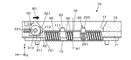
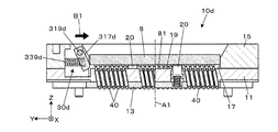
- FIG. 1 is an external view showing a configuration example of the inspection socket 1 of the present embodiment.
- the inspection socket 1 includes a socket body 10, a lid 50, and a pressurizing mechanism 70 as a pressing member.
- the socket body 10 can be taken in and out of the IC package 8 to be inspected, and is attached to the inspection device 9.
- the lid 50 supports the pressurizing mechanism 70 above the socket body 10.
- the pressurizing mechanism 70 is for pressing the inspection target IC package 8 in the lower socket body 10 from above, and applies a load to the inspection target IC package 8.
- the lid 50 is provided with a pair of hooks 60.
- hooks 60 are provided on both the left and right sides.
- the hook 60 is swingably supported by a hook swing shaft 61 along the X-axis direction.
- the hook 60 is a hook swing shaft 61 due to a spring 63.
- the hook 60 on the right side of FIG. 1 is viewed clockwise from the negative X-axis direction, and the hook 60 on the left side of FIG. 1 is viewed from the negative direction of the X-axis. It is urged counterclockwise.
- the hook 60 maintains a state in which the lid 50 covers the upper part of the socket body 10 by engaging the engaging claw 65 with the socket body 10.
- the hook 60 is removed, and the lid 50 is removed from the socket body 10, the inside of the socket body 10 is exposed and the IC package 8 to be inspected can be taken in and out.
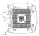
- FIG. 2 is a top view showing a configuration example of the socket body 10.
- FIG. 3 is a cross-sectional view showing a section III-III of FIG.
- FIG. 2 shows the structure of the internal pressing portion 30 by cutting out a part of the guide member 15 (the portion on the left side when facing FIG. 2).
- the socket body 10 includes a pin block 11, a pin plate 13 mounted on the lower surface of the pin block 11, a frame-shaped guide member 15, a pressing portion 30, and an intervening portion.
- the taper member 35 of the above is provided.
- the guide member 15 is placed on the outer peripheral portion of the pin block 11 on the upper surface of the pin block 11.
- the taper member 35 is arranged inside the side portion (left portion in FIG. 2 and the like) of the guide member 15 on the inclined direction side (Y-axis positive direction), which will be described later.
- the pin block 11, the guide member 15, and the taper member 35 form an accommodating recess 17 for accommodating the IC package 8 to be inspected (not shown in FIGS. 2 and 3).
- the IC package 8 to be inspected placed in the storage recess 17 is pushed down from above by the pressurizing mechanism 70, and is housed in a predetermined position of the storage recess 17.
- the pressing portion 30 is for pushing the inspection target IC package 8 accommodated in the accommodating recess 17 in the pressing direction B1.
- the pressing direction B1 is a direction parallel to the negative direction of the Y axis.
- the taper member 35 is interposed between the pressing member 31 and the inspection target IC package 8 when the inspection target IC package 8 is accommodated in the accommodation recess 17.
- the bottom surface of the accommodating recess 17 is a central portion of the upper surface of the pin block 11 and is a portion surrounded by the guide member 15.
- the side wall of the accommodating recess 17 is formed by a guide member 15 and a tapered member 35. Of the side walls of the accommodating recess 17, the three side walls formed by the guide member 15 are fixed, and one side wall formed by the taper member 35 is movable along the Y-axis direction.
- the pin block 11 supports the contact probe 40 on the bottom surface of the accommodating recess 17.
- the contact probe 40 is for conducting the electrode terminal 81 of the IC package 8 to be inspected shown in FIG. 4 or the like with the inspection device 9.
- the electrode terminal 81 is gold, but may be solder.
- the contact probe 40 includes a conductive tube, terminal-side plungers and substrate-side plungers provided at both ends thereof, and a spring provided in the tube. The spring in the tube urges the terminal-side plunger and the substrate-side plunger in a direction away from each other, and the terminal-side plunger and the substrate-side plunger project from both ends of the tube.
- the pin block 11 supports a plurality of contact probes 40 by arranging them along the XY plane so as to correspond to the arrangement of the electrode terminals 81 in the IC package 8 to be inspected. Then, the pin block 11 exposes the upper tip (terminal side plunger) of the contact probe 40 from the exposed surface 19 with the upper surface corresponding to the bottom surface of the accommodating recess 17 as the exposed surface 19.
- the pin block 11 is made of metal.
- the pin block 11 may be made of an insulating resin.
- the pin block 11 has a Z in the central portion thereof in the vertical direction of the exposed surface 19 (the direction parallel to the central axis A1 of the socket body 10 shown by the alternate long and short dash line in FIG. 3). It has a plurality of block-side through holes 111 inclined in a predetermined direction with respect to (axial direction).
- the block-side through hole 111 is a stepped hole having a narrow opening on the upper side (exposed surface 19 side) in order to prevent the contact probe 40 from coming off. Then, by inserting the contact probe 40 into each of the block-side through holes 111, each contact probe 40 is supported in a posture inclined in the above-mentioned predetermined direction (hereinafter, also referred to as “inclination direction”).
- each contact probe 40 The inclination direction of each contact probe 40 is the same.
- a resin material interposed between the pin block 11 and the contact probe 40 is arranged in the vicinity of the opening portion on the upper side (exposed surface 19 side) of the block side through hole 111. With this resin material, the pin block 11 and the contact probe 40 can be brought into a non-contact state.
- the pin block 11 has a plurality of package support portions 20.
- the four package support portions 20 are arranged in the central portion of the pin block 11 so as to avoid the arrangement of the contact probes 40.
- the arrangement position of the package support portion 20 is not limited to the central portion.
- the package support portion 20 includes a spring 201 installed inside the pin block 11 and a spring cap 203 that is placed on the upper portion of the spring 201 and urged upward by the spring 201.
- the pin block 11 is set at a height at which its head (upper end portion of the spring cap 203) protrudes from the exposed surface 19.
- the height of the upper end portion of the spring cap 203 is defined as a height exceeding the tip of the contact probe 40 exposed on the exposed surface 19.
- the pin plate 13 has a plurality of plate-side through holes 131 inclined in the inclination direction at the same inclination angle as the block-side through holes 111 of the pin block 11.
- the plate-side through hole 131 is a stepped hole having a narrow opening on the lower side in order to prevent the contact probe 40 from coming off.
- Each plate-side through-hole 131 corresponds to each of the block-side through-holes 111, and is formed at a position communicating with the corresponding block-side through-hole 111.
- the pin plate 13 penetrates the contact probe 40 inserted into each block-side through-hole 111 through these plate-side through-holes 131, and holds the lower tip (board-side plunger) exposed to the inspection device 9 side. do.
- the pin plate 13 is made of an insulating resin.
- a part of the upper surface of the guide member 15 is a tapered surface inclined toward the accommodating recess 17. Since the guide member 15 has a tapered surface, the IC package 8 to be inspected can be easily taken in and out of the socket body 10.
- the inclination angle of the tapered surface of the guide member 15 can be appropriately set, but it is preferable to set the inclination angle to be the same as that of the tapered surface 351 of the taper member 35.
- the accommodating recess 17 is surrounded by an inclined surface having the same inclination angle, and the IC package 8 to be inspected can be more easily taken in and out of the socket body 10.
- the pressing portion 30 is for pushing the inspection target IC package 8 accommodated in the accommodating recess 17.
- the pressing portion 30 pushes the IC package 8 to be inspected from the side of the accommodating recess 17 in a predetermined pressing direction including a directional component that opposes the inclination direction of the contact probe 40.
- the contact probe 40 is tilted in the positive direction of the Y axis (counterclockwise when viewed from the negative direction of the X axis) with respect to the central axis A1 of the socket body 10. That is, the contact probe 40 is inclined so as to go in the negative direction of the Y axis as it goes in the negative direction of the Z axis. There are a plurality of contact probes 40, all of which are inclined in the same direction.
- the negative direction of the Y-axis, which is opposite to the inclination direction, is defined as the pressing direction B1. Therefore, the pressing portion 30 is installed as a mechanism for pushing the inspection target IC package 8 accommodated in the accommodating recess 17 in the negative direction of the Y axis, which is the pressing direction B1.
- the pressing portion 30 has a pressing member 31 and an elastic member 33 that urges the pressing member 31 in the pressing direction B1.
- the elastic member 33 is elastically deformed by the movement of the pressing member 31 when the IC package 8 to be inspected is accommodated in the accommodating recess 17, and the pressing portion 30 pushes the IC package 8 to be inspected in the pressing direction B1 by the elastic force of the elastic deformation. push.
- the pressing portion 30 pushes the IC package 8 to be inspected in the pressing direction B1 via the taper member 35.
- the pressing member 31 has a roller portion 311 and a support shaft 313 that rotatably supports the roller portion 311.
- the elastic member 33 has a pair of springs 331 and 333 provided at both ends of the support shaft 313 with the inner wall portion of the installation space. Then, the peripheral surface of the roller portion 311 comes into contact with the taper member 35.
- the taper member 35 is a plate body arranged inside the guide member 15 along the side portion on the inclined direction side.
- the tapered member 35 has a tapered surface 351 whose entire upper surface is lowered toward the central portion of the accommodating recess 17. It is sufficient that the accommodation recess 17 has an inclined tapered surface, and a part of the upper surface may be a tapered surface.
- the length of the taper member 35 in the longitudinal direction may exceed the length of the corresponding accommodating recess 17 along the X-axis direction.
- a groove 113 matching the dimensions of the tapered member 35 is formed on the upper surface of the pin block 11.
- the length of the groove portion 113 in the Y-axis direction is wider than the length of the taper member 35 in the Y-axis direction by the movable range C1 pushed and moved by the roller portion 311. Then, the taper member 35 is fitted into the groove portion 113 and is arranged so as to be movable in the Y-axis direction.
- the taper member 35 is provided with a pull-out prevention mechanism (not shown) in order to prevent the taper member 35 from coming off the groove 113 when the IC package 8 to be inspected is attached or detached.
- the taper member 35 is allowed to move along the Y-axis direction between the position in contact with the step in the standard state and the position retracted by the movable range C1 from the position. Therefore, when the IC package 8 to be inspected is put into the socket body 10 and pushed down from above, the taper member 35 moves in the positive direction of the Y axis (the direction opposite to the pressing direction B1), and the IC package 8 to be inspected is accommodated in the recess 17 Is housed in. Then, the IC package 8 to be inspected is in a state of being pushed in the pressing direction B1 from the side in the inclination direction side.
- FIG. 4 and 5 are diagrams for explaining the position change of the pressing portion 30 and the taper member 35 when the IC package 8 to be inspected is accommodated in the accommodating recess 17.
- FIG. 4 shows a cross section III-III of FIG. 2 when the IC package 8 to be inspected is inserted in the socket body 10.
- FIG. 5 shows a cross section III-III of FIG. 2 when the IC package 8 to be inspected is pushed down from above and accommodated in the accommodating recess 17.
- the inspection target IC package 8 is placed on the socket body 10, the inspection target IC package 8 is guided above the accommodating recess 17 by the tapered surface of the guide member 15 and the tapered surface 351 of the taper member 35. Then, it is in a state of being elastically supported by the package support portion 20. Further, in this state, the taper member 35 is pushed by the roller portion 311 by the urging force of the springs 331 and 333 in the pressing direction B1 and is pressed against the step of the groove portion 113.
- the IC package 8 to be inspected receives the elastic force of the springs 331 and 333 in the negative direction of the Y axis via the taper member 35, and is pushed by the pressing portion 30 in the pressing direction B1.
- the end surface (side surface on the negative direction side of the Y axis; the right surface in FIGS. 4 and 5) opposite to the side pressed by the pressing portion 30 of the IC package 8 to be inspected is in contact with the guide member 15. Therefore, the position of the inspection target IC package 8 in the left-right direction (XY plane) is determined, and thereafter, the inspection target IC package 8 only changes its position in the negative direction of the Z axis.
- each contact probe 40 When the IC package 8 to be inspected is further pushed down, the tip (terminal side plunger) of each contact probe 40 exposed from the exposed surface 19 starts to come into contact with the corresponding electrode terminal 81.
- the contact probe 40 can be expanded and contracted in the axial direction (longitudinal direction). Therefore, when the IC package 8 to be inspected is pushed down and the electrode terminal 81 is pressed against the contact probe 40, the contact probe 40 that comes into contact begins to contract.
- the contact probe 40 is arranged so as to be inclined with respect to the direction perpendicular to the exposed surface 19 (Z-axis direction). Further, the position of the IC package 8 to be inspected in the left-right direction (XY plane) is in a fixed state.
- the contact position where the tip of the contact probe 40 is in contact with the electrode terminal 81 of the IC package 8 to be inspected gradually changes according to the descent of the IC package 8 to be inspected (position change in the negative direction of the Z axis).
- the scrubbing operation is performed by scratching the terminal surface.
- a plurality of contact probes 40 can be tilted and supported in a predetermined tilting direction.
- the pressing portion 30 pushes the IC package 8 to be inspected housed in the accommodating recess 17 in the pressing direction B1 including a direction component that opposes the tilting direction of the contact probe 40.
- the tilting direction is a direction tilted in the Y-axis positive direction with respect to the direction perpendicular to the exposed surface 19 (Z-axis direction)
- the pressing direction B1 is the Y-axis which is a directional component against the tilting direction. It was in the negative direction.
- the contact position where the tip of the contact probe 40 is in contact with the electrode terminal 81 of the IC package 8 to be inspected moves in the pressing direction of the IC package 8 to be inspected (position change in the negative Z-axis direction). It changes gradually accordingly.
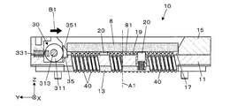
- FIG. 6 is a diagram showing a configuration example of the socket body 10b in the first modification.
- FIG. 7 is a cross-sectional view showing a cross section of VII-VII of FIG. 6, showing a state in which the IC package 8 to be inspected is pushed down from above and accommodated in the accommodating recess 17.
- FIGS. 6 and 7 the same configurations as those in the above embodiment are designated by the same reference numerals.
- the socket body 10b of the modified example 1 includes a pin block 11, a pin plate 13, a guide member 15, and a pressing portion 30.
- the configuration of the pressing portion 30 is the same as that of the above embodiment, and the roller portion 311 is urged by the springs 331 and 333 in the pressing direction B1 via the support shaft 313.
- the socket body 10b does not include the taper member 35 of the above embodiment.
- the IC package 8 to be inspected When the IC package 8 to be inspected is placed on the socket body 10b and a load is applied to the IC package 8 to be inspected by the pressurizing mechanism 70, the IC package 8 to be inspected is pushed down, the spring 201 contracts, and the package support portion. The support position by 20 is lowered. Then, the roller portion 311 abuts on the side end of the IC package 8 to be inspected and is pushed so as to retract in the positive direction of the Y axis, and the springs 331 and 333 contract. The IC package 8 to be inspected receives the elastic force of the springs 331 and 333 in the negative direction of the Y axis via the roller portion 311 and is pushed by the pressing portion 30 in the pressing direction B1.
- the end surface (side surface on the negative direction side of the Y axis; the right surface in FIGS. 6 and 7) opposite to the side pressed by the pressing portion 30 of the IC package 8 to be inspected is in contact with the guide member 15. Therefore, the position of the inspection target IC package 8 in the left-right direction (XY plane) is determined, and thereafter, the inspection target IC package 8 only changes its position in the negative direction of the Z axis.
- each contact probe 40 When the IC package 8 to be inspected is further pushed down, the tip (terminal side plunger) of each contact probe 40 exposed from the exposed surface 19 starts to come into contact with the corresponding electrode terminal 81.
- the contact probe 40 can be expanded and contracted in the axial direction (longitudinal direction). Therefore, when the IC package 8 to be inspected is pushed down and the electrode terminal 81 is pressed against the contact probe 40, the contact probe 40 that comes into contact begins to contract.
- the contact probe 40 is arranged so as to be inclined with respect to the direction perpendicular to the exposed surface 19 (Z-axis direction). Further, the position of the IC package 8 to be inspected in the left-right direction (XY plane) is in a fixed state.
- the contact position where the tip of the contact probe 40 is in contact with the electrode terminal 81 of the IC package 8 to be inspected gradually changes according to the descent of the IC package 8 to be inspected (position change in the negative direction of the Z axis).
- the scrubbing operation is performed by scratching the terminal surface.
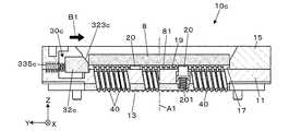
- FIG. 8 is a diagram showing a configuration example of the socket body 10c in the modified example 2.
- FIG. 9 is a cross-sectional view showing the IX-IX cross section of FIG. 8, showing a state in which the IC package 8 to be inspected is pushed down from above and housed in the storage recess 17.
- FIGS. 8 and 9 the same configurations as those in the above embodiment are designated by the same reference numerals.
- the socket body 10c of the modified example 2 includes a pin block 11, a pin plate 13, a guide member 15, and a pressing portion 30c.
- the pressing portion 30c has a tapered member 32c as a pressing member instead of the roller portion 311 of the first modification.
- the pressing portion 30c has a pair of springs 335c and 337c provided between the tapered member 32c and the inner wall portion of the installation space thereof as an elastic member for urging the tapered member 32c in the pressing direction B1.
- the taper member 32c has a long plate-shaped portion 321c as a whole along the X-axis direction.
- the central portion of the plate-shaped portion 321c in the longitudinal direction has a wide shape.
- the plate-shaped portion 321c forms a part of the side wall of the accommodating recess 17.
- the tapered member 32c has a tapered surface 323c in which a part of the upper surface of the plate-shaped portion 321c is lowered toward the central portion of the accommodating recess 17. It should be noted that the entire upper surface may be a tapered surface.
- the IC package 8 to be inspected When the IC package 8 to be inspected is placed in the socket body 10c and a load is applied to the IC package 8 to be inspected by the pressurizing mechanism 70, the IC package 8 to be inspected is pushed down, the spring 201 contracts, and the package support portion. The support position by 20 is lowered. Then, the plate-shaped portion 321c of the taper member 32c abuts on the side end of the IC package 8 to be inspected and is pushed so as to retract in the positive direction of the Y axis, and the springs 335c and 337c are contracted by the retracting taper member 32c.
- the IC package 8 to be inspected receives the elastic force of the springs 335c and 337c in the negative direction of the Y axis, and is pushed by the pressing portion 30c in the pressing direction B1.
- the end surface (side surface on the negative direction side of the Y axis; right side surface in FIGS. 8 and 9) opposite to the side pressed by the pressing portion 30c of the IC package 8 to be inspected is in contact with the guide member 15. Therefore, the position of the inspection target IC package 8 in the left-right direction (XY plane) is determined, and thereafter, the inspection target IC package 8 only changes its position in the negative direction of the Z axis.
- each contact probe 40 When the IC package 8 to be inspected is further pushed down, the tip (terminal side plunger) of each contact probe 40 exposed from the exposed surface 19 starts to come into contact with the corresponding electrode terminal 81.
- the contact probe 40 can be expanded and contracted in the axial direction (longitudinal direction). Therefore, when the IC package 8 to be inspected is pushed down and the electrode terminal 81 is pressed against the contact probe 40, the contact probe 40 that comes into contact begins to contract.
- the contact probe 40 is arranged so as to be inclined with respect to the direction perpendicular to the exposed surface 19 (Z-axis direction). Further, the position of the IC package 8 to be inspected in the left-right direction (XY plane) is in a fixed state.
- the contact position where the tip of the contact probe 40 is in contact with the electrode terminal 81 of the IC package 8 to be inspected gradually changes according to the descent of the IC package 8 to be inspected (position change in the negative direction of the Z axis).
- the scrubbing operation is performed by scratching the terminal surface.
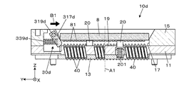
- FIGS. 10 and 11 are vertical cross-sectional views showing a configuration example of the socket body 10d in the modified example 3, and show a change in the pressing portion 30d when the IC package 8 to be inspected is housed in the housing recess 17.
- FIG. 10 shows a state in which the IC package 8 to be inspected is inserted in the socket body 10d.
- FIG. 11 shows a state in which the IC package 8 to be inspected is pushed down from above and housed in the storage recess 17.
- FIGS. 10 and 11 the same reference numerals are given to the same configurations as those in the above embodiment.
- the socket body 10d of the modified example 3 includes a pin block 11, a pin plate 13, a guide member 15, and a pressing portion 30d.
- the pressing portion 30d has a rocking body 317d that is swingably supported by a rocking shaft 319d along the X-axis direction as a pressing member. Further, the pressing portion 30d has a spring 339d as an elastic member that urges the rocking body 317d in the pressing direction B1.
- the spring 339d is arranged in a movable space of the rocking body 317d provided in the side wall of the accommodating recess 17 in a posture of urging the rocking body 317d in the pressing direction B1.
- the rocking body 317d is arranged in a posture inclined at an angle similar to the tapered surface of the guide member 15 in a natural state in which the IC package 8 to be inspected is not placed.
- the IC package 8 to be inspected When the IC package 8 to be inspected is placed on the socket body 10d, the IC package 8 to be inspected is guided above the accommodating recess 17 by the tapered surface of the guide member 15 and the inclined surface of the rocking body 317d, and is elastic by the package support portion 20. It will be in a supported state (state in FIG. 10).
- the IC package 8 to be inspected is pushed down, the spring 201 contracts, and the support position by the package support portion 20 is lowered. Then, the rocking body 317d comes into contact with the side end of the IC package 8 to be inspected, rotates clockwise with respect to the swinging shaft 319d in the negative direction of the X axis, and contracts the spring 339d.
- the IC package 8 to be inspected receives the elastic force of the contracted spring 339d in the negative direction of the Y axis, and is pushed by the pressing portion 30d in the pressing direction B1.
- the end surface (side surface on the negative direction side of the Y axis; right side surface in FIGS. 10 and 11) opposite to the side pressed by the pressing portion 30d of the IC package 8 to be inspected is in contact with the guide member 15. Therefore, the position of the inspection target IC package 8 in the left-right direction (XY plane) is determined, and thereafter, the inspection target IC package 8 only changes its position in the negative direction of the Z axis.
- each contact probe 40 When the IC package 8 to be inspected is further pushed down, the tip (terminal side plunger) of each contact probe 40 exposed from the exposed surface 19 starts to come into contact with the corresponding electrode terminal 81.
- the contact probe 40 can be expanded and contracted in the axial direction (longitudinal direction). Therefore, when the IC package 8 to be inspected is pushed down and the electrode terminal 81 is pressed against the contact probe 40, the contact probe 40 that comes into contact begins to contract.
- the contact probe 40 is arranged so as to be inclined with respect to the direction perpendicular to the exposed surface 19 (Z-axis direction). Further, the position of the IC package 8 to be inspected in the left-right direction (XY plane) is in a fixed state.
- the contact position where the tip of the contact probe 40 is in contact with the electrode terminal 81 of the IC package 8 to be inspected gradually changes according to the descent of the IC package 8 to be inspected (position change in the negative direction of the Z axis).
- the scrubbing operation is performed by scratching the terminal surface.
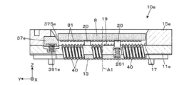
- FIG. 12 is a diagram showing a configuration example of the socket body 10e in the modified example 4.
- 13 and 14 are cross-sectional views showing a cross section of XIII-XIII of FIG.
- FIG. 13 shows a state in which the IC package 8 to be inspected is inserted in the socket body 10e.
- FIG. 14 shows a state in which the IC package 8 to be inspected is pushed down from above and housed in the storage recess 17.
- the same configurations as those in the above embodiment are designated by the same reference numerals.
- the socket body 10e of the modified example 4 is an elastic member that urges the pin block 11e, the pin plate 13, the guide member 15e, the taper member 37e, and the taper member 37e upward.
- a pair of springs 391e and 393e are provided.
- the taper member 37e has a long plate-shaped portion 371e as a whole along the X-axis direction.
- the central portion of the plate-shaped portion 371e in the longitudinal direction has a wide shape.
- the plate-shaped portion 371e forms a part of the side wall of the accommodating recess 17.
- the taper member 37e is supported so as to be displaceable in the vertical direction by two springs 391e and 393e that urge the taper member 37e upward.
- the taper member 37e has a tapered surface 375e in which a part of the upper surface of the plate-shaped portion 371e is lowered toward the bottom surface of the accommodating recess 17.
- One end of the springs 391e and 393e is installed inside the wide portion 373e, and the other end is installed inside the pin block 11e below it.
- the IC package 8 to be inspected When the IC package 8 to be inspected is placed on the socket body 10e, the IC package 8 to be inspected is guided above the accommodating recess 17 by the tapered surface of the guide member 15e and the tapered surface 375e of the tapered member 37e, and is guided by the package support portion 20. It is in an elastically supported state (the state shown in FIG. 13).
- the IC package 8 to be inspected is pushed down, the spring 201 contracts, and the support position by the package support portion 20 is lowered. Then, the IC package 8 to be inspected moves along the tapered surface 375e of the tapered member 37e. Therefore, the IC package 8 to be inspected tends to move in the negative Z-axis direction and the negative Y-axis along the inclined surface of the tapered surface 375e.
- the end surface side surface on the negative direction side of the Y axis; the right surface in FIGS.
- the position of the inspection target IC package 8 in the left-right direction (XY plane) is determined, and thereafter, the inspection target IC package 8 only changes its position in the negative direction of the Z axis.
- each contact probe 40 When the IC package 8 to be inspected is further pushed down, the tip (terminal side plunger) of each contact probe 40 exposed from the exposed surface 19 starts to come into contact with the corresponding electrode terminal 81.
- the contact probe 40 can be expanded and contracted in the axial direction (longitudinal direction). Therefore, when the IC package 8 to be inspected is pushed down and the electrode terminal 81 is pressed against the contact probe 40, the contact probe 40 that comes into contact begins to contract.
- the contact probe 40 is arranged so as to be inclined with respect to the direction perpendicular to the exposed surface 19 (Z-axis direction). Further, the position of the IC package 8 to be inspected in the left-right direction (XY plane) is in a fixed state.
- the contact position where the tip of the contact probe 40 is in contact with the electrode terminal 81 of the IC package 8 to be inspected gradually changes according to the descent of the IC package 8 to be inspected (position change in the negative direction of the Z axis).
- the scrubbing operation is performed by scratching the terminal surface.
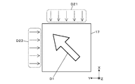
- Modification 5 In the above-described embodiment and each modification, a configuration in which the IC package to be inspected is pushed in one direction is illustrated. On the other hand, depending on the tilting direction of the contact probe, the IC package to be inspected may be pushed in a plurality of directions.
- FIG. 15 is a schematic view showing the relationship between the tilting direction of the contact probe supported at the bottom of the accommodating recess 17 and the pushing direction of the IC package to be inspected.
- FIG. 15 is a top view of the accommodating recess 17 as in FIGS. 2, 6, 8 and 12.
- the X-axis direction, Y-axis direction, and Z-axis direction are the same as the directions shown in other drawings.
- the inclination direction of the contact probe was the left direction (Y-axis positive direction) with respect to the drawing, but in the present modification 5, as shown by the arrow D1, the contact probe is oriented toward FIG. It is diagonally upward to the left (X-axis positive direction and Y-axis positive direction).
- the IC package to be inspected is pushed in the direction D21 (X-axis negative direction) and the direction D23 (Y-axis negative direction), which are the directions including the direction component opposite to the inclination direction D1.
- any of the pressing portions 30, 30c, and 30d shown in the above-described embodiment and the modified examples 1 to 3 is installed on the X-axis positive direction side and the Y-axis positive direction side.
- the types of pressing portions installed on the positive direction side of the X axis and the positive direction side of the Y axis may be different.
- the IC package 8 to be inspected is pushed in the direction D21 (negative X-axis direction) and in the direction D23 (negative Y-axis).
- the taper members 37e and the springs 391e and 393e of the modified example 4 may be installed on the X-axis positive direction side and the Y-axis positive direction side, and the IC package to be inspected may be pushed in the directions D21 and D23.
- An aspect of the present disclosure is an inspection in which a pin block that exposes the tip of a contact probe from an exposed surface and supports the contact probe by inclining it in a predetermined direction with respect to a direction perpendicular to the exposed surface, and contacting the contact probe.
- An inspection socket including a pressing portion for pushing the target IC package.
- the pin block can support the contact probe by inclining it in a predetermined direction.
- the IC package to be inspected can be pushed by the pressing portion. Since the pin block is tilted in a predetermined direction, when the contact probe comes into contact with the electrode terminal of the IC package to be inspected, the IC package to be inspected moves based on the tilt direction of the contact probe, and scrubbing operation is unlikely to occur. May occur. However, since the IC package to be inspected is pushed by the pressing portion, such a situation can be suppressed, and a stable scrub operation can be performed when the contact probe and the electrode terminal of the IC package to be inspected come into contact with each other.
- each contact probe since the inclination direction of each contact probe may be the same, it is not necessary to increase the size of the pin block, and complicated processing is not required for the pin block that supports the contact probe. Further, since the IC package to be inspected is pushed by the pressing portion, the positioning accuracy of the IC package to be inspected can be improved as compared with the case where there is no pressing portion.
- the pressing portion may push the IC package to be inspected in a pressing direction including a directional component that opposes the predetermined direction.
- the pressing direction may be a direction parallel to the plate surface of the IC package to be inspected.
- the IC package to be inspected is pressurized in the direction perpendicular to the plate surface of the IC package to be inspected. Since the pressing direction is parallel to the plate surface of the IC package to be inspected, the pressing direction and the pressing direction can be different directions. Therefore, the IC package itself to be inspected is less likely to be damaged as compared with the case where the pressing direction and the pressing direction are parallel to each other.
- the pressing portion may have a pressing member and an elastic member that urges the pressing member.
- the pressing member may have a roller portion.
- the roller unit can push the IC package to be inspected, and the IC package to be inspected can be prevented from being damaged.
- the urging direction of the elastic member and the pressing direction may be parallel.
- An intervening portion may be provided, and the pressing portion may push the IC package to be inspected through the intervening portion.
- the pressing portion Since the IC package to be inspected can be pushed through the intervening portion, the pressing portion does not directly push the IC package to be inspected, and damage to the IC package to be inspected can be prevented.
- the intervening portion may have a tapered surface.
- the contact probe and the electrode terminal of the IC package to be inspected are brought into contact with each other, the IC package to be inspected can be moved along the tapered surface, so that the IC package to be inspected can be easily replaced.
Landscapes
- Physics & Mathematics (AREA)
- General Physics & Mathematics (AREA)
- Engineering & Computer Science (AREA)
- Computer Hardware Design (AREA)
- Microelectronics & Electronic Packaging (AREA)
- Testing Of Individual Semiconductor Devices (AREA)
- Measuring Leads Or Probes (AREA)
- Connecting Device With Holders (AREA)
Priority Applications (2)
| Application Number | Priority Date | Filing Date | Title |
|---|---|---|---|
| US17/792,146 US20230050000A1 (en) | 2020-01-30 | 2020-12-16 | Inspection socket |
| CN202080094969.3A CN115023865A (zh) | 2020-01-30 | 2020-12-16 | 检查用插座 |
Applications Claiming Priority (2)
| Application Number | Priority Date | Filing Date | Title |
|---|---|---|---|
| JP2020-013689 | 2020-01-30 | ||
| JP2020013689A JP2021120924A (ja) | 2020-01-30 | 2020-01-30 | 検査用ソケット |
Publications (1)
| Publication Number | Publication Date |
|---|---|
| WO2021153061A1 true WO2021153061A1 (ja) | 2021-08-05 |
Family
ID=77078884
Family Applications (1)
| Application Number | Title | Priority Date | Filing Date |
|---|---|---|---|
| PCT/JP2020/046951 Ceased WO2021153061A1 (ja) | 2020-01-30 | 2020-12-16 | 検査用ソケット |
Country Status (5)
| Country | Link |
|---|---|
| US (1) | US20230050000A1 (https=) |
| JP (1) | JP2021120924A (https=) |
| CN (1) | CN115023865A (https=) |
| TW (1) | TW202129292A (https=) |
| WO (1) | WO2021153061A1 (https=) |
Families Citing this family (1)
| Publication number | Priority date | Publication date | Assignee | Title |
|---|---|---|---|---|
| KR102788961B1 (ko) * | 2022-08-02 | 2025-04-01 | 주식회사 오킨스전자 | 반도체 패키지 테스트 장치 |
Citations (4)
| Publication number | Priority date | Publication date | Assignee | Title |
|---|---|---|---|---|
| US20050095906A1 (en) * | 2003-10-31 | 2005-05-05 | Hon Hai Precision Ind. Co., Ltd. | Socket connector with reliable retaining means |
| JP2008034173A (ja) * | 2006-07-27 | 2008-02-14 | Yokowo Co Ltd | 検査用ソケット |
| US20100159732A1 (en) * | 2008-12-22 | 2010-06-24 | Hon Hai Precision Industry Co., Ltd. | Socket connector having metallic positioning member securing electronic device therein |
| US20180172730A1 (en) * | 2006-12-21 | 2018-06-21 | Essai, Inc. | Contactor with angled depressible probes |
Family Cites Families (9)
| Publication number | Priority date | Publication date | Assignee | Title |
|---|---|---|---|---|
| US5476211A (en) * | 1993-11-16 | 1995-12-19 | Form Factor, Inc. | Method of manufacturing electrical contacts, using a sacrificial member |
| JP2000195626A (ja) * | 1998-12-25 | 2000-07-14 | Yokowo Co Ltd | Icソケットおよびicソケットへのicパッケ―ジの装着機構 |
| US7247035B2 (en) * | 2000-06-20 | 2007-07-24 | Nanonexus, Inc. | Enhanced stress metal spring contactor |
| US6917525B2 (en) * | 2001-11-27 | 2005-07-12 | Nanonexus, Inc. | Construction structures and manufacturing processes for probe card assemblies and packages having wafer level springs |
| JP2002043004A (ja) * | 2000-07-19 | 2002-02-08 | Nec Yamagata Ltd | Icソケット |
| JP2006200975A (ja) * | 2005-01-19 | 2006-08-03 | Matsushita Electric Ind Co Ltd | 半導体装置の検査方法および検査装置および接触端子 |
| US7479794B2 (en) * | 2007-02-28 | 2009-01-20 | Sv Probe Pte Ltd | Spring loaded probe pin assembly |
| JP5636908B2 (ja) * | 2010-11-24 | 2014-12-10 | 富士通株式会社 | ソケットおよび電子装置 |
| JP5991823B2 (ja) * | 2012-02-14 | 2016-09-14 | 株式会社日本マイクロニクス | 電気的接続装置及びその組立方法 |
-
2020
- 2020-01-30 JP JP2020013689A patent/JP2021120924A/ja active Pending
- 2020-12-16 US US17/792,146 patent/US20230050000A1/en not_active Abandoned
- 2020-12-16 CN CN202080094969.3A patent/CN115023865A/zh active Pending
- 2020-12-16 WO PCT/JP2020/046951 patent/WO2021153061A1/ja not_active Ceased
- 2020-12-22 TW TW109145500A patent/TW202129292A/zh unknown
Patent Citations (4)
| Publication number | Priority date | Publication date | Assignee | Title |
|---|---|---|---|---|
| US20050095906A1 (en) * | 2003-10-31 | 2005-05-05 | Hon Hai Precision Ind. Co., Ltd. | Socket connector with reliable retaining means |
| JP2008034173A (ja) * | 2006-07-27 | 2008-02-14 | Yokowo Co Ltd | 検査用ソケット |
| US20180172730A1 (en) * | 2006-12-21 | 2018-06-21 | Essai, Inc. | Contactor with angled depressible probes |
| US20100159732A1 (en) * | 2008-12-22 | 2010-06-24 | Hon Hai Precision Industry Co., Ltd. | Socket connector having metallic positioning member securing electronic device therein |
Also Published As
| Publication number | Publication date |
|---|---|
| US20230050000A1 (en) | 2023-02-16 |
| JP2021120924A (ja) | 2021-08-19 |
| CN115023865A (zh) | 2022-09-06 |
| TW202129292A (zh) | 2021-08-01 |
Similar Documents
| Publication | Publication Date | Title |
|---|---|---|
| KR102001351B1 (ko) | 인터페이스 장치, 인터페이스 유닛, 프로브 장치 및 접속 방법 | |
| CN103311709B (zh) | 用于电子装置的触头 | |
| KR101245837B1 (ko) | 반도체 패키지 테스트용 소켓장치 | |
| CN109406835B (zh) | 电连接装置 | |
| JP2019009030A (ja) | ソケット | |
| JP2003167001A (ja) | 電子部品用ソケットのコンタクトプローブ及びこれを用いた電子部品用ソケット | |
| KR102806902B1 (ko) | 프로브 핀 | |
| JPWO2017179320A1 (ja) | プローブピン及びこれを用いた電子デバイス | |
| CN105103386A (zh) | 电接触件和电子部件用插槽 | |
| KR102046808B1 (ko) | 양방향 도전성 핀, 이를 이용한 양방향 도전성 모듈 및 그 제조방법 | |
| JP5673366B2 (ja) | 半導体素子用ソケット | |
| WO2021153061A1 (ja) | 検査用ソケット | |
| KR101778608B1 (ko) | 전기 신호 연결용 마이크로 컨택터 | |
| CN112470011B (zh) | 接触针及电子部件用插座 | |
| KR102683627B1 (ko) | 롱 스트로크를 가진 포고핀 | |
| KR101041219B1 (ko) | 검사용 컨택모듈 | |
| KR20230076513A (ko) | 프로브 카드 | |
| KR102738445B1 (ko) | 카메라 모듈의 측면 저항 측정을 위한 사이드 컨텍 소켓 | |
| JP2020149857A (ja) | ソケット | |
| JP2020134215A (ja) | プローブユニット | |
| JP2010281675A (ja) | 電子部品検査装置及び電子部品検査方法 | |
| KR200177290Y1 (ko) | 반도체 패키지용 테스트장치 | |
| TWI689735B (zh) | 測試載具及其應用之測試設備 | |
| JP2025024953A (ja) | ソケット及び検査用ソケット | |
| JP6898827B2 (ja) | ソケット |
Legal Events
| Date | Code | Title | Description |
|---|---|---|---|
| 121 | Ep: the epo has been informed by wipo that ep was designated in this application |
Ref document number: 20916562 Country of ref document: EP Kind code of ref document: A1 |
|
| NENP | Non-entry into the national phase |
Ref country code: DE |
|
| 122 | Ep: pct application non-entry in european phase |
Ref document number: 20916562 Country of ref document: EP Kind code of ref document: A1 |